tpsm53604 36-v input, 4-a power module in rlf qfn package ... · line regulation ta = +25°c, iout...
TRANSCRIPT

VIN
PGND
VIN
VOUT VOUT
FB
PGOOD
EN
V5V
TPSM53604
AGND
CIN
RFBT
RFBB
COUT
Output Current (A)
Effic
iency (
%)
0 1 2 3 430
35
40
45
50
55
60
65
70
75
80
85
90
95
100
VOUT = 5 V
EFF5
VIN
12 V24 V
Product
Folder
Order
Now
Technical
Documents
Tools &
Software
Support &Community
An IMPORTANT NOTICE at the end of this data sheet addresses availability, warranty, changes, use in safety-critical applications,intellectual property matters and other important disclaimers. PRODUCTION DATA.
TPSM53604SNVSBC9A –NOVEMBER 2019–REVISED DECEMBER 2019
TPSM53604 36-V Input, 4-A Power Module in RLF QFN Package
1
1 Features1• 5 mm × 5.5 mm × 4 mm routable lead-frame
(RLF) QFN package– Industry’s smallest 36-V, 4-A footprint:
85 mm2 solution size (single sided)– Low EMI: Meets CISPR11 radiated emissions– Excellent thermal performance:
Up to 20 W output power at 85ºC, no airflow– Standard footprint: single large thermal pad
and all pins accessible from perimeter• 3.8 V to 36 V input voltage range• Output voltage range: 1 V to 7 V• Efficiency up to 95%• Power-good flag• Precision enable• Built-in hiccup-mode short-circuit protection, over-
temperature protection, start-up into pre-biasoutput, soft start, and UVLO
• Operating IC junction range: –40°C to +125°C• Operating ambient range: –40°C to +105°C• Shock and vibration tested to Mil-STD-883D• Pin compatible with: 3-A TPSM53603
and 2-A TPSM53602• Create a custom design using the TPSM53604
with the WEBENCH® Power Designer
2 Applications• General purpose wide VIN power supplies• Factory automation and control• Test and measurement• Aerospace and defense• Negative output voltage applications
3 DescriptionThe TPSM53604 power module is a highly integrated4-A power solution that combines a 36-V input, step-down, DC/DC converter with power MOSFETs, ashielded inductor, and passives in a thermally-enhanced QFN package. The 5 mm x 5.5 mm x4 mm, 15-pin QFN package uses routable lead-frametechnology for enhanced thermal performance, smallfootprint, and low EMI. The package footprint has allpins accessible from the perimeter and a single largethermal pad for simple layout and easy handling inmanufacturing.
The total solution requires as few as four externalcomponents and eliminates the loop compensationand magnetics part selection from the designprocess. The full feature set includes power good,programmable UVLO, prebias start-up, overcurrent,and overtemperature protections, making theTPSM53604 an excellent device for powering a widerange of applications.
Device Information(1)DEVICE NUMBER PACKAGE BODY SIZE (NOM)
TPSM53604 QFN-RLFMOD (15) 5.0 mm × 5.5 mm
(1) For all available packages, see the orderable addendum atthe end of the data sheet.
RLF Package and Typical Layout
Simplified Schematic 5 VOUT Efficiency

2
TPSM53604SNVSBC9A –NOVEMBER 2019–REVISED DECEMBER 2019 www.ti.com
Product Folder Links: TPSM53604
Submit Documentation Feedback Copyright © 2019, Texas Instruments Incorporated
Table of Contents1 Features .................................................................. 12 Applications ........................................................... 13 Description ............................................................. 14 Revision History..................................................... 25 Pin Configuration and Functions ......................... 36 Specifications......................................................... 4
6.1 Absolute Maximum Ratings ...................................... 46.2 ESD Ratings.............................................................. 46.3 Recommended Operating Conditions....................... 46.4 Thermal Information .................................................. 56.5 Electrical Characteristics........................................... 56.6 Typical Characteristics (VIN = 5 V)............................ 76.7 Typical Characteristics (VIN = 12 V).......................... 86.8 Typical Characteristics (VIN = 24 V).......................... 96.9 Typical Characteristics (VIN = 36 V)........................ 10
7 Detailed Description ............................................ 117.1 Overview ................................................................. 117.2 Functional Block Diagram ....................................... 117.3 Feature Description................................................. 127.4 Device Functional Modes........................................ 19
8 Application and Implementation ........................ 208.1 Application Information............................................ 208.2 Typical Application .................................................. 20
9 Power Supply Recommendations ...................... 2210 Layout................................................................... 23
10.1 Layout Guidelines ................................................. 2310.2 Layout Examples................................................... 2310.3 Theta JA versus PCB Area................................... 2410.4 Package Specifications ......................................... 2510.5 EMI........................................................................ 25
11 Device and Documentation Support ................. 2711.1 Device Support...................................................... 2711.2 Documentation Support ........................................ 2711.3 Receiving Notification of Documentation Updates 2711.4 Support Resources ............................................... 2711.5 Trademarks ........................................................... 2711.6 Electrostatic Discharge Caution............................ 2711.7 Glossary ................................................................ 28
12 Mechanical, Packaging, and OrderableInformation ........................................................... 28
4 Revision HistoryNOTE: Page numbers for previous revisions may differ from page numbers in the current version.
Changes from Original (November 2019) to Revision A Page
• Changed device status from Advance Information to Production Data ................................................................................. 1

2
3
4
5
6
13
12
11
10
9
1 14
15
7 8
VIN
EN
NC
DNC
DNC
PGOOD
VOUT VOUT
FB
NC
NC
AGND
V5V
VIN
PGND
3
TPSM53604www.ti.com SNVSBC9A –NOVEMBER 2019–REVISED DECEMBER 2019
Product Folder Links: TPSM53604
Submit Documentation FeedbackCopyright © 2019, Texas Instruments Incorporated
5 Pin Configuration and Functions
RDA Package15-Pin QFNTop View
Pin FunctionsPIN
TYPE DESCRIPTIONNO. NAME
12 AGND GAnalog ground. Zero voltage reference for internal references and logic. All electrical parameters aremeasured with respect to this pin. This pin must be connected to PGND at a single point. See theLayout section for a recommended layout.
4, 5 DNC — Do not connect. Do not connect these pins to ground, to another DNC pin, or to any other voltage. Thesepins are connected to internal circuitry. Each pin must be soldered to an isolated pad.
2 EN IEnable pin. This pin turns the converter on when pulled high and turns off the converter when pulled low.This pin can be connected directly to VIN. Do not float. This pin can be used to set the input undervoltage lockout with two resistors. See the Programmable Undervoltage Lockout (UVLO) section.
9 FB IFeedback input. Connect the mid-point of the feedback resistor divider to this pin. Connect the upperresistor (RFBT) of the feedback divider to VOUT at the desired point of regulation. Connect the lowerresistor (RFBB) of the feedback divider to AGND.
3, 10,11 NC —
Not connected. These pins are not connected to any circuitry within the module. It is recommended thatthese pins be connected to the PGND plane on the application board to enhance shielding and thermalperformance.
15 PGND GPower ground. This is the return current path for the power stage of the device. Connect this pad to theinput supply return, the load return, and the capacitors associated with the VIN and VOUT pins. See theLayout section for a recommended layout.
6 PGOOD OPower-good pin. Open-drain output that asserts low if the feedback voltage is not within the specifiedwindow thresholds. A 10-kΩ to 100-kΩ pullup resistor is required and can be tied to the V5V pin or otherDC voltage less than 22 V. If not used, this pin can be left open or connected to PGND.
1, 14 VIN I Input supply voltage. Connect the input supply to these pins. Connect input capacitors between thesepins and PGND in close proximity to the device.
7, 8 VOUT O Output voltage. These pins are connected to the internal output inductor. Connect these pins to the outputload and connect external output capacitors between these pins and PGND.
13 V5V O Internal 5-V LDO output. Supplies internal control circuits. Do not connect to external loads. This pin canbe used as logic supply for PGOOD pin.

4
TPSM53604SNVSBC9A –NOVEMBER 2019–REVISED DECEMBER 2019 www.ti.com
Product Folder Links: TPSM53604
Submit Documentation Feedback Copyright © 2019, Texas Instruments Incorporated
(1) Stresses beyond those listed under Absolute Maximum Ratings may cause permanent damage to the device. These are stress ratingsonly, which do not imply functional operation of the device at these or any other conditions beyond those indicated under RecommendedOperating Conditions. Exposure to absolute-maximum-rated conditions for extended periods may affect device reliability.
(2) The voltage on this pin must not exceed the voltage on the VIN pin by more than 0.3 V.(3) The ambient temperature is the air temperature of the surrounding environment. The junction temperature is the temperature of the
internal power IC when the device is powered. Operating below the maximum ambient temperature, as shown in the safe operating area(SOA) curves in the typical characteristics sections, ensures that the maximum junction temperature of any component inside themodule is never exceeded.
6 Specifications
6.1 Absolute Maximum RatingsOver the recommended operating junction temperature range (1)
PARAMETER MIN MAX UNIT
Input voltage
VIN to PGND –0.3 38
V
EN to AGND (2) –0.3 VIN + 0.3
PGOOD to AGND (2) –0.3 22
FB to AGND –0.3 5.5
AGND to PGND –0.3 0.3
Output voltageVOUT to PGND (2) -0.3 VIN + 0.3
VV5V to AGND 0 5.5
Operating IC junction temperature, TJ(3) –40 150 °C
Storage temperature, Tstg –55 150 °C
Peak reflow case temperature 245 °C
Maximum number or reflows allowed 3
Mechanical vibration Mil-STD-883D, Method 2007.2, 20 to 2000 Hz 20 G
Mechanical shock Mil-STD-883D, Method 2002.3, 1 msec, 1/2 sine, mounted 500 G
(1) JEDEC document JEP155 states that 500-V HBM allows safe manufacturing with a standard ESD control process.(2) JEDEC document JEP157 states that 250-V CDM allows safe manufacturing with a standard ESD control process.
6.2 ESD RatingsVALUE UNIT
V(ESD) Electrostatic dischargeHuman-body model (HBM) (1) ±2500
VCharged-device model (CDM) (2) ±1000
(1) Recommended operating conditions indicate conditions for which the device is intended to be functional, but do not ensure specificperformance limits. For ensured specifications, see Electrical Characteristics.
(2) The recommended minimum VIN is 3.8 V or (VOUT + 1 V), whichever is greater. See the Voltage Dropout section for more information.(3) The recommended maximum output voltage varies depending input voltage. See the Voltage Dropout section for more information.(4) The voltage on this pin must not exceed the voltage on the VIN pin by more than 0.3 V.(5) Minimum CIN of 20 µF must be ceramic type.(6) The minimum amount of required output capacitance varies depending on the output voltage (see Table 1).
6.3 Recommended Operating ConditionsOver operating ambient temperature range (unless otherwise noted) (1)
MIN MAX UNIT
Input voltage, VIN 3.8 (2) 36 V
Output voltage, VOUT 1 7 (3) V
Output current, IOUT 0 4 A
EN voltage, VEN(4) 0 VIN V
PGOOD pullup voltage, VPGOOD(4) 0 18 V
PGOOD sink current 3 mA
Operating ambient temperature, TA –40 105 °C
Input capacitance, CIN 20 (5) µF
Output capacitance, COUT min (6) 1000 µF

5
TPSM53604www.ti.com SNVSBC9A –NOVEMBER 2019–REVISED DECEMBER 2019
Product Folder Links: TPSM53604
Submit Documentation FeedbackCopyright © 2019, Texas Instruments Incorporated
(1) For more information about traditional and new thermal metrics, see the Semiconductor and IC Package Thermal Metrics applicationreport.
(2) The junction-to-ambient thermal resistance, RθJA, applies to devices soldered directly to a 75 mm x 75 mm four-layer PCB with 2 oz.copper and natural convection cooling. Additional airflow and PCB copper area reduces RθJA. For more information, see the Theta JAversus PCB Area section.
(3) The junction-to-top board characterization parameter, ψJT, estimates the junction temperature, TJ, of a device in a real system, using aprocedure described in JESD51-2A (section 6 and 7). TJ = ψJT × Pdis + TT; where Pdis is the power dissipated in the device and TT isthe temperature of the top of the device.
(4) The junction-to-board characterization parameter, ψJB, estimates the junction temperature, TJ, of a device in a real system, using aprocedure described in JESD51-2A (sections 6 and 7). TJ = ψJB × Pdis + TB; where Pdis is the power dissipated in the device and TB isthe temperature of the board 1mm from the device.
6.4 Thermal Information
THERMAL METRIC (1)
TPSM53604
UNITRDA (QFN)
15 PINS
RθJA Junction-to-ambient thermal resistance (2) 19.5 °C/W
ψJT Junction-to-top characterization parameter (3) 1.0 °C/W
ψJB Junction-to-board characterization parameter (4) 5.5 °C/W
TSHDNThermal shutdown temperature 165 °C
Recovery temperature 148 °C
(1) The recommended minimum VIN is 3.8 V or (VOUT + 1 V), whichever is greater. See the Voltage Dropout section for more information.(2) The overall output voltage tolerance will be affected by the tolerance of the external RFBT and RFBB resistors.
6.5 Electrical CharacteristicsLimits apply over TA = –40°C to +105°C, VIN = 12 V, VOUT = 3.3 V, IOUT = IOUT maximum, (unless otherwise noted); CIN1 =2x10 µF, 50-V, 1206 ceramic; CIN2 = 100 nF, 50-V, 0603 ceramic; COUT = 3x22 µF, 25-V, 1210 ceramic. Minimum andmaximum limits are specified through production test or by design. Typical values represent the most likely parametric normand are provided for reference only.
PARAMETER TEST CONDITIONS MIN TYP MAX UNIT
INPUT VOLTAGE (VIN)
VIN
Input voltage range Over IOUT range 3.8 (1) 36 V
VIN turn on VIN increasing, IOUT = 0.2 A 3.55 V
VIN turn off VIN decreasing, IOUT = 0.2 A 3.05 V
IQ Quiescient current Non-switching, VFB = 1.2 V 24 µA
ISHDN Shutdown supply current VEN = 0 V, IOUT = 0 A 5 10 µA
INTERNAL LDO (V5V)
V5V Internal LDO output voltage appearingat the V5V pin 6 V ≤ VIN ≤ 36 V 4.75 5 5.25 V
FEEDBACK
VFB
Feedback voltage (2) –40°C ≤ TJ ≤ +125°C, IOUT = 0.75 A 0.985 1 1.015 V
Load regulation TA = +25°C, 0.8 A ≤ IOUT ≤ 4 A 0.06 %
Line regulation TA = +25°C, IOUT = 0.75 A, Over VIN range 0.15 %
IFB Current into FB pin FB = 1 V 0.2 50 nA
CURRENT
IOUT Output current TA = 25ºC 0 4 A
IOUT Over-current threshold 5.5 A
VHCFB pin voltage required to trip short-circuit hiccup mode 0.4 V
tHC Time between current-limit hiccup burst 94 ms
ENABLE (EN PIN)
VEN-LDO-HEN input level required to turn oninternal LDO Rising threshold 1 V
VEN-LDO-LEN input level required to turn offinternal LDO Falling threshold 0.3 V
VEN-H EN input level required to start switching Rising threshold 1.2 1.23 1.26 V
VEN-HYS Hysteresis below VEN-H Falling 100 mV
ILKG-EN Enable input leakage current VEN = 3.3 V 0.2 nA

6
TPSM53604SNVSBC9A –NOVEMBER 2019–REVISED DECEMBER 2019 www.ti.com
Product Folder Links: TPSM53604
Submit Documentation Feedback Copyright © 2019, Texas Instruments Incorporated
Electrical Characteristics (continued)Limits apply over TA = –40°C to +105°C, VIN = 12 V, VOUT = 3.3 V, IOUT = IOUT maximum, (unless otherwise noted); CIN1 =2x10 µF, 50-V, 1206 ceramic; CIN2 = 100 nF, 50-V, 0603 ceramic; COUT = 3x22 µF, 25-V, 1210 ceramic. Minimum andmaximum limits are specified through production test or by design. Typical values represent the most likely parametric normand are provided for reference only.
PARAMETER TEST CONDITIONS MIN TYP MAX UNIT
(3) The typical switching frequency of this device will change based on operating conditions. See the Auto Mode section for moreinformation.
POWER GOOD (PGOOD PIN)
VPG-HIGH-UP VOUT rising (fault) % of FB voltage 107 %
VPG-HIGH-DN VOUT falling (good) % of FB voltage 105 %
VPG-LOW-UP VOUT rising (good) % of FB voltage 94 %
VPG-LOW-DN VOUT falling (fault) % of FB voltage 92 %
RPG Power-good flag RDSON VEN = 0 V 35 Ω
VIN-PGMinimum input voltage for properPGOOD function 50-µA, EN = 0 V 2 V
VPG PGOOD logic low output 50-µA, EN = 0 V, VIN = 2 V 0.2 V
PERFORMANCE
η Efficiency IOUT = 2 A, TA = 25ºC 91 %
SOFT START
tSS Internal soft-start time 4 ms
SWITCHING FREQUENCY
ƒSW Switching frequency IOUT = 2 A, TA = 25ºC 1.4 (3) MHz

Output Current (A)
Am
bie
nt T
em
pera
ture
(°C
)
0 0.5 1 1.5 2 2.5 3 3.5 425
35
45
55
65
75
85
95
105
115
D005
Airflow400LFM200LFM100LFMNat conv
Output Current (A)
Am
bie
nt T
em
pera
ture
(°C
)
0 0.5 1 1.5 2 2.5 3 3.5 425
35
45
55
65
75
85
95
105
115
D006
Airflow400LFM200LFM100LFMNat conv
Output Current (A)
Po
we
r D
issip
atio
n (
W)
0 0.5 1 1.5 2 2.5 3 3.5 40.0
0.4
0.8
1.2
1.6
2.0
2.4
2.8
D003
VOUT
3.3 V2.5 V1.8 V1.0 V
Output Current (A)
Outp
ut V
oltage R
ipple
(m
Vpp)
0 0.5 1 1.5 2 2.5 3 3.5 40
4
8
12
16
20
24
D004
VOUT
3.3 V2.5 V1.8 V1.0 V
Output Current (A)
Effic
iency (
%)
0 0.5 1 1.5 2 2.5 3 3.5 430
35
40
45
50
55
60
65
70
75
80
85
90
95
100
D001
VOUT
3.3 V2.5 V1.8 V1.0 V
Output Current (A)
Effic
iency (
%)
0.001 0.01 0.1 1 40
10
20
30
40
50
60
70
80
90
100
D002
VOUT
3.3 V2.5 V1.8 V1.0 V
7
TPSM53604www.ti.com SNVSBC9A –NOVEMBER 2019–REVISED DECEMBER 2019
Product Folder Links: TPSM53604
Submit Documentation FeedbackCopyright © 2019, Texas Instruments Incorporated
6.6 Typical Characteristics (VIN = 5 V)The typical characteristic data has been developed from actual products tested at TA = 25°C. This data is considered typicalfor the device.
VIN = 5 V Linear Scale
Figure 1. Efficiency versus Output Current
VIN = 5 V Log Scale
Figure 2. Efficiency versus Output Current
VIN = 5 V
Figure 3. Power Dissipation versus Output Current
VIN = 5 V COUT = 4x 47µF
Figure 4. Voltage Ripple versus Output Current
VIN = 5 V VOUT = 1.0 VPCB = 85 mm × 65 mm, 4-layer, 2 oz. copper
Figure 5. Safe Operating Area
VIN = 5 V VOUT = 3.3 VPCB = 85 mm × 65 mm, 4-layer, 2 oz. copper
Figure 6. Safe Operating Area

Output Current (A)
Am
bie
nt
Te
mp
era
ture
(°C
)
0 0.5 1 1.5 2 2.5 3 3.5 425
35
45
55
65
75
85
95
105
115
D010
Airflow400LFM200LFM100LFMNat conv
Output Current (A)
Am
bie
nt T
em
pera
ture
(°C
)
0 0.5 1 1.5 2 2.5 3 3.5 425
35
45
55
65
75
85
95
105
115
D011
Airflow400LFM200LFM100LFMNat conv
Output Current (A)
Po
we
r D
issip
atio
n (
W)
0 0.5 1 1.5 2 2.5 3 3.5 40.0
0.4
0.8
1.2
1.6
2.0
2.4
2.8
D009
VOUT
7.0 V5.0 V3.3 V2.5 V1.8 V1.0 V
Output Current (A)
Outp
ut V
oltage R
ipple
(m
V)
0 0.5 1 1.5 2 2.5 3 3.5 40
4
8
12
16
20
24
D010
VOUT
7.0 V5.0 V3.3 V2.5 V1.8 V1.0 V
Output Current (A)
Effic
iency (
%)
0 0.5 1 1.5 2 2.5 3 3.5 430
35
40
45
50
55
60
65
70
75
80
85
90
95
100
D007
VOUT
7.0 V5.0 V3.3 V2.5 V1.8 V1.0 V
Output Current (A)
Effic
iency (
%)
0.001 0.01 0.1 1 40
10
20
30
40
50
60
70
80
90
100
D008
VOUT
7.0 V5.0 V3.3 V2.5 V1.8 V1.0 V
8
TPSM53604SNVSBC9A –NOVEMBER 2019–REVISED DECEMBER 2019 www.ti.com
Product Folder Links: TPSM53604
Submit Documentation Feedback Copyright © 2019, Texas Instruments Incorporated
6.7 Typical Characteristics (VIN = 12 V)The typical characteristic data has been developed from actual products tested at TA = 25°C. This data is considered typicalfor the device.
VIN = 12 V Linear Scale
Figure 7. Efficiency versus Output Current
VIN = 12 V Log Scale
Figure 8. Efficiency versus Output Current
VIN = 12 V
Figure 9. Power Dissipation versus Output Current
VIN = 12 V COUT = 4x 47µF
Figure 10. Voltage Ripple versus Output Current
VIN = 12 V VOUT = 1.8 VPCB = 85 mm × 65 mm, 4-layer, 2 oz. copper
Figure 11. Safe Operating Area
VIN = 12 V VOUT = 5 VPCB = 85 mm × 65 mm, 4-layer, 2 oz. copper
Figure 12. Safe Operating Area

Output Current (A)
Am
bie
nt T
em
pera
ture
(°C
)
0 0.5 1 1.5 2 2.5 3 3.5 425
35
45
55
65
75
85
95
105
115
D016
Airflow400LFM200LFM100LFMNat conv
Output Current (A)
Am
bie
nt T
em
pera
ture
(°C
)
0 0.5 1 1.5 2 2.5 3 3.5 425
35
45
55
65
75
85
95
105
115
D017
Airflow400LFM200LFM100LFMNat conv
Output Current (A)
Po
we
r D
issip
atio
n (
W)
0 0.5 1 1.5 2 2.5 3 3.5 40.0
0.4
0.8
1.2
1.6
2.0
2.4
2.8
3.2
D015
VOUT
7.0 V5.0 V3.3 V2.5 V1.8 V
Output Current (A)
Outp
ut V
oltage R
ipple
(m
Vpp)
0 0.5 1 1.5 2 2.5 3 3.5 40
4
8
12
16
20
24
D016
VOUT
7.0 V5.0 V3.3 V2.5 V1.8 V
Output Current (A)
Eff
icie
ncy (
%)
0 0.5 1 1.5 2 2.5 3 3.5 430
35
40
45
50
55
60
65
70
75
80
85
90
95
100
D013
VOUT
7.0 V5.0 V3.3 V2.5 V1.8 V
Output Current (A)
Effic
iency (
%)
0.001 0.01 0.1 1 40
10
20
30
40
50
60
70
80
90
100
D014
VOUT
7.0 V5.0 V3.3 V2.5 V1.8 V
9
TPSM53604www.ti.com SNVSBC9A –NOVEMBER 2019–REVISED DECEMBER 2019
Product Folder Links: TPSM53604
Submit Documentation FeedbackCopyright © 2019, Texas Instruments Incorporated
6.8 Typical Characteristics (VIN = 24 V)The typical characteristic data has been developed from actual products tested at TA = 25°C. This data is considered typicalfor the device.
VIN = 24 V
Figure 13. Efficiency versus Output Current
VIN = 24 V
Figure 14. Efficiency versus Output Current
VIN = 24 V
Figure 15. Power Dissipation versus Output Current
VIN = 24 V COUT = 4x 47µF
Figure 16. Voltage Ripple versus Output Current
VIN = 24 V VOUT = 1.8 VPCB = 85 mm × 65 mm, 4-layer, 2 oz. copper
Figure 17. Safe Operating Area
VIN = 24 V VOUT = 5 VPCB = 85 mm × 65 mm, 4-layer, 2 oz. copper
Figure 18. Safe Operating Area

Output Current (A)
Am
bie
nt T
em
pera
ture
(°C
)
0 0.5 1 1.5 2 2.5 3 3.5 425
35
45
55
65
75
85
95
105
115
D022
Airflow400LFM200LFM100LFMNat conv
Output Current (A)
Am
bie
nt
Te
mp
era
ture
(°C
)
0 0.5 1 1.5 2 2.5 3 3.5 425
35
45
55
65
75
85
95
105
115
D023
Airflow400LFM200LFM100LFMNat conv
Output Current (A)
Po
we
r D
issip
atio
n (
W)
0 0.5 1 1.5 2 2.5 3 3.5 40.0
0.4
0.8
1.2
1.6
2.0
2.4
2.8
3.2
3.6
4.0
D021
VOUT
7.0 V5.0 V3.3 V2.5 V
Output Current (A)
Outp
ut V
oltage R
ipple
(m
Vpp)
0 0.5 1 1.5 2 2.5 3 3.5 40
4
8
12
16
20
24
D022
VOUT
7.0 V5.0 V3.3 V2.5 V
Output Current (A)
Eff
icie
ncy (
%)
0 0.5 1 1.5 2 2.5 3 3.5 430
35
40
45
50
55
60
65
70
75
80
85
90
95
100
D019
VOUT
7.0 V5.0 V3.3 V2.5 V
Output Current (A)
Eff
icie
ncy (
%)
0.001 0.01 0.1 1 40
10
20
30
40
50
60
70
80
90
100
D020
VOUT
7.0 V5.0 V3.3 V2.5 V
10
TPSM53604SNVSBC9A –NOVEMBER 2019–REVISED DECEMBER 2019 www.ti.com
Product Folder Links: TPSM53604
Submit Documentation Feedback Copyright © 2019, Texas Instruments Incorporated
6.9 Typical Characteristics (VIN = 36 V)The typical characteristic data has been developed from actual products tested at TA = 25°C. This data is considered typicalfor the device.
VIN = 36 V
Figure 19. Efficiency versus Output Current
VIN = 36 V
Figure 20. Efficiency versus Output Current
VIN = 36 V
Figure 21. Power Dissipation versus Output Current
VIN = 36 V COUT = 4x 47µF
Figure 22. Voltage Ripple versus Output Current
VIN = 36 V VOUT = 1.8 VPCB = 85 mm × 65 mm, 4-layer, 2 oz. copper
Figure 23. Safe Operating Area
VIN = 36 V VOUT = 5 VPCB = 85 mm × 65 mm, 4-layer, 2 oz. copper
Figure 24. Safe Operating Area

PGOOD
VIN
PGND
V5V
VOUT
AGND
FB
EN
PGOODLogic
+
+
VREFComp
PowerStage and
Control Logic
Thermal Shutdown
ShutdownLogic
OCP
UVLO
Oscillator
Soft Start
LDO
EnableLogic
2.2 µH
±
11
TPSM53604www.ti.com SNVSBC9A –NOVEMBER 2019–REVISED DECEMBER 2019
Product Folder Links: TPSM53604
Submit Documentation FeedbackCopyright © 2019, Texas Instruments Incorporated
7 Detailed Description
7.1 OverviewThe TPSM53604 is a full-featured, 36-V input, 4-A, synchronous step-down converter with PWM, MOSFETs,shielded inductor, and control circuitry integrated into a low-profile, over-molded package. The device integrationenables small designs while providing the ability to adjust key parameters to meet specific design requirements.The TPSM53604 provides an output voltage range of 1 V to 7 V. An external resistor divider is used to adjust theoutput voltage to the desired value. The device provides accurate voltage regulation over a wide load range byusing a precision internal voltage reference. Input undervoltage lockout is internally set at 3.55 V (typical), butcan be adjusted upward using a resistor divider on the EN pin of the device. The EN pin can also be pulled lowto put the device into standby mode to reduce input current draw. A power-good signal is provided to indicatewhen the output is within its nominal voltage range. Thermal shutdown and current limit features protect thedevice during an overload condition. A 15-pin, QFN package that includes exposed bottom pads provides athermally enhanced solution for space-constrained applications.
7.2 Functional Block Diagram

AGND
VOUT
FB
RFBT
10k
RFBB
RFBB =
(VOUT ± 1)(k )
10
12
TPSM53604SNVSBC9A –NOVEMBER 2019–REVISED DECEMBER 2019 www.ti.com
Product Folder Links: TPSM53604
Submit Documentation Feedback Copyright © 2019, Texas Instruments Incorporated
(1) RFBT = 10.0 kΩ
7.3 Feature Description
7.3.1 Adjusting the Output VoltageA resistor divider connected to the FB pin (pin 9) sets the output voltage of the TPSM53604. The output voltageadjustment range is from 1 V to 7 V. Figure 25 shows the feedback resistor connections for setting the outputvoltage. The recommended value of RFBT is 10 kΩ. Use Equation 1 to calculate the value for RFBB. Table 1 liststhe standard resistor values for several output voltages. The minimum required output capacitance for eachoutput voltage is also included in Table 1. The capacitance values listed represent the effective capacitance,taking into account the effects of DC bias and temperature variation.
(1)
Figure 25. Setting the Output Voltage
Table 1. Setting the Output VoltageVOUT (V) RFBB (kΩ) (1) COUT(MIN) (µF)
(EFFECTIVE)VOUT (V) RFBB (kΩ) (1) COUT(MIN) (µF)
(EFFECTIVE)1.0 open 150 3.0 4.99 571.1 100 143 3.3 4.32 521.2 49.9 132 4.0 3.32 431.3 33.2 123 4.5 2.87 391.4 24.9 115 5.0 2.49 351.5 20.0 107 5.5 2.21 321.8 12.4 91 6.0 2.00 302.0 10.0 82 6.5 1.82 282.5 6.65 67 7.0 1.65 26
7.3.2 Switching FrequencyThe switching frequency of the TPSM53604 is set to 1.4 MHz, internal to the device. The switching frequencycannot be adjusted. When the load current is high enough and the device is operating in PWM mode, the deviceoperates at a fixed frequency. As the load current drops and the device switches to PFM mode, the switchingfrequency is reduced, resulting in reduced power dissipation. See the Auto Mode section for typical informationon when the device switches from PWM mode to PFM mode.

13
TPSM53604www.ti.com SNVSBC9A –NOVEMBER 2019–REVISED DECEMBER 2019
Product Folder Links: TPSM53604
Submit Documentation FeedbackCopyright © 2019, Texas Instruments Incorporated
(1) Capacitor Supplier Verification, RoHS, Lead-free, and Material DetailsConsult capacitor suppliers regarding availability, material composition, RoHS and lead-free status, and manufacturing processrequirements for any capacitors identified in this table.
(2) Standard capacitance values
7.3.3 Input CapacitorsThe TPSM53604 requires a minimum input capacitance of 20 μF (2 × 10 μF) of ceramic type. High-quality,ceramic-type X5R or X7R capacitors with sufficient voltage rating are recommended. TI recommends anadditional 47 µF of non-ceramic capacitance for applications with transient load requirements. The voltage ratingof input capacitors must be greater than the maximum input voltage.
Table 2. Recommended Input Capacitors (1)
VENDOR SERIES SIZE PART NUMBERCAPACITOR CHARACTERISTICS
VOLTAGE RATING(V)
CAPACITANCE (2)
(µF)
Murata X5R 1206 GRT31CR61H106ME01L 50 10
TDK X5R 1206 CGA5L3X5R1H106M160AB 50 10
TDK X7R 1206 CGA5L1X7R1H106K160AC 50 10
Murata X7R 1210 GRM32ER71H106KA12L 50 10
TDK X7R 1210 C3225X7R1H106M250AC 50 10
(1) Capacitor Supplier Verification, RoHS, Lead-free, and Material DetailsConsult capacitor suppliers regarding availability, material composition, RoHS and lead-free status, and manufacturing processrequirements for any capacitors identified in this table.
(2) Standard capacitance values.(3) Maximum ESR at 100 kHz, 25°C.
7.3.4 Output CapacitorsTable 1 lists the TPSM53604 minimum output capacitance. The effects of DC bias and temperature variationmust be considered when using ceramic capacitance. For ceramic capacitors, the package size, voltage rating,and dielectric material contributes to differences between the standard rated value and the actual effective valueof the capacitance.
When adding additional capacitance above COUT(min), the capacitance can be ceramic type, low-ESR polymertype, or a combination of the two. See Table 3 for a preferred list of output capacitors by vendor.
Table 3. Recommended Output Capacitors (1)
VENDOR SERIES PART NUMBERCAPACITOR CHARACTERISTICS
VOLTAGE RATING(V)
CAPACITANCE (2)
(µF)ESR (3)
(mΩ)
TDK X5R C3225X5R0J476K 6.3 47 2
Murata X7R GCM32ER70J476KE19L 6.3 47 2
Murata X5R GRM21BR61A476ME15L 10 47 2
TDK X5R C3216X5R1A476M160AB 10 47 2
Murata X7R GRM32ER71A476KE15L 10 47 2
Murata X5R GRM32ER61C476K 16 47 3
TDK X5R C3225X5R0J107M 6.3 100 2
Murata X5R GRM32ER60J107M 6.3 100 2
Murata X5R GRM32ER61A107M 10 100 2
Kemet X5R C1210C107M4PAC7800 16 100 2
Panasonic POSCAP 6TPE100MI 6.3 100 18
Panasonic POSCAP 10TPF150ML 10 150 15
Panasonic POSCAP 6TPF220M9L 6.3 220 9
Panasonic POSCAP 6TPF330M9L 6.3 330 9
Panasonic POSCAP 6TPE470MAZU 6.3 470 35
EN
VIN
PGND
VIN
EN
PGND
EN
V5V
0
VEN-H
VEN-H ± VEN-HYS
VEN-LDO-L
5V
VOUT
VOUT
0
VEN-LDO-H
14
TPSM53604SNVSBC9A –NOVEMBER 2019–REVISED DECEMBER 2019 www.ti.com
Product Folder Links: TPSM53604
Submit Documentation Feedback Copyright © 2019, Texas Instruments Incorporated
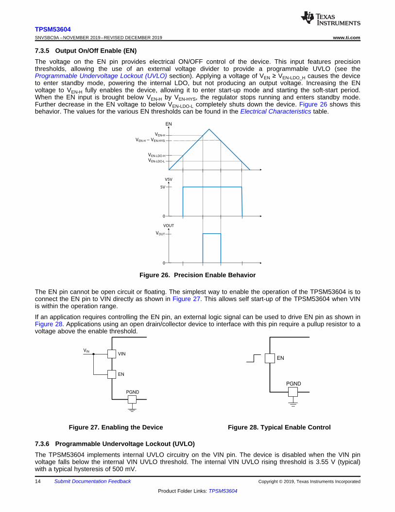
7.3.5 Output On/Off Enable (EN)The voltage on the EN pin provides electrical ON/OFF control of the device. This input features precisionthresholds, allowing the use of an external voltage divider to provide a programmable UVLO (see theProgrammable Undervoltage Lockout (UVLO) section). Applying a voltage of VEN ≥ VEN-LDO_H causes the deviceto enter standby mode, powering the internal LDO, but not producing an output voltage. Increasing the ENvoltage to VEN-H fully enables the device, allowing it to enter start-up mode and starting the soft-start period.When the EN input is brought below VEN-H by VEN-HYS, the regulator stops running and enters standby mode.Further decrease in the EN voltage to below VEN-LDO-L completely shuts down the device. Figure 26 shows thisbehavior. The values for the various EN thresholds can be found in the Electrical Characteristics table.
Figure 26. Precision Enable Behavior
The EN pin cannot be open circuit or floating. The simplest way to enable the operation of the TPSM53604 is toconnect the EN pin to VIN directly as shown in Figure 27. This allows self start-up of the TPSM53604 when VINis within the operation range.
If an application requires controlling the EN pin, an external logic signal can be used to drive EN pin as shown inFigure 28. Applications using an open drain/collector device to interface with this pin require a pullup resistor to avoltage above the enable threshold.
Figure 27. Enabling the Device Figure 28. Typical Enable Control
7.3.6 Programmable Undervoltage Lockout (UVLO)The TPSM53604 implements internal UVLO circuitry on the VIN pin. The device is disabled when the VIN pinvoltage falls below the internal VIN UVLO threshold. The internal VIN UVLO rising threshold is 3.55 V (typical)with a typical hysteresis of 500 mV.

VFB
PGOOD
107%105%
92%94%
High
Low
EN
VIN
RENT
AGND
VIN
RENB
15
TPSM53604www.ti.com SNVSBC9A –NOVEMBER 2019–REVISED DECEMBER 2019
Product Folder Links: TPSM53604
Submit Documentation FeedbackCopyright © 2019, Texas Instruments Incorporated
If an application requires a higher UVLO threshold, a resistor divider can be placed between VIN, the EN pin,and AGND as shown in Figure 29. The enable rising threshold (VEN-H) is 1.23 V (typ) with 100 mV (typ)hysteresis. Table 4 lists recommended resistor values for RENT and RENB to adjust the ULVO voltage.
To ensure proper start-up and reduce input current surges, TI recommends setting the UVLO threshold toapproximately 80% to 85% of the minimum expected input voltage.
Figure 29. Adjustable UVLO
Table 4. Resistor Values for Adjusting UVLOVIN UVLO (V) 6.5 10 15 20 25 30
RENT (kΩ) 100 100 100 100 100 100RENB (kΩ) 23.7 14.3 9.09 6.65 5.23 4.32
7.3.7 Power Good (PGOOD)The TPSM53604 has a built-in power-good signal (PGOOD) which indicates whether the output voltage is withinits regulation range. The PGOOD pin is an open-drain output that requires a pullup resistor to a nominal voltagesource of 18 V or less. The internal 5-V LDO output (V5V pin), can be used as the pullup voltage source. Atypical pull-up resistor value is between 10 kΩ and 100 kΩ. The maximum recommended PGOOD sink current is3 mA.
Once the output voltage rises above 94% of the set voltage, the PGOOD pin rises to the pullup voltage level.The PGOOD pin is pulled low when the output voltage drops lower than 92% or rises higher than 107% of thenominal set voltage. See Figure 30 for typical power-good thresholds.
Figure 30. Power-good Flag

Input Voltage (V)
Ou
tpu
t V
olt
ag
e (
V)
3.1 3.2 3.3 3.4 3.5 3.6 3.7 3.8 3.9 4 4.1 4.2
2.3
2.4
2.5
2.6
2.7
2.8
2.9
3
3.1
3.2
3.3
3.4
3.5
3.6
D041
IOUT
0 A
2 A
4 A
Input Voltage (V)
Sw
itc
hin
g F
req
ue
ncy
(kH
z)
3.5 3.6 3.7 3.8 3.9 4 4.1 4.2 4.3
600
700
800
900
1000
1100
1200
1300
1400
1500
D044
IOUT
2 A
4 A
16
TPSM53604SNVSBC9A –NOVEMBER 2019–REVISED DECEMBER 2019 www.ti.com
Product Folder Links: TPSM53604
Submit Documentation Feedback Copyright © 2019, Texas Instruments Incorporated
7.3.8 Light Load OperationIn light load conditions, the device turns on the high-side MOSFET until the inductor current reaches a controlledminimum value of approximately 1 A. As the input voltage decreases, reducing the voltage headroom betweenVIN and VOUT, the amount of time required to reach this minimum current increases. During this time, additionalenergy flows from VIN to VOUT, resulting in increased output voltage ripple. To eliminate this behavior, the ENUVLO function must be used to maintain at least 1 V of headroom above VOUT. Alternatively, additional outputcapacitance can be added to reduce the output voltage ripple in applications that operate at light loads with verylow VIN to VOUT headroom.
7.3.9 Voltage DropoutVoltage dropout is the difference between the input voltage and output voltage that is required to maintain outputvoltage regulation while providing the rated output current.
To ensure the TPSM53604 maintains output voltage regulation over the operating temperature range, theminimum VIN is 3.8 V or (VOUT + 1 V), whichever is greater.
The TPSM53604 operates in a frequency foldback mode when the dropout voltage is less than therecommendation above. Frequency foldback reduces the switching frequency to allow the output voltage tomaintain regulation as input voltage decreases. At light load, the TPSM53604 operates in PFM mode which is areduced frequency operation, see the Auto Mode section for more information on PFM mode. Figure 31 throughFigure 36 show typical dropout voltage and frequency foldback curves for 3.3 V, 5 V, and 7 V outputs at TA =25°C.
NOTEAs ambient temperature increases, dropout voltage and frequency foldback occur athigher input voltage.
VOUT = 3.3 V
Figure 31. Voltage Dropout
VOUT = 3.3 V
Figure 32. Frequency Foldback

Input Voltage (V)
Sw
itc
hin
g F
req
ue
ncy
(kH
z)
7.6 7.7 7.8 7.9 8 8.1 8.2
600
700
800
900
1000
1100
1200
1300
1400
1500
D046
IOUT
2 A
4 A
Input Voltage (V)
Ou
tpu
t V
olt
ag
e (
V)
6.5 6.6 6.7 6.8 6.9 7 7.1 7.2 7.3 7.4 7.5 7.6 7.7 7.8 7.9 8
5.7
5.8
5.9
6
6.1
6.2
6.3
6.4
6.5
6.6
6.7
6.8
6.9
7
7.1
7.2
D043
IOUT
0 A
2 A
4 A
Input Voltage (V)
Ou
tpu
t V
olt
ag
e (
V)
4.5 4.6 4.7 4.8 4.9 5 5.1 5.2 5.3 5.4 5.5 5.6 5.7 5.8
3.7
3.8
3.9
4
4.1
4.2
4.3
4.4
4.5
4.6
4.7
4.8
4.9
5
5.1
5.2
D042
IOUT
0 A
2 A
4 A
Input Voltage (V)
Sw
itc
hin
g F
req
ue
ncy
(kH
z)
5.4 5.5 5.6 5.7 5.8 5.9 6
600
700
800
900
1000
1100
1200
1300
1400
1500
D045
IOUT
2 A
4 A
17
TPSM53604www.ti.com SNVSBC9A –NOVEMBER 2019–REVISED DECEMBER 2019
Product Folder Links: TPSM53604
Submit Documentation FeedbackCopyright © 2019, Texas Instruments Incorporated
VOUT = 5 V
Figure 33. Voltage Dropout
VOUT = 5 V
Figure 34. Frequency Foldback
VOUT = 7 V
Figure 35. Voltage Dropout
VOUT = 7 V
Figure 36. Frequency Foldback
7.3.10 Overcurrent Protection (OCP)The TPSM53604 is protected from overcurrent conditions. Cycle-by-cycle current limit is used for overloads whilehiccup mode is used for short circuits. Hiccup mode is activated if a fault condition persists on the output. Hiccupmode reduces power dissipation under severe overcurrent conditions and prevents overheating and potentialdamage to the device. In hiccup mode, the regulator is shut down and kept off for 94 ms typical before theTPSM53604 tries to start again. If overcurrent or short-circuit fault condition still exist, hiccup repeats until thefault condition is removed. Once the fault is removed, the module automatically recovers with a normal soft-startpower up.
The typical current limit threshold for the TPSM53604 varies slightly as a function of input voltage and outputvoltage. Figure 37 shows the typical current limit threshold for several output voltages over the input voltagerange.

Input Voltage (V)
Ty
pic
al
Cu
rre
nt
Lim
it (
A)
0 5 10 15 20 25 30 35 40
4.0
4.2
4.4
4.6
4.8
5.0
5.2
5.4
5.6
5.8
D024
VOUT
1 V
1.8 V
3.3 V
5 V
7 V
18
TPSM53604SNVSBC9A –NOVEMBER 2019–REVISED DECEMBER 2019 www.ti.com
Product Folder Links: TPSM53604
Submit Documentation Feedback Copyright © 2019, Texas Instruments Incorporated
Figure 37. Current Limit Threshold
7.3.11 Thermal ShutdownThe internal thermal shutdown circuitry forces the device to stop switching if the junction temperature exceeds165°C typically. The device reinitiates the power-up sequence when the junction temperature drops below 148°Ctypically.

19
TPSM53604www.ti.com SNVSBC9A –NOVEMBER 2019–REVISED DECEMBER 2019
Product Folder Links: TPSM53604
Submit Documentation FeedbackCopyright © 2019, Texas Instruments Incorporated
7.4 Device Functional Modes
7.4.1 Active ModeThe TPSM53604 is in active mode when VIN is above the turn-on threshold and the EN pin voltage is above theEN high threshold. The most direct way to enable the TPSM53604 is to connect the EN pin to VIN. This allowsself start-up of the TPSM53604 when the input voltage is in the operation range of 3.8 V to 36 V. Connecting aresistor divider between VIN, EN, and AGND adjusts the UVLO to delay the turn on until VIN is closer to itsregulated voltage.
7.4.2 Auto ModeIn auto mode, the device moves between Pulse-Width Modulation (PWM) and Pulse-Frequency Modulation(PFM) as the load changes. At light loads, the regulator operates in PFM mode. At higher loads, the modechanges to PWM mode. The typical load current for which the device moves from PFM to PWM can be found inFigure 38 and Figure 39. The output current at which the device changes modes depends on the input voltageand the output voltage. For output currents above the curve, the device is in PWM mode. If the curve is a solidline, the PWM switching frequency is 1.4 MHz nominal. If the curve is a dashed line, the PWM switchingfrequency is reduced due to the minimum on-time of the internal controller to maintain output voltage regulation.For currents below the curves, the device is in PFM mode. For applications where the switching frequency mustbe known for a given condition, the above mentioned effects must be carefully tested before the design isfinalized.
In PWM mode, the regulator operates at a constant frequency using PWM to regulate the output voltage. Whileoperating in this mode, the output voltage is regulated by switching at a constant frequency and modulating theduty cycle to control the power to the load. This provides excellent line and load regulation and low outputvoltage ripple.
In PFM mode, the high-side MOSFET is turned on in a burst of one or more pulses to provide energy to the load.The duration of the burst and the actual switching frequency depends on the input voltage, output voltage, andload current. The frequency of these bursts is adjusted to regulate the output while diode emulation is used tomaximize efficiency. This mode provides high light-load efficiency by reducing the amount of input supply currentrequired to regulate the output voltage at small loads. However, in this mode, expect larger output voltage rippleand variable switching frequency.
Figure 38. PFM/PWM Thresholds (3.3 V, 5 V, and 7 V) Figure 39. PFM/PWM Thresholds (1 V and 1.8 V)
7.4.3 Shutdown ModeThe EN pin provides electrical ON and OFF control for the TPSM53604. When the EN pin voltage is below theEN low threshold, the device is in shutdown mode. In shutdown mode, the standby current is 5 μA typical.

VIN
PGND
VOUT
2.49 kO
FB
10 kO
PGOOD
EN
V5V
TPSM53604
AGND
VOUT = 5 V
47 µF
10 V
47 µF
10 V
VIN = 24 V
10 µF
50 V
100 kO
100 kO
10 µF
50 V
20
TPSM53604SNVSBC9A –NOVEMBER 2019–REVISED DECEMBER 2019 www.ti.com
Product Folder Links: TPSM53604
Submit Documentation Feedback Copyright © 2019, Texas Instruments Incorporated
8 Application and Implementation
NOTEInformation in the following applications sections is not part of the TI componentspecification, and TI does not warrant its accuracy or completeness. TI’s customers areresponsible for determining suitability of components for their purposes. Customers shouldvalidate and test their design implementation to confirm system functionality.
8.1 Application InformationThe TPSM53604 is a synchronous, step-down, DC/DC power module. It is used to convert a higher DC voltageto a lower DC voltage with a maximum output current of 4 A. The TPSM53604 can be configured in a negativeoutput voltage, inverting buck-boost (IBB) topology. For more details, see the Negative Output Voltage using theTPSM53602/3/4 application note. The following design procedure can be used to select components for theTPSM53604. Alternately, the WEBENCH® software can be used to generate complete designs. When generatinga design, the WEBENCH® software uses an iterative design procedure and accesses comprehensive databasesof components. See www.ti.com for more details.
8.2 Typical ApplicationThe TPSM53604 only requires a few external components to convert from a wide input voltage supply range to awide range of output voltages. Figure 40 shows a basic TPSM53604 schematic for a typical design.
Figure 40. TPSM53604 Typical Schematic
8.2.1 Design RequirementsFor this design example, use the parameters listed in Table 5 as the input parameters and follow the designprocedures in the Detailed Design Procedure section.
Table 5. Design Example ParametersDESIGN PARAMETER VALUE
Input voltage VIN 24 V typicalOutput voltage VOUT 5 VOutput current rating 4 A

RFBB =
(VOUT ± 1)(k )
10
21
TPSM53604www.ti.com SNVSBC9A –NOVEMBER 2019–REVISED DECEMBER 2019
Product Folder Links: TPSM53604
Submit Documentation FeedbackCopyright © 2019, Texas Instruments Incorporated
8.2.2 Detailed Design Procedure
8.2.2.1 Custom Design With WEBENCH® ToolsClick here to create a custom design using the TPSM53604 device with the WEBENCH® Power Designer.1. Start by entering the input voltage (VIN), output voltage (VOUT), and output current (IOUT) requirements.2. Optimize the design for key parameters such as efficiency, footprint, and cost using the optimizer dial.3. Compare the generated design with other possible solutions from Texas Instruments.
The WEBENCH Power Designer provides a customized schematic along with a list of materials with real-timepricing and component availability.
In most cases, these actions are available:• Run electrical simulations to see important waveforms and circuit performance• Run thermal simulations to understand board thermal performance• Export customized schematic and layout into popular CAD formats• Print PDF reports for the design, and share the design with colleagues
Get more information about WEBENCH tools at www.ti.com/WEBENCH.
8.2.2.2 Output Voltage SetpointThe output voltage of the TPSM53604 device is externally adjustable using a resistor divider. The recommendedvalue of RFBT is 10 kΩ. The value for RFBB can be selected from Table 1 or calculated using Equation 2:
(2)
For the desired output voltage of 5 V, the formula yields a value of 2.5 kΩ. Choose the closest available value of2.49 kΩ for RFBB.
8.2.2.3 Input CapacitorsThe TPSM53604 requires a minimum input capacitance of 20 µF (or 2 × 10 μF) ceramic type. High-qualityceramic type X5R or X7R capacitors with sufficient voltage rating are recommended. An additional 47 µF of non-ceramic capacitance is recommended for applications with transient load requirements. The voltage rating of theinput capacitors must be greater than the maximum input voltage.
For this design example, two 10-µF, 50-V, ceramic capacitors are used.
8.2.2.4 Output Capacitor SelectionThe TPSM53604 requires a minimum amount of output capacitance for proper operation. The minimum amountof required output varies depending on the output voltage. See Table 1 for the required output capacitance.
For this design example, two 47-µF, 10-V, ceramic capacitors are used.

VOUT
IOUT
VIN
EN
VOUT
PGOOD
VIN
EN
VOUT
PGOOD
22
TPSM53604SNVSBC9A –NOVEMBER 2019–REVISED DECEMBER 2019 www.ti.com
Product Folder Links: TPSM53604
Submit Documentation Feedback Copyright © 2019, Texas Instruments Incorporated
8.2.3 Application Curves
VIN = 24 V VOUT = 5 V COUT = 2 × 47 µF
Figure 41. Enable Turn-ON
VIN = 24 V VOUT = 5 V COUT = 2 × 47 µF
Figure 42. Enable Turn-OFF
VIN = 24 V VOUT = 5 V COUT = 2 × 47 µFIOUT = 1 A to 3 A Slew rate: 1 A/µs
Figure 43. Transient Response
9 Power Supply RecommendationsThe TPSM53604 is designed to operate from an input voltage supply range between 3.8 V and 36 V. This inputsupply must be well-regulated and able to withstand maximum input current and maintain a stable voltage. Theresistance of the input supply rail must be low enough that an input current transient does not cause a highenough drop at the TPSM53604 supply voltage that can cause a false UVLO fault triggering and system reset.
If the input supply is located more than a few centimeters from the TPSM53604, additional bulk capacitance canbe required in addition to the ceramic bypass capacitors. The typical amount of bulk capacitance is a 47-µFelectrolytic capacitor.

23
TPSM53604www.ti.com SNVSBC9A –NOVEMBER 2019–REVISED DECEMBER 2019
Product Folder Links: TPSM53604
Submit Documentation FeedbackCopyright © 2019, Texas Instruments Incorporated
10 LayoutThe performance of any switching power supply depends as much upon the layout of the PCB as the componentselection. The following guidelines help users design a PCB with the best power conversion performance,optimal thermal performance, and minimized generation of unwanted EMI.
10.1 Layout GuidelinesTo achieve optimal electrical and thermal performance, an optimized PCB layout is required. Figure 44 throughFigure 46 show a typical PCB layout. The following are some considerations for an optimized layout.• Use large copper areas for power planes (VIN, VOUT, and PGND) to minimize conduction loss and thermal
stress.• Place ceramic input and output capacitors close to the device pins to minimize high frequency noise.• Locate additional output capacitors between the ceramic capacitor and the load.• Connect AGND to PGND at a single point.• Place RFBT and RFBB as close as possible to the FB pin.• Use multiple vias to connect the power planes to internal layers.
10.2 Layout Examples
Figure 44. Typical Top-Layer Layout
Figure 45. Typical Layer-2 Layout

PCB Area (cm²)
Th
eta
JA
(°C
/W)
30 40 50 60 70 8018
19
20
21
22
23
24
D047
4-layer PCB
A(max)JA
D(max)
125 C T )R ( C / W)
PT
q q
(
24
TPSM53604SNVSBC9A –NOVEMBER 2019–REVISED DECEMBER 2019 www.ti.com
Product Folder Links: TPSM53604
Submit Documentation Feedback Copyright © 2019, Texas Instruments Incorporated
Layout Examples (continued)
Figure 46. Typical PGND Layer
10.3 Theta JA versus PCB AreaThe amount of PCB copper affects the thermal performance of the device. Figure 47 shows the effects of copperarea on the junction-to-ambient thermal resistance (RθJA) of the TPSM53604. The junction-to-ambient thermalresistance is plotted for a 4-layer PCB with PCB area from 30 cm2 to 80 cm2.
To determine the required copper area for an application:1. Determine the maximum power dissipation of the device in the application by referencing the power
dissipation graphs in sections Typical Characteristics (VIN = 5 V) through Typical Characteristics (VIN = 36 V).2. Calculate the maximum RθJA using Equation 3 and the maximum ambient temperature of the application.
(3)3. Reference Figure 47 to determine the minimum required PCB area for the application conditions.
Figure 47. RθJA versus PCB Area (per Layer)

25
TPSM53604www.ti.com SNVSBC9A –NOVEMBER 2019–REVISED DECEMBER 2019
Product Folder Links: TPSM53604
Submit Documentation FeedbackCopyright © 2019, Texas Instruments Incorporated
10.4 Package Specifications
TPSM53604 VALUE UNITWeight 429 mgFlammability Meets UL 94 V-OMTBF Calculated Reliability Per Bellcore TR-332, 50% stress, TA = 40°C, ground benign 89.3 MHrs
10.5 EMIThe TPSM53604 is compliant with EN55011 Class-B radiated emissions. Figure 48 and Figure 49 show typicalexamples of radiated emissions plots for the TPSM53604. The graphs include the plots of the antenna in thehorizontal and vertical positions.
EMI plots were measured using the standard TPSM53604EVM with no input filter.
Figure 48. Radiated Emissions 24-V Input, 5-V Output, 4-A Load

26
TPSM53604SNVSBC9A –NOVEMBER 2019–REVISED DECEMBER 2019 www.ti.com
Product Folder Links: TPSM53604
Submit Documentation Feedback Copyright © 2019, Texas Instruments Incorporated
EMI (continued)
Figure 49. Radiated Emissions 12-V Input, 5-V Output, 4-A Load

27
TPSM53604www.ti.com SNVSBC9A –NOVEMBER 2019–REVISED DECEMBER 2019
Product Folder Links: TPSM53604
Submit Documentation FeedbackCopyright © 2019, Texas Instruments Incorporated
11 Device and Documentation Support
11.1 Device Support
11.1.1 Third-Party Products DisclaimerTI'S PUBLICATION OF INFORMATION REGARDING THIRD-PARTY PRODUCTS OR SERVICES DOES NOTCONSTITUTE AN ENDORSEMENT REGARDING THE SUITABILITY OF SUCH PRODUCTS OR SERVICESOR A WARRANTY, REPRESENTATION OR ENDORSEMENT OF SUCH PRODUCTS OR SERVICES, EITHERALONE OR IN COMBINATION WITH ANY TI PRODUCT OR SERVICE.
11.1.2 Custom Design With WEBENCH® ToolsClick here to create a custom design using the TPSM53604 device with the WEBENCH® Power Designer.1. Start by entering the input voltage (VIN), output voltage (VOUT), and output current (IOUT) requirements.2. Optimize the design for key parameters such as efficiency, footprint, and cost using the optimizer dial.3. Compare the generated design with other possible solutions from Texas Instruments.
The WEBENCH Power Designer provides a customized schematic along with a list of materials with real-timepricing and component availability.
In most cases, these actions are available:• Run electrical simulations to see important waveforms and circuit performance• Run thermal simulations to understand board thermal performance• Export customized schematic and layout into popular CAD formats• Print PDF reports for the design, and share the design with colleagues
Get more information about WEBENCH tools at www.ti.com/WEBENCH.
11.2 Documentation Support
11.2.1 Related DocumentationFor related documentation see the following:
Texas Instruments, Negative Output Voltage Using the TPSM53602/3/4 application report
11.3 Receiving Notification of Documentation UpdatesTo receive notification of documentation updates, navigate to the device product folder on ti.com. In the upperright corner, click on Alert me to register and receive a weekly digest of any product information that haschanged. For change details, review the revision history included in any revised document.
11.4 Support ResourcesTI E2E™ support forums are an engineer's go-to source for fast, verified answers and design help — straightfrom the experts. Search existing answers or ask your own question to get the quick design help you need.
Linked content is provided "AS IS" by the respective contributors. They do not constitute TI specifications and donot necessarily reflect TI's views; see TI's Terms of Use.
11.5 TrademarksE2E is a trademark of Texas Instruments.WEBENCH is a registered trademark of Texas Instruments.All other trademarks are the property of their respective owners.
11.6 Electrostatic Discharge CautionThese devices have limited built-in ESD protection. The leads should be shorted together or the device placed in conductive foamduring storage or handling to prevent electrostatic damage to the MOS gates.

28
TPSM53604SNVSBC9A –NOVEMBER 2019–REVISED DECEMBER 2019 www.ti.com
Product Folder Links: TPSM53604
Submit Documentation Feedback Copyright © 2019, Texas Instruments Incorporated
11.7 GlossarySLYZ022 — TI Glossary.
This glossary lists and explains terms, acronyms, and definitions.
12 Mechanical, Packaging, and Orderable InformationThe following pages include mechanical packaging and orderable information. This information is the mostcurrent data available for the designated devices. This data is subject to change without notice and revision ofthis document. For browser-based versions of this data sheet, refer to the left-hand navigation.

PACKAGE OPTION ADDENDUM
www.ti.com 4-Jun-2020
Addendum-Page 1
PACKAGING INFORMATION
Orderable Device Status(1)
Package Type PackageDrawing
Pins PackageQty
Eco Plan(2)
Lead/Ball Finish(6)
MSL Peak Temp(3)
Op Temp (°C) Device Marking(4/5)
Samples
TPSM53604RDAR ACTIVE B3QFN RDA 15 1000 RoHS (InWork) & Green
NIPDAU Level-3-245C-168 HR -40 to 125 TPSM53604
(1) The marketing status values are defined as follows:ACTIVE: Product device recommended for new designs.LIFEBUY: TI has announced that the device will be discontinued, and a lifetime-buy period is in effect.NRND: Not recommended for new designs. Device is in production to support existing customers, but TI does not recommend using this part in a new design.PREVIEW: Device has been announced but is not in production. Samples may or may not be available.OBSOLETE: TI has discontinued the production of the device.
(2) RoHS: TI defines "RoHS" to mean semiconductor products that are compliant with the current EU RoHS requirements for all 10 RoHS substances, including the requirement that RoHS substancedo not exceed 0.1% by weight in homogeneous materials. Where designed to be soldered at high temperatures, "RoHS" products are suitable for use in specified lead-free processes. TI mayreference these types of products as "Pb-Free".RoHS Exempt: TI defines "RoHS Exempt" to mean products that contain lead but are compliant with EU RoHS pursuant to a specific EU RoHS exemption.Green: TI defines "Green" to mean the content of Chlorine (Cl) and Bromine (Br) based flame retardants meet JS709B low halogen requirements of <=1000ppm threshold. Antimony trioxide basedflame retardants must also meet the <=1000ppm threshold requirement.
(3) MSL, Peak Temp. - The Moisture Sensitivity Level rating according to the JEDEC industry standard classifications, and peak solder temperature.
(4) There may be additional marking, which relates to the logo, the lot trace code information, or the environmental category on the device.
(5) Multiple Device Markings will be inside parentheses. Only one Device Marking contained in parentheses and separated by a "~" will appear on a device. If a line is indented then it is a continuationof the previous line and the two combined represent the entire Device Marking for that device.
(6) Lead/Ball Finish - Orderable Devices may have multiple material finish options. Finish options are separated by a vertical ruled line. Lead/Ball Finish values may wrap to two lines if the finishvalue exceeds the maximum column width.
Important Information and Disclaimer:The information provided on this page represents TI's knowledge and belief as of the date that it is provided. TI bases its knowledge and belief on informationprovided by third parties, and makes no representation or warranty as to the accuracy of such information. Efforts are underway to better integrate information from third parties. TI has taken andcontinues to take reasonable steps to provide representative and accurate information but may not have conducted destructive testing or chemical analysis on incoming materials and chemicals.TI and TI suppliers consider certain information to be proprietary, and thus CAS numbers and other limited information may not be available for release.
In no event shall TI's liability arising out of such information exceed the total purchase price of the TI part(s) at issue in this document sold by TI to Customer on an annual basis.

www.ti.com
PACKAGE OUTLINE
5.14.9
5.65.4
4.1 MAX
2.6 TYP
8X 0.65
2X 0.725
1.43
2X 0.975
2.5 0.05
2.5 0.05
4.6 0.05
2X1.5 0.05
3X 1.31.1
10X 0.60.4 1.3
1.1
4X 0.60.4
10X 0.450.25
(0.16) TYP
B3QFN - 4.1 mm max heightRDA0015APLASTIC QUAD FLATPACK - NO LEAD
4224086/C 03/2019
NOTES: 1. All linear dimensions are in millimeters. Any dimensions in parenthesis are for reference only. Dimensioning and tolerancing per ASME Y14.5M. 2. This drawing is subject to change without notice. 3. The package thermal pad must be soldered to the printed circuit board for optimal thermal and mechanical performance.
PIN 1 INDEX AREA
0.08 C
SEATING PLANE
PKG
PKG
0.1 C A B0.05 C
0.1 C A B0.05 C
1
78
14
15
PIN 1 ID
SCALE 1.800
AB
C

www.ti.com
EXAMPLE BOARD LAYOUT
0.05 MAXALL AROUND
0.05 MINALL AROUND
(4.7)
2X (4)
(1) TYP
(1)TYP
(4.6)
(2.5)
(1.5)
(2.5)
4X (1.4)4X (0.5)
10X (0.7)
10X (0.35)
2X (1.43)
8X (0.65)
2X (0.725)
2X (0.975)
(R0.05) TYP
( 0.2) VIATYP
B3QFN - 4.1 mm max heightRDA0015APLASTIC QUAD FLATPACK - NO LEAD
4224086/C 03/2019
NOTES: (continued) 4. This package is designed to be soldered to a thermal pad on the board. For more information, see Texas Instruments literature number SLUA271 (www.ti.com/lit/slua271).5. Vias are optional depending on application, refer to device data sheet. If any vias are implemented, refer to their locations shown on this view. It is recommended that vias under paste be filled, plugged or tented.
LAND PATTERN EXAMPLEEXPOSED METAL SHOWN
SCALE: 16X
1
7
8
14
15
PKG
PKG
SCALE 30.000SOLDER MASK DETAILS
EXPOSEDMETAL
METAL EDGESOLDER MASKOPENING
EXPOSEDMETAL
SOLDER MASKOPENING METAL UNDER
SOLDER MASK
NON SOLDER MASKDEFINED
SOLDER MASK DEFINED

www.ti.com
EXAMPLE STENCIL DESIGN
10X (0.65)
10X (0.3)
4X (0.6)
4X(0.65)
4X(0.95)
4X (0.475)
2X (4)
(4.7)
2X (0.975)
4X (1.35)4X (0.45)
2X (1.43)
8X (0.65)
2X (0.725)
(R0.05) TYP
4X(1.15)
4X (0.425)
4X (1.675)
4X (0.625)
B3QFN - 4.1 mm max heightRDA0015APLASTIC QUAD FLATPACK - NO LEAD
4224086/C 03/2019
NOTES: (continued) 6. Laser cutting apertures with trapezoidal walls and rounded corners may offer better paste release. IPC-7525 may have alternate design recommendations.
SOLDER PASTE EXAMPLEBASED ON 0.125 mm THICK STENCIL
EXPOSED PAD 15:
56% PRINTED SOLDER COVERAGE BY AREASCALE: 16X
PKG
1
78
14
15
PKG

IMPORTANT NOTICE AND DISCLAIMER
TI PROVIDES TECHNICAL AND RELIABILITY DATA (INCLUDING DATASHEETS), DESIGN RESOURCES (INCLUDING REFERENCE DESIGNS), APPLICATION OR OTHER DESIGN ADVICE, WEB TOOLS, SAFETY INFORMATION, AND OTHER RESOURCES “AS IS” AND WITH ALL FAULTS, AND DISCLAIMS ALL WARRANTIES, EXPRESS AND IMPLIED, INCLUDING WITHOUT LIMITATION ANY IMPLIED WARRANTIES OF MERCHANTABILITY, FITNESS FOR A PARTICULAR PURPOSE OR NON-INFRINGEMENT OF THIRD PARTY INTELLECTUAL PROPERTY RIGHTS.These resources are intended for skilled developers designing with TI products. You are solely responsible for (1) selecting the appropriate TI products for your application, (2) designing, validating and testing your application, and (3) ensuring your application meets applicable standards, and any other safety, security, or other requirements. These resources are subject to change without notice. TI grants you permission to use these resources only for development of an application that uses the TI products described in the resource. Other reproduction and display of these resources is prohibited. No license is granted to any other TI intellectual property right or to any third party intellectual property right. TI disclaims responsibility for, and you will fully indemnify TI and its representatives against, any claims, damages, costs, losses, and liabilities arising out of your use of these resources.TI’s products are provided subject to TI’s Terms of Sale (www.ti.com/legal/termsofsale.html) or other applicable terms available either on ti.com or provided in conjunction with such TI products. TI’s provision of these resources does not expand or otherwise alter TI’s applicable warranties or warranty disclaimers for TI products.
Mailing Address: Texas Instruments, Post Office Box 655303, Dallas, Texas 75265Copyright © 2020, Texas Instruments Incorporated