transmission line network for multi-ghz clock distribution hongyu chen and chung-kuan cheng...
TRANSCRIPT

Transmission Line Network For Multi-GHz Clock
Distribution
Hongyu Chen and Chung-Kuan Cheng
Department of Computer Science and Engineering, University of California, San
Diego
January 2005

Outline Introduction Problem formulation Skew reduction effect of
transmission line shunts Optimal sizing of multilevel
network Experimental results

Motivation Clock skew caused by parameter
variations consumes increasingly portion of clock period in high speed circuits
RC shunt effect diminishes in multiple-GHz range
Transmission line can lock the periodical signals
Difficult to analysis and synthesis network with explicit non-linear feedback path

Related Work (I)Phase
Detector s
asG
PullableVCO
PullableVCO
C0
C1
… … …
PullableVCO
Cn
ReferenceClock
I. Galton, D. A. Towne, J. J. Rosenberg, and H. T. Jensen, “Clock Distribution Using Coupled Oscillators,” in Prof. of ISCAS 1996, vol. 3, pp.217-220
•Transmission line shunts with less than quarter wavelength long can lock the RC oscillators both in
phase and magnitude

Related work (II)
V. Gutnik and A. P. Chandraksan, “Active GHz Clock Network Using Distributed PLLs,” in IEEE Journal of Solid-State Circuits, pp. 1553-1560, vol. 35, No. 11, Nov. 2000
• Active feedback path using distributed PLLs
• Provable stability under certain conditions

Related work (III)
F. O’Mahony, C. P. Yue, M. A. Horowitz, and S. S. Wong, “Design of a 10GHz Clock Distribution Network Using
Coupled Standing-Wave Oscillators,” in Proc. of DAC, pp. 682-687, June 2003
• Combined clock generation and distribution using standing wave oscillator
• Placing lamped transconductors along the wires to compensate wire loss

Related work (IV)
J. Wood, et al., “Rotary Traveling-Wave Oscillator Arrays: A New Clock Technology” in IEEE JSSC, pp. 1654-1665, Nov.
2001
• Clock signals generated by traveling waves
• The inverter pairs compensate the resistive loss and ensure square waveform

Our contributions Theoretical study of the
transmission line shunt behavior, derive analytical skew equation
Propose multi-level spiral network for multi-GHz clock distribution
Convex programming technique to optimize proposed multi-level network. The optimized network achieves below 4ps skew for 10GHz rate

Problem Formulation Inductance diminishes shunt effect Transmission line shunts with
proper tailored length can reduce skew
Differential sine waves Variation model Hybrid h-tree and shunt network Problem statement

Inductance Diminishes Shunt Effects
Vs1 Rs
C
Vs2 Rs
C
R
1
2
u(t)
u(t-T)
L
f(GHz) 0.5 1 1.5 2 3 3.5 4 5
skew(ps)
3.9 4.2 5.8 7.5 9.9 13 17 26
• 0.5um wide 1.2 cm long copper wire
• Input skew 20ps

Wavelength Long Transmission Line Synchronizes Two Sources
Rs Rs
)sin(2
t
U s
)sin(1
t
U s
1 2

Differential Sine Waves Sine wave form simplifies the
analysis of resonance phenomena of the transmission line
Differential signals improve the predictability of inductance value
Can convert the sine wave to square wave at each local region

Model of parameter variations
Process variations Variations on wire width and transistor
length Linear variation model d = d0 + kx x+ky y
Supply voltage fluctuations Random variation (10%)
Easy to change to other more sophisticated variation models in our design framework

Multilevel Transmission Line Spiral Network
(a) H-tree (b) Spirals driven by H-tree
clock drivers

Problem Statement Formulation A:Given: model of parameter variationsInput: H-tree and n-level spiral networkConstraint: total routing areaObject function: minimize skew
Output: optimal wire width of each level spiral Formulation B:Constraint: skew toleranceObject function: minimize total routing area

Skew Reduction Effect of Transmission Line Shunts Two sources case
Circuit model and skew expression Derivation of skew function Spice validation
Multiple sources case Random skew model Skew expression Spice validation

Transmission line Shunt with Two Sources
Rs Rs
)sin(2
t
U s
)sin(1
t
U s
1 2
L
R
L
R
e
e
1
1
• Transmission Line with exact multiple wave length long
• Large driving resistance to increase reflection

Spice Validation of Skew Equation

Multiple Sources Case
L
R
L
R
e
e3
3
1
1
Random model:
• Infinity long wire
• Input phases uniformly distribution on [0, Φ]

Configuration of Wires
Ground
CLK+ CLK-2um
3.5 um
w w
240nm
• Coplanar copper transmission line
• height: 240nm, separation: 2um, distance to ground: 3.5um, width(w): 0.5 ~ 40um
• Use Fasthenry to extract R,L
• Linear R/L~w Relation
• R/L = a/w+b

Optimal Sizing of Spiral Wires
Lemma: is a convex function on , where, k is a positive constant.
wk
wk
ce
cewf
/
/
1
1)(
),2
[ k
w
n
n
n
n
i
i
i
i
w
k
n
w
k
nn
w
k
w
k
w
k
w
k
ec
ec
ec
ec
ec
ec
1
1))...
1
1))
1
1((( 3
2
22
1
11
2
2
2
2
Awln
iii
1
),...,2,1(, nimw ii
Min:
S.t.:
• Impose the minimal wire width constraint for each level spiral, such that the cost function is convex

Optimal Sizing of Spiral Wires
Theorem: The local optimum of the previous mathematical programming is the global optimum.
Many numerical methods (e.g. gradient descent) can solve the problem
We use the OPT-toolkit of MATLAB to solve the problem

Experimental Results Set chip size to 2cm x 2cm Clock frequency 10.336GHz Synthesize H-tree using P-tree algorithm Set the initial skew at each level using
SPICE simulation results under our variation model
Use FastHenry and FastCap to extract R,L,C value
Use W-elements in HSpice to simulate the transmissionlin
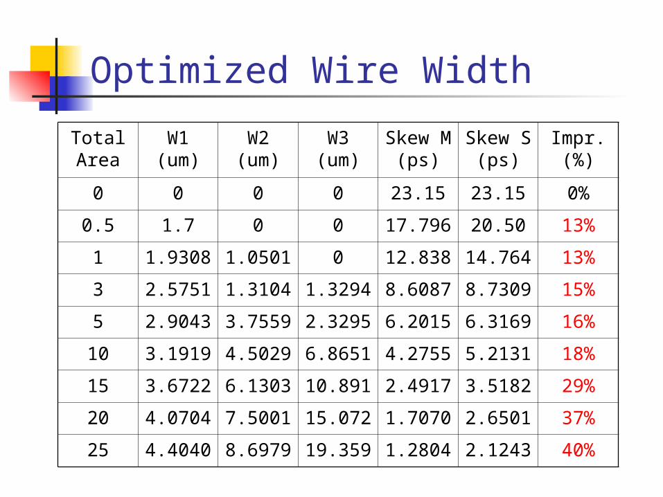
Optimized Wire Width
Total Area
W1 (um)
W2 (um)
W3 (um)
Skew M (ps)
Skew S (ps)
Impr.(%)
0 0 0 0 23.15 23.15 0%
0.5 1.7 0 0 17.796 20.50 13%
1 1.9308 1.0501 0 12.838 14.764 13%
3 2.5751 1.3104 1.3294 8.6087 8.7309 15%
5 2.9043 3.7559 2.3295 6.2015 6.3169 16%
10 3.1919 4.5029 6.8651 4.2755 5.2131 18%
15 3.6722 6.1303 10.891 2.4917 3.5182 29%
20 4.0704 7.5001 15.072 1.7070 2.6501 37%
25 4.4040 8.6979 19.359 1.2804 2.1243 40%

Simulated Output Voltages
Transient response of 16 nodes on transmission line
Signals synchronized in 10 clock cycles

Simulated Output voltages
Steady state response: skew reduced from 8.4ps to 1.2ps

Power Consumption
Area 3 4 5 7 10 15 20 25
PM(mw) 0.4 0.5 0.7 0.9 1.0 1.4 1.5 1.6
PS(mw) 0.83 1.5 2.1 2.64 3.04 4.7 7.2 8.3
reduce(%)
48 67 67 66 67 70 79 81
PM: power consumption of multilevel meshPS: power consumption of single level mesh

Area Skew-S Skew-MAve. Worst Ave. Worst Impr(%)
0 28.4 36.5 28.4 36.5 0%3 9.75 12.33 8.75 9.07 11%5 7.32 9.06 6.55 6.91 12%
10 6.31 805 4.41 5.41 30%15 5.03 7.33 2.81 4.93 44%25 3.83 4.61 1.72 3.06 55%
Skew with supply fluctuation

Conclusion and Future Directions Transmission line shunts
demonstrate its unique potential of achieving low skew low jitter global clock distribution under parameter variations
Future Directions Exploring innovative topologies of
transmission line shunts Design clock repeaters and generators Actual layout and fabrication of test chip
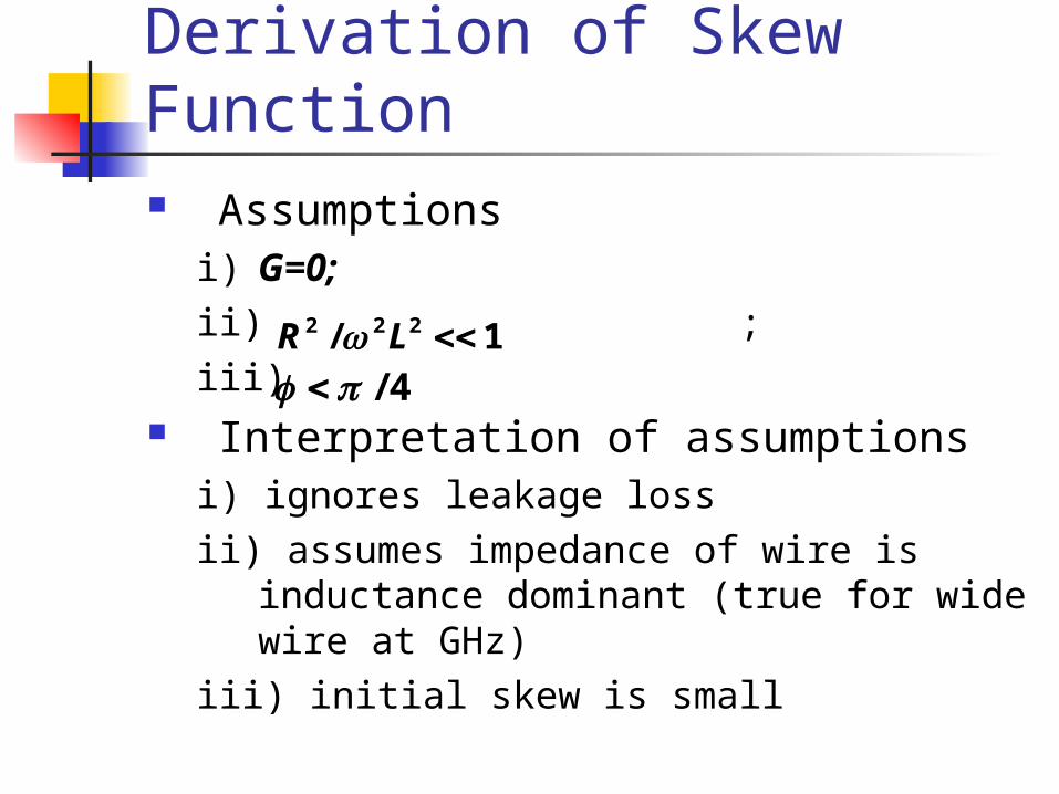
Derivation of Skew Function Assumptions
i) G=0;
ii) ;iii)
Interpretation of assumptionsi) ignores leakage lossii) assumes impedance of wire is
inductance dominant (true for wide wire at GHz)
iii) initial skew is small
1/ 222 LR 4/

Derivation of Skew Function
1,1V1,2V
2,2V
2,1V 1V
2V
1
2Vi,j : Voltage of node 1
caused by source Vsj
independently
Φ : Initial phase shift (skew)
:
Resulted skew
• Loss causes skew
• Lossless line: V1,2
=V2,2 , V2,1 =V1,1 Zero skew
12
V
V
2
1
2,21,2
2,11,1
VV
VV

Derivation of Skew Function
• Summing up all the incoming and reflected waveforms to get Vi,j
• Using first order Taylor expansion
and
to simplify the derivation
• Utilizing the geometrical relation in the previous figure, we get
xx sin xe x 1
L
R
L
R
e
e
1
1