tuning the threshold voltage of carbon nanotube transistors by n
TRANSCRIPT

Tuning the threshold voltage of carbon nanotubetransistors by n-type molecular doping for robustand flexible complementary circuitsHuiliang Wanga,1, Peng Weib,1, Yaoxuan Lic, Jeff Hanb, Hye Ryoung Leec, Benjamin D. Naabd, Nan Liub,Chenggong Wange, Eric Adijantob, Benjamin C.-K. Teec, Satoshi Morishitab, Qiaochu Lib, Yongli Gaoe, Yi Cuia,and Zhenan Baob,2
Departments of aMaterials Science and Engineering, bChemical Engineering, cElectrical Engineering, and dChemistry, Stanford University, Stanford, CA 94305;and eDepartment of Physics and Astronomy, University of Rochester, Rochester, NY 14627
Edited by Peidong Yang, University of California, Berkeley, CA, and accepted by the Editorial Board February 18, 2014 (received for review November 3, 2013)
Tuning the threshold voltage of a transistor is crucial for realizingrobust digital circuits. For silicon transistors, the threshold voltagecan be accurately controlled by doping. However, it remainschallenging to tune the threshold voltage of single-wall nanotube(SWNT) thin-film transistors. Here, we report a facile method tocontrollably n-dope SWNTs using 1H-benzoimidazole derivativesprocessed via either solution coating or vacuum deposition. Thethreshold voltages of our polythiophene-sorted SWNT thin-filmtransistors can be tuned accurately and continuously over a widerange. Photoelectron spectroscopy measurements confirmed thatthe SWNT Fermi level shifted to the conduction band edge withincreasing doping concentration. Using this doping approach, weproceeded to fabricate SWNT complementary inverters by inkjetprinting of the dopants. We observed an unprecedented noise mar-gin of 28 V at VDD = 80 V (70% of 1/2VDD) and a gain of 85. Addi-tionally, robust SWNT complementary metal−oxide−semiconductorinverter (noise margin 72% of 1/2VDD) and logic gates with rail-to-rail output voltage swing and subnanowatt power consumptionwere fabricated onto a highly flexible substrate.
nanomaterials | n-doping | inkjet-printed | CMOS circuit
Flexible electronics have attracted increasing attention recentlydue to the plethora of possible and realized applications in
radio-frequency identification cards (1, 2), flexible displays (3, 4),and digital processors (5). Solution-processed single-walled car-bon nanotubes (SWNTs) are a promising candidate for flexiblecircuits due to their high charge carrier mobility (6), excellentflexibility/stretchability (7–9), and their compatibility with low-cost, large-area manufacturing processes, such as printing (1, 10)of SWNTs. Their applications in thin-film transistors (TFTs)and integrated logic circuits (11–14) have been demonstrated.However, to achieve robust digital circuits with high immunityagainst the influence of electronic noise in the system, it is im-portant to be able to control the specific value of the thresholdvoltage of a transistor during the fabrication process (15, 16).This is because transistor threshold voltage determines the in-put voltage at which a circuit switches between two logic states(trip voltage of an inverter). When the trip voltage is half of thesupply voltage, the circuit has the largest noise margin, which isa quantitative measure of the immunity of a logic circuit againstnoise and a figure of merit to characterize the robustness ofthe circuit (17, 18). If threshold voltage cannot be controlledduring the fabrication process, the resulting circuit might notwork reliably due to the electrical noise that is always present inthe system.Because SWNTs have ambipolar electrical transport proper-
ties (19), accurately tuning the threshold voltage permits the con-struction of complementary metal−oxide−semiconductor (CMOS)circuits that use both the p-type and n-type character of SWNTs.The advantages of CMOS circuits compared with unipolar logic
circuits include lower power consumption, simpler circuit design,higher noise margin, better tolerance to the spread of thresholdvoltages of the transistors, and consequently higher circuit yields(15–17). Several approaches have been reported to adjust thethreshold voltage of SWNTs and enable n-type SWNT transistors,including the use of (i): low-work function metal as source/draincontacts (20–22), (ii) atomic layer deposited (ALD) high-κ oxideon the SWNTs (23), and (iii) chemical doping on either thecontacts or the bulk of SWNTs (14, 24–32). However, the con-tinuous and reliable tuning of the threshold voltage of SWNTTFTs has not been achieved, thereby hindering optimal SWNTcircuit performance. In addition, although several groups havefabricated flexible (11, 12, 13) SWNT unipolar circuits, the fab-rication of SWNT CMOS electronics on a flexible substrate hasyet to be reported.We recently described the use of dimethyl-dihydro-benzoimi-
dazoles (DMBI) as a highly efficient class of molecular dopantsfor [6,6]-phenyl-C61-butyric acid methyl ester (PCBM), C60, andgraphene (33–35). Because these dopants can be depositedvia solution processing, their use can be envisioned in large-area printable electronics. We have also developed a simpleand scalable SWNT sorting method using regioregular poly(3-dodecylthiophene) (rr-P3DDT) to achieve highly selectivedispersion of semiconducting SWNTs (36, 37). As a result, the
Significance
Highly noise-resistant logic gates are needed for large-scalecircuits. This was challenging previously with carbon nanotubecircuits due to the lack of control of the threshold voltages ofnanotube transistors. We demonstrate the use of dopants totune the charge carrier density of carbon nanotubes films andhence precisely control the threshold voltages of carbonnanotube transistors. This doping method is highly versatileand can be applied through inkjet printing. With this tech-nique, we demonstrate highly noise-resistant and low powerconsumption carbon nanotube logic gates on a flexible sub-strate. This work places carbon nanotubes in a highly com-petitive position for large-scale solution-processed flexiblecircuits.
Author contributions: H.W., P.W., and Z.B. designed research; H.W., P.W., Y.L., J.H., H.R.L.,B.D.N., N.L., C.W., E.A., B.C.-K.T., S.M., and Q.L. performed research; H.W., Y.L., H.R.L.,C.W., Y.G., and Y.C. contributed new reagents/analytic tools; H.W., P.W., Y.L., J.H., C.W.,and Z.B. analyzed data; and H.W., P.W., and Z.B. wrote the paper.
The authors declare no conflict of interest.
This article is a PNAS Direct Submission. P.Y. is a guest editor invited by the EditorialBoard.1H.W. and P.W. contributed equally to this work.2To whom correspondence should be addressed. E-mail: [email protected].
This article contains supporting information online at www.pnas.org/lookup/suppl/doi:10.1073/pnas.1320045111/-/DCSupplemental.
4776–4781 | PNAS | April 1, 2014 | vol. 111 | no. 13 www.pnas.org/cgi/doi/10.1073/pnas.1320045111
polymer-sorted SWNT network TFTs exhibited a very high yieldand good uniformity across large areas (38).In this work, we demonstrate the effective n-type doping of
our rr-P3DDT sorted SWNT films using DMBI dopants, via bothvacuum and solution deposition methods. By controlling thedopant concentration or thickness, we can accurately tune thecharge carrier density of SWNT films and consequently the de-vice threshold voltages over a wide range. As a result, both then-type and p-type SWNT transistors with symmetric thresholdvoltages and current outputs can be fabricated. We have alsoused photoelectron spectroscopy (PES) to observe the Fermilevel shifts of the SWNTs after n-doping. The controlled n-typedoping of SWNTs enabled us to fabricate inverters with inkjet-printed dopants that had unprecedented noise margins as high as28 V at VDD = 80V (70% of 1/2VDD) and gains up to 85. Fur-thermore, the versatility of our n-type doping method allowedus to fabricate flexible SWNT CMOS inverters, negated AND(NAND) and negated OR (NOR) logic gates. The flexible CMOSinverter also demonstrated robust operation with an even highernoise margin of 1.8 V at VDD = 5 V (72% of 1/2VDD) and a gain of18. The flexible CMOS NAND and NOR logic gates demon-strated a record rail-to-rail output voltage swings and sub-nanowatt static power consumption.
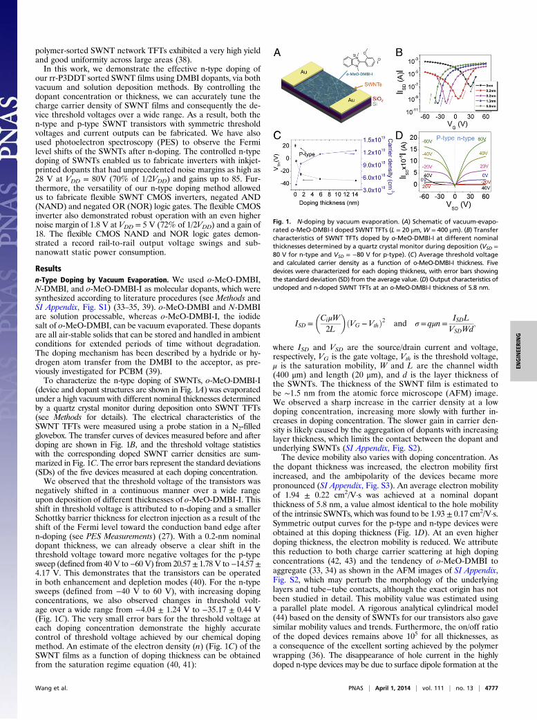
Resultsn-Type Doping by Vacuum Evaporation. We used o-MeO-DMBI,N-DMBI, and o-MeO-DMBI-I as molecular dopants, which weresynthesized according to literature procedures (see Methods andSI Appendix, Fig. S1) (33–35, 39). o-MeO-DMBI and N-DMBIare solution processable, whereas o-MeO-DMBI-I, the iodidesalt of o-MeO-DMBI, can be vacuum evaporated. These dopantsare all air-stable solids that can be stored and handled in ambientconditions for extended periods of time without degradation.The doping mechanism has been described by a hydride or hy-drogen atom transfer from the DMBI to the acceptor, as pre-viously investigated for PCBM (39).To characterize the n-type doping of SWNTs, o-MeO-DMBI-I
(device and dopant structures are shown in Fig. 1A) was evaporatedunder a high vacuum with different nominal thicknesses determinedby a quartz crystal monitor during deposition onto SWNT TFTs(see Methods for details). The electrical characteristics of theSWNT TFTs were measured using a probe station in a N2-filledglovebox. The transfer curves of devices measured before and afterdoping are shown in Fig. 1B, and the threshold voltage statisticswith the corresponding doped SWNT carrier densities are sum-marized in Fig. 1C. The error bars represent the standard deviations(SDs) of the five devices measured at each doping concentration.We observed that the threshold voltage of the transistors was
negatively shifted in a continuous manner over a wide rangeupon deposition of different thicknesses of o-MeO-DMBI-I. Thisshift in threshold voltage is attributed to n-doping and a smallerSchottky barrier thickness for electron injection as a result of theshift of the Fermi level toward the conduction band edge aftern-doping (see PES Measurements) (27). With a 0.2-nm nominaldopant thickness, we can already observe a clear shift in thethreshold voltage toward more negative voltages for the p-typesweep (defined from 40 V to−60 V) from 20.57± 1.78 V to −14.57±4.17 V. This demonstrates that the transistors can be operatedin both enhancement and depletion modes (40). For the n-typesweeps (defined from −40 V to 60 V), with increasing dopingconcentrations, we also observed changes in threshold volt-age over a wide range from −4.04 ± 1.24 V to −35.17 ± 0.44 V(Fig. 1C). The very small error bars for the threshold voltage ateach doping concentration demonstrate the highly accuratecontrol of threshold voltage achieved by our chemical dopingmethod. An estimate of the electron density (n) (Fig. 1C) of theSWNT films as a function of doping thickness can be obtainedfrom the saturation regime equation (40, 41):
ISD =�CiμW2L
�ðVG −VthÞ2 and σ = qμn=
ISDLVSDWd
;
where ISD and VSD are the source/drain current and voltage,respectively, VG is the gate voltage, Vth is the threshold voltage,μ is the saturation mobility, W and L are the channel width(400 μm) and length (20 μm), and d is the layer thickness ofthe SWNTs. The thickness of the SWNT film is estimated tobe ∼1.5 nm from the atomic force microscope (AFM) image.We observed a sharp increase in the carrier density at a lowdoping concentration, increasing more slowly with further in-creases in doping concentration. The slower gain in carrier den-sity is likely caused by the aggregation of dopants with increasinglayer thickness, which limits the contact between the dopant andunderlying SWNTs (SI Appendix, Fig. S2).The device mobility also varies with doping concentration. As
the dopant thickness was increased, the electron mobility firstincreased, and the ambipolarity of the devices became morepronounced (SI Appendix, Fig. S3). An average electron mobilityof 1.94 ± 0.22 cm2/V·s was achieved at a nominal dopantthickness of 5.8 nm, a value almost identical to the hole mobilityof the intrinsic SWNTs, which was found to be 1.93 ± 0.17 cm2/V·s.Symmetric output curves for the p-type and n-type devices wereobtained at this doping thickness (Fig. 1D). At an even higherdoping thickness, the electron mobility is reduced. We attributethis reduction to both charge carrier scattering at high dopingconcentrations (42, 43) and the tendency of o-MeO-DMBI toaggregate (33, 34) as shown in the AFM images of SI Appendix,Fig. S2, which may perturb the morphology of the underlyinglayers and tube−tube contacts, although the exact origin has notbeen studied in detail. This mobility value was estimated usinga parallel plate model. A rigorous analytical cylindrical model(44) based on the density of SWNTs for our transistors also gavesimilar mobility values and trends. Furthermore, the on/off ratioof the doped devices remains above 105 for all thicknesses, asa consequence of the excellent sorting achieved by the polymerwrapping (36). The disappearance of hole current in the highlydoped n-type devices may be due to surface dipole formation at the
Fig. 1. N-doping by vacuum evaporation. (A) Schematic of vacuum-evapo-rated o-MeO-DMBI-I doped SWNT TFTs (L = 20 μm, W = 400 μm). (B) Transfercharacteristics of SWNT TFTs doped by o-MeO-DMBI-I at different nominalthicknesses determined by a quartz crystal monitor during deposition (VSD =80 V for n-type and VSD = −80 V for p-type). (C) Average threshold voltageand calculated carrier density as a function of o-MeO-DMBI-I thickness. Fivedevices were characterized for each doping thickness, with error bars showingthe standard deviation (SD) from the average value. (D) Output characteristics ofundoped and n-doped SWNT TFTs at an o-MeO-DMBI-I thickness of 5.8 nm.
Wang et al. PNAS | April 1, 2014 | vol. 111 | no. 13 | 4777
ENGINEE
RING

metal−SWNT contact that suppresses hole injection (28). Wenote that the n-doped devices are not air-stable. However,devices exposed to air can recover completely when they arereturned to nitrogen atmosphere, as shown in SI Appendix, Fig.S4. We also observed hysteresis in our n-doped device (SI Ap-pendix, Fig. S5), but the magnitude of the hysteresis is not largerthan the hysteresis in our p-type devices (SI Appendix, Fig. S6);encapsulation with inorganic or organic layers is expected toimprove air stability and reduce the hysteresis of the SWNTTFTs (45, 46).
n-Type Doping by Solution Processing. For solution processing,o-MeO-DMBI and N-DMBI were used (chemical structuresshown in Fig. 2A) as the n-type dopants. They are both highlysoluble in common solvents suitable for spin coating and inkjetprinting. Different dopant concentrations in ethanol weredeposited on the SWNT TFTs via spin coating (see Methods).The transfer curves after doping by o-MeO-DMBI and N-DMBI are shown in Fig. 2B and Fig. 2C, respectively, and thestatistics of the threshold voltage shift and the calculated carrierdensity with respect to the doping concentration for both dopantsare shown in Fig. 2D and SI Appendix, Fig. S7, respectively. Therange of the n-type threshold voltage shift for the o-MeO-DMBIdoped devices is from 6.61 ± 2.73 V at 1 mg/mL to as low as −31.22±0.87 V at 25 mg/mL The changes in performance and morphology(SI Appendix, Figs. S8−S10) at different concentrations are similarto those observed with vacuum-evaporated o-MeO-DMBI-I atdifferent thicknesses. The best performing o-MeO-DMBI dopeddevices were obtained at 10 mg/mL with an average electronmobility of 1.58 ± 0.37 cm2/V·s and a high average on/off ratio of(1.08 ± 0.91) × 105.In contrast, N-DMBI showed a much stronger n-doping ef-
fect. At a concentration of 1 mg/mL, for instance, the thresh-old voltage already shifted to −20.21 ± 1.69 V. The mobilityincreased to as high as 27.50 ± 5.20 cm2/V·s at a solutionconcentration of 25 mg/mL (SI Appendix, Fig. S8). However,the on/off ratio was greatly reduced due to a significant increase inthe off current, which was also observed for our previously reported
n-doped PC61BM transistors (33, 34). Hence, while N-DMBI is aneffective n-type dopant, it is difficult to independently controlboth threshold voltage and on/off ratio due to the high dopingefficiency observed for N-DMBI dopants, thereby limiting itsutility in digital circuits. However, N-DMBI could be very usefulfor analog or radio frequency applications, which require a highmobility but tolerate a much lower on/off ratio than digitalcircuits.
Fermi Level Shift upon n-Doping. The relationship between theshift of the threshold voltage and the electron carrier density ofn-doped SWNTs was explored with PES. Specifically, the Fermilevel shift was determined at different doping concentrations.From the PES spectra shown in Fig. 3A, we observed an increasein work function from the undoped to doped SWNT films. Afterdoping with 1 mg/mL o-MeO-DMBI solution, the work function ofSWNTs decreased from 4.98 eV for the undoped sample to 4.30 eV,indicating an effective interfacial electron transfer from o-MeO-DMBI to SWNTs. The doped SWNTs with 3-nm o-MeO-DMBI-Ifilms showed a similar decrease of work function to 4.22 eV. Ata higher doping concentration obtained with 25 mg/mL o-MeO-DMBI solution, the work function of the doped SWNTs was lowerthan 4.00 eV, demonstrating the strong increase in electron densitywith these n-type dopants. Although it has been reported that theshift of threshold voltage during potassium doping of individualSWNTs might be due to the modification of the metal contacts bylowering the Schottky barrier height for electron injection (28), thereduction in work function shown in our PES measurements indi-cates that it is indeed the doping of the SWNT films that caused theshift of the threshold voltage. The reduction in barrier thickness forelectron injection with increase in n-doping is shown schematicallyin Fig. 3B.
Complementary Inverters with Inkjet Printed n-Dopant. The con-trolled tuning of the threshold voltage of SWNT TFTs by o-MeO-DMBI doping enabled the fabrication of robust complementaryinverters with high noise margin. The fabrication processes of theinverters on the 300-nm silicon oxide dielectric is described inMethods, and the optimized concentration for the n-type inkjet-printed o-MeO-DMBI-doped SWNT TFTs was found to be5 mg/mL. The trip voltage, defined as the input voltage VIN whenVOUT =VIN, in this case is 34 V (Fig. 4A), which is very close toVDD/2 (the inverter structure and circuit diagram shown in Fig.4B). The noise margin of the inverter is defined from the max-imum equal criterion principle (47, 48), and was calculated by:(i) mirroring the input and output voltages in the voltage transfercurve (VTC) and (ii) determining the maximum size of the squarethat fits between both curves (shown in Fig. 4A). The inverterdemonstrated a very high noise margin of 28 V at a supply voltageof 80 V (70% of 1/2VDD) and a gain of 85 (Fig. 4C), values thatwere not achieved for previously reported SWNT CMOS inverters(14, 30, 32). Our obtained noise margin value indicates that even ifthe noise causes the input voltage shift of 28 V at each direction,the inverter can still produce the correct output signal. The highestreported noise margin for a CMOS inverter based on an individualflexible semiconductor material is 65% of 1/2VDD for an ambi-polar polymer (49).
Flexible Complementary Circuit. Transistors and complementaryinverters were also fabricated on flexible polyimide substratesusing our doped and undoped SWNTs (see Methods and Fig. 5Afor structure of the device). o-MeO-DMBI-I was vacuum de-posited to n-dope the SWNTs. The undoped and n-doped tran-sistor transfer curves are shown in SI Appendix, Fig. S11A. As withusing the rigid substrate, excellent control over the thresholdvoltage was possible on flexible substrates (SI Appendix, Fig. S11A and B). The flexible p-type sweep SWNT TFTs have a thresholdvoltage of 8.46 ± 0.48 V. Upon doping, the threshold voltage
Fig. 2. N-doping by solution deposited dopants. (A) Schematic of o-MeO-DMBI or N-DMBI doped SWNT TFTs prepared by solution doping (L = 20 μm,W = 400 μm). Transfer characteristics of SWNT TFTs doped by (B) o-MeO-DMBIand (C ) N-DMBI, at different concentrations at VSD = 80V for n-type andVSD = −80V for p-type. (D) Average threshold voltage change as a functionof various o-MeO-DMBI and N-DMBI concentrations. Five devices weremeasured for each doping concentration, with error bars showing the SDfrom the average value.
4778 | www.pnas.org/cgi/doi/10.1073/pnas.1320045111 Wang et al.

n-type sweep SWNT TFTs reduced continuously from −3.51 ±0.66 V to −8.54 ± 0.48 V. The small SDs of threshold voltagesat each doping concentration again demonstrate the accuratecontrol of threshold voltage on the flexible substrate. The trend ofthe device performance and the morphology of the SWNTs weresimilar to those observed for the rigid devices (SI Appendix, Figs.S11 C and D and S12). Moreover, the on/off ratio also remained>105 at all doping concentrations studied.To test the flexibility of the n-doped transistors, they were
subjected to bending at different radii of curvature (Fig. 5B). Thedevices were held in the bent conformations for ∼10 s at eachradius of curvature in orientations both parallel and perpendicularto the channel length. We observed that there was no change inthe transfer characteristics of the devices before, during, or afterbending at various radii of curvature down to 2.5 mm, demon-strating the high flexibility of these devices. Our n-doping ap-proach also enabled us to fabricate reliable and flexiblecomplementary inverter, NAND, and NOR logic gates (Fig. 5 Cand D). A standard VDD value of 5 V was used to load the flexibleinverter, NAND, and NOR gates. The inverter (Fig. 5 E and F)has a trip voltage of 2.6 V, which is extremely close to 1/2VDD =2.5 V, made possible by excellent control of the threshold volt-age. As a result, the flexible inverter has a noise margin of 1.8 Vat VDD = 5 V (72% of 1/2VDD), which is among the highest everreported noise margin for flexible CMOS inverters achieved byall materials. It also has a high gain of 18. The NAND gateconsists of two n-type transistors in series and two p-type tran-sistors in parallel, whereas the NOR gate consists of two p-typetransistors in series and two n-type transistors in parallel (circuitdiagrams and truth tables shown Fig. 5 G and H). The inputvoltage (A, B) of 5 V or 0 V are logic “1” and “0”, respectively.The output voltage (VOUT) is plotted for the NAND and NORgates in Fig. 5 G and H. A full voltage swing of 5 V has beenreached for these logic gates, with the output “1” at 5 V and theoutput “0” at 0 V, which has not been previously achieved (14,50–53). The static state current (IDD) in our logic gates is alsovery low, as plotted as in Fig. 5 G and H. In combination witha VDD = 5 V, the static power consumption is estimated to besubnanowatt for most of the states. This is one of the lowestvalues that have been achieved for digital circuits made from anyflexible materials. We attribute both the rail-to-rail voltage swingand low static power consumption to the low off-current in ourSWNT TFTs.
DiscussionIt was previously stated that threshold voltage control is themain obstacle preventing high-performance carbon nanotubeintegrated circuits from being realized (54). Here, we demon-strated the continuous and reliable threshold voltage tuning of
carbon nanotube transistors using molecular n-doping overa wide range. This is unprecedented for SWNT TFTs. Previousworks mainly allowed shifting of threshold voltages toward adiscrete value (14); they did not offer the degree of tuning or thereliable control achieved using our methods. Our continuous,large-range, accurate tuning of both the p-type and n-type tran-sistors enabled robust CMOS circuits.The shifting of threshold voltages has been demonstrated
in other flexible materials (e.g., organic transistors) using self-assembled monolayers (55) or gate electrode metals (56). How-ever, there were relatively large SDs of threshold voltages. Ad-ditionally, because fully continuous tuning of threshold voltagesover a wide range could not be realized, the inverters had lownoise margins (56). In comparison, our SWNT TFTs have ex-cellent uniformity (very small SD in threshold voltages) at dif-ferent doping concentrations on both rigid and flexible substrates;therefore, they become promising flexible materials for large-scale CMOS circuits.Precise control of threshold voltage enabled us to fabricate
robust CMOS circuits based on SWNTs in this work. A CMOSinverter with an optimum trip voltage and noise margin (72%)was fabricated on a flexible substrate, the highest noise marginfor a CMOS circuit based on a single flexible semiconductormaterial achieved to date. The highest previously reported noisemargin organic CMOS inverter was 80% on a rigid substrate,using both p-type (pentacene) and n-type (F16CuPc) semi-conductors (18). However, the channel width of one of thetransistors had to be 10 times larger than the other, whichincreases the size of the whole circuit. Our threshold voltagetuning method is advantageous because the continuous tunabilityof the threshold voltage allows the best matching of electron andhole currents for p-type and n-type devices with the samechannel dimensions, as well as under different required envi-ronments (e.g., flexible substrates, dielectrics, contact metals,gate metal). The threshold voltage tuning will also allow a better-customized circuit to be designed for specific requirements ofsupply voltage, speed, noise margin, or power consumption.In summary, we have demonstrated effective and controllable
n-doping of polymer sorted SWNT films using DMBI deriva-tives. By varying the amount of deposited n-dopants, we wereable to effectively tune the carrier density of SWNT films, whichin turn shifted the threshold voltages of the SWNT TFTs overa wide range. Our PES measurement results confirmed that then-type doping shifted the Fermi level of the SWNTs closer to theconduction band edge. Inkjet printing was subsequently used ton-dope SWNT films to fabricate complementary inverters, whichwere observed to exhibit an unprecedented noise margin at 70%of 1/2VDD and a gain of 85. In addition, n-type doping was dem-onstrated for devices fabricated on a flexible polyimide substrate.
Fig. 3. (A) PES spectra of the secondary cutoff region of the undoped anddoped SWNT films and their calculated work functions. (B) Schematic ener-gy band diagram showing the electron injection barrier with increasingn-doping.
Fig. 4. (A) VTC and noise margin extraction of o-MeO-DMBI doped SWNTcomplementary inverters at VDD = 80 V as prepared by inkjet printing. (B)The structure and circuit diagram of the inverter. (C) The gain of the inverterat the same VIN range.
Wang et al. PNAS | April 1, 2014 | vol. 111 | no. 13 | 4779
ENGINEE
RING

These doped, flexible transistors were able to retain their origi-nal device characteristics when bending to a radius of curvatureas small as 2.5 mm. Subsequently, SWNT CMOS inverters,NAND, and NOR logic gates were fabricated on the flexiblesubstrates. The flexible CMOS inverter again exhibited an ex-cellent noise margin of 72% of 1/2VDD and a gain of 18 whereasthe flexible CMOS inverter, NAND, and NOR logic gates allexhibited rail-to-rail voltage swings and subnanowatt static powerconsumption. The strategy presented here to efficiently tune thethreshold voltage of ambipolar SWNT TFTs by molecular dop-ants provides a versatile approach for realizing large scale SWNTCMOS technologies on flexible substrates.
Materials and MethodsSynthesis of Dopants. The schemes for the synthesis of the dopants are shownin SI Appendix, Fig. S1. o-MeO-DMBI-I was prepared according to ref. 34 andN-DMBI was synthesized according to ref. 39. o-MeO-DMBI were preparedaccording to the following method: A suspension of o-MeO-DMBI-I (12 g,31.56 mmol) in methanol was cooled with an ice water bath (200 mL) fol-lowed by the slow addition of NaBH4 (2.39 g, 63.12 mmol) with vigorousstirring. The solution was allowed to warm to room temperature; the solu-tion cleared briefly, after which a white solid precipitated. The solid wascollected by vacuum filtration, recrystallized from methanol, and dried invacuo to give a colorless crystalline product that was consistent with pub-lished spectra (5.2 g, 65%) (39).
Fabrication of P3DDT-Sorted SWNTs Devices. The SWNT dispersion was pre-pared via the following steps similar to our previously reported procedures(1): 5 mg of HiPco SWNTs (Unidym Inc.) and 5 mg rr-P3DDT (Sigma-AldrichInc.) were mixed into 25 mL toluene (2). The solution was sonicated using anultrasonicator (Cole-Parmer 750-Watt Ultrasonic Processor) at an amplitudelevel of 70% for 30 min (3). The solution was centrifuged for 1 h at 42,000 × g(4). The supernatant in the centrifuge tube was carefully extracted and placedinto a separate vial to obtain a sorted SWNT solution. The solution was dilutedin toluene (1:10), and the device substrate was soaked in this solution for 8 h todeposit a SWNT network. The devices were bottom gated by the highly dopedsilicon substrate.
Controlled Doping of SWNT Devices. For doping by evaporation, the evaporatorsystemwas first evacuated to 10−6 Pa. After heating at a power of 2% for 900 s,a temperature between 148 °C and 162 °C is achieved. An evaporation rate0.02 A/s was maintained around. The thickness of dopants is controlled by
deposition times. For doping by spin coating, the dopants were dissolved inethanol solutions with different concentrations, filtered with 0.2-μm filters andspin-coated from solution onto the SWNT devices at 1,000 rpm (Laurell’s WS-400-6NPP-LITE spin coater) for 1 min. Before measurement, the doped deviceswere annealed on a hotplate in a N2 glovebox for 60 min at 100 °C.
PES Measurements. Both sorted SWNT films and o-MeO-DMBI dopants werecoated on 1 cm × 1 cm native oxide silicon substrates (materials coatingprocess same as for devices). PES measurements were performed usinga modified VG ESCA Lab system, having an ultrahigh vacuum (UHV) systemequipped with a He discharge lamp. The base pressure of the spectrometerchamber was typically 8 × 10⁻¹¹ torr. The PES spectra were recorded by usingunfiltered He І (21.2 eV) excitation as the excitation source. The sample wasbiased at −5.00 V to observe the low-energy secondary cutoff. The UV lightspot size on the sample was about 1 mm in diameter. The typical instrumentalresolution for PES measurements is 0.1 eV.
Fabrication of Printed Inverters on Rigid Substrates. First, SWNTs were de-posited onto a SiO2 (300 nm)/Si substrate, followed by the deposition ofa patterned Au (40 nm) as the source/drain electrodes through a shadowmask. Devices had channel lengths of 400 μm and channel widths of 20 μm.Then, 5 mg/mL o-MeO-DMBI solutions in ethanol were selectively depositedonto the n-channel regions of the complementary inverters by inkjet printing(Fujifilm Dimatix). The nozzle size of the print head was 21.5 μm, and thegap between nozzles was 254 μm. There are 16 nozzles on one print head(Dimatix 11610).
Fabrication of Flexible Transistors and Circuit. Polyimide solution (HD Micro-Systems) was first spread over a 4-inch wafer at 500 rpm (Headway PWM32Spinner) for 30 s and then allowed to rest undisturbed for 1 min. The waferwas then rotated at 1,200 rpm (Headway PWM32 Spinner) for 1 min to forma film. Next, the wafer was annealed at 90 °C for 90 s and then at 115 °C foranother 90 s. The wafer was then heated from room temperature to 350 °Cat a ramp rate of 2 °C/min and held at 350 °C for 30 min. The patterned gateelectrode consisting of 40 nm of Au and 5 nm of Ti, both were then ther-mally evaporated onto the polyimide. The Ti layer was used to provide nu-cleation sites for 30 nm of Al2O3, which was deposited by ALD at 150 °C ontothe gate. The 5-nm Ti and 40-nm Au source/drain electrodes were thenpatterned by a standard lithography process. The device was then soaked ina solution of rr-P3DDT dispersed semiconducting SWNTs for 14 h and blow-dried with N2 gas. The SWNTs outside the channel region were etched byoxygen plasma. The dopants were then evaporated on the selected regionof the SWNT circuits with filter paper covering the rest of the substrate.
A C E G
B DF H
Fig. 5. Flexible SWNT device and circuit. (A) Schematic showing the structure of the flexible devices (L = 20 μm, W = 400 μm). (B) Transport characteristics ofan n-doped device before bending and after bending at different radii of curvatures. Inset shows a digital photograph of the flexible device/circuit bent ina bending tester. (C) A digital photograph of a carbon nanotube circuit fabricated on a flexible polyimide substrate. (D) Schematic diagram of the circuitdesign of the flexible inverter, NAND, and NOR logic gates. (E) VTC and noise margin extraction of o-MeO-DMBI-I doped flexible SWNT complementaryinverters at VDD = 5 V. (F ) The gain of the inverter at the same VIN range. Output characteristics, static state currents, circuit diagrams, and truth tables ofo-MeO-DMBI-I doped flexible (G) CMOS NOR and (H) CMOS NAND logic gates, at VDD = 5 V.
4780 | www.pnas.org/cgi/doi/10.1073/pnas.1320045111 Wang et al.

ACKNOWLEDGMENTS.We thank Dr. Gerwin Gelinck, Dr. Brian Cobb, Dr. KrisMyny, Dr. Jeremy Feldblyum, and Dr. Jeffrey B. Tok for helpful discussion.This work was funded by the National Science Foundation (Award 1059020)and the Air Force Office of Scientific Research (FA9550-12-1-0190). H.W.
acknowledges financial support from a Link Foundation Energy Fellowship.H.R.L. and Y.C. acknowledge financial support from the Stanford Center forIntegrated System. C.W. and Y.G. acknowledge the support of NationalScience Foundation Grant DMR-1303742.
1. Minhun J, et al. (2010) All-printed and roll-to-roll-printable 13.56-MHz-operated 1-bitRF tag on plastic foils. Electron Devices. IEEE Transactions on 57(3):571–580.
2. Dodabalapur A (2006) Organic and polymer transistors for electronics. Mater Today9(4):24–30.
3. Gelinck GH, et al. (2004) Flexible active-matrix displays and shift registers based onsolution-processed organic transistors. Nat Mater 3(2):106–110.
4. Rogers JA, et al. (2001) Paper-like electronic displays: Large-area rubber-stampedplastic sheets of electronics and microencapsulated electrophoretic inks. Proc NatlAcad Sci USA 98(9):4835–4840.
5. Myny K, et al. (2012) An 8-bit, 40-instructions-per-second organic microprocessor onplastic foil. IEEE J Solid-State Circuits 47(1):284–291.
6. Wang H, et al. (2010) High-performance field effect transistors from solution pro-cessed carbon nanotubes. ACS Nano 4(11):6659–6664.
7. Park S, Vosguerichian M, Bao Z (2013) A review of fabrication and applications ofcarbon nanotube film-based flexible electronics. Nanoscale 5(5):1727–1752.
8. Chae SH, et al. (2013) Transferred wrinkled Al2O3 for highly stretchable and trans-parent graphene-carbon nanotube transistors. Nat Mater 12(5):403–409.
9. Lipomi DJ, et al. (2011) Skin-like pressure and strain sensors based on transparentelastic films of carbon nanotubes. Nat Nanotechnol 6(12):788–792.
10. Lau PH, et al. (2013) Fully printed, high performance carbon nanotube thin-filmtransistors on flexible substrates. Nano Lett 13(8):3864–3869.
11. Wang C, et al. (2012) Extremely bendable, high-performance integrated circuits usingsemiconducting carbon nanotube networks for digital, analog, and radio-frequencyapplications. Nano Lett 12(3):1527–1533.
12. Sun DM, et al. (2011) Flexible high-performance carbon nanotube integrated circuits.Nat Nanotechnol 6(3):156–161.
13. Cao Q, et al. (2008) Medium-scale carbon nanotube thin-film integrated circuits onflexible plastic substrates. Nature 454(7203):495–500.
14. Lee SY, et al. (2011) Scalable complementary logic gates with chemically dopedsemiconducting carbon nanotube transistors. ACS Nano 5(3):2369–2375.
15. Weste NHE Harris, DM (2010) CMOS VLSI Design: A Circuits and Systems Perspective(Addison-Wesley, Boston) 4th Ed, pp 241−284.
16. De Vusser S, Genoe J, Heremans P (2006) Influence of transistor parameters on thenoise margin of organic digital circuits. IEEE Trans Electron Devices 53(4):601–610.
17. Bode D, et al. (2010) Noise-margin analysis for organic thin-film complementarytechnology. IEEE Trans Electron Devices 57(1):201–208.
18. Zschieschang U, et al. (2010) Mixed self-assembled monolayer gate dielectrics forcontinuous threshold voltage control in organic transistors and circuits. Adv Mater22(40):4489–4493.
19. Martel R, et al. (2001) Ambipolar electrical transport in semiconducting single-wallcarbon nanotubes. Phys Rev Lett 87(25):256805.
20. Ding L, et al. (2009) Y-contacted high-performance n-type single-walled carbonnanotube field-effect transistors: Scaling and comparison with Sc-contacted devices.Nano Lett 9(12):4209–4214.
21. Zhang Z, et al. (2007) Doping-free fabrication of carbon nanotube based ballisticCMOS devices and circuits. Nano Lett 7(12):3603–3607.
22. Wang C, Ryu K, Badmaev A, Zhang J, Zhou C (2011) Metal contact engineering andregistration-free fabrication of complementary metal-oxide semiconductor integratedcircuits using aligned carbon nanotubes. ACS Nano 5(2):1147–1153.
23. Zhang J, Wang C, Fu Y, Che Y, Zhou C (2011) Air-stable conversion of separatedcarbon nanotube thin-film transistors from p-type to n-type using atomic layer de-position of high-κ oxide and its application in CMOS logic circuits. ACS Nano 5(4):3284–3292.
24. Shim M, Javey A, Kam NW, Dai H (2001) Polymer functionalization for air-stablen-type carbon nanotube field-effect transistors. J Am Chem Soc 123(46):11512–11513.
25. Zhou CW, Kong J, Yenilmez E, Dai HJ (2000) Modulated chemical doping of individualcarbon nanotubes. Science 290(5496):1552–1555.
26. Javey A, et al. (2005) High performance n-type carbon nanotube field-effect tran-sistors with chemically doped contacts. Nano Lett 5(2):345–348.
27. Derycke V, Martel R, Appenzeller J, Avouris P (2002) Controlling doping and carrierinjection in carbon nanotube transistors. Appl Phys Lett 80(15):2773–2775.
28. Klinke C, Chen J, Afzali A, Avouris P (2005) Charge transfer induced polarity switchingin carbon nanotube transistors. Nano Lett 5(3):555–558.
29. Kim SM, et al. (2009) Reduction-controlled viologen in bisolvent as an environmen-tally stable n-type dopant for carbon nanotubes. J Am Chem Soc 131(1):327–331.
30. Kang BR, et al. (2009) Restorable type conversion of carbon nanotube transistor usingpyrolytically controlled antioxidizing photosynthesis coenzyme. Adv Funct Mater19(16):2553–2559.
31. Siddons GP, Merchin D, Back JH, Jeong JK, Shim M (2004) Highly efficient gating anddoping of carbon nanotubes with polymer electrolytes. Nano Lett 4(5):927–931.
32. Geier ML, et al. (2013) Subnanowatt carbon nanotube complementary logic enabledby threshold voltage control. Nano Lett 13(10):4810–4814.
33. Wei P, Oh JH, Dong G, Bao Z (2010) Use of a 1H-benzoimidazole derivative as ann-type dopant and to enable air-stable solution-processed n-channel organicthin-film transistors. J Am Chem Soc 132(26):8852–8853.
34. Wei P, et al. (2012) 2-(2-Methoxyphenyl)-1,3-dimethyl-1H-benzoimidazol-3-ium io-dide as a new air-stable n-type dopant for vacuum-processed organic semiconductorthin films. J Am Chem Soc 134(9):3999–4002.
35. Wei P, et al. (2013) Tuning the Dirac point in CVD-grown graphene through solutionprocessed n-type doping with 2-(2-methoxyphenyl)-1,3-dimethyl-2,3-dihydro-1H-benzoimidazole. Nano Lett 13(5):1890–1897.
36. Lee HW, et al. (2011) Selective dispersion of high purity semiconducting single-walledcarbon nanotubes with regioregular poly(3-alkylthiophene)s. Nat Commun 2:541.
37. Park S, et al. (2012) Highly effective separation of semiconducting carbon nanotubesverified via short-channel devices fabricated using dip-pen nanolithography. ACSNano 6(3):2487–2496.
38. Liyanage LS, et al. (2012) Wafer-scale fabrication and characterization of thin-filmtransistors with polythiophene-sorted semiconducting carbon nanotube networks.ACS Nano 6(1):451–458.
39. Naab BD, et al. (2013) Wafer-scale fabrication and characterization of thin-filmtransistors with polythiophene-sorted semiconducting carbon nanotube networks.J Am Chem Soc 135(40):15018–15025.
40. Sze SM (1981) Physics of Semiconductor Devices (Wiley, New York).41. Takenobu T, et al. (2005) Control of carrier density by a solution method in carbon-
nanotube devices. Adv Mater 17(20):2430–2434.42. Li F, Werner A, Pfeiffer M, Leo K, Liu X (2004) Leuco crystal violet as a dopant for
n-doping of organic thin films of fullerene C60. J Phys Chem B 108(44):17076–17082.43. Maennig B, et al. (2001) Controlled p-type doping of polycrystalline and amorphous
organic layers: Self-consistent description of conductivity and field-effect mobility bya microscopic percolation model. Phys Rev B 64:195208.
44. Cao Q, et al. (2007) Gate capacitance coupling of singled-walled carbon nanotubethin-film transistors. Appl Phys Lett 90:023516.
45. Jin SH, et al. (2012) Sources of hysteresis in carbon nanotube field-effect transistorsand their elimination via methylsiloxane encapsulants and optimized growth proce-dures. Adv Funct Mater 22(11):2276–2284.
46. Kim W, et al. (2003) Hysteresis caused by water molecules in carbon nanotube field-effect transistors. Nano Lett 3(2):193–198.
47. Hauser JR (1993) Noise margin criteria for digital logic circuits. IEEE Trans Educ 36(4):363–368.
48. Gelinck G, Heremans P, Nomoto K, Anthopoulos TD (2010) Organic transistors inoptical displays and microelectronic applications. Adv Mater 22(34):3778–3798.
49. Kronemeijer AJ, et al. (2012) A selenophene-based low-bandgap donor-acceptorpolymer leading to fast ambipolar logic. Adv Mater 24(12):1558–1565.
50. Hur SH, Park OO, Rogers JA (2005) Extreme bendability of single-walled carbonnanotube networks transferred from high-temperature growth substrates to plasticand their use in thin-film transistors. Appl Phys Lett 86:243502.
51. Cao Q, Xia M-G, Shim M, Rogers JA (2006) Bilayer organic-inorganic gate dielectricsfor high-performance, low-voltage, single-walled carbon nanotube thin-film tran-sistors, complementary logic gates, and p-n diodes on plastic substrates. Adv FunctMater 16(18):2355–2362.
52. Moriyama N, Ohno Y, Suzuki K, Kishimoto S, Mizutani T (2010) High-performancetop-gate carbon nanotube field-effect transistors and complementary metal-oxide-semiconductor inverters realized by controlling interface charges. Appl Phys Express3:105102.
53. Maehashi K, Kishimoto T, Ohno Y, Inoue K, Matsumoto K (2012) Complementaryvoltage inverters with large noise margin based on carbon nanotube field-effecttransistors with SiNx top-gate insulators. J Vac Sci Technol B 30:03D108.
54. Avouris P, Chen Z, Perebeinos V (2007) Carbon-based electronics. Nat Nanotechnol2(10):605–615.
55. Kobayashi S, et al. (2004) Control of carrier density by self-assembled monolayers inorganic field-effect transistors. Nat Mater 3(5):317–322.
56. Kergoat L, et al. (2012) Tuning the threshold voltage in electrolyte-gated organicfield-effect transistors. Proc Natl Acad Sci USA 109(22):8394–8399.
Wang et al. PNAS | April 1, 2014 | vol. 111 | no. 13 | 4781
ENGINEE
RING