two-color spectroscopy of uv excited ssdna complex with a ... · fast relaxation by nucleobase...
TRANSCRIPT

Nano Res
1
Two-color spectroscopy of UV excited ssDNA complex with a single-wall nanotube photoluminescence probe: Fast relaxation by nucleobase autoionization mechanism
Tetyana Ignatova1, Michael Blades1, Alexander Balaeff2, Ming Zheng3, Peter Stoeckl4, and Slava V. Rotkin5
(*) Nano Res., Just Accepted Manuscript • DOI: 10.1007/s12274-015-0938-0
http://www.thenanoresearch.com on November. 6, 2015
© Tsinghua University Press 2015
Just Accepted
This is a “Just Accepted” manuscript, which has been examined by the peer-review process and has been accepted for publication. A “Just Accepted” manuscript is published online shortly after its acceptance, which is prior to technical editing and formatting and author proofing. Tsinghua University Press (TUP) provides “Just Accepted” as an optional and free service which allows authors to make their results available to the research community as soon as possible after acceptance. After a manuscript has been technically edited and formatted, it will be removed from the “Just Accepted” Web site and published as an ASAP article. Please note that technical editing may introduce minor changes to the manuscript text and/or graphics which may affect the content, and all legal disclaimers that apply to the journal pertain. In no event shall TUP be held responsible for errors or consequences arising from the use of any information contained in these “Just Accepted” manuscripts. To cite this manuscript please use its Digital Object Identifier (DOI®), which is identical for all formats of publication.
Nano Research DOI 10.1007/s12274-015-0938-0

-2 -1 0 1 2
Energy, eV
DO
S,
a.u
.
0
1
2
3
4-dI
(6,5)
(8,4)
Ph
oto
n e
ner
gy
(eV
)
Photon energy (eV)2.4 2.62.0 2.21.8
1.0
1.1
1.2
1.3 4.8 5.24.0 4.4
SWNTssDNA
DNA is capable to recover after absorbing ultraviolet (UV) radiation, for example, by au-
toionization (AI). Single-wall carbon nanotube (SWNT) two-color photoluminescence spec-
troscopy was combined with quantum mechanical calculations to explain the AI in self-
assembled complexes of DNA wrapped around SWNT.
1

Two-color spectroscopy of UV excited ssDNA complex with a
single-wall nanotube photoluminescence probe: Fast relaxation by
nucleobase autoionization mechanism
Tetyana Ignatova and Michael Blades
Physics Department, Lehigh University,
16 Memorial Dr. E., Bethlehem, PA 18015
Alexander Balae�
NanoScience Technology Center, University of Central Florida,
12424 Research Parkway, Suite 400, Orlando, FL 32826
Ming Zheng
National Institute of Standards and Technology,
100 Bureau Drive, Gaithersburg, MD 20899
Peter Stoeckl
Department of Physics & Astronomy, University of Rochester,
206 Bausch & Lomb Hall, Rochester, NY 14627
Slava V. Rotkin
Physics Department, Center for Advanced Materials &
Nanotechnology and Center for Photonics & Nanoelectronics,
Lehigh University, 16 Memorial Dr. E., Bethlehem, PA 18015 ∗
2
Abstract
DNA autoionization is a fundamental process wherein UV-photoexcited nucleobases dissipate en-
ergy by charge transfer to the environment without undergoing chemical damage. Here, single-wall
carbon nanotubes (SWNT) are explored as a photoluminescent reporter for studying the mechanism
and rates of DNA autoionization. Two-color photoluminescence spectroscopy allows separate pho-
toexcitation of the DNA and the SWNTs in the UV and visible range, respectively. A strong SWNT
photoluminescence quenching is observed when the UV pump is resonant with the DNA absorption,
consistent with charge transfer from the excited states of the DNA to the SWNT. Semiempirical
calculations of the DNA-SWNT electronic structure, combined with a Green's function theory for
charge transfer, show a 20 fs autoionization rate, dominated by the hole transfer. Rate-equation
analysis of the spectroscopy data con�rms that the quenching rate is limited by the thermalization
of the free charge carriers transferred to the nanotube reservoir. The developed approach has a
great potential for monitoring DNA excitation, autoionization, and chemical damage both in vivo
and in vitro
3
Keywords: single-wall nanotube; optical spectroscopy; two-color spectroscopy; DNA
autoionization; DNA UV excitation; quantum-mechanical modeling
1. INTRODUCTION
It is well known that ultraviolet (UV) radiation presents a signi�cant danger for living
organisms. DNA, which stores genetic information in the majority of organisms on Earth,
readily absorbs UV light. It has a signature absorption band at ∼ 4.5−5 eV (∼ 240−285 nm)
resulting from the π-π∗ excitation of the nucleobases[1]. The amount of energy delivered by
a single UV photon (5 eV, corresponding to ∼ 200 times the thermal energy) is su�cient
to trigger chemical reactions that corrupt the DNA structure [2]. The cells with damaged
DNA either die or, even more dangerously for a multi-cellular organism, begin uncontrollable
(cancerous) growth. To combat the damage, cells have developed DNA repair mechanisms
that, however, would be insu�cient against a large UV radiation uptake in the absence of
alternative dissipation pathways[1, 3]. Thus, the energy dissipation of the DNA photoexcited
states is crucial for the survival of DNA-based life.
Understanding the physics of DNA photoexcitation decay is important for such diverse
�elds as medicine, evolutionary biology, and space exploration. For biomedical purposes,
one strives to understand the survivable levels of UV radiation for di�erent cell types and
learn the ways to mitigate the irradiation e�ects. From the evolutionary perspective, the
energy dissipation mechanisms were crucial during the primordial cell evolution when UV
radiation on the young Earth was orders of magnitude more intense than today while the
DNA repair mechanisms were presumably non-existent. For continued exploration of far
space where mankind may be capable to reach in the near future, it is crucial to develop
strategies for cellular and organismal safety in the harsh radiation conditions.
Known mechanisms of energy dissipation from DNA include direct singlet and indirect
triplet recombination, formation of secondary electrons, electron transfer and deprotonation,
and DNA autoionization (AI), that is, a spontaneous irreversible charge transfer from the
excited nucleobase to the environment. While the recombination mechanisms have been
studied quite extensively[1, 3�5], DNA autoionization[6] has received less attention, partially
due to the fact that AI in solution involves charge transfer from DNA to the surrounding
water solvent[7�9]. The irregular, dynamically changing structure of the solvent makes
4

quantitative modeling of experiments and theoretical predictions of AI rates and mechanisms
extremely complicated[10, 11].
In this work, we explore the AI of single-stranded DNA (ssDNA) wrapped around single-
wall carbon nanotubes (SWNT) which constitute an elementary nanomaterial with a great
promise for such biotechnology applications as nanotherapeutics, nanopharmacology[12, 13],
and optical imaging. SWNTs are inexpensive and robust in synthesis, chemically inert, me-
chanically stable, and biocompatible[14, 15]. The existence of strong near infrared (NIR)
SWNT bands that lie within the water transparency window make nanotubes remarkably
suitable for bioimaging. Indeed, transient absorption microscopy, single- and two-photon �u-
orescence, Raman, and photo-thermal microscopy have been demonstrated both in vitro and
in vivo[14, 16�18]. Due to the nanotube transverse size of a few nanometers (nm) and large
aspect ratio up to 104 − 106, controllable, in principle, by synthesis and/or post-processing,
several applications in biological sensing have been achieved through direct mechanical,
optical, and electronic interactions with biopolymers and cellular organelles of a similar
size[19�22].
In particular, DNA interaction with SWNTs has been an object of intensive study[23�30]
Chemical engineering and bioengineering applications of DNA-SWNT complexes have been
suggested[31�35]. ssDNA is known to wrap in a regular pattern around the cylindrical sur-
face of the SWNT[23, 24, 30, 36]. The nucleobases bind to the nanotube surface through a
combination of van der Waals, hydrophobic and Coulomb forces[37�40], while the phospho-
diester backbone remains exposed to the solvent. The wrapping pattern depends strongly
on the DNA sequence[27, 41].
The geometry of the DNA-SWNT complex results in a strong electronic interaction be-
tween the nucleobases and the nanotube. The ionized backbone of the helically wrapped
DNA may alter the nanotube electronic structure via symmetry breaking [42�44]. Modu-
lation of the optical and electronic properties of SWNTs has been experimentally observed
upon DNA wrapping[24, 27, 45�48]. Recently, SWNTs were found[49] to mitigate the ss-
DNA oxidative damage caused by the radical species in water ultrasonication experiments,
at least in in vitro conditions. The latter study stresses that the charge transfer between
DNA and nanotube is likely responsible for the protection e�ect. The existence of such a
charge transfer mechanism would be consistent with the well-known photoinduced charge
transfer both within DNA and between DNA and other species [4, 50�57]. A large overlap of
5

SWNT conduction and valence bands with the DNA π∗ (and π) bands (Fig.1) should allow
for both charge transfer and photoinduced modulation in DNA-SWNT systems, which has
not been studied before.
Due to the high symmetry of the SWNT lattice, its electronic states form bands with well
de�ned quantum numbers (related to axial and angular momentum)[58, 59]. The rigidity
of sp2-carbon bonds makes SWNTs stable and their electronic structure mostly intact even
in solvent[39]. As a result, the SWNT optical transitions have been very well characterized
experimentally, in contrast to the states of electrons trapped in the water/solvent. Thus,
the nanotube provides an ideal probe for studying the nucleobase autoionization mechanism
and consequently, the non-chemical energy dissipation pathway for the UV photoexcited
states of DNA. Electronic states of the SWNT can be monitored through the SWNT UV-
NIR absorption (Fig.2) and photoluminescence (PL) response (Fig.3) in the NIR range,
completely outside of the DNA excitation (absorption) spectrum (Fig.2, inset).
Here, we demonstrate that the PL response of the nanotube (as a model optical system)
in the DNA-SWNT complex is strongly modulated by the photoexcitation of the wrapped
DNA. Two-color UV/visible excitation spectroscopy is used to excite the CoMoCat nanotube
sample wrapped with (GT)20 ssDNA[60]. SWNTs and the nucleobases were excited inde-
pendently using two harmonics of the di�raction grating (see section ).The UV-excited DNA
is shown to undergo an AI charge transfer to the SWNT on the time scale of 20 fs, which
dominates all other decay mechanisms for the DNA π-π∗ state. The transferred free charge
carriers, both electrons and holes, contribute substantially to the non-radiative recombina-
tion of the SWNT excitations, quenching its PL response. The rate equation analysis of the
spectroscopy data yields the PL quenching rate on the order of 40-60 ps, much slower than
the AI rate, most likely limited by the SWNT electron thermalization. The ability of living
cells to uptake DNA-functionalized SWNTs[61] makes the two-color spectroscopy method
suitable for monitoring DNA autoionization in vivo.
6
2. METHODS
2.1. Experimental Methods
The samples were prepared using the procedure described in detail elsewhere. In brief,
SWNTs synthesized with the CoMoCat method, were wrapped with (GT)20 ssDNA[60],
citric bu�er was substituted from the solution, and the sample was re-suspended in heavy
water (D2O) to remove any trace of the original bu�er and free DNA[23]. The absorption
spectrum of the resulting system (Fig.2a) shows clear E11, E22, E33, and E44 transitions
for individual SWNT species. The peak centered at 265 nm (4.68 eV) corresponds to the
signature DNA absorption due to π-π∗ transitions. A theoretical absorption curve for (GT)20
DNA, shown in the inset, matches the peak well.
A 2D photoluminescence/photoluminescence excitation (PL/PLE) plot for the DNA-
SWNT solution was taken by a FLUROLOG5 �uorimeter in a wide range of excitation from
250 nm to 750 nm (Fig.5d and SI). E11 PL transitions show a Stokes shift of about 5 nm
with respect to the absorption peaks, typical for solutions of DNA wrapped SWNTs[62]. All
experiments were performed in ambient at room temperature; the excitation intensity was
kept in the linear regime.
The 2nd harmonic of the di�raction grating turned to the appropriate grazing angle was
used for the second-color (UV) excitation, i.e., the wavelength of the UV source was half
that of the main excitation λuv = λvis/2. The intensity of the 2nd order (UV) constituted
approximately 10% of the intensity of the �rst order (in the visible range) or slightly less.
Reference experiments were performed with only the visible range excitation and the UV
light completely blocked on the excitation pass by a UV long pass �lter (UVLP 450, Thor-
labs). Measured transmission spectral response of the UVLP �lter (see SI) was used to
correct the excitation intensity.
2.2. Theory and simulations
The electronic interactions between the SWNT and the wrapped DNA were studied using
the semi-empirical quantum chemical modeling method INDO/s [63, 64], as implemented in
the program CNDO[65]. The INDO/s method has been used in the past to calculate the
electronic properties of DNA, as well as those of carbon nanotubes [50, 66�71], and showed
7

accuracy comparable to that of higher-level quantum calculations[64, 72, 73]. The INDO/s
electronic structure was calculated for each of the 6200 frames of the 3.1 ns molecular
dynamics (MD) simulation[40] of two intertwined (GT)30 DNA chains wrapped around a
70 Å-long fragment of (6,5) SWNT (see Fig. 1a). Note that (6,5) is the most abundant
SWNT species in our CoMoCat samples. In view of the computational resource limitations,
the CNDO calculations were performed for only a part of the MD system that included a
single unit cell of the SWNT (41 Å in length) and the DNA bases overlaying the unit cell
with their coordinates extracted from the MD frames (see SI for detail). The dangling bonds
from the SWNT carbon atoms and the nucleobase N atoms were capped with hydrogens[74].
The resulting quantum mechanical system included 386 SWNT atoms (364 C atoms and 22
capping H atoms) and, depending on the frame, 14-20 nucleobases (capped with H atoms).
Three CNDO calculations were performed for each MD frame: one for the complete
system (DNA and SWNT), one for only the SWNT section, and one for only the nucleobases
included. The complete system calculation results in �hybridized� molecular orbits (MOs),
|Φhyb〉, delocalized between the DNA and the SWNT lattice. The DNA-only and SWNT-
only calculations result in �unhybridized� MOs, localized on either the DNA, |ΦDNA〉, or the
SWNT, |ΦNT 〉. The �unhybridized� MOs, put together, result in a (generally, unorthogonal)
orbital basis set:
|Ψ〉 =
NDNA+NT∑i=1
ai|Φhybi 〉 =
NDNA∑i=1
bi|ΦDNAi 〉+
NNT∑i=1
ci|ΦNTi 〉, (1)
that allows one to determine the density of electronic states on the DNA and the SWNT:
DOS(E,DNA) =
NDNA∑i
|bi|2δ(E − Ei), (2)
DOS(E,NT ) =
NNT∑i
|ci|2δ(E − Ei). (3)
8

3. RESULTS
3.1. DNA autoionization rate: Theoretical consideration
The electronic structure of the DNA-SWNT system was used to evaluate the rate of
charge transfer[75] of an electron (or a hole) from a photoexcited nucleobase to the SWNT.
Such a process describes both the AI mechanism (if only one charge carrier is transferred
onto the SWNT) and the resonance energy transfer (if both the electron and the hole move
onto the nanotube). Since the number of atoms (and therefore the number of delocalized
electrons) of SWNT exceeds by far that of a single DNA nucleobase, the nanotube plays the
role of the reservoir for the DNA charge carriers transferred onto it. Such charge carriers
quickly thermalize on the SWNT and become indistinguishable from other charge carriers
in the nanotube.
For each MD frame, we assume that the system at time zero occupies the photoexcited
state which comprises an electron in one of the unoccupied MOs and the hole in one of the
occupied MOs of the DNA-only subsystem. The evolution of the photoexcited state is then
calculated using the Green's function technique (see the supplement for detail).
In brief, it can be shown that the probability of autoionization by time t is the sum of
the probabilities of electron and hole transfer from the DNA to the SWNT:
P = Pe + Ph = Ge(t)G+e (t) +Gh(t)G
+h (t) (4)
where Ge(t) and Gh(t) are the Green's functions for the charge transfer from the DNA to
the SWNT for electron and hole, respectively:
Ge(t) =∑j1,j2
∑k1,n2
〈ΦNTk1|e−iHt/~|ΦDNA
j1〉
×〈ΦDNAj2|eiHt/~|ΦDNA
n2〉 (5)
and
Gh(t) =∑j1,j2
∑n1,k2
〈ΦNTk2|e−iHt/~|ΦDNA
j2〉
×〈ΦDNAj1|eiHt/~|ΦDNA
n1〉. (6)
Here, H is the Hamiltonian of the DNA+SWNT system; the indices j1 and j2 run over the
unoccupied and occupied DNA orbitals, respectively, and correspond to the electron and
9

the hole placement in the initial excited state; the indices k1 and k2 label the unoccupied
and occupied orbitals of the SWNT and the indices n1 and n2 run over the unoccupied and
occupied orbitals of the DNA, all in the �nal state. Such a formalism takes into account not
only the charge transfer of the electron (hole) from the DNA to the SWNT, but also the
transfer of the remaining hole (electron) between the DNA states[76] (see the supplement
for further detail).
The time-dependent probability of AI from speci�c DNA MOs, both occupied and un-
occupied, was computed along the MD trajectory. The statistical analysis of the results is
presented in Fig.1b. Each row of the density plot in the �gure represents a probability dis-
tribution function for the partial AI rate from a particular HOMO+N, Nth occupied MO (or
LUMO+M, Mth unoccupied MO) state of the DNA, where 1 ≤ N ≤ 90 and 1 ≤M ≤ 50. A
broad (order-of-magnitude) distribution of rates for each MO results from the MD �uctua-
tions of the DNA-SWNT complex geometry. Most e�cient AI is observed from two clusters
of MOs closest to the HOMO-LUMO gap (corresponding to individual photoexcited nucle-
obases). Besides this, statistical analysis clearly shows that the AI rates for hole transfer are
faster (about 5 fs) than those for electrons (15 fs). Next we estimated the total probability
of the UV-ionization of DNA by convolving the AI probability with the theoretical DNA
photoexcitation (absorption) spectrum. For a given wavelength λuv of the UV pump, the
total AI probability, related to the experimentally measured DNA charge transfer rate to be
discussed below, is expressed as:
AI(λuv) =∑j1,j2
K(j1,j2)(λuv)Pj1,j2(t), (7)
here Pj1,j2 are the partial AI rates from Eq.(4-6) for a given electron-hole pair at MOs (j1, j2),
and K(j1,j2) is the DNA photoexcitation rate between these MOs at λuv.
Fig. 5f summarizes our �ndings: the fast and e�cient AI is clearly seen in the spectral
band near 265 nm (4.7 eV). It takes less than 20 fs for a signi�cant number of photoexcited
charge carriers to tunnel into the SWNT. Our method allowed us to explore whether the
SWNT conduction bands accept the photoexcited electron from the DNA base (e-tunneling)
or the SWNT valence bands accept the hole from the DNA valence states (h-tunneling).
Fig.1 shows that hole transport for the modeled DNA-SWNT complex is more e�cient: the
AI lifetimes are 5-25 fs for the holes and 15-65 fs for the electrons.
A direct experimental observation of such fast AI dynamics would require a transient-
10

state characterization method with fs resolution. However, for the DNA-SWNT hybrid the
AI can be inferred from the steady-state population of the charge carriers transferred to
the SWNT, given that the mechanism is not overwhelmed by other processes. The latter
is a safe assumption since the DNA nucleobases are strongly hybridized to the SWNT, so
the average DNA coupling to the solvent is much smaller than to the nanotube reservoir,
and the other non-radiative and radiative decay channels are known to have even longer
characteristic times[1]. Thus, the AI-driven depopulation rate of the photoexcited state of
the DNA equals the population rate of the SWNT. This charge transfer is followed by the
thermalization of SWNT hot free carriers and then PL quenching. The latter can be directly
extracted from the two-color PL experiments, as explained next.
3.2. Nanotube as a two-color photoluminescence probe
A sketch of the band structure of the DNA-SWNT hybrid is shown in Fig.5a. In normal
conditions, resonant excitation, Gvis, creates a nanotube exciton in the E22 manifold. The
exciton undergoes quick relaxation to the �rst subband followed by a nonradiative recombi-
nation with the rate γnr1 or a radiative recombination with the rate γr1, giving rise to PL
with a quantum yield (QY) proportional to the ratio ∼ γr1/γnr1.
In our two-color excitation scheme, standard visible excitation is combined with an ad-
ditional UV pump, Gvis + Guv. The latter can be tuned to the resonant excitation of either
ssDNA or nanotube, while the former excites only SWNT species in the complexes. The
nanotube resonant UV excitation generates additional e-h pairs in the E33 subband that can
relax to E22 and subsequently to E11 subbands, and recombine radiatively from the lowest
energy level, contributing to additional PL (Fig.5a).
Evolution of the SWNT PL upon adding a small UV pump at di�erent wavelengths of
excitation shows three qualitatively di�erent types of behavior (Fig.3). While additional
UV illumination causes (i) a higher PL intensity within a wide range of λuv (Fig.3c-d), in a
certain range the PL intensity has (ii) nearly the same value with and without second color
excitation (Fig.3a). This correlates with the UV pump not being in resonance with one of
E33/44 SWNT transitions. Thick black solid curves in Fig.3 show SWNT emission spectra
taken with the photoexcitation only in visible, at λvis (UV pump was completely blocked).
The (green/red/brown) open symbols correspond to dual-color excitation (by both visible
11

and UV source), Gvis + Guv. Thin curves, shown at the bottom of each plot, correspond
to the SWNT emission observed at pure UV single-color excitation, λuv, scaled according
to UV source e�ciency. We emphasize that in the �rst two cases (i -ii) the dual-color-
excitation PL (green and brown symbols) can be found as a simple sum of visible excitation
spectra (thick lines, without UV pump) and UV excitation (thin, without visible pump):
PL(Gvis) + PL(Guv).
The PL behavior was found to be drastically di�erent in a narrow band of dual-color-
excitation λvis = 520−550 nm/λuv = 260−275 nm. In this spectral band the SWNT emission
intensity shows (iii) an anomalous drop under an additional UV illumination despite the
fact that the UV excitation is in resonance with the SWNT bands (compare red symbols
and black curve in Fig.3b).
Fig.4 compares the one-color PL (bottom) with both normal and abnormal two-color PL
for di�erent SWNT species. The di�erence in PL intensity with and without additional UV
pump: ∆I = Ivis+uv − Ivis is plotted in the top panel vs. the PL energy.
At 640/320 nm the SWNT are resonantly excited by both Gvis and Guv pump (type i).
UV generation of charge carriers in the higher E33 and E44 SWNT subbands is followed by
their relaxation from those subbands to the lowest subband, and radiative recombination.
At this particular wavelength of the second-color excitation (320 nm) the PL enhancement
is expected for (8,3), (6,5), (7,5) and (7,6) SWNTs (see SI for details) which is fully corrob-
orated by experimental data.
At 492/244 nm UV pump Guv is not resonant with SWNT bands, as shown in Fig.3a
(thin curve). The number of additional e-h pairs due to UV excitation is negligible and the
PL di�erence (brown curve in Fig.4) is close to zero (type ii).
The picture is qualitatively di�erent at 520/260 nm of excitation (red curve). ∆I is
negative, which means that UV illumination not only fails to generate new excitons but also
initiates an e�cient PL quenching. We stress on three major observations: (1) PL quenching
happens uniformly for all semiconducting tubes present in solution and the process has a
similar strength for each of the PL lines (compare di�erential PL emission, ∆I, and one-
color excitation spectrum, Ivis in Fig.4). All single-color PL features assigned to particular
chiralities are present in the same proportion in two-color ∆I. At the same time, (2) this
quenching process varies with the photon energy of excitation: it manifests itself in a narrow
PLE spectral range which is (3) not resonant with any of E33 or E44 transitions of SWNTs
12

present in the sample. Absence of chiral selectivity in ∆I along with observation of a distinct
PLE band and its coincidence with the spectral absorption band of the DNA at 265 nm
indicates that an additional nonradiative decay channel appears due to resonantly excited
DNA. We note that the e�ect was not observed in similar SWNT samples without DNA,
dissolved using di�erent surfactants (Na deoxycholate/Na dodecylsulfate), while replacement
of D2O with H2O preserves the e�ect. Our samples do not contain other species, which allows
us to attribute its sole origin to DNA unambiguously.
3.3. Rate-equation analysis of the SWNT PL quenching
The DNA induced PL decay rate can be obtained quantitatively from the measured PL
and PLE data by solving the system of rate equations for the population of SWNT excited
states. A steady-state solution of the rate equations is readily obtained (see SI for derivation
details). In brief, we solve a 4-level system for a nanotube, adding the DNA AI pathway via
a spectral quenching rate γDNA. In order to prove that the derived PL quenching rate is
indeed caused by the DNA AI, the spectral pro�le of γDNA has been calculated and compared
to the DNA absorption (photoexcitation) spectrum.
The two-color excitation e�ciency ratio can be de�ned as: M = ηuvGuv/Gvis where Guv
and Gvis are experimentally measured excitation functions for one-color illumination (see
Fig.S2 in SI), and ηuv is the UV pump e�ciency ∼ 10%. The di�erential PL spectral function
is: δI = ∆I/Ivis+uv = (1− T−1UV LP I
vis/Ivis+uv) where Ivis and Ivis+uv are the experimentally
measured PL intensity under one-color (vis) and two-color (vis+uv) excitation respectively;
TUV LP is the correction transmission function of the UVLP �lter (see Fig.S3 in SI). Using
these two measured functions and known transition rates (Table S1 in SI) one explicitly
obtains γDNA, the additional PL quenching rate appearing under UV illumination of the
sample. Dependence of this non-radiative recombination mechanism, induced by extra free
charge carriers transferred from the DNA, on the PL and PLE photon energy can be derived
from the experimental 1-color and 2-color QY data as:
γDNA = (γnr1 + γr1)
(QY 1C
QY2C− 1
)(8)
where the one-color quantum yield is: QY 1C = T−1UV LP I
vis/Gvis and the e�ective two-color
quantum yield is: QY2C
= Ivis+uv/(Gvis + ηuvGuv) (reader is referred to SI for detailed
13
derivation).
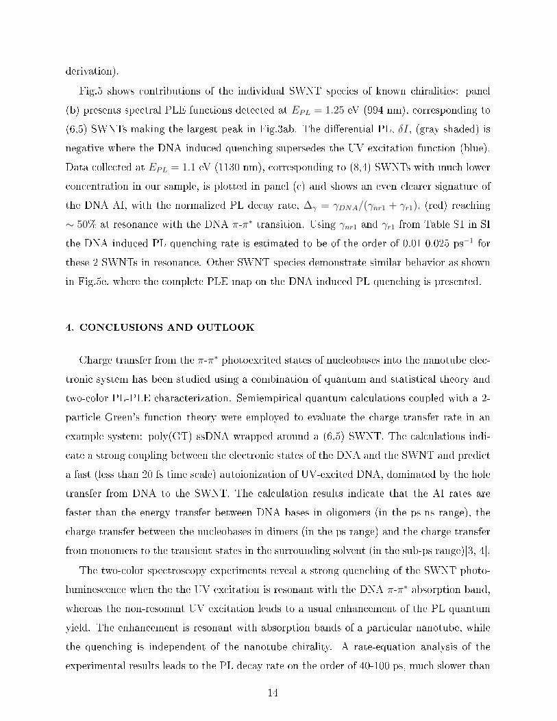
Fig.5 shows contributions of the individual SWNT species of known chiralities: panel
(b) presents spectral PLE functions detected at EPL = 1.25 eV (994 nm), corresponding to
(6,5) SWNTs making the largest peak in Fig.3ab. The di�erential PL, δI, (gray shaded) is
negative where the DNA induced quenching supersedes the UV excitation function (blue).
Data collected at EPL = 1.1 eV (1130 nm), corresponding to (8,4) SWNTs with much lower
concentration in our sample, is plotted in panel (c) and shows an even clearer signature of
the DNA AI, with the normalized PL decay rate, ∆γ = γDNA/(γnr1 + γr1), (red) reaching
∼ 50% at resonance with the DNA π-π∗ transition. Using γnr1 and γr1 from Table S1 in SI
the DNA induced PL quenching rate is estimated to be of the order of 0.01-0.025 ps−1 for
these 2 SWNTs in resonance. Other SWNT species demonstrate similar behavior as shown
in Fig.5e, where the complete PLE map on the DNA induced PL quenching is presented.
4. CONCLUSIONS AND OUTLOOK
Charge transfer from the π-π∗ photoexcited states of nucleobases into the nanotube elec-
tronic system has been studied using a combination of quantum and statistical theory and
two-color PL-PLE characterization. Semiempirical quantum calculations coupled with a 2-
particle Green's function theory were employed to evaluate the charge transfer rate in an
example system: poly(GT) ssDNA wrapped around a (6,5) SWNT. The calculations indi-
cate a strong coupling between the electronic states of the DNA and the SWNT and predict
a fast (less than 20 fs time scale) autoionization of UV-excited DNA, dominated by the hole
transfer from DNA to the SWNT. The calculation results indicate that the AI rates are
faster than the energy transfer between DNA bases in oligomers (in the ps-ns range), the
charge transfer between the nucleobases in dimers (in the ps range) and the charge transfer
from monomers to the transient states in the surrounding solvent (in the sub-ps range)[3, 4].
The two-color spectroscopy experiments reveal a strong quenching of the SWNT photo-
luminescence when the the UV excitation is resonant with the DNA π-π∗ absorption band,
whereas the non-resonant UV excitation leads to a usual enhancement of the PL quantum
yield. The enhancement is resonant with absorption bands of a particular nanotube, while
the quenching is independent of the nanotube chirality. A rate-equation analysis of the
experimental results leads to the PL decay rate on the order of 40-100 ps, much slower than
14

the calculated autoionization rate. This suggests that thermalization of the hot carriers
transferred from the DNA is the bottleneck of the autoionization-induced PL quenching.
We propose that two-color (and, potentially, multi-color) pump-probe experiments, simi-
lar to the one presented here, could become a useful technique for detecting charge transfer
in various molecular complexes. In the case of DNA, decoupling of DNA excitation fre-
quency (UV) from the sensor and pump frequencies (NIR and visible) enables spectroscopic
studies of DNA ionization under a range of experimental conditions. For example, one could
employ the method for studying autoionization in self-assembled DNA-SWNT complexes,
stable at ambient conditions in water solution and capable of penetrating live cells[12]. Our
calculations indicate that DNA-to-SWNT AI is a dominant process that makes SWNTs ideal
reporters in which the problems of previous sensor systems, for example, due to intra-DNA
and DNA-to-solvent charge transport, have been minimized. Thus, changes in the DNA
charged state could be monitored at room temperature in water solution, eliminating the
need for cryogenic or vapor-phase measurements.
Further developments of the method involve studies of SWNTs of di�erent chirality
wrapped with di�erent DNA. A combination of modeling and experimental studies sim-
ilar to ours, could presumably determine the sequence e�ect on the DNA autoionization
rates and identify the SWNT chirality best suited for AI monitoring from various DNA
sequences. Such a study could reveal the sequence-dependent AI processes that nature
presumably exploits to minimize the UV damage of DNA.
TI and SVR acknowledge support by National Science Foundation (ECCS-1202398 and
ECCS-1509786). AB acknowledges the startup fund support from the University of Central
Florida. The authors gratefully acknowledge access to facilities at the National Institute
of Standards and Technology for PL measurements and the computational time support
from the UCF Advanced Research Computing Center STOKES. We are thankful to Dr.
J. Fagan as the host at NIST, Dr. J. Reimers for providing us with the CNDO code, and
Dr. D. Roxbury for providing the MD trajectory.
Electronic Supplementary Material: Supplementary material contains details on the
sample preparation and experimental methods, and DNA autoionization modeling; dis-
cussion of the alternative recombination mechanisms; details on the rate equations and
PL quenching rate for DNA-induced non-radiative recombination channel; the experimen-
tally measured excitation functions for UV-vis pump, and the transmission data for UVLP
15

�lter; the rate equation parameters; the comparison of the DNA induced PL quenching
for 6 di�erent SWNT chiralities. ESM is available in the online version of this article at
http://dx.doi.org/10.1007/***********************
[1] C. T. Middleton, K. de La Harpe, C. Su, Y. K. Law, C. E. Crespo-Hernandez, and
B. Kohler, Annual Review of Physical Chemistry 60, 217 (2009), pMID: 19012538,
http://dx.doi.org/10.1146/annurev.physchem.59.032607.093719.
[2] A. Adhikary, A. Y. S. Malkhasian, S. Collins, J. Koppen, D. Becker,
and M. D. Sevilla, Nucleic Acids Research 33, 5553 (2005),
http://nar.oxfordjournals.org/content/33/17/5553.full.pdf+html.
[3] C. E. Crespo-Hernandez, B. Cohen, P. M. Hare, and B. Kohler, Chemical Reviews 104, 1977
(2004), pMID: 15080719, http://dx.doi.org/10.1021/cr0206770.
[4] Y. Zhang, J. Dood, A. A. Beckstead, X.-B. Li, K. V. Nguyen, C. J. Burrows, R. Improta,
and B. Kohler, The Journal of Physical Chemistry B 119, 7491 (2015), pMID: 25660103,
http://dx.doi.org/10.1021/jp511220x.
[5] N. K. Schwalb and F. Temps, Journal of the American Chemical Society 129, 9272 (2007),
pMID: 17622153, http://dx.doi.org/10.1021/ja073448+.
[6] C. E. Crespo-Hernandez and R. Arce, Photochemistry and Photobiology 76, 259 (2002).
[7] L. Belau, K. R. Wilson, S. R. Leone, and M. Ahmed, The Journal of Physical Chemistry A
111, 7562 (2007), pMID: 17419600.
[8] J. Gu, J. Leszczynski, and H. F. Schaefer, Chemical Reviews 112, 5603 (2012), pMID:
22694487, http://dx.doi.org/10.1021/cr3000219.
[9] J.-M. L. Pecourt, J. Peon, and B. Kohler, Journal of the American Chemical Society 122,
9348 (2000), http://dx.doi.org/10.1021/ja0021520.
[10] C.-R. Wang, T. Luo, and Q.-B. Lu, Phys. Chem. Chem. Phys. 10, 4463 (2008).
[11] M. Smyth and J. Kohano�, Phys. Rev. Lett. 106, 238108 (2011).
[12] G. Hong, S. Diao, A. L. Antaris, and H. Dai, Chemical Re-
views ASAP (2015), 10.1021/acs.chemrev.5b00008, pMID: 25997028,
http://dx.doi.org/10.1021/acs.chemrev.5b00008.
16

[13] Z. Liu, S. Tabakman, K. Welsher, and H. Dai, Nano Research 2, 85 (2009).
[14] E. Heister, E. W. Brunner, G. R. Dieckmann, I. Jurewicz, and A. B. Dalton, ACS Applied
Materials & Interfaces 5, 1870 (2013), pMID: 23427832, http://dx.doi.org/10.1021/am302902d.
[15] Z. Liu, J. T. Robinson, S. M. Tabakman, K. Yang, and H. Dai, Materials Today 14, 316
(2011).
[16] J. W. Kang, F. T. Nguyen, N. Lue, R. R. Dasari, and D. A. Heller, Nano Letters 12, 6170
(2012), pMID: 23151070, http://dx.doi.org/10.1021/nl302991y.
[17] J. L. Chilek, R. Wang, R. K. Draper, and P. Pantano, Analytical Chemistry 86, 2882 (2014),
pMID: 24564772, http://dx.doi.org/10.1021/ac403827m.
[18] A. Jain, A. Homayoun, C. W. Bannister, and K. Yum, Biotechnology Journal 10, 447 (2015).
[19] Y. Choi, I. S. Moody, P. C. Sims, S. R. Hunt, B. L. Corso, I. Perez, G. A. Weiss, and P. G.
Collins, Science 335, 319 (2012), http://www.sciencemag.org/content/335/6066/319.full.pdf.
[20] C. R. Martin and P. Kohli, Nat Rev Drug Discov 2, 29 (2003).
[21] W. Zhou, Y. Y. Wang, T.-S. Lim, T. Pham, D. Jain, and P. J. Burke, Sci. Rep. 5, (2015).
[22] J. Budhathoki-Uprety, P. V. Jena, D. Roxbury, and D. A. Heller, Journal of the American
Chemical Society 136, 15545 (2014), pMID: 25343218, http://dx.doi.org/10.1021/ja505529n.
[23] M. Zheng, A. Jagota, E. D. Semke, B. A. Diner, R. S. Mclean, S. R. Lustig, R. E. Richardson,
and N. G. Tassi, Nat Mater 2, 338 (2003).
[24] M. S. Strano, M. Zheng, A. Jagota, G. B. Onoa, D. A. Heller, P. W. Barone, and M. L. Usrey,
Nano Letters 4, 543 (2004), http://dx.doi.org/10.1021/nl034937k.
[25] G. Lu, P. Maragakis, and E. Kaxiras, Nano Letters 5, 897 (2005), pMID: 15884890,
http://dx.doi.org/10.1021/nl050354u.
[26] D. A. Heller, E. S. Jeng, T.-K. Yeung, B. M. Martinez, A. E. Moll, J. B. Gastala, and M. S.
Strano, Science 311, 508 (2006), http://www.sciencemag.org/content/311/5760/508.full.pdf.
[27] X. Tu, S. Manohar, A. Jagota, and M. Zheng, Nature 460, 250 (2009).
[28] C. Y. Khripin, S. Manohar, M. Zheng, and A. Jagota, The Journal of Physical Chemistry C
113, 13616 (2009), http://pubs.acs.org/doi/pdf/10.1021/jp903197d.
[29] S. V. Rotkin, Annual Review of Physical Chemistry 61, 241 (2010), pMID: 19947884,
http://dx.doi.org/10.1146/annurev.physchem.012809.103304.
[30] D. Roxbury, J. Mittal, and A. Jagota, Nano Letters 12, 1464 (2012).
[31] P. Cherukuri, S. M. Bachilo, S. H. Litovsky, and R. B. Weisman, Journal of the American
17

Chemical Society 126, 15638 (2004), pMID: 15571374, http://dx.doi.org/10.1021/ja0466311.
[32] B. Mu, J. Zhang, T. P. McNicholas, N. F. Reuel, S. Kruss, and M. S. Strano, Accounts of
Chemical Research 47, 979 (2014), pMID: 24467652, http://dx.doi.org/10.1021/ar400162w.
[33] A. Fabbro, S. Bosi, L. Ballerini, and M. Prato, ACS Chemical Neuroscience 3, 611 (2012),
http://dx.doi.org/10.1021/cn300048q.
[34] M. Calvaresi and F. Zerbetto, Accounts of Chemical Research 46, 2454 (2013), pMID:
23826731, http://dx.doi.org/10.1021/ar300347d.
[35] R. V. Mundra, X. Wu, J. Sauer, J. S. Dordick, and R. S. Kane, Current Opinion in Biotech-
nology 28, 25 (2014), nanobiotechnology and Systems biology.
[36] M. Zheng, A. Jagota, M. S. Strano, A. P. Santos, P. Barone, S. G. Chou, B. A. Diner, M. S.
Dresselhaus, R. S. Mclean, G. B. Onoa, G. G. Samsonidze, E. D. Semke, M. Usrey, and D. J.
Walls, Science 302, 1545 (2003), http://www.sciencemag.org/content/302/5650/1545.full.pdf.
[37] S. R. Lustig, A. Jagota, C. Khripin, and M. Zheng, The Journal of Physical Chemistry B
109, 2559 (2005), pMID: 16851257, http://dx.doi.org/10.1021/jp0452913.
[38] S. E. Snyder and S. V. Rotkin, JETP Letters 84, 348 (2006).
[39] S. Alidori, K. Asqiriba, P. Londero, M. Bergkvist, M. Leona, D. A. Scheinberg,
and M. R. McDevitt, The Journal of Physical Chemistry C 117, 5982 (2013),
http://dx.doi.org/10.1021/jp312416d.
[40] D. Roxbury, A. Jagota, and J. Mittal, The Journal of Physical Chemistry B 117, 132 (2013),
pMID: 23199189, http://dx.doi.org/10.1021/jp309523a.
[41] M. P. Landry, L. Vukovic, S. Kruss, G. Bisker, A. M. Landry, S. Islam, R. Jain,
K. Schulten, and M. S. Strano, The Journal of Physical Chemistry C 119, 10048 (2015),
http://dx.doi.org/10.1021/jp511448e.
[42] V. I. Puller and S. V. Rotkin, EPL (Europhysics Letters) 77, 27006 (2007).
[43] A. Wall and M. S. Ferreira, Journal of Physics: Condensed Matter 19, 406227 (2007).
[44] S. E. Snyder and S. V. Rotkin, Small 4, 1284 (2008).
[45] M. E. Hughes, E. Brandin, and J. A. Golovchenko, Nano Letters 7, 1191 (2007), pMID:
17419658, http://dx.doi.org/10.1021/nl062906u.
[46] H. Cathcart, V. Nicolosi, J. M. Hughes, W. J. Blau, J. M. Kelly, S. J. Quinn, and J. N.
Coleman, Journal of the American Chemical Society 130, 12734 (2008), pMID: 18761456,
http://dx.doi.org/10.1021/ja803273s.
18

[47] J. G. Duque, M. Pasquali, L. Cognet, and B. Lounis, ACS Nano 3, 2153 (2009).
[48] J. A. Fagan, M. Zheng, V. Rastogi, J. R. Simpson, C. Y. Khripin, C. A. Silvera Batista, and
A. R. Hight Walker, ACS Nano 7, 3373 (2013).
[49] E. J. Petersen, X. Tu, M. Dizdaroglu, M. Zheng, and B. C. Nelson, Small 9, 205 (2013).
[50] Y. Zhang, C. Liu, A. Balae�, S. S. Skourtis, and D. N. Beratan, Proceedings of the National
Academy of Sciences 111, 10049 (2014).
[51] B. Giese, J. Amaudrut, A. K. Kohler, M. Spormann, and S. Wessely, Nature 412, 318 (2001).
[52] R. N. Barnett, C. L. Cleveland, A. Joy, U. Landman, and G. B. Schuster, Science 294, 567
(2001).
[53] K. Senthilkumar, F. C. Grozema, C. F. Guerra, F. M. Bickelhaupt, F. D. Lewis, Y. A. Berlin,
M. A. Ratner, and L. D. A. Siebbeles, Journal of the American Chemical Society 127, 14894
(2005), doi: 10.1021/ja054257e.
[54] F. D. Lewis, T. F. Wu, Y. F. Zhang, R. L. Letsinger, S. R. Green�eld, and M. R. Wasielewski,
Science 277, 673 (1997).
[55] J. C. Genereux and J. K. Barton, Chemical Reviews 110, 1642 (2010).
[56] F. D. Lewis, H. H. Zhu, P. Daublain, T. Fiebig, M. Raytchev, Q. Wang, and V. Sha�rovich,
Journal of the American Chemical Society 128, 791 (2006).
[57] N. Renaud, Y. A. Berlin, F. D. Lewis, and M. A. Ratner, Journal of the American Chemical
Society 135, 3953 (2013).
[58] M. S. Dresselhaus, G. Dresselhaus, and P. Avouris, eds., Carbon Nanotubes: Synthesis, Struc-
ture, Properties and Applications, Vol. 80 in Springer Topics in Applied Physics (Springer
Verlag GmbH & Co. KG., 2001).
[59] H. Ajiki and T. Ando, J. Phys. Soc. Japan 62, 1255 (1993).
[60] T. Ignatova, H. Najafov, A. Ryasnyanskiy, I. Biaggio, M. Zheng, and S. V. Rotkin, ACS Nano,
ACS Nano 5, 6052 (2011).
[61] H. Jin, D. A. Heller, and M. S. Strano, Nano Letters 8, 1577 (2008), pMID: 18491944,
http://dx.doi.org/10.1021/nl072969s.
[62] T. Hertel, S. Himmelein, T. Ackermann, D. Stich, and J. Crochet, ACS Nano 4, 7161 (2010),
pMID: 21105744, http://dx.doi.org/10.1021/nn101612b.
[63] J. Ridley and M. Zerner, Theoretica chimica acta 32, 111 (1973).
[64] A. A. Voityuk, Wiley Interdisciplinary Reviews: Computational Molecular Science 3, 515
19
(2013).
[65] B. Tejerina and J. Reimers, �Cndo/indo,� (2008).
[66] R. Venkatramani, S. Keinan, A. Balae�, and D. N. Beratan, Coordination Chemistry Reviews
255, 635 (2011).
[67] R. Venkatramani, K. L. Davis, E. Wierzbinski, S. Bezer, A. Balae�, S. Keinan, A. Paul,
L. Kocsis, D. N. Beratan, C. Achim, and D. H. Waldeck, Journal of the American Chemical
Society 133, 62 (2011), times Cited: 18.
[68] E. Hatcher, A. Balae�, S. Keinan, R. Venkatramani, and D. N. Beratan, Journal of the
American Chemical Society 130, 11752 (2008).
[69] A. Fonseca, E. A. Perpete, P. Galet, B. Champagne, J. B. Nagy, J. M. Andre, P. Lambin, and
A. A. Lucas, Journal of Physics B: Atomic, Molecular and Optical Physics 29, 4915 (1996).
[70] A. A. Voityuk, Chemical Physics Letters 439, 162 (2007).
[71] A. A. Voityuk, The Journal of Chemical Physics 128, 115101 (2008).
[72] W. Thiel, Wiley Interdisciplinary Reviews: Computational Molecular Science 4, 145 (2014).
[73] A. A. Voityuk, Chemical Physics Letters 427, 177 (2006).
[74] S. Kilina and S. Tretiak, Advanced Functional Materials 17, 3405 (2007).
[75] H. Chen, M. A. Ratner, and G. C. Schatz, The Journal of Physical Chemistry C 115, 18810
(2011), http://dx.doi.org/10.1021/jp205262u.
[76] F. Santoro, R. Improta, F. Avila, M. Segado, and A. Lami, Photochem. Photobiol. Sci. 12,
1527 (2013).
[77] A. V. Tataurov, Y. You, and R. Owczarzy, Biophysical Chemistry 133, 66 (2008).
20

-3 -2 -1 0 1 2Energy, eV
DO
S,
a.u.
0
1
2
3
4
SWNTssDNA
0.01
MO
num
ber
AI time, fs
-1AI rate, fs
20
60
80
40
40
20
HOMOLUMO
0.03 0.300.09
90. 35. 4.010.55. 7.018.100
25
0
50
75
b
a
FIG. 1. (a) CNDO partial density of states (DOS) of the DNA (gray) and SWNT (pink) near
the charge neutrality point, calculated for one unit cell of a (6,5) nanotube wrapped with two
intertwined strands of poly(GT) DNA (red and blue in the inset). The DOS was calculated using
an empirical line broadening of 30 meV and a gap rescaling factor of 1.67. (b) Statistical distribution
of the AI rates for an electron excited in the 50 lowest unoccupied MOs (LUMO) and for a hole
in the 90 highest occupied MOs (HOMO). Note the scales of the upper and the lower axes are the
reciprocals of each other.
21

4.5 5.0 5.5
DNA absorption
Energy (eV)
E , E33 44E22E11
M
2
Abs
(arb
.uni
ts)
1.0 1.5 2.0 2.5 3.0 3.5 4.0 4.5 5.0
Photon energy (eV)
1
3 a
Inte
nsity
(arb
.uni
ts)
0
1000
750
500
250
PLE energy (eV)4.44.0 5.24.8
2.4 2.62.0 2.2
PL difference
(GT) Abs20
NT PLEUV
b
FIG. 2. (a) Absorption spectrum of DNA-SWNT solution. The SWNT absorption subbands are
labeled by Enn. The green and purple arrows indicate the two-color PL excitation range. The inset
shows the absorption spectrum of (GT)20 ssDNA[77]. (b) The UV part of the PLE spectrum of the
nanotube solution (purple solid symbols) taken at PL photon energy E = 1.11 eV (indicated by the
orange arrow in the top panel and Fig.3b), overlaid with the DNA absorption from the top panel
(green open symbols) and δI (gray line), measured at half of the photon energy (note the di�erent
scale of the top axis).
22

1.0 1.1 1.2 1.3
3000
6000
9000
1.0 1.1 1.2 1.3
d
caE xc itation:
λ =640nm
λ =640nm+320nm
λ =320nm
E xc itation:
λ =712nm
λ =712nm+356nm
λ =356nm
E xc itation:
λ =524nm
λ =524nm+262nm
λ =262nm
E xc itation:
λ =492nm
λ =492nm+246nm
λ =250nm
P L E nergy (eV )
PL
In
ten
sit
y
(arb
.un
its
)
b x2
0
FIG. 3. Single- and two-color PL spectra of DNA-SWNT solution. Legend shows excitation wave-
lengths: each panel presents PL emission induced by 1-color visible excitation (thick black line),
1-color UV (thin blue line), and 2-color combined UV and visible excitation (open symbols), taken
at PLE energies indicated by the same color arrows in Fig.2. Orange arrow indicates PL energy
where the UV PLE data was taken in Fig.2.
23

excitation
492 nm 246 nm
524 nm 262 nm
640 nm 320 nm
712 nm 356 nm
PL
dif
fere
nce
(ar
b.u
n.)
-1200
-800
-400
0
400
-1000
-600
-200
200
0.9 1.0 1.1 1.2 1.3
2000
4000
6000
8000
PL Energy (eV)
(10.5)
(8,6)
(7,6)
(9,4)
(7,5)
(6,5)(8,3)
(9,1)
PL
Inte
nsi
ty (
arb
.un
.)1C
524 nm
0
b
a
FIG. 4. (a) PL di�erence (∆I) for the same two-color excitation lines as in Fig.3: 492/246 nm,
524/262 nm, 640/320 nm, 712/356 nm (brown, red, gray, green). Negative di�erential PL at
additional UV-excitation in the band around 4.6 eV (265 nm) is observed, corresponding to the
DNA absorption band (Fig.2). (b) PL spectrum with one-color excitation at 2.36 eV (524 nm),
showing the same spectral features as the di�erential PL in top panel; each line is identi�ed with
an individual SWNT chirality.
24

PLE energy (eV)4.5 5.03.0 4.02.52.0 3.5
PL e
nerg
y (e
V)
1.0
1.1
1.2
1.3
Inte
nsity
(arb
.uni
ts)
Photon energy (eV)
0.0
2.4 2.62.0 2.21.8-0.2
0.8
0.6
0.4
0.2M/(M+1)
(8,4)
- δ Ι
∆γ∆γ∆γ
(6,5)
AI t
ime
(fs)
UV Photon energy (eV)4.8 5.24.0 4.4
150
100
50
25
0
75
125
Inte
nsity
(arb
.uni
ts)
Photon energy (eV)
0.0
2.4 2.62.0 2.21.8-0.2
0.8
0.6
0.4
0.2M/(M+1)
∆γ∆γ∆γ
- δ Ι
(6,5)
- δ Ι
(6,5)
(8,4)
Phot
on e
nerg
y (e
V)
Photon energy (eV)2.4 2.62.0 2.21.8
1.0
1.1
1.2
1.3 4.8 5.24.0 4.4
Guv
π−π*τ1r
τ2nr
τ1nr
Gvis
τ32
τ21
AIDNA
τDNA
Guvτ1r
τ2nr
τ1nr
Gvis
τ32
τ21
Guv
a b c
d e f
FIG. 5. (a) Sketch of electronic transitions after (right) resonant UV excitation of DNA, followed
by AI of the π-π∗ excited state (red lines); (left) o�-resonance excitation, not followed by AI. Blue
curves show UV-excitation and corresponding transition rates; green/gray curves correspond to
visible/NIR range (see text for details). (b-c) Spectral decay function ∆γ (red), di�erential PL
function −δI (gray), and excitation ratio function M(M + 1) (blue) for (b) the (6,5) SWNT, PL
peak at 1.25 eV, bottom red line in panel (e); and (c) the (8,4) SWNT, PL peak at 1.1 eV, top red
line in panel (e). (d) DNA-SWNT PL/PLE map at 1-color excitation. (e) Di�erential PL/PLE map
of the same sample as in (d). Cross-sections of −δI map at the positions of red lines, corresponding
to (8,4) and (6.5) SWNTs, are shown in panels (b-c). Horizontal axis shows double scale: PLE
visible range excitation (black) same as in panel (b) above it, and UV pump (purple) same as in
panel (f). (f) Dynamics of autoionization spectra of the π-π∗ excited state of DNA-SWNT complex:
the AI probability of (6,5) SWNT wrapped with (GT)-sequence vs. photon energy of UV pump
(horizontal axis) and time (vertical). Note the PLE UV photon energy is double the one in the
panel (c) above it.
25

Two-color spectroscopy of UV excited ssDNA complex with a
single-wall nanotube photoluminescence probe: Fast relaxation by
nucleobase autoionization mechanism
Tetyana Ignatova and Michael Blades
Physics Department, Lehigh University,
16 Memorial Dr. E., Bethlehem, PA 18015
Alexander Balae�
NanoScience Technology Center, University of Central Florida,
12424 Research Parkway, Suite 400, Orlando, FL 32826
Ming Zheng
National Institute of Standards and Technology,
100 Bureau Drive, Gaithersburg, MD 20899
Peter Stoeckl
Department of Physics & Astronomy, University of Rochester,
206 Bausch & Lomb Hall, Rochester, NY 14627
Slava V. Rotkin
Physics Department, Center for Advanced Materials &
Nanotechnology and Center for Photonics & Nanoelectronics,
Lehigh University, 16 Memorial Dr. E., Bethlehem, PA 18015
1

SUPPLEMENTARY INFORMATION: TABLE OF CONTENT
1. Details on DNA autoionization modeling
2. Discussion of alternative recombination mechanisms
3. Rate equations and PL quenching rate for DNA-induced non-radiative recombination
channel
4. Experimentally measured excitation functions for UV-vis pump
5. Transmission data for UVLP �lter
6. Rate equation parameters
7. Comparison of the DNA induced PL quenching for 6 di�erent SWNT chiralities
2

SI: DETAILS ON DNA AUTOIONIZATION MODELING
Although modeling of a DNA-SWNT-water system of the same size as in the experiment
is beyond our current computing abilities, we were able to provide clear theoretical evidence
for fast AI of the π-π∗ excited states in DNA wrapped around a typical SWNT.
The most abundant SWNT species in the CoMoCat samples are known to be (6,5) nan-
otubes (see Fig.2). The MD simulation was done on a fragment of (6,5) SWNT with two
intertwinned ssDNA oligomers (GT)n where n = 30, as shown in Fig.1 (upper inset). Al-
though ssDNA with n = 20 has been used in our experiments, we note that both olygomers
have been shown earlier to make a similar wrapping on the nanotube surface[1]. Frames
taken after several ns of MD simulation were used to determine the geometry of the DNA-
SWNT complex solvated in TIP3P water box. A shorter chain with 14-20 bases (excluding
backbone) along with the single unit cell of (6,5) SWNT (364 atoms) were used for quan-
tum modeling due to computational expenses. The quantum-chemistry INDO/s calculation
has been performed, followed by a Green's Function based calculation of the autoionization
within a perturbation theory. Time-dependent AI probability for a π-π∗ excited DNA base
was calculated (for various con�gurations) and analyzed (see main text for statistics of AI
collected over the whole trajectory). The AI probability was also convolved with the theo-
retical excitation spectrum, giving the total e�ciency of UV-ionization, as measured in the
experiment.
Here we provide more details on the quantum-mechanical model. Let us denote by |b〉
the Dirac states of DNA only, taken in a water environment, which are solutions of the
corresponding Hamiltonian Hb:
Hb|b〉 = Eb|b〉 (1)
where the quantum number b labels non-hybridized (bare) MOs (the energy of the states
was renormalized in order to match the experimental absorption band). These Dirac states
are mostly localized on individual bases.
Corresponding states of the isolated SWNT are derived from a similar equation:
Hq|q〉 = Eq|q〉 (2)
where the quantum number q includes both linear and angular momentum, as well as all
other required quantum numbers for the SWNT one-electron energy levels. Those levels
3

are degenerate due to the high symmetry of the SWNT, except for a few MOs of special
symmetry. The Green's function of the combined system will be de�ned via the total
Hamiltonian:
H|n〉 = (Hb +Hq + V )|n〉 = En|n〉 (3)
where V is the interaction/coupling between the DNA and the SWNT, n labels the complete
set of hybridized MOs of the complex. We will use below a special notation to distinguish
unoccupied orbitals: |n�〉.
This formalism allows us to de�ne the electron autoionization process as an evolution of
the π-π∗ excited state into the state with the electron on the SWNT and the "hole" on the
DNA (or vice versa). The initial (many-particle) Dirac state is given by: |bb�, 0〉, where we
denote the SWNT ground state by zero. The �nal state is 〈b′, qc| (correspondingly for hole
tunneling we take 〈b�, qv| as the �nal state). We stress that in both initial and �nal state
b, b′ MOs correspond to the vacant state among normally occupied orbitals (a hole). Two
other states: b� and qc belong to normally occupied (particle) states. The scattering Green's
function is as follows (notice that ~ = 1 in this section):
Gb′qc,bb�(t) = 〈b′, qc|e−iHt|bb�, 0〉 =∑
nn�,mm�
〈b′, qc|nn�〉〈nn�|e−iHt|mm�〉〈mm�|bb�, 0〉 (4)
where in the r.h.s. we use spectral decomposition over the complete particle-hole basis set.
We allow the �nal state to have a hole in a di�erent MO b′ 6= b (which corresponds to the
hole which tunnels to another base along the DNA chain). Similarly we can write a Green
function for the process of an autoionization of the hole into the SWNT when the electron
stays at the DNA in the �nal state:
G[h]
b�′qv ,bb�(t) = 〈b�′, qv|e−iHt|bb�, 0〉 =
∑nn�,mm�
〈b�′, qv|nn�〉〈nn�|e−iHt|mm�〉〈mm�|bb�, 0〉 (5)
Neglecting small overlap integrals between occupied and unoccupied states 〈m|b�〉, 〈b|m�〉 →
0, which has been con�rmed numerically, and assuming the thermal equilibrium concentra-
tions of electrons in unoccupied orbitals: N(n�)e = 〈a†n�an�〉 and holes in the occupied orbitals:
N(n)h = 〈ana†n〉 are negligible compared to unity, the Green's function Eq.(4) may be written
as:
Gb′qc,bb�(t) =∑nn�
〈qc|n�〉〈n|b′〉〈b|n〉〈n�|b�〉e−i(En�−En)t = Gqcb�(t)Gbb′(−t) (6)
4

and it separates into two one-particle Green functions for the electron and hole components:
Gqcb�(t) =∑n�
〈qc|n�〉〈n�|b�〉e−iEn� t Gbb′(−t) =∑n
〈b|n〉〈n|b′〉e+iEnt = G+b′b(t) (7)
The probability of autoionization is:
P = G(t)G+(t) = Pe + Ph = Gb′qc,bb�(t)Gbb�,b′qc(−t) + [holes] (8)
= Gqcb�(t)Gb�qc(−t)Gbb′(−t)Gb′b(t) + [holes]
Fig.1 shows the representative time dynamics of the hole AI for several HOMOs, as labeled
in the �gure legend. Rabi oscillations are prominent, overlaid with an overall increase of the
probability to �nd a hole with its �nal state on the SWNT (anywhere in the valence band).
The middle panel shows statistics for a G- and T-base population of the 40 MOs with the
smallest energy (counted from the charge neutrality point).
FIG. 1. (top inset) Geometry of the whole system. (middle) Statistics of G- and T-base distribution
of the smallest energy MOs (20 HOMOs and 20 LUMOs). (bottom) Probability of AI (by hole) for
9 highest occupied MOs for one representative frame of MD.
5
SI: DISCUSSION OF ALTERNATIVE RECOMBINATION MECHANISMS
The quantum yield of PL is proportional to the ratio: γr1γnr1+γr1
' γr1γnr1
, which decreases
under second-color UV illumination. Thus, the non-radiative rate in the lowest exciton
state should increase or the radiative rate should decrease. According to a detailed equi-
librium principle, the latter should be accompanied with lower absorption (bleaching). UV
irradiation was previously suggested to have a direct in�uence on the nanotube electronic
structure, for example, via UV-assisted defect creation, SWNT functionalization or for-
mation of chemical bonds [2, 3] that lead to lower γr1. This resulted in absorption and
PL bleaching, typically long lasting e�ects with appreciable recovery times which were not
observed in our case. This is likely because our samples contain tubes densely wrapped
with the (GT) DNA, which is known to cover the SWNT surface densely[4] without holes,
suppressing surface functionalization [5].
In this work we introduce a new nonradiative mechanism of exciton decay. Here we brie�y
discuss several existing mechanisms and argue why they cannot explain our two-color PL.
Three main groups of PL nonradiative decay channels were considered in the earlier works:
1. At very high excitation intensity, when the number of excitons per SWNT is larger
(much larger) than one, the exciton-exciton (Auger recombination) decay mechanism [6] is
important. A similar exciton-electron Auger recombination was shown to be less e�cient
[7, 8] than the multi-exciton channel due to strong restrictions imposed on the symmetry of
electronic states participating in such a transition. These symmetry conditions are di�cult
to satisfy in a two-particle process, unless there are bound electrons in deep (mid-band-gap),
strongly localized states or numerous free charge carriers in conduction or valence bands.
2. For an exciton (or e-h pair) in the E22 (and higher) subbands which overlaps with the
single-electron continuum in a lower subband (for example, E11), the electron-electron [9] (or
electron-phonon [10]) scattering results in an intersubband relaxation. This non-radiative
channel naturally does not apply to E11 excitons, lying below a corresponding single-electron
continuum of states.
3. Many-particle (multi-state) non-radiative channels can become very e�cient under the
condition that (a) many-particle interaction satis�es required symmetry selection rules and
(b) the process is resonant in energy, that is, the energy of the many-particle state coincides
with the exciton energy. Such mechanisms include PAIEI [7] and a number of defect- or
6

impurity-based exciton scattering models [10�14].
The mechanisms 2 and 3 were not shown to be activated by light.
Because of the protective DNA layer, densely coating the SWNT surface, defect formation
and non-radiative exciton recombination mechanisms based on it seem unlikely to happen
in our experiment. Even though the DNA wrapping could be, arguably, corrupted during
the UV irradiation, we did not detect this e�ect in our samples. This would allow access
of water molecules to the SWNT surface thus increasing the non-radiative decay. However,
it is inconsistent with the fact that the anomalous PL was fully reversible and recovered
instantaneously after the second-color illumination was turned o�. Also the solution con-
tained no free DNA, since pure heavy water was substituted for the DNA citric bu�er in
our samples. In the event of DNA desorption from the tube walls under UV irradiation, its
concentration in solution will be minuscule and the reverse process of restoration of the wrap
will not happen for entropy reasons. Thus the DNA unwrapping, if it happened, should be
easily detectable in our experiments. We note that we did not observe the e�ect in tubes
suspended with DOC or SDBS, where the concentration of the free surfactant in solution is
always high and surfactant molecules may indeed exchange between solvated phase and the
phase agglomerated on the tube surface [15, 16].
Excitation power was 6× 10⁻⁵ light quanta per tube, always below the limit of creating
multiple excitations per tube. Thus any exciton-exciton interaction mechanisms can be dis-
regarded under main (visible) excitation, and even more under the weaker UV illumination.
Finally, the intersubband relaxation mechanisms can be excluded, due to non-overlap of the
E11 exciton with its continuum. Then only mechanisms involving free charge carriers need
to be considered.
It is known that additional free charge carriers enhance nonradiative recombination rates
[17, 18]. However, direct generation of the e-h pairs in the upper SWNT subbands with the
UV pump shows a resonant enhancement at the PLE lines of these subbands and should
vary with the SWNT chirality (not consistent with the data). Besides this, the exciton
generation still leaves the total charge density of SWNT the same, and does not break
the charge neutrality by itself. Thus, it does not lead to tube doping and cannot explain
the decrease in the PL yield unless additional ionization and/or trapping mechanisms are
invoked.
Therefore, one has to assume that there is a new mechanism, providing a steady-state
7

doping of the SWNT, due to a resonant photoexcitation of the tube surrounding. The
photoexcited states should be shallow enough to allow fast "instantaneous" response upon
turning two-color excitation on and o�. This excludes the electrons trapped in solvated
states in surrounding water. We note that the same samples showed an interesting PL
behavior during the formation of the complexes with the multivalent ions[19] to be discussed
elsewhere.
What could be the origin of these shallow states? We show in the main text that the
resonantly photoexcited DNA undergoes a π-π∗ transition, with the energy of the excitation
above the forbidden gap of the DNA ∼ 4.2 eV, and then transfers the excited charge carrier
into the SWNT valence and conduction bands. Similar charge transfer has been observed
earlier in other SWNT hybrids: with porphyrines [20], fullerenes [21], and organic molecules
[22]. Indeed the DNA ionization potential is 8.9-9.3 eV and 8.25-8.62 eV [23, 24] for thymine
and guanine bases correspondingly, it can vary in di�erent solvation states. Thus the excited
π∗ states are in resonance with the conduction bands of a typical SWNT, which has a work
function on the order of 5 eV and a band gap or the order of 1 eV.
We show in the main text that the photoexcited DNA electron can autoionize in the
SWNT bands. This creates an additional free charge carrier density (although the whole
complex DNA-SWNT is electrically neutral), which facilitates the electron-electron scatter-
ing and non-radiative decay of the E11 exciton. Such a mechanism would not vary among
SWNTs of di�erent chirality unless the photoexcited state moves out of the resonant window,
thus decreasing the autoionization rate. This, however, would require tubes with extremely
large band gaps, not found in our samples.
SI: RATE EQUATIONS AND PL QUENCHING RATE FOR DNA-INDUCED NON-
RADIATIVE RECOMBINATION CHANNEL
We use rate equations for a 4-level system of exciton manifolds (including the ground
state) of the SWNT. Here Eii where i = 1, 2, 3 is the subband index of the lowest exciton
8

subbands, coupled to each other and to the ground state via the classical rate equations:
dn1
dt= −γr1n1 − γnr1n1 − γDNAn1 + γ21n2
dn2
dt= −γr2n2 − γnr2n2 − γ21n2 + γ32n3 +Gvis
dn3
dt= −γr3n3 − γnr3n3 − γ32n3 + ηGuv,
(9)
where ni is the exciton population of the ith level (the Eii state), Gvis, Guv are generating
functions (excitation/pump spectral functions), η is the second-color excitation e�ciency,
γij are intersubband relaxation rates, and γri/γnri are the radiative/nonradiative rates of
the corresponding states. Radiative and nonradiative rates were taken from [9, 10, 25]
and presented in Table I. Generating functions were directly measured with single-color
excitation and presented in Fig.2.
In addition to standard coupling parameters γij, γri, γnri, known from previous works
on monochromatic excitation, we add a new non-radiative decay rate: γDNA, speci�c to
the nonradiative recombination channel induced in the E11 subband by second-color pho-
toexcitation (UV). We assign this channel to the photoexcitation of the DNA followed by
autoionization in the E11 subband, as described in the main text.
The steady-state left hand side equals zero in Eq.(9), allowing a simple solution for the
populations of the states, ni, if the generation spectral functions Gvis,uv are known. In
neglecting the radiative transition from all levels except for the lowest one, the total PL
intensity is given by the product of the radiation rate of this level and it's population factor:
γr1n1. After simple math it can be written as a product of three terms:
Iuv+vis = γr1ni =
(Gvis + ηGuv
γ32γ32 + γr3 + γnr3
)
×(
γ21γ21 + γr2 + γnr2
)(γr1
γr1 + γnr1 + γDNA
) (10)
where the term R3 = γ32/(γ32 + γr3 + γnr3) accounts for the relaxation of the charge carriers
from the E33 subband into the E22 subband, the second term gives a similar internal yield
for the intersubband relaxation of E22 charge carriers into the E11 subband, and the last
term is the PL e�ciency in the lowest E11 subband. Here we explicitly included γDNA, an
additional non-radiative relaxation rate due to the photoexcited DNA. We assume that the
9
conversion rate in the upper subbands is large: R3 ≈ 1/2 or larger and that it is independent
of the excitation energy which is probably accurate due to the fast and e�cient intrasubband
relaxation. Then it can be included together with the UV e�ciency in a single factor ηuv,
and we rewrite the solution as:
Iuv+vis = Gvis
(γ21
γ21 + γr2 + γnr2
)(γr1
γr1 + γnr1
)
×(
1 + ηuvGuv
Gvis
) (γr1 + γnr1
γr1 + γnr1 + γDNA
) (11)
where the �rst three terms can be related to the PL intensity at the single-color (visible)
excitation. In order to compare this with the experimental data one needs to correct the
generation spectral function (pump) by the transmission through the UVLP �lter. We had
to measure this correction function ourselves due to a found inconsistency with the nominal
transmission data presented by the manufacturer (see Fig.3). Finally, the single-color PL
intensity (while blocking the UV-line with a �lter) can be written as:
Ivis = Gvis
(γ21
γ21 + γr2 + γnr2
)(γr1
γr1 + γnr1
)(12)
where Gvis = GvisTUV LP is the visible excitation spectral function corrected for UVLP �lter
transmission.
Two-color PL intensity is then:
Iuv+vis =Ivis
TUV LP
(1 +
ηuvGuv
Gvis
) (γr1 + γnr1
γr1 + γnr1 + γDNA
)(13)
We did not make any approximation in this expression yet, except for assuming ηuv to be
independent of energy (which includes an energy independent factor R3). It is useful to
resolve Eq.(13) for γDNA, for which the solution is given by:
γDNA = (γnr1 + γr1)
Ivis
TUV LP
(1 + ηuv
Guv
Gvis
)Ivis+uv
− 1
(14)
We emphasize that all quantities here are the experimentally measured ones: Ivis and Ivis+uv
are the PL intensity under one-color (vis) and two-color (vis+uv) excitation correspondingly;
TUV LP is the correction transmission function of the UVLP �lter; Guv and Gvis are the
excitation functions for one-color illumination; and ηuv is the constant UV pump e�ciency
∼ 10%.
10

Total excitation is given by:
Gtotal = Gvis + ηuvGuv = Gvis (1 +M). (15)
where we single out the excitation e�ciency ratio:
M = ηuvGuv
Gvis
(16)
which shows how strong the second-color pump is compared to the main color source. When
M� 0 the UV excitation creates a large number of excitons in higher subbands and gives a
considerable rise to the total PL. We also provide, for the sake of completeness, an expression
for the relative e�ciency of the dual-color excitation with respect to the single-color one:
M1 +M
= 1− G1C
G2C
(17)
In the main text we de�ned the di�erential PL function as:
∆I = Ivis+uv − Ivis = Ivis+uv − T−1UV LP Ivis. (18)
Corresponding normalized di�erential PL can be de�ned as the ratio:
δI =∆I
Ivis+uv=
(1− T−1UV LP I
vis
Ivis+uv
)(19)
In the main text we also de�ned the normalized spectral quenching rate:
∆γ =γDNA
γnr1 + γr1=
γDNAγtot1C − γDNA
(20)
where γnr1 is the non-radiative rate and γr1 is the radiative recombination rate in the E11
subband measured for one-color (vis) excitation. Then γnr1+γr1 and γtot1C = γDNA+γnr1+γr1
are the total decay rates under one-color and dual-color pumps respectively.
Substituting Eqs.(12,13) into (19) and making use of the short-cut notations given by
Eqs.(16,20) we obtain the following formula:
δI =1
1 +M(M−∆γ). (21)
We emphasize that all the terms are non-negative. The anomalous (negative) di�erential
PL corresponds toM≤ ∆γ.
Substituting Eqs.(12,13) into (20) and making use of the same short-cut notations, we
obtain the DNA decay rate as a percent of the one-color total decay rate, γnr1 + γr1:
γDNA = (γnr1 + γr1)
(T−1UV LP I
vis
Gvis
Gvis + ηuvGuv
Ivis+uv− 1
)(22)
11

which can be simpli�ed for data analysis by using short-cut notations for one/two-color PL
quantum yield:
QY1C =T−1UV LP I
vis
Gvis
QY2C =Ivis+uv
Gvis + ηuvGuv
(23)
which �nally results in Eq.(8)of the main text:
γDNA = (γnr1 + γr1)
(QY1CQY2C
− 1
). (24)
SI: EXPERIMENTALLY MEASURED EXCITATION FUNCTIONS FOR UV-VIS
PUMP
Experimentally measured excitation functions (generation term in the rate equations)
Gvis and Guv are presented in Fig.2. The data is combined from 3 separate measurements,
normalized by the total PL excitation strength, following the procedure from[26]. Eleven
SWNT species were found in the CoMocat solution: all of the strongest (n,m) peaks in the
visible range are indicated on the Figure.
250
PLE
(nm
)
PL (nm)
750
650
550
450
350
1050850 1150 1250 1350950
(6,4)(6,5)
(7,5)(9,5)
(9,1) (9,4)
(9,2)
(7,6)
(8,4)
(8,6)
(8,3)
FIG. 2. Complete excitation function in the range of PL excitation: 250-760 nm and PL range
850-1350 nm is shown.
SI: TRANSMISSION DATA FOR UVLP FILTER
Fig.3 shows the experimental (measured) absorption spectrum of the UVLP-450 �lter,
compared to the table data provided by the manufacturer[27]. A clear di�erence is seen
12

TABLE I. Rate equation parameters (all γ are in ps−1; ? for resonant absorption of DNA wrapped
on (6,5) SWNT).
γr1 γr2,3 γnr1 γnr2,3 γ21,32 γ?DNA
6.3×10⁻⁴ 10−3 0.035-0.05 6.3×10⁻³ 76.9 0.017-0.025
between nominal and actual data which should be taken into account in rate equation
analysis.
100Tr
ansm
issi
on
(%
)
Energy (eV)
80
40
60
20
1.81.6 2.62.42.0 2.2 2.8
FIG. 3. Real UVLP transmission data (red), compared to the nominal transmission, available
online (gray).
SI: RATE EQUATION PARAMETERS
All SWNT rates used in the rate equation analysis are given in TableI along with the
maximum rates calculated for the DNA induced PL quenching.
SI: COMPARISON OF THE DNA INDUCED PL QUENCHING FOR 6 DIFFERENT
SWNT CHIRALITIES
The normalized di�erential PL, δI, for a (6,5) nanotube is shown in Fig.4 along with the
excitation e�ciency functionM/(M+ 1) and the normalized function ∆γ. For a (6,5) tube
the DNA induced exciton quenching can reach above 30% of the total non-radiative decay
rate. Other chiralities show similar di�erential PLE spectra with two main features: on the
UV side each δI spectrum has a negative band (note that the abscissa axis is reversed for
δI) around 530 nm where the intensity of one-color (vis) excitation PL exceeds the two-
color PL intensity. This also corresponds to the region of low e�ciency of the UV pump
13

NT (6.5)
1.6 1.8 2.0 2.2 2.4 2.6
-0.2
0.0
0.2
0.4
0.6
0.8
Eexcvis , eV
M/(1+M),-δI,Δγ(arb.un.) NT (7.5)
1.6 1.8 2.0 2.2 2.4 2.6
-0.2
0.0
0.2
0.4
0.6
0.8
Eexcvis , eV
M/(1+M),-δI,Δγ(arb.un.)
NT (8.3)
1.6 1.8 2.0 2.2 2.4 2.6
-0.2
0.0
0.2
0.4
0.6
0.8
Eexcvis , eV
M/(1+M),-δI,Δγ(arb.un.) NT (7.6)
1.6 1.8 2.0 2.2 2.4 2.6
-0.2
0.0
0.2
0.4
0.6
0.8
Eexcvis , eV
M/(1+M),-δI,Δγ(arb.un.)
NT (9.2)
1.6 1.8 2.0 2.2 2.4 2.6
-0.2
0.0
0.2
0.4
0.6
0.8
Eexcvis , eV
M/(1+M),-δI,Δγ(arb.un.) NT (9.4)
1.6 1.8 2.0 2.2 2.4 2.6
-0.2
0.0
0.2
0.4
0.6
0.8
Eexcvis , eV
M/(1+M),-δI,Δγ(arb.un.)
NT (8.6)
1.6 1.8 2.0 2.2 2.4 2.6
-0.2
0.0
0.2
0.4
0.6
0.8
Eexcvis , eV
M/(1+M),-δI,Δγ(arb.un.) NT (9.5)
1.6 1.8 2.0 2.2 2.4 2.6
-0.2
0.0
0.2
0.4
0.6
0.8
Eexcvis , eV
M/(1+M),-δI,Δγ(arb.un.)
FIG. 4. The excitation function, M/(1 + M), (green), the PL di�erence, −δI, (black), and the
PL quenching function, ∆γ , (red). Graphics table compares the data for 8 SWNT species from 11
found in solution .
(M << 1). On the IR side (forM∼ 1) several features can be found. They are positioned
di�erently for di�erent tubes following the pattern of individual resonances of a particular
SWNT (compare di�erent chiralities in Fig.4). These features correspond to the resonant
UV excitation which increases the PL signal and compensates for the e�ect of the DNA
(M > ∆γ). The anomalous PL can be observed only for smallM, in the region where the
direct UV pump is insu�cient compared to the main excitation line.
14

[1] S. R. Lustig, A. Jagota, C. Khripin, and M. Zheng, The Journal of Physical Chemistry B
109, 2559 (2005), pMID: 16851257, http://dx.doi.org/10.1021/jp0452913.
[2] J. J. Crochet, S. Hoseinkhani, L. Luer, T. Hertel, S. K. Doorn, and G. Lanzani, Phys. Rev.
Lett. 107, 257402 (2011).
[3] M.-H. Ham, B.-S. Kong, W.-J. Kim, H.-T. Jung, and M. S. Strano, Phys. Rev. Lett. 102,
047402 (2009).
[4] We cannot exclude that UV irradiation may in�uence defects at the ends of the tubes which
are open to water, however such mechanism should be negligible due to the high aspect ratio
of our tubes (the length ∼ 400 nm).
[5] D. Roxbury, J. Mittal, and A. Jagota, Nano Letters 12, 1464 (2012).
[6] F. Wang, Y. Wu, M. S. Hybertsen, and T. F. Heinz, Phys. Rev. B 73, 245424 (2006).
[7] V. Perebeinos and P. Avouris, Phys. Rev. Lett. 101, 057401 (2008).
[8] Z. Zhu, J. Crochet, M. S. Arnold, M. C. Hersam, H. Ulbricht, D. Resasco, and T. Hertel, The
Journal of Physical Chemistry C 111, 3831 (2007).
[9] T. Hertel, S. Himmelein, T. Ackermann, D. Stich, and J. Crochet, ACS Nano 4, 7161 (2010),
pMID: 21105744, http://dx.doi.org/10.1021/nn101612b.
[10] D. M. Harrah, J. R. Schneck, A. A. Green, M. C. Hersam, L. D. Ziegler, and A. K. Swan,
ACS Nano 5, 9898 (2011).
[11] J. Lefebvre, P. Finnie, and Y. Homma, Phys. Rev. B 70, 045419 (2004).
[12] J. J. Crochet, J. G. Duque, J. H. Werner, and S. K. Doorn, Nat Nano 7, 126 (2012).
[13] D. M. Harrah and A. K. Swan, ACS Nano 5, 647 (2011),
http://pubs.acs.org/doi/pdf/10.1021/nn1031214.
[14] S. Ghosh, S. M. Bachilo, R. A. Simonette, K. M. Beckingham, and R. B. Weisman, Science
330, 1656 (2010).
[15] J. G. Duque, G. Gupta, L. Cognet, B. Lounis, S. K. Doorn, and A. M. Dattelbaum, The
Journal of Physical Chemistry C 115, 15147 (2011).
[16] D. Roxbury, X. Tu, M. Zheng, and A. Jagota, Langmuir 27, 8282 (2011).
[17] J. M. Kinder and E. J. Mele, Phys. Rev. B 78, 155429 (2008).
[18] K. Matsuda, Y. Miyauchi, T. Sakashita, and Y. Kanemitsu, Phys. Rev. B 81, 033409 (2010).
15

[19] T. Ignatova, M. Blades, J. G. Duque, S. K. Doorn, I. Biaggio, and S. V. Rotkin, Phys. Chem.
Chem. Phys. 16, 26715 (2014).
[20] J. P. Casey, S. M. Bachilo, and R. B. Weisman, J. Mater. Chem. 18, 1510 (2008).
[21] F. D'Souza, R. Chitta, A. S. D. Sandanayaka, N. K. Subbaiyan, L. D'Souza, Y. Araki, and
O. Ito, Journal of the American Chemical Society 129, 15865 (2007), pMID: 18052162.
[22] L. Hu, Y.-L. Zhao, K. Ryu, C. Zhou, J. Stoddart, and G. Gruner, Advanced Materials 20,
939 (2008).
[23] D. Roca-Sanjuan, M. Rubio, M. Merchan, and L. Serrano-Andras, The Journal of Chemical
Physics 125, 084302 (2006).
[24] L. Belau, K. R. Wilson, S. R. Leone, and M. Ahmed, The Journal of Physical Chemistry A
111, 7562 (2007), pMID: 17419600.
[25] F. Schoppler, C. Mann, T. C. Hain, F. M. Neubauer, G. Privitera, F. Bonaccorso, D. Chu,
A. C. Ferrari, and T. Hertel, The Journal of Physical Chemistry C 115, 14682 (2011).
[26] V. Ardizzone, Y. Chassagneux, F. Vialla, G. Delport, C. Delcamp, N. Belabas, E. Deleporte,
P. Roussignol, I. Robert-Philip, C. Voisin, and J. S. Lauret, Phys. Rev. B 91, 121410 (2015).
[27] www.thorlabs.com/thorproduct.cfm?partnumber=FEL0450,.
16

2
Silver Nanowires with Semiconducting Ligands for Low Temperature Transparent Conductors
Brion Bob,1 Ariella Machness,1 Tze-Bin Song,1 Huanping Zhou,1 Choong-Heui Chung,2 and Yang Yang1,*
1 Department of Materials Science and Engineering and California NanoSystems Institute,
University of California Los Angeles, Los Angeles, CA 90025 (USA)
2 Department of Materials Science and Engineering, Hanbat National University, Daejeon
305-719, Korea
Abstract
Metal nanowire networks represent a promising candidate for the rapid fabrication of transparent electrodes with high transmission and low sheet resistance values at very low deposition temperatures. A commonly encountered obstacle in the formation of conductive nanowire electrodes is establishing high quality electronic contact between nanowires in order to facilitate long range current transport through the network. A new system of nanowire ligand removal and replacement with a semiconducting sol-gel tin oxide matrix has enabled the fabrication of high performance transparent electrodes at dramatically reduced temperatures with minimal need for post-deposition treatments of any kind.
Keywords: Silver Nanowires, Sol-Gel, Transparent Electrodes, Nanocomposites

3
1. Introduction. Silver nanowires (AgNWs) are long, thin, and possess conductivity values on the same order of magnitude as bulk silver
(Ag) [1]. Networks of overlapping nanowires allow light to easily pass through the many gaps and spaces between nanowires, while transporting current through the metallic conduction pathways offered by the wires themselves. The high aspect ratios achievable for solution-grown AgNWs has allowed for the fabrication of transparent conductors with very promising sheet resistance and transmission values, often approaching or even surpassing the performance of vacuum-processed materials such as indium tin oxide (ITO) [2-6].
Significant electrical resistance within the metallic nanowire network is encountered only when current is required to pass between nanowires, often forcing it to pass through layers of stabilizing ligands and insulating materials that are typically used to assist with the synthesis and suspension of the nanowires [7, 8]. The resistance introduced by the insulating junctions between nanowires can be reduced through various physical and chemical means, including burning off ligands and partially melting the wires via thermal annealing [9, 10], depositing additional materials on top of the nanowire network [11-14], applying mechanical forces to enhance network morphology [15-17], or using various other post-treatments to improve the contact between adjacent wires [18-21]. Any attempt to remove insulating materials the network must be weighed against the risk of damaging the wires or blocking transmitted light, and so many such treatments must be reined in from their full effectiveness to avoid endangering the performance of the completed electrode.
We report here a process for forming inks with dramatically enhanced electrical contact between AgNWs through the use of a semiconducting ligand system consisting of tin oxide (SnO2) nanoparticles. The polyvinylpyrrolidone (PVP) ligands introduced during AgNW synthesis in order to encourage one-dimensional growth are stripped from the wire surface using ammonium ions, and are replaced with substantially more conductive SnO2, which then fills the space between wires and enhances the contact geometry in the vicinity of wire/wire junctions. The resulting transparent electrodes are highly conductive immediately upon drying, and can be effectively processed in air at virtually any temperature below 300 °C. The capacity for producing high performance transparent electrodes at room temperature may be useful in the fabrication of devices that are damaged upon significant heating or upon the application of harsh chemical or mechanical post-treatments.
2. Results and Discussion
2.1. Ink Formulation and Characterization
Dispersed AgNWs synthesized using copper chloride seeds represent a particularly challenging material system for promoting wire/wire junction formation, and often require thermal annealing at temperatures near or above 200 °C to induce long range electrical conductivity within the deposited network [22, 23]. The difficulties that these wires present regarding junction formation is potentially due to their relatively large diameters compared to nanowires synthesized using other seeding materials, which has the capacity to enhance the thermal stability of individual wires according to the Gibbs-Thomson effect. We have chosen these wires as a demonstration of pre-deposition semiconducting ligand substitution in order to best illustrate the contrast between treated and untreated wires.
Completed nanocomposite inks are formed by mixing AgNWs with SnO2 nanoparticles in the presence of a compound capable of stripping the ligands from the AgNW surface. In this work, we have found that ammonia or ammonium salts act as effective stripping agents that are able to remove the PVP layer from the AgNW surface and allow for a new stabilizing matrix to take its place. Figure 1 shows a schematic of the process, starting from the precursors used in nanowire and nanoparticle synthesis and ending with the deposition of a completed film. The SnO2 nanoparticle solution naturally contains enough ammonium ions from its own synthesis to effectively peel the insulating ligands from the AgNWs and allow the nanoparticles to replace them as a stabilizing agent. If not enough SnO2 nanoparticles are used in the mixture, then the wires will rapidly agglomerate and settle to the bottom as large clusters. Large amounts of SnO2 in the mixture gradually begin to increase the sheet resistance of the nanowire network upon deposition, but greatly enhance the uniformity, durability, and wetting properties of the resulting films. We have found that AgNW:SnO2 weight ratios ranging between 2:1 and 1:1 produce well dispersed inks that are still highly conductive when deposited as films.
The nanowires were synthesized using a polyol method that has been adapted from the recipe described by Lee et al. [22, 23] Silver nitrate dissolved in ethylene glycol via ultrasonication was used as a precursor in the presence of copper chloride and PVP to provide seeds and produce anisotropic morphologies in the reaction products. Synthetic details can be found in the experimental section. Distinct from previous recipes, we have found that repeating the synthesis two times without cooling down the reaction mixture generally produces significantly longer nanowires than a single reaction step. The lengths of nanowires produced using this method fall over a wide range from 15 to 65 microns, with diameters between 125 and 250 nm. This range of diameters is common for wires grown using copper chloride seeds, although the double reaction produces a number of wires with roughly twice their usual diameter. The morphology of the as-deposited AgNWs as determined via SEM is shown in Figure 2(a), higher magnification images are also provided in Figures 2(c) and 2(d).

4
The SnO2 nanoparticles were synthesized using a sol-gel method typical for multivalent metal oxide gelation reactions. A large excess of deionized water was added to SnCl4·5H2O dissolved in ethylene glycol along with tetramethylammonium chloride and ammonium acetate to act as surfactants. The reaction was then allowed to progress for at least one hour at near reflux conditions, after which the resulting nanoparticle dispersion can be collected, washed, and dispersed in a polar solvent of choice. The material properties of SnO2 nanoparticles formed using a similar synthesis method have been reported previously [24], although the present recipe uses excess water to ensure that the hydrolysis reaction proceeds nearly to completion.
After mixing with SnO2 nanoparticles, films deposited from AgNW/SnO2 composite inks show a largely continuous nanoparticle layer on the substrate surface with some nanowires partially buried and some sitting more or less on top of the film. Representative scanning electron microscopy (SEM) images of nanocomposite films are shown in Figure 2(b). Regardless of their position relative to the SnO2 film, all nanowires show a distinct shell on their outer surface that gives them a soft and slightly rough appearance, as is visible in the higher magnification images shown in Figure 2(e) and 2(f). The SnO2 nanoparticles do a particularly good job coating the regions near and around junctions between wires, and frequently appear in the SEM images as bulges wrapped around the wire/wire contact points.
The precise morphology of the SnO2 shell that effectively surrounded each AgNW was analyzed in more detail using transmission electron microscopy (TEM) imaging. Figures 3(a) to 3(c) show individual nanowires in the presence of different ligand systems: as-synthesized PVP in Figure 3(a), inactive SnO2 in Figure 3(b), and SnO2 activated with trace amounts of ammonium ions in Figure 3(c). The as-synthesized nanowires show sharp edges, and few surface features. In the presence of inactive SnO2, which is formed by repeatedly washing the SnO2 nanoparticles in ethanol until all traces of ammonium ions are removed, the nanowires coexist with somewhat randomly distributed nanoparticles that deposit all over the surface of the TEM grid. When AgNWs are mixed with activated SnO2, a thick and continuous SnO2 shell is formed along the nanowire surface. In when sufficiently dilute SnO2 solutions are used to form the nanocomposite ink, nearly all of the nanoparticles are consumed during shell formation and effectively no nanoparticles are left to randomly populate the rest of the image.
As the AgNWs acquire their metal oxide coatings in solution, the properties of the mixture change dramatically. Freshly synthesized AgNWs coated with residual PVP ligands slowly settle to the bottom of their vial or flask over a time period of several hours to one day, forming a dense layer at the bottom. The AgNWs with SnO2 shells do not settle to the bottom, but remain partially suspended even after many weeks at concentrations that are dependent on the amount of SnO2 present in the solution.
A comparison of the settling behavior of various AgNW and SnO2 mixtures after 24 hours is shown in Figures 3(d) and 3(e). The ratios 8:4, 8:16, and 8:8 indicate the concentrations of AgNWs and SnO2 (in mg/mL) present in each solution. The 8:8 uncoupled solution, in which the PVP is not removed from the AgNW surface with ammonia, produces a situation in which the nanowires and nanoparticles do not interact with one another, and instead the nanowires settle as in the isolated nanowire solution while the nanoparticles remain well-dispersed as in the solution of pure SnO2. The mixtures of nanowires and nanoparticles in which trace amounts of ammonia are present do not settle to the bottom, but instead concentrate themselves until repulsion between the semiconducting SnO2 clusters is able to prevent further settling.
Our current explanation for the settling behavior of the wire/particle mixtures is that the PVP coating on the surface of the as-synthesized wires is sufficient to prevent interaction with the nanoparticle solution. The addition of ammonia into the solution quickly strips off the PVP surface coating and allowing the nanoparticles to coordinate directly with the nanowire surface. This explanation is in agreement with the effects of ammonia has on a solution of pure AgNWs, which rapidly begin to agglomerate into clusters and sink to the bottom as soon as any significant quantity of ammonia is added to the ink.
We attribute the stripping ability of ammonia in these mixtures to the strong dative interactions that
occur via the lone pair on the nitrogen atom interacting with the partially filled d-orbitals of the Ag atoms
on the nanowire surface. These interactions are evidently strong enough to displace the existing
coordination of the five-membered rings and carbonyl groups contained in the original PVP ligands and
allow the ammonia to attach directly to the nanowire surface. Since ammonia is one of the original
surfactants used to stabilize the surface of the SnO2 nanoparticles, we consider it reasonable that ammonia
coordination on the nanowire surface would provide an appropriate environment for the nanoparticles to
adhere to the AgNWs.

5
Scanning Energy Dispersive X-ray (EDX) Spectroscopy was also conducted on nanoparticle-coated AgNWs in order to image the presence of Sn and Ag in the nanowire and shell layer. The line scan results are shown in Figure 3(f), having been normalized to better compare the widths of the two signals. The visible broadening of the Sn lineshape compared to that of Ag is indicative of a Sn layer along the outside of the wire. The increasing strength of the Sn signal toward the center of the AgNW is likely due to the enhanced interaction between the TEM’s electron beam and the dense AgNW, which then improves the signal originating from the SnO2 shell as well. It is also possible that there is some intermixing between the Ag and Sn x-ray signals, but we consider this to be less likely as the distance between their characteristic peaks should be larger than the detection system’s energy resolution.
2.2. Network Deposition and Device Applications
For the deposition of transparent conducting films, a weight ratio of 2:1 of AgNWs to SnO2 nanoparticles was chosen in order to obtain a balance between the dispersibility of the nanowires, the uniformity of coated films, and the sheet resistance of the resulting conductive networks. Nanocomposite films were deposited on glass by blade coating from an ethanolic solution using a scotch tape spacer, with deposited networks then being allowed to dry naturally in air over several minutes.
The as-dried nanocomposite films are highly conductive, and require only minimal thermal treatment to dry and harden the film. Without the use of activated SnO2 ligands, deposited nanowire networks are highly insulating, and become conductive only after annealing at above 200 °C. The sheet resistance values of representative films are shown in Figure 4(a). The capability to form transparent conductive networks in a single deposition step that remain useful over a wide range of processing temperatures provides a high degree of versatility for designing thin film device fabrication procedures.
Figure 5(a) shows the sheet resistance and transmission of a number of nanocomposite films deposited from inks containing different nanowire concentrations. The deposited films show excellent conductivity at transmission values up to 85%, and then rapidly increase in sheet resistance as the network begins to reach its connectivity limit. The optimum performance of these networks at low to moderate transmission values is a consequence of the relatively large nanowire diameters, which scatter a noticeable amount of light even when the conditions required for current percolation are just barely met. Nonetheless, the sheet resistance and transmission of the completed nanocomposite networks place them within an acceptable range for applications in a variety of optoelectronic devices. Figure 5(b) shows the wavelength dependent transmission spectra of several nanowire networks, which transmit light well out into the infrared region. The presence of high transmission values out to wavelengths well above 1300 nm, where ITO or other conductive oxide layers would typically begin to show parasitic absorption, is due to the use of semiconducting SnO2 ligands, which is complimentary to the broad spectrum transmission of the silver nanowire network itself.
Avoiding the use of highly doped nanoparticles has the potential to provide optical advantages, but can create difficulties when attempting to make electrical contact to neighboring device layers. In order to investigate their functionality in thin film devices, we have incorporated AgNW/SnO2 nanocomposite films as electrodes in amorphous silicon (a-Si) solar cells. Two contact structures were used during fabrication: one with the nanocomposite film directly in contact with the p-i-n absorber structure and one with a 10 nm Al:ZnO (AZO) layer present to assist in forming Ohmic contact with the device. The I-V characteristics of the resulting devices are shown in Figure 6(a).
The thin AZO contact layers typically show sheet resistance values greater than 2.5 kΩ/⧠, and so cannot be responsible for long range lateral current transport within the electrode structure. However, their presence is clearly beneficial in improving contact between the nanocomposite electrode and the absorber material, as the SnO2 matrix material is evidently not conductive enough to form a high quality contact with the p-type side of the a-Si stack. We hope that future modifications to the AgNW/SnO2 composite, or perhaps the use of islands of high conductivity material such as a discontinuous layer of doped nanoparticles will allow for the deposition of completed electrode stacks that provide both rapid fabrication and good performance.
Figure 6(b) contains the top view image of a completed device. The enhanced viscosity of the nanowire/sol-gel composite inks allows for films to be blade coated onto substrates with a variety of surface properties without reductions in network uniformity. In contrast with traditional back electrodes deposited in vacuum environments, the nanocomposite can be blade coated into place in a single pass under atmospheric conditions and dried within moments. We anticipate that the use of sol-gel mixtures to enhance wetting and dispersibility may prove useful in the formulation of other varieties of semiconducting and metallic inks for deposition onto a variety of substrate structures.
3. Conclusions
In summary, we have successfully exchanged the insulating ligands that normally surround as-synthesized AgNWs with shells of substantially more conductive SnO2 nanoparticles. The exchange of one set of ligands for the other is mediated by
6
the presence of ammonia during the mixing process, which appears to be necessary for the effective removal of the PVP ligands that initially cover the nanowire surface. The resulting nanowire/nanoparticle mixtures allow for the deposition of nanocomposite films that require no annealing or other post-treatments to function as high quality transparent conductors with transmission and sheet resistance values of 85% and 10 Ω/⧠, respectively. Networks formed in this manner can be deposited quickly and easily in open air, and have been demonstrated as an effective n-type electrode in a-Si solar cells when a thin interfacial layer is deposited first to ensure good electronic contact with the rest of the device. The ligand management strategy described here could potentially be useful in any number of material systems that presently suffer from highly insulating materials that reside on the surface of otherwise high performance nano and microstructures.
4. Experimental Details
Tin oxide nanoparticle synthesis. Tin chloride pentahydrate was dissolved in ethylene glycol by
stirring for several hours at a concentration of 10 grams per 80 mL to serve as a stock solution. In a typical
synthesis reaction, 10 mL of the SnCl4·5H2O stock solution is added to a 100 mL flask and stirred at room
temperature. Still at room temperature, 250 mg ammonium acetate and 500 mg ammonium acetate were
added in powder form to regulate the solution pH and to serve as coordinating agents for the growing
oxide nanoparticles. 30 ml of water was then added, and the flask was heated to 90 °C for 1 to 2 hours in
an oil bath, during which the solution took on a cloudy white color. The gelled nanoparticles were then
washed twice in ethanol in order to keep trace amounts of ammonia present in the solution. Additional
washing cycles would deactivate the SnO2, and then require the addition of ammonia to coordinate with
as-synthesized AgNWs.
Silver nanowire synthesis. Copper(ii) chloride dihydrate was first dissolved in ethylene glycol at
1 mg/ml to serve as a stock solution for nanowire seed formation. 20 ml of ethylene glycol was then added
into a 100 ml flask, along with 200 µL of copper chloride solution. the mixture was then heated to 150 °C
while stirring at 325 rpm, and .35g of PVP (MW 55,000) was added. In a small separate flask, .25 grams of
silver nitrate was dissolved in 10 ml ethylene glycol by sonicating for approximately 2 minutes, similar to
the method described here.22 The silver nitrate solution was then injected into the larger flask over
approximately 15 minutes, and the reaction was allowed to progress for 2 hours. After the reaction had
reached completion, the various steps were repeated without cooling down. 200 µL of copper chloride
solution and .35g PVP were added in a similar manner to the first reaction cycle, and another .25g silver
nitrate were dissolved via ultrasonics and injected over 15 minutes. The second reaction cycle was allowed
to progress for another 2 hours, before the flask was cooled and the reaction products were collected and
washed three times in ethanol.
Nanocomposite ink formation. After the synthesis of the two types of nanostructures is complete,

7
the double washed SnO2 nanoparticles and triple-washed nanowires can be combined at a variety of weight
ratios to form the completed nanocomposite ink. The dispersibility of the mixture is improved when more
SnO2 is used, although the sheet resistance of the final networks will begin to increase if they contain
excessive SnO2. AgNW agglomeration during mixing is most easily avoided if the SnO2 and AgNW
solutions are first diluted to the range of 10 to 20 mg/ml in ethanol, with the SnO2 solution being added
first to an empty vial and the AgNW solution added afterwards. The dilute mixture was then be allowed to
settle overnight, and the excess solvent removed to concentrate the wires to a concentration that is
appropriate for blade coating.
Film and electrode deposition. The completed nanocomposite ink was deposited onto any desired
substrates using a razor blade and scotch tape spacer. The majority of the substrates used in this study were
Corning soda lime glass, but the combined inks also deposited well on silicon, SiO2, and any other
substrates tested. Electrode deposition onto a-Si substrates was accomplished by masking off the desired
cell area with tape, and then depositing over the entire region. The p-i-n a-Si stacks and 10 nm AZO
contact layers were deposited using PECVD and sputtering, respectively.
ACKNOWLEDGMENTS The authors would like to acknowledge the use of the Electron Imaging Center for Nanomachines
(EICN) located in the California NanoSystems Institute at UCLA.
REFERENCES [1] Sun, Y.; Gates, B.; Mayers, B.; Xia, Y., Crystalline silver nanowires by soft solution
processing. Nano Lett. 2002, 2, 165-168.
[2] Kim, T.; Kim, Y. W.; Lee, H. S.; Kim, H.; Yang, W. S.; Suh, K. S., Uniformly
interconnected silver-nanowire networks for transparent film heaters. Adv. Funct.
Mater. 2013, 23, 1250-1255.
[3] Hu, L.; Wu, H.; Cui, Y., Metal nanogrids, nanowires, and nanofibers for transparent
electrodes. MRS Bull. 2011, 36, 760-765.

8
[4] van de Groep, J.; Spinelli, P.; Polman, A., Transparent conducting silver nanowire
networks. Nano Lett. 2012, 12, 3138-3144.
[5] Yang, L.; Zhang, T.; Zhou, H.; Price, S. C.; Wiley, B. J.; You, W., Solution-processed
flexible polymer solar cells with silver nanowire electrodes. ACS Appl. Mater.
Interfaces 2011, 3, 4075-4084.
[6] Scardaci, V.; Coull, R.; Lyons, P. E.; Rickard, D.; Coleman, J. N., Spray deposition of
highly transparent, low-resistance networks of silver nanowires over large areas. Small
2011, 7, 2621-2628.
[7] Wiley, B.; Sun, Y.; Xia, Y., Synthesis of silver nanostructures with controlled shapes
and properties. Acc. Chem. Res. 2007, 40, 1067-1076.
[8] Korte, K. E.; Skrabalak, S. E.; Xia, Y., Rapid synthesis of silver nanowires through a
cucl- or cucl2-mediated polyol process. J. Mater. Chem. 2008, 18, 437-441.
[9] Anuj, R. M.; Akshay, K.; Chongwu, Z., Large scale, highly conductive and patterned
transparent films of silver nanowires on arbitrary substrates and their application in
touch screens. Nanotechnology 2011, 22, 245201.
[10] Lee, J.-Y.; Connor, S. T.; Cui, Y.; Peumans, P., Solution-processed metal nanowire
mesh transparent electrodes. Nano Lett. 2008, 8, 689-692.
[11] Zhu, R.; Chung, C.-H.; Cha, K. C.; Yang, W.; Zheng, Y. B.; Zhou, H.; Song, T.-B.;
Chen, C.-C.; Weiss, P. S.; Li, G.; Yang, Y., Fused silver nanowires with metal oxide
nanoparticles and organic polymers for highly transparent conductors. ACS Nano 2011,
5, 9877-9882.
[12] Chung, C.-H.; Song, T.-B.; Bob, B.; Zhu, R.; Duan, H.-S.; Yang, Y., Silver nanowire
composite window layers for fully solution-deposited thin-film photovoltaic devices.
Adv. Mater. 2012, 24, 5499-5504.

9
[13] Kim, A.; Won, Y.; Woo, K.; Kim, C.-H.; Moon, J., Highly transparent low resistance
zno/ag nanowire/zno composite electrode for thin film solar cells. ACS Nano 2013, 7,
1081-1091.
[14] Ajuria, J.; Ugarte, I.; Cambarau, W.; Etxebarria, I.; Tena-Zaera, R. n.; Pacios, R.,
Insights on the working principles of flexible and efficient ito-free organic solar cells
based on solution processed ag nanowire electrodes. Sol. Energy Mater. Sol. Cells
2012, 102, 148-152.
[15] Tokuno, T.; Nogi, M.; Karakawa, M.; Jiu, J.; Nge, T.; Aso, Y.; Suganuma, K.,
Fabrication of silver nanowire transparent electrodes at room temperature. Nano Res.
2011, 4, 1215-1222.
[16] Lim, J.-W.; Cho, D.-Y.; Jihoon, K.; Na, S.-I.; Kim, H.-K., Simple brush-painting of
flexible and transparent ag nanowire network electrodes as an alternative ito anode for
cost-efficient flexible organic solar cells. Sol. Energy Mater. Sol. Cells 2012, 107,
348-354.
[17] De, S.; Higgins, T. M.; Lyons, P. E.; Doherty, E. M.; Nirmalraj, P. N.; Blau, W. J.;
Boland, J. J.; Coleman, J. N., Silver nanowire networks as flexible, transparent,
conducting films: Extremely high dc to optical conductivity ratios. ACS Nano 2009, 3,
1767-1774.
[18] Hu, L.; Kim, H. S.; Lee, J.-Y.; Peumans, P.; Cui, Y., Scalable coating and properties of
transparent, flexible, silver nanowire electrodes. ACS Nano 2010, 4, 2955-2963.
[19] Garnett, E. C.; Cai, W.; Cha, J. J.; Mahmood, F.; Connor, S. T.; Greyson Christoforo,
M.; Cui, Y.; McGehee, M. D.; Brongersma, M. L., Self-limited plasmonic welding of
silver nanowire junctions. Nat. Mater. 2012, 11, 241-249.

10
[20] Yu, Z.; Zhang, Q.; Li, L.; Chen, Q.; Niu, X.; Liu, J.; Pei, Q., Highly flexible silver
nanowire electrodes for shape-memory polymer light-emitting diodes. Adv. Mater.
2011, 23, 664-668.
[21] Song, T.-B.; Chen, Y.; Chung, C.-H.; Yang, Y.; Bob, B.; Duan, H.-S.; Li, G.; Tu,
K.-N.; Huang, Y., Nanoscale joule heating and electromigration enhanced ripening of
silver nanowire contacts. ACS Nano 2014, 8, 2804-2811.
[22] Lee, P.; Lee, J.; Lee, H.; Yeo, J.; Hong, S.; Nam, K. H.; Lee, D.; Lee, S. S.; Ko, S. H.,
Highly stretchable and highly conductive metal electrode by very long metal nanowire
percolation network. Adv. Mater. 2012, 24, 3326-3332.
[23] Lee, J. H.; Lee, P.; Lee, D.; Lee, S. S.; Ko, S. H., Large-scale synthesis and
characterization of very long silver nanowires via successive multistep growth. Cryst.
Growth Des. 2012, 12, 5598-5605.
[24] Bob, B.; Song, T.-B.; Chen, C.-C.; Xu, Z.; Yang, Y., Nanoscale dispersions of gelled
Sno2: Material properties and device applications. Chem. Mater. 2013, 25, 4725-4730.

11
Figure 1. Process flow diagram showing the synthesis of AgNWs and SnO2 nanoparticles followed
by stirring in the presence of ammonium salts to create the final nanocomposite ink. Transparent
conducting films were produced by blade coating the completed inks onto the desired substrate.

12
Figure 2. (a,c,d) SEM images of as-synthesized AgNWs at various magnifications. (b,e,f) SEM
images of nanocomposite films, showing the tendency of the SnO2 nanoparticles to coat the entire
outer surface of the AgNWs, increasing their apparent diameter and giving them a soft appearance.

13
Figure 3. Schematic diagrams and TEM images of (a) a single untreated AgNW, (b) an AgNW in the
presence of uncoupled SnO2 (all ammonium ions removed), and (c) an AgNW with a coordinating
SnO2 shell. Scale bars in images (a), (b), and (c) are 300 nm, 400 nm, and 600 nm, respectively. (d,e)
Optical images of AgNW and SnO2 nanoparticle dispersions mixed in varying amounts (d) before and
(e) after settling for 24 hours. The numbers associated with each solution represent the AgNW:SnO2
concentrations in mg/ml. The uncoupled solution contains AgNWs and non-coordinating SnO2
nanoparticles, and shows settling behavior similar to the pure AgNW and pure SnO2 solutions. (f)
Normalized Ag and Sn EDX signal mapped across the diameter of a single nanowire, with the inset
showing the scanning path across an isolated wire.

14
Figure 4. Sheet resistance versus temperature for films deposited using (red) AgNWs that have been
washed three times in ethanol and (blue) mixtures of AgNW and SnO2 with weight ratio of 2:1. The
annealing time at each temperature value was approximately 10 minutes. The large sheet resistance
values of the bare AgNWs when annealed below 200 °C is typical for nanowires fabricated using
copper chloride seeds, which clearly illustrate the impact of SnO2 coordination at low treatment
temperatures.
15
Figure 5. (a) Sheet resistance and transmission data for samples deposited from solutions of varying
nanostructure concentration. Each of these samples were fabricated starting from the same
nanocomposite ink, which was then diluted to a range of concentrations while maintaining the same
AgNW to SnO2 weight ratio. (b) Transmission spectra of several transparent conducting networks
chosen from the plot in plot (a).

16
Figure 6. (a) I-V characteristics of devices made with AgNW/SnO2 rear electrodes with (blue) and
without (red) a 10 nm AZO contact layer. The dramatic double diode effect is likely a result of a
significant barrier to charge injection at the electrode/a-Si interface. (b) Top view SEM image of the
AgNW/SnO2 composite films on top of the textured a-Si absorber. (c) Schematic cross section of the
a-Si device architecture used in solar cell fabrication. The thickness of the thin AZO contact layer is
exaggerated for clarity.