u metal-film microbolometer · 298 journal of microelectromechanical systems, vol.5, no.4, december...
TRANSCRIPT

298 JOURNAL OF MICROELECTROMECHANICAL SYSTEMS, VOL. 5 , NO. 4, DECEMBER 1996
Characterization and Modeline of U
Metal-Film Microbolometer Jin-Shown Shie, Yeong-Maw Chen, Student Member, IEEE, Mang Ou-Yang, Student Member, IEEE,
and Bruce C. S. Chou, Student Member, IEEE
Abstruct- The characteristic thermal parameters of a platinum-film microbolometer are extracted from the data of two measuring methods. A simple and accurate equivalent circuit model, along with its thermal behavior, is proposed for the device. Applying the model to simulate some device circuits results in good agreement with the experimental data. Furthermore, an effective method of ambient temperature compensation, proposed previously by our laboratory, is demonstrated both experimentally and by simulation using the same model. The established electro-thermal model therefore serves as an useful tool for SPICE simulations in the design of microbolometers. [122]
I. INTRODUCTION
ETAL-FILM bolometers have been used for long time M in various radiative thermal detections [1]-[5]. It has the advantages of room-temperature operation, wide wave- length response, and low cost. It is therefore very suitable for the commercial applications. Recent development of bolometer by micromachining technique have made the detector per- formance approach the radiation limit [6]. Great attention is also being paid currently to develop monolithic focal- plane-may (FPA) bolometer [7], [8] to meet the demand of robust, economical, and uncooled thermal imagers in related commercial markets, such as fire or surveillance purpose.
In recent years, studies using thermal-electrical analogy on the simulations of the substrate-temperature stabilization in integrated circuits [9]-[ 121 and of the temperature distribution in thermal microsensors [ 131-[ 151 have been reported. On these issues, the electro-thermal SPICE can become a powerful and convenient simulation tool for integrated sensors that are associated with complicated circuitries. Global simulation including both thermal and electrical circuits mixed together, however, has not yet been reported for bolometric sensors. Shie and Weng had previously reported [161 the structural optimization of a metal-film FPA bolometer. Thermal prop- erties of the bolometer related to its loss mechanisms and bias conditions have not, however, been thoroughly understood so far. The complexity of interactions between the input radiation and bias heating, as well as the associated feedback between a microbolometer and its circuit [17], [18], is far beyond its apparent simplicity as a temperature-sensitive resistor. Detailed understanding of these behaviors would make an
Manuscript received July 22, 1994; revised June 13, 1996. Subject Editor, D.-I. D. Cho. This work was supported by the National Science Council of the Republic of China under project contract NSC-84-2215-E009-008.
The authors are with the Institute of Electro-Optical Engineering, National Chiao Tung University, Hsinchu 300, Taiwan, R.O.C.
Publisher Item Identifier S 1057-7157(96)08837-3.
accurate equivalent circuit of the device establishable for the purposes of SPICE simulation.
In this report, characteristic measurements of a platinum- film bolometer with different operating circuits under different pressure conditions will be described. From these measure- ments, the device parameters can be extracted and an equiva- lent circuit for the bolometer, along with its thermal behavior, can be established. This circuit is a very useful bolometer model for simulation with SPICE. Also, an effective method of ambient-temperature compensation, proposed previously by Weng and Shie [19], is to be proved both experimentally and by simulation.
11. EXPERIMENTS
The configuration of the microbolometer studied in this report is shown in Fig. l(a) [16]. Fig. l(b) shows the SEM photograph of one bolometer element in a fabricated linear may. A floating glass membrane is supported by its four leads extending to the comers of a v-grooved cavity formed by anisotropic etching. The structure is characterized by the lead width (a A), lead length (a B ) , and cavity dimension (C) ; with A = 8 pm, B = 16 pm, and C = 152 pm, respectively. A serpentine Pt-film sensing element of 500 A thickness was coated on the membrane with 100 A chromium buffer layer for adhesion. A passivating PSG was successively formed on the sensor. Finally, a nichrome film of 800 A was deposited on top, acting as the radiation-absorbing black. The temperature coefficient of resistance (TCR) of the deposited Pt-film was measured in a controlled oven with variable temperature, and found to be 0.28% at 0°C. This value is quite different from the reported bulk value of 0.39% [20]. Presumably, this is due to the significant Cr-Pt alloying at the interface region 1211, [22], which would increase the resistance, but not change the temperature resistance of the alloy, according to the Matthiessen rule [23]. TCR, which is the ratio of the two, is thus reduced. Excellent temperature linearity, however, is still kept in the deposited film.
One of the advantages of device configurations with lead- supported membrane [13], [16], [24] over cantilever or plate structure [17], [25] is that both the lead thermal conductance and the irradiated active area can be managed for optimal sensitivity, through tuning of the structural parameters [ 161. Another advantage is that the top-side v-groove structure provides less etching time and chip area, compared to the backside-etched structure, which has been adopted in most conventional thermal detectors [24]-[26]. Also, the fabrication
1057-7157/96$05.00 0 1996 IEEE

SHIE et al.: CHARACTERIZATION AND MODELING OF METAGFILM MICROBOLOMETER 299
7 Pt thin film
Si02 membrane
Silicon substrate (100)
(a)
(b)
Fig. 1. 64-element linear-array microbolometer
(a) The structure and (b) SEM photograph on one pixel of a fabricated
process is simpler, therefore higher yield can be expected. This is beneficial to the fabrication of an array detector.
Fig. 2 shows the experiment setup for measuring bolometer responses in a controlled atmospheric pressure. Two meth- ods of measurement are used for extracting device thermal parameters, the bolometric method and the dc method. In the bolometric method, a chopper is set in front of a He-Ne laser to modulate the light incident upon a bolometer, which is settled in a vacuum chamber. Radiant profile of the laser spot is measured directly by a calibrated pyroelectric detector with the knife-edge-blanking method. Sensor signals are fed to a low-noise preamplifier, then to a lock-in amplifier. The data is read automatically by a PC through a GPIB (general purpose interface bus) interface. The bolometer is calibrated by the same pyroelectric detector mentioned above to obtain its absolute spectral responsivities. By the bolometric method, noise spectrum of device can also be measured with light impeded by a window shield. While in the dc method, the bolometer in the chamber is also shielded from light input and driven by a constant-current (CC) circuit. Voltages and currents are then measured for the derivation of the device thermal conductance under varying pressure conditions. In this experiment, the frequency spectral responses of the bolometer with circuits of constant bias (CB) and constant temperature
Chopper Controller
I - Fig. 2. controlled atmospheric pressure.
Experiment setup for characterization of fabricated bolometers in a
(CT) are also measured. The spectral data are used for testing the effectiveness of the equivalent circuit model proposed in the following.
111. PARAMETER EXTRACTION The parameters to be extracted are derived from data
obtained from a fabricated bolometer under CC operation. In the static condition and without optical input power, the device active region, namely the membrane area, is maintained at an average temperature T. Therefore the heat balance condition reads
G(T - Ta) = P, = IzRb = ( Ibh) . (1)
Here G is the total thermal conductance, T, is the ambient temperature, and P, is the electrical self-heating power of the device. 11, and vb are the current and voltage across the bolometer resistance, Rb, respectively. Notice that the bracket ( ) represents a quantity that is measurable by experiment. The sensor resistance, particularly that of platinum material, can be described accurately by a linear equation of temperature, which reads
Rb = RbO[l f aO(T - TO)] (2)
where R ~ o and a0 are the resistance and TCR of the sensor, respectively. Both are referred to a chosen temperature TO. For the static case, T = T , hence
(3)
R b is also a quantity measurable by experiment. By combining (1) and (3) , one can easily obtain
with
Therefore, it makes the thermal conductance of the bolometer experimentally obtainable by the dc method. One should note that the accuracy of G in (4) is very sensitive to that of

300 JOURNAL OF MICROELECTROMECHANICAL SYSTEMS, VOL. 5, NO. 4, DECEMBER 1996
the ambient temperature (Tu) measured and to the magnitude of the bias current applied. Hence a dummy sensor in close contact with the substrate, not v-grooved etched, is required in order to accurately monitor the substrate temperature that is assumed to be near the ambient temperature.
In analyzing the bolometric method, let the optical input power be sinusoidal, or
@ = c p m ( l + ,jut) (6)
with the optical modulation em. The lumped bolometer equa- tion [27] is given by
(7) H- + G(T - Tu) = ItRb + U@
where H is the heat capacity of the sensor contributed sub- stantially by the square membrane area and a is the spectral absorptance to the input optical wavelength [28]. For nonuni- form temperature distribution of other structures, each quantity in the equation stands for the spatial average over the entire membrane. Combining (6) and (7), with the aid of (2) and (5), one obtains for CC operation
dT d t
= (I& + a@,) + a@,ejwt. (8)
In ac steady-state condition, optical modulation will cause a temperature perturbation AT superimposed on the average temperature T , or, T = 2; + AT. By substituting this quantity into the last equation, and deducting the static terms on both sides, it reduces to
dAT d t H- + (G - I:Rboao)AT = aQmejWt. (9)
By solving the equation, the spectral thermal responsivity under CC condition can be obtained. It thus reads
with an effective thermal time constant
The electrical responsivity, Rv, is derivable by
- Rvo -
JiTZv with a flat-band responsivity
aIbRboao Rvo= G - ItRboao‘
Rearranging Rvo gives
F j 5
:C. Static Method - A : 800@ . 0 : 700pA v : 600pA 0 : 4 0 0 4
. Bolometric Method
1 o-B IO-’ IO-^ io-= io-2 io-’ i o o io’ lo2 i o 3
Pressure [Torr]
Fig. 3. The inverse responsivity versus bias current plot for determining bolometer thermal conductance under different pressure conditions by the bolometric method.
and an intercept at log(G/aRboao). The restriction RFi >> u-llb can be proved to be equivalent to G >> 2I;Rboao according to (13). In this experiment, R M 1 KR, a0 M 0.3% and the lowest G in vacuum is approximately which leads to the condition Ib << 1.3 mA. To extract parameters of the device, one can use (14) to obtain the effective absorptance, a, with G value obtained from (4) of de method; alternately, one can set a trial value for the absorptance, a, and match the experimental data of the two methods to extract G value.
Fig. 3 shows the experimental plot according to (14). The slope is as accurate as predicated. The pressure-varying ther- mal conductance derived from Fig. 3 is represented by the solid line in Fig. 4. Close agreement between the two methods is observed if the absorptance, a, is set to 0.6. One should note, however, that in the dc method the conductance differs with various bias conditions at low pressure regime. The reason is that different bias currents will produce different device temperatures and hence different radiative losses. Thus, this effect becomes more eminent at low pressure, owing to the reducing thermal conductance.
Heat capacity can also be obtained by experimental fitting of the effective thermal time constant r given by (11). This is shown in Fig. 4 (solid squares). It is basically a constant insensitive to the pressure variation.
The thermal conductance, G, in (7) is the most important parameter in evaluating the performance of a microbolometer. There are three contributors to this quantity, the radiative (GT), gaseous (Gg), and solid (G,) conductance. These are written in the following formulas [15].
The radiative loss
If RVi >> a-lIb, then a linear plot between log(R$A) and log(Ib) will be obtained according to (14), with a slope of -1

SHE et al.: CHARACTERIZATION AND MODELING OF METAL-FILM MICROBOLOMETER 301
TABLE I THE EXTRACTED PARAMETERS OF A FABRICATED BOLOMETER
1.44~10-4 1 . 8 6 ~ 1 0 - ~ 10.5 1.12 1 . 0 1 ~ 1 0 - 2 1.75 5.74~10-8 0.6 0.88
0
(a) spectral absorptance [28] referred to He-Ne 6328A wavelength. (b) blackbody emissivity [28] at the membrane temperature averaged over the four bias
currents in d.c. method.
on the right-hand side of (17) is basically the lead thermal resistance, while the second term represents the spreading resistance at the lead ends.
A value of 0.88 for the effective blackbody emissivity, E ,
was derived from the differences of radiative loss of the four dc measurements at low pressure [30]. Table I summarizes the parameters of a fabricated bolometer (sample A) extracted from this study. Since the thickness of a sputter-coated ultra- thin metal-film can't be uniform over a wafer surface and the absorptance and the emissivity of a metal-film are very sensitive to thickness variation, the a and E values listed in the table measured with sample A can only be used as a reference. Minor adjustments of a and E are necessary for other samples, if these data are to be used for comparison with simulations.
IV. MODELING AND SIMULATIONS
1 oo
B \ w
4 E lo-'
Y
I
: 490 Torr
n : 2.5 Torr : 0.5 Torr
v : 0.25 Torr
0 : 15 Torr
1 o-2 10-6 10-5 10-4
Current I, [Amp]
Fig. 4. The experimental values of thermal conductance and heat capacitance of a fahricated microbolometer (sample B) derived according to (4) and (14).
with Ad the sensor area, the Stefan-Boltzmann constant, and E the effective blackbody emissivity of the membrane [28]. One should note that E and a could be different because of the different spectral references. In our experiment, a, refers to 6328 of He-Ne laser, while E refers to the blackbody spectral of the device temperature.
The gaseous loss
where P is the ambient pressure and IF is a constant related to the molecular properties of ambient atmosphere [19], [29]. The transition pressure, Pt, represents the onset of the molecular state from the viscous state [29]. Here, instead of one, two transition pressures, Ptl and Pt2, are used for each side of the membrane. It has been found that such a representation gives a better fit to the experimental data in spite of the complicate geometry beneath the membrane [19].
The solid heat loss
Owing to the nonlinear behavior of a bolometer and the feedback interaction with its associated circuit, close-form solution is difficult to obtain. At the present, a more practical way to solve the problem is simulation. By analogy, it is possible to use an equivalent electrical circuit to represent the thermal behavior of a bolometer, the thermal circuit. Therefore, the whole picture of the bolometer and the related electrical circuits can be simulated by a single SPICE package [13], [31], [32], if the related bolometer parameters can be extracted experimentally. Mastrangelo and Muller had proposed an equivalent circuit for analysis of a microbridge-type pressure sensor [31]. Swart and Nathan had reported a simulative approach to the electrothermal behavior of a microheater [32]. In the following, a simple and accurate electrothermal model of microbolometer is proposed for SPICE simulation in predicting bolometric behaviors under the influences of both optical input and ambient temperature.
According to (2), the voltage drop across the sensor Rb can be broken down into three parts
On the right-hand side of the equation, the first term is temperature independent. The second term depends solely on the radiation effect caused by the input optical modulation,
where d is the thickness (cm) of the membrane and which derives the desired signal. The third term depends on kt (W/cm"C) is the effective thermal conductivity of the the ambient temperature, which introduced thermal drift noise leads composed of the glass and the Pt-film. The first term to the sensor. These modulated parts of v b , namely Eo and E,,
+ 5 x 10⁴) -l 1 B
G, = (- - 4.2ktd A (17)

302 JOURNAL OF MICROELECTROMECHANICAL SYSTEMS, VOL. 5, NO. 4, DECEMBER 1996
T i I vb
Associated
Circuit
Fig. 5. (b) is composed of two VCVS’s representing the influence of the optical input and the ambient temperature, contained in (18).
A proposed equivalent circuit of Pt-film microbolometer for electro-thermal simulation. Block (a) represents the equivalent thermal circuit, and block
can be represented by two voltage-controlled voltage sources (VCVSj with 0 (= T - T,), and T, acting as the input drivers. A VCVS device is available in standard SPICE package. Block (a) and (bj in Fig. 5 show the equivalent circuit diagram representing (18) symbolically. The output of the block (b) is then connected to the associated circuit.
One notes that in block (a) of Fig. 5 the thermal cur- rent source P, stands for the self-heating power I b v b of the bolometer. This quantity, however, also depends on the instantaneous bolometer resistance, which is in a thermally isolated environment. Hence, a sensitive thermal feedback mechanism exists inside the bolometer itself, which could bring about a strong nonlinear behavior. Thermal oscillation, which is seldom observed in a simple heating element, could occur when the associated circuit happens to provide the phase matching condition for thermal instability. This, in fact, happened in a CT operation during our experiments. Careful design of a stable system can be made by simulation using the present model of bolometer.
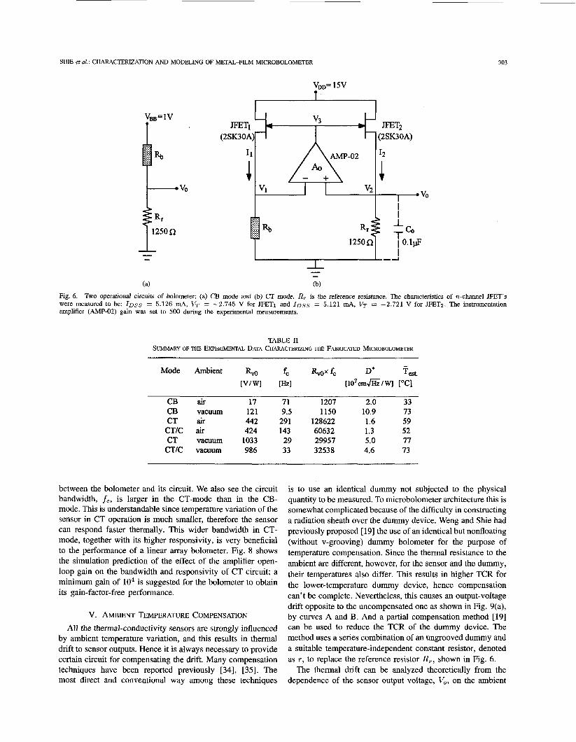
To test the effectiveness of the model established for mi- crobolometer, examples were used on the fabricated device with CB and CT circuits (as depicted in Fig. 6(aj and (b)), and either evacuated or not. As shown in Fig. 6(bj, constant temperature circuit given by Mastrangelo and Muller was used [17], except that the dual MOS in their circuit were replaced by a pair of n-channel JFET. The JFET’s were operated in saturation region as voltage-controlled current sources. As shown in Fig. 6(b), the instrumentation amplifier (AMP-02) forces the voltages on RI, sensor (K) and R, reference (VZ) to be virtually equal. Since the two JFET’s are a matching pair, the currents in the two resistors are also nearly equal. This makes the sensors in a quasiconstant-resistance (or constant- temperature) state latched at the reference resistance, R,. A suitable output capacitor, CO, is sometimes connected for purposes of signal stabilization and bandwidth-tuning. As will be described, the capacitors can affect the measured char- acteristics. For simulation purpose, the characteristics of the n-channel JFET’s, the amplifier, and the sensor resistance were measured as accurately as possible with precision instruments.
Fig. 7(a) and (b) show the frequency responses measured under six different conditions for a sample B chosen ran- domly from our fabricated device. Good agreement is obtained between the experimental data (points) and the simulations (solid lines). During the simulations the value of absorptance a was required to adjust for beat fitting. This is because of a different sample from the one that produced Table I was used, and as explained, before the absorptance could be different from that listed in the table. One should note that a higher frequency attenuation of -40 dB/dec appears in curves denoted with CT/C, which have a capacitance CO loaded at the output of the CT circuit. The simulation is so accurate that even the small bump in the measurement located at cutoff- frequency region of CT/C curve in Fig. 7(a) can be described by the simulation with the proposed model. The frequency responsivities with the device operated in a vacuum of 5 x l o p 4 Torr [Fig. 7(b)] are notably (2 N 7 times) larger than that in the atmosphere [Fig. 7(a)]. This is expected from the reduction of device thermal conductance in a vacuum. The same but greater tendency ( ~ 7 times) is observed for the device thermal time constant, which was obtained from the fitting of the cutoff frequency. These evidence reassure the fact indicated by Fig. 4 that the gaseous thermal conduction dominates among all the heat-loss mechanisms while the bolometer is operating in the atmosphere. Best bolometer sensitivity therefore requires a vacuum environment of below 0.1 Torr for this device.
Table I1 summarizes the microbolometer characteristics ob- tained from sample B with the two test circuits, The highest responsivity 1033 V/W is obtained with CT-mode in the vacuum. Its normalized detectivity D* [33], however, is not the best among all the measurements. This is probably due to the noisy nature associated with the CT circuit. Operation with CB-mode in the vacuum appears to have a maximum D* of 1.09 x 10s cm&/W, which is nearly Johnson-noise limited. It is interesting to see the responsivity-bandwidth product of the bolometer, shown in the table. For the CB operation it is nearly a constant, but for the CT operation, the product increases in the atmosphere compared to that in the vacuum. This implies the complexity of feedback interaction
S H E et al.: CHARACTERIZATION AND MODELING OF METALFILM MICROBOLOMETER 303
vo
(2SK3OA) RET1 >+< I1 I A AMP-02
R,: 1250Q
.
Fig. 6. ’ h o operational circuits of bolometer: (a) CB mode and (b) CT mode. R, is the reference resistance. The characteristics of n-channel JET’S were measured to be: IDSS = 5.126 mA, VT = -2.745 V for JFETl and IDSS = 5.121 mA, VT = -2.721 V for JFET2. The instrumentation amplifier (AMP-02) gain was set to 500 during the experimental measurements.
TABLE I1 SUMMARY OF THE EXPERIMENTAL DATA CHARACTERIZING THE FABRICATED MICROBOLOMETER
- Mode Ambient Rvo fc Rvox fc D* Test.
[VIWI [HZ1 [~O’C~~~LIWJ [“C]
CB air 17 71 1207 2.0 33 CB vacuum 121 9.5 1150 10.9 73 CT air 442 291 128622 1.6 59 CT/C air 424 143 60632 1.3 52 CT vacuum 1033 29 29957 5.0 77
CT/C vacuum 986 33 32538 4.6 73
between the bolometer and its circuit. We also see the circuit bandwidth, f c , is larger in the CT-mode than in the CB- mode. This is understandable since temperature variation of the sensor in CT operation is much smaller, therefore the sensor can respond faster thermally. This wider bandwidth in CT- mode, together with its higher responsivity, is very beneficial to the performance of a linear array bolometer. Fig. 8 shows the simulation prediction of the effect of the amplifier open- loop gain on the bandwidth and responsivity of CT circuit; a minimum gain of lo4 is suggested for the bolometer to obtain its gain-factor-free performance.
V. AMBIENT TEMPERATURE COMPENSATION All the thermal-conductivity sensors are strongly influenced
by ambient temperature variation, and this results in thermal drift to sensor outputs. Hence it is always necessary to provide certain circuit for compensating the drift. Many compensation techniques have been reported previously [34], [35]. The most direct and conventional way among these techniques
is to use an identical dummy not subjected to the physical quantity to be measured. To microbolometer architecture this is somewhat complicated because of the difficulty in constructing a radiation sheath over the dummy device. Weng and Shie had previously proposed [ 191 the use of an identical but nonfloating (without v-grooving) dummy bolometer for the purpose of temperature compensation. Since the thermal resistance to the ambient are different, however, for the sensor and the dummy, their temperatures also differ. This results in higher TCR for the lower-temperature dummy device, hence compensation can’t be complete. Nevertheless, this causes an output-voltage drift opposite to the uncompensated one as shown in Fig. 9(a), by curves A and B. And a partial compensation method [19] can be used to reduce the TCR of the dummy device. The method uses a series combination of an ungrooved dummy and a suitable temperature-independent constant resistor, denoted as T , to replace the reference resistor R,, shown in Fig. 6.
The thermal drift can be analyzed theoretically from the dependence of the sensor output voltage, V,, on the ambient

304 JOURNAL OF MICROELECTROMECHANICAL SYSTEMS, VOL. 5, NO. 4, DECEMBER 1996
0 : CB Mode 0 : CT Mode A : CT/C Mode
1 on 1 Cl0 10' 102 1 o3 1 o4
Frequency [Hz]
(a)
\ 1 o o L a ' * t , , , l ' ' . 1 . 1 . 1 1 1 n 0 -.J
100 10' 102 1 o3 1 o4
Frequency [Hz]
(b) Fig. 7. Comparkons between the simulation results (solid lines) and the experimental meaiiurements (points) of a device spectral responsivities (sample B): (a) in the air and (b) in the vacuum of 5 x Torr. For best matching, the absorptance, a!, was adjusted to a value of 0.6 for all simulations. Notice that with a capacitor load the output responses (CTK curves) have a -40 dB/dec attenuation. The agreements are so good that even the small bump in the data at cutoff point of CT/C in the air can be reproduced by simulation.
temperature, Zva. For the simplest CB circuit of Fig. 6(a), it can be written as [151
d V , - VBBRbRrQo ao(T - T a ) - p[1 f ao(T - TO)] __ -~ -
dTa (Rb + RT)2 [1+ a o ( T a - TO)][l + ao(T - To)] (19)
500
F 5 400
h 2 2 300
Y
.e z 2 200 2
100
500 r l
400 A
300 3 8
200
100
10' 1 02 103 IO' 105 10% Open-Loop Gain of Amplifier (AMP-02)
Fig. 8. Simulation on the effect of open-loop gain of the feedback amplifier on the device responsivity and bandwidth in CT circuit. Both can be improved by increasing gain before saturated.
with p = 2, the ratio between two dummy components. The drift quantity is nulled when the following condition is held
For the CB operation in our experiment, T x 33"C, hence ,8 zz 0.02 theoretically. Complete elimination of the thermal offset can be reached, as proved experimentally by the blank circles in Fig. 9(a), with @ = 0.025. The solid line C in the figure shows the simulation result. One notes both the simulation and the experiment are in close agreement with the theory. The extracted parameters listed in Table I is used in the simulation. The experimental @ value of 0.025 is slightly smaller than that predicted by (20). This is because of the constant resistor, r , used in our experiment is not truly temperature independent. As shown also in Fig. 9(a), only 0.0875 pV/OC drift remains with the present partial compensation method. Comparably this is much smaller than 32 pV/"C and 574 pV/"C, respectively, obtained from the full-dummy compensation and uncompensated methods.
The same argument of the thermal drift phenomenon can be applied to the CT circuit of Fig. 6(b), though it: requires more subtle thinking. In any even, the partial compensation method for CB circuit described above is still effective. This is shown in Fig. 9(b) by our electrothermal SPICE simulation without experimental proof.
In array detectors, image uniformity is important. The am- bient temperature uniformity over the detector surface should be a major factor. The simple partial-compensation method described here therefore can be very useful for improving the thermal image quality, by allowing the opportunity of per- pixel compensation. One would also expect this method of representation to be used for other types of thermal sensor.
VI. CONCLUSION
The electrothermal SPICE model of a Pt-film microbolome- ter has been successfully established for simulation. The model includes two VCVS's to represent the influences of optical

S H E et al. : CHARACTERIZATION AND MODELING OF METAL-FILM MICROBOLOMETER 305
t y1
-150 -loo! \
,\ , , , , , , , , , , , I -400 ~ ” ” ~ ’ ~ ” “ ” ” ’ ‘ “ ~ ~ ~ 30 40 50 60 70
Ambient Temperature Ta [“C]
(b)
Fig. 9. Offset voltage as function of the ambient temperature with different compensations: (a) for CB mode and (b) for CT mode. The solid lines in figures represent that obtained by simulations with present bolometer model.
input and ambient temperature. Lumped parameters of the thermal device required for the simulation are systematically extracted from the experimental fittings and are consistent with the theory. Applications of the proposed model to simulate some bolometer driving circuits, as well as to the ambient drift phenomena, have proven to agree with the experimental measurements in high degree of accuracy. Among all the parameters, only the absorptance is required to be estimated for matching the data between the simulation and the experiment.
It has been proven in this report that the ambient temperature offset can be suppressed very efficiently by the partial compen- sation method proposed previously. This method is potentially useful for array detectors, because only two resistive elements are required for each pixel of an array. The real-estate and process demands in fabricating these detectors can be relaxed, if per-pixel compensation for ambient temperature drift is necessary. This improvement together with the advantage of temperature linearity of Pt-film resistance could make the bolometer very suitable for radiometric purposes.
From the experiment, one recognizes that the sensitivity with CT-in-vacuum is high enough for practical applications. Higher sensitivity could also be obtained, if 1) high TCR thermistor materials are used [36]-[38]; 2) the operational circuit is tuned to its optimal sensitivity; and 3) the device structure is re-designed to reach its radiation-loss limited configuration. All of these can be analyzed with the established electro-thermal SPICE model of the bolometer.
ACKNOWLEDGMENT
The authors would like to thank Opt0 Tech Corporation in Science Based Industry Park of Hsinchu, Taiwan, for the technical supports on device processing. They would also like to thank Dr. P. K. Weng for preparing the samples J. Shie for proofreading of the manuscript.
REFERENCES
K. C. Liddiard, “Thin-film resistance bolometer IR detectors,” Infrared Phys., vol. 24, pp. 57-64, 1984. E. R. Muller and F. Mast, “A new metal resistor bolometer for measuring vacuum ultraviolet and soft x radiation,” J. Appl. Phys., vol. 55, pp. 2635-2641, 1984. W. Lang and K. Kuhl, “A thin-film bolometer for radiation thermometsy at ambient temperature,” Sens. Actuators, vol. A21-A23, pp. 473-477, 1990. L. Brnnetti and E. Monticone, “Properties of nickel thin films on polyimide substrate for HF bolometer,” Meas. Sci. Technol., vol. 4, pp. 1244-1248, 1993. A. M. N. Lima, G. S. Deep, J. S. R. Neto, R. C. S. Freire, and P. C. Lobo, “Identification of thermal-resistive solar radiation sensors,” IEEE Trans. Instrum. Meas., vol. 43, pp. 133-138, 1994. R. A. Wood, C. J. Hand, and P. W. Kruse, “Integrated uncooled in- frared detector imaging array,” in IEEE Solid-state Sensor and Actuator Workshop, June 1992, pp. 132-135. R. E. Flannery and J. E. Miller, “Status of uncooled infrared imagers,” SPIE, vol. 1689, pp. 379-395, 1992. A. Tanaka, S. Matsumoto, N. Tsukamoto, S. Itoh, T. Endoh, A. Naka- zoto, Y. Kumazawa, M. Hijikawa, H. Gotoh, T. Tanaka, and N. Teranishi, “Silicon IC process compatible bolometer infrared focal plane array,” in 8th Int. Con$ Solid-state Sensors and Actuators and Eurosensors IX, Stockholm, Sweden, June 1995, pp. 632-635. P. Gray and D. J. Hamilton, “Analysis of electro-thermal integrated circuits,” IEEE J. Solid-state Circuits, vol. 6, pp. 8-14, 1971. S. S. Lee and D. 5. Allstot, “Electro-thermal simulation of integrated circuit,” ZEEE J. Solid-state Circuits, vol. 28, pp. 1283-1293, 1993. L. R. Gray, D. J. Hamilton, and J. D. Lieux, “Analysis and design of temperature stabilized substrate integrated circuits,” IEEE J. Solid-state Circuits, vol. 9, pp. 61-69, 1974. A. R. Hefner and D. L. Blackburn, “Thermal component models for electro-thermal network simulation,” in Ninth IEEE Semi-Therm Symp.,
N. R. Swart and A. Nathan, “Flow-rate microsensor modeling and optimization using SPICE,” Sens. Acruators, vol. A34, pp. 109-122, 1992. N. Swart, A. Nathan, M. Shams, and M. Parameswaran, “Numerical optimization of flow-rate microsensors using circuit simulation tools,” Tech. Dig. Transducers’91, 1991, pp. 26-29. C. H. Mastrangelo, “Thermal applications of microbridges,” Ph.D. dissertation, Univ. of Californnia, Berkeley, 1991. J. S. Shie and P. K. Weng, “Design considerations of metal-film bolometer with iilicromachined floating membrane,” Sens. Actuators,
C. H. Mastrangelo and R. S. Muller, “Microfabricated thermal absolute- pressure sensor with on-chip digital front-end processor,” IEEE J. Solid-state Circuits, vol. 26, pp. 1998-2007, 1991. J. F. Kreider, “A simple constant-temperature hot-wire anemometer,” IEEE Trans. Instrum. Meas., pp. 190-191, June 1973. P. K. Weng and J. S. Shie, “Micro-Pirani vacuum gauge,” Rev. Sci. Instrum., vol. 65, pp. 492-499, 1994. T. Ricolfi and J. Scholz, Sensors: A Comprehensive Survey, 161. 4, Thermal Sensors.
1993, pp. 88-98.
vol. A33, pp. 183-189, 1992.
New York VCH, 1990, ch. 3, p. 86-107.

306 JOURNAL OF MICROELECTROMECHANICAL SYSTEMS, VOL. 5, NO. 4, DECEMBER 1996
[21] S. Danyluk G. E. McGuire, K. M. Koliwad, and M. G. Yang, “Diffusion studies in Cr-Pt thin films using Auger electron spectroscopy,” Thin Solid Films, vol. 25, pp. 483-489, 1975.
[22] F. M. d’Heurle and J. E. E. Baglin, in Proc. 7th Int. Vacuum Congress and 3rd Int. Con$ Solid Surface, Vienna, Austria, 1977.
[23] N. F. Mott and H. Jones, The Theory of the Properties of Metals and Alloys.
[24] K. C. Liddliard, “Thin-film resistance bolometer IR detectors-U,’’ In- frared Phys., vol. 26, pp. 43-49, 1986.
[25] W. G. Baer, T. Hull, K. D. Wise, K. Najafi, and K. D. Wise, “A mul- tiplexed siliicon infrared thermal imager,” in Tech. Dig. Transducers ’91, 1991, pp. 631-634.
[26] J. Lu, B. Xiong, and C. Lin, “Structure and properties of silicon-metal thermopile,” Sens. Actuators A , vol. 35, pp. 217-220, 1993.
1271 W. Budde, Optical Radiation Measurements, Vol. 4: Physical Detectors
New York: Dover, 1958, ch. 7, p. 286302.
. .
[281
[291 New York: Wiley, 1962, ch. 1.
[30] Y. M. Chenl, J. S. Shie, and T. Hwang, “Parameter extraction of resistive
[3 11
of Optical Radition. New York: Academic, 1983. . R. D. Hudson, Infrared System Engineering. New York Wiley, 1969, ch. 2, p. 39-53. S. Dushmam, Scientific Foundations of Vacuum Techniaue, 2nd ed.
thermal serrsors,” to be published. C. H. Mastrangelo and R. S. Muller, “Design and performance of constant-temperature circuits for microbridge-sensor applications,” in Tech. Dig. Transducers’91, 1991, pp. 471-474.
1321 N. R. Swart and A. Nathan. “Coupled electrothermal modeling of - - microheaters using SPICE,” IEEE Trins. Electron Devices, vol. 41: pp. 920-925, June 1994.
1331 R. H. Kingston, Detection of Optical and Infrared Radiation. New ” . . .
York: Springer, 1978, ch. 2. I341 S. Kalivumvaradan, P. Sankaran. and V. G. K. Murti. “A new com-
I I - - pensation scheme for thermistors and its implementation for response linearization over a wide temperature range,” IEEE Trans. Instrum. Meas., vol. 42, pp. 952-956, 1993.
[35] M. Matsuno, S. Adachi, M. Nakayama, and K. Watanabe, “A bridge circuit for temuerature drift cancellation.” IEEE Trans. Inshum. Meas., vol. 42, pp. 8?0-872, 1993.
[361 E. Iborra, A. Sanz-Hervas, T. Rodriguez, M. A. Ochando and A.P. . . Navarro, “High sensitivity bolometers development,” Rev. Sci. Instrum., vol. 63, pp. 47084710, 1992.
[37] T. Mori, T. Kudoh, K. Komatsu, and M. Kimura, “Vacuum-encapsulated thermistor bolometer type miniature infrared sensor,” in Proc. IEEE MEMS, 19!>4, vol. 3, pp. 257-262.
[38] P. Umadevi, C. L. Nagendra, and G. K. M. Thutupalli, “Structural, electrical and infrared optical properties of vanadium pentoxide thick- film thermistors,” Sens. Actuators A, vol. 39, pp. 5949, 1993.
Jin-Shown Shie received the B.S.E.E. degree from National Cheng Kung University, Taiwan, R.O.C., in 1965, and the M.S.E.E. degree from National Chiao Tung University, Hsinchu, Taiwan, in 1968. In 1972, he received the Ph.D. degree from the Department of Materials Science, State University of New York (SUNY) at Stony Brook.
Since then, he has been with the National Chiao Tung University. He is currently a Faculty Member, Institute of Electro-Optical Engineering. His present interest is in the field of microsensor technolom.
Yeong-Maw Chen (S’96) received the B.S. de- gree in physics from National Central University of Taiwan, R.O.C., in 1981 and the M.S. degree in electro-optical engineering from National Chiao Tung University, Hsinchn, Taiwan, in 1983. He is currently a Ph.D. candidate in the Institute of Electro-Optical Engineering, National Chiao Tung University, majoring in uncooled infrared detection.
Since then, he has been working in CSIST on radar system analysis and design.
Mang Ou-Yang (S’96) received the B.S. degree in control engineering in 1991, and the M.S. degree in electro-optical engineering in 1993 from National Chiao Tung University, Hsinchu, Taiwan, R.O.C., where he is currently pursuing the Ph.D. degree.
His research is in the fabrication of thermal sensors and the readout electronics.
Bruce C. S. Chou (S’96) received the B.S. de- gree in physics from Tung Hai University, Taiwan, R.O.C., in 1989 and the M.S. degree in nuclear science from National Tsing Hua University in 1991, majoring in high vacuum measurement. He is currently pursuing the Ph.D. degree at the Insti- tute of Electro-Optical Engineering, National Chiao Tung University, Hsinchu, Taiwan.
He is interested in the design and fabrication of micro-vacuum sensors and micromachining technol- ogy.
particularly in fabrication by surface micromachining of uncooled thermal infrared FPA detectors and IR system design.