ultra low power arm cortex-m4f mcu with integrated power ... · ultra low power arm cortex-m4f mcu...
TRANSCRIPT

Ultra Low Power ARM Cortex-M4F MCU with Integrated Power Management
Data Sheet ADuCM4050
Rev. A Document Feedback Information furnished by Analog Devices is believed to be accurate and reliable. However, no responsibility is assumed by Analog Devices for its use, nor for any infringements of patents or other rights of third parties that may result from its use. Specifications subject to change without notice. No license is granted by implication or otherwise under any patent or patent rights of Analog Devices. Trademarks and registered trademarks are the property of their respective owners.
One Technology Way, P.O. Box 9106, Norwood, MA 02062-9106, U.S.A. Tel: 781.329.4700 ©2018–2019 Analog Devices, Inc. All rights reserved. Technical Support www.analog.com
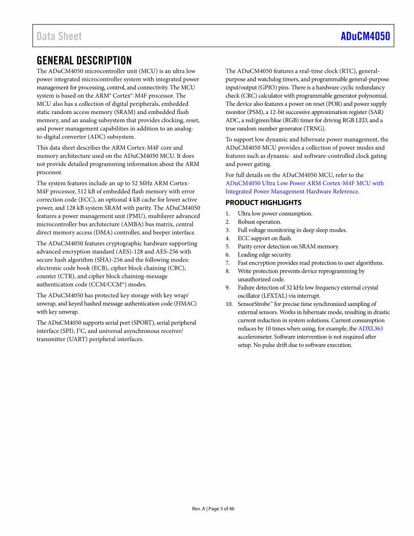
FEATURES EEMBC ULPMark™-CP score (3 V): 189 Ultra low power active and hibernate modes Active mode dynamic current: 41 µA/MHz (typical) Flexi mode: 400 µA (typical) Hibernate mode: 0.65 µA (typical) Shutdown mode: 50 nA (typical) Shutdown mode (fast wake-up): 0.20 µA (typical) ARM Cortex-M4F processor at 52 MHz with FPU, MPU, ITM
with SWD interface Power management Single-supply operation (connected to VBAT pins): 1.74 V to
3.6 V Optional buck converter for improved efficiency Memory options 512 kB of embedded flash memory with ECC 4 kB of cache memory to reduce active power 128 kB of configurable system SRAM with parity Safety
Watchdog with dedicated on-chip oscillator Hardware CRC with programmable polynomial Multiparity bit protected SRAM ECC protected embedded flash
Security Hardware cryptographic accelerator supporting AES-128,
AES-256, and SHA-256 Protected key storage in flash, SHA-256-based keyed HMAC and key wrap and unwrap User code protection TRNG
Digital peripherals 3 SPI interfaces to enable glueless interface to sensors,
radios, and converters 1 I2C and 2 UART peripheral interfaces SPORT for natively interfacing with converters and radios
Programmable GPIOs (44 in LFCSP and 51 in WLCSP) 3 general-purpose timers with PWM support RGB timer for driving RGB LED RTC0 for time keeping RTC1 with SensorStrobe and time stamping Programmable beeper 27-channel DMA controller
Clocking features 26 MHz clock: on-chip oscillator, external crystal oscillator,
SYS_CLKIN for external clock, and integrated PLL 32 kHz clock: on-chip oscillator and low power crystal
oscillator Clock fail detection for external crystals
Analog peripherals 12-bit SAR ADC, 1.8 MSPS, 8 channels, and digital comparator
APPLICATIONS Internet of Things (IoT) Smart agriculture, smart building, smart metering, smart
city, smart machine, and sensor network Wearables Fitness and clinical Machine learning and neural networks
FUNCTIONAL BLOCK DIAGRAM
AHB–APBBRIDGE
DATA SRAM/INSTRUCTION
SRAM/CACHE (128kB)
DMA
SERIAL WIREITM TRACE
ARMCORTEX–M4F
NVICLFOSC
HFOSC
LFXTAL
HFXTAL
PLL
PWR MGT
HP BUCK
WICMPU FPU
MULTI-LAYERAMBABUS
MATRIX
52MHz CORE RATE
TMR0
TMR2
UART1
TRNG
UART0
I2C
SPORT
SPIH
CRYPTO(AES-128, AES-256,
SHA 256)KEYED HMAC
KEY WRAP–UNWRAPPROTECTED
KEY STORAGE
SPI1
ADC CONTROLLER
ADCTEMP SENSORREF BUFFER
SPI0PROGRAMMABLECRC POLYNOMIAL
FLASH (512kB)
TMR1
RGB TMR
RTC0
WDT
RTC1
BEEPER GPIO
1474
5-00
1
Figure 1.

ADuCM4050 Data Sheet
Rev. A | Page 2 of 46
TABLE OF CONTENTS Features .............................................................................................. 1 Applications ....................................................................................... 1 Functional Block Diagram................................................................. 1 Revision History ............................................................................... 2 General Description ......................................................................... 3 Product Highlights ........................................................................... 3 Specifications ..................................................................................... 4
Operating Conditions and Electrical Characteristics .............. 4 Embedded Flash Specifications .................................................. 4 Power Supply Current Specifications ......................................... 5 ADC Specifications .................................................................... 10 Temperature Sensor Specifications .......................................... 11 System Clocks ............................................................................. 12 Timing Specifications ................................................................ 13
Absolute Maximum Ratings .......................................................... 20 Thermal Resistance .................................................................... 20 ESD Caution ................................................................................ 20
Pin Configuration and Function Descriptions ........................... 21 Typical Performance Characteristics ........................................... 26
Theory of Operation ...................................................................... 28 ARM Cortex-M4F Processor .................................................... 28 Memory Architecture ................................................................ 29 System Integration Features ...................................................... 30 On-Chip Peripheral Features .................................................... 35 Development Support ................................................................ 36 Reference Designs ...................................................................... 36 Security Features Disclaimer .................................................... 36 MCU Test Conditions ................................................................ 36 Driver Types ................................................................................ 36 EEMBC ULPMark™-CP Score .................................................. 37
GPIO Multiplexing ......................................................................... 38 Applications Information .............................................................. 40 Silicon Anomaly ............................................................................. 43
ADuCM4050 Functionality Issues ........................................... 43 Functionality Issues .................................................................... 43 Section 1. ADuCM4050 Functionality Issues......................... 44
Outline Dimensions ....................................................................... 45 Ordering Guide .......................................................................... 46
REVISION HISTORY 4/2019—Rev. 0 to Rev. A Change to Crystal Equivalent Series Resistance Parameter, Table 10 ............................................................................................ 12 Updated Outline Dimensions ....................................................... 45
6/2018—Revision 0: Initial Version
Data Sheet ADuCM4050
Rev. A | Page 3 of 46
GENERAL DESCRIPTION The ADuCM4050 microcontroller unit (MCU) is an ultra low power integrated microcontroller system with integrated power management for processing, control, and connectivity. The MCU system is based on the ARM® Cortex®-M4F processor. The MCU also has a collection of digital peripherals, embedded static random access memory (SRAM) and embedded flash memory, and an analog subsystem that provides clocking, reset, and power management capabilities in addition to an analog-to-digital converter (ADC) subsystem.
This data sheet describes the ARM Cortex-M4F core and memory architecture used on the ADuCM4050 MCU. It does not provide detailed programming information about the ARM processor.
The system features include an up to 52 MHz ARM Cortex-M4F processor, 512 kB of embedded flash memory with error correction code (ECC), an optional 4 kB cache for lower active power, and 128 kB system SRAM with parity. The ADuCM4050 features a power management unit (PMU), multilayer advanced microcontroller bus architecture (AMBA) bus matrix, central direct memory access (DMA) controller, and beeper interface.
The ADuCM4050 features cryptographic hardware supporting advanced encryption standard (AES)-128 and AES-256 with secure hash algorithm (SHA)-256 and the following modes: electronic code book (ECB), cipher block chaining (CBC), counter (CTR), and cipher block chaining-message authentication code (CCM/CCM*) modes.
The ADuCM4050 has protected key storage with key wrap/ unwrap, and keyed hashed message authentication code (HMAC) with key unwrap.
The ADuCM4050 supports serial port (SPORT), serial peripheral interface (SPI), I2C, and universal asynchronous receiver/ transmitter (UART) peripheral interfaces.
The ADuCM4050 features a real-time clock (RTC), general-purpose and watchdog timers, and programmable general-purpose input/output (GPIO) pins. There is a hardware cyclic redundancy check (CRC) calculator with programmable generator polynomial. The device also features a power on reset (POR) and power supply monitor (PSM), a 12-bit successive approximation register (SAR) ADC, a red/green/blue (RGB) timer for driving RGB LED, and a true random number generator (TRNG).
To support low dynamic and hibernate power management, the ADuCM4050 MCU provides a collection of power modes and features such as dynamic- and software-controlled clock gating and power gating.
For full details on the ADuCM4050 MCU, refer to the ADuCM4050 Ultra Low Power ARM Cortex-M4F MCU with Integrated Power Management Hardware Reference.
PRODUCT HIGHLIGHTS 1. Ultra low power consumption. 2. Robust operation. 3. Full voltage monitoring in deep sleep modes. 4. ECC support on flash. 5. Parity error detection on SRAM memory. 6. Leading edge security. 7. Fast encryption provides read protection to user algorithms. 8. Write protection prevents device reprogramming by
unauthorized code. 9. Failure detection of 32 kHz low frequency external crystal
oscillator (LFXTAL) via interrupt. 10. SensorStrobe™ for precise time synchronized sampling of
external sensors. Works in hibernate mode, resulting in drastic current reduction in system solutions. Current consumption reduces by 10 times when using, for example, the ADXL363 accelerometer. Software intervention is not required after setup. No pulse drift due to software execution.
ADuCM4050 Data Sheet
Rev. A | Page 4 of 46
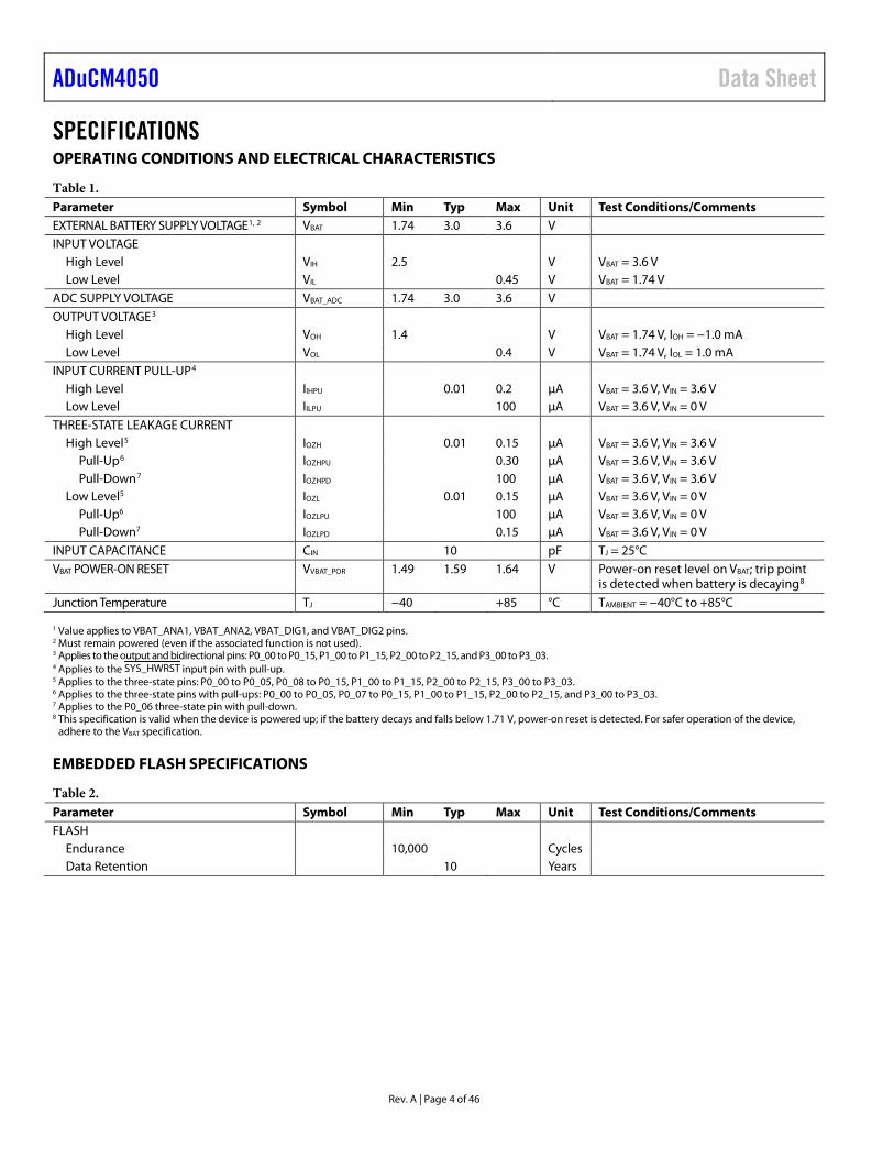
SPECIFICATIONS OPERATING CONDITIONS AND ELECTRICAL CHARACTERISTICS
Table 1. Parameter Symbol Min Typ Max Unit Test Conditions/Comments EXTERNAL BATTERY SUPPLY VOLTAGE1, 2 VBAT 1.74 3.0 3.6 V INPUT VOLTAGE
High Level VIH 2.5 V VBAT = 3.6 V Low Level VIL 0.45 V VBAT = 1.74 V
ADC SUPPLY VOLTAGE VBAT_ADC 1.74 3.0 3.6 V OUTPUT VOLTAGE3
High Level VOH 1.4 V VBAT = 1.74 V, IOH = −1.0 mA Low Level VOL 0.4 V VBAT = 1.74 V, IOL = 1.0 mA
INPUT CURRENT PULL-UP4 High Level IIHPU 0.01 0.2 µA VBAT = 3.6 V, VIN = 3.6 V Low Level IILPU 100 µA VBAT = 3.6 V, VIN = 0 V
THREE-STATE LEAKAGE CURRENT High Level5 IOZH 0.01 0.15 µA VBAT = 3.6 V, VIN = 3.6 V
Pull-Up6 IOZHPU 0.30 µA VBAT = 3.6 V, VIN = 3.6 V Pull-Down7 IOZHPD 100 µA VBAT = 3.6 V, VIN = 3.6 V
Low Level5 IOZL 0.01 0.15 µA VBAT = 3.6 V, VIN = 0 V Pull-Up6 IOZLPU 100 µA VBAT = 3.6 V, VIN = 0 V Pull-Down7 IOZLPD 0.15 µA VBAT = 3.6 V, VIN = 0 V
INPUT CAPACITANCE CIN 10 pF TJ = 25°C VBAT POWER-ON RESET VVBAT_POR 1.49 1.59 1.64 V Power-on reset level on VBAT; trip point
is detected when battery is decaying8 Junction Temperature TJ −40 +85 °C TAMBIENT = −40°C to +85°C 1 Value applies to VBAT_ANA1, VBAT_ANA2, VBAT_DIG1, and VBAT_DIG2 pins. 2 Must remain powered (even if the associated function is not used). 3 Applies to the output and bidirectional pins: P0_00 to P0_15, P1_00 to P1_15, P2_00 to P2_15, and P3_00 to P3_03. 4 Applies to the SYS_HWRST input pin with pull-up. 5 Applies to the three-state pins: P0_00 to P0_05, P0_08 to P0_15, P1_00 to P1_15, P2_00 to P2_15, P3_00 to P3_03. 6 Applies to the three-state pins with pull-ups: P0_00 to P0_05, P0_07 to P0_15, P1_00 to P1_15, P2_00 to P2_15, and P3_00 to P3_03. 7 Applies to the P0_06 three-state pin with pull-down. 8 This specification is valid when the device is powered up; if the battery decays and falls below 1.71 V, power-on reset is detected. For safer operation of the device,
adhere to the VBAT specification.
EMBEDDED FLASH SPECIFICATIONS
Table 2. Parameter Symbol Min Typ Max Unit Test Conditions/Comments FLASH
Endurance 10,000 Cycles Data Retention 10 Years
Data Sheet ADuCM4050
Rev. A | Page 5 of 46
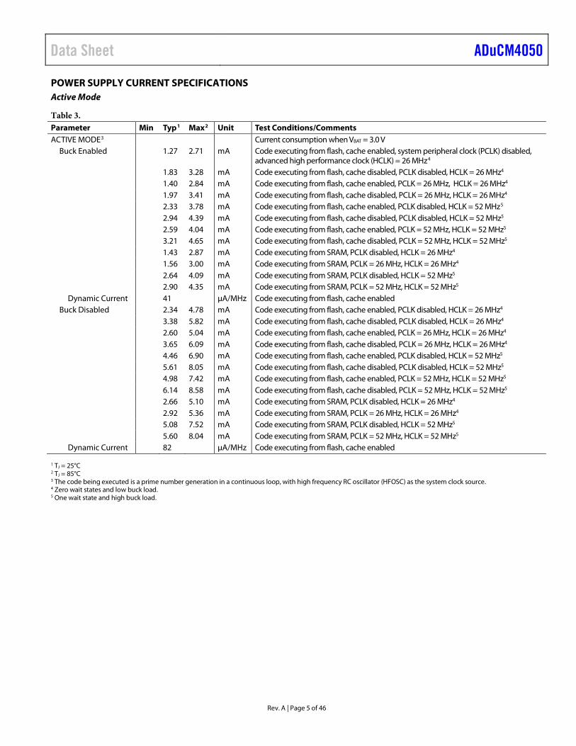
POWER SUPPLY CURRENT SPECIFICATIONS Active Mode
Table 3. Parameter Min Typ1 Max2 Unit Test Conditions/Comments ACTIVE MODE3 Current consumption when VBAT = 3.0 V
Buck Enabled 1.27 2.71 mA Code executing from flash, cache enabled, system peripheral clock (PCLK) disabled, advanced high performance clock (HCLK) = 26 MHz4
1.83 3.28 mA Code executing from flash, cache disabled, PCLK disabled, HCLK = 26 MHz4 1.40 2.84 mA Code executing from flash, cache enabled, PCLK = 26 MHz, HCLK = 26 MHz4 1.97 3.41 mA Code executing from flash, cache disabled, PCLK = 26 MHz, HCLK = 26 MHz4 2.33 3.78 mA Code executing from flash, cache enabled, PCLK disabled, HCLK = 52 MHz5 2.94 4.39 mA Code executing from flash, cache disabled, PCLK disabled, HCLK = 52 MHz5 2.59 4.04 mA Code executing from flash, cache enabled, PCLK = 52 MHz, HCLK = 52 MHz5 3.21 4.65 mA Code executing from flash, cache disabled, PCLK = 52 MHz, HCLK = 52 MHz5 1.43 2.87 mA Code executing from SRAM, PCLK disabled, HCLK = 26 MHz4 1.56 3.00 mA Code executing from SRAM, PCLK = 26 MHz, HCLK = 26 MHz4 2.64 4.09 mA Code executing from SRAM, PCLK disabled, HCLK = 52 MHz5 2.90 4.35 mA Code executing from SRAM, PCLK = 52 MHz, HCLK = 52 MHz5
Dynamic Current 41 µA/MHz Code executing from flash, cache enabled Buck Disabled 2.34 4.78 mA Code executing from flash, cache enabled, PCLK disabled, HCLK = 26 MHz4
3.38 5.82 mA Code executing from flash, cache disabled, PCLK disabled, HCLK = 26 MHz4 2.60 5.04 mA Code executing from flash, cache enabled, PCLK = 26 MHz, HCLK = 26 MHz4 3.65 6.09 mA Code executing from flash, cache disabled, PCLK = 26 MHz, HCLK = 26 MHz4 4.46 6.90 mA Code executing from flash, cache enabled, PCLK disabled, HCLK = 52 MHz5 5.61 8.05 mA Code executing from flash, cache disabled, PCLK disabled, HCLK = 52 MHz5 4.98 7.42 mA Code executing from flash, cache enabled, PCLK = 52 MHz, HCLK = 52 MHz5 6.14 8.58 mA Code executing from flash, cache disabled, PCLK = 52 MHz, HCLK = 52 MHz5 2.66 5.10 mA Code executing from SRAM, PCLK disabled, HCLK = 26 MHz4 2.92 5.36 mA Code executing from SRAM, PCLK = 26 MHz, HCLK = 26 MHz4 5.08 7.52 mA Code executing from SRAM, PCLK disabled, HCLK = 52 MHz5 5.60 8.04 mA Code executing from SRAM, PCLK = 52 MHz, HCLK = 52 MHz5
Dynamic Current 82 µA/MHz Code executing from flash, cache enabled 1 TJ = 25°C 2 TJ = 85°C 3 The code being executed is a prime number generation in a continuous loop, with high frequency RC oscillator (HFOSC) as the system clock source. 4 Zero wait states and low buck load. 5 One wait state and high buck load.
ADuCM4050 Data Sheet
Rev. A | Page 6 of 46
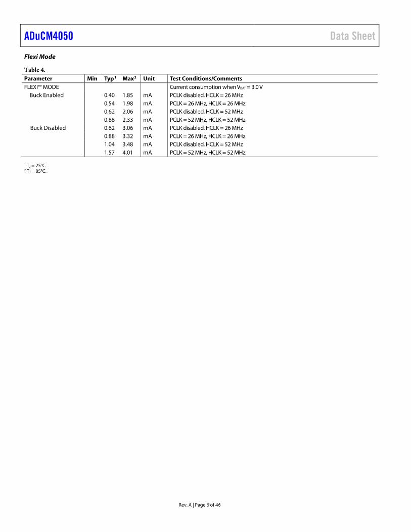
Flexi Mode
Table 4. Parameter Min Typ1 Max2 Unit Test Conditions/Comments FLEXI™ MODE Current consumption when VBAT = 3.0 V
Buck Enabled 0.40 1.85 mA PCLK disabled, HCLK = 26 MHz 0.54 1.98 mA PCLK = 26 MHz, HCLK = 26 MHz 0.62 2.06 mA PCLK disabled, HCLK = 52 MHz 0.88 2.33 mA PCLK = 52 MHz, HCLK = 52 MHz
Buck Disabled 0.62 3.06 mA PCLK disabled, HCLK = 26 MHz 0.88 3.32 mA PCLK = 26 MHz, HCLK = 26 MHz 1.04 3.48 mA PCLK disabled, HCLK = 52 MHz 1.57 4.01 mA PCLK = 52 MHz, HCLK = 52 MHz 1 TJ = 25°C. 2 TJ = 85°C.
Data Sheet ADuCM4050
Rev. A | Page 7 of 46
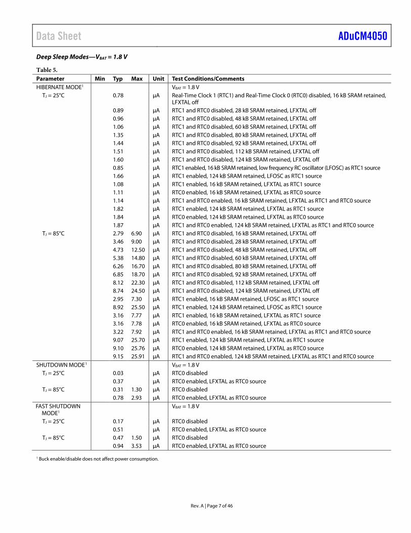
Deep Sleep Modes—VBAT = 1.8 V
Table 5. Parameter Min Typ Max Unit Test Conditions/Comments HIBERNATE MODE1 VBAT = 1.8 V
TJ = 25°C 0.78 µA Real-Time Clock 1 (RTC1) and Real-Time Clock 0 (RTC0) disabled, 16 kB SRAM retained, LFXTAL off
0.89 µA RTC1 and RTC0 disabled, 28 kB SRAM retained, LFXTAL off 0.96 µA RTC1 and RTC0 disabled, 48 kB SRAM retained, LFXTAL off 1.06 µA RTC1 and RTC0 disabled, 60 kB SRAM retained, LFXTAL off 1.35 µA RTC1 and RTC0 disabled, 80 kB SRAM retained, LFXTAL off 1.44 µA RTC1 and RTC0 disabled, 92 kB SRAM retained, LFXTAL off 1.51 µA RTC1 and RTC0 disabled, 112 kB SRAM retained, LFXTAL off 1.60 µA RTC1 and RTC0 disabled, 124 kB SRAM retained, LFXTAL off 0.85 µA RTC1 enabled, 16 kB SRAM retained, low frequency RC oscillator (LFOSC) as RTC1 source 1.66 µA RTC1 enabled, 124 kB SRAM retained, LFOSC as RTC1 source 1.08 µA RTC1 enabled, 16 kB SRAM retained, LFXTAL as RTC1 source 1.11 µA RTC0 enabled, 16 kB SRAM retained, LFXTAL as RTC0 source 1.14 µA RTC1 and RTC0 enabled, 16 kB SRAM retained, LFXTAL as RTC1 and RTC0 source 1.82 µA RTC1 enabled, 124 kB SRAM retained, LFXTAL as RTC1 source 1.84 µA RTC0 enabled, 124 kB SRAM retained, LFXTAL as RTC0 source 1.87 µA RTC1 and RTC0 enabled, 124 kB SRAM retained, LFXTAL as RTC1 and RTC0 source TJ = 85°C 2.79 6.90 µA RTC1 and RTC0 disabled, 16 kB SRAM retained, LFXTAL off 3.46 9.00 µA RTC1 and RTC0 disabled, 28 kB SRAM retained, LFXTAL off 4.73 12.50 µA RTC1 and RTC0 disabled, 48 kB SRAM retained, LFXTAL off 5.38 14.80 µA RTC1 and RTC0 disabled, 60 kB SRAM retained, LFXTAL off 6.26 16.70 µA RTC1 and RTC0 disabled, 80 kB SRAM retained, LFXTAL off 6.85 18.70 µA RTC1 and RTC0 disabled, 92 kB SRAM retained, LFXTAL off 8.12 22.30 µA RTC1 and RTC0 disabled, 112 kB SRAM retained, LFXTAL off 8.74 24.50 µA RTC1 and RTC0 disabled, 124 kB SRAM retained, LFXTAL off 2.95 7.30 µA RTC1 enabled, 16 kB SRAM retained, LFOSC as RTC1 source 8.92 25.50 µA RTC1 enabled, 124 kB SRAM retained, LFOSC as RTC1 source 3.16 7.77 µA RTC1 enabled, 16 kB SRAM retained, LFXTAL as RTC1 source 3.16 7.78 µA RTC0 enabled, 16 kB SRAM retained, LFXTAL as RTC0 source 3.22 7.92 µA RTC1 and RTC0 enabled, 16 kB SRAM retained, LFXTAL as RTC1 and RTC0 source 9.07 25.70 µA RTC1 enabled, 124 kB SRAM retained, LFXTAL as RTC1 source 9.10 25.76 µA RTC0 enabled, 124 kB SRAM retained, LFXTAL as RTC0 source 9.15 25.91 µA RTC1 and RTC0 enabled, 124 kB SRAM retained, LFXTAL as RTC1 and RTC0 source
SHUTDOWN MODE1 VBAT = 1.8 V TJ = 25°C 0.03 µA RTC0 disabled 0.37 µA RTC0 enabled, LFXTAL as RTC0 source TJ = 85°C 0.31 1.30 µA RTC0 disabled 0.78 2.93 µA RTC0 enabled, LFXTAL as RTC0 source
FAST SHUTDOWN MODE1
VBAT = 1.8 V
TJ = 25°C 0.17 µA RTC0 disabled 0.51 µA RTC0 enabled, LFXTAL as RTC0 source TJ = 85°C 0.47 1.50 µA RTC0 disabled 0.94 3.53 µA RTC0 enabled, LFXTAL as RTC0 source
1 Buck enable/disable does not affect power consumption.
ADuCM4050 Data Sheet
Rev. A | Page 8 of 46
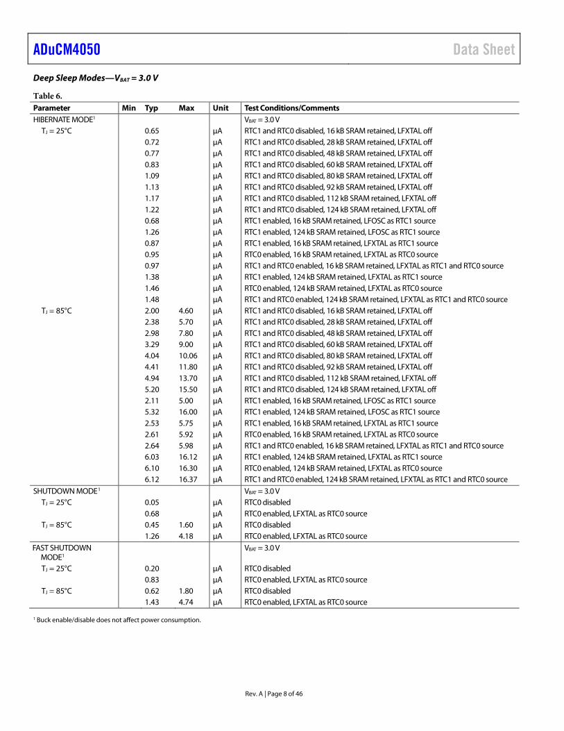
Deep Sleep Modes—VBAT = 3.0 V
Table 6. Parameter Min Typ Max Unit Test Conditions/Comments HIBERNATE MODE1 VBAT = 3.0 V
TJ = 25°C 0.65 µA RTC1 and RTC0 disabled, 16 kB SRAM retained, LFXTAL off 0.72 µA RTC1 and RTC0 disabled, 28 kB SRAM retained, LFXTAL off 0.77 µA RTC1 and RTC0 disabled, 48 kB SRAM retained, LFXTAL off 0.83 µA RTC1 and RTC0 disabled, 60 kB SRAM retained, LFXTAL off 1.09 µA RTC1 and RTC0 disabled, 80 kB SRAM retained, LFXTAL off 1.13 µA RTC1 and RTC0 disabled, 92 kB SRAM retained, LFXTAL off 1.17 µA RTC1 and RTC0 disabled, 112 kB SRAM retained, LFXTAL off 1.22 µA RTC1 and RTC0 disabled, 124 kB SRAM retained, LFXTAL off 0.68 µA RTC1 enabled, 16 kB SRAM retained, LFOSC as RTC1 source 1.26 µA RTC1 enabled, 124 kB SRAM retained, LFOSC as RTC1 source 0.87 µA RTC1 enabled, 16 kB SRAM retained, LFXTAL as RTC1 source 0.95 µA RTC0 enabled, 16 kB SRAM retained, LFXTAL as RTC0 source 0.97 µA RTC1 and RTC0 enabled, 16 kB SRAM retained, LFXTAL as RTC1 and RTC0 source 1.38 µA RTC1 enabled, 124 kB SRAM retained, LFXTAL as RTC1 source 1.46 µA RTC0 enabled, 124 kB SRAM retained, LFXTAL as RTC0 source 1.48 µA RTC1 and RTC0 enabled, 124 kB SRAM retained, LFXTAL as RTC1 and RTC0 source TJ = 85°C 2.00 4.60 µA RTC1 and RTC0 disabled, 16 kB SRAM retained, LFXTAL off 2.38 5.70 µA RTC1 and RTC0 disabled, 28 kB SRAM retained, LFXTAL off 2.98 7.80 µA RTC1 and RTC0 disabled, 48 kB SRAM retained, LFXTAL off 3.29 9.00 µA RTC1 and RTC0 disabled, 60 kB SRAM retained, LFXTAL off 4.04 10.06 µA RTC1 and RTC0 disabled, 80 kB SRAM retained, LFXTAL off 4.41 11.80 µA RTC1 and RTC0 disabled, 92 kB SRAM retained, LFXTAL off 4.94 13.70 µA RTC1 and RTC0 disabled, 112 kB SRAM retained, LFXTAL off 5.20 15.50 µA RTC1 and RTC0 disabled, 124 kB SRAM retained, LFXTAL off 2.11 5.00 µA RTC1 enabled, 16 kB SRAM retained, LFOSC as RTC1 source 5.32 16.00 µA RTC1 enabled, 124 kB SRAM retained, LFOSC as RTC1 source 2.53 5.75 µA RTC1 enabled, 16 kB SRAM retained, LFXTAL as RTC1 source 2.61 5.92 µA RTC0 enabled, 16 kB SRAM retained, LFXTAL as RTC0 source 2.64 5.98 µA RTC1 and RTC0 enabled, 16 kB SRAM retained, LFXTAL as RTC1 and RTC0 source 6.03 16.12 µA RTC1 enabled, 124 kB SRAM retained, LFXTAL as RTC1 source 6.10 16.30 µA RTC0 enabled, 124 kB SRAM retained, LFXTAL as RTC0 source 6.12 16.37 µA RTC1 and RTC0 enabled, 124 kB SRAM retained, LFXTAL as RTC1 and RTC0 source
SHUTDOWN MODE1 VBAT = 3.0 V TJ = 25°C 0.05 µA RTC0 disabled 0.68 µA RTC0 enabled, LFXTAL as RTC0 source TJ = 85°C 0.45 1.60 µA RTC0 disabled 1.26 4.18 µA RTC0 enabled, LFXTAL as RTC0 source
FAST SHUTDOWN MODE1
VBAT = 3.0 V
TJ = 25°C 0.20 µA RTC0 disabled 0.83 µA RTC0 enabled, LFXTAL as RTC0 source TJ = 85°C 0.62 1.80 µA RTC0 disabled 1.43 4.74 µA RTC0 enabled, LFXTAL as RTC0 source
1 Buck enable/disable does not affect power consumption.
Data Sheet ADuCM4050
Rev. A | Page 9 of 46
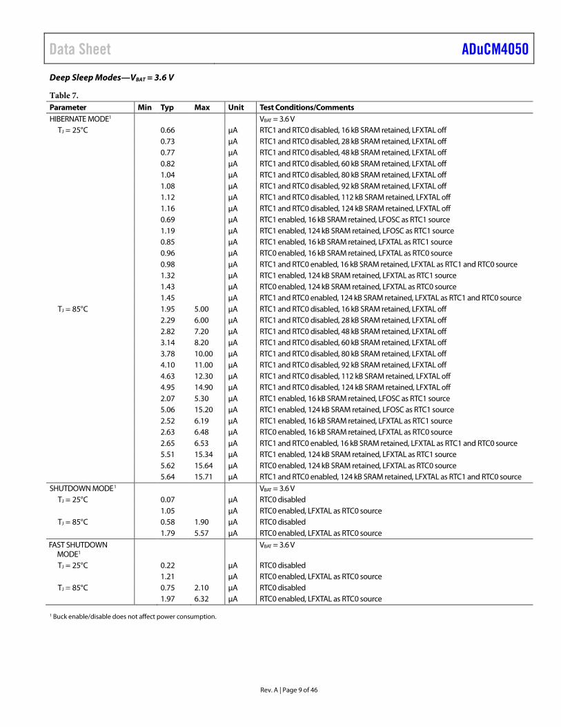
Deep Sleep Modes—VBAT = 3.6 V
Table 7. Parameter Min Typ Max Unit Test Conditions/Comments HIBERNATE MODE1 VBAT = 3.6 V
TJ = 25°C 0.66 µA RTC1 and RTC0 disabled, 16 kB SRAM retained, LFXTAL off 0.73 µA RTC1 and RTC0 disabled, 28 kB SRAM retained, LFXTAL off 0.77 µA RTC1 and RTC0 disabled, 48 kB SRAM retained, LFXTAL off 0.82 µA RTC1 and RTC0 disabled, 60 kB SRAM retained, LFXTAL off 1.04 µA RTC1 and RTC0 disabled, 80 kB SRAM retained, LFXTAL off 1.08 µA RTC1 and RTC0 disabled, 92 kB SRAM retained, LFXTAL off 1.12 µA RTC1 and RTC0 disabled, 112 kB SRAM retained, LFXTAL off 1.16 µA RTC1 and RTC0 disabled, 124 kB SRAM retained, LFXTAL off 0.69 µA RTC1 enabled, 16 kB SRAM retained, LFOSC as RTC1 source 1.19 µA RTC1 enabled, 124 kB SRAM retained, LFOSC as RTC1 source 0.85 µA RTC1 enabled, 16 kB SRAM retained, LFXTAL as RTC1 source 0.96 µA RTC0 enabled, 16 kB SRAM retained, LFXTAL as RTC0 source 0.98 µA RTC1 and RTC0 enabled, 16 kB SRAM retained, LFXTAL as RTC1 and RTC0 source 1.32 µA RTC1 enabled, 124 kB SRAM retained, LFXTAL as RTC1 source 1.43 µA RTC0 enabled, 124 kB SRAM retained, LFXTAL as RTC0 source 1.45 µA RTC1 and RTC0 enabled, 124 kB SRAM retained, LFXTAL as RTC1 and RTC0 source TJ = 85°C 1.95 5.00 µA RTC1 and RTC0 disabled, 16 kB SRAM retained, LFXTAL off 2.29 6.00 µA RTC1 and RTC0 disabled, 28 kB SRAM retained, LFXTAL off 2.82 7.20 µA RTC1 and RTC0 disabled, 48 kB SRAM retained, LFXTAL off 3.14 8.20 µA RTC1 and RTC0 disabled, 60 kB SRAM retained, LFXTAL off 3.78 10.00 µA RTC1 and RTC0 disabled, 80 kB SRAM retained, LFXTAL off 4.10 11.00 µA RTC1 and RTC0 disabled, 92 kB SRAM retained, LFXTAL off 4.63 12.30 µA RTC1 and RTC0 disabled, 112 kB SRAM retained, LFXTAL off 4.95 14.90 µA RTC1 and RTC0 disabled, 124 kB SRAM retained, LFXTAL off 2.07 5.30 µA RTC1 enabled, 16 kB SRAM retained, LFOSC as RTC1 source 5.06 15.20 µA RTC1 enabled, 124 kB SRAM retained, LFOSC as RTC1 source 2.52 6.19 µA RTC1 enabled, 16 kB SRAM retained, LFXTAL as RTC1 source 2.63 6.48 µA RTC0 enabled, 16 kB SRAM retained, LFXTAL as RTC0 source 2.65 6.53 µA RTC1 and RTC0 enabled, 16 kB SRAM retained, LFXTAL as RTC1 and RTC0 source 5.51 15.34 µA RTC1 enabled, 124 kB SRAM retained, LFXTAL as RTC1 source 5.62 15.64 µA RTC0 enabled, 124 kB SRAM retained, LFXTAL as RTC0 source 5.64 15.71 µA RTC1 and RTC0 enabled, 124 kB SRAM retained, LFXTAL as RTC1 and RTC0 source
SHUTDOWN MODE1 VBAT = 3.6 V TJ = 25°C 0.07 µA RTC0 disabled 1.05 µA RTC0 enabled, LFXTAL as RTC0 source TJ = 85°C 0.58 1.90 µA RTC0 disabled
1.79 5.57 µA RTC0 enabled, LFXTAL as RTC0 source FAST SHUTDOWN
MODE1 VBAT = 3.6 V
TJ = 25°C 0.22 µA RTC0 disabled 1.21 µA RTC0 enabled, LFXTAL as RTC0 source TJ = 85°C 0.75 2.10 µA RTC0 disabled 1.97 6.32 µA RTC0 enabled, LFXTAL as RTC0 source
1 Buck enable/disable does not affect power consumption.
ADuCM4050 Data Sheet
Rev. A | Page 10 of 46
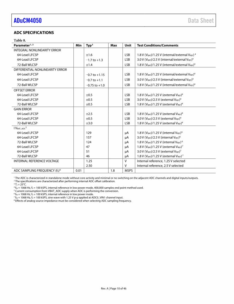
ADC SPECIFICATIONS
Table 8. Parameter1, 2 Min Typ3 Max Unit Test Conditions/Comments INTEGRAL NONLINEARITY ERROR
64-Lead LFCSP ±1.6 LSB 1.8 V (VBAT)/1.25 V (internal/external VREF) 4 64-Lead LFCSP −1.7 to +1.3 LSB 3.0 V (VBAT)/2.5 V (internal/external VREF)4
72-Ball WLCSP ±1.4 LSB 1.8 V (VBAT)/1.25 V (internal/external VREF)4 DIFFERENTIAL NONLINEARITY ERROR
64-Lead LFCSP −0.7 to +1.15 LSB 1.8 V (VBAT)/1.25 V (internal/external VREF)4
64-Lead LFCSP −0.7 to +1.1 LSB 3.0 V (VBAT)/2.5 V (internal/external VREF)4
72-Ball WLCSP −0.75 to +1.0 LSB 1.8 V (VBAT)/1.25 V (internal/external VREF)4
OFFSET ERROR 64-Lead LFCSP ±0.5 LSB 1.8 V (VBAT)/1.25 V (external VREF)4 64-Lead LFCSP ±0.5 LSB 3.0 V (VBAT)/2.5 V (external VREF)4 72-Ball WLCSP ±0.5 LSB 1.8 V (VBAT)/1.25 V (external VREF)4
GAIN ERROR 64-Lead LFCSP ±2.5 LSB 1.8 V (VBAT)/1.25 V (external VREF)4 64-Lead LFCSP ±0.5 LSB 3.0 V (VBAT)/2.5 V (external VREF)4 72-Ball WLCSP ±3.0 LSB 1.8 V (VBAT)/1.25 V (external VREF)4
I VBAT_ADC5
64-Lead LFCSP 129 µA 1.8 V (VBAT)/1.25 V (internal VREF)6 64-Lead LFCSP 157 µA 3.0 V (VBAT)/2.5 V (internal VREF)6 72-Ball WLCSP 124 µA 1.8 V (VBAT)/1.25 V (internal VREF) 6 64-Lead LFCSP 47 µA 1.8 V (VBAT)/1.25 V (external VREF)7 64-Lead LFCSP 51 µA 3.0 V (VBAT)/2.5 V (external VREF)7 72-Ball WLCSP 46 µA 1.8 V (VBAT)/1.25 V (external VREF) 7
INTERNAL REFERENCE VOLTAGE 1.25 V Internal reference, 1.25 V selected 2.50 V Internal reference, 2.5 V selected ADC SAMPLING FREQUENCY (fS)8 0.01 1.8 MSPS 1 The ADC is characterized in standalone mode without core activity and minimal or no switching on the adjacent ADC channels and digital inputs/outputs. 2 The specifications are characterized after performing internal ADC offset calibration. 3 TJ = 25°C. 4 fIN = 1068 Hz, fS = 100 kSPS, internal reference in low power mode, 400,000 samples end point method used. 5 Current consumption from VBAT_ADC supply when ADC is performing the conversion. 6 fIN = 1068 Hz, fS = 100 kSPS, internal reference in low power mode. 7 fIN = 1068 Hz, fS = 100 kSPS, sine wave with 1.25 V p-p applied at ADC0_VIN1 channel input. 8 Effects of analog source impedance must be considered when selecting ADC sampling frequency.
Data Sheet ADuCM4050
Rev. A | Page 11 of 46
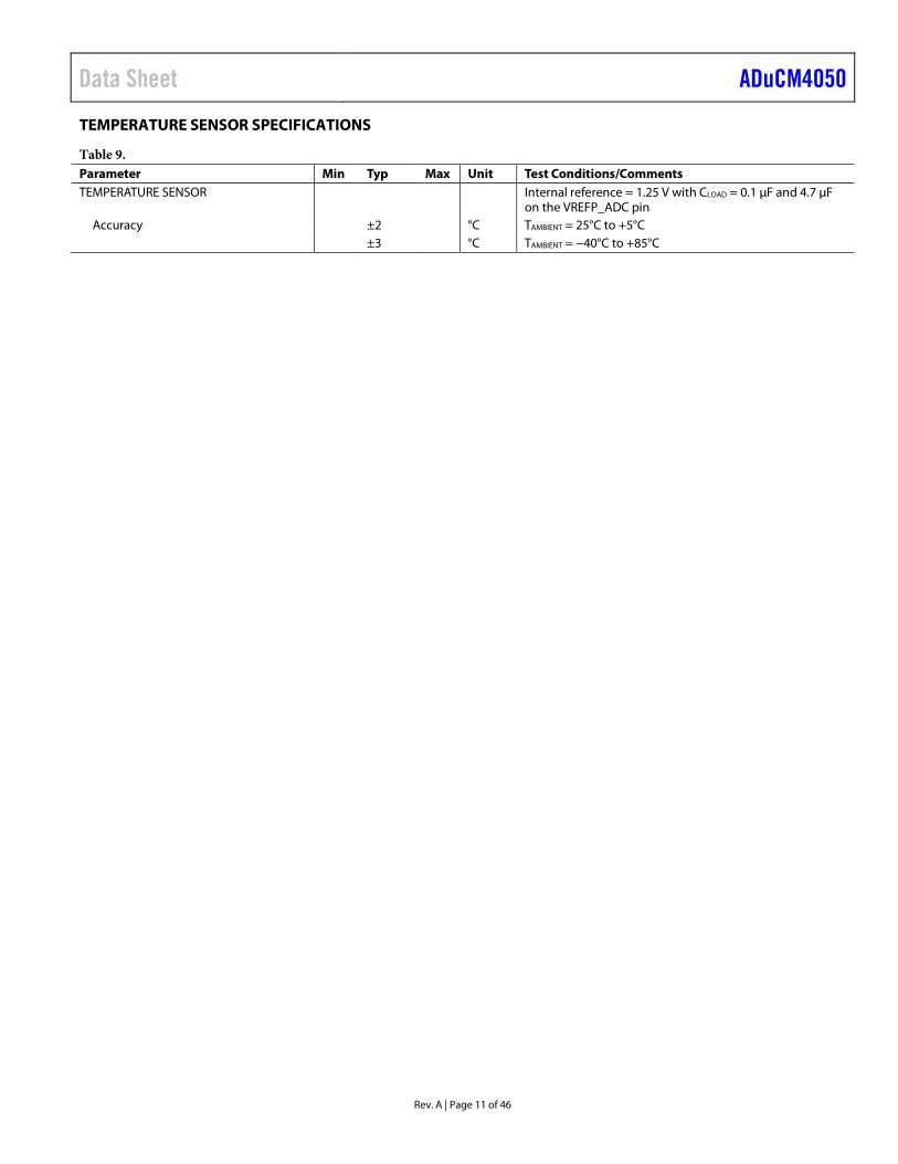
TEMPERATURE SENSOR SPECIFICATIONS
Table 9. Parameter Min Typ Max Unit Test Conditions/Comments TEMPERATURE SENSOR Internal reference = 1.25 V with CLOAD = 0.1 μF and 4.7 μF
on the VREFP_ADC pin Accuracy ±2 °C TAMBIENT = 25°C to +5°C
±3 °C TAMBIENT = −40°C to +85°C
ADuCM4050 Data Sheet
Rev. A | Page 12 of 46
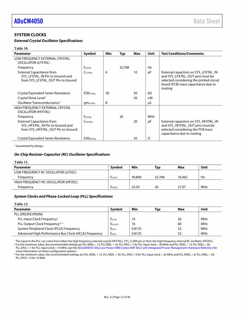
SYSTEM CLOCKS External Crystal Oscillator Specifications
Table 10. Parameter Symbol Min Typ Max Unit Test Conditions/Comments LOW FREQUENCY EXTERNAL CRYSTAL
OSCILLATOR (LFXTAL)
Frequency fLFXTAL 32,768 Hz External Capacitance from
SYS_LFXTAL_IN Pin to Ground and from SYS_LFXTAL_OUT Pin to Ground
CLFXTAL 6 10 pF External capacitors on SYS_LFXTAL_IN and SYS_LFXTAL_OUT pins must be selected considering the printed circuit board (PCB) trace capacitance due to routing
Crystal Equivalent Series Resistance ESRLFXTAL 30 50 kΩ Crystal Drive Level1 50 nW Oscillator Transconductance1 gmLFXTAL 8 µS
HIGH FREQUENCY EXTERNAL CRYSTAL OSCILLATOR (HFXTAL)
Frequency fHFXTAL 26 MHz External Capacitance from
SYS_HFXTAL_IN Pin to Ground and from SYS_HFXTAL_OUT Pin to Ground
CHFXTAL 20 pF External capacitors on SYS_HFXTAL_IN and SYS_HFXTAL_OUT pins must be selected considering the PCB trace capacitance due to routing
Crystal Equivalent Series Resistance ESRHFXTAL 50 Ω 1 Guaranteed by design.
On-Chip Resistor-Capacitor (RC) Oscillator Specifications
Table 11. Parameter Symbol Min Typ Max Unit LOW FREQUENCY RC OSCILLATOR (LFOSC)
Frequency fLFOSC 30,800 32,768 35,062 Hz HIGH FREQUENCY RC OSCILLATOR (HFOSC)
Frequency fHFOSC 25.03 26 27.07 MHz
System Clocks and Phase-Locked Loop (PLL) Specifications
Table 12. Parameter Symbol Min Typ Max Unit PLL SPECIFICATIONS
PLL Input Clock Frequency1 fPLLIN 16 26 MHz PLL Output Clock Frequency2, 3 fPLLOUT 16 60 MHz System Peripheral Clock (PCLK) Frequency fPCLK 0.8125 52 MHz Advanced High Performance Bus Clock (HCLK) Frequency fHCLK 0.8125 52 MHz
1 The input to the PLL can come from either the high frequency external crystal (HFXTAL), SYS_CLKIN pin or from the high frequency internal RC oscillator (HFOSC). 2 For the maximum value, the recommended settings are PLL MSEL = 13, PLL NSEL = 16, PLL DIV2 = 1 for PLL input clock = 26 MHz; and PLL MSEL = 13, PLL NSEL = 26,
PLL DIV2 = 1 for PLL input clock = 16 MHz; see the ADuCM4050 Ultra Low Power ARM Cortex-M4F MCU with Integrated Power Management Hardware Reference for more information on these configuration options.
3 For the minimum value, the recommended settings are PLL MSEL = 13, PLL NSEL = 30, PLL DIV2 = 0 for PLL input clock = 26 MHz; and PLL MSEL = 8, PLL NSEL = 30, PLL DIV2 = 0 for 16 MHz.
Data Sheet ADuCM4050
Rev. A | Page 13 of 46
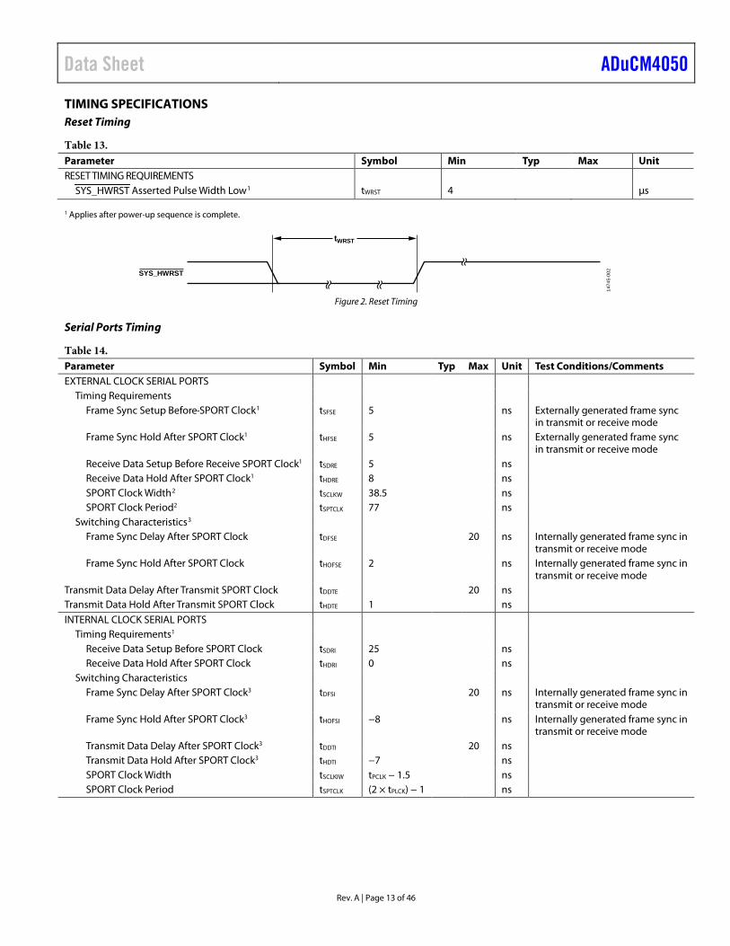
TIMING SPECIFICATIONS Reset Timing
Table 13. Parameter Symbol Min Typ Max Unit RESET TIMING REQUIREMENTS
SYS_HWRST Asserted Pulse Width Low1 tWRST 4 µs 1 Applies after power-up sequence is complete.
SYS_HWRST
tWRST
1474
5-00
2
Figure 2. Reset Timing
Serial Ports Timing
Table 14. Parameter Symbol Min Typ Max Unit Test Conditions/Comments EXTERNAL CLOCK SERIAL PORTS
Timing Requirements Frame Sync Setup Before SPORT Clock1 tSFSE 5 ns Externally generated frame sync
in transmit or receive mode Frame Sync Hold After SPORT Clock1 tHFSE 5 ns Externally generated frame sync
in transmit or receive mode Receive Data Setup Before Receive SPORT Clock1 tSDRE 5 ns Receive Data Hold After SPORT Clock1 tHDRE 8 ns SPORT Clock Width2 tSCLKW 38.5 ns SPORT Clock Period2 tSPTCLK 77 ns
Switching Characteristics3 Frame Sync Delay After SPORT Clock tDFSE 20 ns Internally generated frame sync in
transmit or receive mode Frame Sync Hold After SPORT Clock tHOFSE 2 ns Internally generated frame sync in
transmit or receive mode Transmit Data Delay After Transmit SPORT Clock tDDTE 20 ns Transmit Data Hold After Transmit SPORT Clock tHDTE 1 ns INTERNAL CLOCK SERIAL PORTS
Timing Requirements1 Receive Data Setup Before SPORT Clock tSDRI 25 ns Receive Data Hold After SPORT Clock tHDRI 0 ns
Switching Characteristics Frame Sync Delay After SPORT Clock3 tDFSI 20 ns Internally generated frame sync in
transmit or receive mode Frame Sync Hold After SPORT Clock3 tHOFSI −8 ns Internally generated frame sync in
transmit or receive mode Transmit Data Delay After SPORT Clock3 tDDTI 20 ns Transmit Data Hold After SPORT Clock3 tHDTI −7 ns SPORT Clock Width tSCLKIW tPCLK − 1.5 ns SPORT Clock Period tSPTCLK (2 × tPLCK) − 1 ns
ADuCM4050 Data Sheet
Rev. A | Page 14 of 46
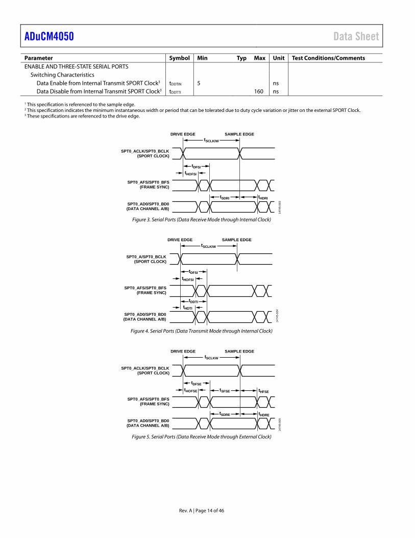
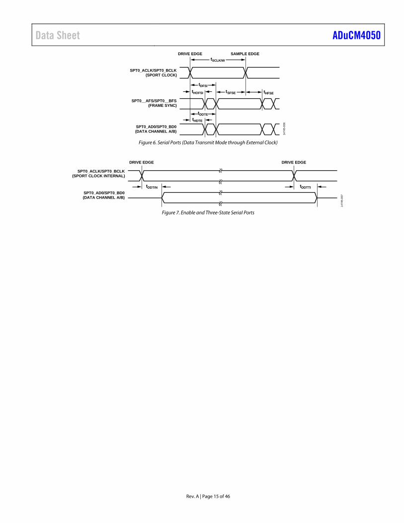
Parameter Symbol Min Typ Max Unit Test Conditions/Comments ENABLE AND THREE-STATE SERIAL PORTS
Switching Characteristics Data Enable from Internal Transmit SPORT Clock3 tDDTIN 5 ns Data Disable from Internal Transmit SPORT Clock3 tDDTTI 160 ns
1 This specification is referenced to the sample edge. 2 This specification indicates the minimum instantaneous width or period that can be tolerated due to duty cycle variation or jitter on the external SPORT Clock. 3 These specifications are referenced to the drive edge.
tSCLKIW
DRIVE EDGE
SPT0_ACLK/SPT0_BCLK(SPORT CLOCK)
SPT0_AFS/SPT0_BFS(FRAME SYNC)
SPT0_AD0/SPT0_BD0(DATA CHANNEL A/B)
SAMPLE EDGE
tHOFSI
tSDRI
tDFSI
tHDRI
1474
5-00
3
Figure 3. Serial Ports (Data Receive Mode through Internal Clock)
tSCLKIW
DRIVE EDGE
SPT0_A/SPT0_BCLK(SPORT CLOCK)
SPT0_AFS/SPT0_BFS(FRAME SYNC)
SPT0_AD0/SPT0_BD0(DATA CHANNEL A/B)
SAMPLE EDGE
tHOFSI
tDDTItHDTI
tDFSI14
745-
004
Figure 4. Serial Ports (Data Transmit Mode through Internal Clock)
tSCLKW
DRIVE EDGE
SPT0_ACLK/SPT0_BCLK(SPORT CLOCK)
SPT0_AFS/SPT0_BFS(FRAME SYNC)
SPT0_AD0/SPT0_BD0(DATA CHANNEL A/B)
SAMPLE EDGE
tHOFSE
tSDRE
tDFSE
tSFSE
tHDRE
tHFSE
1474
5-00
5
Figure 5. Serial Ports (Data Receive Mode through External Clock)
Data Sheet ADuCM4050
Rev. A | Page 15 of 46
tSFSE tHFSE
tSCLKIW
DRIVE EDGE
SPT0_ACLK/SPT0_BCLK(SPORT CLOCK)
SPT0__AFS/SPT0__BFS(FRAME SYNC)
SPT0_AD0/SPT0_BD0(DATA CHANNEL A/B)
SAMPLE EDGE
tHOFSI
tDDTEtHDTE
tDFSI
1474
5-00
6
Figure 6. Serial Ports (Data Transmit Mode through External Clock)
tDDTIN
DRIVE EDGE DRIVE EDGE
SPT0_ACLK/SPT0_BCLK(SPORT CLOCK INTERNAL)
SPT0_AD0/SPT0_BD0(DATA CHANNEL A/B)
tDDTTI
1474
5-00
7
Figure 7. Enable and Three-State Serial Ports

ADuCM4050 Data Sheet
Rev. A | Page 16 of 46
SPI Timing
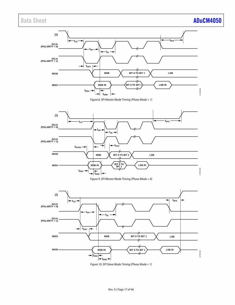
Table 15. Parameter1 Symbol Min Typ Max Unit SPI MASTER MODE TIMING
Timing Requirements Chip Select (CS) to Serial Clock (SCLK) Edge tCS (2 × tPCLK) − 6.5 ns SCLK Low Pulse Width tSL tPCLK − 3.5 ns SCLK High Pulse Width tSH tPCLK − 3.5 ns Data Input Setup Time Before SCLK Edge tDSU 5 ns Data Input Hold Time After SCLK Edge tDHD 20 ns
Switching Characteristics Data Output Valid After SCLK Edge tDAV 25 ns Data Output Setup Before SCLK Edge tDOSU tPCLK − 2.2 ns CS High After SCLK Edge tSFS tPCLK + 2 ns
High Speed SPI (SPIH) MASTER MODE TIMING Timing Requirements
CS to SCLK Edge tCS (2 × tPCLK) − 6.5 ns SCLK Low Pulse Width tSL tPCLK − 2 ns SCLK High Pulse Width tSH tPCLK − 2 ns Data Input Setup Time Before SCLK Edge tDSU 3.5 ns Data Input Hold Time After SCLK Edge tDHD 12 ns
Switching Characteristics Data Output Valid After SCLK Edge tDAV 12.5 ns Data Output Setup Before SCLK Edge tDOSU tPCLK − 2.2 ns CS High After SCLK Edge tSFS tPCLK + 2 ns
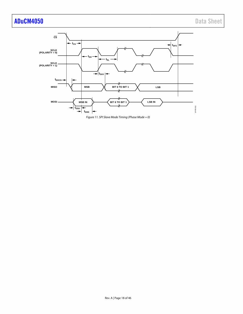
SPI SLAVE MODE TIMING Timing Requirements
CS to SCLK Edge tCS 38.5 ns SCLK Low Pulse Width tSL 38.5 ns SCLK High Pulse Width tSH 38.5 ns Data Input Setup Time Before SCLK Edge tDSU 6 ns Data Input Hold Time After SCLK Edge tDHD 8 ns
Switching Characteristics Data Output Valid After SCLK Edge tDAV 20 ns Data Output Valid After CS Edge tDOCS 20 ns CS High After SCLK Edge tSFS 38.5 ns
SPIH SLAVE MODE TIMING Timing Requirements
CS to SCLK Edge tCS 19.23 ns SCLK Low Pulse Width tSL 19.23 ns SCLK High Pulse Width tSH 19.23 ns Data Input Setup Time Before SCLK Edge tDSU 1 Data Input Hold Time After SCLK Edge tDHD 1
Switching Characteristics Data Output Valid After SCLK Edge tDAV 15 ns Data Output Valid After CS Edge tDOCS 15 ns CS High After SCLK Edge tSFS 19.23 ns
1 These specifications are characterized with respect to double drive strength.
Data Sheet ADuCM4050
Rev. A | Page 17 of 46
CS
MOSI MSB
MSB IN
BIT 6 TO BIT 1 LSB
LSB INBIT 6 TO BIT 1MISO
SCLK(POLARITY = 0)
SCLK(POLARITY = 1)
tCS tSFS
tSH
tDAV
tDSUtDHD
tSL
1474
5-00
8
Figure 8. SPI Master Mode Timing (Phase Mode = 1)
CS
MOSI MSB
MSB IN
BIT 6 TO BIT 1 LSB
LSB INBIT 6 TOBIT 1MISO
SCLK(POLARITY = 0)
SCLK(POLARITY = 1)
tCS tSFS
tSH
tDOSU
tDSUtDHD
tDAV
tSL
1474
5-00
9
Figure 9. SPI Master Mode Timing (Phase Mode = 0)
CS
MISO MSB
MSB IN
BIT 6 TO BIT 1 LSB
LSB INBIT 6 TO BIT 1MOSI
SCLK(POLARITY = 0)
SCLK(POLARITY = 1)
tCS tSFS
tSH
tDAV
tDSUtDHD
tSL
1474
5-01
0
Figure 10. SPI Slave Mode Timing (Phase Mode = 1)
ADuCM4050 Data Sheet
Rev. A | Page 18 of 46
CS
MISO MSB
MSB IN
BIT 6 TO BIT 1 LSB
LSB INBIT 6 TO BIT 1MOSI
SCLK(POLARITY = 0)
SCLK(POLARITY = 1)
tCS tSFS
tSH
tDAV
tDSUtDHD
tDOCS
tSL
1474
5-01
1
Figure 11. SPI Slave Mode Timing (Phase Mode = 0)

Data Sheet ADuCM4050
Rev. A | Page 19 of 46
I2C Specifications
Table 16. Parameter Symbol Min Typ Max Unit I2C SCLK FREQUENCY
Standard Mode 100 kHz Fast Mode 400 kHz
General-Purpose Port Timing
Table 17. Parameter Symbol Min Typ Max Unit TIMING REQUIREMENTS
General-Purpose Port Pin Input Pulse Width tWFI 4 × tPCLK ns
GPIO INPUT
tWFI
1474
5-01
2
Figure 12. General-Purpose Timing
RTC1 (FLEX_RTC) Specifications
Table 18. Parameter Symbol Min Typ Max Unit SensorStrobe
Minimum Output Frequency 0.5 Hz Maximum Output Frequency 16.384 kHz
RTC1 ALARM Minimum Time Resolution 30.52 µs
Timer Pulse-Width Modulation (PWM) Output Cycle Timing
Table 19. Parameter Symbol Min Typ Max Unit SWITCHING REQUIREMENTS
Timer Pulse Width Modulation Output tPWMO (4 × tPCLK) − 6 256 × (216 − 1) ns
PWM OUTPUTS
tPWMO14
745-
013
Figure 13. Timer PWM Output Cycle Timing
ADuCM4050 Data Sheet
Rev. A | Page 20 of 46
ABSOLUTE MAXIMUM RATINGS Table 20. Parameter Rating Supply
VBAT_ANA1, VBAT_ANA2, VBAT_ADC, VBAT_DIG1, VBAT_DIG2, and VREFP_ADC
−0.3 V to +3.6 V
Analog VDCDC_CAP1N, VDCDC_CAP1P,
VDCDC_OUT, VDCDC_CAP2N, and VDCDC_CAP2P
−0.3 V to +3.6 V
VLDO_OUT, SYS_HFXTAL_IN, SYS_HFXTAL_OUT, SYS_LFXTAL_IN, and SYS_LFXTAL_OUT
−0.3 V to +1.32 V
Digital Input/Output P0_xx, P1_xx, P2_xx, P3_xx, and
SYS_HWRST −0.3 V to +3.6 V
Stresses at or above those listed under Absolute Maximum Ratings may cause permanent damage to the product. This is a stress rating only; functional operation of the product at these or any other conditions above those indicated in the operational section of this specification is not implied. Operation beyond the maximum operating conditions for extended periods may affect product reliability.
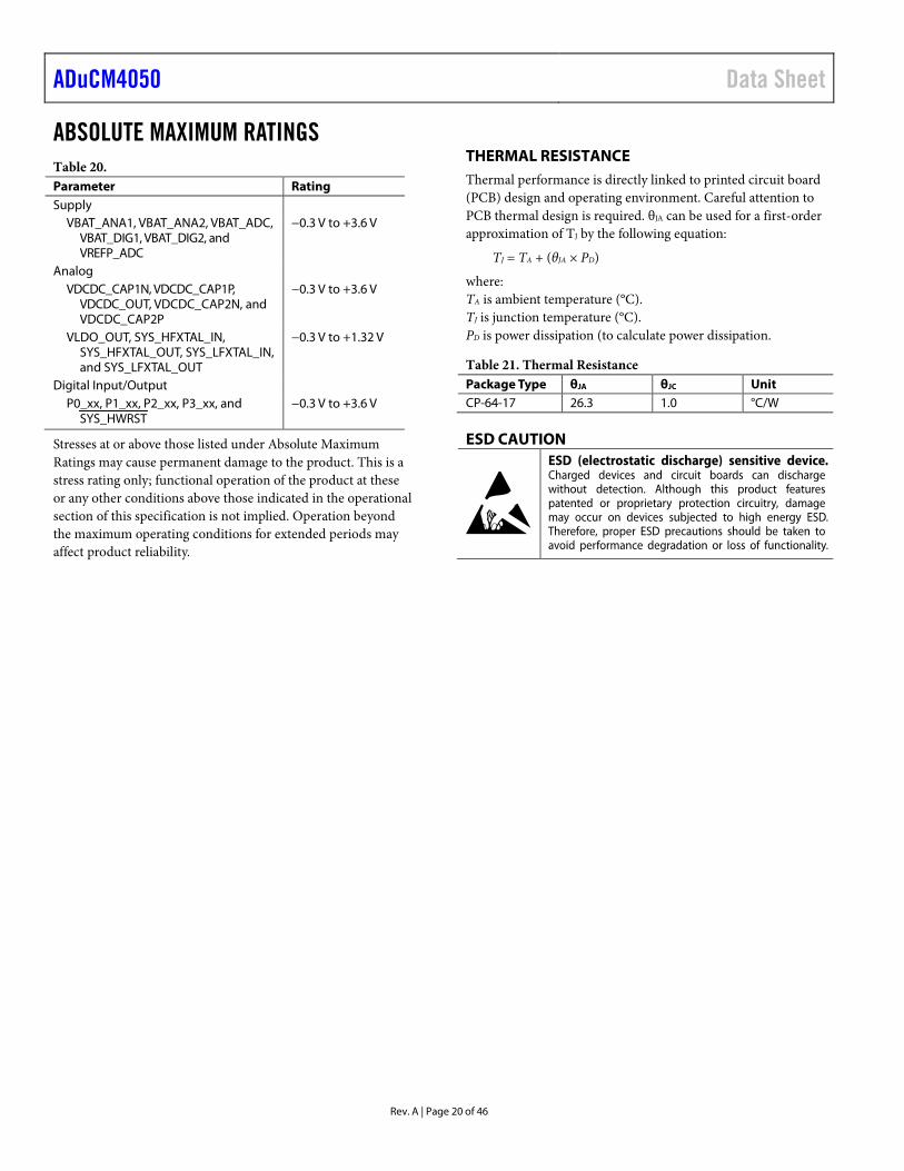
THERMAL RESISTANCE Thermal performance is directly linked to printed circuit board (PCB) design and operating environment. Careful attention to PCB thermal design is required. θJA can be used for a first-order approximation of TJ by the following equation:
TJ = TA + (θJA × PD)
where: TA is ambient temperature (°C). TJ is junction temperature (°C). PD is power dissipation (to calculate power dissipation.
Table 21. Thermal Resistance Package Type θJA θJC Unit CP-64-17 26.3 1.0 °C/W
ESD CAUTION
Data Sheet ADuCM4050
Rev. A | Page 21 of 46
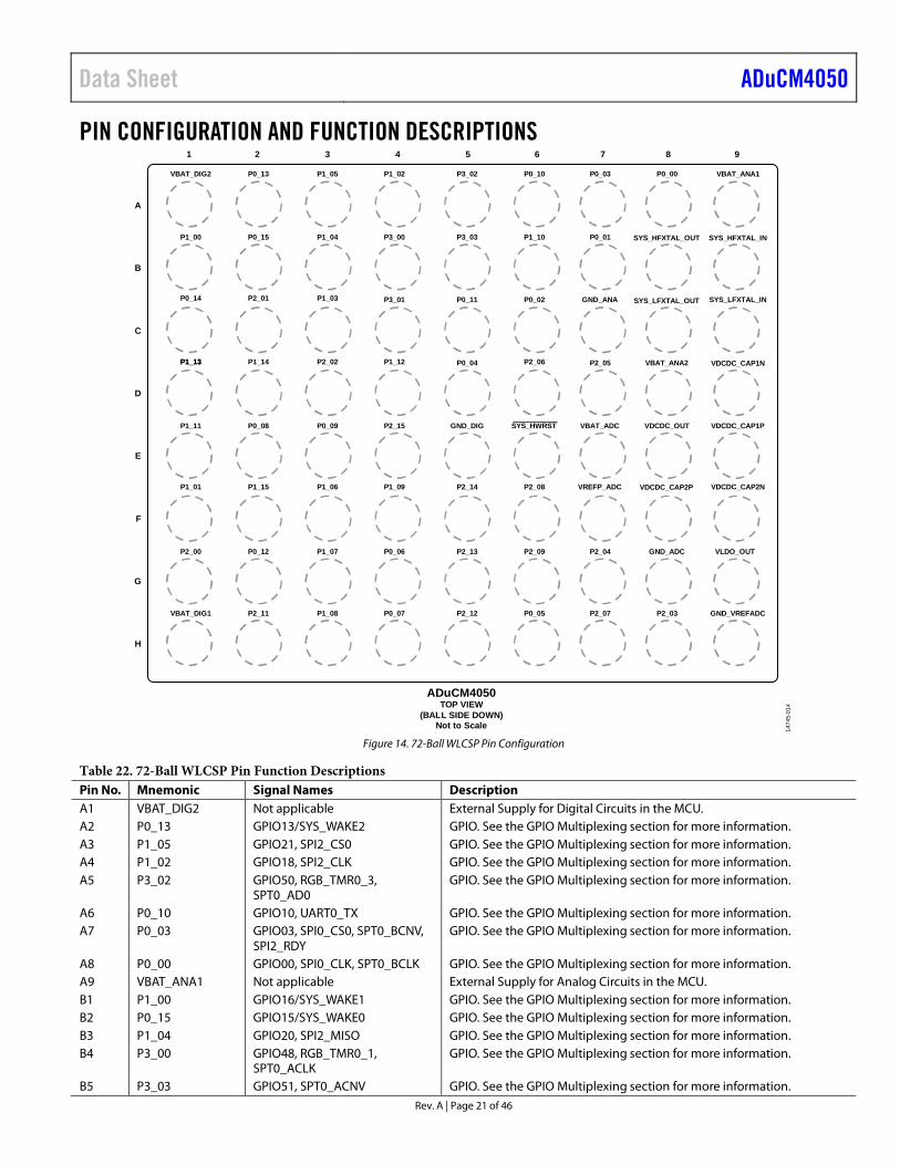
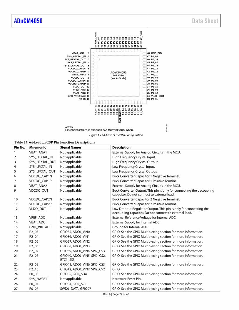
PIN CONFIGURATION AND FUNCTION DESCRIPTIONS
ADuCM4050TOP VIEW
(BALL SIDE DOWN)Not to Scale 14
745-
014
1
A
B
C
D
E
F
G
2 3 4 5 6 7 8
H
9
VBAT_DIG2 P0_13 P1_05 P1_02 P3_02 P0_10 P0_03 P0_00 VBAT_ANA1
P1_00 P0_15 P1_04 P3_00 P3_03 P1_10 P0_01 SYS_HFXTAL_OUT SYS_HFXTAL_IN
P0_14 P2_01 P1_03 P3_01 P0_11 P0_02 GND_ANA SYS_LFXTAL_OUT SYS_LFXTAL_IN
P1_13P1_13 P1_14 P2_02 P1_12 P0_04 P2_06 P2_05 VBAT_ANA2 VDCDC_CAP1N
P1_11 P0_08 P0_09 P2_15 GND_DIG SYS_HWRST VBAT_ADC VDCDC_OUT VDCDC_CAP1P
P1_01 P1_15 P1_06 P1_09 P2_14 VREFP_ADC VDCDC_CAP2PP2_08 VDCDC_CAP2N
P2_00 P0_12 P1_07 P0_06 P2_13 P2_09 P2_04 GND_ADC VLDO_OUT
P2_11 P1_08 P0_07 P2_12 P0_05 P2_07 P2_03 GND_VREFADCVBAT_DIG1
Figure 14. 72-Ball WLCSP Pin Configuration
Table 22. 72-Ball WLCSP Pin Function Descriptions Pin No. Mnemonic Signal Names Description A1 VBAT_DIG2 Not applicable External Supply for Digital Circuits in the MCU. A2 P0_13 GPIO13/SYS_WAKE2 GPIO. See the GPIO Multiplexing section for more information. A3 P1_05 GPIO21, SPI2_CS0 GPIO. See the GPIO Multiplexing section for more information. A4 P1_02 GPIO18, SPI2_CLK GPIO. See the GPIO Multiplexing section for more information. A5 P3_02 GPIO50, RGB_TMR0_3,
SPT0_AD0 GPIO. See the GPIO Multiplexing section for more information.
A6 P0_10 GPIO10, UART0_TX GPIO. See the GPIO Multiplexing section for more information. A7 P0_03 GPIO03, SPI0_CS0, SPT0_BCNV,
SPI2_RDY GPIO. See the GPIO Multiplexing section for more information.
A8 P0_00 GPIO00, SPI0_CLK, SPT0_BCLK GPIO. See the GPIO Multiplexing section for more information. A9 VBAT_ANA1 Not applicable External Supply for Analog Circuits in the MCU. B1 P1_00 GPIO16/SYS_WAKE1 GPIO. See the GPIO Multiplexing section for more information. B2 P0_15 GPIO15/SYS_WAKE0 GPIO. See the GPIO Multiplexing section for more information. B3 P1_04 GPIO20, SPI2_MISO GPIO. See the GPIO Multiplexing section for more information. B4 P3_00 GPIO48, RGB_TMR0_1,
SPT0_ACLK GPIO. See the GPIO Multiplexing section for more information.
B5 P3_03 GPIO51, SPT0_ACNV GPIO. See the GPIO Multiplexing section for more information.
ADuCM4050 Data Sheet
Rev. A | Page 22 of 46
Pin No. Mnemonic Signal Names Description B6 P1_10 GPIO26, SPI0_CS1, SYS_CLKIN,
SPI1_CS3 GPIO. See the GPIO Multiplexing section for more information.
B7 P0_01 GPIO01, SPI0_MOSI, SPT0_BFS GPIO. See the GPIO Multiplexing section for more information. B8 SYS_HFXTAL_OUT Not applicable High Frequency Crystal Output. B9 SYS_HFXTAL_IN Not applicable High Frequency Crystal Input. C1 P0_14 GPIO14, TMR0_OUT, SPI1_RDY GPIO. See the GPIO Multiplexing section for more information. C2 P2_01 GPIO33/SYS_WAKE3, TMR2_OUT GPIO. See the GPIO Multiplexing section for more information. C3 P1_03 GPIO19, SPI2_MOSI GPIO. See the GPIO Multiplexing section for more information. C4 P3_01 GPIO49, RGB_TMR0_2,
SPT0_AFS GPIO. See the GPIO Multiplexing section for more information.
C5 P0_11 GPIO11, UART0_RX GPIO. See the GPIO Multiplexing section for more information. C6 P0_02 GPIO02, SPI0_MISO, SPT0_BD0 GPIO. See the GPIO Multiplexing section for more information. C7 GND_ANA Not applicable Ground Reference for Analog Circuits in the MCU. C8 SYS_LFXTAL_OUT Not applicable Low Frequency Crystal Output. C9 SYS_LFXTAL_IN Not applicable Low Frequency Crystal Input. D1 P1_13 GPIO29, TMR2_OUT GPIO. See the GPIO Multiplexing section for more information. D2 P1_14 GPIO30, SPI0_RDY GPIO. See the GPIO Multiplexing section for more information. D3 P2_02 GPIO34, SPT0_ACNV, SPI1_CS2 GPIO. See the GPIO Multiplexing section for more information. D4 P1_12 GPIO28, RTC1_SS2 GPIO. See the GPIO Multiplexing section for more information. D5 P0_04 GPIO04, I2C0_SCL GPIO. See the GPIO Multiplexing section for more information. D6 P2_06 GPIO38, ADC0_VIN3 GPIO. See the GPIO Multiplexing section for more information. D7 P2_05 GPIO37, ADC0_VIN2 GPIO. See the GPIO Multiplexing section for more information. D8 VBAT_ANA2 Not applicable External Supply for Analog Circuits in the MCU. D9 VDCDC_CAP1N Not applicable Buck Converter Capacitor 1 Negative Terminal. E1 P1_11 GPIO27, TMR1_OUT GPIO. See the GPIO Multiplexing section for more information. E2 P0_08 GPIO08, BPR0_TONE_N GPIO. See the GPIO Multiplexing section for more information. E3 P0_09 GPIO09, BPR0_TONE_P,
SPI2_CS1 GPIO. See the GPIO Multiplexing section for more information.
E4 P2_15 GPIO47, SPI2_CS2, SPI1_CS3, SPI0_CS1
GPIO. See the GPIO Multiplexing section for more information.
E5 GND_DIG Not applicable Ground Reference for Digital Circuits in the MCU. E6 SYS_HWRST Not applicable Hardware Reset Pin.
E7 VBAT_ADC Not applicable External Supply for Internal ADC. E8 VDCDC_OUT Not applicable Buck Converter Output. This pin is only for connecting the decoupling
capacitor. Do not connect to external load. E9 VDCDC_CAP1P Not applicable Buck Converter Capacitor 1 Positive Terminal. F1 P1_01 SYS_BMODE0, GPIO17 GPIO. See the GPIO Multiplexing section for more information. F2 P1_15 GPIO31, SPT0_ACLK, UART1_TX GPIO. See the GPIO Multiplexing section for more information. F3 P1_06 GPIO22, SPI1_CLK, RGB_TMR0_1 GPIO. See the GPIO Multiplexing section for more information. F4 P1_09 GPIO25, SPI1_CS0, SWV GPIO. See the GPIO Multiplexing section for more information. F5 P2_14 GPIO46, SPI0_CS3 GPIO. See the GPIO Multiplexing section for more information. F6 P2_08 GPIO40, ADC0_VIN5, SPI0_CS2,
RTC1_SS3 GPIO. See the GPIO Multiplexing section for more information.
F7 VREFP_ADC Not applicable External Reference Voltage for Internal ADC. F8 VDCDC_CAP2P Not applicable Buck Converter Capacitor 2 Positive Terminal. F9 VDCDC_CAP2N Not applicable Buck Converter Capacitor 2 Negative Terminal. G1 P2_00 GPIO32, SPT0_AFS, UART1_RX GPIO. See the GPIO Multiplexing section for more information. G2 P0_12 GPIO12, SPT0_AD0,
UART0_SOUT_EN GPIO. See the GPIO Multiplexing section for more information.
G3 P1_07 GPIO23, SPI1_MOSI, RGB_TMR0_2
GPIO. See the GPIO Multiplexing section for more information.
G4 P0_06 SWD0_CLK, GPIO06 GPIO. See the GPIO Multiplexing section for more information. G5 P2_13 GPIO45, UART1_RX, SPI0_CS2 GPIO. See the GPIO Multiplexing section for more information. G6 P2_09 GPIO41, ADC0_VIN6, SPI0_CS3 GPIO. See the GPIO Multiplexing section for more information.
Data Sheet ADuCM4050
Rev. A | Page 23 of 46
Pin No. Mnemonic Signal Names Description G7 P2_04 GPIO36, ADC0_VIN1 GPIO. See the GPIO Multiplexing section for more information. G8 GND_ADC Not applicable Ground Pin for Internal ADC. G9 VLDO_OUT Not applicable Low Drop Out Regulator Output. This pin is only for connecting the
decoupling capacitor. Do not connect to external load. H1 VBAT_DIG1 Not applicable External Supply for Digital Circuits in the MCU. H2 P2_11 GPIO43, SPI1_CS1, SYS_CLKOUT,
RTC1_SS1 GPIO. See the GPIO Multiplexing section for more information.
H3 P1_08 GPIO24, SPI1_MISO, RGB_TMR0_3
GPIO. See the GPIO Multiplexing section for more information.
H4 P0_07 SWD0_DATA, GPIO07 GPIO. See the GPIO Multiplexing section for more information. H5 P2_12 GPIO44, UART1_TX, SPI2_CS3 GPIO. See the GPIO Multiplexing section for more information. H6 P0_05 GPIO05, I2C0_SDA GPIO. See the GPIO Multiplexing section for more information. H7 P2_07 GPIO39, ADC0_VIN4, SPI2_CS3 GPIO. See the GPIO Multiplexing section for more information. H8 P2_03 GPIO35, ADC0_VIN0 GPIO. See the GPIO Multiplexing section for more information. H9 GND_VREFADC Not applicable Ground for ADC Reference Supply.
ADuCM4050 Data Sheet
Rev. A | Page 24 of 46
1474
5-01
5
ADuCM4050TOP VIEW
(Not to Scale)
17 18 19 20 21 22 23 24 25 26 27 28 29 30 31 32
P2_0
4P2
_05
P2_0
6P2
_07
P2_0
8P2
_09
P2_1
0P0
_05
SYS_
HWRS
TP0
_04
P0_0
7P0
_06
P0_0
9P1
_08
P1_0
7P1
_06
64 63 62 61 60 59 58 57 56 55 54 53 52 51 50 49
GND
_AN
AP0
_00
P0_0
1P0
_02
P0_0
3P1
_10
P0_1
0P0
_11
P1_0
2P1
_03
P1_0
4P1
_05
P2_0
1P0
_13
P0_1
5VB
AT_D
IG2
123456789
10111213141516
VBAT_ANA1SYS_HFXTAL_IN
SYS_HFXTAL_OUT
NOTES1. EXPOSED PAD. THE EXPOSED PAD MUST BE GROUNDED.
SYS_LFXTAL_INSYS_LFXTAL_OUT
VDCDC_CAP1NVDCDC_CAP1P
VBAT_ANA2VDCDC_OUT
VDCDC_CAP2NVDCDC_CAP2P
VLDO_OUTVREF_ADCVBAT_ADC
GND_VREFDACP2_03
GND_DIGP1_00P0_14P2_02P1_14P1_13P1_12P1_11P0_08P0_09P1_01P1_15P2_00P0_12VBAT_DIG1P2_11
48474645444342414039383736353433
Figure 15. 64-Lead LFCSP Pin Configuration
Table 23. 64-Lead LFCSP Pin Function Descriptions Pin No. Mnemonic Signal Names Description 1 VBAT_ANA1 Not applicable External Supply for Analog Circuits in the MCU. 2 SYS_HFXTAL_IN Not applicable High Frequency Crystal Input. 3 SYS_HFXTAL_OUT Not applicable High Frequency Crystal Output. 4 SYS_LFXTAL_IN Not applicable Low Frequency Crystal Input. 5 SYS_LFXTAL_OUT Not applicable Low Frequency Crystal Output. 6 VDCDC_CAP1N Not applicable Buck Converter Capacitor 1 Negative Terminal. 7 VDCDC_CAP1P Not applicable Buck Converter Capacitor 1 Positive Terminal. 8 VBAT_ANA2 Not applicable External Supply for Analog Circuits in the MCU. 9 VDCDC_OUT Not applicable Buck Converter Output. This pin is only for connecting the decoupling
capacitor. Do not connect to external load. 10 VDCDC_CAP2N Not applicable Buck Converter Capacitor 2 Negative Terminal. 11 VDCDC_CAP2P Not applicable Buck Converter Capacitor 2 Positive Terminal. 12 VLDO_OUT Not applicable Low Dropout Regulator Output. This pin is only for connecting the
decoupling capacitor. Do not connect to external load. 13 VREF_ADC Not applicable External Reference Voltage for Internal ADC. 14 VBAT_ADC Not applicable External Supply for Internal ADC. 15 GND_VREFADC Not applicable Ground for Internal ADC. 16 P2_03 GPIO35, ADC0_VIN0 GPIO. See the GPIO Multiplexing section for more information. 17 P2_04 GPIO36, ADC0_VIN1 GPIO. See the GPIO Multiplexing section for more information. 18 P2_05 GPIO37, ADC0_VIN2 GPIO. See the GPIO Multiplexing section for more information. 19 P2_06 GPIO38, ADC0_VIN3 GPIO. See the GPIO Multiplexing section for more information. 20 P2_07 GPIO39, ADC0_VIN4, SPI2_CS3 GPIO. See the GPIO Multiplexing section for more information. 21 P2_08 GPIO40, ADC0_VIN5, SPI0_CS2,
RTC1_SS3 GPIO. See the GPIO Multiplexing section for more information.
22 P2_09 GPIO41, ADC0_VIN6, SPI0_CS3 GPIO. See the GPIO Multiplexing section for more information. 23 P2_10 GPIO42, ADC0_VIN7, SPI2_CS2 GPIO. 24 P0_05 GPIO05, I2C0_SDA GPIO. See the GPIO Multiplexing section for more information. 25 SYS_HWRST Not applicable Hardware Reset Pin.
26 P0_04 GPIO04, I2C0_SCL GPIO. See the GPIO Multiplexing section for more information. 27 P0_07 SWD0_DATA, GPIO07 GPIO. See the GPIO Multiplexing section for more information.
Data Sheet ADuCM4050
Rev. A | Page 25 of 46
Pin No. Mnemonic Signal Names Description 28 P0_06 SWD0_CLK, GPIO06 GPIO. See the GPIO Multiplexing section for more information. 29 P1_09 GPIO25, SPI1_CS0, SWV GPIO. See the GPIO Multiplexing section for more information. 30 P1_08 GPIO24, SPI1_MISO,
RGB_TMR0_3 GPIO. See the GPIO Multiplexing section for more information.
31 P1_07 GPIO23, SPI1_MOSI, RGB_TMR0_2
GPIO. See the GPIO Multiplexing section for more information.
32 P1_06 GPIO22, SPI1_CLK, RGB_TMR0_1 GPIO. See the GPIO Multiplexing section for more information. 33 P2_11 GPIO43, SPI1_CS1, SYS_CLKOUT,
RTC1_SS1 GPIO. See the GPIO Multiplexing section for more information.
34 VBAT_DIG1 Not applicable External Supply for Digital Circuits in the MCU. 35 P0_12 GPIO12, SPT0_AD0,
UART0_SOUT_EN GPIO. See the GPIO Multiplexing section for more information.
36 P2_00 GPIO32, SPT0_AFS, UART1_RX GPIO. See the GPIO Multiplexing section for more information. 37 P1_15 GPIO31, SPT0_ACLK, UART1_TX GPIO. See the GPIO Multiplexing section for more information. 38 P1_01 SYS_BMODE0, GPIO17 GPIO. See the GPIO Multiplexing section for more information. 39 P0_09 GPIO09, BPR0_TONE_P,
SPI2_CS1 GPIO. See the GPIO Multiplexing section for more information.
40 P0_08 GPIO08, BPR0_TONE_N GPIO. See the GPIO Multiplexing section for more information. 41 P1_11 GPIO27, TMR1_OUT GPIO. See the GPIO Multiplexing section for more information. 42 P1_12 GPIO28, RTC1_SS2 GPIO. See the GPIO Multiplexing section for more information. 43 P1_13 GPIO29, TMR2_OUT GPIO. See the GPIO Multiplexing section for more information. 44 P1_14 GPIO30, SPI0_RDY GPIO. See the GPIO Multiplexing section for more information. 45 P2_02 GPIO34, SPT0_ACNV, SPI1_CS2 GPIO. See the GPIO Multiplexing section for more information. 46 P0_14 GPIO14, TMR0_OUT, SPI1_RDY GPIO. See the GPIO Multiplexing section for more information. 47 P1_00 GPIO16/SYS_WAKE1 GPIO. See the GPIO Multiplexing section for more information. 48 GND_DIG Not applicable Ground Reference for Digital Circuits in the MCU. 49 VBAT_DIG2 Not applicable External Supply for Digital Circuits in the MCU. 50 P0_15 GPIO15/SYS_WAKE0 GPIO. See the GPIO Multiplexing section for more information. 51 P0_13 GPIO13/SYS_WAKE2 GPIO. See the GPIO Multiplexing section for more information. 52 P2_01 GPIO33/SYS_WAKE3, TMR2_OUT GPIO. See the GPIO Multiplexing section for more information. 53 P1_05 GPIO21, SPI2_CS0 GPIO. See the GPIO Multiplexing section for more information. 54 P1_04 GPIO20, SPI2_MISO GPIO. See the GPIO Multiplexing section for more information. 55 P1_03 GPIO19, SPI2_MOSI GPIO. See the GPIO Multiplexing section for more information. 56 P1_02 GPIO18, SPI2_CLK GPIO. See the GPIO Multiplexing section for more information. 57 P0_11 GPIO11, UART0_RX GPIO. See the GPIO Multiplexing section for more information.
58 P0_10 GPIO10, UART0_TX GPIO. See the GPIO Multiplexing section for more information.
59 P1_10 GPIO26, SPI0_CS1, SYS_CLKIN, SPI1_CS3
GPIO. See the GPIO Multiplexing section for more information.
60 P0_03 GPIO03, SPI0_CS0, SPT0_BCNV, SPI2_RDY
GPIO. See the GPIO Multiplexing section for more information.
61 P0_02 GPIO02, SPI0_MISO, SPT0_BD0 GPIO. See the GPIO Multiplexing section for more information. 62 P0_01 GPIO01, SPI0_MOSI, SPT0_BFS GPIO. See the GPIO Multiplexing section for more information. 63 P0_00 GPIO00, SPI0_CLK, SPT0_BCLK GPIO. See the GPIO Multiplexing section for more information. 64 GND_ANA Not applicable Ground Reference for Analog Circuits in the MCU. EPAD Not applicable Exposed Pad. The exposed pad must be grounded.
ADuCM4050 Data Sheet
Rev. A | Page 26 of 46
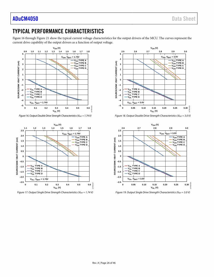
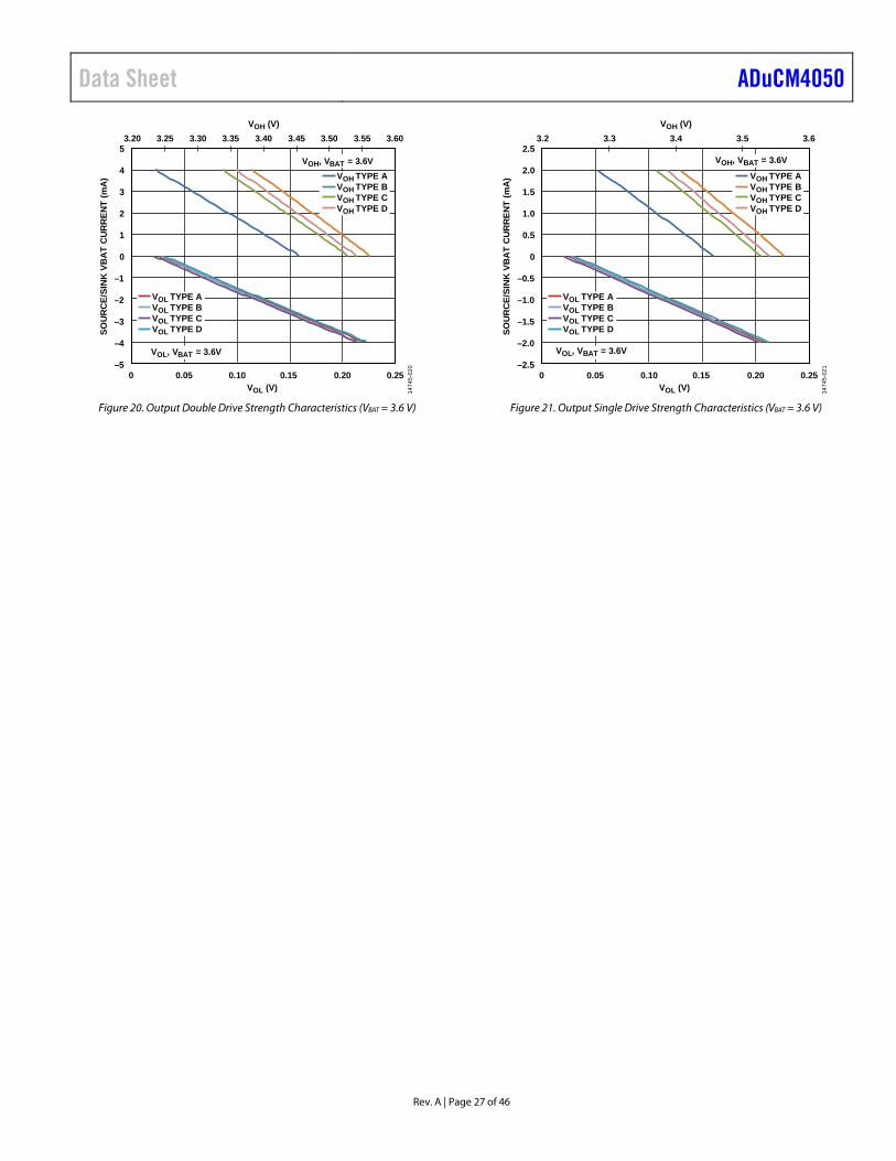
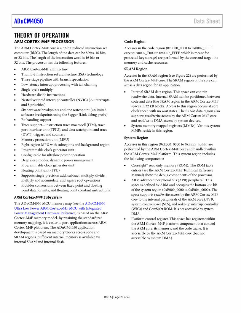
TYPICAL PERFORMANCE CHARACTERISTICS Figure 16 through Figure 21 show the typical current voltage characteristics for the output drivers of the MCU. The curves represent the current drive capability of the output drivers as a function of output voltage.
0.9 1.0 1.2 1.4 1.61.1 1.3 1.5 1.7 1.8
–5
–4
–3
–2
–1
0
1
2
3
4
5
0 0.1 0.2 0.3 0.4 0.5 0.6
VOH (V)
SOU
RC
E/SI
NK
VB
AT
CU
RR
ENT
(mA
)
VOL (V)
VOH, VBAT = 1.74V
VOL, VBAT = 1.74V
1474
5-01
6
VOH TYPE AVOH TYPE BVOH TYPE CVOH TYPE D
VOL TYPE AVOL TYPE BVOL TYPE CVOL TYPE D
Figure 16. Output Double Drive Strength Characteristics (VBAT = 1.74 V)
1.1 1.2 1.3 1.4 1.5 1.6 1.7 1.8
–2.5
–2.0
–1.5
–1.0
–0.5
0
0.5
1.0
1.5
2.0
2.5
0 0.1 0.2 0.3 0.4 0.5 0.6
SOUR
CE/S
INK
VBAT
CUR
RENT
(mA)
1474
5-01
7
VOH (V)
VOL (V)
VOH, VBAT = 1.74V
VOL, VBAT = 1.74V
VOH TYPE AVOH TYPE BVOH TYPE CVOH TYPE D
VOL TYPE AVOL TYPE BVOL TYPE CVOL TYPE D
Figure 17. Output Single Drive Strength Characteristics (VBAT = 1.74 V)
2.5 2.6 2.7 2.8 2.9 3.0
–5
–4
–3
–2
–1
0
1
2
3
4
5
0 0.05 0.10 0.15 0.20 0.25 0.30
SOU
RC
E/SI
NK
VB
AT
CU
RR
ENT
(mA
)
1474
5-01
8
VOH (V)
VOL (V)
VOH, VBAT = 3.0V
VOL, VBAT = 3.0V
VOH TYPE AVOH TYPE BVOH TYPE CVOH TYPE D
VOL TYPE AVOL TYPE BVOL TYPE CVOL TYPE D
Figure 18. Output Double Drive Strength Characteristics (VBAT = 3.0 V)
2.6 2.7 2.8 2.9 3.0
0 0.05 0.10 0.15 0.20 0.25 0.30
SOUR
CE/S
INK
VBAT
CUR
RENT
(mA)
1474
5-01
9–2.5
–2.0
–1.5
–1.0
–0.5
0.5
0
1.0
1.5
2.0
2.5
VOH (V)
VOL (V)
VOH, VBAT = 3.0V
VOL, VBAT = 3.0V
VOH TYPE AVOH TYPE BVOH TYPE CVOH TYPE D
VOL TYPE AVOL TYPE BVOL TYPE CVOL TYPE D
Figure 19. Output Single Drive Strength Characteristics (VBAT = 3.0 V)
Data Sheet ADuCM4050
Rev. A | Page 27 of 46
3.20 3.30 3.40 3.503.25 3.35 3.45 3.55 3.60
–5
–4
–3
–2
–1
0
1
2
3
4
5
0 0.05 0.10 0.15 0.20 0.25
SOU
RC
E/SI
NK
VB
AT
CU
RR
ENT
(mA
)
1474
5-02
0
VOH (V)
VOL (V)
VOH, VBAT = 3.6V
VOL, VBAT = 3.6V
VOH TYPE AVOH TYPE BVOH TYPE CVOH TYPE D
VOL TYPE AVOL TYPE BVOL TYPE CVOL TYPE D
Figure 20. Output Double Drive Strength Characteristics (VBAT = 3.6 V)
3.2 3.3 3.4 3.5 3.6
0 0.05 0.10 0.15 0.20 0.25
SOUR
CE/S
INK
VBAT
CUR
RENT
(mA)
1474
5-02
1–2.5
–2.0
–1.5
–1.0
–0.5
0
0.5
1.0
1.5
2.0
2.5
VOH (V)
VOL (V)
VOH, VBAT = 3.6V
VOL, VBAT = 3.6V
VOH TYPE AVOH TYPE BVOH TYPE CVOH TYPE D
VOL TYPE AVOL TYPE BVOL TYPE CVOL TYPE D
Figure 21. Output Single Drive Strength Characteristics (VBAT = 3.6 V)
ADuCM4050 Data Sheet
Rev. A | Page 28 of 46
THEORY OF OPERATION ARM CORTEX-M4F PROCESSOR The ARM Cortex-M4F core is a 32-bit reduced instruction set computer (RISC). The length of the data can be 8 bits, 16 bits, or 32 bits. The length of the instruction word is 16 bits or 32 bits. The processor has the following features:
• ARM Cortex-M4F architecture • Thumb-2 instruction set architecture (ISA) technology • Three-stage pipeline with branch speculation • Low latency interrupt processing with tail chaining • Single-cycle multiply • Hardware divide instructions • Nested vectored interrupt controller (NVIC) (72 interrupts
and 8 priorities) • Six hardware breakpoints and one watchpoint (unlimited
software breakpoints using the Segger JLink debug probe) • Bit banding support • Trace support—instruction trace macrocell (ITM), trace
port interface unit (TPIU), and data watchpoint and trace (DWT) triggers and counters
• Memory protection unit (MPU) • Eight-region MPU with subregions and background region • Programmable clock generator unit • Configurable for ultralow power operation • Deep sleep modes, dynamic power management • Programmable clock generator unit • Floating point unit (FPU) • Supports single-precision add, subtract, multiply, divide,
multiply and accumulate, and square root operations • Provides conversions between fixed point and floating
point data formats, and floating point constant instructions
ARM Cortex-M4F Subsystem
The ADuCM4050 MCU memory map (see the ADuCM4050 Ultra Low Power ARM Cortex-M4F MCU with Integrated Power Management Hardware Reference) is based on the ARM Cortex-M4F memory model. By retaining the standardized memory mapping, it is easier to port applications across ARM Cortex-M4F platforms. The ADuCM4050 application development is based on memory blocks across code and SRAM regions. Sufficient internal memory is available via internal SRAM and internal flash.
Code Region
Accesses in the code region (0x0000_0000 to 0x0007_FFFF except 0x0007_F000 to 0x0007_FFFF, which is meant for protected key storage) are performed by the core and target the memory and cache resources.
SRAM Region
Accesses in the SRAM region (see Figure 22) are performed by the ARM Cortex-M4F core. The SRAM region of the core can act as a data region for an application.
• Internal SRAM data region. This space can contain read/write data. Internal SRAM can be partitioned between code and data (the SRAM region in the ARM Cortex-M4F space) in 32 kB blocks. Access to this region occurs at core clock speed with no wait states. The SRAM data region also supports read/write access by the ARM Cortex-M4F core and read/write DMA access by system devices.
• System memory mapped registers (MMRs). Various system MMRs reside in this region.
System Region
Accesses in this region (0xE000_0000 to 0xFFFF_FFFF) are performed by the ARM Cortex-M4F core and handled within the ARM Cortex-M4F platform. This system region includes the following components:
• CoreSight™ read only memory (ROM). The ROM table entries (see the ARM Cortex-M4F Technical Reference Manual) show the debug components of the processor.
• ARM advanced peripheral bus (APB) peripheral. This space is defined by ARM and occupies the bottom 256 kB of the system region (0xE000_0000 to 0xE004_0000). The space supports read/write access by the ARM Cortex-M4F core to the internal peripherals of the ARM core (NVIC, system control space (SCS), and wake-up interrupt controller (WIC)) and CoreSight ROM. It is not accessible by system DMA.
• Platform control register. This space has registers within the ARM Cortex-M4F platform component that control the ARM core, its memory, and the code cache. It is accessible by the ARM Cortex-M4F core (but not accessible by system DMA).
Data Sheet ADuCM4050
Rev. A | Page 29 of 46
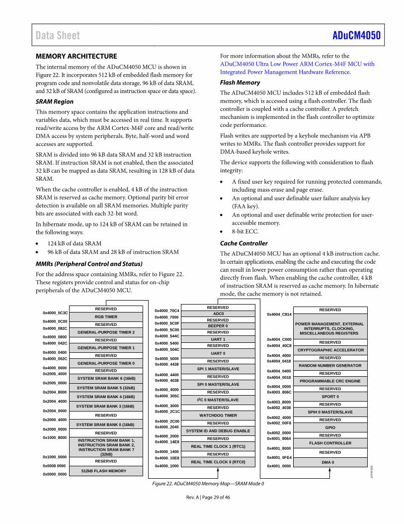
MEMORY ARCHITECTURE The internal memory of the ADuCM4050 MCU is shown in Figure 22. It incorporates 512 kB of embedded flash memory for program code and nonvolatile data storage, 96 kB of data SRAM, and 32 kB of SRAM (configured as instruction space or data space).
SRAM Region
This memory space contains the application instructions and variables data, which must be accessed in real time. It supports read/write access by the ARM Cortex-M4F core and read/write DMA access by system peripherals. Byte, half-word and word accesses are supported.
SRAM is divided into 96 kB data SRAM and 32 kB instruction SRAM. If instruction SRAM is not enabled, then the associated 32 kB can be mapped as data SRAM, resulting in 128 kB of data SRAM.
When the cache controller is enabled, 4 kB of the instruction SRAM is reserved as cache memory. Optional parity bit error detection is available on all SRAM memories. Multiple parity bits are associated with each 32-bit word.
In hibernate mode, up to 124 kB of SRAM can be retained in the following ways:
• 124 kB of data SRAM • 96 kB of data SRAM and 28 kB of instruction SRAM
MMRs (Peripheral Control and Status)
For the address space containing MMRs, refer to Figure 22. These registers provide control and status for on-chip peripherals of the ADuCM4050 MCU.
For more information about the MMRs, refer to the ADuCM4050 Ultra Low Power ARM Cortex-M4F MCU with Integrated Power Management Hardware Reference.
Flash Memory
The ADuCM4050 MCU includes 512 kB of embedded flash memory, which is accessed using a flash controller. The flash controller is coupled with a cache controller. A prefetch mechanism is implemented in the flash controller to optimize code performance.
Flash writes are supported by a keyhole mechanism via APB writes to MMRs. The flash controller provides support for DMA-based keyhole writes.
The device supports the following with consideration to flash integrity:
• A fixed user key required for running protected commands, including mass erase and page erase.
• An optional and user definable user failure analysis key (FAA key).
• An optional and user definable write protection for user-accessible memory.
• 8-bit ECC.
Cache Controller
The ADuCM4050 MCU has an optional 4 kB instruction cache. In certain applications, enabling the cache and executing the code can result in lower power consumption rather than operating directly from flash. When enabling the cache controller, 4 kB of instruction SRAM is reserved as cache memory. In hibernate mode, the cache memory is not retained.
0x0000_0000
0x0008 0000512kB FLASH MEMORY
0x1000_0000
0x1000_8000 INSTRUCTION SRAM BANK 1,INSTRUCTION SRAM BANK 2,INSTRUCTION SRAM BANK 7
(32kB)
0x2000_0000SYSTEM SRAM BANK 0 (16kB)
0x2000_4000
0x2004_0000SYSTEM SRAM BANK 3 (16kB)
0x2004_4000
0x2004_8000SYSTEM SRAM BANK 4 (16kB)
RESERVED
RESERVED
RESERVED
0x4000_0000
0x4000_002CRESERVED
RESERVED
RESERVED
RESERVED
GENERAL-PURPOSE TIMER 0
0x4000_0400
0x4000_042CGENERAL-PURPOSE TIMER 1
0x4000_0800
0x4000_082CGENERAL-PURPOSE TIMER 2
0x4000_0C00
0x4000_0C3CRGB TIMER
SYSTEM SRAM BANK 5 (32kB)0x2005_0000
0x2005_4000SYSTEM SRAM BANK 6 (16kB)
RESERVED
RESERVED
0x4000_1000
0x4000_10E8REAL TIME CLOCK 0 (RTC0)
RESERVED
RESERVED
RESERVED
RESERVED
RESERVED
RESERVED
RESERVED
0x4000_1400
0x4000_14E8REAL TIME CLOCK 1 (RTC1)
0x4000_2000
0x4000_2040SYSTEM ID AND DEBUG ENABLE
0x4000_2C00
0x4000_2C1CWATCHDOG TIMER
0x4000_3000
0x4000_305CI2C 0 MASTER/SLAVE
0x4000_4000
0x4000_4038SPI 0 MASTER/SLAVE
0x4000_4400
0x4000_4438SPI 1 MASTER/SLAVE
0x4000_5000
0x4000_504CUART 0
RESERVED
RESERVED
0x4001_8000
0x4001_8064FLASH CONTROLLER
0x4002_0000
0x4002_00F8GPIO
RESERVED
RESERVED
RESERVED
RESERVED
RESERVED
RESERVED
0x4002_4000
0x4002_4038SPIH 0 MASTER/SLAVE
0x4003_8000
0x4003_806CSPORT 0
0x4004_0000
0x4004_0018PROGRAMMABLE CRC ENGINE
0x4004_0400
0x4004_0418RANDOM NUMBER GENERATOR
0x4004_4000
0x4004_40C8CRYPTOGRAPHIC ACCELERATOR
0x4004_C000
0x4004_C814
POWER MANAGEMENT, EXTERNALINTERRUPTS, CLOCKING,
MISCELLANEOUS REGISTERS
RESERVED
0x4000_5C000x4000_5C0F BEEPER 0
RESERVED
0x4000_5400
0x4000_544CUART 1
0x4001_0000
0x4001_0FE4DMA 0
RESERVED
RESERVED
0x4000_70000x4000_70C4
ADC0
1474
5-02
2
Figure 22. ADuCM4050 Memory Map—SRAM Mode 0
ADuCM4050 Data Sheet
Rev. A | Page 30 of 46
SYSTEM INTEGRATION FEATURES The ADuCM4050 MCU provides several features for development of ultra low power, secure, and robust systems.
Reset
There are four kinds of resets: external, power-on, watchdog timeout, and software system reset. The software system reset is provided as part of the ARM Cortex-M4F core. The SYS_HWRST pin is toggled to perform a hardware reset.
Booting
The ADuCM4050 MCU supports two boot modes: booting from internal flash and upgrading software through UART download (see Table 24). If SYS_BMODE0 (Pin P1_01) is pulled low during power-up or a hard reset, the MCU enters into serial download mode. In this mode, an on-chip loader routine initiates in the kernel, which configures the UART port and communicates with the host to manage the firmware upgrade via a specific serial download protocol.
Table 24. Boot Modes Boot Mode Description 0 UART download mode. 1 Flash boot. Boot from integrated flash memory.
Power Management and Modes
The ADuCM4050 MCU has an integrated power management system that optimizes performance and extends the battery life of the device. The power management system consists of the following:
• Integrated 1.2 V low dropout regulator (LDO) and optional capacitive buck regulator
• Integrated power switches for low standby current in hibernate and shutdown modes
Additional power management features include the following:
• Customized clock gating for active modes • Power gating to reduce leakage in hibernate and shutdown
modes • Flexible sleep modes • Shutdown mode with no retention • Optional high efficiency buck converter to reduce power • Integrated low power oscillators
The PMU provides control of the ADuCM4050 MCU power modes and allows the ARM Cortex-M4F to control the clocks and power gating to reduce the power consumption. Several power modes are available, offering options to balance power consumption and functionality. The power modes available in the ADuCM4050 are described in the following sections.
Active Mode
In active mode, all peripherals can be enabled. Active power is managed by optimized clock management. See Table 3 for details on active mode current consumption.
Flexi Mode
In flexi mode, the ARM Cortex-M4F core is clock gated, but the remainder of the system is active. No instructions can be executed in this mode, but DMA transfers can continue between peripherals as well as memory to memory. See Table 4 for details on flexi mode current consumption.
Hibernate Mode
Hibernate mode provides state retention, configurable SRAM and port pin retention, a limited number of wake-up interrupts (SYS_WAKEx, UART0_RX, and optionally, RTC0 and RTC1 (FLEX_RTC™)).
Shutdown Mode
Shutdown mode is the deepest sleep mode, in which all the digital and analog circuits are powered down with an option to wake from four possible wake-up sources. The RTC0 can be (optionally) enabled in this mode, and the device can be periodically woken up by the RTC0 interrupt.
Shutdown Mode—Fast Wake-Up
This mode has a faster wake-up time than shutdown mode at the expense of higher power consumption. See Table 25 for wake-up time specifications.
Power Management and Control
The following features are available for power management and control:
• Voltage range of 1.74 V to 3.6 V using a single supply (such as the CR2032 coin cell battery).
• GPIOs are driven directly from the battery. The pin state is retained in hibernate and shutdown modes. The GPIO configuration is only retained in hibernate mode.
• Wake-up from external interrupts (via GPIOs), UART0_RX interrupt, and RTCs for hibernate mode.
• Wake-up from external interrupts (via GPIOs) and RTC0 for shutdown mode.
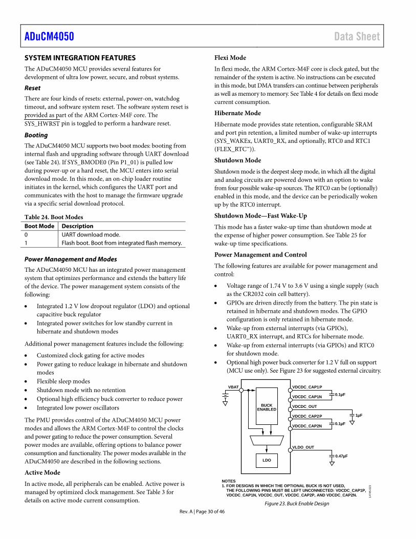
• Optional high power buck converter for 1.2 V full on support (MCU use only). See Figure 23 for suggested external circuitry.
BUCKENABLED
LDO
NOTES1. FOR DESIGNS IN WHICH THE OPTIONAL BUCK IS NOT USED, THE FOLLOWING PINS MUST BE LEFT UNCONNECTED: VDCDC_CAP1P, VDCDC_CAP1N, VDCDC_OUT, VDCDC_CAP2P, AND VDCDC_CAP2N.
VDCDC_CAP1PVBAT
0.1µF
1µF
0.1µF
VDCDC_CAP1N
VDCDC_OUT
VDCDC_CAP2P
0.47µF
VLDO_OUT
VDCDC_CAP2N
1474
5-02
3
Figure 23. Buck Enable Design
Data Sheet ADuCM4050
Rev. A | Page 31 of 46
Table 25. Power Modes Wake-Up Times Mode VTOR1 Root Clock HCLK/PCLK Wake-Up Time Flexi Flash HFOSC 26 MHz 1.605 µs Hibernate Flash HFOSC 26 MHz 10.356 µs SRAM HFOSC 26 MHz 4.984 µs Flash HFXTAL 26 MHz 686.452 µs Flash PLL_HFOSC 26 MHz 14.487 µs Flash PLL_HFXTAL 26 MHz 742.668 µs Flash PLL_HFOSC 52 MHz 15.730 µs Flash PLL_HFXTAL 52 MHz 726.101 µs Shutdown Flash HFOSC 26 MHz 68.144 ms Shutdown (Fast Wake-Up) Flash HFOSC 26 MHz 1.220 ms 1 VTOR means vector table offset register.
Security Features
The ADuCM4050 MCU provides a combination of hardware and software protection mechanisms that lock out access to the device in secure mode, but grant access in open mode. These mechanisms include the password protected slave boot mode (UART), as well as password protected serial wire debug (SWD) interfaces. Mechanisms are provided to protect the device contents (flash, SRAM, CPU registers, and peripheral registers) from being read through an external interface by an unauthorized user. This is referred to as read protection.
It is possible to protect the device from being reprogrammed in circuit with unauthorized code. This is referred to as in circuit write protection.
The device can be configured with no protection, read protection, or read and in circuit write protection. It is not necessary to provide in circuit write protection without read protection.
This product includes security features that can be used to protect embedded nonvolatile memory contents and prevent execution of unauthorized code. When security is enabled on this device (either by the ordering party or the subsequent receiving parties), the ability of Analog Devices to conduct failure analysis on returned devices is limited. Contact Analog Devices for details on the failure analysis limitations for this device.
Cryptographic Accelerator
The cryptographic accelerator is a 32-bit APB DMA capable peripheral. There are two 128-bit buffers provided for data input/output operations. These buffers read in or read out 128 bits in four data accesses. Big endian and little endian data formats are supported, as are the following modes:
• ECB mode—AES mode • CTR mode • CBC mode • Message authentication code (MAC) mode • CCM/CCM* mode • SHA-256 modes • Protected key storage with key wrap and unwrap—HMAC
signature generation
True Random Number Generator (TRNG)
The TRNG is used during operations where nondeterministic values are required. This can include generating challenges for secure communication or keys used for an encrypted commu-nication channel. The generator can run multiple times to generate a sufficient number of bits for the strength of the intended operation. The true random number generator can seed a deterministic random bit generator.
Reliability and Robustness Features
The ADuCM4050 MCU provides several features that can enhance or help achieve certain levels of system safety and reliability. Whereas the level of safety is mainly dominated by system considerations, the following features are provided to enhance robustness.
ECC Enabled Flash Memory
The entire flash array is protected to either correct single-bit errors or detect two bit errors per 64-bit flash data.
Multiparity Bit Protected SRAM
Each word of the SRAM and cache memory is protected by multiple parity bits to allow detection of random soft errors.
Software Watchdog
The on-chip watchdog timer can provide software-based supervision of the ADuCM4050 core.

ADuCM4050 Data Sheet
Rev. A | Page 32 of 46
CRC Accelerator
The CRC accelerator computes the CRC for a block of memory locations, that can be in the SRAM, flash, or any combination of MMRs. The CRC accelerator generates a checksum that can be compared with an expected signature. The main features of the CRC include the following:
• Generates a CRC signature for a block of data. • Supports programmable polynomial length of up to 32 bits. • Operates on 32 bits of data at a time, and generates CRC
for any data length. • Supports MSB first and LSB first CRC implementations. • Various data mirroring capabilities. • Initial seed to be programmed by user. • DMA controller (memory to memory transfer) used for
data transfer to offload the MCU.
Programmable GPIOs
The ADuCM4050 MCU has 44 and 51 GPIO pins in the LFCSP and WLCSP packages, respectively, with multiple, configurable functions defined by user code. They can be configured as input/output pins and have programmable pull-up resistors. All GPIO pins are functional over the full supply range. In deep sleep modes, GPIO pins retain their state. On reset, they tristate.
Timers
The ADuCM4050 MCU contains three general-purpose timers, a watchdog timer, and an RGB timer. All timers support event capture feature, where they can take 40 different interrupts.
General-Purpose Timers
The ADuCM4050 MCU has three identical general-purpose timers, each with a 16-bit up or down counter. The up or down counter can be clocked from one of four user-selectable clock sources. Any selected clock source can be scaled down using a prescaler of 1, 16, 64, or 256.
Watchdog Timer (WDT)
The watchdog timer (WDT) is a 16-bit count down timer with a programmable prescaler. The prescaler source is selectable and can be scaled by a factor of 1, 16, or 256. The WDT is clocked by the 32 kHz on-chip oscillator (LFOSC) and helps recover from an illegal software state. The WDT requires periodic servicing to prevent it from forcing a reset or interrupt to the MCU.
RGB Timer
The ADuCM4050 MCU has an RGB timer that supports a common anode RGB LED. It has a timer counter and three compare registers. It can generate three distinct pulse width modulation (PWM) waveforms on three GPIO pins simultaneously so different colors can be realized using a common anode RGB LED.
When the RGB timer is in operation, the other three timers are available for user software.
ADC Subsystem
The ADuCM4050 MCU integrates a 12-bit SAR ADC with up to eight external channels. Conversions can be performed in single or autocycle mode. In single mode, the ADC can be configured to convert on a particular channel by selecting one of the ADC channels. Autocycle mode is provided to convert over multiple channels with reduced MCU overhead of sampling and reading individual channel registers. The ADC can also be used for temperature sensing and measuring battery voltage using the ADC channels.
Temperature sensing and battery monitoring cannot be included in autocycle mode.
The digital comparator on the device allows an interrupt to be triggered if ADC input is above or below a programmable threshold. Use the following GPIO multiplexed channels with the digital comparator (see the GPIO Multiplexing section): ADC0_VIN0, ADC0_VIN1, ADC0_VIN2, and ADC0_VIN3.
Use the ADC in DMA mode to reduce MCU overhead by moving ADC results directly into SRAM with a single interrupt asserted when the required number of ADC conversions completely logs to memory. The main features of the ADC subsystem include the following:
• 12-bit resolution. • Programmable ADC update rate from 10 kSPS to
1.8 MSPS. • Integrated input mux that supports up to eight channels. • Temperature sensing support. • Battery monitoring support. • Software selectable on-chip reference voltage generation—
1.25 V or 2.50 V. • Software-selectable internal or external reference. • Autocycle mode provides the ability to automatically select
a sequence of input channels for conversion. • Multiple conversions over a single channel or multiple
channels can be performed without core interruption. • Averaging function—converted data on a single channel or
multiple channels can be averaged up to 256 samples. • Alert function that contains an internal digital comparator
for the ADC0_VIN0, ADC0_VIN1, ADC0_VIN2, and ADC0_VIN3 channels. An interrupt is generated if the digital comparator detects an ADC result above or below a user defined threshold. In addition, up to eight cycles of hysteresis are built in.
• Dedicated DMA channel support. • Each channel, including temperature sensor and battery
monitoring, has a data register for conversion result.

Data Sheet ADuCM4050
Rev. A | Page 33 of 46
Clocking
The ADuCM4050 MCU has the following clocking options:
• High frequency clocks • Internal high frequency oscillator (HFOSC) at
26 MHz • High frequency external crystal oscillator (HFXTAL)
at 26 MHz or 16 MHz • GPIO clock in (SYS_CLKIN) • Phase-locked loop (PLL)
• Low frequency clocks at 32 kHz • Internal low frequency oscillator (LFOSC) • Low frequency external crystal oscillator (LFXTAL)
The clock options have software configurability with the following exceptions: the HFOSC cannot be disabled when using an internal buck regulator, and the LFOSC cannot be disabled even if using LFXTAL.
Clock sources with a frequency greater than 26 MHz can be achieved by using a PLL. The maximum frequency sourced from the PLL is 52 MHz.
When core frequency is greater than 26 MHz, program the flash wait states to 1.
As PLL is disabled and relock is transparent to user software, hibernate mode can enter and exit seamlessly when the system frequency is sourced from PLL.
Clock Fail Detection
The LFOSC clock continuously monitors the LFXTAL in hibernate, active, and flexi power modes. If the LFXTAL stops running, there is an option to detect and generate an interrupt and/or automatically switch to the LFOSC without software intervention. The HFOSC clock monitors the HFXTAL clock, GPIO clock, and the PLL clock. If using any of these clocks as the system clock and it fails to toggle, the clock can be detected through an interrupt. There is an option to automatically switch to the HFOSC.
Real-Time Clock (RTC)
The ADuCM4050 MCU has two RTC blocks: RTC0 and RTC1, also called flexible real-time clock (FLEX_RTC™). The RTC blocks share a low power crystal oscillation circuit that operates in conjunction with a 32,768 Hz external crystal.
The RTC has an alarm that interrupts the core when the programmed alarm value matches the RTC count. The software enables and configures the RTC.
The RTC also has a digital trim capability to allow a positive or negative adjustment to the RTC count at fixed intervals.
The FLEX_RTC supports three SensorStrobe outputs: RTC1_SS1, RTC1_SS2, and RTC1_SS3 (see the ADuCM4050 Ultra Low Power ARM Cortex-M4F MCU with Integrated Power Management Hardware Reference). Using this mechanism, the ADuCM4050 MCU can be used as a programmable clock generator in all power modes except shutdown mode. In this way, the external sensors can have their timing domains mastered by the ADuCM4050 MCU, as the SensorStrobe output is a programmable divider from the FLEX_RTC, which can operate at 0.5 Hz to 16.384 kHz. The sensors and MCU are in sync, which removes the need for additional resampling of data to time align it.
In the absence of the SensorStrobe mechanism, the external sensor uses an RC oscillator (approximately ±30% typical variation). The MCU must sample the data and resample it on the time domain of the MCU before using it.
Alternatively, the MCU remains in a higher power state and drives each data conversion on the sensor side.
The SensorStrobe mechanism allows the ADuCM4050 MCU to be in a lower power state for a long duration and avoids unnecessary data processing, extending the battery life of the end product. The key differences between RTC0 and RTC1 are shown in Table 26.
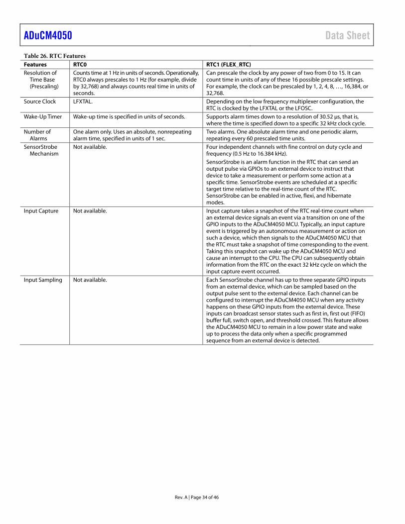
ADuCM4050 Data Sheet
Rev. A | Page 34 of 46
Table 26. RTC Features Features RTC0 RTC1 (FLEX_RTC) Resolution of
Time Base (Prescaling)
Counts time at 1 Hz in units of seconds. Operationally, RTC0 always prescales to 1 Hz (for example, divide by 32,768) and always counts real time in units of seconds.
Can prescale the clock by any power of two from 0 to 15. It can count time in units of any of these 16 possible prescale settings. For example, the clock can be prescaled by 1, 2, 4, 8, …, 16,384, or 32,768.
Source Clock LFXTAL. Depending on the low frequency multiplexer configuration, the RTC is clocked by the LFXTAL or the LFOSC.
Wake-Up Timer Wake-up time is specified in units of seconds. Supports alarm times down to a resolution of 30.52 µs, that is, where the time is specified down to a specific 32 kHz clock cycle.
Number of Alarms
One alarm only. Uses an absolute, nonrepeating alarm time, specified in units of 1 sec.
Two alarms. One absolute alarm time and one periodic alarm, repeating every 60 prescaled time units.
SensorStrobe Mechanism
Not available. Four independent channels with fine control on duty cycle and frequency (0.5 Hz to 16.384 kHz).
SensorStrobe is an alarm function in the RTC that can send an output pulse via GPIOs to an external device to instruct that device to take a measurement or perform some action at a specific time. SensorStrobe events are scheduled at a specific target time relative to the real-time count of the RTC. SensorStrobe can be enabled in active, flexi, and hibernate modes.
Input Capture Not available. Input capture takes a snapshot of the RTC real-time count when an external device signals an event via a transition on one of the GPIO inputs to the ADuCM4050 MCU. Typically, an input capture event is triggered by an autonomous measurement or action on such a device, which then signals to the ADuCM4050 MCU that the RTC must take a snapshot of time corresponding to the event. Taking this snapshot can wake up the ADuCM4050 MCU and cause an interrupt to the CPU. The CPU can subsequently obtain information from the RTC on the exact 32 kHz cycle on which the input capture event occurred.
Input Sampling Not available. Each SensorStrobe channel has up to three separate GPIO inputs from an external device, which can be sampled based on the output pulse sent to the external device. Each channel can be configured to interrupt the ADuCM4050 MCU when any activity happens on these GPIO inputs from the external device. These inputs can broadcast sensor states such as first in, first out (FIFO) buffer full, switch open, and threshold crossed. This feature allows the ADuCM4050 MCU to remain in a low power state and wake up to process the data only when a specific programmed sequence from an external device is detected.
Data Sheet ADuCM4050
Rev. A | Page 35 of 46
Beeper Driver
The ADuCM4050 MCU has an integrated audio driver for a beeper. The beeper driver module in the ADuCM4050 MCU generates a differential square wave of programmable frequency. It drives an external piezoelectric sound component with two terminals that connect to the differential square wave output.
The beeper driver consists of a module that can deliver frequencies ranging from 8 kHz to approximately 0.25 kHz; the minimum frequency is determined by the maximum value of a divide register that can be programmed to 127. This results in a beeper frequency of,
32.768 kHz/127 = 0.25802 kHz
The beeper driver allows programmable tone durations in 4 ms increments. Pulse (single-tone) and sequence (multitone) modes provide versatile playback options.
In sequence mode, the beeper can be programmed to play any number of tone pairs from 1 to 254 (2 to 508 tones) or be programmed to play forever (until stopped by the user). Interrupts are available to indicate the start or end of any beep, the end of a sequence, or when the sequence is nearing completion.
Debug Capability
The ADuCM4050 MCU supports a 2-wire serial wire debug (SWD) interface and trace feature via a single-wire viewer port. The ADuCM4050 MCU also has a full flash patch and breakpoint (FPB) unit with support for up to six hardware breakpoints.
ON-CHIP PERIPHERAL FEATURES The ADuCM4050 MCU contains a rich set of peripherals connected to the core via several concurrent high bandwidth buses, providing flexibility in system configuration as well as excellent overall system performance (see Figure 1).
The ADuCM4050 MCU contains high speed serial ports, an interrupt controller for flexible management of interrupts from the on-chip peripherals or external sources, and power management control functions to tailor the performance and power characteristics of the MCU and system to many application scenarios.
Serial Ports (SPORT)
The ADuCM4050 MCU provides two single-direction half SPORTs or one bidirectional full SPORT. The synchronous serial ports provide an inexpensive interface to a wide variety of digital and mixed-signal peripheral devices such as Analog Devices audio codecs, ADCs, and DACs. The serial ports contain two data lines, a clock, and a frame sync. The data lines can be programmed to either transmit or receive, and each data line has a dedicated DMA channel.
Serial port data can be automatically transferred to and from on-chip memory or external memory via dedicated DMA channels. The frame sync and clock can be shared. Some of the
ADCs and DACs require two control signals for their conversion processes. To interface with such devices, SPT0_ACNV and SPT0_BCNV signals are provided. To use these signals, enable the timer enable mode. In this mode, a PWM timer inside the SPORT module generates the programmable SPT0_ACNV and SPT0_BCNV signals.
Serial ports operate in two modes: the standard digital signal processor (DSP) serial mode and timer enable mode.
SPI Ports
The ADuCM4050 MCU provides three SPIs. The SPI is an industry-standard, full duplex, synchronous serial interface that allows eight bits of data to be synchronously transmitted and simultaneously received. Each SPI incorporates two DMA channels that interface with the DMA controller. One DMA channel transmits and the other receives. The SPI on the MCU eases interfacing to external serial flash devices.
The SPI features include the following:
• Serial clock phase mode and serial clock polarity mode • Loopback mode • Continuous transfer mode • Wire-OR’d output mode • Read command mode for half-duplex operation (transmit
followed by receive) • Flow control support • Multiple chip select (CS) line support • CS software override support • Support for 3-pin SPI
UART Ports
The ADuCM4050 MCU provides two full duplex UART ports that are fully compatible with PC standard UARTs. The UART port provides a simplified UART interface to other peripherals or hosts, supporting full duplex, DMA supported, asynchronous transfers of serial data. The UART port includes support for five to eight data bits, and none, even, or odd parity. A frame is terminated by one, one and a half, or two stop bits.
I2C
The ADuCM4050 MCU provides an I2C bus peripheral that has two pins for data transfer. SCL (Pin P0_04) is a serial clock pin and SDA (Pin P0_05) is a serial data pin. The pins are configured in a wire-AND’ed format that allows arbitration in a multimaster system. A master device can be configured to generate the serial clock. The frequency is programmed by the user in the serial clock divisor register. The master channel can operate in fast mode (400 kHz) or standard mode (100 kHz).
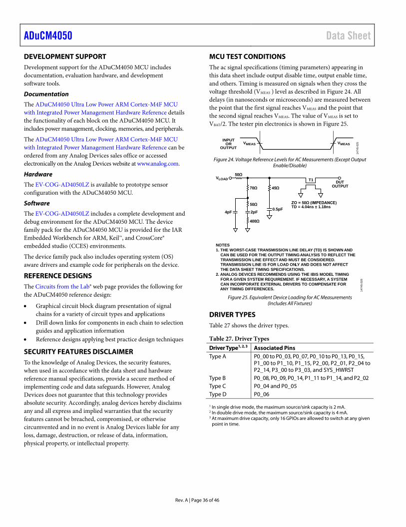
ADuCM4050 Data Sheet
Rev. A | Page 36 of 46
DEVELOPMENT SUPPORT Development support for the ADuCM4050 MCU includes documentation, evaluation hardware, and development software tools.
Documentation
The ADuCM4050 Ultra Low Power ARM Cortex-M4F MCU with Integrated Power Management Hardware Reference details the functionality of each block on the ADuCM4050 MCU. It includes power management, clocking, memories, and peripherals.
The ADuCM4050 Ultra Low Power ARM Cortex-M4F MCU with Integrated Power Management Hardware Reference can be ordered from any Analog Devices sales office or accessed electronically on the Analog Devices website at www.analog.com.
Hardware
The EV-COG-AD4050LZ is available to prototype sensor configuration with the ADuCM4050 MCU.
Software
The EV-COG-AD4050LZ includes a complete development and debug environment for the ADuCM4050 MCU. The device family pack for the ADuCM4050 MCU is provided for the IAR Embedded Workbench for ARM, Keil™, and CrossCore® embedded studio (CCES) environments.
The device family pack also includes operating system (OS) aware drivers and example code for peripherals on the device.
REFERENCE DESIGNS The Circuits from the Lab® web page provides the following for the ADuCM4050 reference design:
• Graphical circuit block diagram presentation of signal chains for a variety of circuit types and applications
• Drill down links for components in each chain to selection guides and application information
• Reference designs applying best practice design techniques
SECURITY FEATURES DISCLAIMER To the knowledge of Analog Devices, the security features, when used in accordance with the data sheet and hardware reference manual specifications, provide a secure method of implementing code and data safeguards. However, Analog Devices does not guarantee that this technology provides absolute security. Accordingly, analog devices hereby disclaims any and all express and implied warranties that the security features cannot be breached, compromised, or otherwise circumvented and in no event is Analog Devices liable for any loss, damage, destruction, or release of data, information, physical property, or intellectual property.
MCU TEST CONDITIONS The ac signal specifications (timing parameters) appearing in this data sheet include output disable time, output enable time, and others. Timing is measured on signals when they cross the voltage threshold (VMEAS ) level as described in Figure 24. All delays (in nanoseconds or microseconds) are measured between the point that the first signal reaches VMEAS and the point that the second signal reaches VMEAS. The value of VMEAS is set to VBAT/2. The tester pin electronics is shown in Figure 25.
INPUTOR
OUTPUTVMEAS VMEAS
1474
5-02
5
Figure 24. Voltage Reference Levels for AC Measurements (Except Output
Enable/Disable)
VLOAD
NOTES1. THE WORST-CASE TRANSMISSION LINE DELAY (TD) IS SHOWN AND CAN BE USED FOR THE OUTPUT TIMINGANALYSIS TO REFLECT THE TRANSMISSION LINE EFFECTAND MUST BE CONSIDERED. TRANSMISSION LINE IS FOR LOAD ONLY AND DOES NOT AFFECT THE DATA SHEET TIMING SPECIFICATIONS.2. ANALOG DEVICES RECOMMENDS USING THE IBIS MODEL TIMING FOR A GIVEN SYSTEM REQUIREMENT. IF NECESSARY, A SYSTEM CAN INCORPORATE EXTERNAL DRIVERS TO COMPENSATE FOR
ANY TIMING DIFFERENCES.
50Ω
70Ω 45Ω
ZO = 50Ω (IMPEDANCE)TD = 4.04ns ± 1.18ns50Ω
400Ω
2pF 0.5pF4pF
DUTOUTPUT
T1
1474
5-02
6
Figure 25. Equivalent Device Loading for AC Measurements
(Includes All Fixtures)
DRIVER TYPES Table 27 shows the driver types.
Table 27. Driver Types Driver Type1, 2, 3
Associated Pins Type A P0_00 to P0_03, P0_07, P0_10 to P0_13, P0_15,
P1_00 to P1_10, P1_15, P2_00, P2_01, P2_04 to P2_14, P3_00 to P3_03, and SYS_HWRST
Type B P0_08, P0_09, P0_14, P1_11 to P1_14, and P2_02 Type C P0_04 and P0_05 Type D P0_06 1 In single drive mode, the maximum source/sink capacity is 2 mA. 2 In double drive mode, the maximum source/sink capacity is 4 mA. 3 At maximum drive capacity, only 16 GPIOs are allowed to switch at any given
point in time.
Data Sheet ADuCM4050
Rev. A | Page 37 of 46
EEMBC ULPMARK™-CP SCORE Using the following software configuration and the profile configuration shown in Table 28, the EEMBC ULPMark-CP score is 189.
• Compiler name and version: IAR EWARM 8.20.1 • Compiler flags:
--no_size_constraints --cpu=Cortex-M4 -D __ADUCM4050__ --no_code_motion -Ohs -e --fpu=VFPv4_sp --endian=little
• ULPBench Profile and Version: Core Profile v1.1 • EnergyMonitor Software Version: V2.0
Table 28. EEMBC ULPMark™-CP Profile Configuration Profile Configuration Value Wake-Up Timer Module RTC1 Wake-Up Timer Clock Source External crystal Wake-Up Timer Frequency 32768 Hz Wake-Up Timer Accuracy 20 ppm Active Power Mode Name Active mode Active Mode Clock Configuration 52 MHz (CPU), 32 kHz (RTC) Active Mode Voltage Integrity 1.74 V Inactive Power Mode Name Hibernate Inactive Clock Configuration Off (CPU), 32 kHz (RTC) Inactive Mode Voltage Integrity 1.74 V
ADuCM4050 Data Sheet
Rev. A | Page 38 of 46
GPIO MULTIPLEXING The following tables capture signal multiplexing options for the GPIO pins.
Table 29. Signal Multiplexing for Port 01
Pin Multiplexed Function 0 Multiplexed Function 1 Multiplexed Function 2 Multiplexed Function 3 P0_00 GPIO00 SPI0_CLK SPT0_BCLK Not applicable P0_01 GPIO01 SPI0_MOSI SPT0_BFS Not applicable P0_02 GPIO02 SPI0_MISO SPT0_BD0 Not applicable P0_03 GPIO03 SPI0_CS0 SPT0_BCNV SPI2_RDY P0_04 GPIO04 I2C0_SCL Not applicable Not applicable P0_05 GPIO05 I2C0_SDA Not applicable Not applicable P0_06 SWD0_CLK GPIO06 Not applicable Not applicable P0_07 SWD0_DATA GPIO07 Not applicable Not applicable P0_08 GPIO08 BPR0_TONE_N Not applicable Not applicable P0_09 GPIO09 BPR0_TONE_P SPI2_CS1 Not applicable P0_10 GPIO10 UART0_TX Not applicable Not applicable P0_11 GPIO11 UART0_RX Not applicable Not applicable P0_12 GPIO12 SPT0_AD0 Not applicable UART0_SOUT_EN P0_13 GPIO13/SYS_WAKE2 Not applicable Not applicable Not applicable P0_14 GPIO14 TMR0_OUT SPI1_RDY Not applicable P0_15 GPIO15/SYS_WAKE0 Not applicable Not applicable Not applicable 1 Available in WLCSP and LFCSP.
Table 30. Signal Multiplexing for Port 11
Pin Multiplexed Function 0 Multiplexed Function 1 Multiplexed Function 2 Multiplexed Function 3 P1_00 GPIO16/SYS_WAKE1 Not applicable Not applicable Not applicable P1_01 SYS_BMODE0 GPIO17 Not applicable Not applicable P1_02 GPIO18 SPI2_CLK Not applicable Not applicable P1_03 GPIO19 SPI2_MOSI Not applicable Not applicable P1_04 GPIO20 SPI2_MISO Not applicable Not applicable P1_05 GPIO21 SPI2_CS0 Not applicable Not applicable P1_06 GPIO22 SPI1_CLK Not applicable RGB_TMR0_1 P1_07 GPIO23 SPI1_MOSI Not applicable RGB_TMR0_2 P1_08 GPIO24 SPI1_MISO Not applicable RGB_TMR0_3 P1_09 GPIO25 SPI1_CS0 Not applicable SWV P1_10 GPIO26 SPI0_CS1 SYS_CLKIN SPI1_CS3 P1_11 GPIO27 Not applicable TMR1_OUT Not applicable P1_12 GPIO28 Not applicable RTC1_SS2 Not applicable P1_13 GPIO29 TMR2_OUT Not applicable Not applicable P1_14 GPIO30 Not applicable SPI0_RDY Not applicable P1_15 GPIO31 SPT0_ACLK UART1_TX Not applicable 1 Available in WLCSP and LFCSP.
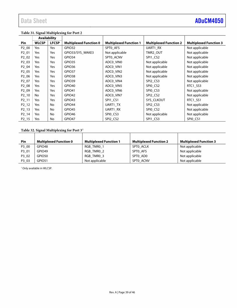
Data Sheet ADuCM4050
Rev. A | Page 39 of 46
Table 31. Signal Multiplexing for Port 2
Pin Availability
Multiplexed Function 0 Multiplexed Function 1 Multiplexed Function 2 Multiplexed Function 3 WLCSP LFCSP P2_00 Yes Yes GPIO32 SPT0_AFS UART1_RX Not applicable P2_01 Yes Yes GPIO33/SYS_WAKE3 Not applicable TMR2_OUT Not applicable P2_02 Yes Yes GPIO34 SPT0_ACNV SPI1_CS2 Not applicable P2_03 Yes Yes GPIO35 ADC0_VIN0 Not applicable Not applicable P2_04 Yes Yes GPIO36 ADC0_VIN1 Not applicable Not applicable P2_05 Yes Yes GPIO37 ADC0_VIN2 Not applicable Not applicable P2_06 Yes Yes GPIO38 ADC0_VIN3 Not applicable Not applicable P2_07 Yes Yes GPIO39 ADC0_VIN4 SPI2_CS3 Not applicable P2_08 Yes Yes GPIO40 ADC0_VIN5 SPI0_CS2 RTC1_SS3 P2_09 Yes Yes GPIO41 ADC0_VIN6 SPI0_CS3 Not applicable P2_10 No Yes GPIO42 ADC0_VIN7 SPI2_CS2 Not applicable P2_11 Yes Yes GPIO43 SPI1_CS1 SYS_CLKOUT RTC1_SS1 P2_12 Yes No GPIO44 UART1_TX SPI2_CS3 Not applicable P2_13 Yes No GPIO45 UART1_RX SPI0_CS2 Not applicable P2_14 Yes No GPIO46 SPI0_CS3 Not applicable Not applicable P2_15 Yes No GPIO47 SPI2_CS2 SPI1_CS3 SPI0_CS1
Table 32. Signal Multiplexing for Port 31
Pin Multiplexed Function 0 Multiplexed Function 1 Multiplexed Function 2 Multiplexed Function 3 P3_00 GPIO48 RGB_TMR0_1 SPT0_ACLK Not applicable P3_01 GPIO49 RGB_TMR0_2 SPT0_AFS Not applicable P3_02 GPIO50 RGB_TMR0_3 SPT0_AD0 Not applicable P3_03 GPIO51 Not applicable SPT0_ACNV Not applicable 1 Only available in WLCSP.
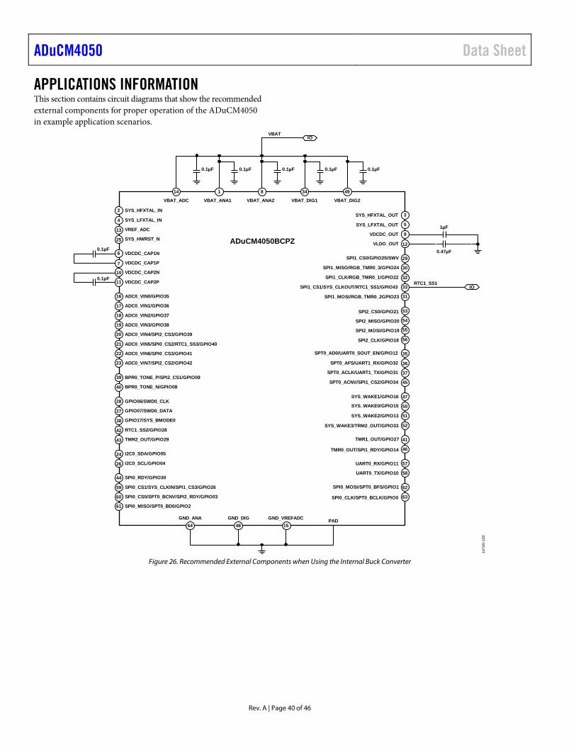
ADuCM4050 Data Sheet
Rev. A | Page 40 of 46
APPLICATIONS INFORMATION This section contains circuit diagrams that show the recommended external components for proper operation of the ADuCM4050 in example application scenarios.
0.1µF
0.1µFADuCM4050BCPZ
1µF
0.47µF
0.1µF0.1µF0.1µF0.1µF0.1µF
VBAT
RTC1_SS1
PADGND_ANA
SPI0_CLK/SPT0_BCLK/GPIO0
SPI0_MOSI/SPT0_BFS/GPIO1
SPI0_MISO/SPT0_BD0/GPIO2
SPI0_CS0/SPT0_BCNV/SPI2_RDY/GPIO03
SPI0_CS1/SYS_CLKIN/SPI1_CS3/GPIO26
UART0_TX/GPIO10
UART0_RX/GPIO11
SPI2_CLK/GPIO18
SPI2_MOSI/GPIO19
SPI2_MISO/GPIO20
SPI2_CS0/GPIO21
SYS_WAKE3/TRM2_OUT/GPIO33
SYS_WAKE2/GPIO13
SYS_WAKE0/GPIO15
VBAT_DIG2
GND_DIG
SYS_WAKE1/GPIO16
TMR0_OUT/SPI1_RDY/GPIO14
SPT0_ACNV/SPI1_CS2/GPIO34
SPI0_RDY/GPIO30
TMR2_OUT/GPIO29
RTC1_SS2/GPIO28
TMR1_OUT/GPIO27
BPR0_TONE_N/GPIO08
BPR0_TONE_P/SPI2_CS1/GPIO09
GPIO17/SYS_BMODE0
SPT0_ACLK/UART1_TX/GPIO31
SPT0_AFS/UART1_RX/GPIO32
SPT0_AD0/UART0_SOUT_EN/GPIO12
VBAT_DIG1
SPI1_CS1/SYS_CLKOUT/RTC1_SS1/GPIO43
SPI1_CLK/RGB_TMR0_1/GPIO22
SPI1_MOSI/RGB_TMR0_2GPIO23
SPI1_MISO/RGB_TMR0_3/GPIO24
SPI1_CS0/GPIO25/SWV
GPIO06/SWD0_CLK
GPIO07/SWD0_DATA
I2C0_SCL/GPIO04
SYS_HWRST_N
I2C0_SDA/GPIO05
ADC0_VIN7/SPI2_CS2/GPIO42
ADC0_VIN6/SPI0_CS3/GPIO41
ADC0_VIN5/SPI0_CS2/RTC1_SS3/GPIO40
ADC0_VIN4/SPI2_CS3/GPIO39
ADC0_VIN3/GPIO38
ADC0_VIN2/GPIO37
ADC0_VIN1/GPIO36
ADC0_VIN0/GPIO35
GND_VREFADC
VBAT_ADC
VREF_ADC
VLDO_OUT
VDCDC_CAP2P
VDCDC_CAP2N
VDCDC_OUT
VBAT_ANA2
VDCDC_CAP1P
VDCDC_CAP1N
SYS_LFXTAL_OUTSYS_LFXTAL_IN
SYS_HFXTAL_OUTSYS_HFXTAL_IN
VBAT_ANA1
IO
IO
1474
5-10
0
21
13
11
10
7
6
43
4
25
2
44
61
59
60
42
24
26
38
27
28
39
40
23
22
20
19
18
17
16
49348114
45
29
12
9
58
57
41
46
52
51
47
50
5
3
36
35
37
55
54
53
56
31
30
33
32
62
63
154864
Figure 26. Recommended External Components when Using the Internal Buck Converter
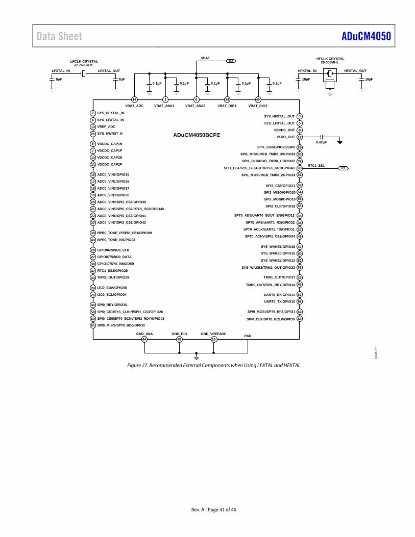
Data Sheet ADuCM4050
Rev. A | Page 41 of 46
0.47µF
RTC1_SS1IO
LFCLK CRYSTAL32.7680kHz
8pF8pF
LFXTAL_IN LFXTAL_OUT
ADuCM4050BCPZ
0.1µF0.1µF0.1µF0.1µF0.1µF
VBAT
PADGND_ANA
SPI0_CLK/SPT0_BCLK/GPIO0
SPI0_MOSI/SPT0_BFS/GPIO1
SPI0_MISO/SPT0_BD0/GPIO2
SPI0_CS0/SPT0_BCNV/SPI2_RDY/GPIO03
SPI0_CS1/SYS_CLKIN/SPI1_CS3/GPIO26
UART0_TX/GPIO10
UART0_RX/GPIO11
SPI2_CLK/GPIO18
SPI2_MOSI/GPIO19
SPI2_MISO/GPIO20
SPI2_CS0/GPIO21
SYS_WAKE3/TRM2_OUT/GPIO33
SYS_WAKE2/GPIO13
SYS_WAKE0/GPIO15
VBAT_DIG2
GND_DIG
SYS_WAKE1/GPIO16
TMR0_OUT/SPI1_RDY/GPIO14
SPT0_ACNV/SPI1_CS2/GPIO34
SPI0_RDY/GPIO30
TMR2_OUT/GPIO29
RTC1_SS2/GPIO28
TMR1_OUT/GPIO27
BPR0_TONE_N/GPIO08
BPR0_TONE_P/SPI2_CS1/GPIO09
GPIO17/SYS_BMODE0
SPT0_ACLK/UART1_TX/GPIO31
SPT0_AFS/UART1_RX/GPIO32
SPT0_AD0/UART0_SOUT_EN/GPIO12
VBAT_DIG1
SPI1_CS1/SYS_CLKOUT/RTC1_SS1/GPIO43
SPI1_CLK/RGB_TMR0_1/GPIO22
SPI1_MOSI/RGB_TMR0_2GPIO23
SPI1_MISO/RGB_TMR0_3/GPIO24
SPI1_CS0/GPIO25/SWV
GPIO06/SWD0_CLK
GPIO07/SWD0_DATA
I2C0_SCL/GPIO04
SYS_HWRST_N
I2C0_SDA/GPIO05
ADC0_VIN7/SPI2_CS2/GPIO42
ADC0_VIN6/SPI0_CS3/GPIO41
ADC0_VIN5/SPI0_CS2/RTC1_SS3/GPIO40
ADC0_VIN4/SPI2_CS3/GPIO39
ADC0_VIN3/GPIO38
ADC0_VIN2/GPIO37
ADC0_VIN1/GPIO36
ADC0_VIN0/GPIO35
GND_VREFADC
VBAT_ADC
VREF_ADC
VLDO_OUT
VDCDC_CAP2P
VDCDC_CAP2N
VDCDC_OUT
VBAT_ANA2
VDCDC_CAP1P
VDCDC_CAP1N
SYS_LFXTAL_OUTSYS_LFXTAL_IN
SYS_HFXTAL_OUTSYS_HFXTAL_IN
VBAT_ANA1
IO
1474
5-10
1
21
13
11
10
7
6
43
4
25
2
44
61
59
60
42
24
26
38
27
28
39
40
23
22
20
19
18
17
16
49348114
45
29
12
9
58
57
41
46
52
51
47
50
5
3
36
35
37
55
54
53
56
31
30
33
32
62
63
154864
HFCLK CRYSTAL26.000MHz
18pF18pF
HFXTAL_IN HFXTAL_OUT
Figure 27. Recommended External Components when Using LFXTAL and HFXTAL
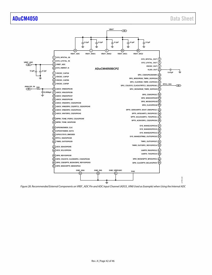
ADuCM4050 Data Sheet
Rev. A | Page 42 of 46
0.47µF
RTC1_SS1IO
0.1µF 4.7µF
0.0056µF
33Ω
VREF_ADC
ADuCM4050BCPZ
0.1µF0.1µF0.1µF0.1µF0.1µF
VBAT
PADGND_ANA
SPI0_CLK/SPT0_BCLK/GPIO0
SPI0_MOSI/SPT0_BFS/GPIO1
SPI0_MISO/SPT0_BD0/GPIO2
SPI0_CS0/SPT0_BCNV/SPI2_RDY/GPIO03
SPI0_CS1/SYS_CLKIN/SPI1_CS3/GPIO26
UART0_TX/GPIO10
UART0_RX/GPIO11
SPI2_CLK/GPIO18
SPI2_MOSI/GPIO19
SPI2_MISO/GPIO20
SPI2_CS0/GPIO21
SYS_WAKE3/TRM2_OUT/GPIO33
SYS_WAKE2/GPIO13
SYS_WAKE0/GPIO15
VBAT_DIG2
GND_DIG
SYS_WAKE1/GPIO16
TMR0_OUT/SPI1_RDY/GPIO14
SPT0_ACNV/SPI1_CS2/GPIO34
SPI0_RDY/GPIO30
TMR2_OUT/GPIO29
RTC1_SS2/GPIO28
TMR1_OUT/GPIO27
BPR0_TONE_N/GPIO08
BPR0_TONE_P/SPI2_CS1/GPIO09
GPIO17/SYS_BMODE0
SPT0_ACLK/UART1_TX/GPIO31
SPT0_AFS/UART1_RX/GPIO32
SPT0_AD0/UART0_SOUT_EN/GPIO12
VBAT_DIG1
SPI1_CS1/SYS_CLKOUT/RTC1_SS1/GPIO43
SPI1_CLK/RGB_TMR0_1/GPIO22
SPI1_MOSI/RGB_TMR0_2GPIO23
SPI1_MISO/RGB_TMR0_3/GPIO24
SPI1_CS0/GPIO25/SWV
GPIO06/SWD0_CLK
GPIO07/SWD0_DATA
I2C0_SCL/GPIO04
SYS_HWRST_N
I2C0_SDA/GPIO05
ADC0_VIN7/SPI2_CS2/GPIO42
ADC0_VIN6/SPI0_CS3/GPIO41
ADC0_VIN5/SPI0_CS2/RTC1_SS3/GPIO40
ADC0_VIN4/SPI2_CS3/GPIO39
ADC0_VIN3/GPIO38
ADC0_VIN2/GPIO37
ADC0_VIN1/GPIO36
ADC0_VIN0/GPIO35
GND_VREFADC
VBAT_ADC
VREF_ADC
VLDO_OUT
VDCDC_CAP2P
VDCDC_CAP2N
VDCDC_OUT
VBAT_ANA2
VDCDC_CAP1P
VDCDC_CAP1N
SYS_LFXTAL_OUTSYS_LFXTAL_IN
SYS_HFXTAL_OUTSYS_HFXTAL_IN
VBAT_ANA1
IO
IO
1474
5-10
2
21
13
11
10
7
6
43
4
25
2
44
61
59
60
42
24
26
38
27
28
39
40
23
22
20
19
18
17
16
49348114
45
29
12
9
58
57
41
46
52
51
47
50
5
3
36
35
37
55
54
53
56
31
30
33
32
62
63
154864
ANALOG_INIO
Figure 28. Recommended External Components on VREF_ADC Pin and ADC Input Channel (ADC0_VIN0 Used as Example) when Using the Internal ADC
Data Sheet ADuCM4050
Rev. A | Page 43 of 46
SILICON ANOMALY This anomaly list describes the known bugs, anomalies, and workarounds for the ADuCM4050. These anomalies represent the currently known differences between revisions of the ADuCM4050 product and the functionality specified in the ADuCM4050 data sheet and the hardware reference manual.
Analog Devices, Inc., is committed, through future silicon revisions, to continuously improve silicon functionality. Analog Devices tries to ensure that these future silicon revisions remain compatible with your present software/systems by implementing the recommended workarounds outlined here.
ADuCM4050 FUNCTIONALITY ISSUES Silicon Revision Identifier Silicon Status No. of Reported Anomalies 0.1 Released 3 (21000011, 21000016, 21000017)
A silicon revision number with the form x.y is branded on all devices. The silicon revision can be electronically determined by reading Bits[3:0] of the SYS_CHIPID register. SYS_CHIPID = 0x1 indicates Silicon Revision 0.1, and SYS_CHIPID = 0x0 indicates Silicon Revision 0.0.
FUNCTIONALITY ISSUES
Table 33. 21000011—I2C Master Mode Fails to Generate Clock when Clock Dividers are Too Small Issue When the I2C clock dividers are configured in master mode such that the sum of the low and high bit fields in the
I2C_DIV register is less than 16, the I2C fails to generate a clock. Workaround Program the I2C clock dividers such that I2C_DIV.LOW + I2C_DIV.HIGH ≥ 16. Revision 0.1
Table 34. 21000016—Possible Receive Data Loss with I2C Automatic Clock Stretching Issue When the I2C Rx FIFO is full and new I2C data is received, a data overflow occurs. When automatic clock stretching is
enabled, the transaction is paused by holding the SCL (Pin P0_04) line low. This function works as expected when the next read happens after the clock is stretched (that is, after the overflow is detected). However, if the read occurs after the last bit of the I2C data is received but before the clock is stretched, the received data is not written to the Rx FIFO and is lost.
Workaround When I2C automatic clock stretching is enabled, read the FIFO should only after the overflow flag is set in the status register to ensure that that Rx FIFO is never read at the same time that the overflow is asserted.
Revision 0.1
Table 35. 21000017—SPI Read Command Mode Does Not Work Properly when SPI_CNT is 1 and DMA is Enabled Issue When SPI master is enabled and uses the DMA mode with SPI_CNT = 1, the read command mode may not function
properly. Consider the following configurations: SPI_RD_CTL = 0x07; SPI_CNT = 1; the transmit and receive DMA channels are configured for 1 half-word. In this configuration, the read command sent in the first byte on the MOSI output is repeated in the second byte (in the address slot). Therefore, the slave device responds on the MISO line with whatever content is at the address equivalent to the read command value (for example, if the read command is 0xB, the response is the data read from Slave Address 0xB).
Workaround The following workarounds can be used. Utilize the overlap mode to align the transmit/receive SPI operations and discard the junk bytes, as follows: 1. Set SPI_RD_CTL.OVERLAP = 1 to enable overlap mode. 2. Set SPI_RD_CTL.TXBYTES = 1 to configure a single transmit byte (8-bit address register). 3. Set SPI_CNT.VALUE = 3 to configure the transfer count: one byte for the address register, one byte for the command,
and one dummy byte to obtain the read value. 4. On the receive side, discard the first two junk bytes received during the transfer of the address and command bytes
before processing the actual read value in the third byte. Alternatively, do not use Tx DMA operation on the SPI transmit side, by taking the following steps: 1. Enable only SPI RX DMA requests. 2. Fill the SPI Tx FIFO by using core accesses to write the SPI_TX register. 3. Perform a dummy read of the SPI_RX register to kick off the SPI transfers.
Revision 0.1
ADuCM4050 Data Sheet
Rev. A | Page 44 of 46
SECTION 1. ADuCM4050 FUNCTIONALITY ISSUES Reference No. Description Status 21000011 I2C master mode fails to generate clock when clock dividers are too small Identified 21000016 Possible receive data loss with I2C automatic clock stretching Identified 21000017 SPI read command mode does not work properly when SPI_CNT is 1 and DMA is enabled Identified
This completes the Silicon Anomaly section.
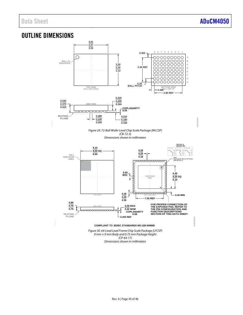
Data Sheet ADuCM4050
Rev. A | Page 45 of 46
OUTLINE DIMENSIONS
03-2
5-20
19-A
A
BCD
EFG
H
0.5300.4700.410
3.613.573.53
3.203.163.12
12345
BOTTOM VIEW(BALL SIDE UP)
TOP VIEW(BALL SIDE DOWN)
SIDE VIEW
0.2100.1800.150
0.3200.2900.260
0.2800.2400.200
2.45 REF
2.80 REF
0.35BALL PITCH
0.385
0.355 6789
COPLANARITY0.05
PKG
-005
141
BALL A1IDENTIFIER
SEATINGPLANE
Figure 29. 72-Ball Wafer Level Chip Scale Package [WLCSP]
(CB-72-3) Dimensions shown in millimeters
0.300.250.18
0.800.750.70
0.50BSC
BOTTOM VIEWTOP VIEW
6.306.20 SQ6.10
0.05 MAX0.02 NOM
0.203 REF
COPLANARITY0.08
10-2
6-20
18-A
9.109.00 SQ8.90
FOR PROPER CONNECTION OFTHE EXPOSED PAD, REFER TOTHE PIN CONFIGURATION ANDFUNCTION DESCRIPTIONSSECTION OF THIS DATA SHEET.
0.20 MIN7.50 REF
COMPLIANT TO JEDEC STANDARDS MO-220-WMMD
164
16
17
49
48
32
33
0.450.400.35
PKG
-004
559
EXPOSEDPAD
END VIEW
DETAIL A(JEDEC 95)
PIN 1IN D ICATO R AR E A OP TIO N S(SEE DETAIL A)
PIN 1INDICATOR
AREA
SEATINGPLANE
Figure 30. 64-Lead Lead Frame Chip Scale Package [LFCSP]
9 mm × 9 mm Body and 0.75 mm Package Height (CP-64-17)
Dimensions shown in millimeters
ADuCM4050 Data Sheet
Rev. A | Page 46 of 46
ORDERING GUIDE Model1 Temperature Range Package Description Package Option ADUCM4050BCBZ-RL −40°C to +85°C 72-Ball Wafer Level Chip Scale Package [WLCSP], 13” Reel CB-72-3 ADUCM4050BCBZ-R7 −40°C to +85°C 72-Ball Wafer Level Chip Scale Package [WLCSP], 7” Reel CB-72-3 ADUCM4050BCPZ −40°C to +85°C 64-Lead Lead Frame Chip Scale Package [LFCSP] CP-64-17 ADUCM4050BCPZ-RL −40°C to +85°C 64-Lead Lead Frame Chip Scale Package [LFCSP], 13” Reel CP-64-17 ADUCM4050BCPZ-R7 −40°C to +85°C 64-Lead Lead Frame Chip Scale Package [LFCSP], 7” Reel CP-64-17 EV-COG-AD4050LZ ADuCM4050 LFCSP Development Board EV-COG-AD4050WZ ADuCM4050 WLCSP Development Board 1 Z = RoHS Compliant Part.
I2C refers to a communications protocol originally developed by Philips Semiconductors (now NXP Semiconductors).
©2018–2019 Analog Devices, Inc. All rights reserved. Trademarks and registered trademarks are the property of their respective owners. D14745-0-4/19(A)