ultrahigh vacuum plasma oxidation in the...
TRANSCRIPT
Reports in Electron Physics 2000/24Espoo, September 2000
Ultrahigh Vacuum Plasma Oxidation in the Fabrication ofUltrathin Silicon Dioxide Films
Tero Majamaa
Dissertation for the degree of Doctor of Science in Technology to be presented with duepermission for public examination and debate in Auditorium S4 at Helsinki Universityof Technology (Espoo, Finland) on the 20th of October, 2000, at 12 o’clock noon.
Helsinki University of TechnologyDepartment of Electrical and Communications EngineeringElectron Physics Laboratory
Teknillinen korkeakouluSähkö- ja tietoliikennetekniikan osastoElektronifysiikan laboratorio
2
Distribution:Helsinki University of TechnologyElectron Physics LaboratoryP.O. Box 3000FIN-02015 HUTFinlandTel. +358-9-451 2322Fax. +358-9-451 5008
ISBN 951-22-5146-9ISSN 0781-4984
Otamedia OyEspoo 2000
i
Abstract
This thesis discusses the fabrication and characterization of ultrathin insulator films.
These are essential for nanoscale semiconductor device fabrication. When the insulator
layer thickness is only a few times the molecule diameter, it is crucial that both film
homogeneity and the insulator/semiconductor interface quality are as high as possible.
The small dimensions must also be taken into account in characterization, because the
established measurement techniques and analyses used in more traditional MOS
characterization are not necessarily valid any more.
In this work, the metal/silicon dioxide/silicon structure (especially oxide and
oxide/semiconductor interface quality) and various silicon dioxide fabrication methods
are discussed. The focus in the experimental work is on the studying the plasma assisted
oxidation of silicon in an ultra high vacuum chamber and on characterizing the
fabricated films. Some of the film properties are found to be excellent: interface
smoothness is of a very high quality and interface state densities are low (1011 eV-1cm-2
or lower in the mid-gap) even without any annealing. Process control also seems to be
good, as is the breakdown field. The oxide charge, however, is quite high. This may
cause considerable harm. One of the consequences is an increased leakage current. This
also significantly decreases the device life time by increasing current generated defects.
In the annealing experiments carried out, the oxide charge was seen to decrease,
indicating that the quality of the silicon dioxide films can be significantly improved by
optimization of the thermal treatments.
The molecular beam epitaxy system used in processing is designed mainly for research
purposes, offering possibility to gain much information about the oxidation process
itself. Other, and cheaper, thermal oxidation procedures have in recent years already
been developed to a very high level, which means that the process developed is not
necessarily the best choice for conventional IC manufacturing purposes. It offers,
however, useful applications for research into silicon-based nanostructures, such as
silicon/silicon dioxide heterostructures.
Keywords: Ultrathin silicon dioxide, ultrahigh vacuum, plasma oxidation

ii
iii
Preface
This thesis for the degree of Doctor of Science in Technology was mainly researched at
the Helsinki University of Technology Electron Physics Laboratory during the years
1995 - 1999. I would specially like to thank Professor Juha Sinkkonen who has
supervised my work. I also thank the other personnel of the Electron Physics
Laboratory, where I had the great privilege of working from 1990 to 1998. I owe a
special debt of gratitude to the personnel of the Microelectronics Centre at the Helsinki
University of Technology and VTT Electronics for the use of their clean room facilities
and equipment as well as for many helpful conversations and invaluable advise.
I am also grateful to the Academy of Finland for the generous financial support they
granted to the research project during my years at the Electron Physics Laboratory as
well as for the encouragement of my co-workers and superiors since I started at the
Academy.
Tero Majamaa

iv
v
List of Symbols
a,A,a0,B,G0,k,l0,r,τ
constants
A area
Ai Airy function
B susceptance
C capacitance
C0 oxygen concentration on sample surface
C1 concentration of oxidizing molecules
Cgr growth site concentration
CHF high frequency capacitance
Cit interface trap state capacitance
CLF low frequency capacitance
COX oxygen concentration on silicon dioxide surface
CS oxygen concentration at silicon/silicon dioxide interface
Cox,s saturated oxide capacitance
Cmos MOS capacitance
CSI oxygen concentration on silicon surface
D diffusion coefficient
Dit surface state density
d0 initial thickness of the silicon dioxide layer
dcr critical thickness of a silicon dioxide layer
dox oxide thickness
dsc depletion region length
E energy, electric field
EA activation energy
Ec conduction band energy
Ef Fermi energy
Eg energy bandgap
En0 electron ground state energy in potential well
Eox electric field in the silicon dioxide
Ep0 hole ground state energy in potential well
Es electric field at the silicon/silicon dioxide interface
vi
Ev valence band energy
F flux, modulation factor
f frequency
(g) gas
G conductance
Gmos leakage conductance through MOS structure
h Planck constant
i imaginary unit
J current density
JDT current density in direct tunneling
JFN current density in Fowler-Nordheim tunneling
k wave number
kB Boltzmann coefficient
m mass
m* effective mass
ni intrinsic carrier concentration
ns electron density at the silicon/silicon dioxide interface
NA acceptor density
N A− density of ionized acceptors
ND donor density
N D+ density of ionized donors
Nox oxide charge density
Ns silicon/silicon dioxide interface charge density
p hole density
ps hole density at the silicon/silicon dioxide interface
P pressure
P0 reference pressure
q unit charge
Q charge
r relative sticking coefficient
R resistance
Rit interface trap state resistance
Rs series resistance
(s) solid
vii
t time
T temperature
V potential, voltage
Vbi built in voltage
Vfb flat band voltage
∆Vfb flat band voltage shift
Vg gate voltage
Vox voltage across the oxide
Vs potential at the silicon/silicon dioxide interface
Vtrap potential of a interface trap level
X reactance
Y admittance
Ym measured admittance
Z impedance
Zm measured impedance
δ Dirac delta function
ε dielectric constant
εSi dielectric constant of silicon
εOx dielectric constant of silicon dioxide
ΦM barrier height at metal/oxide interface
ΦSi barrier height at silicon/oxide interface
ρ charge density
ω angular frequency
Abbreviations
ALCVD Atomic Layer CVD
ALD Atomic Layer Deposition
ALE Atomic Layer Epitaxy
CMOS Complementary MOS
CV Capacitance - Voltage
CVD Chemical Vapor Deposition
viii
FET Field Effect Transistor
FN Fowler-Nordheim (tunneling)
IC Integrated Circuit
Imag imaginary part
LF Low Frequency
LPCVD Low Pressure CVD
MBD Molecular Beam Deposition
MBE Molecular Beam Epitaxy
MOS Metal Oxide Semiconductor
MOSFET Metal Oxide Semiconductor Field Effect Transistor
NMOS n-channel MOS
NTP Normal Temperature and Pressure
PECVD Plasma Enhanced CVD
PEE Plasma Enhanced Evaporation
PMOS p-channel MOS
Real real part
RF Radio Frequency
RHEED Reflection High Energy Electron Diffraction
RPECVD Remote Plasma Enhanced CVD
RTD Resonance Tunneling Diode
RTA Rapid Thermal Annealing
RTO Rapid Thermal Oxidation
SILC Stress Induced Leakage Current
SOI Silicon on Insulator
TEM Transmission Electron Microscopy
UHV Ultra High Vacuum
UPO Ultrahigh vacuum Plasma Oxidation
XPS X-ray Photo emission Spectroscopy
ix
Contents
1 Introduction ................................................................................................................ 1
2 MOS Structure ........................................................................................................... 5
2.1 Silicon/Silicon Dioxide Interface ........................................................................ 6
2.2 Tunneling, Leakage, Breakdown and Defect Generation ................................. 10
3 Fabrication of Thin Silicon Dioxide Films .............................................................. 16
3.1 Cleaning of the Substrate Surface ..................................................................... 16
3.2 Thermal Oxidation............................................................................................. 19
3.2.1 Deal-Grove Model ...................................................................................... 24
3.3 Other Fabrication Methods................................................................................ 26
3.4 Annealing .......................................................................................................... 29
4 Electrical Characterization of Ultrathin Insulators .................................................. 34
4.1 Oxide Charge..................................................................................................... 36
4.2 Impedance of Thin Oxide MOS Structure......................................................... 37
4.3 Oxide Thickness ................................................................................................ 42
4.4 Surface State Density ........................................................................................ 45
5 Ultrahigh Vacuum Plasma Oxidation (UPO)........................................................... 49
5.1 Equipment.......................................................................................................... 50
5.2 Electrical Characterization ................................................................................ 51
5.3 Oxidation Rate................................................................................................... 51
5.3.1 Experiment.................................................................................................. 52
5.4 Room Temperature Oxidation........................................................................... 58
5.4.1 Experiment.................................................................................................. 59
5.5 Effect of Oxidation Temperature on the Silicon Dioxide Quality .................... 63
5.5.1 Experiment.................................................................................................. 63
5.6 The Effect of Post Oxidation Annealing ........................................................... 68
5.6.1 Experiment.................................................................................................. 69
5.7 Evaporation Technique...................................................................................... 72
5.7.1 Experiment.................................................................................................. 73
6 Conclusions .............................................................................................................. 78

x
1
1 Introduction
During 1994 research interests at the Helsinki University of Technology Electron
Physics Laboratory started to shift increasingly from III-V compounds towards silicon
based devices. With the growing interest to use our molecular beam epitaxy (MBE)
system to fabricate silicon devices, it became obvious that, in addition to epitaxial
semiconductor layers, it was also necessary to have some thin insulator films. This
paved the way to our research on plasma oxidation in ultra high vacuum (UHV) 1,2,3,4.
Molecular beam epitaxy systems have been used in submicron MOSFET fabrication 5,6,
but these processes usually do not include oxidation in the MBE. There has, however,
been some work on cyclotron resonance plasma oxidation in UHV 7 or some other
oxidation/evaporation methods 8, for instance. In our research the aim was to maximize
the process purity and the quality of the materials produced by performing the oxidation
in an ultra high vacuum MBE system. The use of an MBE system allows for highly
accurate growth and there are almost no impurities at all. Our processing equipment also
provides the possibility for in situ native oxide removal and device processing, which
further improves process purity. This process not only allows us to fabricate high
quality films, but also makes it possible to get a more reliable picture on the oxidation
process on an atomic level.
The main impetus for our research was provided by the growing interest worldwide in
silicon/silicon dioxide based nanodevices. The aim has been to fabricate ever smaller
and faster devices and circuits. The decrease in the chip area, and by the same token in
the processing linewidths, means that the vertical dimensions of the devices also have to
decrease. This requires a fabrication method that produces very homogeneous and high
quality Si/SiO2 interfaces and SiO2 layers with accurately defined thickness. A 50-nm
channel length bulk MOSFET would have a 2-nm thick gate oxide for high performance
applications. That would give a maximum electric field of 5 MV/cm in the oxide, about
half of the breakdown field of good quality bulk oxide 9. Normal operation of a
MOSFET with an ultra-thin direct-tunneling gate oxide was first achieved in November
1995. In an n-MOSFET, with 1.5 nm gate oxide and 100 nm gate length,
transconductance above 10 S/cm and current drive above 1 mA/µm was measured at
2
room temperature 16. By decreasing the channel length of MOSFET to 80 nm and the
oxide thickness to 3.5 nm, cut-off frequencies of about 100 GHz have been reached 9.
Other silicon based devices in which ultrathin oxides are needed include, for instance,
memory structures based on silicon nanocrystals 10.
The tightening of process tolerances in order to satisfy more stringent defect density and
reliability requirements poses many difficult challenges. For purposes of fabricating
faster sub-micrometer MOSFETs and quantum devices, the thickness of the silicon
dioxide layer may be no more than a couple of nanometers. This greatly enhances the
impact of surface roughness scattering on drain current and carrier mobility 11. The
surface and the interface have to be flat on an atomic scale. Roughness may also
enhance tunneling currents. Furthermore, roughness increases the amount of traps and
charge at the interface, creates extra energy states, and leads to local variations in the
electric field and in the channel charge. It is widely accepted that low frequency 1/f
noise in MOS transistors is due to mobility or charge fluctuations arising from dynamic
trapping and detrapping of channel carriers by interface traps.
As the dimensions are reduced to the level where quantum effects begin to appear, it
also becomes possible to use silicon to fabricate versatile new devices, which could
earlier only be made from compound semiconductors. This would mean increased
process compatibility and reduced circuit prices. Research so far has produced such
innovations as luminescent silicon/silicon dioxide heterostructures, for instance 12.
Because the energy gap in silicon dioxide is above 8 eV and in silicon 1.1 eV and the
affinity of silicon is over 3 eV higher than in silicon dioxide (Figure 1.1), the barriers
can be much higher and quantum wells much deeper than in III-V heterostructures. This
means there can exist more quantum states at the same time, and quantum phenomena
can be utilized in room temperature. The state energies can be adjusted by changing the
quantum well dimensions.
Research on silicon-based nanodevices has also involved some trials to fabricate
resonant tunneling diodes (RTDs), but the resonant effect achieved has not been very
strong 13. The quality of the interface between these two materials is not as good as
when using crystalline materials with low lattice mismatch, such as GaAs and AlGaAs.
This means that there always exist interface states and consequently there are several
3
possible states from which and to which the carriers can tunnel. For this reason it is hard
to see clear quantum effects. The strongest silicon based photon emission, also, has been
reached by using porous or multicrystalline silicon: not silicon/silicon dioxide
heterostructures. The origin of this luminescence is not clear, but it might be due to
some three dimensional quantum structures, formed by nanocrystals.
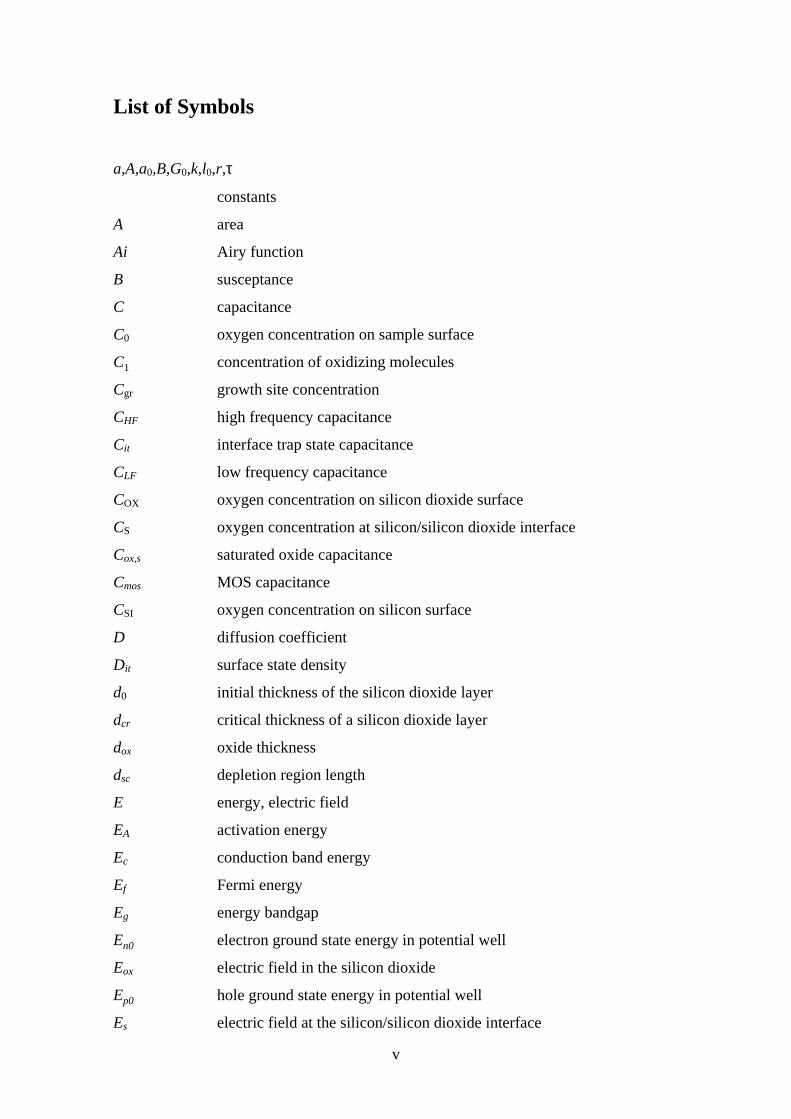
Figure 1.1 Schematic illustration of energy band structure of a a) RTD b) silicon/silicondioxide heterostructure. Ep0 and En0 represent the ground state energies in the potentialwells.
Another major problem has to do with the fact that silicon dioxide is an amorphous
material, and the average distances between silicon atoms in silicon lattice and in silicon
dioxide are different. Because of the ’lattice mismatch’ it is difficult to grow single

4
crystalline silicon on top of the oxide without holes through the oxide or in some other
way so that the epitaxial layer can come into direct contact with the substrate. After that
high temperature treatment is also usually needed to transform multicrystalline material
into single crystal. Some experiments have, however, succeeded in growing single
crystal silicon on SiOx, where the oxygen content is about 20 at.% or less (x < 0.25) 14.
This, of course, means that the oxide properties are changed.
There has been intensive research on the outermost limit of the downscaling of silicon
dioxide films. A decrease in device size, and the oxide thickness leads to an increase in
the tunneling current. Tunneling can have a significant effect on the transistor operation.
The stress induced leakage current (SILC) is considered to be the major limiting factor
for the downscaling of tunnel oxides. If the devices operate at elevated temperatures,
SILC increases. Present estimates are that the film thickness can not go much below
2.2 nm (1 V supply voltage) 15. After that the reliability decreases too much. Various
fabrication procedures and the set-ups for experimentation result, however, slightly
different properties. Device structures can also be modified to improve performance
without extended downscaling. One of the ways of tackling the problems occurring in
the ultrathin region has, in fact, been to change the MOSFET structure rather than just
scale down the dimensions 16. The drain and source wells can be made deeper, which
decreases sheet resistance. Smaller gate decreases leakage current and increases drain
current. Nonuniform channel doping in both vertical and lateral directions can be used
to minimize the short channel effects, while low temperature CMOS and double gate
MOSFETs can potentially lead to the outermost limit of silicon scaling 9. SOI and SiGe
devices offer performance and power advantages over bulk CMOS without channel
length scaling. The demands of the rapidly developing semiconductor industry will,
however, still require even smaller dimensions and thinner silicon dioxide films.
5
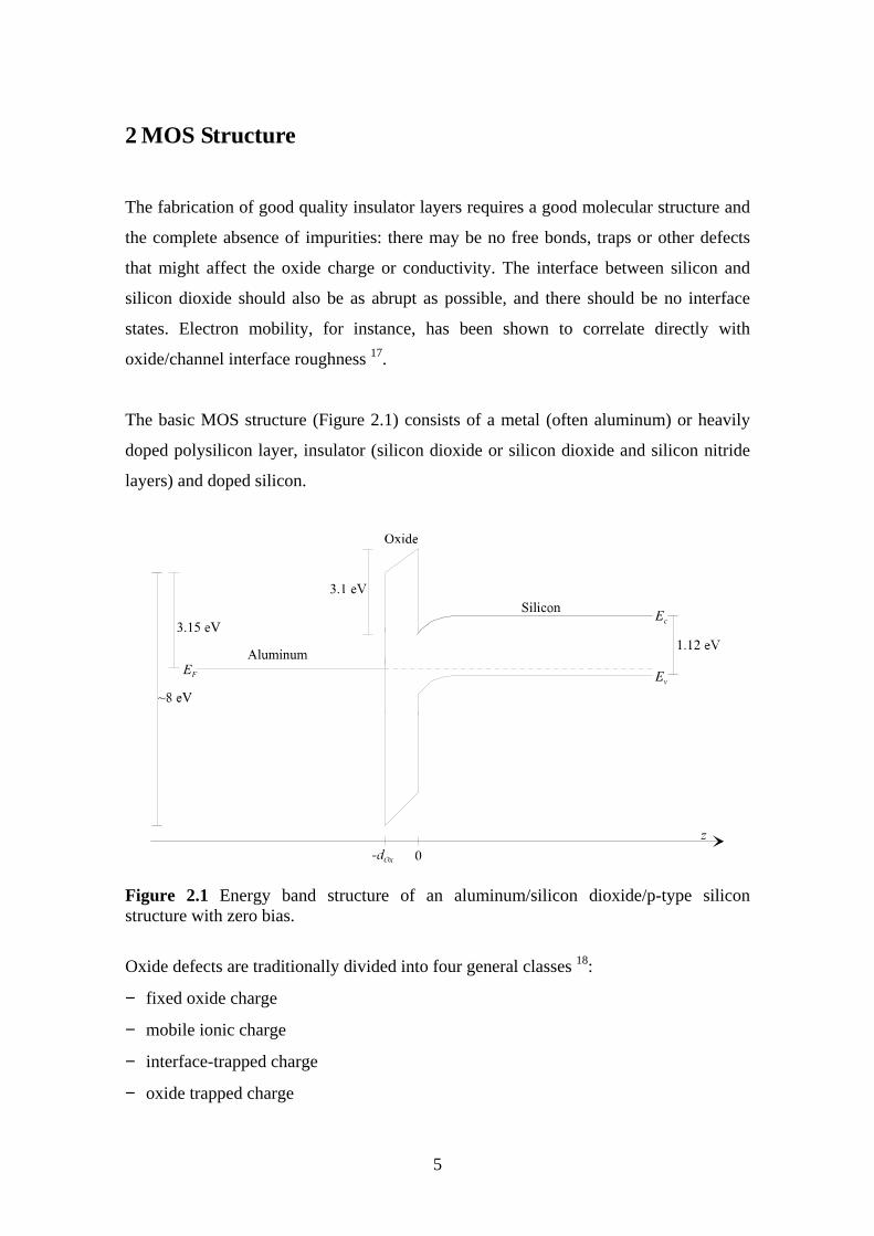
2 MOS Structure
The fabrication of good quality insulator layers requires a good molecular structure and
the complete absence of impurities: there may be no free bonds, traps or other defects
that might affect the oxide charge or conductivity. The interface between silicon and
silicon dioxide should also be as abrupt as possible, and there should be no interface
states. Electron mobility, for instance, has been shown to correlate directly with
oxide/channel interface roughness 17.
The basic MOS structure (Figure 2.1) consists of a metal (often aluminum) or heavily
doped polysilicon layer, insulator (silicon dioxide or silicon dioxide and silicon nitride
layers) and doped silicon.
Figure 2.1 Energy band structure of an aluminum/silicon dioxide/p-type siliconstructure with zero bias.
Oxide defects are traditionally divided into four general classes 18:
− fixed oxide charge
− mobile ionic charge
− interface-trapped charge
− oxide trapped charge
6
Interface traps communicate directly with the underlying silicon, whereas oxide traps
and fixed charge do not. There are also so-called ‘border traps’ 19, a term applied to
traps lying within about 3 nm of the silicon/silicon dioxide interface and in
communication with the silicon. These are near-interfacial oxide traps that can either
rapidly or slowly exchange charge with the silicon. They play an important role in
determining low frequency (1/f) noise levels in MOS transistors. Border traps can act
like either interface traps or bulk oxide traps, depending on the bias and the time scale.
They include so-called ‘slow states’ 20, ‘anomalous positive charge’ 21 and rechargeable
E’ centers 22. It must be noted that all defects in ultrathin oxides may act as border traps,
since the film thickness is on the 3-nm scale, or even lower.
Impurities also have an impact on energy band discontinuity at the silicon/silicon
dioxide interface 23. They induce changes in the band structure and have been found to
bring about a decrease in conduction band off-set and an increase in valence band off-
set. The evidence suggests these changes are almost identical in thermal oxide 23. The
magnitude of the energy gap is thus not changed, but the bands are bended. The
variations in the energy band structure between the bulk oxide and the interface region
depend of course on the impurity concentration and the oxide quality. In some
conventional dry oxidation experiments (below 800 oC) a typical value for the off-set
shift has found to be about 0.2 eV, on both silicon (100) as on silicon (111)
surfaces 24,25. This value can be reduced, however, by using ultra clean processes 23.
2.1 Silicon/Silicon Dioxide Interface
Almost all silicon wafers that are used in microelectronics are single crystalline. Silicon
dioxide, on the other hand, is amorphous. The average distances between atoms also
differ from one another. Once the silicon surface is oxidized, the interface between
these two materials can no longer be perfect. The volume per silicon atom in silicon
dioxide is about twice that in silicon crystal, which means that silicon atoms are
inevitably emitted from the interface to release stress during oxidation 26. The atomic
scale structure of the interface between crystalline silicon and its amorphous oxide
7
remains controversial 27. However, a very high degree of perfection has been achieved
in practice, which is evidenced by the very low density of defects observed at the
interface.
Depending on the oxidation procedure interface roughness between silicon and silicon
dioxide layer has been reported to be up to 1 - 1.6 nm 28,29. Roughness is also affected
by surface orientation and film thickness. On (100) surfaces there is less roughness than
on (111) surfaces, but it increases with increasing thickness (film thickness 1 nm,
roughness about 0.06 nm; film thickness 2 nm, roughness 0.14 nm 30). On (111)
surfaces, however, the range of roughness depends hardly at all on thickness (about
0.3 nm 30), but the horizontal size of the protrusions increases with film thickness.
Several assumptions have been made about the possible interfacial structure of the
silicon/silicon dioxide interface. Non-reacted silicon - silicon bonds have been observed
at the interface by means of Auger spectroscopy. On this basis it can be assumed that
there is at least one monolayer of silicon dioxide into which some amorphous silicon is
mixed 31. Auger analysis has also shown that there is an interface layer in which there is
less oxygen and usually some silicon clusters 32. The same effect has been reported on
the basis of ellipsometric measurements 33, where the change in the refractive index
shows lower oxygen contents. There have also been made some measurements of the
structural nature of silicon/silicon dioxide interface (oxide thickness 5 - 27 nm) by using
infrared absorption associated with oxygen vibrational modes 29. These measurements
indicated that the interface difference is mainly due to stoichiometric changes, not to
stress or densification.
The interface region width depends not only on the substrate and oxide layer fabrication
procedure, but also on the measurement techniques used. This is because there are in
fact two kinds of distinct regions near the interface: compositional and structural
transition layers 34. The compositional transition occurs abruptly within one silicon
atomic layer, which due to cross linking consists of intermediate oxidation states 35,
such as Si1+, Si2+ and Si3+. The structural transition, by contrast, takes a much greater
extent from the bulk silicon to bulk silicon dioxide. On the silicon side it consists of one
or two silicon monolayers in which the atomic arrangement differs from the bulk 36.
Computer simulations of oxygen transport into silicon and the formation of bonds
8
indicate that within the first monolayer there are extra silicon atoms due to stress, before
oxygen diffuses into the silicon network 27,37. The same simulations provide a partial
explanation for the low interface defect densities 27: during oxidation the oxygen atoms
can momentarily be bonded to three silicon atoms, which allows the interface to evolve
without leaving dangling bonds.
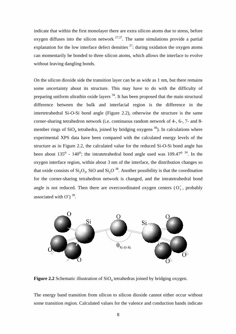
On the silicon dioxide side the transition layer can be as wide as 1 nm, but there remains
some uncertainty about its structure. This may have to do with the difficulty of
preparing uniform ultrathin oxide layers 34. It has been proposed that the main structural
difference between the bulk and interfacial region is the difference in the
intertetrahedral Si-O-Si bond angle (Figure 2.2), otherwise the structure is the same
corner-sharing tetrahedron network (i.e. continuous random network of 4-, 6-, 7- and 8-
member rings of SiO4 tetrahedra, joined by bridging oxygens 38). In calculations where
experimental XPS data have been compared with the calculated energy levels of the
structure as in Figure 2.2, the calculated value for the reduced Si-O-Si bond angle has
been about 135o - 140o; the intratetrahedral bond angle used was 109.47o 34. In the
oxygen interface region, within about 3 nm of the interface, the distribution changes so
that oxide consists of Si2O3, SiO and Si2O 38. Another possibility is that the coordination
for the corner-sharing tetrahedron network is changed, and the intratetrahedral bond
angle is not reduced. Then there are overcoordinated oxygen centers ( O3+ , probably
associated with O-) 39.
Figure 2.2 Schematic illustration of SiO4 tetrahedras joined by bridging oxygen.
The energy band transition from silicon to silicon dioxide cannot either occur without
some transition region. Calculated values for the valence and conduction bands indicate
9
that it takes about 0.4 - 0.5 nm before the energy gap corresponds to the bulk values,
even for an ideal interface between silicon and crystalline silicon dioxide 42. This is
consistent with simulations 27 indicating that the stoichiometry of the first 0.5 nm of
oxide is close to SiO.
Results have been published according to which there might be some crystalline silicon
dioxide near the interface, maintaining an epitaxial relation with the substrate 40.
However, it is estimated that the concentration of these crystallites is low (possibly a
few percent) and they are probably unstable 41. Thus, the possibility to form a totally
crystalline transition layer is highly dependent on the oxidation process. One very
prominent suggestion is that in an optimal case, the transition layer between crystalline
silicon and amorphous silicon dioxide could be an ordered, about 0.5 nm-thick
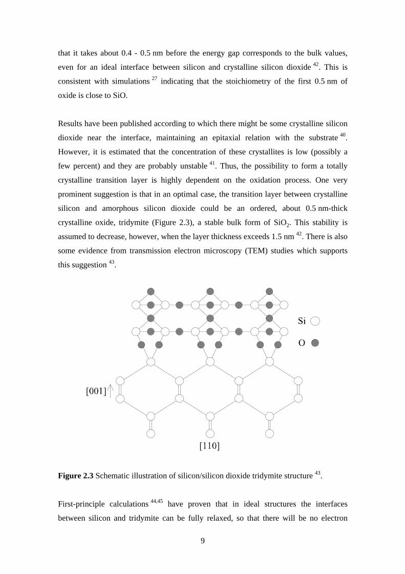
crystalline oxide, tridymite (Figure 2.3), a stable bulk form of SiO2. This stability is
assumed to decrease, however, when the layer thickness exceeds 1.5 nm 42. There is also
some evidence from transmission electron microscopy (TEM) studies which supports
this suggestion 43.
Figure 2.3 Schematic illustration of silicon/silicon dioxide tridymite structure 43.
First-principle calculations 44,45 have proven that in ideal structures the interfaces
between silicon and tridymite can be fully relaxed, so that there will be no electron
10
states in the silicon gap. In these calculations it has been assumed that a tridymite is
attached to the silicon (100) surface and the strain is localized to a transition region at
the interface and does not persist in the bulk oxide 45. The width of the transition region,
0.5 nm, accommodates the required change in silicon density. The amount of suboxide
of 1.5 monolayers is compatible with the best experimental results. The structure
corresponds to a local energy minima, but there might also be other minimas that are
even lower 45. Therefore in order to fabricate such crystals, the process has to be very
accurately controlled.
2.2 Tunneling, Leakage, Breakdown and Defect Generation
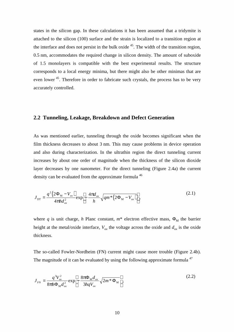
As was mentioned earlier, tunneling through the oxide becomes significant when the
film thickness decreases to about 3 nm. This may cause problems in device operation
and also during characterization. In the ultrathin region the direct tunneling current
increases by about one order of magnitude when the thickness of the silicon dioxide
layer decreases by one nanometer. For the direct tunneling (Figure 2.4a) the current
density can be evaluated from the approximate formula 46
( ) ( )Jq V
hd
d
hqm Vox
ox
oxoxDT
MM=
−− −
2
2
2
4
42
ΦΦ
ππ
exp * ,(2.1)
where q is unit charge, h Planc constant, m* electron effective mass, ΦM the barrier
height at the metal/oxide interface, Vox the voltage across the oxide and dox is the oxide
thickness.
The so-called Fowler-Nordheim (FN) current might cause more trouble (Figure 2.4b).
The magnitude of it can be evaluated by using the following approximate formula 47
Jq V
h d
d
hqVmFN
ox
ox
ox
ox
= −
3 2
28
8
32
ππΦ
ΦΦ
M
MMexp * ,
(2.2)
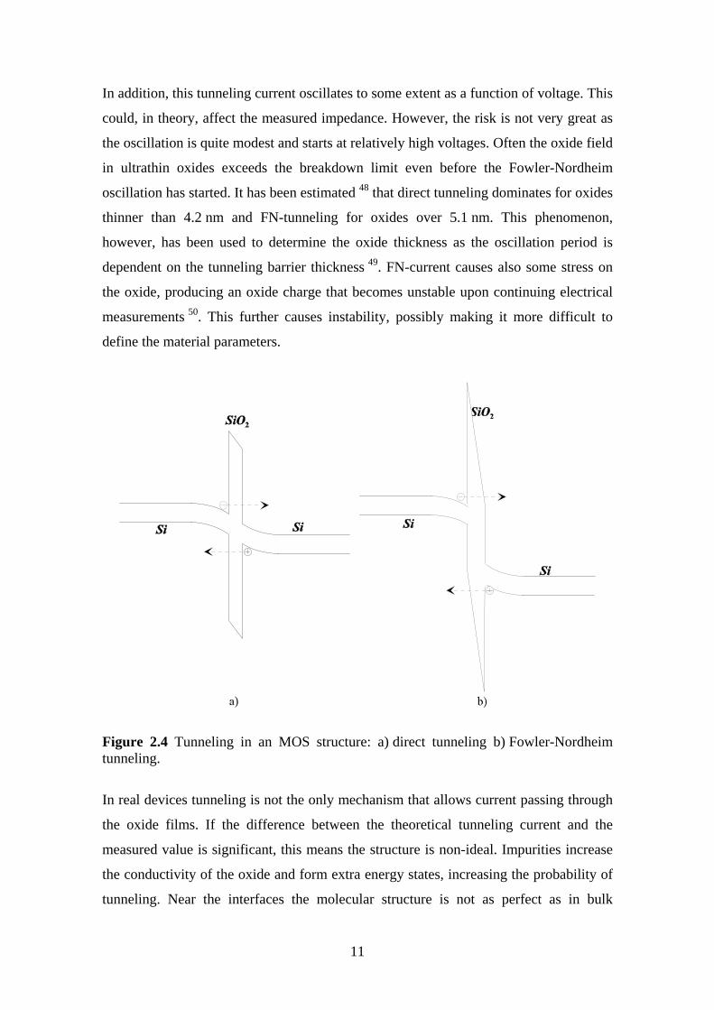
11
In addition, this tunneling current oscillates to some extent as a function of voltage. This
could, in theory, affect the measured impedance. However, the risk is not very great as
the oscillation is quite modest and starts at relatively high voltages. Often the oxide field
in ultrathin oxides exceeds the breakdown limit even before the Fowler-Nordheim
oscillation has started. It has been estimated 48 that direct tunneling dominates for oxides
thinner than 4.2 nm and FN-tunneling for oxides over 5.1 nm. This phenomenon,
however, has been used to determine the oxide thickness as the oscillation period is
dependent on the tunneling barrier thickness 49. FN-current causes also some stress on
the oxide, producing an oxide charge that becomes unstable upon continuing electrical
measurements 50. This further causes instability, possibly making it more difficult to
define the material parameters.
Figure 2.4 Tunneling in an MOS structure: a) direct tunneling b) Fowler-Nordheimtunneling.
In real devices tunneling is not the only mechanism that allows current passing through
the oxide films. If the difference between the theoretical tunneling current and the
measured value is significant, this means the structure is non-ideal. Impurities increase
the conductivity of the oxide and form extra energy states, increasing the probability of
tunneling. Near the interfaces the molecular structure is not as perfect as in bulk
12
material, which also affects the energy band structure. That may significantly reduce the
potential barrier height. Various kinds of lattice defects may create conductive channels
through the insulator. Because the dimensions are small, any kinds of impurities may
diffuse, or spike, through the layers, especially during high temperature processing. The
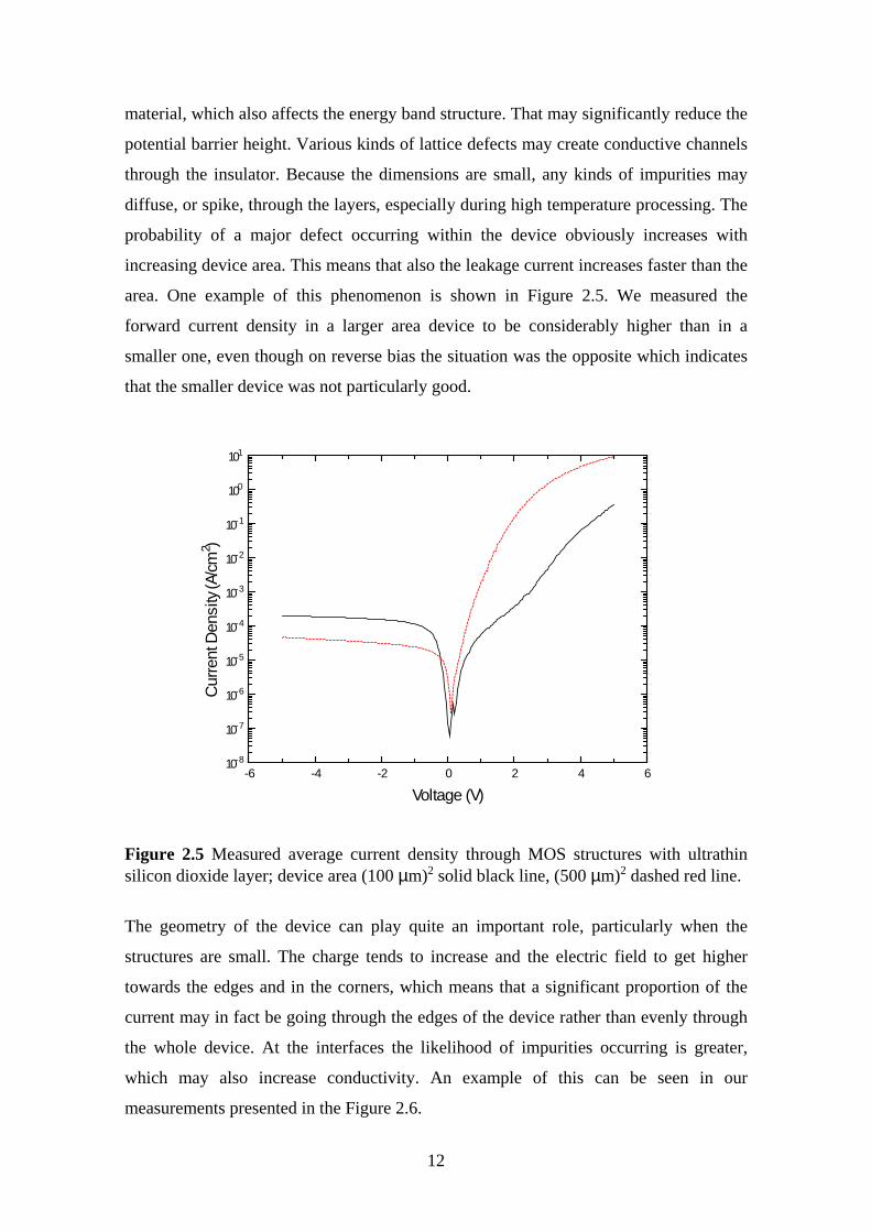
probability of a major defect occurring within the device obviously increases with
increasing device area. This means that also the leakage current increases faster than the
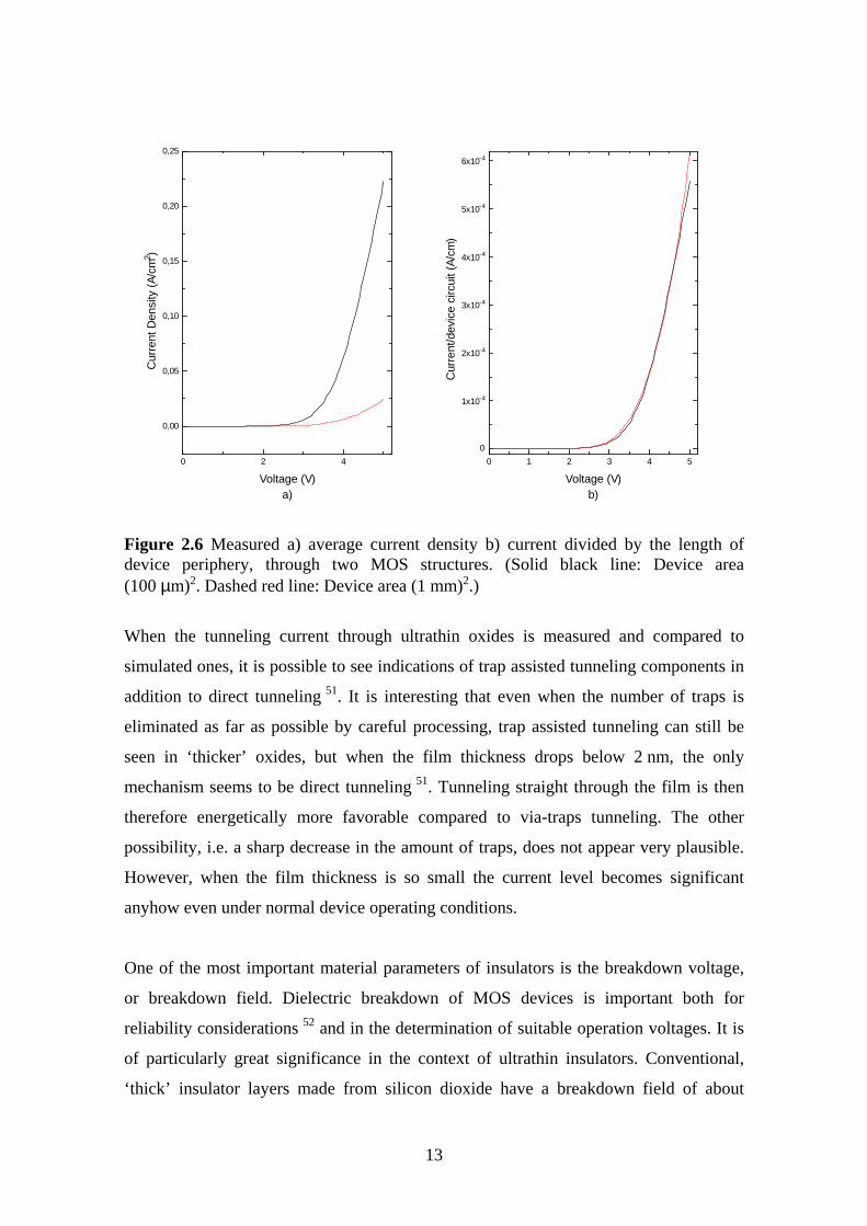
area. One example of this phenomenon is shown in Figure 2.5. We measured the
forward current density in a larger area device to be considerably higher than in a
smaller one, even though on reverse bias the situation was the opposite which indicates
that the smaller device was not particularly good.
-6 -4 -2 0 2 4 610-8
10-7
10-6
10-5
10-4
10-3
10-2
10-1
100
101
Cur
rent
Den
sity
(A/c
m2 )
Voltage (V)
Figure 2.5 Measured average current density through MOS structures with ultrathinsilicon dioxide layer; device area (100 µm)2 solid black line, (500 µm)2 dashed red line.
The geometry of the device can play quite an important role, particularly when the
structures are small. The charge tends to increase and the electric field to get higher
towards the edges and in the corners, which means that a significant proportion of the
current may in fact be going through the edges of the device rather than evenly through
the whole device. At the interfaces the likelihood of impurities occurring is greater,
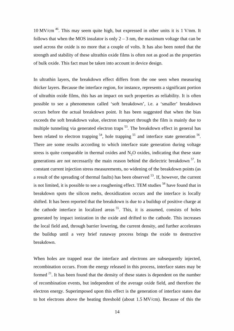
which may also increase conductivity. An example of this can be seen in our
measurements presented in the Figure 2.6.
13
0 2 4
0,00
0,05
0,10
0,15
0,20
0,25C
urre
nt D
ensi
ty (
A/c
m2 )
Voltage (V)a)
0 1 2 3 4 5
0
1x10⁻⁴
2x10⁻⁴
3x10⁻⁴
4x10⁻⁴
5x10⁻⁴
6x10⁻⁴
Cur
rent
/dev
ice
circ
uit (
A/c
m)
Voltage (V)b)
Figure 2.6 Measured a) average current density b) current divided by the length ofdevice periphery, through two MOS structures. (Solid black line: Device area(100 µm)2. Dashed red line: Device area (1 mm)2.)
When the tunneling current through ultrathin oxides is measured and compared to
simulated ones, it is possible to see indications of trap assisted tunneling components in
addition to direct tunneling 51. It is interesting that even when the number of traps is
eliminated as far as possible by careful processing, trap assisted tunneling can still be
seen in ‘thicker’ oxides, but when the film thickness drops below 2 nm, the only
mechanism seems to be direct tunneling 51. Tunneling straight through the film is then
therefore energetically more favorable compared to via-traps tunneling. The other
possibility, i.e. a sharp decrease in the amount of traps, does not appear very plausible.
However, when the film thickness is so small the current level becomes significant
anyhow even under normal device operating conditions.
One of the most important material parameters of insulators is the breakdown voltage,
or breakdown field. Dielectric breakdown of MOS devices is important both for
reliability considerations 52 and in the determination of suitable operation voltages. It is
of particularly great significance in the context of ultrathin insulators. Conventional,
‘thick’ insulator layers made from silicon dioxide have a breakdown field of about
14
10 MV/cm 46. This may seem quite high, but expressed in other units it is 1 V/nm. It
follows that when the MOS insulator is only 2 – 3 nm, the maximum voltage that can be
used across the oxide is no more that a couple of volts. It has also been noted that the
strength and stability of these ultrathin oxide films is often not as good as the properties
of bulk oxide. This fact must be taken into account in device design.
In ultrathin layers, the breakdown effect differs from the one seen when measuring
thicker layers. Because the interface region, for instance, represents a significant portion
of ultrathin oxide films, this has an impact on such properties as reliability. It is often
possible to see a phenomenon called ‘soft breakdown’, i.e. a ‘smaller’ breakdown
occurs before the actual breakdown point. It has been suggested that when the bias
exceeds the soft breakdown value, electron transport through the film is mainly due to
multiple tunneling via generated electron traps 53. The breakdown effect in general has
been related to electron trapping 54, hole trapping 55 and interface state generation 56.
There are some results according to which interface state generation during voltage
stress is quite comparable in thermal oxides and N2O oxides, indicating that these state
generations are not necessarily the main reason behind the dielectric breakdown 57. In
constant current injection stress measurements, no widening of the breakdown points (as
a result of the spreading of thermal faults) has been observed 53. If, however, the current
is not limited, it is possible to see a roughening effect. TEM studies 58 have found that in
breakdown spots the silicon melts, deoxidization occurs and the interface is locally
shifted. It has been reported that the breakdown is due to a buildup of positive charge at
the cathode interface in localized areas 55. This, it is assumed, consists of holes
generated by impact ionization in the oxide and drifted to the cathode. This increases
the local field and, through barrier lowering, the current density, and further accelerates
the buildup until a very brief runaway process brings the oxide to destructive
breakdown.
When holes are trapped near the interface and electrons are subsequently injected,
recombination occurs. From the energy released in this process, interface states may be
formed 21. It has been found that the density of these states is dependent on the number
of recombination events, but independent of the average oxide field, and therefore the
electron energy. Superimposed upon this effect is the generation of interface states due
to hot electrons above the heating threshold (about 1.5 MV/cm). Because of this the
15
defect generation rate also increases sharply 21.
Thin oxides stressed at high voltages have increased low level pre-tunneling leakage
currents 59. The leakage seems to be localized, not uniform. It is assumed to be due to
tunneling through stress-generated positive centers 60, or local lowering of tunneling
barrier due to the generation of local defects 61. Higher pre-tunneling currents and lower
breakdown distributions have been related to oxygen deficiencies at the silicon/silicon
dioxide interface 62. The intrinsic oxide decomposition reaction Si + SiO2 → 2SiO at the
interface is supposed to be nucleated at existing defect sites prior to the growth of
physical voids. These defects can become electrically active during annealing at
temperatures lower (e.g. below 900 oC in UHV) than needed for void formation. Unless
sufficient O2 is available, this can lead to low field dielectric breakdown 62.
It has been found that an increase in pre-tunneling currents correlates with the number
of traps generated within the oxide by high voltage stress 59. Low field leakage currents
introduced in the thin oxide during high field stress are related to defects produced by
hot electron transport 63. The generation of neutral electron traps is assumed to be the
dominant cause of this phenomenon. Atomic hydrogen exposure causes similar
leakages, supporting the conclusion that currents are related to hydrogen induced
defects 63. Oxide trap distribution is relatively uniform, and trap density increases as the
cube root of the fluence of electrons passing through the film 59. The trapped electrons
in stressed oxides seem to be located primarily at border traps: it has been estimated that
the centroid of the trapped positive charge lies as close as 1.2 nm to the silicon/silicon
dioxide interface 64. Capacitance-voltage (CV) characteristics analysis of thin oxides
stressed at Fowler-Nordheim region have also shown slow traps quite near the interface
(charge centroid located up to 2.5 nm from the interface) 65. The interface trap density
increases as the square root of the stress fluence 59. The high electric fields near the
interface and/or reduced barriers to local tunneling, or charge injection caused by hole
trapping, may trigger border trap formation as a natural response to increasing local
electric fields 64. It is, however, also possible to see an annealing effect of the defects
with increasing temperature 66.
16
3 Fabrication of Thin Silicon Dioxide Films
3.1 Cleaning of the Substrate Surface
On the surface of silicon wafers, along with possible contamination, there is a native
oxide layer whose thickness is typically a couple of nanometers. This native oxide has
to be completely removed in order that a good quality thin oxide film can be produced
on silicon surface. It is also required that the sample surface is flat on an atomic scale,
because the thin oxide morphology seems to reflect the original surface of the wafer 67.
It is also important that the substrate, its cleaning procedures and other processing
stages are carefully selected. It has been shown 68 that oxide defects in thin films can be
associated with substrate defect: the defect density on Czohralski -silicon can be nearly
one order of magnitude larger than that for Float-Zone silicon. However, these defects
can be removed by a sacrifice oxidation procedure, in which the oxide thickness is at
least 0.4 µm. Etching of the substrate surface does not alone seem to suffice 68.
Usually the wafers are first cleaned by using some chemical cleaning procedure, such as
so-called RCA cleaning:
− 5 minute ultrasonic in acetone
− 5 minute isopropyl alcohol
− 10 minutes in H2O:NH4OH:H2O2 (5:1:1) at 80 oC
− 10 minutes in H2O:HCl:H2O2 (5:1:1) at 80 oC
Better results have been achieved by using 77:
− 10 minutes rinsing in deionized water
− twice 5 minutes in methyl alcohol agitation
− 15 minutes boil in trichloroethylene
− twice 5 minutes in methyl alcohol agitation
− rinsing in water
− 10 minutes in 69% HNO3 in 130 oC
− 10 s dips in 2.5% HF followed by rinsing in water until the surface becomes
17
hydrophobic
− 10 minutes in 25% NH4OH: 30% H2O2:H2O (1:1:3) in 90 oC
− 10 s dip in HF
− rinsing in water
− 10 minutes in 37% HCl:H2O2:H2O (3:1:1) in 90 oC
− 10 minutes rinsing in water
Chemical cleaning procedures are used to remove all unwanted impurities from the
surface. The resulting surface is usually of a good enough quality for the fabrication of
conventional semiconductor devices. After chemical cleaning, it is possible to passivate
the surface by HF treatment, for instance, which will prevent reactions with oxygen in
the air or some other oxidizing species in the environment. This passivation, however, is
seldom perfect and even at best will not last for long. Recently it has also been
demonstrated 69 that the presence of a chemical oxide barely affects growth kinetics or
uniformity.
The best way to remove the oxide is to do it in situ. This means it is done immediately
before the beginning of oxidation and in the same processing equipment, reducing the
risk of sample contamination. Excellent results have been reported with this method
(e.g. thickness control of the layers fabricated and interface smoothness) 17. The most
common methods of in situ native oxide removal are plasma etching or the heating of
the sample in an oxygen free environment (in UHV or in inert gas, depending on the
process equipment). Since plasma etching is expected to roughen the surface, the
heating procedure is often preferred. During heating following reaction will occur 70
2SiO2(s) → 2SiO(g) + O2(g),
and reaction products will desorb form the surface. In situ plasma cleaning with
hydrogen has also been found to be suitable for silicon MBE processes (e.g. ref. 71).
Studies of oxygen desorption from silicon surfaces in UHV conditions have found that
the desorption starts inhomogenously, mainly at defect sites 72. Voids are therefore
formed at these sites. Low co-ordination number silicon monomers transform to be free
18
mobile monomers, which diffuse (within the voids) and are incorporated into a reactive
oxide complex at the silicon/oxide boundary. The reactive SiOx complex and the
addition of silicon atoms can then form SiO(g), which desorbs from the surface 72. This
reaction consumes silicon, which means there will form a pit into the silicon surface at
the defect site.
An atomically flat silicon surface can be produced by flashing (heating rapidly) the
substrate to 1200 oC 73. Even though the silicon melting point is around 1400 oC, its
surface may start (incompletely) to melt at around 1150 – 1200 oC in ultrahigh vacuum
conditions; there may occur some sublimation of silicon even at lower temperatures
(though still above 1000 oC) 74. The use of high temperatures seems to smoothen the
surface. Interface roughness has been measured both from RCA cleaned and from
samples that were RCA cleaned and flashed at 1200 oC in UHV before thermal
oxidation at 900 oC 75. It was found that if only chemical methods are used to clean the
substrate, roughness increases as the layer thickness decreases from about 10 nm,
reaching its maximum at a layer thickness of 4 nm. In UHV cleaned samples, however,
roughness decreases with decreasing layer thickness. It is, however, not always practical
or even possible to use such high temperatures. It has been shown that at these
temperatures oxygen vacancies and charge traps are formed and there might exist some
gettering which roughens the silicon/silicon dioxide interface 76.
In our case the processing equipment is a UHV chamber. Thus the native oxide can be
removed simply by heating the sample. We can verify the desorption of the silicon
dioxide layer by monitoring the surface by RHEED (Reflection High Energy Electron
Diffraction): when the surface turns into a clean, monocrystalline silicon surface, the
RHEED pattern becomes clear. Even a thin native oxide layer totally prevents the
pattern to be formed. We have used two different native oxide removal procedures. The
first consists simply in heating the sample to 875 oC at 10-10 - 10-9 mbar 1. The native
oxide is then removed in less than 15 minutes. The second procedure we have used has
been shown to produce an excellent surface, entirely clean and flat by removing the
native oxide by keeping the sample at 850 oC and etching the oxide off by a low silicon
flux 77. When some silicon is introduced into the surface in gas form, the reaction Si +
SiO2(s) → 2SiO(g) happens on the surface, not in the silicon/silicon dioxide interface.
For this reason bulk silicon consumption should be lower than in conventional methods.
19
This probably explains why this method produces quite flat surfaces, even though the
temperature is not that high. In fact, it has been suggested that even 780 oC may be
enough, given the background pressure of 7.10-11 mbar 73 and the chamber pressure of
1.5.10-9 mbar during silicon deposition. In our experiments 2-4 we have used this lower
temperature and seen that the native oxide is removed quite quickly, within one minute.
3.2 Thermal Oxidation
Thermal oxidation is the most common, and also the simplest way to produce silicon
dioxide layers. In microelectronics device processing the best silicon/silicon dioxide
interfaces are fabricated by thermal oxidation of (100) silicon 78. When the sample is
heated in an oxygen-containing atmosphere, its surface becomes oxidized. The oxygen
is normally introduced in gas form (‘dry oxidation’), but sometimes water vapor (‘wet
oxidation’) is used. It is also possible to use oxygen plasma, which increases the
oxidation rate, but in this case the process is more sensitive and it might increase
interface roughness and defect density (e.g. 79). This is because the plasma may also
etch the surface.
The main process parameters affecting the oxidation rate, and also the oxide and
interface quality, are temperature and oxygen concentration. An increase in either one of
these also increases the oxidation rate and the maximum layer thickness that can be
achieved. Oxidation temperature is the most important process parameter affecting
oxide quality; the hotter the better. Oxidation at high temperatures minimizes interface
roughness and produces the best quality material. In practice this is also seen in
decreasing interface trap density 80.
The most usual reactions
Si + O2 → SiO2 and Si + 2H2O → SiO2 + 2H2
are also reversible. If the desorption rate from the surface is high enough, this may
increase surface roughness. The presence of hydrogen during oxidation, or annealing
20
oxides in a hydrogen-containing atmosphere, is usually considered to have beneficial
effects on oxide quality. The addition of hydrogen has the beneficial property of
rendering charge traps inactive 46. One must, however, be careful in adjusting the
process, because there is evidence that the introduction of extra hydrogen into the oxide
may also aid in the creation of interface traps 81.
During the early stages of thin oxide growth the interface between silicon and its
thermal oxide undergoes atomic scale roughening 82. This reaches its peak and then
begins to diminish as growth proceeds. This is also an indication of a nonuniform
oxidation process: the growth of about 1 nm protrusions can be explained by a reduction
in the interface reaction rate brought about by local stress effects 82. At temperatures
above about 950 - 975 oC, oxide films grow stress-free, which is attributed to the
‘viscous flow’ of the oxide 83. The temperature limit above which this is possible is
called the ‘viscous flow point’. Relaxation of the silicon dioxide layer by this viscous
flow and the transition to diffusion controlled growth act to eliminate roughness. This is
reported to peak at a layer thickness of about 4 nm 82. Another defect-density-maximum
has also been found in Czohralski silicon wafers 84, with the oxide defect density
increasing with increasing film thickness between 5 and 40 nm, and decreasing above
80 nm. The dependence of defect density on thickness is probably much affected by the
substrate, impurity concentrations and oxidation procedure: for instance the ‘60 nm
defect maximum’ has not been found when using Float-Zone substrates 84. It has also
been noted that even thick oxides with seemingly low oxide defect densities do in fact
contain many small defects. These, too, may have serious adverse effects on oxide
reliability. This quality decrease is probably caused by oxygen molecules diffusing
through the oxide 82. With increasing thickness, the diffusion slows down. At the
beginning, on the other hand, there is less oxide structure to be damaged in the first
place.
First-principle calculations of stresses affecting the process have shown that a uniform
oxide layer can be obtained with any thickness by thermal oxidation once a uniform
surface oxide layer has been formed 26. Therefore the preparation of the initial surface
oxide is crucial for obtaining a uniform surface oxide layer with atomically controlled
thickness.
21
The ‘rapid thermal oxidation’ (RTO) process is in widespread use in the fabrication of
thin oxide films. Typically this is done by oxidizing silicon with O2 or by using N2O.
The results have been excellent, and the processes are now so refined that thickness can
be controlled to the accuracy of a few Angstroms. On the thickness scale of 2 - 5 nm,
thickness can be controlled within 10% 85. The temperatures used are typically between
700 - 1200 oC, and the oxidation time is around one minute. After the oxidation of
ultrathin layers 85 the surface state densities can be as high as 1012 eV-1cm-2 but they can
be reduced by annealing to the level of 1010 eV-1cm-2. In the RTO method, too,
increasing temperature decreases leakage current and fixed charge density, but it has
also been found to decrease breakdown voltage 86. This may be due to pinholes or to
defects created by the high temperature processing into the oxide.
It is predicted that the interface quality declines when the oxidation temperature is
below the viscous flow point of the oxide 82. Using temperatures above this point helps
to avoid mechanical failure effects in IC-processing. High temperatures, which are
usually needed to fabricate good quality layers, also increase the oxidation rate and
therefore make it harder to adjust the film thickness. However, good results have been
achieved by using ultra clean processes and low partial pressures of oxygen in some
inert gases like argon 87, or low pressure oxidation 88. These not only help to achieve
more precise thickness control, but also a thickness uniformity may be improved 17.
This does not, however, mean that oxidation times would not be much shorter than in
conventional thermal oxidation. The oxide properties also tend to differ, sometimes
quite considerably, when the oxidation parameters are changed 89.
There has also been some research to study the use of temperatures lower than in RTO
(in practice usually above 650 oC 90) in the fabrication of ultrathin silicon dioxide
layers. However, at temperatures below 1000 oC there may occur stress-induced
dislocations and edge cracking. The problems have been tackled by reducing oxidation
times to no more than a few seconds 31. On the other hand, oxidation at lower
temperatures can produce layers comparable to high temperature oxides. As well as
giving improved thickness control, low temperature processing also prevents
degradation of device performance due to the redistribution of impurities and the
formation of stress-induced defects in silicon 91. There still are, however, problems with
low temperature oxidation: the oxidation rate is slow, and the oxidation also saturates
22
too early to form a layer thick enough for microelectronics purposes. To increase the
film growth rate, and especially to make it possible to fabricate slightly thicker layers,
additional techniques have been developed. It has been demonstrated 92 that by using
high pressure oxidation (10 bar), the temperature can be lowered to 650 oC and the
oxide still shows excellent characteristics. The use of activated oxygen and low pressure
also makes it possible to use low temperatures (300 - 500 oC) and still produce high
quality properties 93.
A typical way of increasing the growth rate is to use plasma instead of oxygen gas (or
N2O gas or water vapor). This allows the oxidation temperature to be dropped by a
couple of hundred degrees, say to 600 oC 94,95, or if no more than about two nanometers
are needed, even as low as 400 oC 96. This is due to the smaller size and increased
reactivity of oxygen atoms as compared to the ‘traditional’ oxidizing molecules,
molecular oxygen or water. To carry out oxidation at room temperature, one possibility
is to use a low energy ion beam 97 or a multipolar electron cyclotron resonance source
for plasma generation 98. One method that has been used to fabricate high quality silicon
dioxide films at room temperature (up to 11 nm) is oxidation by O2 cluster ion beams 91.
In this case less damage will be caused by the beam, since the acceleration energy is
divided between the single atoms of the cluster. It follows that the atom interactions
occur near the surface. Some annealing is needed after this process, but it has been
found that 30 minutes at 400 oC should be enough 91.
Nitrided Oxides
N2O has recently become an increasingly popular oxidizing gas. The main benefits
achieved with N2O in oxidation, or post oxidation nitridation of conventionally oxidized
layers, are the improved breakdown properties 52,99. There is less degradation under hot
electron stress and resistance to hot carrier induced interface state generation also
improves with increasing N concentration 100,101. It has been reported that increased
nitrogen concentration in the silicon/silicon dioxide interface increases interface state
densities, but decreases the tunneling current. This current reduction has been estimated
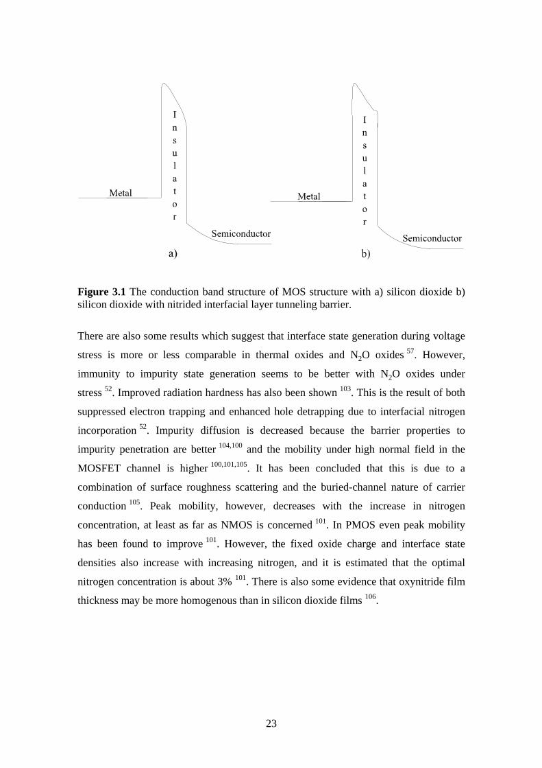
to be about one decade at any film thickness from 2.5 to 5 nm 102. This, it is assumed, is
due to the increase in the area of the tunneling barrier (Figure 3.1). The growth rate is
also significantly lower, helping with process adjustment 31,100.
23
Figure 3.1 The conduction band structure of MOS structure with a) silicon dioxide b)silicon dioxide with nitrided interfacial layer tunneling barrier.
There are also some results which suggest that interface state generation during voltage
stress is more or less comparable in thermal oxides and N2O oxides 57. However,
immunity to impurity state generation seems to be better with N2O oxides under
stress 52. Improved radiation hardness has also been shown 103. This is the result of both
suppressed electron trapping and enhanced hole detrapping due to interfacial nitrogen
incorporation 52. Impurity diffusion is decreased because the barrier properties to
impurity penetration are better 104,100 and the mobility under high normal field in the
MOSFET channel is higher 100,101,105. It has been concluded that this is due to a
combination of surface roughness scattering and the buried-channel nature of carrier
conduction 105. Peak mobility, however, decreases with the increase in nitrogen
concentration, at least as far as NMOS is concerned 101. In PMOS even peak mobility
has been found to improve 101. However, the fixed oxide charge and interface state
densities also increase with increasing nitrogen, and it is estimated that the optimal
nitrogen concentration is about 3% 101. There is also some evidence that oxynitride film
thickness may be more homogenous than in silicon dioxide films 106.
24
3.2.1 Deal-Grove Model
In the conventional, so-called Deal-Grove model used for oxidation rate calculations in
thermal oxidation 46,107, an oxygen flux creates an oxygen concentration C0 on the
surface. Oxygen diffuses through the existing silicon dioxide layer (thickness z) into the
silicon. When the oxygen concentration in the silicon/silicon dioxide interface is CS, the
flux is defined as
z
CCD
dz
dCDF S0
1−
≈= ,(3.1)
where D is the diffusion coefficient. The oxygen molecules coming to the silicon/silicon
dioxide interface react with silicon at a rate that is proportional to the concentration.
This requires the flux
F2 = kCS . (3.2)
When
F = F1 = F2 , (3.3)
the oxidation rate is
kDz
D
C
C
C
F
dt
dz
+==
1
0
1
,(3.4)
where C1 is the concentration of oxidizing molecules in the silicon dioxide. The time
needed to grow a layer of thickness z can be calculated from equation (3.4). The result is
( )[ ] 002
02 ,
1dzdzAdz
Bt >−+−= ,
(3.5)
where d0 is the oxide thickness at the beginning. The parameters B/A ≡ 2kC0/C1 and
25
B ≡ 2DC0/C1, which are usually referred to as linear and parabolic rate constants,
possess the temperature dependence exp(-EA/kBT) 46.
The Deal-Grove model assumes that there always exists an initial oxide layer through
which the oxidizing molecules have to penetrate and that this diffusion process is the
main factor limiting the growth (diffusion limited growth). The parabolic growth
behavior presented in equation (3.5) has been verified down to an oxide thickness of
5 nm 87. As the thickness of the insulator layer needed for MOS devices decreases
below 20 nm, some experiments 108 (thermal oxidation in atmospheric pressure and
temperatures around 1000 oC) have, however, indicated that the Deal-Grove model
tends to underestimate the initial growth rate. Therefore an extension has been
developed to this model 108. Here the parameter k from equation (3.2) assumes the form
k rC→ gr , (3.6)
where Cgr is the concentration of so-called growth sites in the silicon/silicon dioxide
interface. These are suggested to be sites formed by silicon suboxides, silicon clusters or
interestial atoms that can react with the oxidizing species.
The growth site concentration changes due to a generation mechanism (which is
assumed to have an Arrhenius-type temperature dependence) and to recombination, in
which the dominating factors are the concentration of these sites and the amount of the
silicon atoms. The atom concentration is constant, therefore
dC
dtG e CE k TA Bgr
gr= −−0
1
τ,
(3.7)
and since we are talking about ultrathin layers, the growth rate is about the same as the
linear rate constant
( )τ−−
=+≈=≈ tTkE
smallx
ealeCC
Cr
A
B
dt
dzBA
00gr1
0 .(3.8)
26
On this basis the initial growth rate is exponential rather than constant. Deductions
made from simulations of quantum molecular dynamics suggest that there might indeed
be a very fast oxidation step that precedes the diffusion limited growth. It has been
estimated that the oxide layer has to be at least about 0.7 nm thick before the oxidation
becomes diffusion limited 109.
3.3 Other Fabrication Methods
One of the most common ways of fabricating thin silicon dioxide layers in
microelectronics is by the means of chemical vapor deposition (CVD). In this method
the oxide, and especially the electrical quality of the silicon/silicon dioxide interface, is
not as good as in thermal oxidation, but the use of post oxidation annealing has
produced some good results. In fact results have been published according to which the
MOSFET transconductance can be even higher than in devices in which the gate oxide
is fabricated by thermal oxidation. One possible reason for this is the smoother
silicon/silicon dioxide interface, which is defined only by the original high quality
silicon surface 110. It is also possible that the explanation lies in some resultant tensile
stress in the oxide 111. The higher oxide charge may also have some effect, rejecting
carriers from the interface and thus decreasing the interfacial roughness scattering.
The plasma enhanced CVD (PECVD) method is widely used in microelectronics, not
least on account of its low processing temperatures, usually below 350 oC. Using this
method, silicon dioxide layers have been fabricated 112 (at 250 oC) in which after
annealing the surface state densities are in the range of 1 - 4.1010 cm-2eV-1. These values
are comparable to thermally grown layers. Hydrogenated silicon oxide films have also
been fabricated by PECVD at temperatures as low as 15 - 150 oC 113. However, this
tends to produce a low oxygen concentration (SiOx:H, x < 2) and a porous film
structure. This precludes applications in devices, but it is still possible to take advantage
of the fact that the layer will be easily oxidized 113.
In plasma assisted processes there is the risk that the exited oxidizing species may
damage the substrate surface upon impact. For this reason there has been quite a lot of
27
interest in the low pressure CVD (LPCVD; e.g. 0.13 mbar 114 or ≤ 0.01 mbar 115)
process. This process gives a slower growth rate and thus allows for easier control of the
thickness of ultrathin layers. In this process the silane and oxygen are mixed prior to
entering the reactor, and deposition is achieved by a pyrolytic process at the substrate
surface 114. In remote plasma enhanced CVD (RPECVD) the process temperature can be
lower. The activation energy in the process is also much lower, about one order of
magnitude, than in thermal oxidation 93. It must also be noted that if higher temperatures
are used in RPECVD, some thermal oxidation will occur and affect film growth 93.
As-grown chemical oxides are uniform, have a low density, and contain a variety of
defects such as Si-H bonds, dangling bonds, voids and OH groups, both in the oxide and
at the interface. Therefore in order to reach gate oxide quality, it is necessary to have
high temperature (800 - 1000 oC) process stages 116. For example absorbed hydrocarbon
contaminants dissociate and become chemically incorporated into thin oxides as
additional silicon oxide, carbide, hydrid and hydroxyl species. In UHV conditions these
persist up to the SiO desorption temperature (up to 850 - 1000 oC) so that once formed,
these defects will be present in the final device structure 116.
Deposited (LPCVD at 420 oC, as well as RPECVD at 300 oC) thin oxides show
enhanced Fowler-Nordheim tunneling currents compared with thermal oxides, even
after some high temperature (750 oC 40 minutes N2-O2 117) annealing. They also exhibit
very large electron trapping, with the traps reside close to the silicon/silicon dioxide
interface 117. It has also been reported that after annealing layer quality (oxide fixed
charge and surface state density) can be comparable to thermal oxides, although the
measured electron barrier height is still significantly lower 114.
To maximize the benefits achieved by the low temperature CVD process and to
combine those with the high quality interface properties achieved with thermal
oxidation, a two-step process has also been used 118. Here a low trap-density
silicon/silicon dioxide interface has been fabricated by plasma assisted oxidation. After
this the ‘bulk oxide’ is made by RPECVD deposition of silicon dioxide with device
quality properties. The first stage, which produces an oxide film about 0.5 nm thick,
also removes carbon residuals from the surface and prevents nitrogen incorporation at
the interface.
28
As mentioned earlier in chapter 3.2, nitrogen incorporation into the oxide improves
some insulator properties. CVD can also be used to grow these nitrided oxide films. The
difference between these silicon dioxide and nitrided films are quite similar to thermal
oxides: above 3% the positive oxide charge increases linearly with the nitrogen
concentration, and above 4% there is also a sharp decline in mobility 119.
The silicon surface can also be oxidized chemically, for instance simply by keeping it in
a hydrogen peroxide solution. This gives a very slow oxidation process, however, and it
is only possible to produce very thin layers. This oxidation procedure has been tested by
oxidizing monohydride terminated atomically flat silicon (111) wafers in an ultrapure
30% H2O2 solution at room temperature 120. The first bilayer was oxidized within 30
minutes and then the process saturates; after two months only 60% of the next bilayer
has been oxidized. This is obviously not a practical procedure for producing layers for
most device applications: the tunneling probability is too high (chapter 2.2). Also, the
average composition of the first bilayer is about SiO1.2, and hence the layer quality does
certainly not correspond to the properties of SiO2.
Another way to fabricate thin silicon dioxide layers on silicon is to use the method of
anodic oxidation. By using NH4OH:H2O 121 or 0.1M HCl 122, for instance, as
electrolyte, it is possible to grow layers 1 - 10 nm thick. The resulting oxide thickness is
strongly dependent on the visible illumination intensity 123, which can be used to adjust
the process.
The atomic layer epitaxy (ALE, also Atomic Layer Deposition (ALD) or Atomic Layer
CVD) method has also been used to fabricate thin silicon dioxide layers. One of the
binary reaction sequences used is (asterisks indicate the surface species) 124
SiOH* + SiCl4 → SiOSiCl3* + HCl
SiCl* + H2O → SiOH* + HCl
As each of the half-reactions is self-limiting, growth is controlled layer by layer. The
resulting surfaces are very flat 125, as flat as the original silicon substrate surfaces. The
measured deposition per one processing cycle (at 330 oC and 1 - 13 mbar) is only
29
0.11 nm. This is quite interesting as one silicon dioxide monolayer should be more than
two times that. This might mean that the layer is strongly ordered. The ‘growth rate’, i.e.
the thickness of one deposited layer, decreases with increasing temperature (at least
between 330 and 530 oC 125), which correlates with the thermal stability of the SiOH*
surface functional groups 126. The other reaction used in ALE 127 is based on the
deposition of CH3OSi(NCO)3 and H2O2. This process can be performed at room
temperature with a deposition rate of 0.2 nm/cycle. After 100 cycles surface roughness
is only ±1.0 nm, but the measurements indicate that the layers formed are silicon rich
(SiO1.73).
Thermal oxidation produces higher quality material than any other method, but all of
these other methods are nonetheless usable, if not for MOSFETs or tunneling devices
then at least for other purposes. Poor quality oxide may even result in higher intensity
light emission for instance. Although the method of sputtering, for example, is quite a
’rough’ way of making such fine structures as nanometer scale silicon/silicon dioxide
devices, it has been used to fabricate some luminescent structures. The results seem
very encouraging, but the usability of these layers in electronic devices remains to be
established. In photoluminescent devices the non-homogeneity of the silicon dioxide
and the grain boundaries may even serve to improve the luminescence. The main
benefits of sputtering are its low costs and low processing temperatures. On the other
hand, the interface state densities tend to be high and the breakdown fields too low 128.
One of the methods employed in an attempt to improve the layer quality has been to
carry out the sputtering in an oxygen-containing atmosphere and to use some post
oxidation rapid thermal annealing (RTA). RTA has been found to drop the interface
state densities to the level of 1.8.1012 eV-1cm-2 and by post metallization anneal
(350 oC) to 3.5.1011 eV-1cm-2 129. A lowering of the sputtering pressure also seems to
produce better layers.
3.4 Annealing
Device processing always involves in practice some post oxidation thermal treatments.
Annealing after oxidation decreases the amount of oxide charge and the silicon/silicon
30
dioxide interface trap density. There are two basic annealing procedures: low
temperature annealing, which typically continues for tens of minutes, and rapid thermal
annealing at high temperatures.
Although the general preference is for high temperatures, it has been shown that
temperatures as low as 300 - 400 oC are sufficient to decrease the surface state
densities. Values between 1.1010 and 5.1010 cm-2eV-1 have been measured after
annealing from samples fabricated by the PECVD method 112,115.
When studying high temperature annealings, it has been observed that a few minutes of
annealing (at 900 oC 28) reduces trap density exponentially as a function of time.
Interface roughness, especially on the (100) surface, has also been reported to decrease
dramatically during post oxidation annealing. In RTA experiments 129 an increase in
annealing time (50 - 500 s) has been found to be more effective in decreasing interface
trap densities than an increase in annealing temperature (700 oC - 1000 oC). Oxygen
defects and traps are removed 86, and the strain between the silicon and oxygen bonds is
probably also relieved. There is also some evidence that an increase in temperature
decreases leakage current. The underlying mechanism may be an increase in barrier
height. If, however, the temperature rises above 1000 oC, the barrier height might on the
contrary decrease 86.
Dealing as we are with ultrathin layers and processing in high vacuum conditions, high
temperature processing gives rise to certain problems. Diffusion or spiking may quite
easily cause impurities to penetrate into or even through these films. It has also been
noted 130 that voids are formed in about 1 nm thick layers when annealed at 750 oC.
This is caused by the reaction Si + SiO2 → 2SiO(g) in the silicon/silicon dioxide
interface 131. Because this reaction also consumes silicon, the silicon surface is lower in
the void spot 132. It has been suggested 133 that these voids start to form at defect sites.
Layers fabricated with different processes, therefore, should have different void
densities. In fact, it has been observed that on layers grown by rapid thermal oxidation,
the average void distance is only half the corresponding distance on thermal oxides 134.
This is probably due to the fact that higher temperatures are used in RTO which as
mentioned serves to improve the oxide quality.
31
It has been proposed 135 that the primary result of (inert atmosphere) high temperature
(above 950 oC) annealing might be the creation of oxygen vacancies or oxygen vacancy
related complexes, like oxygen vacancy center/silicon interestial complex 136, in the
silicon dioxide. In addition, there are also oxygen related donors in the silicon. These
defects result from the outdiffusion of oxygen from the silicon dioxide network into the
silicon 136. The driving force behind this mechanism is the chemical potential difference
between oxygen in silicon and silicon dioxide 135,136. These oxide defects appear to be
the major source of enhanced hole trapping, and it has been concluded that they extend
from the interface into the bulk of the oxide. This suggests that they should affect not
only the density of bulk oxide traps, but also the border and interface trap densities 135.
The mechanism behind thermal post oxidation interface degradation, which begins
when temperatures above 640 oC are used, has been identified as permanent
paramagnetic point interface defect creation (so-called Pb defect: trivalent interfacial Si
backboned to three Si atoms in the substrate: •Si≡Si3 137). This reveals that interface
breakdown mechanism on an atomic scale is interfacial Si-O bond rupture 138. However,
it seems that this process is reversible even below 400 oC 81.
The atmosphere in which the annealing is done has quite a major impact, especially at
lower temperatures. Annealing Si/SiO2 structures in an ambient containing hydrogen at
relatively low temperatures (typically 250 - 450 oC) is an effective way of reducing the
surface state density 81. Low temperature annealing in nitrogen, by contrast does not
seem to have any effect on the surface state density 81. Elimination of traps like trivalent
Si centers (Si dangling bonds), involves the chemical saturation of the free bonds by
forming an Si-H configuration. At 500 oC and above, these bonds tend to dissociate and
the interfacial trap density increases again 81.
Differences have also been found between argon and deuterium annealing, for instance.
Annealing at 500 oC in argon was not found to cause any changes in the interface trap
density, whereas in deuterium the density was clearly decreased 80. Annealing in a
hydrogen containing ambient has been a common method of passivating silicon
interface, because this allows the hydrogen ions to passivate the dangling bonds of the
SiOx in the interface region. However, a positive charging of silicon dioxide layers has
been found while annealing Si/SiO2/Si structures at temperatures above 500 oC. This
has been assumed to be due to the formation of positively charged oxygen centers 139. In
32
contrast to hydrogen, so called water-related species, Si-OH or loosely bound H2O, in
the bulk oxide are undesirable because they act as electron traps 140. Bulk electron
trapping, especially water-related traps, can be reduced by low temperature annealing in
a hydrogen ambient, but this process is also reversible 81. Hole trapping is not reduced
to the same level as in subsequent low temperature hydrogen annealing, but on the other
hand there is also no reversibility 81. It has also been shown that annealing in a helium
atmosphere can yield better films than similar annealings in vacuum, for instance 141. In
particular, the electrical integrity and the density of hole traps are clearly improved.
These effects seem to be linearly dependent on the helium pressure, at least as the
pressure is between 0.1 and 22 bar 141.
Another method that has been used is microwave annealing in N2O at high pressure 94.
This significantly improves the oxide quality, although more than one hour is needed to
decrease the plasma oxidized sample interface state density.
Sometimes annealing after metallization is either preferred or needed. A metal
commonly used on top of the oxide film is aluminum, although in MOSFET
manufacturing highly doped polysilicon is more popular. The aluminum consumes
silicon dioxide, causing spiking of aluminum into the oxide 46. Studies of metal film
evaporation and the metal/oxide interface have shown 142 that (in UHV, substrate at
room temperature) the aluminum first clusters around each surface O and then grows
Al2O3 by reducing oxide to SiOx (x < 2), leaving excess silicon at the interface. An
unannealed metal/silicon dioxide interface, aluminum evaporated at room temperature,
can be atomically abrupt 143. Annealing, however, can start the oxidation - reduction
reaction. This proceeds linearly with time. The predominant structure of the reaction
products is most likely to be SiO2/Al2O3/Si/Al in which the interfacial width can be
varied by changes in processing 143. Annealing of MOS structures with aluminum gate
in a neutral ambient has produced similar results as post oxidation annealing in a
hydrogen containing ambient 144. The reaction between the metal and hydroxyl groups
at the oxide surface is assumed to liberate active (probably atomic) hydrogen, which
eliminates the traps 144.
While post oxidation annealing processes are required to reduce the oxygen charge, they
must not at the same time degrade the dielectric breakdown characteristics of the
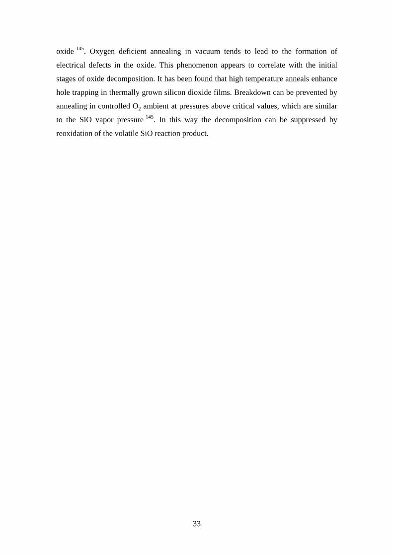
33
oxide 145. Oxygen deficient annealing in vacuum tends to lead to the formation of
electrical defects in the oxide. This phenomenon appears to correlate with the initial
stages of oxide decomposition. It has been found that high temperature anneals enhance
hole trapping in thermally grown silicon dioxide films. Breakdown can be prevented by
annealing in controlled O2 ambient at pressures above critical values, which are similar
to the SiO vapor pressure 145. In this way the decomposition can be suppressed by
reoxidation of the volatile SiO reaction product.
34
4 Electrical Characterization of Ultrathin Insulators
There are several characterization methods that give information about thin films and
interfaces. The focus here is on electrical characterization, which provides useful
information particularly for the fabrication of electronic devices. Conventional
capacitance-voltage (CV) characterization techniques cannot, however, be used in the
separation of positive and negative trapped-charge densities, as they sense the total
charge, only 64.
The Poisson equation of ideal MOS structure (Figure 2.1) gives the relation between
charge and potential. As mentioned before our samples can be quite far from being
ideal. The non-idealities can, however, be taken into account in the characterization by
separating their effect from the measurements or some of them can also be excluded by
careful measurements and fabrication processes.
One-dimensional equations can be used as valid approximation when the area of the
MOS structure is large compared to the thickness of the insulator. Then
[ ]d V
dz
dE
dz
qN z N z n z p z
SiA D
2
2= − = − + −− +
ε( ) ( ) ( ) ( ) ,
(4.1)
where, εSi is the dielectric constant of the silicon, q is unit charge, n is electron and p
hole density, z is position co-ordinate perpendicular to the interface, and NA− and ND
+
are the densities of the ionized acceptor and donor atoms. V and E denote the potential
and electric field.
From equation (4.1), when the potential and electric field far from the silicon/silicon
dioxide -interface are defined as zero, a relation can be derived for electric field 46:
( ) ( )[ ]ε Si B A DE z k T p z p n z n q N N V z20 02( ) ( ) ( ) ( )= − + − + −− + (4.2)
when
35
kTqVkTVq epzpenzn −≈∧≈ 00 )( )( (4.3)
and n0 and p0 are the carrier concentrations in thermal equilibrium, far from the
interface. Then at the silicon/silicon dioxide -interface
[ ]V V zkT
q N Np p V n n V
q N NEs
A Ds s
Si
A Ds= = =
−− + − +
−− + − +( )( )
( ) ( )( )
020 0
2ε .
(4.4)
If there is no charge in the oxide, the surface field in the silicon is
( )ox
sfbg
Si
ox
Si
oxs d
VVVzEzEE
−−εε
=−=εε
=+== )0()0( .(4.5)
In this equation Vg is the gate voltage (potential on the metal), Vfb is the flat band
voltage and dox is the thickness of the oxide. The bending of the energy bands, and
consequently the charge densities, can be numerically calculated from equations (4.3),
(4.4) and (4.5) 146. It can be seen from Figure 4.1, that the band bending in accumulation
is relatively modest.
-2 -1 0 1 2-0.4
-0.2
0.0
0.2
0.4
0.6
0.8
1.0
Vs
(eV)
Vg - Vfb (V)
Figure 4.1 Potential at the oxide/silicon interface of an MOS structure (NA = 1016cm-3,dox = 2 nm) as a function of gate voltage.

36
4.1 Oxide Charge
The most usual way to define the density of a fixed charge in the insulator layer is to
calculate it on the basis of the flat-band voltage shift.
If the insulator is charged, then the electric field will not stay constant, like assumed in
equation (4.5). If it is assumed that there exists a Dirac delta function (δ) like interface
charge (Ns) in the silicon/silicon dioxide interface and that otherwise the charge density
in the insulator is uniform (Nox), then the Poisson equation (4.1) in the oxide is
(structure like in Figure 2.1)
[ ] [ ]0, , )0()(
2
2
oxsoxox
dzNNq
dz
Vd
dz
zdE −∈δ+ε
=−= .(4.6)
Then the electric field in oxide is
[ ] [ ]E zq
N z N E z dox
ox sSi
oxox( ) ( ), ,= + + + ∈ −
εεε
0 0 (4.7)
and potential
[ ]V zq
N z N z E z V z dox
ox sSi
oxs ox( ) ( ) , ,= − +
− + + ∈ −ε
εε
1
20 02 .
(4.8)
In the metal/oxide interface the potential is defined by the gate potential
V d V Vq
Ek T
N
nox g fb Met Sig
BA
i
( ) ln− = − − − − −
∆ Φ Φ1
2
(4.9)
for p-doped and
37
V d V Vq
Ek T
N
nox g fb Met Sig
BD
i
( ) ln− = − − − − +
∆ Φ Φ1
2
(4.10)
for n-doped silicon. ni is intrinsic carrier concentration, ΦMet is the work function of
metal and ΦSi the work function of silicon. Eg is the width of the energy gap and
V V Vfb fb bi= +∆ , (4.11)
in which the Vbi is flat band voltage in an ideal MOS structure. The shift in the gate
potential caused by the oxide and interface charge is
+
ε−=−∆ oxsoxox
oxox dNdN
qdV 2
2
1)( ,
(4.12)
and therefore the relation between the flat band shift and the charge in the oxide and
silicon/silicon dioxide interface is
ox
fboxoxoxs qd
VdNN
∆ε−=+
2
1 .
(4.13)
4.2 Impedance of Thin Oxide MOS Structure
It is extremely difficult to produce reliable measurements when the measured oxide is
very thin. It has been observed, for instance 147, that in MOS structures, the gate
capacitance is typically less than 90% of the ‘traditional’ oxide capacitance, and for
ultra thin oxide layers and relatively low doped polysilicon gates (< 1020 cm-3) it can
even drop below 75%. For thin oxides then, the effective electrical thickness exceeds
the physical thickness of the layer. This means that the established measurement
techniques and analyses used in more traditional MOS characterization are not
necessarily valid any more. It follows that the traditional formulas need to be developed
if we intend to achieve better reliability in MOS characterization.
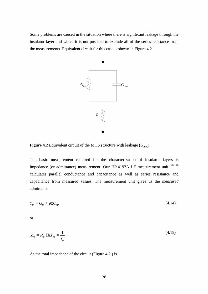
38
Some problems are caused in the situation where there is significant leakage through the
insulator layer and where it is not possible to exclude all of the series resistance from
the measurements. Equivalent circuit for this case is shown in Figure 4.2 .
Gmos Cmos
Rs
Figure 4.2 Equivalent circuit of the MOS structure with leakage (Gmos).
The basic measurement required for the characterization of insulator layers is
impedance (or admittance) measurement. Our HP 4192A LF measurement unit 148,149
calculates parallel conductance and capacitance as well as series resistance and
capacitance from measured values. The measurement unit gives us the measured
admittance
Ym = Gm + iωCm, (4.14)
or
Z R iXYm m m
m
= + = 1 .
(4.15)
As the total impedance of the circuit (Figure 4.2 ) is
39
Z RG i C Ys
mos mos
= ++
=1 1
ω ,
(4.16)
it follows that when this is assumed to be equal with the measured values
−
ω=
−11
Imag1
sm
mos RY
C .(4.17)
or
( ) ( )C
C
R G R Cmos
m
s m s m
=− +1
2 2ω ,
(4.18)
It is, however, hard to define the real value of series resistance. If it is assumed that
Gmos = 0 (i.e. there is no leakage), then
( )R G
G
G Cs mos
m
m m
( )= =+
02 2ω
(4.19)
and
mmosmos X
GCω
−== 1)0( .
(4.20)
The main difficulty in characterization is presented by combining series resistance and
leakage current. If the leakage current is low, equation (4.20) gives quite a good
approximation of real oxide capacitance. If the leakage is high, then the real value of the
capacitance is closer to the admittance measurement (equation (4.14), example in Figure
4.3). Then it is not possible to calculate exact values for layer capacitance, but only
upper and lower limits.
Series resistance is usually taken into account by giving it a constant value. This is
calculated from the measured accumulation capacitance and conductance based on
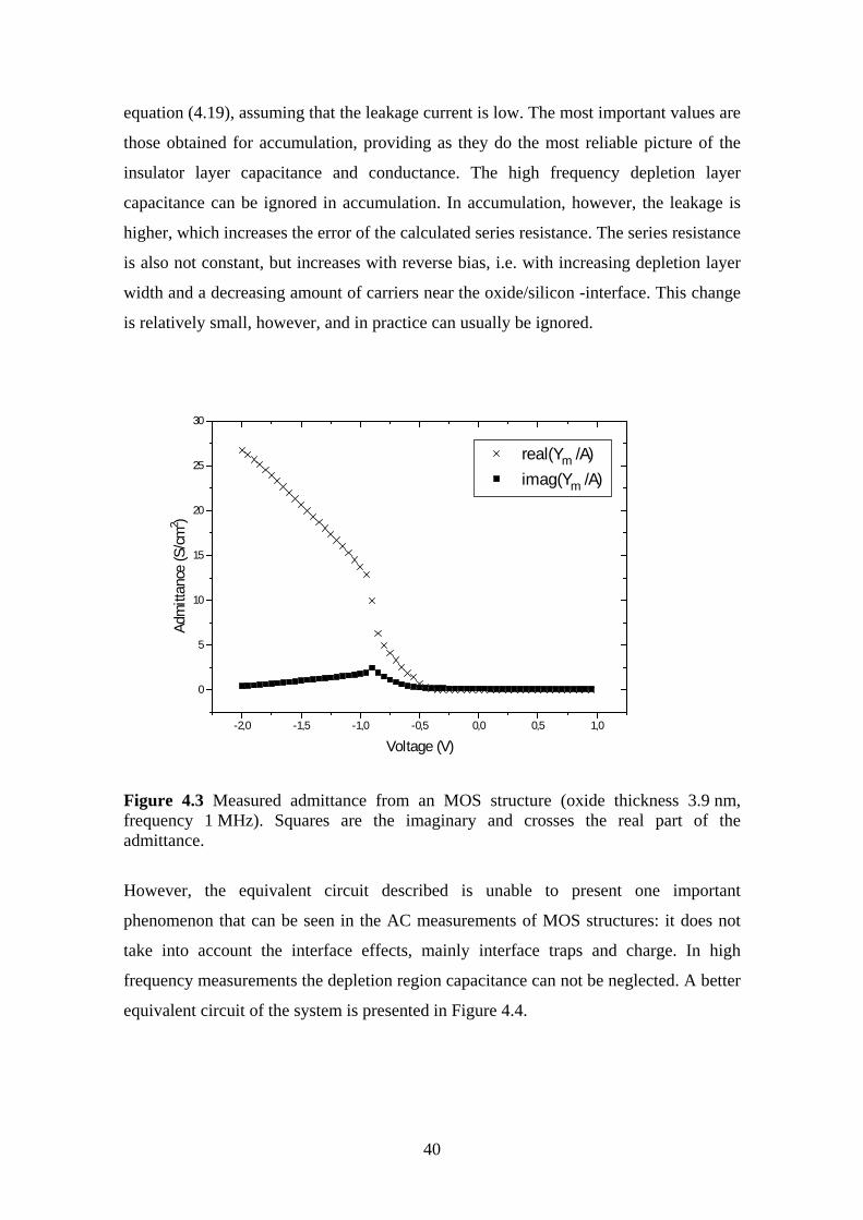
40
equation (4.19), assuming that the leakage current is low. The most important values are
those obtained for accumulation, providing as they do the most reliable picture of the
insulator layer capacitance and conductance. The high frequency depletion layer
capacitance can be ignored in accumulation. In accumulation, however, the leakage is
higher, which increases the error of the calculated series resistance. The series resistance
is also not constant, but increases with reverse bias, i.e. with increasing depletion layer
width and a decreasing amount of carriers near the oxide/silicon -interface. This change
is relatively small, however, and in practice can usually be ignored.
-2,0 -1,5 -1,0 -0,5 0,0 0,5 1,0
0
5
10
15
20
25
30
real(Ym /A)
imag(Ym /A)
Adm
ittan
ce (S
/cm
2 )
Voltage (V)
Figure 4.3 Measured admittance from an MOS structure (oxide thickness 3.9 nm,frequency 1 MHz). Squares are the imaginary and crosses the real part of theadmittance.
However, the equivalent circuit described is unable to present one important
phenomenon that can be seen in the AC measurements of MOS structures: it does not
take into account the interface effects, mainly interface traps and charge. In high
frequency measurements the depletion region capacitance can not be neglected. A better
equivalent circuit of the system is presented in Figure 4.4.
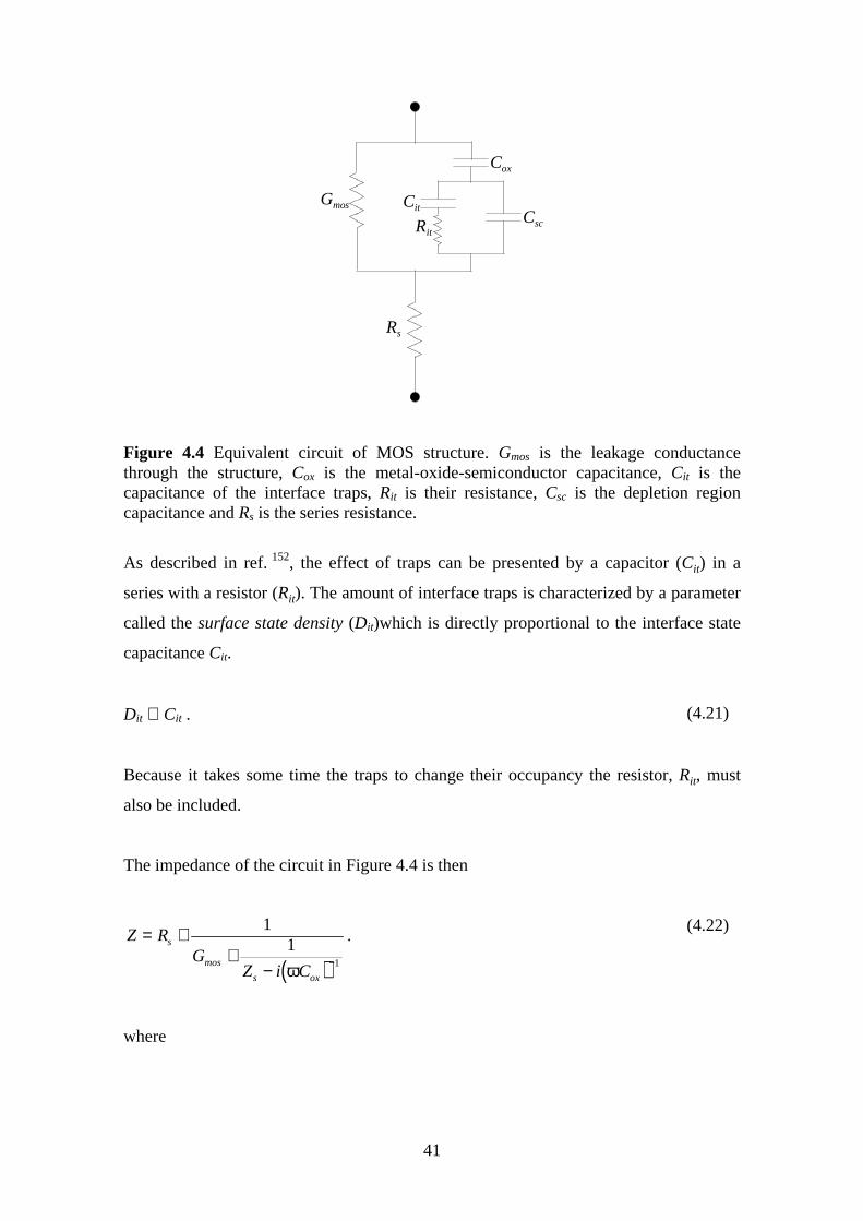
41
Gmos
Cox
Rs
Csc
Cit
Rit
Figure 4.4 Equivalent circuit of MOS structure. Gmos is the leakage conductancethrough the structure, Cox is the metal-oxide-semiconductor capacitance, Cit is thecapacitance of the interface traps, Rit is their resistance, Csc is the depletion regioncapacitance and Rs is the series resistance.
As described in ref. 152, the effect of traps can be presented by a capacitor (Cit) in a
series with a resistor (Rit). The amount of interface traps is characterized by a parameter
called the surface state density (Dit)which is directly proportional to the interface state
capacitance Cit.
Dit ∝ Cit . (4.21)
Because it takes some time the traps to change their occupancy the resistor, Rit, must
also be included.
The impedance of the circuit in Figure 4.4 is then
( )Z R
GZ i C
s
mos
s ox
= ++
− −
11
1ω
.(4.22)
where
42
Z
Z Ri
C
Z
iZ C
s
it itit
it
it sc
== −
+
ω
ω
, in accumulation
, in depletion1
.
(4.23)
The depletion region capacitance Csc is defined by
CA
dscSi
sc
= ε .
(4.24)
The width of the depletion region dsc is usually derived by using the assumption that
there is a region in which all donors and acceptors are ionized and there are no free
carriers. Outside this region there prevails charge neutrality. By using the Poisson
equation (4.1), one gets
dV
q N Nsc
Si s
A D
=−− +
2ε .
(4.25)
A maximum length is usually defined for the depletion region. This is reached when
depletion turns into inversion, i.e. when the density of minority carriers at the interface
exceeds the majority doping concentration
( )+−
+−
−
−
=DA
i
DABSi
scNNq
n
NNTk
d2
ln4
max
ε .
(4.26)
4.3 Oxide Thickness
The basic formula for the calculation of oxide thickness from an MOS structure can be
derived from equation (4.5). On this basis, the ideal differential low frequency
capacitance of an ideal MOS structure is
43
CdQ
dVA
d E
dV
A
d
dV
dV
A
ddV
dEg
Si s
g
ox
ox
s
g
ox
oxox
Si
s
s
= = = −
=
+
ε ε εεε
1 ,(4.27)
where A is the area of the capacitor. By using equations (4.4), (4.5) and (4.27) it is
possible to derive the capacitance formula even further:
CA
dE
q N N p n
ox
oxox s
D A s s
=+
− − +
εε
( )
.(4.28)
Based on equation (4.27), the oxide thickness is 150
dA
C
dV
dEox oxSi
s
s
= −
ε
ε1
.(4.29)
When the MOS structure is biased into accumulation Vs should saturate, and
consequently its derivative should approach zero. This can also be seen from equation
(4.28), as the density of the surface majority carrier increases exponentially with the
surface potential, faster than the surface field (equation (4.5)). Then we get the familiar
equation for the relation between capacitance and insulator thickness:
CA
dacc oxox
≈ ε .(4.30)
Cacc is the saturated accumulation capacitance of the MOS structure.
The first problem is how to define the real oxide capacitance. First of all, the series
resistance does not remain constant even during one measurement, because the bias
voltage affects the depth of the depletion layer and the interface charge. For the
measurement of thickness, the accumulation capacitance is more important. The
problem is that the leakage current peaks in accumulation, thus increasing the error in
series resistance given by equation (4.19). More reliable values can be obtained by
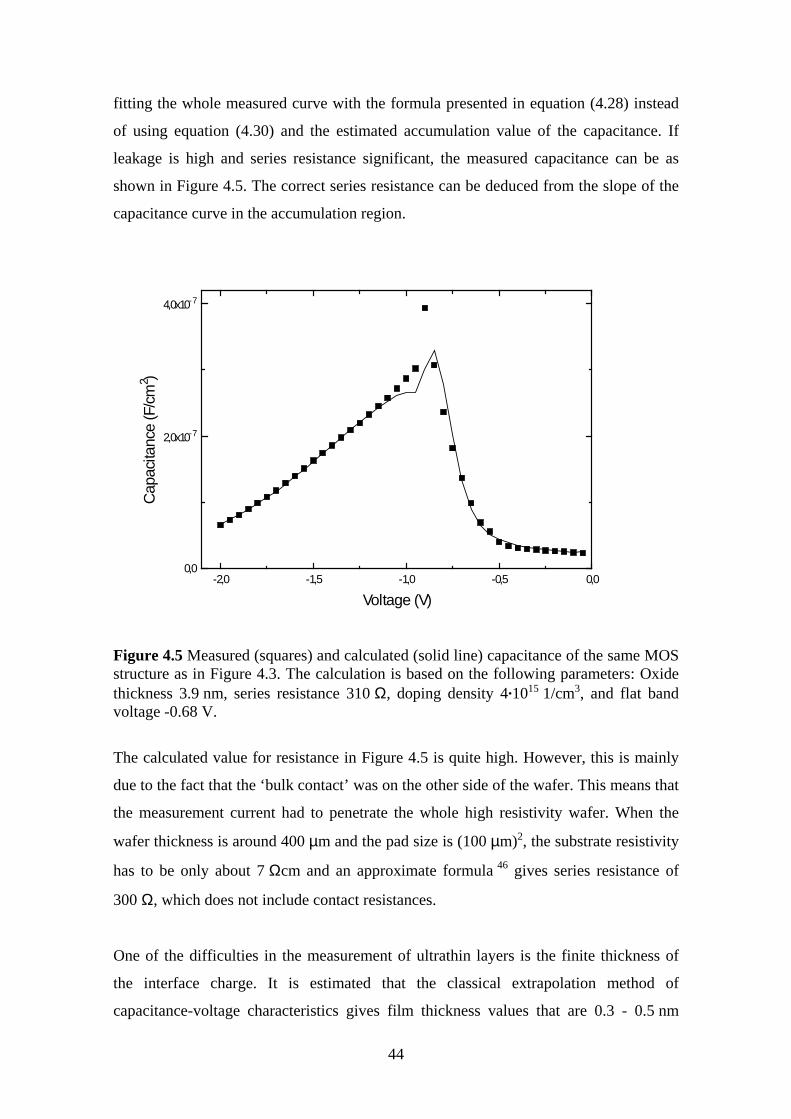
44
fitting the whole measured curve with the formula presented in equation (4.28) instead
of using equation (4.30) and the estimated accumulation value of the capacitance. If
leakage is high and series resistance significant, the measured capacitance can be as
shown in Figure 4.5. The correct series resistance can be deduced from the slope of the
capacitance curve in the accumulation region.
-2,0 -1,5 -1,0 -0,5 0,00,0
2,0x10⁻⁷
4,0x10⁻⁷
Cap
acita
nce
(F/c
m2 )
Voltage (V)
Figure 4.5 Measured (squares) and calculated (solid line) capacitance of the same MOSstructure as in Figure 4.3. The calculation is based on the following parameters: Oxidethickness 3.9 nm, series resistance 310 Ω, doping density 4.1015 1/cm3, and flat bandvoltage -0.68 V.
The calculated value for resistance in Figure 4.5 is quite high. However, this is mainly
due to the fact that the ‘bulk contact’ was on the other side of the wafer. This means that
the measurement current had to penetrate the whole high resistivity wafer. When the
wafer thickness is around 400 µm and the pad size is (100 µm)2, the substrate resistivity
has to be only about 7 Ωcm and an approximate formula 46 gives series resistance of
300 Ω, which does not include contact resistances.
One of the difficulties in the measurement of ultrathin layers is the finite thickness of
the interface charge. It is estimated that the classical extrapolation method of
capacitance-voltage characteristics gives film thickness values that are 0.3 - 0.5 nm
45
larger than those produced by quantum mechanical analysis of the structure 15. The main
reason for this is said to be that in quantum capacitance calculations, the inversion
charge has to be calculated on the basis of the wave functions of every sub-band
forming into the interface when the energy bands are bended. For this reason the oxide
thickness given by equation (4.30) is really the average distance of the accumulation
charge in silicon from the interface charge between the oxide and the metal. Since the
accumulation capacitance also does not totally saturate when the bias increases, it seems
that the oxide layer becomes thinner in direct proportion to increasing voltage. Equation
(4.28) takes this into account, which means that this effect can be avoided by numerical
fitting of admittance measurements.
4.4 Surface State Density
Surface state density is a very important factor in MOSFET structures, since the current
flows along the silicon/silicon dioxide interface. If the density is too high, MOSFETs
will not work at all. The problem can not be avoided entirely, but in a good MOS
process it is possible to achieve state densities around 1010 eV-1cm-2.
The capacitance caused by interface traps (Cit) can be calculated on the basis of the
equivalent circuit presented in Figure 4.4. For the forward biased, i.e. accumulation,
case
11
Imag
11
−
−
−ω
=−−
mossox
oxit
GRY
C
CC ,
(4.31)
and for the reverse biased depletion case
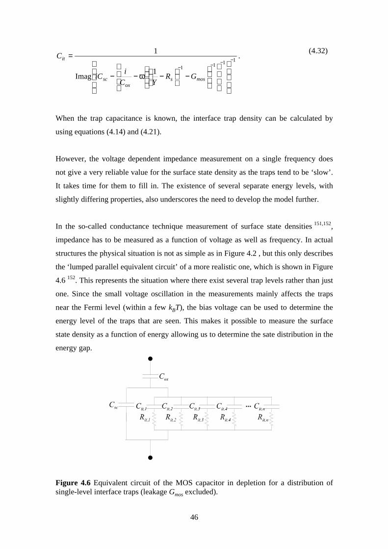
46
11111
Imag
1−−−−
−
−ω−−
=
mossox
sc
it
GRYC
iiC
C .(4.32)
When the trap capacitance is known, the interface trap density can be calculated by
using equations (4.14) and (4.21).
However, the voltage dependent impedance measurement on a single frequency does
not give a very reliable value for the surface state density as the traps tend to be ‘slow’.
It takes time for them to fill in. The existence of several separate energy levels, with
slightly differing properties, also underscores the need to develop the model further.
In the so-called conductance technique measurement of surface state densities 151,152,
impedance has to be measured as a function of voltage as well as frequency. In actual
structures the physical situation is not as simple as in Figure 4.2 , but this only describes
the ‘lumped parallel equivalent circuit’ of a more realistic one, which is shown in Figure
4.6 152. This represents the situation where there exist several trap levels rather than just
one. Since the small voltage oscillation in the measurements mainly affects the traps
near the Fermi level (within a few kBT), the bias voltage can be used to determine the
energy level of the traps that are seen. This makes it possible to measure the surface
state density as a function of energy allowing us to determine the sate distribution in the
energy gap.
Figure 4.6 Equivalent circuit of the MOS capacitor in depletion for a distribution ofsingle-level interface traps (leakage Gmos excluded).

47
The surface state density at a defined energy level can be calculated by using the
relation 152
( )D
q Af
Yit b
it= 12
Real ( )
max
ωω
,(4.33)
where A is capacitor area, fb is material dependent parameter, and
( )[ ] ( )Y
Z R G i Cit
s mos ox
=− − +− − −
11 1 1ω
(4.34)
Figure 4.7 A schematic illustration of trap conductance as a function of angularfrequency.
The state potential that corresponds to a given bias voltage is
++
−
++
+
=torsemiconduc doped-nfor , )(ln
2
torsemiconduc doped-pfor , )(ln2
q
EVV
n
N
q
kT
q
E
q
EVV
n
N
q
kT
q
E
Vv
gsi
Dg
vgs
i
Ag
trap ,
(4.35)
where Eg is the semiconductor energy bandgap and interface potential Vs like in
equation (4.4).
48
This model is quite commonly used. However, it has been criticized for not including
so-called ‘slow traps’, as there is some evidence that there are two populations of
defects at the silicon/silicon dioxide interface 20. The measurements are also time-
consuming because the admittance has to be measured as a function of both voltage and
frequency. This was nonetheless the method I decided to use in an attempt to get a more
reliable picture of the state densities in the gap as a function of energy.
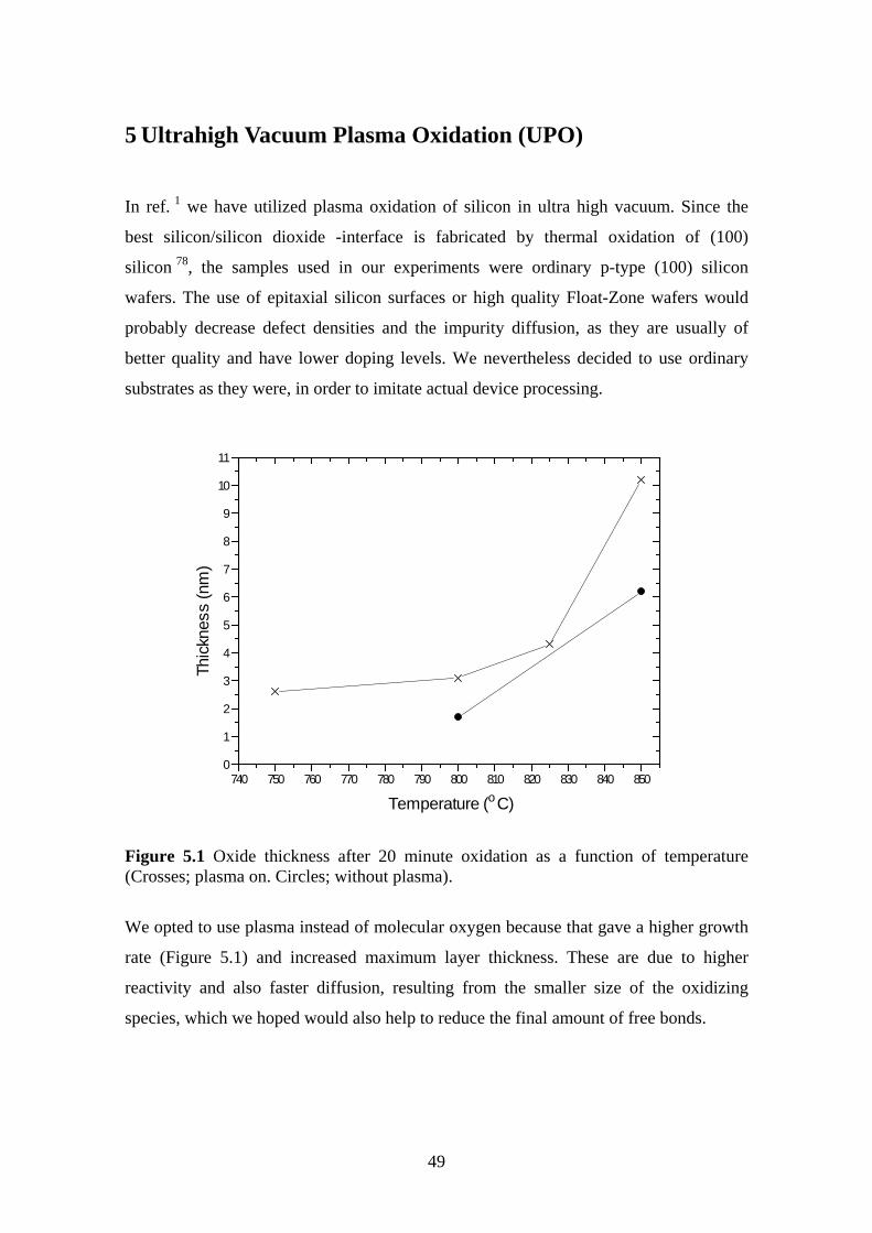
49
5 Ultrahigh Vacuum Plasma Oxidation (UPO)
In ref. 1 we have utilized plasma oxidation of silicon in ultra high vacuum. Since the
best silicon/silicon dioxide -interface is fabricated by thermal oxidation of (100)
silicon 78, the samples used in our experiments were ordinary p-type (100) silicon
wafers. The use of epitaxial silicon surfaces or high quality Float-Zone wafers would
probably decrease defect densities and the impurity diffusion, as they are usually of
better quality and have lower doping levels. We nevertheless decided to use ordinary
substrates as they were, in order to imitate actual device processing.
740 750 760 770 780 790 800 810 820 830 840 8500
1
2
3
4
5
6
7
8
9
10
11
Thic
knes
s (n
m)
Temperature (oC)
Figure 5.1 Oxide thickness after 20 minute oxidation as a function of temperature(Crosses; plasma on. Circles; without plasma).
We opted to use plasma instead of molecular oxygen because that gave a higher growth
rate (Figure 5.1) and increased maximum layer thickness. These are due to higher
reactivity and also faster diffusion, resulting from the smaller size of the oxidizing
species, which we hoped would also help to reduce the final amount of free bonds.
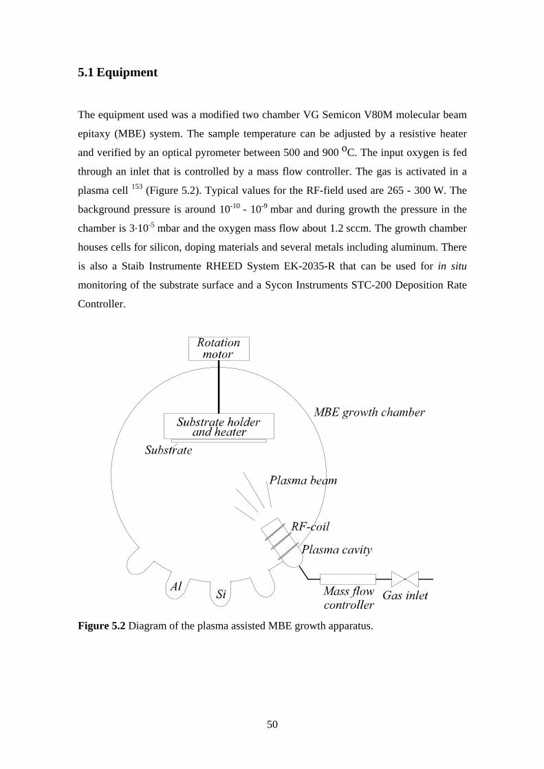
50
5.1 Equipment
The equipment used was a modified two chamber VG Semicon V80M molecular beam
epitaxy (MBE) system. The sample temperature can be adjusted by a resistive heater
and verified by an optical pyrometer between 500 and 900 oC. The input oxygen is fed
through an inlet that is controlled by a mass flow controller. The gas is activated in a
plasma cell 153 (Figure 5.2). Typical values for the RF-field used are 265 - 300 W. The
background pressure is around 10-10 - 10-9 mbar and during growth the pressure in the
chamber is 3.10-5 mbar and the oxygen mass flow about 1.2 sccm. The growth chamber
houses cells for silicon, doping materials and several metals including aluminum. There
is also a Staib Instrumente RHEED System EK-2035-R that can be used for in situ
monitoring of the substrate surface and a Sycon Instruments STC-200 Deposition Rate
Controller.
Figure 5.2 Diagram of the plasma assisted MBE growth apparatus.
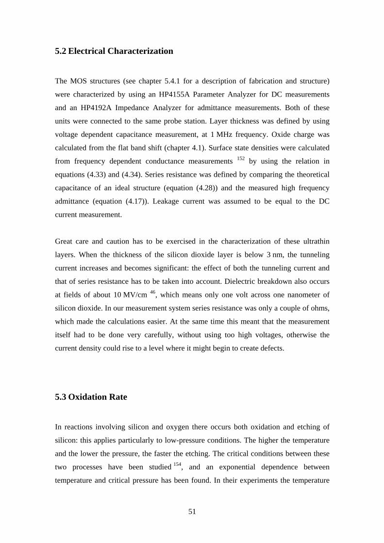
51
5.2 Electrical Characterization
The MOS structures (see chapter 5.4.1 for a description of fabrication and structure)
were characterized by using an HP4155A Parameter Analyzer for DC measurements
and an HP4192A Impedance Analyzer for admittance measurements. Both of these
units were connected to the same probe station. Layer thickness was defined by using
voltage dependent capacitance measurement, at 1 MHz frequency. Oxide charge was
calculated from the flat band shift (chapter 4.1). Surface state densities were calculated
from frequency dependent conductance measurements 152 by using the relation in
equations (4.33) and (4.34). Series resistance was defined by comparing the theoretical
capacitance of an ideal structure (equation (4.28)) and the measured high frequency
admittance (equation (4.17)). Leakage current was assumed to be equal to the DC
current measurement.
Great care and caution has to be exercised in the characterization of these ultrathin
layers. When the thickness of the silicon dioxide layer is below 3 nm, the tunneling
current increases and becomes significant: the effect of both the tunneling current and
that of series resistance has to be taken into account. Dielectric breakdown also occurs
at fields of about 10 MV/cm 46, which means only one volt across one nanometer of
silicon dioxide. In our measurement system series resistance was only a couple of ohms,
which made the calculations easier. At the same time this meant that the measurement
itself had to be done very carefully, without using too high voltages, otherwise the
current density could rise to a level where it might begin to create defects.
5.3 Oxidation Rate
In reactions involving silicon and oxygen there occurs both oxidation and etching of
silicon: this applies particularly to low-pressure conditions. The higher the temperature
and the lower the pressure, the faster the etching. The critical conditions between these
two processes have been studied 154, and an exponential dependence between
temperature and critical pressure has been found. In their experiments the temperature
52
was between 890 and 1150 oC and pressure from 0.07 to 70 mbar. It was noted that
etching and growth rates were equal when the pressure is
P T P ecrE kTA( ) = −
0 . (5.1)
where P0 = 5.9.1012 bar and EA = 3.83 eV. These parameters seemed to be independent
of silicon doping and surface crystal orientation 155.
However, this formula was tested in a different temperature and pressure range than we
are using, which means it cannot be used as such. The best way to find the proper
process parameters is by way of experimentation.
5.3.1 Experiment
The samples used in the oxidation rate determination 1 were ordinary p-type (100)
silicon wafers, with a resistivity of about 10 Ωcm. These were cleaned using a standard
chemical cleaning process (5 minute ultrasonic in acetone and isopropyl alcohol, 10
minutes in H2O:NH4OH:H2O2 (5:1:1) at 80 oC, 10 minutes in H2O:HCl:H2O2 (5:1:1) at
80 oC). The native oxide was removed in situ in the MBE UHV chamber by keeping the
samples at 875 oC for 15 minutes. The surface was monitored by RHEED to check that
the oxide had been fully removed.
During oxidation the substrate temperature was between 600 and 850 oC as determined
by an optical pyrometer. The growth times varied from 20 to 30 minutes. In all our
experiments the oxygen flow was about 1.3 sccm. The background pressure was around
10-8 mbar, and during growth the pressure in the chamber was 2.5.10-5 mbar.
The oxide thicknesses were measured by an ellipsometer using the fixed value of the
refractive index n = 1.465, typical of silicon dioxide (wavelength 632.8 nm). All the
results are averaged from ten measurements, which varied by less than about 0.1 nm. It
is known, however, that the refractive index of very thin silicon dioxide films differs
from the value of thicker layers 33, which may give rise to inaccuracies. Also, the
53
manufacturer of the ellipsometer does not guarantee the accuracy of the results below
1 nm. The ellipsometric measurements were, however, compared with results from
capacitance measurements as well as tunneling current measurements 156 and were
found to be in close agreement (differences within 0.1 nm, the film thicknesses being 2 -
3 nm).
0 5 10 15 20 25 300
2
4
6
8
10
12Calculated:
600 o C
700 o C
800 o CMeasured:
600 o C
700 o C
800 o C
Thi
ckne
ss (
nm)
Time (min)
Figure 5.3 Measured thickness of the silicon dioxide layer as a function of time atvarious temperatures 1 . The calculations are based on equations (5.3) and (5.4) whichare fitted with the measurements.
As we can see in Figure 5.3, the average growth rate is very slow for the first 15
minutes, less than 0.1 nm/min 1. It then increases very sharply, reaching about 1 nm/min
at 800 oC. This indicates that the sticking coefficient of oxygen molecules is smaller on
a pure silicon surface than it is on a silicon dioxide surface, like in ref. 157. This
contradicts the models presented in chapter 3.2.1. This behavior has been seen also in
some other thermal oxidation experiments 158. We observed an incubation period at the
onset of the oxidation procedure at temperatures from room temperature through to
1000 oC. Initially, there were no signs at all of any oxidation, but it only started after a
certain period of time. The duration of this interval seemed to decrease with increasing
temperature, and is supposed that it is sensitive to the nature of surface termination and
the presence of contamination. Growth behavior is therefore not as simple and
54
straightforward as described by equation (3.8). There may be considerable variation in
initial growth, depending on the surface quality. We model this process using only one
parameter, i.e. effective sticking coefficient, to describe all the surface effects and
reactions 1.
Since the sticking coefficients of oxygen are presumably different for silicon and silicon
dioxide surfaces, the oxygen surface concentrations CSi and COx also differ from each
other. When the oxygen flux starts to ‘see’ the surface as a pure silicon dioxide surface,
the critical thickness dcr has been reached and C0 → COx. Below critical thickness, we
simply interpolate for the average surface concentration. Thus we obtain 1
CC
C C
dz d
C z d
SiOx Si
crcr
Ox cr
0 =+
−<
≥
,
,
when
when
.(5.2)
Solving equations (3.1) - (3.4) and (5.2), we get
[ ]t
d
B rz
A rd
r r
z
dz d
Bz d A z d z d
cr
crcr
cr cr cr
= −+ −
−
+ −
<
− + − + ≥
2
1 2 11
11
1 2 2
( )ln ,
( ) ,
when
when τ
,
(5.3)
where
−−−
−==τ )ln(
12)1(
2)( r
r
rdAd
rB
ddt cr
crcr
cr .(5.4)
The parameter
r = CSi/COx , (5.5)
is called the relative sticking coefficient. If r < 1, what it seems to be for good quality
silicon surfaces, the initial growth rate is slow but increases to its maximum when the
55
thickness reaches around 1 nm 1.
The initial growth rate should decrease with increasing temperature 159. Because the
linear rate constant tends to increase with temperature 46, the relative sticking coefficient
has to decrease even faster. From equations (5.3) and (5.4), it can be derived that
dz
dt
B
Ar
t =
=0
.(5.6)
The value of r is approximately the same as the ratio between the initial growth rate and
the growth rate after z > dcr , as
dz
dt
B
A dt cr=
=+τ 2
.(5.7)
The decrease in r with increasing temperature can be derived then from a comparison of
these growth rates at different temperatures. This means that the relative sticking
coefficient r is much lower than 1. It is a difficult task to measure the initial growth
behavior, but our results suggest it is also possible that r could even reach values over
one at lower temperatures. In other words the sticking probability would be higher on
silicon than on silicon dioxide surfaces 1 and should increase with decreasing
temperature.
Our measurements 1 indicate that the critical thickness dcr is about 1 nm for our samples
when the oxidation temperature is over 700 oC, and seems to increase slowly with
declining temperature. This can be interpreted to mean that the average layer thickness
increases at the moment when the entire sample surface is finally covered with dioxide.
This implies a deterioration of layer quality. If the growth starts from separate spots and
continues in a island form until they unite, it can be assumed that bigger the dcr is,
higher the islands get. Consequently there is more roughness. Another possible
explanation is that at the lower temperatures, the initial layer quality is in some other
way so poor that the reactions differ from those which are happening on high quality
silicon dioxide surface. A thicker layer is needed before the reactions begin to
approximate those occurring on silicon dioxide surfaces.
56
As can be seen in Figure 5.4, the growth rate is closely dependent on temperature. For
maximum thickness control, it is better to use lower temperatures, because otherwise the
growth rate, when the critical thickness is exceeded, will increase too much.
600 650 700 750 800 8500
2
4
6
8
10
12 20 min 30 min
Thi
ckne
ss (n
m)
Temperature (oC)
Figure 5.4 Thickness of the silicon dioxide layer as a function of temperature after 20and 30 minutes of processing 1.
Figure 5.5 shows a typical thickness profile of a silicon dioxide layer. The
measurements were taken in four directions from the center. The thickness seems to be
more or less uniform, which means that the processing parameters and conditions used
are about right. The processing temperature does not seem to have any significant effect
on thickness uniformity. The minor variations in thickness can be partly explained by
the fact that in the MBE, the molecule flux is bigger in the center of the beam. There is,
however, considerable variation in the results from different wafers, which can be
explained by temperature changes on the wafer. Owing to the structure of the resistive
heating element and the sample holder, the temperature is usually somewhat higher in
the center of the wafer, and the same goes for growth velocity. The condition of the
heating element is, however, crucially important: when it starts to corrode before
reaching breaking point, part of the film will be clearly thinner because the sample will
not be evenly heated (Figure 5.6).
57
0.0 0.5 1.0 1.5 2.0 2.5 3.00.0
0.2
0.4
0.6
0.8
1.0
1.2
1.4
1.6
1.8
Thi
ckne
ss (
nm)
Distance from the centre (cm)
Figure 5.5 Thickness profile of a silicon dioxide layer processed at 750 oC for 30minutes. The solid line is averaged from the measured values from four directions fromthe center. The measurements are presented as squares. 1
0.0 0.5 1.0 1.5 2.0 2.5 3.00
2
4
6
8
10
Thi
ckne
ss (
nm)
Distance from the centre (cm)
Figure 5.6 Thickness profile of a silicon dioxide layer in four directions from thecenter. The sample was processed at 800 oC for 30 minutes with a corroded heatingelement. 1
58
5.4 Room Temperature Oxidation
As has been pointed out earlier, higher processing temperatures produce better quality
silicon dioxide layers. However, in a UHV system it is not possible to use very high
temperatures, because otherwise the desorption rate may exceed the oxidation rate.
Equipment limitations also restrict the temperatures available at below 900 oC. In our
experiments 1 we have noticed that below 700 oC, oxidation almost saturates after only
a few nanometers. This means that the useful process window is quite narrow. To
resolve this problem we have tried a completely opposite approach, i.e. oxidation at
room temperature, which is a more ‘gentle’ process. TEM measurements (Figure 5.7)
indicate that the process we are introducing seems to produce an extremely flat interface
and homogenous layer thickness 12.
Figure 5.7 TEM picture of a silicon/silicon dioxide heterostructure.
59
5.4.1 Experiment
Three-inch boron doped (100) silicon wafers (NA = 0.5 - 1.1016 cm-3) were used as
substrates. These were thermally dry oxidized at 1000 oC to form a 100-nm thick
insulator layer. 100 µm x 100 µm openings were etched using photolithography and
buffered HF. After an HF dip, samples were inserted in the MBE system, and the
sample temperature was raised to 780 oC. A low silicon flux was then used to etch the
native oxide layer off from the openings. The temperature used has been reported to be
the lowest possible for purposes of producing an atomically flat surface 73. Oxide
removal was verified by monitoring the surface by RHEED. The temperature was then
allowed to drop to room temperature. The actual oxidation was performed by feeding
pure oxygen gas through a plasma cell in which the RF power was 265 W. The pressure
in the chamber during oxidation was 3.10-5 mbar, and the oxygen mass flow was
1.2 sccm.
In our experiments 12 we have found that the maximum layer thickness that can be
reached at room temperature is 1 - 1.1 nm. In order to produce thicker layers, the
procedure we applied was to evaporate a thin, about 0.6 nm, silicon layer on the silicon
dioxide surface and to repeat the oxidation. The silicon layer thickness was defined
using the Sycon Instruments STC-200 Deposition Rate Controller. Each processing
cycle increased the layer thickness by one nanometer. We used 10 minutes for one
oxidation cycle to make sure that all of the vaporized silicon had been oxidized. Once
the desired thickness had been achieved, an aluminum layer of about 100 nm was
vaporized on top of the sample. No post oxidation thermal treatments were used. After
removal from the vacuum chamber, the test structures were patterned by using
photolithography and wet chemical etching (Figure 5.8). The bulk contacts were made
by using GaIn eutect, so that no sintering was needed. The MOS structures (capacitor
area (100 µm)2) were then characterized 152 as described earlier in chapter 5.2.
The method was used to produce two to five nanometer thick silicon dioxide layers. As
can be seen in Figure 5.9, the measured and the expected values are reasonably close to
one another 2. After two oxidation cycles, the measured values varied from 2.0 to
2.2 nm (calculated error is 0.3 nm, mainly due to the leakage current), after three cycles
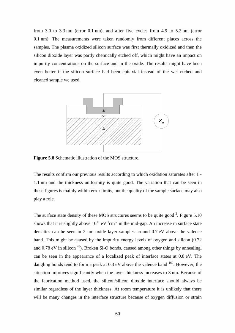
60
from 3.0 to 3.3 nm (error 0.1 nm), and after five cycles from 4.9 to 5.2 nm (error
0.1 nm). The measurements were taken randomly from different places across the
samples. The plasma oxidized silicon surface was first thermally oxidized and then the
silicon dioxide layer was partly chemically etched off, which might have an impact on
impurity concentrations on the surface and in the oxide. The results might have been
even better if the silicon surface had been epitaxial instead of the wet etched and
cleaned sample we used.
Figure 5.8 Schematic illustration of the MOS structure.
The results confirm our previous results according to which oxidation saturates after 1 -
1.1 nm and the thickness uniformity is quite good. The variation that can be seen in
these figures is mainly within error limits, but the quality of the sample surface may also
play a role.
The surface state density of these MOS structures seems to be quite good 2. Figure 5.10
shows that it is slightly above 1011 eV-1cm-2 in the mid-gap. An increase in surface state
densities can be seen in 2 nm oxide layer samples around 0.7 eV above the valence
band. This might be caused by the impurity energy levels of oxygen and silicon (0.72
and 0.78 eV in silicon 46). Broken Si-O bonds, caused among other things by annealing,
can be seen in the appearance of a localized peak of interface states at 0.8 eV. The
dangling bonds tend to form a peak at 0.3 eV above the valence band 160. However, the
situation improves significantly when the layer thickness increases to 3 nm. Because of
the fabrication method used, the silicon/silicon dioxide interface should always be
similar regardless of the layer thickness. At room temperature it is unlikely that there
will be many changes in the interface structure because of oxygen diffusion or strain
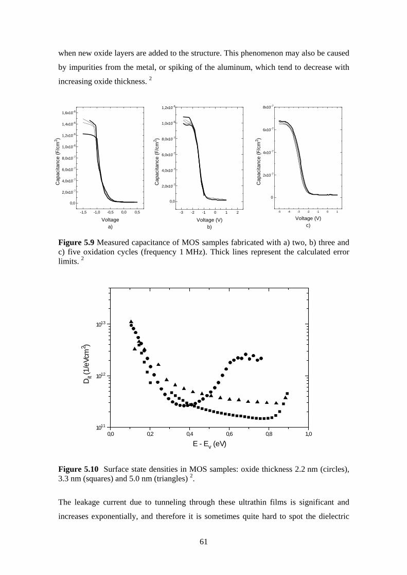
61
when new oxide layers are added to the structure. This phenomenon may also be caused
by impurities from the metal, or spiking of the aluminum, which tend to decrease with
increasing oxide thickness. 2
-1,5 -1,0 -0,5 0,0 0,5
0,0
2,0x10⁻⁷
4,0x10⁻⁷
6,0x10⁻⁷
8,0x10⁻⁷
1,0x10⁻⁶
1,2x10⁻⁶
1,4x10⁻⁶
1,6x10⁻⁶
Cap
acita
nce
(F/c
m2 )
Voltagea)
-3 -2 -1 0 1 2
0,0
2,0x10⁻⁷
4,0x10⁻⁷
6,0x10⁻⁷
8,0x10⁻⁷
1,0x10⁻⁶
1,2x10⁻⁶
Cap
acita
nce
(F/c
m2 )
Voltage (V)b)
-5 -4 -3 -2 -1 0 1
0
2x10⁻⁷
4x10⁻⁷
6x10⁻⁷
8x10⁻⁷
Cap
acita
nce
(F/c
m2 )
Voltage (V)c)
Figure 5.9 Measured capacitance of MOS samples fabricated with a) two, b) three andc) five oxidation cycles (frequency 1 MHz). Thick lines represent the calculated errorlimits. 2
0,0 0,2 0,4 0,6 0,8 1,01011
1012
1013
Dit (
1/eV
cm2 )
E - Ev (eV)
Figure 5.10 Surface state densities in MOS samples: oxide thickness 2.2 nm (circles),3.3 nm (squares) and 5.0 nm (triangles) 2.
The leakage current due to tunneling through these ultrathin films is significant and
increases exponentially, and therefore it is sometimes quite hard to spot the dielectric
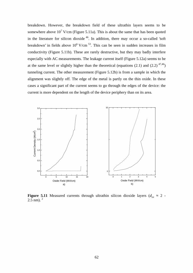
62
breakdown. However, the breakdown field of these ultrathin layers seems to be
somewhere above 107 V/cm (Figure 5.11a). This is about the same that has been quoted
in the literature for silicon dioxide 46. In addition, there may occur a so-called ’soft
breakdown’ in fields above 106 V/cm 53. This can be seen in sudden increases in film
conductivity (Figure 5.11b). These are rarely destructive, but they may badly interfere
especially with AC measurements. The leakage current itself (Figure 5.12a) seems to be
at the same level or slightly higher than the theoretical (equations (2.1) and (2.2) 47,46)
tunneling current. The other measurement (Figure 5.12b) is from a sample in which the
alignment was slightly off. The edge of the metal is partly on the thin oxide. In these
cases a significant part of the current seems to go through the edges of the device: the
current is more dependent on the length of the device periphery than on its area.
0 5 10 15 20
0,0
0,5
1,0
1,5
2,0
2,5
3,0
Cur
rent
Den
sity
(A
/cm
2 )
Oxide Field (MV/cm)a)
0 1 2 3 4 5
0
50
Oxide Field (MV/cm)b)
Figure 5.11 Measured currents through ultrathin silicon dioxide layers (dox ≈ 2 -2.5 nm). 2

63
0 1 2 3 4 510-3
10-2
10-1
100C
urre
nt D
ensi
ty (
A/c
m2 )
Oxide Field (MV/cm)a)
0 1 2 3 4 5
5,0x10⁻⁴
1,0x10⁻³
1,5x10⁻³
2,0x10⁻³
Cur
rent
Den
sity
(A
/cm
2 )
Oxide Field (MV/cm)b)
Figure 5.12 Calculated (solid black line) and measured (dashed red line) tunnelingcurrent through a) 2.2 nm and b) 3 nm ultrathin silicon dioxide layers as a function ofoxide field. 2
5.5 Effect of Oxidation Temperature on the Silicon Dioxide Quality
Given the key impact of temperature on oxide quality, we also studied the effect of
oxidation temperature. The range of temperatures covered was from room temperature
to 800 oC.
5.5.1 Experiment
The substrates were p-type, 10 Ωcm, (100) silicon wafers supplied by Okmetic Ltd.
These were thermally dry oxidized at 1000 oC in order to grow a 100-nm thick insulator
layer. The thermal oxide was patterned using photolithography and buffered HF.
Samples were cleaned using a chemical cleaning process (5 minute ultrasonic in acetone
and isopropyl alcohol, 10 minutes at 80 oC in H2O:NH4OH:H2O2 (5:1:1) and
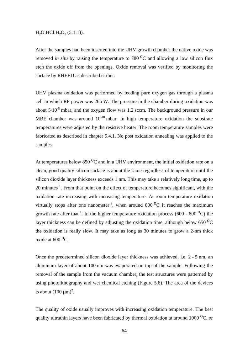
64
H2O:HCl:H2O2 (5:1:1)).
After the samples had been inserted into the UHV growth chamber the native oxide was
removed in situ by raising the temperature to 780 oC and allowing a low silicon flux
etch the oxide off from the openings. Oxide removal was verified by monitoring the
surface by RHEED as described earlier.
UHV plasma oxidation was performed by feeding pure oxygen gas through a plasma
cell in which RF power was 265 W. The pressure in the chamber during oxidation was
about 5.10-5 mbar, and the oxygen flow was 1.2 sccm. The background pressure in our
MBE chamber was around 10-10 mbar. In high temperature oxidation the substrate
temperatures were adjusted by the resistive heater. The room temperature samples were
fabricated as described in chapter 5.4.1. No post oxidation annealing was applied to the
samples.
At temperatures below 850 oC and in a UHV environment, the initial oxidation rate on a
clean, good quality silicon surface is about the same regardless of temperature until the
silicon dioxide layer thickness exceeds 1 nm. This may take a relatively long time, up to
20 minutes 1. From that point on the effect of temperature becomes significant, with the
oxidation rate increasing with increasing temperature. At room temperature oxidation
virtually stops after one nanometer 2, when around 800 oC it reaches the maximum
growth rate after that 1. In the higher temperature oxidation process (600 - 800 oC) the
layer thickness can be defined by adjusting the oxidation time, although below 650 oC
the oxidation is really slow. It may take as long as 30 minutes to grow a 2-nm thick
oxide at 600 oC.
Once the predetermined silicon dioxide layer thickness was achieved, i.e. 2 - 5 nm, an
aluminum layer of about 100 nm was evaporated on top of the sample. Following the
removal of the sample from the vacuum chamber, the test structures were patterned by
using photolithography and wet chemical etching (Figure 5.8). The area of the devices
is about (100 µm)2.
The quality of oxide usually improves with increasing oxidation temperature. The best
quality ultrathin layers have been fabricated by thermal oxidation at around 1000 oC, or
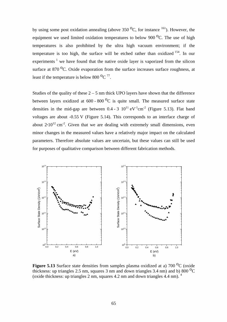
65
by using some post oxidation annealing (above 350 oC, for instance 161). However, the
equipment we used limited oxidation temperatures to below 900 oC. The use of high
temperatures is also prohibited by the ultra high vacuum environment; if the
temperature is too high, the surface will be etched rather than oxidized 154. In our
experiments 1 we have found that the native oxide layer is vaporized from the silicon
surface at 870 oC. Oxide evaporation from the surface increases surface roughness, at
least if the temperature is below 800 oC 77.
Studies of the quality of these 2 – 5 nm thick UPO layers have shown that the difference
between layers oxidized at 600 - 800 oC is quite small. The measured surface state
densities in the mid-gap are between 0.4 - 3 1011 eV-1cm-2 (Figure 5.13). Flat band
voltages are about -0.55 V (Figure 5.14). This corresponds to an interface charge of
about 2.1012 cm-2. Given that we are dealing with extremely small dimensions, even
minor changes in the measured values have a relatively major impact on the calculated
parameters. Therefore absolute values are uncertain, but these values can still be used
for purposes of qualitative comparison between different fabrication methods.
0,0 0,2 0,4 0,6 0,8 1,0109
101 0
101 1
101 2
101 3
101 4
Sur
face
Sta
te D
ensi
ty (
1/eV
cm2 )
E (eV)a)
0,0 0,2 0,4 0,6 0,8 1,0109
101 0
101 1
101 2
101 3
101 4
Sur
face
Sta
te D
ensi
ty (
1/eV
cm2 )
E (eV)b)
Figure 5.13 Surface state densities from samples plasma oxidized at a) 700 oC (oxidethickness: up triangles 2.5 nm, squares 3 nm and down triangles 3.4 nm) and b) 800 oC(oxide thickness: up triangles 2 nm, squares 4.2 nm and down triangles 4.4 nm). 4
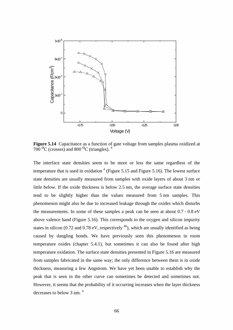
66
-0,75 -0,50 -0,25 0,00
0
3x10⁻⁷
5x10⁻⁷
8x10⁻⁷
1x10⁻⁶
Cap
acita
nce
(F/c
m2 )
Voltage (V)
Figure 5.14 Capacitance as a function of gate voltage from samples plasma oxidized at700 oC (crosses) and 800 oC (triangles). 4
The interface state densities seem to be more or less the same regardless of the
temperature that is used in oxidation 4 (Figure 5.15 and Figure 5.16). The lowest surface
state densities are usually measured from samples with oxide layers of about 3 nm or
little below. If the oxide thickness is below 2.5 nm, the average surface state densities
tend to be slightly higher than the values measured from 5 nm samples. This
phenomenon might also be due to increased leakage through the oxides which disturbs
the measurements. In some of these samples a peak can be seen at about 0.7 - 0.8 eV
above valence band (Figure 5.16). This corresponds to the oxygen and silicon impurity
states in silicon (0.72 and 0.78 eV, respectively 46), which are usually identified as being
caused by dangling bonds. We have previously seen this phenomenon in room
temperature oxides (chapter 5.4.1), but sometimes it can also be found after high
temperature oxidation. The surface state densities presented in Figure 5.16 are measured
from samples fabricated in the same way; the only difference between them is in oxide
thickness, measuring a few Angstrom. We have yet been unable to establish why the
peak that is seen in the other curve can sometimes be detected and sometimes not.
However, it seems that the probability of it occurring increases when the layer thickness
decreases to below 3 nm. 4
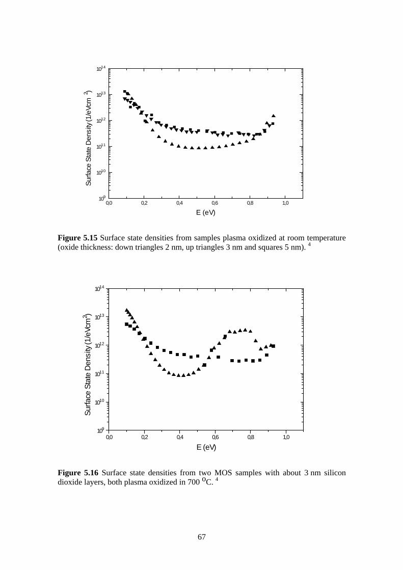
67
0,0 0,2 0,4 0,6 0,8 1,0109
1010
1011
1012
1013
1014
Sur
face
Sta
te D
ensi
ty (1
/eVc
m 2
)
E (eV)
Figure 5.15 Surface state densities from samples plasma oxidized at room temperature(oxide thickness: down triangles 2 nm, up triangles 3 nm and squares 5 nm). 4
0,0 0,2 0,4 0,6 0,8 1,0109
1010
1011
1012
1013
1014
Sur
face
Sta
te D
ensi
ty (1
/eVc
m2 )
E (eV)
Figure 5.16 Surface state densities from two MOS samples with about 3 nm silicondioxide layers, both plasma oxidized in 700 oC. 4
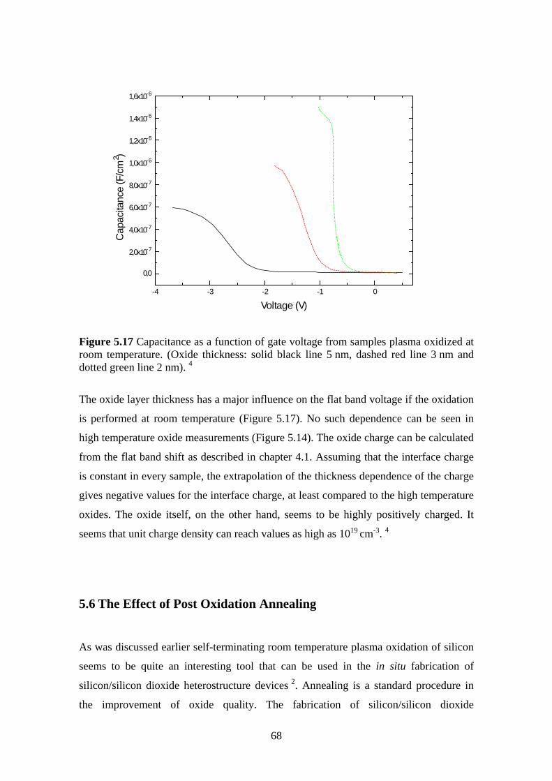
68
-4 -3 -2 -1 0
0,0
2,0x10⁻⁷
4,0x10⁻⁷
6,0x10⁻⁷
8,0x10⁻⁷
1,0x10⁻⁶
1,2x10⁻⁶
1,4x10⁻⁶
1,6x10⁻⁶
Cap
acita
nce
(F/c
m2 )
Voltage (V)
Figure 5.17 Capacitance as a function of gate voltage from samples plasma oxidized atroom temperature. (Oxide thickness: solid black line 5 nm, dashed red line 3 nm anddotted green line 2 nm). 4
The oxide layer thickness has a major influence on the flat band voltage if the oxidation
is performed at room temperature (Figure 5.17). No such dependence can be seen in
high temperature oxide measurements (Figure 5.14). The oxide charge can be calculated
from the flat band shift as described in chapter 4.1. Assuming that the interface charge
is constant in every sample, the extrapolation of the thickness dependence of the charge
gives negative values for the interface charge, at least compared to the high temperature
oxides. The oxide itself, on the other hand, seems to be highly positively charged. It
seems that unit charge density can reach values as high as 1019 cm-3. 4
5.6 The Effect of Post Oxidation Annealing
As was discussed earlier self-terminating room temperature plasma oxidation of silicon
seems to be quite an interesting tool that can be used in the in situ fabrication of
silicon/silicon dioxide heterostructure devices 2. Annealing is a standard procedure in
the improvement of oxide quality. The fabrication of silicon/silicon dioxide
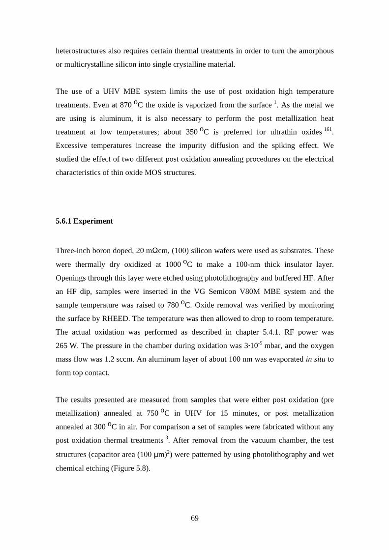
69
heterostructures also requires certain thermal treatments in order to turn the amorphous
or multicrystalline silicon into single crystalline material.
The use of a UHV MBE system limits the use of post oxidation high temperature
treatments. Even at 870 oC the oxide is vaporized from the surface 1. As the metal we
are using is aluminum, it is also necessary to perform the post metallization heat
treatment at low temperatures; about 350 oC is preferred for ultrathin oxides 161.
Excessive temperatures increase the impurity diffusion and the spiking effect. We
studied the effect of two different post oxidation annealing procedures on the electrical
characteristics of thin oxide MOS structures.
5.6.1 Experiment
Three-inch boron doped, 20 mΩcm, (100) silicon wafers were used as substrates. These
were thermally dry oxidized at 1000 oC to make a 100-nm thick insulator layer.
Openings through this layer were etched using photolithography and buffered HF. After
an HF dip, samples were inserted in the VG Semicon V80M MBE system and the
sample temperature was raised to 780 oC. Oxide removal was verified by monitoring
the surface by RHEED. The temperature was then allowed to drop to room temperature.
The actual oxidation was performed as described in chapter 5.4.1. RF power was
265 W. The pressure in the chamber during oxidation was 3.10-5 mbar, and the oxygen
mass flow was 1.2 sccm. An aluminum layer of about 100 nm was evaporated in situ to
form top contact.
The results presented are measured from samples that were either post oxidation (pre
metallization) annealed at 750 oC in UHV for 15 minutes, or post metallization
annealed at 300 oC in air. For comparison a set of samples were fabricated without any
post oxidation thermal treatments 3. After removal from the vacuum chamber, the test
structures (capacitor area (100 µm)2) were patterned by using photolithography and wet
chemical etching (Figure 5.8).
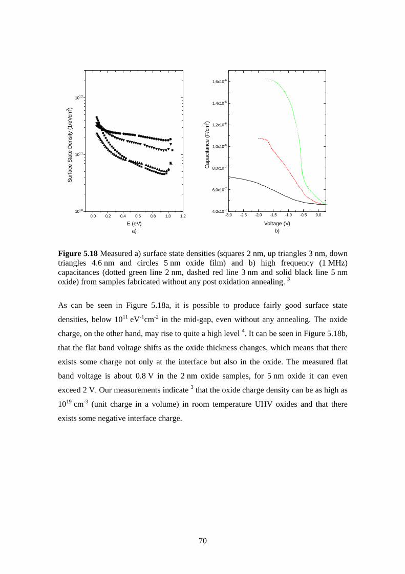
70
0,0 0,2 0,4 0,6 0,8 1,0 1,21010
1011
1012
Sur
face
Sta
te D
ensi
ty (
1/eV
cm2 )
E (eV)a)
-3,0 -2,5 -2,0 -1,5 -1,0 -0,5 0,04,0x10-7
6,0x10⁻⁷
8,0x10⁻⁷
1,0x10⁻⁶
1,2x10⁻⁶
1,4x10⁻⁶
1,6x10⁻⁶
Cap
acita
nce
(F/c
m2 )
Voltage (V)b)
Figure 5.18 Measured a) surface state densities (squares 2 nm, up triangles 3 nm, downtriangles 4.6 nm and circles 5 nm oxide film) and b) high frequency (1 MHz)capacitances (dotted green line 2 nm, dashed red line 3 nm and solid black line 5 nmoxide) from samples fabricated without any post oxidation annealing. 3
As can be seen in Figure 5.18a, it is possible to produce fairly good surface state
densities, below 1011 eV-1cm-2 in the mid-gap, even without any annealing. The oxide
charge, on the other hand, may rise to quite a high level 4. It can be seen in Figure 5.18b,
that the flat band voltage shifts as the oxide thickness changes, which means that there
exists some charge not only at the interface but also in the oxide. The measured flat
band voltage is about 0.8 V in the 2 nm oxide samples, for 5 nm oxide it can even
exceed 2 V. Our measurements indicate 3 that the oxide charge density can be as high as
1019 cm-3 (unit charge in a volume) in room temperature UHV oxides and that there
exists some negative interface charge.
71
0,0 0,2 0,4 0,6 0,8 1,0 1,21010
1011
1012
Sur
face
Sta
te D
ensi
ty (1
/eVc
m2 )
E (eV)
Figure 5.19 Measured surface state density after annealing at 750 oC (triangles) and300 oC (squares). Film thickness around 4 nm. 3
After annealing the surface state densities are still about the same or slightly better than
before it (Figure 5.19). Even 300 oC seems to be enough to improve surface state
density. The oxide charge, on the other hand, changes more (Figure 5.20b). It can be
almost completely removed by annealing at 750 oC. At the same time the interface
charge shifts in a positive direction. It is more difficult to analyze the effect of post
metallization annealing. The depletion region capacitance seems to behave quite well: in
every sample the capacitance curve starts to rise at the same voltage value (Figure
5.20a). The accumulation capacitance, by contrast, only reaches its saturation value at
rather high voltages. This may be caused by impurities from the metal or from the
furnace, which act as a moving charge. Adjustment of the annealing time could help the
results. An encouraging observation was that neither of these annealings decrease the
layer thickness. 3
72
-4 -3 -2 -1 0 1
4,0x10⁻⁷
6,0x10⁻⁷
8,0x10⁻⁷
1,0x10⁻⁶
1,2x10⁻⁶
Cap
acita
nce
(F/c
m2 )
Voltage (V)a)
-3 -2 -1 0
4,0x10⁻⁷
6,0x10⁻⁷
8,0x10⁻⁷
1,0x10⁻⁶
1,2x10⁻⁶
Cap
acita
nce
(F/c
m2 )
Voltage (V)b)
Figure 5.20 Measured high frequency capacitances after annealing at a) 300 oC and b)750 oC 3 (oxide film thicknesses from 2.6 to 5.8 nm).
5.7 Evaporation Technique
A major drawback of the room temperature process is that it is quite slow. The
maximum thickness that can be reached is no more than about one nanometer 12.
Therefore if thicker layers are required, the oxidation process will have to be repeated a
sufficient number of times, with a thin, no more than 0.6 nm, silicon layer evaporated
on top of the sample between each oxidation cycle 2. We have experimented with a
method in which oxidation and silicon evaporation are performed simultaneously. This
significantly reduces the processing time. A quite similar approach has recently also
been used elsewhere. In the so-called low-temperature low-pressure PEE (Plasma-
enhanced Evaporation) process, argon is fed into a plasma source as the working gas for
the discharge, while oxygen is let directly into the chamber 162,163. The cracked oxygen
molecules then oxidize the silicon that is simultaneously evaporated. The surface state
densities reached are at the level of 1011 - 1012 eV-1cm-2 and the oxide charge 1011 -
1012 cm-2. The material density, however, is presumed to be low 162. The relative
73
dielectric constant (εox) can reach values as high as 8 - 10, which can be assumed to be
due to the oxide structural change and, as the net charge is low, local polarization.
5.7.1 Experiment
The substrates used in this study were p-type, 10 Ωcm, (100) silicon wafers. Samples
were cleaned using a chemical cleaning process (5 minute ultrasonic in acetone and
isopropyl alcohol, 10 minutes at 80 oC in H2O:NH4OH:H2O2 (5:1:1) and
H2O:HCl:H2O2 (5:1:1)). The processing tool used was the same modified VG Semicon
V80M molecular beam epitaxy (MBE) system as employed earlier 153. In this process
silicon is electron beam evaporated from a cell after the oxygen plasma has been turned
on. The oxygen is fed through an inlet, controlled by a mass flow controller. The gas is
activated in a plasma cell by using a 265 W RF-field.
Once the samples had been inserted into the UHV growth chamber the native oxide was
removed in situ by raising the temperature to 780 oC and allowing a low silicon flux
etch the oxide off. Oxide removal was verified by monitoring the surface by RHEED.
Great care has to be exercised when working with plasma. Although it increases the
process rate, it can also on the other hand damage the surface. One way to avoid this is
to use some remote plasma-enhanced process (e.g. 162) in which a working gas is fed
into the plasma source and process gas directly into the chamber. In our case we fed the
oxygen directly through the plasma cell, while a silicon flux was generated by e-beam
evaporation into the chamber. This simplifies the process and the equipment set-up. To
avoid creating damage, we opted to use a slow room temperature process in a UHV
chamber which decreases the energies of the oxygen molecules colliding with the
surface. Also, we first grew a one nanometer thick silicon dioxide layer by oxidizing the
silicon wafer surface by oxygen plasma at room temperature as described in chapter 5.4.
This was done not just to form a protective layer but to improve the quality of the
silicon/silicon dioxide interface. Another benefit is that an oxide layer even as thin as
1 nm acts as a diffusion barrier at room temperature 164. This allows for more accurate
adjustment of layer thickness. This first layer was formed by feeding pure oxygen gas
74
for ten minutes through a plasma cell in which RF power was 265 W. The pressure in
the chamber during oxidation was about 5.10-5 mbar, the oxygen flow was 1.2 sccm.
As soon as the first oxide layer is complete, silicon evaporation is started. The oxide
thickness is defined by adjusting the silicon flux and evaporation time. The silicon
evaporation rate was defined by using a Sycon Instruments STC-200 Deposition Rate
Controller. The silicon flux was 0.07 nm/s. Some previous samples have been
characterized by Auger measurement, which has indicated that the use of these
parameters produces silicon dioxide.
The samples were annealed in UHV conditions at 750 oC for 15 minutes. Some
reference samples were fabricated without any annealing. On top of the silicon dioxide
layer 100 nm of aluminum was evaporated. The test structures were then patterned by
using photolithography and wet chemical etching (Figure 5.21). The area of the devices
from which the presented results have been measured is about (100 µm)2.
Figure 5.21 Schematic illustration of the MOS structure.
Our experiments have shown that the process described produces silicon dioxide layers
with surface state densities of around 1.1011 eV-1cm-2 in the mid-gap even without any
annealing (Figure 5.22). This result is the same as that achieved with the ultra high
vacuum plasma oxidation process 2, which was used for the oxidation of the first
nanometer thick layer. However, the oxide charge tends to be quite high, which can be
seen from the flat band voltage shift in the high frequency capacitance measurements
(Figure 5.23). Values of around 1013 cm-2 have been measured.
75
0,0 0,2 0,4 0,6 0,8 1,01010
1011
1012
1013
Sur
face
Sta
te S
ensi
ty (e
V-1cm
-2)
Energy (eV)
Figure 5.22 Surface state densities from MOS sample fabricated at room temperaturewithout annealing.
-2,5 -2,0 -1,5 -1,0 -0,5 0,0
0,0
2,0x10⁻⁷
4,0x10⁻⁷
6,0x10⁻⁷
8,0x10⁻⁷
Cap
acita
nce
(F/c
m2 )
Voltage (V)
Figure 5.23 High frequency capacitance from thin oxide MOS samples fabricated atroom temperature without annealing. Oxide thickness is 4.75 nm (solid black line) and6 nm (dashed red line).
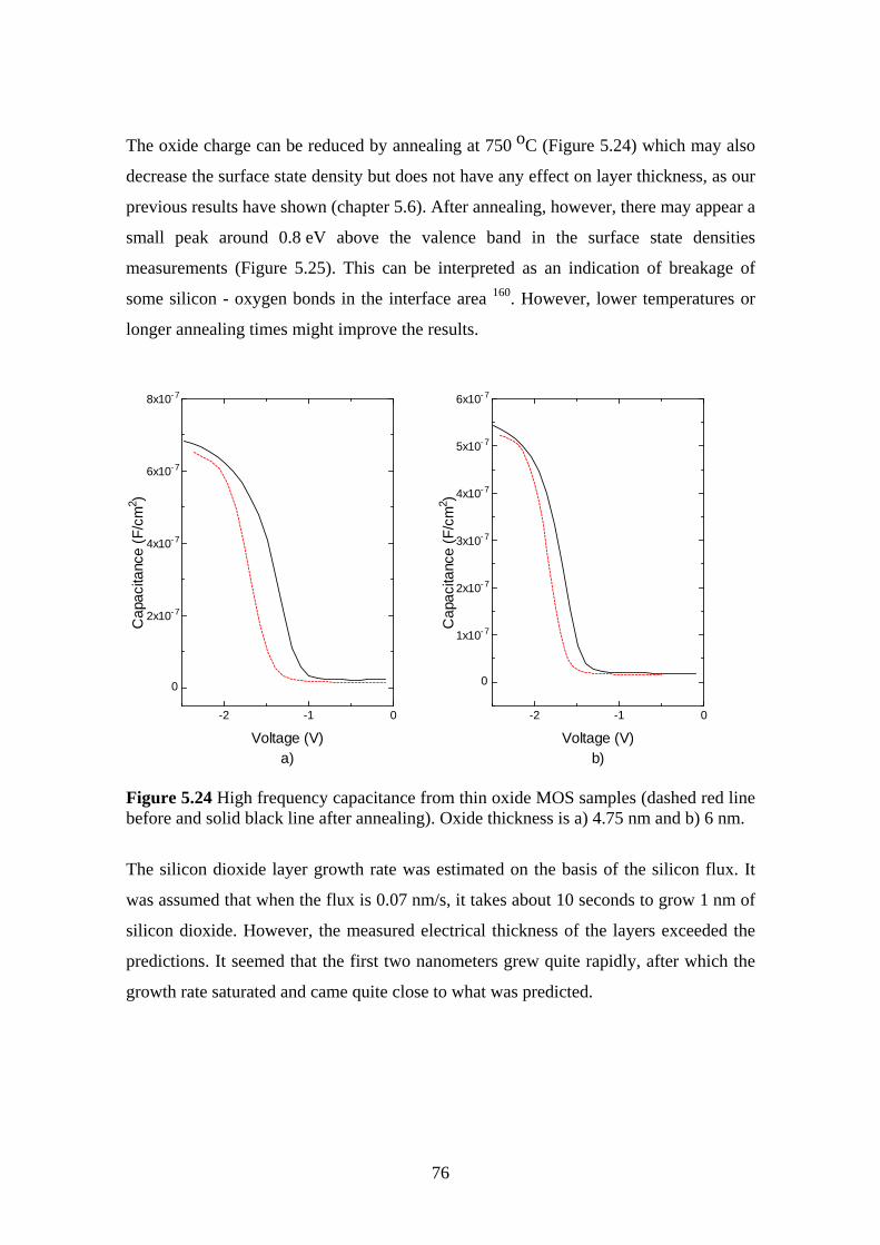
76
The oxide charge can be reduced by annealing at 750 oC (Figure 5.24) which may also
decrease the surface state density but does not have any effect on layer thickness, as our
previous results have shown (chapter 5.6). After annealing, however, there may appear a
small peak around 0.8 eV above the valence band in the surface state densities
measurements (Figure 5.25). This can be interpreted as an indication of breakage of
some silicon - oxygen bonds in the interface area 160. However, lower temperatures or
longer annealing times might improve the results.
-2 -1 0
0
2x10⁻⁷
4x10⁻⁷
6x10⁻⁷
8x10⁻⁷
Cap
acita
nce
(F/c
m2 )
Voltage (V)a)
-2 -1 0
0
1x10⁻⁷
2x10⁻⁷
3x10⁻⁷
4x10⁻⁷
5x10⁻⁷
6x10⁻⁷
Cap
acita
nce
(F/c
m2 )
Voltage (V)b)
Figure 5.24 High frequency capacitance from thin oxide MOS samples (dashed red linebefore and solid black line after annealing). Oxide thickness is a) 4.75 nm and b) 6 nm.
The silicon dioxide layer growth rate was estimated on the basis of the silicon flux. It
was assumed that when the flux is 0.07 nm/s, it takes about 10 seconds to grow 1 nm of
silicon dioxide. However, the measured electrical thickness of the layers exceeded the
predictions. It seemed that the first two nanometers grew quite rapidly, after which the
growth rate saturated and came quite close to what was predicted.
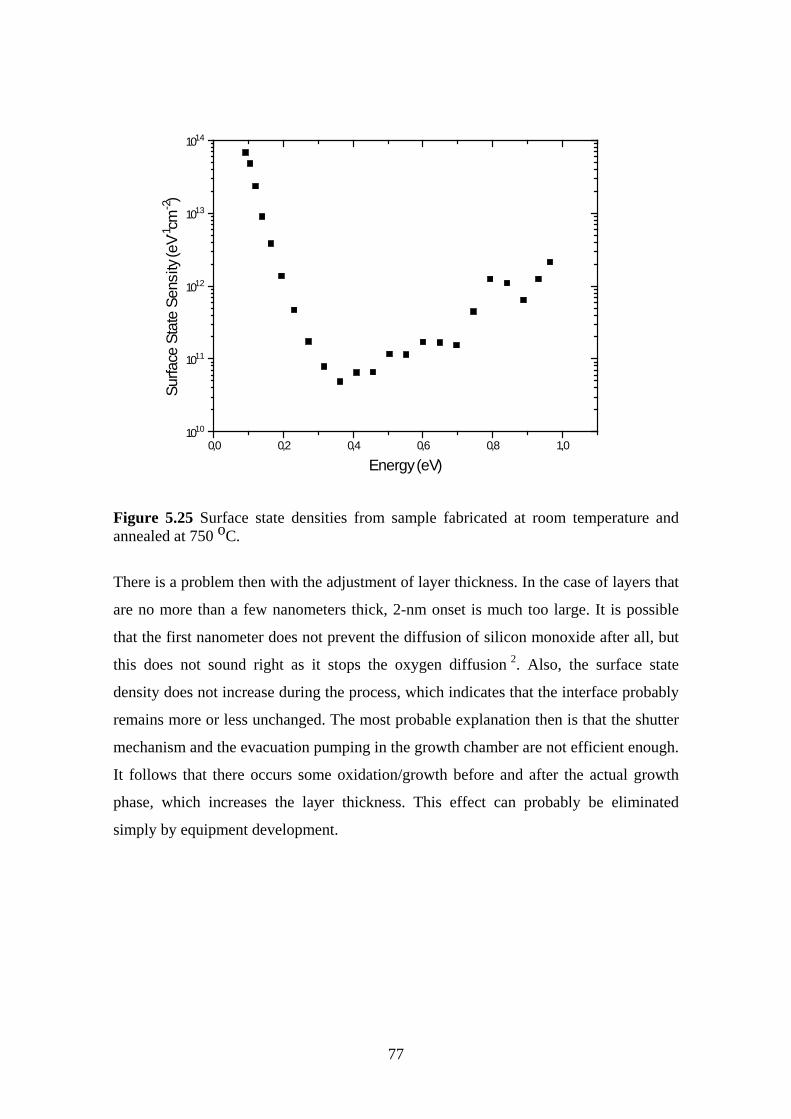
77
0,0 0,2 0,4 0,6 0,8 1,01010
1011
1012
1013
1014
Sur
face
Sta
te S
ensi
ty (e
V-1cm
-2)
Energy (eV)
Figure 5.25 Surface state densities from sample fabricated at room temperature andannealed at 750 oC.
There is a problem then with the adjustment of layer thickness. In the case of layers that
are no more than a few nanometers thick, 2-nm onset is much too large. It is possible
that the first nanometer does not prevent the diffusion of silicon monoxide after all, but
this does not sound right as it stops the oxygen diffusion 2. Also, the surface state
density does not increase during the process, which indicates that the interface probably
remains more or less unchanged. The most probable explanation then is that the shutter
mechanism and the evacuation pumping in the growth chamber are not efficient enough.
It follows that there occurs some oxidation/growth before and after the actual growth
phase, which increases the layer thickness. This effect can probably be eliminated
simply by equipment development.
78
6 Conclusions
We have fabricated 1 - 10 nm thick silicon dioxide layers by plasma oxidation of silicon
in ultra high vacuum (UHV). The UHV chamber is a very clean environment where
both temperature and molecule fluxes are easy to control. The main benefit of the room
temperature MBD (Molecular Beam Deposition) method is that it allows us to fabricate
versatile nanosize silicon-based heterostructures in situ.
In the temperature range 700 - 850 oC, oxidation is initially very slow. Once an uniform
layer has developed on the surface, the growth rate increases. At this stage the
increasing temperature also acts to accelerate the growth rate. During initial growth the
temperature dependence is probably the exact opposite. In thermal oxidation the oxide
quality improves with increasing oxidation temperature. Our MBE system, however,
limits the oxidation temperatures to below 850 oC. Because of the oxidation rate, on the
other hand, we have to use temperatures over 650 oC to achieve thicknesses over 2 nm,
otherwise the oxidation procedure has to be performed gradually one nanometer at a
time. Our measurements predict that in order to get a good quality as-grown layer with
this process, the oxidation temperature should be at least 700 oC.
Since high temperatures are not always desirable in processing, we have also studied
room temperature oxidation. The room temperature ultrahigh vacuum plasma oxidation
method has been proven to produce good quality ultrathin silicon dioxide layers, with
quite accurately controllable layer thickness, relatively high breakdown fields and low
surface state densities. It is predicted, that as higher temperatures smoothen the surface,
lower temperatures do not create as much roughness in the first place. At the room
temperature the oxidation saturates at around 1 nm which means that the fabrication
process can be so designed that it is fully automated, even if the system incorporates no
thickness measurement of amorphous layers. Also, processing does not require high
temperatures. The only exception is native oxide removal, where we use a temperature
of 780 oC. However, even this can be avoided by using chemical etching and
passivation of the sample surface. The precise effects of this on layer quality remain to
be seen, though.
79
The ultrahigh vacuum plasma oxidation method seems to produce quite homogenous
silicon/silicon dioxide interface state densities, regardless of the oxidation temperature.
In layers oxidized at room temperature, however, the oxide charge tends to rise to quite
a high level. Some kind of annealing should therefore be used to decrease the oxide
charge. Our measurements showed that post oxidation UHV annealing at 750 oC and
post metallization annealing at 350 oC in air slightly decrease the surface state densities.
The oxide charge, which is quite high in these oxides, can be decreased by UHV
annealing. The effect of post metallization annealing on the oxide charge is less clear.
This is probably due to impurity diffusion. Neither of the annealings used decrease the
oxide layer thickness. This backs up our experiments which show that the desorption of
silicon dioxide from the silicon surface starts quite abruptly at 870 oC under a
background pressure of 10-10 mbar 1. This means that temperatures at least up to 750 oC
can safely be used when there is no protective layer covering the silicon dioxide film.
The silicon dioxide layers fabricated by evaporating silicon in a low pressure oxygen
plasma ambient seem to have the same surface state densities as layers fabricated by the
room temperature ultrahigh vacuum plasma oxidation method. The main benefit
achieved with this process is the increased growth rate. It also allows the oxide
thickness to be varied over a wider range. The main drawback is the high oxide charge,
but that can be lowered by annealing.
In our studies we have tested the UPO method to produce high quality silicon dioxide
films. The benefits of this method are good thickness control, a pure growth
environment, highly accurate material fluxes, and the possibility of in situ device
processing. However, the as-grown layers, especially those oxidized at room
temperature have a very high oxide charge, even though the interface state density is
reasonably low. The charge can affect on the leakage and the film stability in stressed
conditions can weaken. Our preliminary experiments have shown that the layer quality
can be improved by annealing, but the process needs to be further developed. Because
various oxide fabrication procedures worldwide have been able to produce very high
quality films, the usefulness of our UPO method remains controversial in conventional
IC fabrication. Various thermal oxidation methods (most notably rapid thermal
oxidation) have proven to be accurate and reliable and to produce an extremely high
oxide quality. Nonetheless there do remain other purposes for our process. Accurately
80
controlled system can supply much information about the oxidation process itself. It
also can be used in device fabrication and then the most logical choice seems to be the
fabrication of the silicon/silicon dioxide heterostructures. For this purpose the process
has to be carefully adjusted and studied because the interface quality has to be even
better than in MOSFETs so that really separate quantum states may be formed. The
possibility of making fully crystalline structures seems to be particularly interesting.
The most probable crystalline form of SiO2 in low pressures in the temperature range
870 - 1470 oC is tridymite 165. However, processing will require a deep understanding of
the oxidation mechanisms and the parameters affecting these mechanisms. In addition,
the substrates used have to be of a very high quality and low resistivity, with epitaxial
buffer layers to form an atomically flat surface. It is likely that even quite small changes
in oxidation temperatures or oxidation rates will produce different oxide species.
Surface roughness causes local tensions during oxidation and in this way prevents
homogenous film formation. Traditionally hydrogen has been used to passivate
dangling bonds, but this is probably not the best method to use when fabricating
quantum devices because it can affect the interface charge as well as interface state
generation. Nitrogen incorporation into the oxide also has many beneficial properties,
but it can have an adverse effect on interface quality.
81
References
1 T. Majamaa, V.-M. Airaksinen, J. Sinkkonen, Appl. Surf. Sci. 107 (1996), 1722 T. Majamaa, O. Kilpelä, S. Novikov, Appl. Surf. Sci., 136 (1998), 173 T. Majamaa, O. Kilpelä, S. Novikov, J. Sinkkonen, Appl. Surf. Sci. 142 (1999), 3514 T. Majamaa, O. Kilpelä, Physica Scripta T79 (1999), 2595 W. Kiunke, E. Hammerl, I. Eisele, J. Crystal Growth 127 (1993) 736 H. Gossner, I. Eisele, L. Risch, Jpn. J. Appl. Phys. 33, Part I (1994) 24237 K. Watanabe, S. Kimura, T. Tatsumi, Jpn. J. Appl. Phys. 38 (1999) L10558 A. Strass, P. Bieringer, W. Hansch, V. Fuenzalinda, A. Alvarez, J. Luna, I. Martil,
F.L. Martinez, I. Eisele, Thin Solid Films 349 (1999) 1359 Y. Taur, P.A. Buchanan, W. Chen, D.J. Frank, K.E. Ismai, S.-H. Lo, G.A. Sai-
Halasz, R.G. Viswanathan, H.-J. C. Wann, S.J. Wind, H.-S. Wong, Proc. IEEE 85
(1997), 48610 S. Tiwari, F. Rana H. Hanfi, A. Hartstein, E. F. Crabbé, K. Chan, Appl. Phys.
Lett. 68 (1996), 137711 P. Masson, G. Ghibaudo, J.L. Autran, P. Morfouli, J. Broni, Electr. Lett. 34
(1998), 197712 S. Novikov, J. Sinkkonen, O. Kilpelä, S.V. Gastev, J. Vac. Sci Technol. B, 15
(1997) 147113 A.C. Seabaugh, C.-C. Cho, R.M. Steinhoff, T.S. Moise, S. Tang, R.M. Wallace,
E.A. Beam, Y.-C. Kao, R.C. Bowen, W.R. Frensley, K. H. Park, Y. Okuno, 2nd
International Workshop on Quantum Functional Devices, Matsue, Japan, May 23-
25 199514 M. Hacke, H.L. Bay, S. Mantl, Thin Solid Films, 280 (1996), 10715 J.H. Stathis, D.J. DiMaria, Microelectronic Engineering, 48 (1999), 39516 H.S. Momose, M. Ono, T. Yoshitomi, T. Ohguro, S. Nakamura, M. Saito, H.
Iwai; IEEE Transactions on Electron Devices, 43 (1996), 123317 A. Chin, W.J. Chen, T. Chang, R,H, Kao, B.C. Lin, C. Tsai, J.C.-M. Huang, IEEE
Electr. Dev. Lett. 18 (1997) 41718 B.E. Deal, IEEE Trans. El. Dev. ED-27 (1980), 60619 D.M. Fleetwood, IEEE Trans. Nucl. Sci. NS-39 (1992) 26920 M. J. Uren, S. Collins, M.J. Kinton, Appl. Phys. Lett. 54 (1989), 1448
82
21 D.A. Buchanan, D.J. DiMaria, J. Appl. Phys. 67 (1990) 743922 M.E. Zvanut, F.J. Feigl, W.B. Fowlerm, J. K. Rudra, P.J. Caplan, E.H. Poindexter,
J.D. Zook, Appl. Phys. Lett. 54 (1989), 211823 T. Ohmi, M. Morita, T. Hattori: The Physics and Chemistry of SiO2 and the Si-
SiO2 Interface; Plenum (1988), 41324 H. Nohira, T. Hattori, Appl. Surf. Sci. 117/118 (1997), 11925 H. Nohira, A. Omura, M. Katayama, T. Hattori, Appl. Surf. Sci. 123/124 (1998),
54626 H. Kageshima, K. Shiraishi, Phys. Rev. Lett. 81 (1998), 593627 A. Pasquarello, M.S. Hybertsen, R. Car, Nature 396 (1998), 5828 X. Chen, J.M. Gibson, Appl. Phys. Lett. 70 (1997), 146229 Devine, Appl. Phys. Lett., 68 (1996), 310830 T. Hattori, H. Nohira, K. Takahashi, Microelectronic Engineering, 48 (1999), 1731 N. Gonon, J. Ciavatti, C. Plossu, B. Balland, D. Barbier, A. Gagnaire,
Microelectronics Journal 24 (1993) 40132 J. S. Johanssen, W. E. Spicer, J. Appl. Phys. 47 (1976), 302833 C. A. Fenstermaker, F. L. McCracking, Surf. Sci. 16 (1965), 8534 K. Hirose, H. Nohira, T. Koike, K. Sakamo, T. Hattori, Phys. Rev. B 59 (1999)
561735 D-A. Luh, T. Miller, T.C. Chiang, Phys. Rev. Lett. 79 (1997), 301436 R. Haight, L.C. Feldman, J. Appl. Phys. 53 (1983), 488437 A. Pasquarello, Microelectronic Engineering, 48 (1999), 8938 F. J. Grunthaner, P.J. Grunthaner, R.P. Vasques, B.F. Lewis, J. Maserjian, Phys.
Rev. Lett. 43 (1979), 168339 G. Hollinger, E. Bergigna, H. Chermette, F. Himpsel, D. Lohez, M. Lannoo, M.
Bensoussan, Philos. Mag. B 55 (1987), 73540 Y. Iida, T. Shimura, J. Harada, S. Samata, Y. Matsuhita, Surf. Sci. 258 (1991),
23541 I. Takashi, T. Shimura, J. Harada, J. Phys.: Condens. Matter 5 (1993), 652542 C. Kaneta, T. Yamasaki, T. Uchiyama, T. Uda, K. Terakura, Microelectronic
Engineering, 48 (1999), 11743 A. Ourmazd, D.W. Taylor, J. A. Rentschler, J. Bevk, Phys. Rev. Lett. 59 (1087),
213
83
44 A. Pasquarello, M.S. Hybertsen, R. Car, Phys. Rev. Lett. 74 (1995), 102445 A. Pasquarello, M.S. Hybertsen, R. Car, Appl. Phys. Lett. 68 (1996), 62546 S. M. Sze: Semiconductor Devices: Physics and Technology (Wiley, New York,
1985)47 M. Lenzlinger, E.H. Snow, J. Appl. Phys. 40 (1969) 27848 M. Hiroshima, T, Yasaka, S. Miyazaki, M. Hirose, Jpn. J. Appl. Phys. 33 (1994),
39549 S. Zafar, Q. Liu, E.A. Irene, J. Vac. Sci. Technol. A 13 (1995), 4750 A. Scarpa, A. Paccagnella, G. Ghidini, A. Vianello, E. Zanoni, Solid-State
Electronics 41 (1997), 93551 A. Ghetti, E. Sangiorgi, T. Sorsch, I. Kizilyalli, Microelectronic Engineering, 48
(1999), 3152 J. Ahn, A. Joshi, G,Q, Lo, D.-L. Kwong, IEEE El. Dev. Lett. 13 (1992), 51353 M. Depas, T. Nigam, M.M. Heyus; IEEE Transactions on Electron Devices, 43
(1996) 149954 E. Harari, J. Appl. Phys. 49 (1978), 247855 S. Holland, I.C. Chen, T.P. Ma, C. Hu, IEEE El. Dev. Lett. 5 (1984) 30256 J.J. Tzou, C.C. Yao, R. Cheung, H. Chan, IEEE El. Dev. Lett. 7 (1986), 44657 M.-S. Liang, S. Haddad, W. Cox, S. Cagnina, IEDM Tech. Dig. (1986) 39458 S. Ikeda, M. Okihara, H. Ucida, N. Hirashita, Jpn. J. Appl. Phys. 36 (1997), 256159 D.J. Dumin, J.R. Maddux, IEEE Trans. El. Dev. 40 (1993), 98660 J. Maserjan, N. Zamani, J. Vac. Sci. Techn. 20 (1982), 74361 P. Olivo, T.N. Nguyen, B. Riccó, IEEE Trans. El. Dev. 35 (1988), 225962 G.W. Rubloff, K. Hofmann, M. Liehr, D.R. Young, Phys. Rev. Lett. 58 (1987),
237963 D.J. DiMaria, E. Cartier, J. Appl. Phys. 78 (1995), 388364 D.M. Fleetwood, P.S. Winokur, L.C. Riewe, R.A. Reber Jr, J. Appl. Phys. 84
(1998), 614165 M. Kerber, U. Schawalke, G. Innertsberger, Microelectronic Engineering, 48
(1999), 14766 G. Tao, R. Cöp, J. Dijsktra, F. Kuper, R. Verhaar, Microelectronic Engineering,
48 (1999), 41967 Y. Homma, M. Suzuki, N. Yabumoto, J. Vac. Sci & Technol. A10 (1992), 2055

84
68 M. Itsumi, F. Kiyosumi, Appl. Phys. Lett. 40 (1982), 49669 P. Mertens, T. Bearda, M. Houssa, L.M. Loewenstein, I. Cornelissen, S.
De Gendt, K. Kenis, I. Teerlinck, R. Vos, M. Meuris, M.M. Heyns,
Microelectronic Engineering, 48 (1999), 19970 Y. Kobayashi, Y. Shinoda, K. Sugii, Jpn. J. Appl. Phys. 29 (1990), 100471 W. Hansh, E. Hammerl, W. Kiunke, I. Eisele, J. Raum, E. Beck, Jpn. J. Appl.
Phys. 33, Part I (1994) 226372 K.E. Johnson, P.K. Wu, M. Sander, T. Ergel, Surf. Sci. 290 (1993), 21373 G.D. Wilk, Y. Wei, H. Edwards, R.M. Wallace, Appl. Phys. Lett., 70 (1997),
228874 Y. Homma, H. Hibino, T. Ogino, N. Aizawa, Physical Review B, 55 (1997),
R1023775 M. Niwa, T. Kouzaki, K. Okada, M. Udagava, R. Sinclair, Jpn. J. Appl. Phys. 33
(1994), 38876 R.A.B. Devine, W.L. Warren, J.B. Xu, I.H. Wilson, P. Paillet, J.-L. Leray, J.
Appl. Phys. 77 (1995), 17577 J.L. Hansem, S.Y. Shiryaev, E.V. Thomsen, Journal of Crystal Growth, 157
(1994) 31778 T. Ohmi, K. Matsumoto, K. Nakamura, K. Makihara, J. Takano, K. Yamamoto,
Appl. Phys. Lett. 62 (1993), 40579 M. Tabakomori, H. Ikoma, Jpn. J. Appl. Phys. 36 (1997), 540980 H. Fukuda, M. Yasuda, T. Iwabuchi, S. Kameko, T. Ueno, I. Ohdomari, J. Appl.
Phys. 72 (1992), 190681 L. Do Tanh, P. Balk, J. Electrochem. Soc. 135 (1988), 179782 A.H. Carim, R. Sinclair, J. Electrochem. Soc. 134 (1987), 74183 E.P. EerNisse, Appl. Phys. Lett. 35 (1979), 884 M. Itsumi, O. Nakajima, N. Shiono, J. Appl. Phys. 72 (1992), 218585 M. Depas, R.L. Van Meirhaeghe, F. Cardon, Solid-State Electronics 37 (1994)
43386 G. Eftekhari, J. Electrochem. Soc. 140 (1993) 78787 T. Ohmi, M. Morita, A. Teramoto, K. Makihara, K. S. Tseng, Appl. Phys. Lett.,
60 (1992), 212688 A.C. Adams, T.E. Smith, C.C. Chang, J. Electrochem. Soc. 127 (1980) 1787
85
89 R.R Razouk, B.E. Deal, J. Electrochem. Soc. 126 (1979) 157390 K.H. Lee, W.H. Liu, S.A. Campbell, I. Banerjee, J. Electrochem. Soc. 140 (1993)
50191 M. Akizuki, J. Matsuo, S. Ogasawara, M. Harada, A. Doi, I. Yamada, Jpn. J.
Appl. Phys. 35 (1996), 145092 V. Ramgopal Rao, W. Hansch, S. Mahapatra, D.K. Sharma, J. Vasi, T. Grabolla,
I. Eisele, Microelectronic Engineering, 48 (1999), 22393 T. Fuyki, S. Muranaka, H. Matsunami, Appl. Surf. Sci. 117/118 (1997), 12394 P.C. Chen, K.Y.J. Hsu, H.L. Hwang, J.Y. Lin, J. Appl. Phys. 76 (1994), 550895 S. Kimura, E.Murakami, T. Warabisako, H. Sunami, T. Tokuyama, IEEE Electr.
Dev. Lett. 7 (1986) 3896 R. Bartels, A.G. Aberle, R. Hezel, 14th European PVSEC 1997, Barcelona97 S.S. Todorov, E.T. Fossum, J. Vac. Sci. Technol. B, 6 (1988) 46698 K.T. Sung, W.Q. Li, S.H. Li, S.W. Pang, P.K. Bhattacharya, Electronic Letters, 29
(1993) 27799 H. Fukuda, S. Murai, T. Endoh, S. Nomura, J. Appl. Phys. 81 (1997) 1825100 H. Hwang, M.-Y. Hao, J. Lee, V. Mathews, P.C. Fazan, C. Dennison, Solid-State
Eelctronics, 36 (1993), 749101 W.L. Hill, E.M. Voge., V. Misra, P.K. McLarty, J.J. Wortman, IEEE Trans. El.
Dev. 43 (1996), 15102 H. Yang, H. Niimi, Y. Wu, G. Lucovsky, J. Reister, J. Rowe, Microelectronic
Engineering, 48 (1999), 307103 Y.-L. Wu, J.-G. Hwu, IEEE El. Dev. Lett. 14 (1993), 1104 J.S. Cable, R.A. Mann, J.C.S. Woo, IEEE El. Dev. Lett. 12 (1991), 128105 J.S. Cable, J.S.C. Woo, IEEE Trans. El. Dev. Lett. 39 (1992) 607106 B. Yuwono, T. Schloesser, A. Gschwandtner, G. Innersberger, A. Grassl, A.
Olbrich, W.H. Krautschneider, Microelectronic Engineering, 48 (1999), 51107 B. E. Deal, A. S. Grove, J. Appl. Phys. 36 (1965), 3770108 S. Dimitrijev, H.B. Harrison, J. Appl. Phys., 80 (1996), 2467109 A.A. Demkov, O. F. Sankey, Phys. Rev. Lett. 83 (1999) 2038110 S.S. Ang, S.R. Wilson, J. Electronchem. Soc. 134 (1987) 1254111 R. Lathlaen, D.A. Diehl. J. Electrochem. Soc, 116 (1969), 620112 Z. Chen, K. Yasutake, A. Doolittle, A. Rohatgi, Appl. Phys. Lett. 63 (1993), 2117
86
113 W-S. Liao, S-C. Lee, J. Appl. Phys. 80 (1996), 1171114 S.S. Ang, Y.J. Shi, W.D. Brown, J. Appl. Phys. 73 (1993) 2397115 G.G. Fountain, R.A. Rudder, S.V. Haltangadv, R.J. Markunas, J. Appl. Phys. 63
(1988) 4744116 A.P. Gurevich, M.K. Weldon, Y.J. Chabal, R.L. Opila, J. Sapjeta, Appl. Phys.
Lett. 74 (1999), 1257117 V. Ramgopal Rao, W. Hansch, H. Baumgärtner, I. Eisele, P.K. Sharma, J. Vasi, T.
Grabolla, Thin Solid Films 296 (1997), 37118 T. Yasudda, Y. Ma, S. Habermehl, G. Lucovsky, Appl. Phys. Lett. 60 (1992), 434119 P. Masson, P. Morfouli, J. Autran, J. Wortmann, Microelectronic Engineering, 48
(1999), 211120 U. Neuwald, A. Feltz, U. Memmert, R.J. Behm, J. Appl. Phys. 78 (1995), 4131121 J.A. Bardwell, K.B. Clark, D.F. Mitchell, D.A. Bisaillion, G.I. Sproule, B.
MacDougall, M.J. Graham, J. Electrochem. Soc. 141 (1993), 2135122 J.A. Bardwell, N. Draper, P. Schmuki, J. Appl. Phys. 79 (1996), 8761123 J.A. Bardwell, P. Schmuki, G.I. Sproule, D. Landheer, D.F. Mitchell, J.
Electrochem. Soc. 142 (1995), 3933124 O. Sneh, M.L. Wisem A.W. Ott, L.A. Okada, S.M. George, Surf. Sci. 334 (1995)
135125 J.W. Klaus, A.W. Ott, J.M. Johnson, S.M. George, Appl. Phys. Lett. 70 (1997)
1092126 O. Sneh, S.M. George, J. Phys. Chem. 99 (1994) 4639127 S. Morishita, Y. Uchida, M. Matsumura, Jpn. J. Appl. Phys. 34 (1995) 5738128 K. Hara, Y. Suzuki, Y. Taga, Jpn. J. Appl. Phys. 18 (1979), L2027129 W.K. Choi, C.K. Choo, Y.F. Lu, J. Appl. Phys. 80 (1996) 5837130 Y. Wei, R.M. Wallace, A.C. Seabaugh, Appl. Phys. Lett. 69 (1996), 1270131 J. Lander, J. Morrison, J. Appl. Phys. 33 (1962), 2098132 R. Tromp, G. W. Rubloff, P. Balk, F.K. LeGoues, J. Van Loenen, Phys. Rev. Lett.
55 (1985), 2332133 M. Liehr, J. E. Lewis, G.W. Rubloff, J. Vac. Sci. Technol. A5 (1987) 1559134 Y. Wei, R.M. Wallace, A.C. Seabaugh, Appl. Phys. Lett. 69 (1996) 1270135 W.L. Warren, D.M. Fleetwood, M.R. Shaneyfelt, J.R. Schwank, P.S. Winokur,
R.A.B. Devine, D. Mathiot, Appl. Phys. Lett. 64 (1994), 3452
87
136 R.A.B. Devine, D. Mathiot, W.L. Warren, D.M. Fleetwood, B. Aspar, Appl. Phys.
Lett. 63 (1993), 2926137 A. Stesmans, V.V. Afanas’ev, Microelectronic Engineering, 48 (1999), 113138 A. Stesmans, V.V. Afanas’ev, Phys. Rev. B 54 (1996), R11129139 W.L. Warren, K. Vandheusden, J.R. Scwank, D.M. Fleetwood, P.S. Winokur,
R.A.B. Devine, Appl. Phys. Lett. 68 (1996), 2993140 A. Hartstein, D.R. Youn, Appl. Phys. Lett. 38 (1981), 631141 A. Stesmans, V.V. Afanas’ev, Microelectronic Engineering, 48 (1999), 131142 R.S. Bauer, R.Z. Bachrach, L.J. Brillson, Appl. Phys. Lett. 37 (1980), 1006143 M.H. Hecht, R.P. Vasques, F.J. Grunthaner, N. Zamari, J. Maserjian, J. Appl.
Phys. 57 (1985), 5256144 P. Balk, The Electrochem. Soc. Meeting, Buffalo, NY, Oct. 10-14, 1965145 K. Hofmann, G. W. Rubloff, D.R. Young, J. Appl. Phys. 61 (1987), 4584146 T. Majamaa: Computing the Charge in the Inversion Layer of MOSFET; (in
Finnish) Special Project in Materials Physics, Department of Technical Physics,
Helsinki University of Technology (1992), p 27+7147 K.S. Krisch, J.D. Buedo, L. Mauchanda, IEEE El. Dev. Lett. 17 (1996), 521148 HP4192A Impedance Analyzer Instructions Manual149 J. Ritola: Impedanssispektroskopia- ja kapasitanssimittausjärjestelmä; Sovelletun
fysiikan erikoistyö, Teknillisen fysiikan osasto/Tkk (1994),pp 18+49150 C.-Y. Hu, D. L. Kencke, S. Banerjee, B. Bandyopadhyay, E. Ibok, S. Garg, Appl.
Phys. Lett. 66 (1995), 1638151 E.H. Nicollian, A. Goetsberger, Bell Syst. Tech. J. 46 (1967), 1055152 E.H. Nicollian, J.R. Brews: MOS (Metal Oxide Semiconductor) Physics and
Technology; John Wiley & Sons (1982) 906153 V.M. Airaksinen, J. Kaitila, H. Niemi, J. Lahtinen, J. Saarilahti, Physica Scripta
T54 (1994), 205154 F.W. Smith, G. Ghidini, J. Electrochem. Soc: Solid State Science and
Technology, 129 (1982), 1300155 Y. Mii, S. Rishton, Y. Taur, D. Kern, T. Lii, K. Lee, K.A. Jenkins, D. Quinlan, T.
Brown Jr, D. Danner, F. Sewell, M. Polcari, IEEE Electr. Dev. lett. 15 (1994), 28156 T. Tuurnala, T. Majamaa, Physica Scripta T69 (1997), 310157 M.P. D'Evelyn, M.M. Nelson, T. Engel, Surf. Sci., 186 (1987), 75
88
158 H. Z. Massoud, Solid-State Eelctronics, 41 (1997), 929159 V.D. Borman, E.P. Gusev, Y.Y. Lebedinski, V.I. Troyan, Phys. Rev. B, 49
(1994), 5415160 S.A. Nelson, H.D. Hallen, R.A. Buhrman, J. Appl. Phys. 63 (1988), 5027161 P. Lundgren: Electrically Active Defects in Metal - Tunnel Oxide - Silicon
(MTOS) Devices (Department of Solid State Electronics, Chalmers University of
Technology, 1994)162 A. Neubecker, P. Bieringer, W. Hansch, I. Eisele, J. Crystal Growth 157 (1995),
201163 A. Strass, W. Hansh, A. Neubecker, P. Bieringer, A. Fischer, I. Eisele, Vacuum
48 (1997) 701164 T. Majamaa, V.-M. Airaksinen, S. Novikov, Physica Scripta, T69 (1997), 215165 C. R. Helms, E. H. Poindexter, Rep. Prog. Phys. 57 (1994) 791