ultrathin rechargeable all-solid-state batteries based on monolayer graphene
TRANSCRIPT

Journal ofMaterials Chemistry A
PAPER
Dow
nloa
ded
by U
nive
rsity
of
Nor
th C
arol
ina
at C
hape
l Hill
on
15/0
4/20
13 1
0:19
:56.
Pu
blis
hed
on 0
9 Ja
nuar
y 20
13 o
n ht
tp://
pubs
.rsc
.org
| do
i:10.
1039
/C3T
A01
183F
View Article OnlineView Journal | View Issue
aNokia Research Center, Broers Building,
Cambridge, UK. E-mail: [email protected] S.A., Tolosa Hiribidea 76, 2001cCIC nanoGUNE, Tolosa Hiribidea 76, 2001dIKERBASQUE, Basque Foundation for Scien
† Electronic supplementary information (Echaracterization of a monolayer graphene
Cite this: J. Mater. Chem. A, 2013, 1,3177
Received 21st November 2012Accepted 9th January 2013
DOI: 10.1039/c3ta01183f
www.rsc.org/MaterialsA
This journal is ª The Royal Society of
Ultrathin rechargeable all-solid-state batteries based onmonolayer graphene†
Di Wei,*a Samiul Haque,a Piers Andrew,a Jani Kivioja,a Tapani Ryhanen,a
Amaia Pesquera,b Alba Centeno,b Beatriz Alonso,b Andrey Chuvilincd
and Amaia Zurutuzab
The energy and power requirements of portable electronic devices and electric vehicles are ever increasing,
driving research into novel battery structures with increased volumetric energy and power densities.
Existing energy storage technologies cannot satisfy both of these requirements. There are many reports
on the application of graphene in batteries and supercapacitors with enhanced power and energy
densities; however, few results were shown on the performance of an electrochemical energy storage
device made of monolayer graphene. The energy storage capability of monolayer graphene is
investigated in this paper and it can contribute an understanding of the application of graphene
materials in high energy and power density batteries. In parallel, flexible solid-state batteries will relax
design constraints, giving the freedom to create new device form factors. A mechanically flexible all-
solid state battery can be made of monolayer graphene grown by chemical vapour deposition (CVD)
directly onto copper (Cu) foil. The total thickness of the resulting battery was �50 mm. Such an ultrathin
battery showed the highest energy density of 10 W h L�1 and the highest power density of 300 W L�1.
It also shows excellent cyclic stability and sustains a discharge current density of 100 mA cm�2 over
100 cycles, maintaining energy capacity over 0.02 mA h cm�2.
1 Introduction
Graphite is the current industry standard material for lithiumbattery electrodes due to its reliability and effective lithium ionintercalation properties. Two-dimensional graphene is the basiccomponent in all different graphitic forms of materials rangingfrom the three-dimensional graphite, one-dimensional carbonnanotubes to zero-dimensional fullerenes. Carbon nanotubesand other carbon nanomaterials had been utilized as novelelectrode materials to enhance battery capacity and exibleform factors.1 However, unmodied carbon nanotubes are notideal candidate materials to be dispersed in either organic oraqueous solutions for wet-processing methods such as printingor spin-coating. Graphene-based materials are intriguing fromthe perspectives of both fundamental science and technology,because they can be easily formulated as ink, are chemicallyand thermally tolerant, electrically conductive and mechan-ically robust. Graphene has superior electrical conductivityto graphitic carbon, a high specic surface area of over
21 J. J. Thomson Avenue, CB3 0FA,
8 Donostia-San Sebastian, Spain
8 Donostia-San Sebastian, Spain
ce, E-48011, Bilbao, Spain
SI) available: TEM and electrochemicalbattery. See DOI: 10.1039/c3ta01183f
Chemistry 2013
2600 m2 g�1,2 and a broad electrochemical window that wouldbe very advantageous for application in energy storage devices.Graphene sheets can be used as electrode materials with highrate capability and large capacity for rechargeable lithiumsecondary batteries due to their large reversible Li storageability.2–6 Studies of lithium storage and the use of graphene as ahigh-performance battery electrode have been carried out.7,8 Itis feasible to make electrochemical energy devices with bothhigh energy and power density that can also work at highfrequencies by using graphene.9,10 Few-layer, nitrogen-dopedgraphene was used as a battery electrode and its rate capabilitywas studied for current densities ranging from 1 mA cm�2 to100 mA cm�1.4 The nominal capacity (�0.06 mA h cm�2) wasobtained for a discharge rate of 1 mA cm�2.
To produce graphene, many methods have already beendeveloped.11–13 In 2004, Geim and co-workers12 rst reportedgraphene sheets prepared by micromechanical exfoliation(repeated peeling) of highly oriented pyrolytic graphite (HOPG).This scotch-tape method produces graphene with excellentmaterial properties and hence is still widely used in manylaboratories to obtain pristine graphene akes for basic scien-tic research and for making proof-of-concept devices. Theprocess is, however, not suitable for volume production and theake size is limited to the micrometer range. Graphene can alsobe prepared by thermal decomposition of a SiC wafer underultrahigh vacuum conditions14 but the resulting graphene is
J. Mater. Chem. A, 2013, 1, 3177–3181 | 3177
Journal of Materials Chemistry A Paper
Dow
nloa
ded
by U
nive
rsity
of
Nor
th C
arol
ina
at C
hape
l Hill
on
15/0
4/20
13 1
0:19
:56.
Pu
blis
hed
on 0
9 Ja
nuar
y 20
13 o
n ht
tp://
pubs
.rsc
.org
| do
i:10.
1039
/C3T
A01
183F
View Article Online
composed of submicrometer-sized domains, which are notspatially uniform in size or number density over larger lengthscales. Chemical Vapour Deposition (CVD) is a popular tech-nique to grow graphene on metal substrates.13 CVD has thepotential to enable large scale graphene production for elec-tronic applications such as thin lm transistors, solar cells andtouch panels which require large area graphene sheets of theorder of tens of centimeters in size. Using this process, gra-phene may be subsequently transferred to a separate substrate.Alternative cost-effective ways of graphene synthesis usingsolution-based processes are via chemical reduction of gra-phene oxide (GO)11 or liquid phase exfoliation starting fromgraphite.15 These methods offer the scope to produce largequantities of graphene economically to the expense of aconsiderable decrease in graphene quality/properties. Inparticular, chemical reduction of GO is a simple process andsheets as large as 50 micrometers have been made, and they canthen be subsequently chemically modied. Within the family ofchemical methods, the recently developed process of electro-chemical exfoliation is regarded as a green method that allowseasy tunability of the obtained products by variation of theapplied potential.16–18 Chemical reduction of graphene oxidehas been a cost-effective method of synthesis of grapheneelectrodes for Li batteries5 but many defects are created duringthe reaction and these defects increase sheet resistance,reducing the open circuit voltage of the battery. It is also harderto control the number of layers deposited than it is with theCVD method. In this paper, graphene monolayer lms weregrown on Cu foil using CVD and their application as a batteryelectrode was studied, demonstrating important advantages forexible batteries.
2 Results and discussion
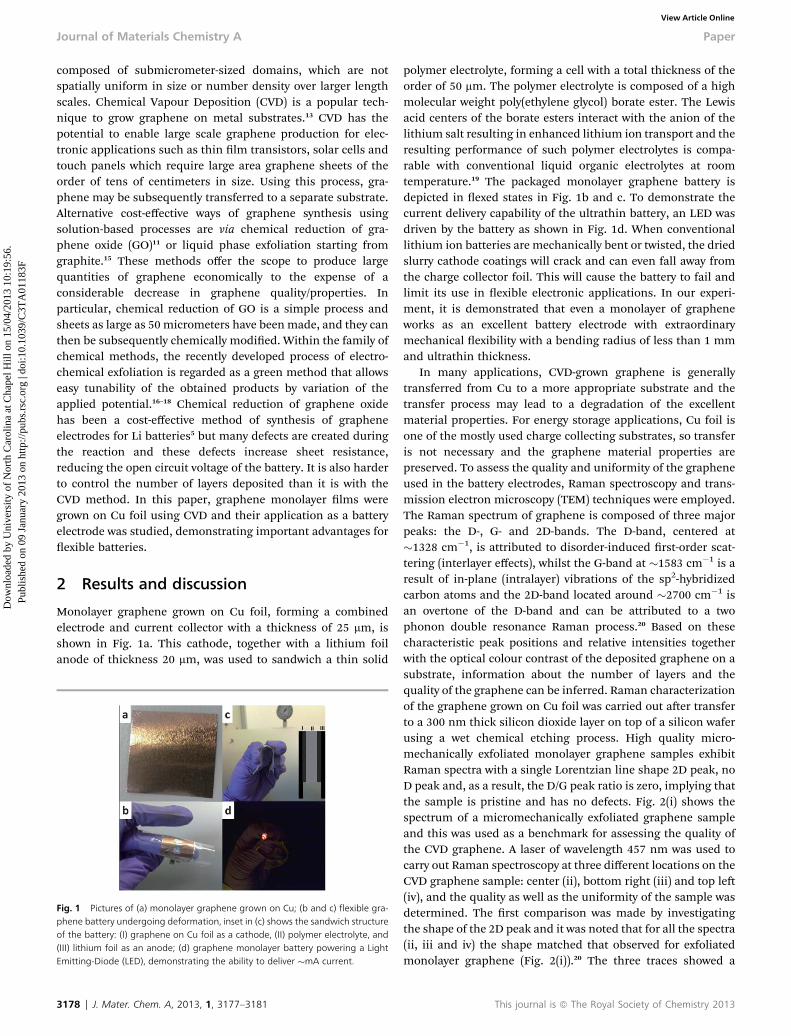
Monolayer graphene grown on Cu foil, forming a combinedelectrode and current collector with a thickness of 25 mm, isshown in Fig. 1a. This cathode, together with a lithium foilanode of thickness 20 mm, was used to sandwich a thin solid
Fig. 1 Pictures of (a) monolayer graphene grown on Cu; (b and c) flexible gra-phene battery undergoing deformation, inset in (c) shows the sandwich structureof the battery: (I) graphene on Cu foil as a cathode, (II) polymer electrolyte, and(III) lithium foil as an anode; (d) graphene monolayer battery powering a LightEmitting-Diode (LED), demonstrating the ability to deliver �mA current.
3178 | J. Mater. Chem. A, 2013, 1, 3177–3181
polymer electrolyte, forming a cell with a total thickness of theorder of 50 mm. The polymer electrolyte is composed of a highmolecular weight poly(ethylene glycol) borate ester. The Lewisacid centers of the borate esters interact with the anion of thelithium salt resulting in enhanced lithium ion transport and theresulting performance of such polymer electrolytes is compa-rable with conventional liquid organic electrolytes at roomtemperature.19 The packaged monolayer graphene battery isdepicted in exed states in Fig. 1b and c. To demonstrate thecurrent delivery capability of the ultrathin battery, an LED wasdriven by the battery as shown in Fig. 1d. When conventionallithium ion batteries are mechanically bent or twisted, the driedslurry cathode coatings will crack and can even fall away fromthe charge collector foil. This will cause the battery to fail andlimit its use in exible electronic applications. In our experi-ment, it is demonstrated that even a monolayer of grapheneworks as an excellent battery electrode with extraordinarymechanical exibility with a bending radius of less than 1 mmand ultrathin thickness.
In many applications, CVD-grown graphene is generallytransferred from Cu to a more appropriate substrate and thetransfer process may lead to a degradation of the excellentmaterial properties. For energy storage applications, Cu foil isone of the mostly used charge collecting substrates, so transferis not necessary and the graphene material properties arepreserved. To assess the quality and uniformity of the grapheneused in the battery electrodes, Raman spectroscopy and trans-mission electron microscopy (TEM) techniques were employed.The Raman spectrum of graphene is composed of three majorpeaks: the D-, G- and 2D-bands. The D-band, centered at�1328 cm�1, is attributed to disorder-induced rst-order scat-tering (interlayer effects), whilst the G-band at �1583 cm�1 is aresult of in-plane (intralayer) vibrations of the sp2-hybridizedcarbon atoms and the 2D-band located around �2700 cm�1 isan overtone of the D-band and can be attributed to a twophonon double resonance Raman process.20 Based on thesecharacteristic peak positions and relative intensities togetherwith the optical colour contrast of the deposited graphene on asubstrate, information about the number of layers and thequality of the graphene can be inferred. Raman characterizationof the graphene grown on Cu foil was carried out aer transferto a 300 nm thick silicon dioxide layer on top of a silicon waferusing a wet chemical etching process. High quality micro-mechanically exfoliated monolayer graphene samples exhibitRaman spectra with a single Lorentzian line shape 2D peak, noD peak and, as a result, the D/G peak ratio is zero, implying thatthe sample is pristine and has no defects. Fig. 2(i) shows thespectrum of a micromechanically exfoliated graphene sampleand this was used as a benchmark for assessing the quality ofthe CVD graphene. A laser of wavelength 457 nm was used tocarry out Raman spectroscopy at three different locations on theCVD graphene sample: center (ii), bottom right (iii) and top le(iv), and the quality as well as the uniformity of the sample wasdetermined. The rst comparison was made by investigatingthe shape of the 2D peak and it was noted that for all the spectra(ii, iii and iv) the shape matched that observed for exfoliatedmonolayer graphene (Fig. 2(i)).20 The three traces showed a
This journal is ª The Royal Society of Chemistry 2013

Fig. 2 Raman spectra taken from (i) micromechanically exfoliated monolayergraphene, (ii) centre of the CVD graphene, (iii) bottom right area of the CVDgraphene and (iv) top left area of the CVD graphene.
Fig. 3 (a) TEM overview image of the monolayer graphene film membrane and(b) high resolution TEM image of the monolayer graphene film membrane. Inset:FFT pattern of the monolayer graphene. (c) Selected area electron diffraction(SAED) pattern of the monolayer graphene membrane. (d) Line scan through thereflections.
Paper Journal of Materials Chemistry A
Dow
nloa
ded
by U
nive
rsity
of
Nor
th C
arol
ina
at C
hape
l Hill
on
15/0
4/20
13 1
0:19
:56.
Pu
blis
hed
on 0
9 Ja
nuar
y 20
13 o
n ht
tp://
pubs
.rsc
.org
| do
i:10.
1039
/C3T
A01
183F
View Article Online
single Lorentzian peak around �2700 cm�1, therefore it can beestablished that the lm was composed of high quality mono-layer graphene. The sample was uniform over a large area of thesubstrate and very low spectral intensity D peaks were observedso it can be deduced that the monolayer graphene had very fewor negligible defects.
In some instances, Raman spectroscopy is not completelyconclusive in determining the number of graphene layers. Inthe case of AB Bernal stacked bilayer graphene the Ramanspectra is conclusive in distinguishing mono- and bi-layer gra-phene.20 The main feature that distinguishes monolayer fromAB Bernal stacked bilayer graphene is the line shape of the 2Dpeak where in the latter case peak splitting occurs and it is notsingle Lorentzian anymore. As a consequence, the Ramansignature for mono and AB Bernal stacked bilayer graphene isquite distinctive.20 On the other hand, non-AB Bernal stackedbilayer graphene has very similar Raman spectra to that ofmonolayer graphene21 due to the lack of or weak couplingbetween the layers. The line shape of the 2D peak can be ttedwith a single Lorentzian curve in both cases. Therefore, the useof a complementary characterization technique is highly rec-ommended. TEM allows the clear distinction between mono-,bi- and few-layer graphene22,23 as well as providing the potentialto determine the different grain orientations within monolayergraphene grown via CVD.24 In addition, the stacking orderbetween the layers in the case of bilayer graphene (AB and non-AB Bernal stacked, orientated vs. twisted) can also be deter-mined using this technique.
The analysis of the electron diffraction or Fast FourierTransform (FFT) patterns of the high resolution TEM imagesenables the determination of the number of layers and therotation between the layers; in addition, diffraction allows theunambiguous differentiation of a monolayer from multilayergraphene (in the case where there is more than one layerpresent).22,23High resolution TEM provides images of individualatoms as well as atomic structure of topological defects.
Themonolayer suspended graphene lm shown in Fig. 3a andb is quite uniform and free fromdefects over relatively large areasand the hexagonal honeycomb structure of the monolayer gra-phene can be clearly observed. However, completely contamina-tion free graphene samples are practically not possible to obtain
This journal is ª The Royal Society of Chemistry 2013
and the presence of some contamination can be detected.23 Thecontamination is mainly composed of some organic residualsand a trace amount of Cu from transfer of graphene from the Cusubstrate to the TEM grid for the TEMmeasurement. The imagesalso show atomic resolution of the graphene honeycomb latticewhere single carbon atoms can be observed either as white(Fig. 3a) or black spots (Fig. 3b). Large areas that are completelyfree from adsorbents can be observed. The analysis of the FastFourier Transform pattern of the monolayer graphene lmshown in the inset of Fig. 3b indicates that the lm is a mono-layer since there is a single set of hexagonal ring patterns. Pleasenote that in this image the contrast is reversed, i.e. carbon atomsappear as dark spots. Furthermore, it can be concluded that wedo not have non-AB Bernal stacked or twisted bilayer graphene,in which case the high resolution TEM image would have shownaMoire pattern structure as well as two sets of hexagonal rings inthe FFT pattern. A selected area electron diffraction (SAED)pattern was acquired from an approximate 100 nm sized area(Fig. 3c) and the intensity prole through the reections wasmeasured (see Fig. 3d). Again, a single set of hexagonal rings wereobserved, indicating the absence of non-interacting bilayer ormultilayer graphene where two or more sets of hexagonal ringswould have been present. In the case of non-AB Bernal stackedbilayer graphene the diffraction intensities of the second orderreections would be roughly twice that of the inner peaks. Formonolayer graphene the rst and second order peaks are roughlyequal as it is in our case (Fig. 3d). The combination of bothRaman spectroscopy and the results obtained from the intensityprole from FFT-TEM indicated that the graphene grown on theCu foil is indeed monolayer. The electrochemical process oflithium intercalation into the graphene monolayer was studiedby cyclic voltammetry and the voltammograms are shown inthe ESI.†
J. Mater. Chem. A, 2013, 1, 3177–3181 | 3179

Journal of Materials Chemistry A Paper
Dow
nloa
ded
by U
nive
rsity
of
Nor
th C
arol
ina
at C
hape
l Hill
on
15/0
4/20
13 1
0:19
:56.
Pu
blis
hed
on 0
9 Ja
nuar
y 20
13 o
n ht
tp://
pubs
.rsc
.org
| do
i:10.
1039
/C3T
A01
183F
View Article Online
To demonstrate the exible nature of the graphene mono-layer battery, pouch cells (Fig. 1) were packaged using a Fujiimpulse V300 vacuum sealer. However, to make standardizedcomparisons with ref. 4, 2032 coin cells were also assembledinside an mBraun glove box (H2O < 0.1 ppm, O2 < 0.1 ppm). Insuch batteries, lithium foil was used as the anode with a poly-mer electrolyte composed of a high molecular weight poly-(ethylene glycol) borate ester as described before. The assem-bled coin cells were analyzed using a Maccor battery tester. Inmost references reporting batteries based on graphene, thecurrent densities are chosen in the range of 1 mA cm�2 to 100 mAcm�1.4 As integrated circuits are reduced in size, despite thelower current demanded by smaller devices, there is a trendtoward higher current densities to achieve higher devicenumbers in ever smaller chip areas. Thus a battery that canprovide a higher current density is needed. In this paper, ourbattery was tested at various current densities from 100 mAcm�2, 300 mA cm�2, up to 600 mA cm�2, which is the highestdischarge current density reported for monolayer graphenebatteries.
Fig. 4a shows the voltage versus specic capacity plots con-ducted at a current density of 100 mA cm�2. The rst dischargecurve shows a shoulder at about 0.6 V. This discharge plateaucan be attributed to the formation of a solid electrolyte interface(SEI) layer on the graphene which is associated with electrolytedecomposition and the formation of an organic lithiumcompound.4 At a discharge current density of 100 mA cm�2, theenergy capacity decreased from the initial energy capacity of0.06 mA h cm�2 to a capacity of �0.02 mA h cm�2, which wasmaintained and was stable even aer 100 cycles. At higher
Fig. 4 Electrical characterization of the monolayer graphene battery (a)discharge and charge voltage profiles for cycling at current density of 100 mAcm�2, (b) rate capability study, showing discharge energy capacity vs. cyclenumber for various current densities (100 mA cm�2 for the first 100 cycles, then300 mA cm�2 for 5 cycles and 600 mA cm�2 for the final 5 cycles), (c) Nyquist plot ofthe battery response to a sinusoidal wave input with an amplitude of 5 mV in thefrequency range from 100 kHz to 10 mHz and (d) volumetric Ragone plot basedon the total volume of a monolayer graphene pouch cell battery. The energy andpower density ranges of thin film lithium batteries and graphene supercapacitorsin the Ragone plot are based on the data from ref. 27.
3180 | J. Mater. Chem. A, 2013, 1, 3177–3181
discharge current densities of 300 mA cm�2 and even 600 mAcm�2, the energy capacity decreased further, but a retention ofabout 50% at a current density of 300 mA cm�2 was observed asshown in Fig. 4b. Fig. 4c shows the modeled equivalent circuitof electrochemical impedance spectroscopy (EIS), where RU
stands for the electrolyte resistance, RCT the charge transferresistance, and Zw the ‘Warburg’ element related to the Li iondiffusion. More specically, the electrolyte resistance (RU) of ourmonolayer graphene battery is very low, which is only about6 Ohm. RCT involves resistance from Li ion migration throughthe surface lm and interfacial charge transfer and Zw accountsfor the Li ion diffusion in graphene. The impedance spectrumclearly reects the serial, multistep nature of the Li insertion–deintercalation process. By tting the impedance response witha proper equivalent circuit as shown in the inset of Fig. 4c, onecan rene the analysis to show that at high-to-mediumfrequencies, the large semi-circle indicates charge transferresistance (RCT), which includes Li migration within the lmsurface coupled with lm capacitance, SEI formation andresistance of charge transfer. The total charge transfer resis-tance of our graphene battery is about 68 Ohm, which is similarto the RCT of high performance batteries based on carbonnanotubes25 and graphene thin lms.26 At lower frequencies,the impedance spectrum contains a potential dependent War-burg element (Zw) that is related to the solid state diffusion oflithium ions into graphene. The Ragone plot in Fig. 4d wascalculated based on the volume of a whole cell. For the mono-layer graphene battery, an energy density of 10 W h L�1 can beobtained at a power density of 50 W L�1. Such energy density ismuch higher than the highest energy density of graphenesupercapacitors (�1 W h L�1)27 and similar to Li thin lmbatteries but the power density of a lithium thin lm battery canonly reach 5 W L�1, as compared in ref. 27. A power density of300W L�1 can be obtained at an energy density of 2.5 W h L�1. Itcan be seen that our electrochemical device based onmonolayergraphene behaves like a hybrid supercapacitor and battery. Thisis also in accordance with previous reports on the high energyand power density batteries made of graphene akes.9,10 Rapidsurface Li+ absorption and ultrafast Li+ diffusion and electrontransport makes this material superior to the conventional bulkelectrode materials based on Li intercalation and conversionreactions. It should be noticed that the battery response ispurely from the monolayer graphene on the Cu substrate,because when using pure Cu foil without graphene as an elec-trode in the same structure there is no electrochemical responseat all and the open circuit voltage is zero.
3 Conclusions
Direct fabrication of a graphene electrode on a metallic currentcollector substrate offers a strategy to produce a binder-free,robust, bendable and mechanically exible battery. In thispaper, we demonstrated that an ultrathin rechargeable all-solid-state battery based on a monolayer of graphene provides suffi-cient current to drive an LED with open circuit voltage over2.5 V. The use of CVD grown graphene on Cu foil directly doesnot involve transfer of a substrate which is also a tedious and
This journal is ª The Royal Society of Chemistry 2013

Paper Journal of Materials Chemistry A
Dow
nloa
ded
by U
nive
rsity
of
Nor
th C
arol
ina
at C
hape
l Hill
on
15/0
4/20
13 1
0:19
:56.
Pu
blis
hed
on 0
9 Ja
nuar
y 20
13 o
n ht
tp://
pubs
.rsc
.org
| do
i:10.
1039
/C3T
A01
183F
View Article Online
costly way and can signicantly contaminate the graphenelayers easily. This paper also had a detailed study on the prop-erties of monolayer graphene and its application in batteries,which will provide further understanding when using graphe-nes for high-power and high-energy density electrochemicalenergy storage devices. Coupling with CVD grown graphenedirectly to battery manufacturing may also enable a cost-effec-tive roll-to-roll mass production process for future exiblebatteries. The highly conductive property of graphene with itsenormous active area may be able to impart special property asboth a lithium ion conductor and an electronic conductor toreduce both the size and weight of the battery without sacri-cing the energy capacity.
References
1 P. Victor, M. M. Shaijumon, A. Kumar, S. Murugesan, L. Ci,R. Vajtai, R. Linhardt, O. Nalamasu and P. M. Ajayan,Flexible Energy storage devices based on nanocompositepaper, Proc. Natl. Acad. Sci. U. S. A., 2007, 104, 13574.
2 S. M. Paek, E. J. Yoo and I. Honma, Nano Lett., 2009, 9, 72.3 E. J. Yoo, J. Kim, E. Hosono, H. S. Zhou, T. Kudo andI. Honma, Nano Lett., 2008, 8, 2277.
4 A. L. M. Reddy, A. Srivastava, S. R. Gowda, H. Gullapalli,M. Dubey and P. M. Ajayan, ACS Nano, 2010, 4, 6337.
5 D. Wei, P. Andrew, H. Yang, J. Jiang, W. Ruan, D. Han, L. Niu,C. Bower, T. Ryhanen, M. Rouvala, G. A. J. Amaratunga andA. Ivaska, J. Mater. Chem., 2011, 21, 9762.
6 Z. S. Wu, W. Ren, L. Xu, F. Li and H. M. Cheng, ACS Nano,2011, 5, 5463.
7 N. Li, Z. Chen, W. Ren, F. Li and H. M. Cheng, Proc. Natl.Acad. Sci. U. S. A., 2012, 109(43), 17360–17365.
8 X. Zhao, C. M. Hayner, M. C. Kung and H. H. Kung, ACSNano, 2011, 5(11), 8739–8749.
9 C. Liu, Z. Yu, D. Neff, A. Zhamu and B. Z. Jang, Nano Lett.,2010, 10, 4863.
10 B. Z. Jang, C. Liu, D. Neff, Z. Yu, M. C. Wang, W. Xiong andA. Zhamu, Nano Lett., 2011, 11, 3785–3791.
11 S. Park and R. S. Ruoff, Nat. Nanotechnol., 2009, 4, 217–224.12 K. S. Novoselov, A. K. Geim, S. V. Morozov, D. Jiang,
Y. Zhang, S. V. Dubonos, I. V. Grigorieva and A. A. Firsov,Science, 2004, 306, 666–669.
This journal is ª The Royal Society of Chemistry 2013
13 X. S. Li, W. W. Cai, J. H. An, S. Kim, J. Nah, D. X. Yang,R. D. Piner, A. Velamakanni, I. Jung, E. Tutuc,S. K. Banerjee, L. Colombo and R. S. Ruoff, Science, 2009,324, 1312–1314.
14 K. V. Emtsev, A. Bostwick, K. Horn, J. Jobst, G. L. Kellogg,L. Ley, J. L. McChesney, T. Ohta, S. A. Reshanov, J. Rohrl,E. Rotenberg, A. K. Schmid, D. Waldmann, H. B. Weberand T. Seyller, Nat. Mater., 2009, 8, 203–207.
15 Y. Hernandez, V. Nicolosi, M. Lotya, F. M. Blighe, Z. Sun,S. De, I. T. McGovern, B. Holland, M. Byrne, Y. K. Gun'Ko,J. J. Boland, P. Niraj, G. Duesberg, S. Krishnamurthy,R. Goodhue, J. Hutchison, V. Scardaci, A. C. Ferrari andJ. N. Coleman, Nat. Nanotechnol., 2008, 3, 563–568.
16 C. Y. Su, A. Y. Lu, Y. Xu, F. R. Chen, A. N. Khlobystov andL. J. Li, ACS Nano, 2011, 5, 2332–2339.
17 J. Wang, K. K. Manga, Q. Bao and K. P. Loh, J. Am. Chem. Soc.,2011, 133, 8888–8891.
18 D. Wei, L. Grande, V. Chundi, R. White, C. Bower, P. Andrewand T. Ryhanen, Chem. Commun., 2012, 48, 1239–1241.
19 Y. Kato, K. Suwa, H. Ikuta, Y. Uchimoto, M. Wakihara,S. Yokoyama, T. Yabe and Y. Yamamoto, J. Mater. Chem.,2003, 13, 280.
20 A. C. Ferrari, J. C. Meyer, V. Scardaci, C. Casiraghi,M. Lazzeri, F. Mauri, S. Piscanec, D. Jiang, K. S. Novoselov,S. Roth and A. K. Geim, Phys. Rev. Lett., 2006, 97, 187401.
21 A. Reina, X. Jia, J. Ho, D. Nezich, H. Son, V. Bulovic,M. S. Dresselhaus and J. Kong, Nano Lett., 2009, 9, 30.
22 J. C. Meyer, A. K. Geim, M. I. Katsnelson, K. S. Novoselov,D. Obergfell, S. Roth, C. Girit and A. Zettl, Solid StateCommun., 2007, 143, 101.
23 H. J. Park, J. Meyer, S. Roth and V. Skakalova, Carbon, 2010,48, 1088.
24 P. Y. Huang, C. S. Ruiz-Vargas, A. M. van der Zande,W. S. Whitney, M. P. Levendorf, J. W. Kevek, S. Garg,J. S. Alden, C. J. Hustedt, Y. Zhu, J. Park, P. L. McEuen andD. A. Muller, Nature, 2011, 469, 389.
25 B. Guo, X. Wang, P. F. Fulvio, M. Chi, S. M. Mahurin,X. G. Sun and S. Dai, Adv. Mater., 2011, 23, 4661.
26 A. Yu, H. W. Park, A. Davies, D. C. Higgins, Z. Chen andX. Xiao, J. Phys. Chem. Lett., 2011, 2, 1855.
27 M. F. El-Kady, V. Strong, S. Dubin and R. B. Kaner, Science,2012, 335, 1326.
J. Mater. Chem. A, 2013, 1, 3177–3181 | 3181