undergraduate thesis - east west...
TRANSCRIPT

Undergraduate Thesis
Department of Electrical and Electronic Engineering, East West University 1
ADS Implementation Of Carbon Nanotube Transistor Compact Model
By
TANVIR AHMED KHAN RAGHIB SHAHRIAR
KHALED FAZLE RABBI
Submitted to the
Department of Electrical and Electronic Engineering Faculty of Sciences and Engineering
East West University
in partial fulfillment of the requirements for the degree of Bachelor of Science in Electrical and Electronic Engineering
(B.Sc. in EEE)
Summer, 2012
Approved By
________________ _______________
Thesis Advisor Chairperson Dr. Khairul Alam Dr. Mohammad Mojammel Al Hakim

Undergraduate Thesis
Department of Electrical and Electronic Engineering, East West University 2
Abstract The scaling down of devices has been the driving force in the advancement of technology since the beginning of 19th century. 65 nm technologies become conventional in 2006 and 45 nm technology was announced in 2007. But further scaling down is facing some serious limitations. These limitations are related to fabrication technology and device performances. In this work, we have implemented in ADS a 6-capacitor compact model of a carbon nanotube transistor proposed by J. Deng and H.-S P. Wong. The model includes phonon scattering and band to band tunneling current. The code is written in Verilog-A and it is linked to ADS by a transistor symbol of 4-terminals. The code is verified by simulating the I-V characteristics of n-channel and p-channel CNFETs.

Undergraduate Thesis
Department of Electrical and Electronic Engineering, East West University 3
Acknowledgement At the very beginning, we are very thankful and grateful to almighty Allah for giving us strength and confidence to complete our research.
We would like to thank Dr. Khairul Alam, associate professor and chairperson, Department of Electrical and Electronic Engineering (EEE), East West University (EWU), Dhaka, our supervisor, for his regular guidance, supervision, constructive suggestions and constant support during this research.
Finally we like to thank our parents, all of our friends and well wishers for their moral support and helpful discussion during this thesis.
.

Undergraduate Thesis
Department of Electrical and Electronic Engineering, East West University 4
Authorization page
We hereby declare that we are the sole authors of this thesis. We authorize East West
University to lend this thesis to other institutions or individuals for the purpose of scholarly
research.
___________________ ______________________ _____________________
Ragib Shahriar Khaled Fazle Rabbi Tanvir Ahmed Khan
We further authorize East West University to reproduce this thesis by photocopy or other
means, in total or in part, at the request of other institutions or individuals for the purpose of
scholarly research.
___________________ ______________________ _____________________
Ragib Shahriar Khaled Fazle Rabbi Tanvir Ahmed Khan

Undergraduate Thesis
Department of Electrical and Electronic Engineering, East West University 5
TABLE OF CONTENTS
Abstract…………………………………………………………...2 Acknowledgement………………………………………………...3 Authorization page……………………………………………......4 Chapter 1 Introduction……………………………………………7 Chapter 2 Carbon Nanotube Fundamentals……………………..10 Chapter 3 Model of The Intrinsic Channel Region……………..16 3.1 CURRENT SOURCES……………………………………………………………………………17
3.2 Thermionic current………………………………………………………………………………...18
3.3 Band to band tunneling current…………………………………………………………………….22
Chapter 4 Model Implementation…………………….................24 4.1 Why Verilog-A…………………………………………………………………………………….24
4.2 ADS IMPLEMENTATION of nCNFET and pCNFET…………………………………………....25
Chapter 5 Result and Discussion………………………………...28 CONCLUSION………………………………………………….31 FUTURE WORK………………………………………………..31 REFERENCES…………………………………………………..32 APPENDIX……………………………………………………...33

Undergraduate Thesis
Department of Electrical and Electronic Engineering, East West University 6
LIST OF ILLUSTRATIONS
Figure 1-1: The physical gate length and the contacted gate pitch of the fabricated devices (denoted by symbols) and projected by ITRS (denoted by lines). Image Courtesy of [3]……………………………………………………………………………………………………7 Figure 1-2: The novel nanoelectronic technologies in order of their maturity. Image Courtesy of [3]……………………………………………………………………………………………………8 Figure 2-1: Illustration of the graphite structure, showing the parallel stacking of two-dimensional planes, called graphene sheets. Image Courtesy of [13]……………………………………………..10 Figure 2-2: There are two atoms per unit cell marked as A and B. SWCNTs are obtained by cutting a strip in the graphene sheet and rolling it up such that each carbon atom is bonded to its three nearest neighbors. The creation of a (n,0) zigzag nanotube is shown (a). (b) Creation of a (n,n) armchair nanotube. Image Courtesy of [13]……………………………………………………….12 Figure 2-3: E-K dispersion relation for graphene, calculated using a nearest-neighbor tight binding model. The three high symmetry points are indicated by capital letters. Image Courtesy of [3]…………………………………………………………………………………………………..13 Figure 2-4: Illutration of the first brillouin zone of graphene and the allowed wave vector lines leading to semiconducting and metallic nanotubes. Image Courtesy of [3]………………………...15 Figure 3-1: The 3-D device structure of CNFET that is being modeled, with only the intrinsic channel region. Image Courtesy of [8]………………………………………………………………16 Figure 3-2: The 6-capacitor model, assuming all the carriers from +k branches are assigned to the source and all the carriers from -k branches are assigned to the drain. Image Courtesy of [8]…………………………………………………………………………………………………..17 Figure 3-3: Ideal CNFET ballistic (intrinsic) channel. Superposed are the fermi level profiles (aolid arrows) from source to drain and the energy band diagram (dashed lines) with bias Vds = (µd-µs)/e/. Image Courtesy of [8]………………………………………………………………………17 Figure 3-4: The electrostatic capacitor model used to calculate the channel surface potential change before and after gate/drain/source/substrate bias. Image Courtesy of [8]…………………..20 Figure 3-5: Energy band diagram (only the first subband shown) and the associated fermi levels at source/drain side for CNFET with moderate gate and drain bias. there are two possible tunneling regions: region 1and region 2, which are shaded on the plot. Image Courtesy of [8]………………20 Figure 4-1: The equivalent 6-capacitor circuit model for the intrinsic channel region of CNFET drawn in ADS schematic window………………………………………………………………….25 Figure 4-2: Symbol created for the schematic of the compatible 6-capacitor circuit model………..................................................................................................................................25 Figure 4-3: Design parameter window in ADS for the symbol containing the internal 6-capacitor circuit model……………………………………………………………………………………….26 Figure 4-4: Simulation setup window for the modeled CNFET with parameter details………...27 Figure 5-1: N type CNFET drain current @ (Vgs-varing from 0-1V, VFB=0V) with channel region non idealities……………………………………………………………………………….28 Figure 5-2: P type CNFET drain current @ (Vgs-varing from 0-1V, VFB=0V) with channel region non idealities………………………………………………………………………………...29

Undergraduate Thesis
Department of Electrical and Electronic Engineering, East West University 7
Chapter 1
Introduction In the introductory part we’ll be discussing about the performance decay of conventional silicon MOSFETs in past few years. We have to admit a truth that conventional silicon MOSFETs (basically scaling down of silicon MOSFETs) have served us with great performance evaluation. According to ITRS-2009 scaling down has reached sub-22nm range [1]. Reduction of physical gate length is being the main feature for the scaling route. But performance improvement using further scaling down of physical gate length is becoming too much difficult. Now a day further scaling down is causing performance decay in silicon MOSFET behavior [2]. The I-V characteristics of these devices are different from ideal MOSFET I-V characteristics. This is the reason why we’re looking forward for more matured devices like CNTFET. Figure 1-1 shows the physical gate length and the contacted gate pitch of the fabricated devices.
Figure 1-1: The physical gate length and the contacted gate pitch of the fabricated devices (denoted by symbols) and projected by ITRS (denoted by lines). Image Courtesy of [3].
To overcome these problems and to replace conventional silicon MOSFETs researchers have been working hard through past few years. And as a result many proposals came with great promise. And these new technologies with new materials vary in their maturity, as illustrated in Figure 1.2.

Undergraduate Thesis
Department of Electrical and Electronic Engineering, East West University 8
Figure 1-2: The novel nanoelectronic technologies in order of their maturity. Image Courtesy of [3]
Researchers are being attracted by the unique electronic property of a carbon nanotube as a new material. And we can use it as a channel in a CNTFET. And CNTFET is showing a great promise of being the next generation field effect transistor. There are some good reasons in favor of CNTFETs: First, the operation principle and the device structure are similar to CMOS device, we can reuse the established CMOS design infrastructure [3]. Second, we can reuse CMOS fabrication process. And at last in terms of current carrying, CNTFET is the best experimentally demonstrated device [4]. In this thesis paper we’ve implemented a proposed 6-capacitor intrinsic channel circuit model (discussed in chapter-3) in ADS (simulator) with VERILOG-A as a simulation language (discussed in chapter-4) and successfully simulated n-channel FET and p-channel FET. 1.1 CNFET over nanoscale MOSFET Scaling down of conventional silicon MOSFETs is driving away these devices from their ideal characteristics. Besides non ideal behavior of I-V characteristics we’re facing some other serious problems too, such as:
There is a lack of thin gate oxide to keep the leakage current rate low and to control the short channel effect.
Scaling down is causing the fringing parasitic capacitance to make a higher contribution on the total gate capacitance and as a result switching delay time is also increasing with the increment of fringing capacitance [4].
By keeping scaling down our source/drain resistance is also increasing day by day [1]. And body effect of conventional silicon MOSFET reduces ID [5].
Now keeping all these problems in consideration if we want to compare CNFET with conventional MOSFET, our problems can be solved with CNFETs. Besides of having quasi ballistic transport (discussed in chapter 2) in the channel region we can have lot more facilities from CNFETs, like: we have better control over channel, high mobility, high current density and higher transconductance than silicon MOSFET [6] [7]. In case of CNFET current is three times better than conventional silicon MOSFET. The reason behind this is we have quasi-ballistic transport in channel so our channel is highly conductive. And a high gate capacitance (almost

Undergraduate Thesis
Department of Electrical and Electronic Engineering, East West University 9
two times higher than MOSFET) is used in the 6-capacitor proposed model (discussed in chapter 3). Not only that, because of higher mobility the carrier velocity is two times higher and transconductance is four times higher than MOSFET [4].

Undergraduate Thesis
Department of Electrical and Electronic Engineering, East West University 10
Chapter 2
Carbon Nanotubes Fundamentals Carbon is a very important and interesting material in nanotube physics. Carbon has a capability to form different solid states. Because different hybridized orbitals can be formed with carbon’s atomic structure specially sp2 and sp3 hybridization. Carbon has atomic structure of 1s22s22p2 [4]. Here, we’ll be discussing about sp2 hybridized orbitals, as in graphite carbon atoms are sp2 hybridized. A single layer of graphite is known as graphene. And carbon nanotube is made of rolling up a graphene sheet [4] [5]. Figure 2-1 will show a graphite structrure. Now in sp2 hybridization one s and two p orbitals form σ bond and two p orbitals form π bond. P orbital consist of three axis dimensions px, py, pz. Orbital s and px, py together forms σ bond and two pz orbital forms a π bond. We can see from the figure that two neighboring sheets of graphene in a graphite structure are attached by π bond. π bond demonstrate a weak force in between two neighboring sheets. And in the graphene sheet carbon atoms possess σ bond. Now we’ll be discussing the most important part, because of a weak electrostatic force (π bond) in between two neighboring sheets, the sheets are electrically independent to each other and the electrons of 2p orbital make a electron cloud between the sheets. That’s why nanotubes are highly conductive and we can separate single graphene sheets easily to roll up forming nanotubes [4] [5].
Figure 2-1: Illustration of the graphite structure, showing the parallel stacking of two-dimensional planes, called graphene sheets. Image Courtesy of [13]
From the above figure we can see that in a single layer of graphene sheet carbon atoms form hexagonal lattice structures by attaching themselves with σ bonding. And a single hexagonal lattice consists of 6 vertexes, 6 edges and 2 faces. We know from the topology: 퐹 + 푉 = 퐸 + 2 − 2퐺 …………………………………………2.1 Here, F-no. of faces, V-no. of vertices, E-no. of edges and G-no. of times we roll up.

Undergraduate Thesis
Department of Electrical and Electronic Engineering, East West University 11
Now from commonsense we can understand that whenever we roll up a page or a sheet the two sides of the cylinder will remain open. Like that whenever a graphene sheet is rolled up, the two sides of the tube are open. And we don’t want to keep the sides open rather we want to fill up the sides. Generally, C60 caps are being used to fill the open sides. There is a calculation given below for how many different lattices are needed with hexagonal lattices to fill up the open sides: Let, to form a close structure we need N-hexagons and M no. of Z-gones (like-pentagon, hexagon) with N+M faces, edges and vertices. Now to form a close structure like-football we don’t really need to roll up lattices. So, the value of our G will be zero (0) in this case. Now placing the values in equation 2.1:
푁 + 푀 +6푁 + 푍푀
3 =6푁 + 2푀
2 + 2 − 2퐺
(6 − 푍)푀 = 12(1− 퐺)
(6− 푍)푀 = 12
Pentagons are more preferable to nature in order to merge up with hexagonals than other lattices. Now we’ll assume pentagons to fill up the open endings, then we’ll get:
(6 − 5)푀 = 12
Thus, 푀 = 12
So, we’ll need 12-pentagons to form a close structure. Actually, 6-pentagons are needed to fill up each side. For synthesis of nanotubes, four fabrication processes are approached till now: Arc discharge Laser Oblation Catalyzed deposition CVD (chemical vapor deposition)
From those CVD is the most recent technology of manufacturing nanotubes and in this process we get the highest amount of SWCNTs (singled walled carbon nanotube). We need to remember that, to roll-up a graphene sheet we need same no. of hexagonal lattices in two sides and same crystal line will be merged. Crystal line of a nanotube can be of two types “zigzag” type or “armchair” type. For zigzag nanotube n1 = 0 or n2 = 0 (n1 & n2 are integers- no. of hexagonal lattices). And for armchair nanotube n1 = n2. We can see from the picture that the vector line of zigzag nanotube is parallel to X axis and armchair nanotube’s vector line lies between two basis vectors. Figure 2.2 shows the two types of nanotubes [4] [5].

Undergraduate Thesis
Department of Electrical and Electronic Engineering, East West University 12
(a) (b)
Figure 2-2: There are two atoms per unit cell marked as A and B. SWCNTs are obtained by cutting a strip in the graphene sheet and rolling it up such that each carbon atom is bonded to its three nearest neighbors. The creation of a (n, 0) zigzag nanotube is shown (a). (b) Creation of a (n, n) armchair nanotube. Image Courtesy of [13]
Beside these two types of nanotubes there is another type, where n1≠n2 & n1n2≠0. This type is called “chiral” nanotube. The equation for chirality is given by Ch = n1.ā1 + n2.ā2, where [ā1, ā2] are lattice unit vectors and the (n1, n2) are positive integers that specify the no. of hexagonal lattices in unit vector direction [3] [4]. And the length of Ch is given by,
퐶 = 푎√(푛 + 푛 + 푛 푛 ) We need to understand about the position of conduction and valence band around Fermi level. Energy-momentum relation will help us to understand and will show the positions. Energy-momentum relation is known as E-K dispersion relationship [5]. The E-K dispersion relation shown below for grapheme:
퐸 푘 ,푘 = ±푉 1 + 4 cos√3푘 푎
2 cos푘 푎
2 + 4 cos푘 푎
2
The above equation has only considered 휋 orbital. Here (kx, ky) are wave vectors, Vπ is the potential of carbon-carbon 휋 bonding. With the above equation the band structure is being calculated. Figure 2-3 will show the band structure calculated with the above equation [8]. Here, we can see that the valence and conduction band meet at six points (K-points). And this is a very interesting characteristic of grapheme. K-points are basically six vertexes of a single hexagonal lattice [7]. And they are

Undergraduate Thesis
Department of Electrical and Electronic Engineering, East West University 13
indicating semi-metallic characteristic (zero-bandgap) of graphene sheet. So, we can say it gapless semiconductor, or as a semi-metal with zero overlap [5]. The high-symmetry points are indicated by capital letters.
Figure 2-3: E-K dispersion relation for graphene, calculated using a nearest-neighbor tight binding model. The three high symmetry points are indicated by capital letters. Image Courtesy of [3]
Now when we’re having quasi-ballistic one-dimensional transport in the channel region then we can’t work with the above equation [8]. Now a question to be asked that why charge carriers are conducting one-dimensional? We all know the energy equation for charge carriers derived from TISE (Time Independent Schrodinger Equation): 퐸 = ; where, h-plank’s constant, n-integers showing energy states (E1, E2, E3…) and ‘a’ is considered as three axial dimensions (length, width or height). And for a NT it is logical that width or height is much less than length and the difference is squared in TISE. As a result, energy needed to transport through width or height will be around 100 times higher than length for charge carriers. So, charge carriers will tunnel through length rather through otherwise. So, here the chosen carbon nanotubes as intrinsic channel are treated as quasi one-dimensional medium. The diameter (DCNT) is given by the equation below:
퐷 =푎 푛 + 푛 푛 + 푛
휋 Here, (n1, n2) are positive integers that specify the no. of hexagonal lattices and a is the lattice constant.

Undergraduate Thesis
Department of Electrical and Electronic Engineering, East West University 14
From above discussion we can understand that the above equation described for E-K dispersion relation must be changed according to our requirements [5]. The new approximated dispersion relation is shown below. In this equation quantization effect is being included in both circumferential and channel length directions [8].
퐸 , ≈√32 푎푉 푘 + 푘
Here, Em,l is the carrier energy and 푉 is the potential between carbon-carbon π bond. We can see from the equation that carrier energy is much less than carbon-carbon π bond energy, Em,l << Vπ.
The above equations are valid for both metallic and semiconducting nanotubes [4].
Where, parameters are given by:
푘 =2휋
푎 푛 + 푛 푛 + 푛. 휆
휆 =6푚 − 3 − (−1)
12 푚 = 1,2, …. ,푚표푑(푛 − 푛 , 3) ≠ 0
푚 푚 = 0,1, … … ,푚표푑(푛 − 푛 , 3) = 0
푘 =2휋퐿 푙 , 푙 = 0,1,2 ….
Here, km and kl are wave numbers. Km is denoted in the circumferential direction and kl is denoted in the current flow direction. Here, the sub-bands with positive bandgap are defined as “semiconducting subbands” and the sub-bands with zero or negative band gap are defined as “metallic sub-bands”.
The equation for density of states (DOS) is shown below within the valid range Em,l << Vπ (from E-K dispersion relation we had the range) [5]:
퐷(퐸) = 퐷 .퐸/ 퐸 − 퐸 , 퐸 > 퐸 ,
0 퐸 ≤ 퐸 ,
The equation of Fermi-Dirac distribution is given below:
푓(퐸) =1
1 + 푒( )
푓(퐸) is basically the probability of finding electron in energy states.

Undergraduate Thesis
Department of Electrical and Electronic Engineering, East West University 15
So, from above two equations we have the density of states and the probability of electron occupation in states. Now using above two equations we can find the number of electrons occupied by the states:
푛 = 퐷(퐸)푓(퐸) 푑퐸
Figure 2-4: The density of states for (19,0) semiconducting and (18,0) metallic CNT. Image Courtesy of [3]
Ballistic transport means no scattering while charge carriers are flowing [10]. Interestingly, in nanoscale physics scattering length can be similar to the intrinsic channel length. So, that kind of channel lengths can be used for ballistic transport. Now as we approximated our nanotube channel as quasi-ballistic one-dimensional structure, the movement of the electrons in the channel is strictly restricted. Electrons can only move to the channel length direction [4]. As a result, all wide angle scatterings are prohibited. Theoretical study and experiments show that the current carrying capacity of nanotubes is 3 times higher than the capacity of copper. The fantastic carrier transport and conduction characteristic makes CNTs desirable for future nanoelectronics applications.

Undergraduate Thesis
Department of Electrical and Electronic Engineering, East West University 16
Chapter 3
Model of The Intrinsic Channel Region
In this chapter we will discuss the model of the intrinsic part of the MOSFET like CNTFET which is implemented in our ADS module. The device has a 3 nm thick HfO2 (hafnium oxide) gate dielectric. The CNT is placed on top of a 10 µm thick SiO2 burried oxide layer. A 3D sketch of the device is shown in Figure 3-1.
Figure 3-1: The 3-D device structure of CNFET that is being modeled, with only the intrinsic channel region. Image Courtesy of [8]
Figure 3-2 is a 6-capacitor model of CNFET device channel region proposed by Stanford group [8]. The model consists of two types of capacitors and currents. All capacitors are taken with respect to the channel region and currents are flowed from drain to source. All of this capacitors and currents will be explained later elaborately. With drain bias channel region performance can be shown by Fermi level profiles in figure 3-3. µs is the source Fermi level and µd is the drain Fermi level. The primes are referred to the extension region of the channel region. Since we assume ballistic transport channel the Fermi level difference is approximately equal to drain to source bias.

Undergraduate Thesis
Department of Electrical and Electronic Engineering, East West University 17
Figure 3-2: The 6-capacitor model, assuming all the carriers from +k branches are assigned to the source and all the carriers from -k branches are assigned to the drain. Image Courtesy of [8]
As the source\drain extension region is considered some potential drop occur with the drain bias. For that reason in the extension region Fermi level profile would not be changed.
Figure 3-3: Ideal CNFET ballistic (intrinsic) channel. Superposed are the fermi level profiles (arrows) from source to drain with bias Vds = (µd-µs)/e/. Image Courtesy of [8]
3.1 CURRENT SOURCES
Two current sources are considered in the proposed CNFET model: (1) The thermionic current contributed by the semiconduting sub-bands (Isemi). (2) The leakage current (Ibtbt) caused by the band to band tunneling mechanism.

Undergraduate Thesis
Department of Electrical and Electronic Engineering, East West University 18
3.2 Thermionic current As this current is contributed by semiconducting sub bands the number of electron is higher than the number of hole. As a result most of the sub bands are occupied by electron [11]. And here 2 sub bands are being considered [8]. More sub band can be included with more caution which requires that the carrier energy must be less than carbon Π-Π bond energy. The current contributed by the semiconducting sub bands is given by,
퐽 , (푉 ,∆휑 ) = 2푒푛푣 4.1 Where parameters are given by,
푣 =1/ћ·∂E/∂kl.
푛 = ( , ∆ ) 4.2a
Here, Vxs is potential difference between channel and source, ∆휑 is the surface potential difference in channel region, 푣 is the Fermi velocity .The factor of 2 is due to electron spin degeneracy, e is the charge of electron, Em,l is the carrier energy and n is the number of electrons that occupy the sub-state (m,l). Fermi-Dirac distribution function is given below:
푓 (퐸) = / 4.2b
푓 (퐸) is the Fermi-Dirac distribution function. k is the Boltzmann constant and T is the temperature in Kelvin. With the 4.1 and 4.2 we obtain,
퐽 , (푉 ,∆휑 ) =2푒ℎ√3푎휋푉퐿
푘푘 + 푘
11 + 푒( , ∆ )/
In drain to source we consider 9 sub-states. In the above current all sub-states are not included. So all sub-states and sub bands must be considered for total current which is given by,
퐼 (푉 ,푉 ) = 2∑ ∑ [푇 퐽 , (0,∆휑 )ǀ − 푇 퐽 , (푉 ,∆휑 )ǀ ] 4.3
Here, VDS and VGS denote the potential differences near source side with respect to drain and gate (within the channel). The factor of 2 is due to the double-degeneracy of the sub-band. M and L are the number of sub-bands and the number of sub-states, respectively. And TLR and TRL are the transmission probability of the carriers.

Undergraduate Thesis
Department of Electrical and Electronic Engineering, East West University 19
As we assume ballistic transport scattering mechanisms must be considered in the channel region. Here, optical phonon scattering is being emphasized. Though acoustic phonon scattering is considered it is only important for long channel length. For short channel length its mean free path (MFP) is higher than optical phonon scattering [12] [13]. When drain bias is given scattering occur according to the sub-states situation. If first sub-state is full with electron and second sub-state is empty then there is a chance to enter in the second sub states [8]. Since optical phonon scattering MFP is small so it is very important in the scattering event. Equations for both scattering MFPs are given below,
푙 (푉 ,푚, 푙) =휆 퐷
퐷 퐸 , [1 − 푓 퐸 , − ∆휑 + 푒푉 ]
푙 (푉 ,푚, 푙) =휆 퐷
퐷 퐸 , − ћ훺 [1− 푓 퐸 , − ћ훺 − ∆휑 + 푒푉 ]
ħΩ (~0.16eV) is the optical phonon energy [4]. And when a carrier reaches this energy then optical phonon scattering can occur [8]. Do is a constant 8/(3πVπ·d) where d is the carbon-carbon bond distance, about 0.144 nm. The effective phonon scattering MFP is in the form of,
1푙 (푉 ,푚, 푙) =
1푙 (푉 ,푚, 푙) +
1푙 (푉 ,푚, 푙)
When electron passes from the first sub state to the second sub state it loses its phonon energy [12] [13]. So there is no chance for it to get back in the first sub-state. Thus the transmission probabilities in equation (4.3) are given by,
푇 =푙 (푉 ,푚, 푙)
푙 (푉 ,푚, 푙) + 퐿
푇 =푙 (0,푚, 푙)
푙 (0,푚, 푙) + 퐿
The surface potential plays a significant role in modeling the intrinsic channel. In the channel region surface potential is not same in everywhere and also between the external drain and the channel, surface potential changes due to electrostatic capacitor. Figure 3-4 describes the electrostatic capacitor model.

Undergraduate Thesis
Department of Electrical and Electronic Engineering, East West University 20
Figure 3-4: The electrostatic capacitor model used to calculate the channel surface potential change before and after gate/drain/source/substrate bias. Image Courtesy of [8]
There are three electrostatic coupling capacitors: the capacitance (Cox) between the gate and channel, the capacitance (Csub) between channel and substrate, and the capacitance (Cc) between channel and drain/source [8] [14]. Here surface potential changes when drain bias is applied and and this is modeled by the fitting parameter β. Csub can be calculated,
Csub = 2πk2ε0/ln (2Hsub/r). We calculate the surface potential change using newton-raphson iteration method. The equations for Qcap and QCNT are shown below. Both charges have significant impact to determine thermionic current. Qcap is the charge induced by the electrodes, and QCNT is the total charge induced on channel surface.
푄 = 푄
푄 = 퐶 푉 , − 푉 + 퐶 푉 , + 훽퐶 푉 ,Ḋ + (1− 훽)퐶 푉 , − (퐶 + 퐶 +퐶 ) ∆
푄 =4푒퐿 [
11 + 푒( , ∆ )/ +
11 + 푒( , ∆ )/ ]
푚0 = 1, 푚표푑(푛 − 푛 , 3) ≠ 01, 푚표푑(푛 − 푛 , 3) = 0
Here, VFB is the flat band voltage, and VBS is the potential difference between substrate and source. Due to spin degeneracy and double-degeneracy of sub-bands the factor 4 is included.

Undergraduate Thesis
Department of Electrical and Electronic Engineering, East West University 21
Quantum capacitances also have significant effect on the carriers flow from source to drain. So, we must define quantum capacitance [8]. As we know the equation discussed before:
푄 = 푄
So, we can write:
∆=
∆ . Now from this equation and using the equations of 푄 and
푄 we can find ∆
. The derived equation is given below:
휕푉휕∆훷 =
1푒퐶 (퐶 + 퐶 + 퐶 + 퐶 + 퐶 )
With respect to surface potential how much gate bias is applied it does not matter because in the quantum capacitances channel has little dependence. So we get,
휕푉 휕∆훷⁄ ≈ (퐶 + 퐶 + 퐶 ) 푒퐶⁄ 휕푉 휕∆훷⁄ > (퐶 + 퐶 + 퐶 ) 푒퐶⁄
Here 퐶 and 퐶 are represented as quantum capacitance. Both capacitances are depended on sub bands and sub states.
퐶 =4푒퐿 . 푘푇
푒( , ∆ )/
(1 + 푒( , ∆ )/ )
퐶 =4푒퐿 .푘푇
푒( , ∆ , )/
(1 + 푒( , ∆ , )/ )

Undergraduate Thesis
Department of Electrical and Electronic Engineering, East West University 22
3.3 Band to band tunneling current
Figure 3-5: Energy band diagram (only the first sub-band shown) and the associated fermi levels at source/drain side for CNFET with moderate gate and drain bias. There are two possible tunneling regions: region 1and region 2, which are shaded on the plot. Image Courtesy of [8]
Band to band tunneling (BTBT) current is only important when high drain bias is applied [15]. In I-V curve it is significant in the saturation region. It can be easily understood from figure 3-5 where two regions have been shown. We can see that ‘region 1’ represents the source junction and this junction restricts the electrons from moving away If these electrons tunnel the energy barrier then it would be reserved in the channel region. As more electrons tunnel the more electrons are being reserved. It happens because source restricts the electrons to pass the channel region. As a result current will be increased and then device might be spoiled [13]. But in region 2 electrons easily tunnel the drain side and no electrons stay in the channel region. To tunnel the energy barrier junction electrons have to achieve the energy equal to band gap of the semiconducting CNFET which is supplied by high drain bias. So we only consider the region 2 [8]. From the drain to source side BTBT current can be approximated as,
퐼 ≈ 푇4푒ℎ
(1 − 푓 (퐸)).푑퐸, ,
,
Here, fFD is the Fermi-Dirac distribution, Ef is the Fermi level of the doped source/drain nanotube in units of eV. After applying the Fermi-Dirac function in the above equation, we obtain,
퐼 =4푒ℎ 푘푇. [푇 ln
1 + 푒( , )
1 + 푒( , ).max 푒푉 − 2퐸 , , 0
푒푉, − 2퐸 , , 0 ]
푇 is a Kane transmission coefficient which is given by,
Undergraduate Thesis
Department of Electrical and Electronic Engineering, East West University 23
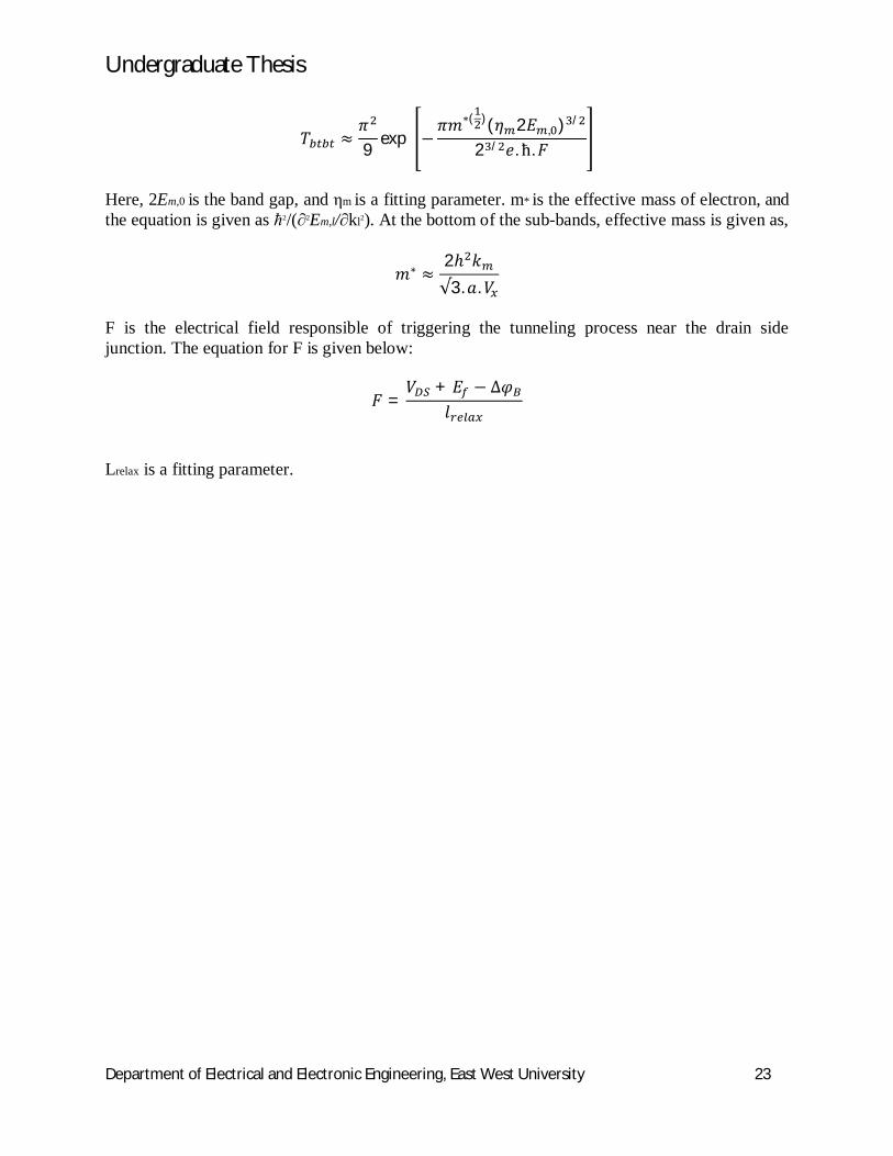
푇 ≈휋9 exp −
휋푚∗( )(휂 2퐸 , ) /
2 / 푒. ћ.퐹
Here, 2Em,0 is the band gap, and ηm is a fitting parameter. m* is the effective mass of electron, and the equation is given as ћ2/(∂2Em,l/∂kl2). At the bottom of the sub-bands, effective mass is given as,
푚∗ ≈2ℎ 푘√3.푎.푉
F is the electrical field responsible of triggering the tunneling process near the drain side junction. The equation for F is given below:
퐹 =푉 + 퐸 − ∆휑
푙
Lrelax is a fitting parameter.

Undergraduate Thesis
Department of Electrical and Electronic Engineering, East West University 24
Chapter 4
Model Implementation
Compact model development in simulators is a difficult work. Most of the simulators essentially depend on accurate model for correct result. As the diversity of simulators increased, complexity of model implementation also increased. Simulator model interfaces require understanding of simulator architecture [16]. Because results of the model depends on simulator architecture. In this chapter we implemented a Verilog-A based accurate compact model for Carbon Nanotube Field Effect Transistors (CNFET) in AGILENT ADS. ADS is a commercial circuit simulator which has excellent architecture for implementing compact model. But the complexity of developing model in ADS environment is difficult to understand for the beginner.
4.1 Why Verilog-A Verilog-A is derivated from IEEE 1364-1995 Verilog HDL and is an IEEE standard analog hardware description language that uses modules to describe the structure and behavior of analog systems. Verilog-A was recently enhanced to provide greater support for compact modeling [17]. In order for Verilog-A to become the standard language for compact model development and implementation, compact model developers must become familiar with the language and simulators must run compact models in Verilog-A as quickly as possible. Below some of the advantages of Verilog-A are described [17]:
Verilog-A modules are compatible with Verilog-AMS HDL. Analog behavioral modeling descriptions are contained in a separate analog block. Branches can be named for easy selection and access. Parameters can be specified with valid range limits. Frees the model developer from the burden of handling the simulator interface. Provides a strong system for defining model parameters.
. The major reason for choosing Verilog-A as a standard language for the compact model is to avoid the need for complex interfaces in the circuit simulators. As the device geometry becomes shorter and shorter physical effects need to be installed into the circuit simulators in a very short time [17]. However, the simulator interface, which includes various functions such as topology checking, parameter reading, current vectors loading, and value initializing presents a significant barrier for model developers. Since Verilog-A is a simulator-independent standard language, the model developers no longer need to deal with these specific details. An important benefit of Verilog-A based compact modeling is that users can access the internal currents, charges, and noise parameters through ADS parameters [18] [19].
Undergraduate Thesis
Department of Electrical and Electronic Engineering, East West University 25
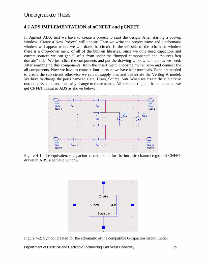
4.2 ADS IMPLEMENTATION of nCNFET and pCNFET In Agilent ADS, first we have to create a project to start the design. After starting a pop-up window “Create a New Project” will appear. Then we write the project name and a schematic window will appear where we will draw the circuit. In the left side of the schematic window there is a drop-down menu of all of the built-in libraries. Since we only need capacitors and current sources we can get all of it from under the “lumped components” and “sources-freq domain” title. We just click the components and put the drawing window as much as we need. After rearranging this components, from the insert menu choosing “wire” icon and connect the all components. Now we have to connect four ports as we have four terminals. Ports are needed to create the sub circuit otherwise we cannot supply bias and instantiate the Verilog-A model. We have to change the ports name to Gate, Drain, Source, Sub. When we create the sub circuit output ports name automatically change to those names. After connecting all the components we get CNFET circuit in ADS as shown below,
Figure 4-1: The equivalent 6-capacitor circuit model for the intrinsic channel region of CNFET drawn in ADS schematic window.
Figure 4-2: Symbol created for the schematic of the compatible 6-capacitor circuit model.

Undergraduate Thesis
Department of Electrical and Electronic Engineering, East West University 26
As our purpose is to model a nCNFET and pCNFET, so we need two different circuits. But for both of them our 6-capacitor circuit model is same except the Verilog-A model. But we have to create two sub circuits because of two different names. To associate a symbol view with above schematic a sub circuit is needed. We use ports to pass signals into and out of the sub circuit. In this schematic from the “View –Create/Edit Schematic Symbol” pull down menu sub circuit can be easily created as shown above Figure 4-2.
After creating the sub circuit we have to configure “design parameter” dialogue box. Under this dialog box we need only “General” tab. Now to instantiate the Verilog-A module through simulator “design parameter” dialog box must be setup as shown in Figure 4-3,
Figure 4-3: Design parameter window in ADS for the symbol containing the internal 6-capacitor circuit model.
Under the “General” tab we change only three entry field- Library Name, Model, Simulate As. To insert the sub circuit in another design “library name” must be given. Then the sub circuit will be added in component list as this library name. As we used built-in component in the circuit that must be written in the model entry point otherwise circuit would not work. Simulate As entry point is filled with Verilog-A code module name “CNT_n” for nCNFET and “CNT_p” for pCNFET to instantiate the code in the circuit. In Agilent ADS, to instantiate the module code must be placed in the project directory. A folder called Verilog-A is created for the current project and the Verilog-A module (va file) was placed in that folder. The Verilog-A module can be instantiated through the simulator. The Verilog-A compiler in ADS, developed by Tiburon Design Automation, then automatically compiles all

Undergraduate Thesis
Department of Electrical and Electronic Engineering, East West University 27
Verilog-A files in the ADS Project Verilog-A folder into simulator. Now we setup simulation and insert sub circuit in the new design window. Here we only show the nCNFET simulation setup because there is no difference between nCNFET and pCNFET circuit design except the Verilog-A code change. In our CNFET device we applied two bias supply, one in drain and another in gate. In gate voltage we applied parameter sweep and in drain voltage dc sweep was applied. As our two voltage supplies are variables we can setup the value by variable component “var”. Voltage source parameter name must be same with the variable component parameter name. Source and sub are shorted. Most importantly in 6-capacitor circuit we cannot interchange the ports name, if changes and voltage supply according to that changes, result would not be as we expected. But if we interchange the Gate and Drain ports then result would not be affected because our both sweep range are same. Both DC sweep and parameter sweep range is from 0 to 1. Gate voltage cannot sweep because parameter sweep does not sweep any parameter itself. Every value of parameter sweep need to be simulated. For that reason simulation controller is included in the parameter sweep. Since we have only DC simulation controller we just put the instance name of DC simulation in “Siminstancename” which is DC1. Now we are ready to simulate the circuit. After clicking the simulate icon we can see the progress of simulation in the hpeesofsim window. Data window where result is drawn will appear after complete simulation. As we want to see the rectangular plot we just click this icon. A plot tracer will appear where our parameters will show. Some parameters appear in format as x.i that means it is a current signal and all others are voltage signal. Now we choose IDS.i vs VDS to see the I-V curve result. I-V curves results are shown in “Result and Discussion”.
Figure 4-4: Simulation setup window for the modeled CNFET with parameter details.

Undergraduate Thesis
Department of Electrical and Electronic Engineering, East West University 28
Chapter 5
Result and Discussion
Here we’ve used ADS as a circuit simulator and advanced ‘VERILOG A’ as the programming language (what we’ve discussed in the previous chapter). We’ve designed two modules: one is for nCNFET and another is for pCNFET with 3 terminals: gate, source & drain. Based on simulation result we have plotted basic characteristic curves for both nCNFET and pCNFET. For this simulation we consider the diameter of the nanotube as 1.5 nm, chirality is (19, 0), 32 nm gate length, 3 nm thick HfO2 (hafnium oxide) as front gate dielectric material and 10 µm thick SiO2 as insulating layer between substrate and the CNT. Our non-idealities include the quantum confinement effects on both circumferential and axial direction, thermionic current, phonon scattering and band to band tunneling current (BTBT). And after simulating with voltage swing in Vgs and Vds by circuit simulator we’ve obtained characteristics curves (Id-Vds) for nMOS and pMOS which are very much acceptable & representing a good device/circuit evaluation.
Figure 5-1: N type CNFET drain current @ (Vgs-varing from 0-1V, VFB=0V) with channel region non-idealities.

Undergraduate Thesis
Department of Electrical and Electronic Engineering, East West University 29
Figure 5-2: P type CNFET drain current @ (Vgs-varing from 0-1V, VFB=0V) with channel region non-idealities.
By inspection of the above two I-V curve we can see on current is about 40 µA and also two conjugative curve difference reduces. Our threshold voltage is 0.4 V. Now, we must discuss about some important points. We can understand that 40 µA on-state current is very much desirable. The amount of current is the proof of high mobility, high current density and high trans-conductance. And not only that, we’re getting an on-state saturated current with a very a low bias voltage (VDS). We all know that the less bias voltage we operate with the less power dissipation will be. Another advantage of low bias voltage operation is reduction of phonon scattering. As bias voltage is low then charge carriers can’t gain as much energy to emit phonons. And with high VDS BTBT (band to band tunneling) reduces the channel current. The drain current we get is pretty much steady in the saturation region. We’re getting no slope in the saturation region. We can see that we’re getting better sub-threshold voltage, better sub-threshold slope and good steady current in saturation region. The gate control and control over channel formation is better. As a result gate delay is reduced. As we used MOSFET like CNFET it can be concluded that both I-V curve shows our expected performance. So, these two curves are verifying our successful ADS implementation of nCNFET and pCNFET.

Undergraduate Thesis
Department of Electrical and Electronic Engineering, East West University 30
Figures 5.1 and 5.2 show intrinsic channel current of nCNFET and pCNFET where we assumed near ballistic or quasi-ballistic one dimensional transport in the channel region. Although all of the factor associated with CNFET contributed to the current but especially thermionic current leads to reduce the channel current. In thermionic current we consider two scattering effect. One is optical phonon other is acoustic phonon scattering. If there were no phonon scattering we would get an on-state current about 42 µA - 43 µA. Optical phonon scattering depends on the carrier energy. A smaller current means a smaller number of high-energy carriers. The current reduction rate with only optical phonon scattering becomes smaller as Lg increases because optical phonon scattering rate decreases as current decreases. Optical phonon scattering is important for short channel device due to its short mean free path (MFP) (~15nm). Acoustic phonon scattering with longer MFP (~500nm) is important if Lg increases as the acoustic phonon energy is small and therefore acoustic phonon scattering has a weak dependence on the carrier energy. For short channel device Acoustic phonon scattering has not much role. BTBT current only significant with high Vds bias. Now we’ll discuss about scattering effect on channel resistance. The total channel dc resistance can be written as Rtot=Rideal+ΔR, where Rideal is the quantum resistance which is a function of the band-structure with ballistic transport, and ΔR denotes the additional resistance contributed by phonon scattering. Rideal is almost constant in the saturation region. Acoustic phonon scattering weakly depends on carrier energy, thus acoustic phonon scattering induced ΔR is almost constant in the saturation region. A constant linear channel resistance approximation is only valid with small bias where optical phonon scattering is not significant. Optical phonon scattering increases as bias increases due to more high-energy carriers. Therefore optical phonon scattering induced ΔR increases with bias Vdd.

Undergraduate Thesis
Department of Electrical and Electronic Engineering, East West University 31
CONCLUSION In this thesis work, our main purpose was ADS implementation of a 6-capacitor compact model of a carbon nanotube transistor proposed by J. Deng and H.-S P. Wong. The model includes phonon scattering and band to band tunneling current. We worked with Advanced Design System (ADS) as circuit simulator and the simulator code is written in Verilog-A. By using ADS internal components we designed the internal circuit for nCNFET and pCNFET and we converted the circuit into a 4-terminal (drain, gate, source and substrate) transistor symbol. After that we applied bias and performed DC operation to get their characteristic curves. To do that we had to link the internal transistor circuit with the code written in Verilog-A. The code is verified by simulating the I-V characteristics of n-channel and p-channel CNFETs. ADS is the world’s leading electronic design automation software. ADS is being used in the most innovative and commercially successful technologies. And Verilog-A as a simulator language is becoming very much popular in industrial implementations day by day.
FUTURE WORK As a compact model further improvement in this implemented model is required for improving the accuracy. This model utilizes a simplified band structure which requires high power supply and high surface potential. A more complete tight binding model can reduce this issue. Higher current caused by holes (electron) reserved in the nCNFET (pCNFET) in the cannel region should be considered. The diffusion capacitances due to minority carriers at the source/drain junctions are ignored. It should be considered for the high frequency analog circuit. The effect of CNT defect on device performance as a function of bias should be considered. More sub bands and sub states must be added to get an accurate result at the cost of longer run time. Though CNT device performance cannot compete with well developed CMOS but CNT still remains an attractive material for nano scale devices.

Undergraduate Thesis
Department of Electrical and Electronic Engineering, East West University 32
REFERENCES [1] Data from http://www.itrs.net/Links/2005ITRS/Home2005.htm [2] J. Kedzierski, P. Xuan, E.H. Anderson, J. Bokor, T-J. King, C. Hu, “Complementary silicide source/drain thin-body MOSFETs for the 20 nm gate length regime,” IEDM, pp. 57-60, 2000. [3] Jie Deng,“Device Modeling and Circuit Performance Evaluation for Nanoscale Devices: Silicon Technology beyond 45 nm node and Carbon Nanotube Field Effect Transistor,” PhD dissertation, Stanford University, 2007. [4] R. Saito, G. Dresselhaus, and M. S. Dresselhaus, “Physical Properties of Carbon Nanotubes,” Imperial College Press, London, pp. 272, 978-1-86094-379-9, 1998. [5] J. W. Mintmire and C. T. White, “Universal Density of States for Carbon Nanotubes,” Physical Review Letters, vol. 81, pp. 2506-2509, 1998. [6] A. Javey, J. Guo, D. B. Farmer, Q. Wang, D. Wang, R. G. Gordon, M. Lundstrom, and H. Dai, “Carbon Nanotube Field-Effect Transistors with Integrated Ohmic Contacts and High-k Gate Dielectrics,” Nano Letters, vol. 4, pp. 447-450, 2004. [7] D. Mann, A. Javey, J. Kong, Q. Wang, and H. Dai, “Ballistic Transport in Metallic Nanotubes with Reliable Pd Ohmic Contacts,” Nano Letters, vol. 3, pp. 1541-1544, 2003. [8] J. Deng and H.-S P. Wong, “A Compact SPICE Model for Carbon Nanotube Field Effect Transistors Including Non-Idealities and Its Application — Part I: Model of the Intrinsic Channel Region.” IEEE Transactions on Electron Devices, vol. 54, pp. 3186-3194, 2007. [9] K. Natori, Y. Kimura, and T. Shimizu, “Characteristics of a Carbon Nanotube Field-Effect Transistor Analyzed as a Ballistic Nanowire Field-Effect Transistor,” Journal of Applied Physics, vol. 97, pp. 034306, 2005. [10] J. Guo, M. Lundstrom, and S. Datta, “Performance Projections for Ballistic Carbon Nanotube Field-Effect Transistors,” Applied Physics Letters, vol. 80, pp.3192-3194, 2002. [11] A. Raychowdhury, S. Mukhopadhyay, and K. Roy, “A Circuit-Compatible Model of Ballistic Carbon Nanotube Field-Effect Transistors,” IEEE Transactions on Computer-Aided Design of Integrated Circuits and Systems, vol. 23, pp. 1411-1420, 2006. [12] J. Guo and M. Lundstrom, "Role of Phonon Scattering In Carbon Nanotube Field-Effect Transistors," Applied Physics Letters, vol. 86, pp. 193103, 2005. [13]Francois Leonard,“The Physics of Carbon Nanotubes Devices,” William Andrew Inc, Norwich, NY, 1st Edition, pp. 310, 978-0-8155-1573-9, 2009. [14] J. Geist, J. R. Lowney, “Effect of Band-Gap Narrowing On the Build-In Electrical Field In n-type Silicon,” Journal of Applied Physics, vol. 52, pp. 1121-1123, 1981. [15] A. Naeemi and J. D. Meindl, "Impact of Electron-Phonon Scattering On the Performance of Carbon Nanotube Interconnects for GSI," Electron Device Letters, IEEE, vol. 26, pp. 476-478, 2005. [16] M. Mierzwinski, P. O’Halloran, B. Troyanovsky, R. Dutton, “Changing the Paradigm for Compact Model Integration in Circuit Simulators Using Verilog-A,” Technical Proceedings of the Nanotechnology Conference and Trade Show, vol. 2, pp. 376-379, 2003. [17] Geoffrey J. Coram, “How to write a compact model in Verilog-A,” IEEE International Behavioral Modeling and Simulation Conference, 2004. [18] Guide to Agilent’s Advanced Design System (ADS), Montana State University, 2008. [19] Advanced Design System tutorial, Agilent Technologies, Santa Clara, CA, 2009. [20] Verilog-A Language Reference Manual, Version 1.0, Open Verilog International, 1996.

Undergraduate Thesis
Department of Electrical and Electronic Engineering, East West University 33
APPENDIX Both nCNFET and pCNFET Verilog-A model has given below with full list parameters value. Vams file for parameter (parameters.vams) `define TEMP 27.0 // Temperature of operation /Natural Constants: Do not change/ `define q 1.60e-19 // Electronic charge `define Vpi 3.033 // The carbon PI-PI bond energy `define d 0.144e-9 // The carbon PI-PI bond distance `define a 0.2495e-9 // The carbon atom distance `define pi 3.1416 // PI, constant `define h 6.63e-14 // Planck constant,X1e20 `define h_ba 1.0552e-14 // h_bar, X1e20 `define k 8.617e-5 // Boltzmann constant `define epso 8.85e-12 // Dielectric constant in vacuum `define kT (`k*(`TEMP+273)) // The KT constant `define L_channel 22.0e-9 // CNFET printed/physical channel length, assume 32nm for 32nm node technology `define Lceff 200.0e-9 // The mean free path in intrinsic CNT, estimated as 200nm `define L_sd 22.0e-9 // n+CNT source/drain full length, 32nm, from gate edge to S/D metal contact edge `define Efo 0.6 // The n+/p+ doped CNT fermi level (eV), 0.66eV for 1% doping level, 0.6eV for 0.8% doping level `define Kox 16.0 // The dielectric constant of high-K gate oxide `define Ccsd 0.0e-12 // The coupling capacitance between channel region and source/drain islands `define CoupleRatio 0.0 // The percentage of coupling capacitance between channel and drain out of the total fringe capacitance Ccsd `define sub_pitch 6.4e-9 // Sublithographic pitch (e.g. for CNT gate), 6.4nm `define Klowk 2.0 // The dielectric constant of low-k material `define Ksub 4.0 // The dielectric constant of SiO2 `define Ld_par 15.0e-9 // Length of the drain CNT,1 MFP of OP scattering, to calculate parasitic diffusion capacitance `define lambda_op 15.0e-9 // The Optical Phonon backscattering mean-free-path with Metallic CNT,15nm `define lambda_ap 500.0e-9 // The Acoustic Phonon backscattering mean-free-path with Metallic CNT, 500nm `define photon 0.16 // The photon energy, typical value 0.16eV `define L_relax 40.0e-9 // delta_Vds relaxation range at drain side, fitting parameter

Undergraduate Thesis
Department of Electrical and Electronic Engineering, East West University 34
`define Leff 15.0e-9 // The mean free path in p+/n+ doped CNT, estimated as 15nm `define phi_M 4.6 // Metal workfunction `define phi_S 4.5 // CNT workfunction `define Cgsub 30e-12 // Metal gate (W) to Substrate fringe capacitance per unit length,approximated as 30af/um, with 10um thick Si02 `define Cgabove 27e-12 // W local interconnect to M1 coupling capacitance, 500nm apart, infinite large plane `define Cc_cnt 26e-12 // The coupling capacitance between CNTs with 2Fs=6.4nm, about 26pF/m `define Ccabove 15e-12 // Coupling capacitance between CNT and the above M1 layer, 500nm apart `define Cc_gate 78e-12 // The coupling capacitance between gates with 2F=64nm, about 78pF/m, W=32nm, H=64nm, contact spacing 32nm `define Ctot (`Cgsub+`Cgabove+`Cc_gate+`Cc_gate) // total coupling capacitance for gate region `define Cint (0*`Cc_cnt+0.5*(`Cgsub+`Ccabove)) // total coupling capacitance for source/drain region CNT, redefined within models `define Coeff1_Cgsd 10.54e-12 // The slope for Cg_sd vs. Lsd, H=64nm, Klowk=2, contact spacing 32nm, valid for 10nm<Lsd<100nm `define Coeff2_Cgsd 0.28e-18 //The intersection of Cg_sd vs. Lsd, H=64nm, Klowk=2, contact spacing 32nm, valid for 10nm<Lsd<100nm `define Rsub 1.0 // Substrate resistance, set to zero for the ideal case `define Rcnt 3.3e3 // n+ CNT resistance due to finite modes, 3.3K for 0.7eV doped n+CNT `define FacR 0.4 // The factor of Rus/Rcnt `define de_fac 4.0 // the factor to calculate the number of electrons in CNT `define Lgmax 100.0e-9 // The maximum channel length to calculate current for short channel device `define coeffj (4*`q/`h*`q/1e-20) // The coefficient of current component, 4 is due to both spin degeneracy and mode degeneracy `define Coeff_Cc (`pi*`Klowk*`epso) // The coefficient of the coupling capacitance between adjacent CNTs `define Rus (`Rcnt*`FacR) // Source side contact resistance `define Rud (`Rcnt*(1-`FacR)) // Drain side contact resistance

Undergraduate Thesis
Department of Electrical and Electronic Engineering, East West University 35
nCNFET and pCNFET Verilog-A file `include "disciplines.vams" `include "parameters.vams" module CNT_n(Drain, Gate, Source, Sub); //Input variables definitions parameter real Lg=`L_channel; parameter real Lgeff=`Lceff; parameter real Lss=`L_sd; parameter real Ldd=`L_sd; parameter real Efi=`Efo; parameter real Kgate=`Kox; parameter real Tox=4.0e-9; parameter real Csub=20.0e-12; parameter real Ccsd=0.0; parameter real CoupleRatio=0.0; parameter real Vfbn=0.0; parameter real GF=0.0; parameter real Pitch=20.0e-9; parameter real n1=19 ; parameter real n2=0.0; parameter real CNTPos=1.0; // Electrical connections inout Drain, Gate, Source, Sub; electrical Drain, Gate, Source, Sub, Gs; /******************************************** ****** A. The Gate-CNT coupling capacitance * ********************************************/ //Csub is CNT to Substrate capacitance per unit length,approximated as 20af/um with 10um thick SiO2, 40af/um with 130nm thick SiO2 real Lgate; // If Lg>Lgmax, Lgate= Lgmax to approximate the long channel device current real dia; // The diameter of the CNT real rad; // The radius of the CNT real Hei; // Oxide thickness real RCo; // The inverse of the capacitance with the uniform Kgate dielectric material real RCimg; // The inverse of the effects due to the image charge real RCinf; // The inverse of the capacitance with infinite spacing between CNTs real Vadjc; // The potential by the adjacent CNT real Vadji; // The potential by the image charge of the adjacent CNT real RCadj; // The total potential contributed by the adjacent CNT and its image charge real beta; // The ratio of image charge over real charge real Cprefactor; // Capacitance pre-factor real Cedge; // The gate to EdgeCNT coupling capacitance real Cmid; // The gate to MidCnt coupling capacitance

Undergraduate Thesis
Department of Electrical and Electronic Engineering, East West University 36
real Ci; // The gate capacitance, Cedge if CNTPos=1, Cmid if CNTPos=0 real Cc; // The coupling capacitance between the channel region of the CNT to the doped source/drain region of another CNT real Csub_tot; // The total coupling capacitance between the channel region of one CNT and the substrate, as well as source/drain islands real Cratio; // The ratio between actual gate capcitance and ideal gate capacitance real Lcc; real Lcb; real Cqd; real Cqs; /********************************************************************************** ****** B. The E-K disperation relationship, linear approximation around Ef point ** **********************************************************************************/ // The E-K disperation relationship, linear approximation around Ef point real K1; // The first perpendicular wave number real K2; // The second perpendicular wave number // The parallel wave number real Kp1, Kp2, Kp3, Kp4, Kp5, Kp6, Kp7, Kp8, Kp9; // The energy of the (m,n)th sub-band, above Ei real CoeffE; real E11, E12, E13, E14, E15, E16, E17, E18, E19; real E21, E22, E23, E24, E25, E26, E27, E28, E29; // Energy of the perpendicular component of the mth sub-band, above Ei real E1, E2; // The kinetic energy of the mth sub-band real En11, En12, En13, En14, En15, En16, En17, En18, En19; real En21, En22, En23, En24, En25, En26, En27, En28, En29; // The coefficients of Jmn real CocoJ, delta_phib; real Coeff_J11, Coeff_J12, Coeff_J13, Coeff_J14, Coeff_J15, Coeff_J16, Coeff_J17, Coeff_J18, Coeff_J19; real Coeff_J21, Coeff_J22, Coeff_J23, Coeff_J24, Coeff_J25, Coeff_J26, Coeff_J27, Coeff_J28, Coeff_J29; /************************************************************************** *** C.The carrier effective mass of the 1st and the 2nd subband for CNT *** **************************************************************************/ real meff1, meff2; /************************************************************************ ************* D. Component values to be computed heavily **************** ************************************************************************/ real Gcnt; real Gbtbt; real Cdj;

Undergraduate Thesis
Department of Electrical and Electronic Engineering, East West University 37
/***************************************************************/ analog begin begin // Assign basic parameters Lgate = min(Lg,`Lgmax); dia = `a*sqrt(pow(n1,2)+n1*n2+pow(n2,2))/`pi; rad = dia/2; Hei = Tox+rad; RCo = ln(2*Hei/dia+sqrt(pow(2*Hei/dia,2)-1)); beta = (Kgate-`Ksub)/(Kgate+`Ksub); RCimg = beta*ln(2*Hei/(3*dia)+2.0/3.0); RCinf = RCo+RCimg; Vadjc=0.5*ln((pow(Pitch,2)+2*(Hei-rad)*(Hei+sqrt(pow(Hei,2)-pow(rad,2))))/(pow(Pitch,2)+2*(Hei-rad)*(Hei-sqrt(pow(Hei,2)-pow(rad,2))))); Vadji =0.5*beta*ln((pow(Hei+dia,2)+pow(Pitch,2))/(9*pow(rad,2)+pow(Pitch,2)))*tanh((Hei+rad)/(Pitch-dia)); RCadj = Vadjc+Vadji; Cprefactor = 2*`pi*Kgate*`epso; Cedge = Cprefactor/(RCinf+RCadj); Cmid = 2*Cedge-Cprefactor/RCinf; Ci = Cedge*CNTPos+Cmid*(1-CNTPos); Cc = (Cedge/Cmid-1)*Cedge*ln(2*Pitch/dia)/ln(Pitch/dia+sqrt(pow(Pitch/dia,2)-1)); Csub_tot = Csub + `Ccsd; Cratio = Ci*RCinf/Cprefactor; Lcc = beta*Cc; Lcb = (1-beta)*Cc; delta_phib=0.6e-19; K1 = 2*`pi/(3*`a*sqrt(pow(n1,2)+n1*n2+pow(n2,2))); K2 = 2*K1; Kp1=2*`pi/Lgate; Kp2=2*Kp1; Kp3=3*Kp1; Kp4=4*Kp1; Kp5=5*Kp1; Kp6=6*Kp1; Kp7=7*Kp1; Kp8=8*Kp1; Kp9=9*Kp1; E1 = `Vpi*`pi/sqrt(3.0*(pow(n1,2)+n1*n2+pow(n2,2))); E2 = 2*E1; CoeffE = sqrt(3.0)/2.0*`a*`Vpi; E11 = CoeffE*sqrt(pow(K1,2)+pow(Kp1,2)); E12 = CoeffE*sqrt(pow(K1,2)+pow(Kp2,2)); E13 = CoeffE*sqrt(pow(K1,2)+pow(Kp3,2));

Undergraduate Thesis
Department of Electrical and Electronic Engineering, East West University 38
E14 = CoeffE*sqrt(pow(K1,2)+pow(Kp4,2)); E15 = CoeffE*sqrt(pow(K1,2)+pow(Kp5,2)); E16 = CoeffE*sqrt(pow(K1,2)+pow(Kp6,2)); E17 = CoeffE*sqrt(pow(K1,2)+pow(Kp7,2)); E18 = CoeffE*sqrt(pow(K1,2)+pow(Kp8,2)); E19 = CoeffE*sqrt(pow(K1,2)+pow(Kp9,2)); E21 = CoeffE*sqrt(pow(K2,2)+pow(Kp1,2)); E22 = CoeffE*sqrt(pow(K2,2)+pow(Kp2,2)); E23 = CoeffE*sqrt(pow(K2,2)+pow(Kp3,2)); E24 = CoeffE*sqrt(pow(K2,2)+pow(Kp4,2)); E25 = CoeffE*sqrt(pow(K2,2)+pow(Kp5,2)); E26 = CoeffE*sqrt(pow(K2,2)+pow(Kp6,2)); E27 = CoeffE*sqrt(pow(K2,2)+pow(Kp7,2)); E28 = CoeffE*sqrt(pow(K2,2)+pow(Kp8,2)); E29 = CoeffE*sqrt(pow(K2,2)+pow(Kp9,2)); En11 = E11 - E1; En12 = E12 - E1; En13 = E13 - E1; En14 = E14 - E1; En15 = E15 - E1; En16 = E16 - E1; En17 = E17 - E1; En18 = E18 - E1; En19 = E19 - E1; En21 = E21 - E2; En22 = E22 - E2; En23 = E23 - E2; En24 = E24 - E2; En25 = E25 - E2; En26 = E26 - E2; En27 = E27 - E2; En28 = E28 - E2; En29 = E29 - E2; CocoJ = sqrt(3.0)*`a*`pi*`Vpi; Coeff_J11 = Kp1/sqrt(pow(K1,2)+pow(Kp1,2)); Coeff_J12 = Kp2/sqrt(pow(K1,2)+pow(Kp2,2)); Coeff_J13 = Kp3/sqrt(pow(K1,2)+pow(Kp3,2)); Coeff_J14 = Kp4/sqrt(pow(K1,2)+pow(Kp4,2)); Coeff_J15 = Kp5/sqrt(pow(K1,2)+pow(Kp5,2)); Coeff_J16 = Kp6/sqrt(pow(K1,2)+pow(Kp6,2)); Coeff_J17 = Kp7/sqrt(pow(K1,2)+pow(Kp7,2)); Coeff_J18 = Kp8/sqrt(pow(K1,2)+pow(Kp8,2)); Coeff_J19 = Kp9/sqrt(pow(K1,2)+pow(Kp9,2));

Undergraduate Thesis
Department of Electrical and Electronic Engineering, East West University 39
Coeff_J21 = Kp1/sqrt(pow(K2,2)+pow(Kp1,2)); Coeff_J22 = Kp2/sqrt(pow(K2,2)+pow(Kp2,2)); Coeff_J23 = Kp3/sqrt(pow(K2,2)+pow(Kp3,2)); Coeff_J24 = Kp4/sqrt(pow(K2,2)+pow(Kp4,2)); Coeff_J25 = Kp5/sqrt(pow(K2,2)+pow(Kp5,2)); Coeff_J26 = Kp6/sqrt(pow(K2,2)+pow(Kp6,2)); Coeff_J27 = Kp7/sqrt(pow(K2,2)+pow(Kp7,2)); Coeff_J28 = Kp8/sqrt(pow(K2,2)+pow(Kp8,2)); Coeff_J29 = Kp9/sqrt(pow(K2,2)+pow(Kp9,2)); meff1 = 2*`h_ba*`h_ba*K1/(sqrt(3.0)*`a*`q*`Vpi)/1.0e40; meff2 = 2*`h_ba*`h_ba*K2/(sqrt(3.0)*`a*`q*`Vpi)/1.0e40; end // End: Assign basic parameters begin : evaluate_Gcnt real vds, offset; real current_sub_1, current_sub_2; real current_sub11; real current_sub12, current_sub13, current_sub14, current_sub15; real current_sub16, current_sub17, current_sub18, current_sub19; real current_sub21; real current_sub22, current_sub23, current_sub24, current_sub25; real current_sub26, current_sub27, current_sub28, current_sub29; real T11, T12, T13, T14, T15, T16, T17, T18, T19; real T21, T22, T23, T24, T25, T26, T27, T28, T29; real T11_0, T12_0, T13_0, T14_0, T15_0, T16_0, T17_0, T18_0, T19_0; real T21_0, T22_0, T23_0, T24_0, T25_0, T26_0, T27_0, T28_0, T29_0; real fermi_s11; real fermi_s12, fermi_s13, fermi_s14, fermi_s15; real fermi_s16, fermi_s17, fermi_s18, fermi_s19; real fermi_s21; real fermi_s22, fermi_s23, fermi_s24, fermi_s25; real fermi_s26, fermi_s27, fermi_s28, fermi_s29; real fermi_d11; real fermi_d12, fermi_d13, fermi_d14, fermi_d15; real fermi_d16, fermi_d17, fermi_d18, fermi_d19; real fermi_d21; real fermi_d22, fermi_d23, fermi_d24, fermi_d25; real fermi_d26, fermi_d27, fermi_d28, fermi_d29; real l_op11, l_op12, l_op13, l_op14, l_op15, l_op16, l_op17, l_op18, l_op19; real l_op21, l_op22, l_op23, l_op24, l_op25, l_op26, l_op27, l_op28, l_op29; real l_op11_0, l_op12_0, l_op13_0, l_op14_0, l_op15_0, l_op16_0, l_op17_0, l_op18_0, l_op19_0; real l_op21_0, l_op22_0, l_op23_0, l_op24_0, l_op25_0, l_op26_0, l_op27_0, l_op28_0, l_op29_0; real FDOS11, FDOS12, FDOS13, FDOS14, FDOS15, FDOS16, FDOS17, FDOS18, FDOS19; real FDOS21, FDOS22, FDOS23, FDOS24, FDOS25, FDOS26, FDOS27, FDOS28, FDOS29; realfermi_op11,fermi_op12,fermi_op13,fermi_op14,fermi_op15,fermi_op16,fermi_op17,fermi_op18,fermi_op19;

Undergraduate Thesis
Department of Electrical and Electronic Engineering, East West University 40
realfermi_op21,fermi_op22,fermi_op23,fermi_op24,fermi_op25,fermi_op26,fermi_op27,fermi_op28,fermi_op29; realfermi_op11_0,fermi_op12_0,fermi_op13_0,fermi_op14_0,fermi_op15_0,fermi_op16_0,fermi_op17_0,fermi_op18_0,fermi_op19_0; realfermi_op21_0,fermi_op22_0,fermi_op23_0,fermi_op24_0,fermi_op25_0,fermi_op26_0,fermi_op27_0,fermi_op28_0,fermi_op29_0; // Parameters passing along vds = V(Drain,Source); offset = `photon; // Evalute fermi_sxx and fermi_dxx fermi_s11 = 1.0/(1.0+limexp((E11-delta_phib)/`kT)); fermi_s12 = 1.0/(1.0+limexp((E12-delta_phib)/`kT)); fermi_s13 = 1.0/(1.0+limexp((E13-delta_phib)/`kT)); fermi_s14 = 1.0/(1.0+limexp((E14-delta_phib)/`kT)); fermi_s15 = 1.0/(1.0+limexp((E15-delta_phib)/`kT)); fermi_s16 = 1.0/(1.0+limexp((E16-delta_phib)/`kT)); fermi_s17 = 1.0/(1.0+limexp((E17-delta_phib)/`kT)); fermi_s18 = 1.0/(1.0+limexp((E18-delta_phib)/`kT)); fermi_s19 = 1.0/(1.0+limexp((E19-delta_phib)/`kT)); fermi_s21 = 1.0/(1.0+limexp((E21-delta_phib)/`kT)); fermi_s22 = 1.0/(1.0+limexp((E22-delta_phib)/`kT)); fermi_s23 = 1.0/(1.0+limexp((E23-delta_phib)/`kT)); fermi_s24 = 1.0/(1.0+limexp((E24-delta_phib)/`kT)); fermi_s25 = 1.0/(1.0+limexp((E25-delta_phib)/`kT)); fermi_s26 = 1.0/(1.0+limexp((E26-delta_phib)/`kT)); fermi_s27 = 1.0/(1.0+limexp((E27-delta_phib)/`kT)); fermi_s28 = 1.0/(1.0+limexp((E28-delta_phib)/`kT)); fermi_s29 = 1.0/(1.0+limexp((E29-delta_phib)/`kT)); fermi_d11 = limexp(-vds/`kT)/(limexp(-vds/`kT)+limexp((E11-delta_phib)/`kT)); fermi_d12 = limexp(-vds/`kT)/(limexp(-vds/`kT)+limexp((E12-delta_phib)/`kT)); fermi_d13 = limexp(-vds/`kT)/(limexp(-vds/`kT)+limexp((E13-delta_phib)/`kT)); fermi_d14 = limexp(-vds/`kT)/(limexp(-vds/`kT)+limexp((E14-delta_phib)/`kT)); fermi_d15 = limexp(-vds/`kT)/(limexp(-vds/`kT)+limexp((E15-delta_phib)/`kT)); fermi_d16 = limexp(-vds/`kT)/(limexp(-vds/`kT)+limexp((E16-delta_phib)/`kT)); fermi_d17 = limexp(-vds/`kT)/(limexp(-vds/`kT)+limexp((E17-delta_phib)/`kT)); fermi_d18 = limexp(-vds/`kT)/(limexp(-vds/`kT)+limexp((E18-delta_phib)/`kT)); fermi_d19 = limexp(-vds/`kT)/(limexp(-vds/`kT)+limexp((E19-delta_phib)/`kT)); fermi_d21 = limexp(-vds/`kT)/(limexp(-vds/`kT)+limexp((E21-delta_phib)/`kT)); fermi_d22 = limexp(-vds/`kT)/(limexp(-vds/`kT)+limexp((E22-delta_phib)/`kT)); fermi_d23 = limexp(-vds/`kT)/(limexp(-vds/`kT)+limexp((E23-delta_phib)/`kT)); fermi_d24 = limexp(-vds/`kT)/(limexp(-vds/`kT)+limexp((E24-delta_phib)/`kT)); fermi_d25 = limexp(-vds/`kT)/(limexp(-vds/`kT)+limexp((E25-delta_phib)/`kT)); fermi_d26 = limexp(-vds/`kT)/(limexp(-vds/`kT)+limexp((E26-delta_phib)/`kT));

Undergraduate Thesis
Department of Electrical and Electronic Engineering, East West University 41
fermi_d27 = limexp(-vds/`kT)/(limexp(-vds/`kT)+limexp((E27-delta_phib)/`kT)); fermi_d28 = limexp(-vds/`kT)/(limexp(-vds/`kT)+limexp((E28-delta_phib)/`kT)); fermi_d29 = limexp(-vds/`kT)/(limexp(-vds/`kT)+limexp((E29-delta_phib)/`kT)); // Evaluate FDOSXX FDOS11 = (E11-offset)/sqrt(abs(pow((E11-offset),2)-pow(E1,2)))*max(En11-offset,1.0e-14); FDOS12 = (E12-offset)/sqrt(abs(pow((E12-offset),2)-pow(E1,2)))*max(En12-offset,1.0e-14); FDOS13 = (E13-offset)/sqrt(abs(pow((E13-offset),2)-pow(E1,2)))*max(En13-offset,1.0e-14); FDOS14 = (E14-offset)/sqrt(abs(pow((E14-offset),2)-pow(E1,2)))*max(En14-offset,1.0e-14); FDOS15 = (E15-offset)/sqrt(abs(pow((E15-offset),2)-pow(E1,2)))*max(En15-offset,1.0e-14); FDOS16 = (E16-offset)/sqrt(abs(pow((E16-offset),2)-pow(E1,2)))*max(En16-offset,1.0e-14); FDOS17 = (E17-offset)/sqrt(abs(pow((E17-offset),2)-pow(E1,2)))*max(En17-offset,1.0e-14); FDOS18 = (E18-offset)/sqrt(abs(pow((E18-offset),2)-pow(E1,2)))*max(En18-offset,1.0e-14); FDOS19 = (E19-offset)/sqrt(abs(pow((E19-offset),2)-pow(E1,2)))*max(En19-offset,1.0e-14); FDOS21 = (E21-offset)/sqrt(abs(pow((E21-offset),2)-pow(E2,2)))*max(En21-offset,1.0e-14); FDOS22 = (E22-offset)/sqrt(abs(pow((E22-offset),2)-pow(E2,2)))*max(En22-offset,1.0e-14); FDOS23 = (E23-offset)/sqrt(abs(pow((E23-offset),2)-pow(E2,2)))*max(En23-offset,1.0e-14); FDOS24 = (E24-offset)/sqrt(abs(pow((E24-offset),2)-pow(E2,2)))*max(En24-offset,1.0e-14); FDOS25 = (E25-offset)/sqrt(abs(pow((E25-offset),2)-pow(E2,2)))*max(En25-offset,1.0e-14); FDOS26 = (E26-offset)/sqrt(abs(pow((E26-offset),2)-pow(E2,2)))*max(En26-offset,1.0e-14); FDOS27 = (E27-offset)/sqrt(abs(pow((E27-offset),2)-pow(E2,2)))*max(En27-offset,1.0e-14); FDOS28 = (E28-offset)/sqrt(abs(pow((E28-offset),2)-pow(E2,2)))*max(En28-offset,1.0e-14); FDOS29 = (E29-offset)/sqrt(abs(pow((E29-offset),2)-pow(E2,2)))*max(En29-offset,1.0e-14); // Evaluate T1X, T2X (with nonzero vds) // Evaluate fermi_opxx fermi_op11 = limexp((offset-vds)/`kT)/(limexp((offset-vds)/`kT)+limexp((E11-delta_phib)/`kT)); fermi_op12 = limexp((offset-vds)/`kT)/(limexp((offset-vds)/`kT)+limexp((E12-delta_phib)/`kT)); fermi_op13 = limexp((offset-vds)/`kT)/(limexp((offset-vds)/`kT)+limexp((E13-delta_phib)/`kT)); fermi_op14 = limexp((offset-vds)/`kT)/(limexp((offset-vds)/`kT)+limexp((E14-delta_phib)/`kT)); fermi_op15 = limexp((offset-vds)/`kT)/(limexp((offset-vds)/`kT)+limexp((E15-delta_phib)/`kT)); fermi_op16 = limexp((offset-vds)/`kT)/(limexp((offset-vds)/`kT)+limexp((E16-delta_phib)/`kT)); fermi_op17 = limexp((offset-vds)/`kT)/(limexp((offset-vds)/`kT)+limexp((E17-delta_phib)/`kT)); fermi_op18 = limexp((offset-vds)/`kT)/(limexp((offset-vds)/`kT)+limexp((E18-delta_phib)/`kT)); fermi_op19 = limexp((offset-vds)/`kT)/(limexp((offset-vds)/`kT)+limexp((E19-delta_phib)/`kT)); fermi_op21 = limexp((offset-vds)/`kT)/(limexp((offset-vds)/`kT)+limexp((E21-delta_phib)/`kT)); fermi_op22 = limexp((offset-vds)/`kT)/(limexp((offset-vds)/`kT)+limexp((E22-delta_phib)/`kT)); fermi_op23 = limexp((offset-vds)/`kT)/(limexp((offset-vds)/`kT)+limexp((E23-delta_phib)/`kT)); fermi_op24 = limexp((offset-vds)/`kT)/(limexp((offset-vds)/`kT)+limexp((E24-delta_phib)/`kT)); fermi_op25 = limexp((offset-vds)/`kT)/(limexp((offset-vds)/`kT)+limexp((E25-delta_phib)/`kT)); fermi_op26 = limexp((offset-vds)/`kT)/(limexp((offset-vds)/`kT)+limexp((E26-delta_phib)/`kT)); fermi_op27 = limexp((offset-vds)/`kT)/(limexp((offset-vds)/`kT)+limexp((E27-delta_phib)/`kT)); fermi_op28 = limexp((offset-vds)/`kT)/(limexp((offset-vds)/`kT)+limexp((E28-delta_phib)/`kT)); fermi_op29 = limexp((offset-vds)/`kT)/(limexp((offset-vds)/`kT)+limexp((E29-delta_phib)/`kT));

Undergraduate Thesis
Department of Electrical and Electronic Engineering, East West University 42
// Evaluate l_op1x and l_op2x l_op11 = `lambda_op/(FDOS11*(1-fermi_op11)); l_op12 = `lambda_op/(FDOS12*(1-fermi_op12)); l_op13 = `lambda_op/(FDOS13*(1-fermi_op13)); l_op14 = `lambda_op/(FDOS14*(1-fermi_op14)); l_op15 = `lambda_op/(FDOS15*(1-fermi_op15)); l_op16 = `lambda_op/(FDOS16*(1-fermi_op16)); l_op17 = `lambda_op/(FDOS17*(1-fermi_op17)); l_op18 = `lambda_op/(FDOS18*(1-fermi_op18)); l_op19 = `lambda_op/(FDOS19*(1-fermi_op19)); l_op21 = `lambda_op/(FDOS21*(1-fermi_op21)); l_op22 = `lambda_op/(FDOS22*(1-fermi_op22)); l_op23 = `lambda_op/(FDOS23*(1-fermi_op23)); l_op24 = `lambda_op/(FDOS24*(1-fermi_op24)); l_op25 = `lambda_op/(FDOS25*(1-fermi_op25)); l_op26 = `lambda_op/(FDOS26*(1-fermi_op26)); l_op27 = `lambda_op/(FDOS27*(1-fermi_op27)); l_op28 = `lambda_op/(FDOS28*(1-fermi_op28)); l_op29 = `lambda_op/(FDOS29*(1-fermi_op29)); T11 = 1.0/(1.0+Lg/l_op11); T12 = 1.0/(1.0+Lg/l_op12); T13 = 1.0/(1.0+Lg/l_op13); T14 = 1.0/(1.0+Lg/l_op14); T15 = 1.0/(1.0+Lg/l_op15); T16 = 1.0/(1.0+Lg/l_op16); T17 = 1.0/(1.0+Lg/l_op17); T18 = 1.0/(1.0+Lg/l_op18); T19 = 1.0/(1.0+Lg/l_op19); T21 = 1.0/(1.0+Lg/l_op21); T22 = 1.0/(1.0+Lg/l_op22); T23 = 1.0/(1.0+Lg/l_op23); T24 = 1.0/(1.0+Lg/l_op24); T25 = 1.0/(1.0+Lg/l_op25); T26 = 1.0/(1.0+Lg/l_op26); T27 = 1.0/(1.0+Lg/l_op27); T28 = 1.0/(1.0+Lg/l_op28); T29 = 1.0/(1.0+Lg/l_op29); // Evaluate T1X_0, T2X_0 (with zero vds) // Evaluate fermi_opxx_0 (with zero vds) fermi_op11_0 = limexp((offset-0.0)/`kT)/(limexp((offset-0.0)/`kT)+limexp((E11-delta_phib)/`kT)); fermi_op12_0 = limexp((offset-0.0)/`kT)/(limexp((offset-0.0)/`kT)+limexp((E12-delta_phib)/`kT)); fermi_op13_0 = limexp((offset-0.0)/`kT)/(limexp((offset-0.0)/`kT)+limexp((E13-delta_phib)/`kT)); fermi_op14_0 = limexp((offset-0.0)/`kT)/(limexp((offset-0.0)/`kT)+limexp((E14-delta_phib)/`kT)); fermi_op15_0 = limexp((offset-0.0)/`kT)/(limexp((offset-0.0)/`kT)+limexp((E15-delta_phib)/`kT));

Undergraduate Thesis
Department of Electrical and Electronic Engineering, East West University 43
fermi_op16_0 = limexp((offset-0.0)/`kT)/(limexp((offset-0.0)/`kT)+limexp((E16-delta_phib)/`kT)); fermi_op17_0 = limexp((offset-0.0)/`kT)/(limexp((offset-0.0)/`kT)+limexp((E17-delta_phib)/`kT)); fermi_op18_0 = limexp((offset-0.0)/`kT)/(limexp((offset-0.0)/`kT)+limexp((E18-delta_phib)/`kT)); fermi_op19_0 = limexp((offset-0.0)/`kT)/(limexp((offset-0.0)/`kT)+limexp((E19-delta_phib)/`kT)); fermi_op21_0 = limexp((offset-0.0)/`kT)/(limexp((offset-0.0)/`kT)+limexp((E21-delta_phib)/`kT)); fermi_op22_0 = limexp((offset-0.0)/`kT)/(limexp((offset-0.0)/`kT)+limexp((E22-delta_phib)/`kT)); fermi_op23_0 = limexp((offset-0.0)/`kT)/(limexp((offset-0.0)/`kT)+limexp((E23-delta_phib)/`kT)); fermi_op24_0 = limexp((offset-0.0)/`kT)/(limexp((offset-0.0)/`kT)+limexp((E24-delta_phib)/`kT)); fermi_op25_0 = limexp((offset-0.0)/`kT)/(limexp((offset-0.0)/`kT)+limexp((E25-delta_phib)/`kT)); fermi_op26_0 = limexp((offset-0.0)/`kT)/(limexp((offset-0.0)/`kT)+limexp((E26-delta_phib)/`kT)); fermi_op27_0 = limexp((offset-0.0)/`kT)/(limexp((offset-0.0)/`kT)+limexp((E27-delta_phib)/`kT)); fermi_op28_0 = limexp((offset-0.0)/`kT)/(limexp((offset-0.0)/`kT)+limexp((E28-delta_phib)/`kT)); fermi_op29_0 = limexp((offset-0.0)/`kT)/(limexp((offset-0.0)/`kT)+limexp((E29-delta_phib)/`kT)); // Evaluate l_op1x and l_op2x l_op11_0 = `lambda_op/(FDOS11*(1-fermi_op11_0)); l_op12_0 = `lambda_op/(FDOS12*(1-fermi_op12_0)); l_op13_0 = `lambda_op/(FDOS13*(1-fermi_op13_0)); l_op14_0 = `lambda_op/(FDOS14*(1-fermi_op14_0)); l_op15_0 = `lambda_op/(FDOS15*(1-fermi_op15_0)); l_op16_0 = `lambda_op/(FDOS16*(1-fermi_op16_0)); l_op17_0 = `lambda_op/(FDOS17*(1-fermi_op17_0)); l_op18_0 = `lambda_op/(FDOS18*(1-fermi_op18_0)); l_op19_0 = `lambda_op/(FDOS19*(1-fermi_op19_0)); l_op21_0 = `lambda_op/(FDOS21*(1-fermi_op21_0)); l_op22_0 = `lambda_op/(FDOS22*(1-fermi_op22_0)); l_op23_0 = `lambda_op/(FDOS23*(1-fermi_op23_0)); l_op24_0 = `lambda_op/(FDOS24*(1-fermi_op24_0)); l_op25_0 = `lambda_op/(FDOS25*(1-fermi_op25_0)); l_op26_0 = `lambda_op/(FDOS26*(1-fermi_op26_0)); l_op27_0 = `lambda_op/(FDOS27*(1-fermi_op27_0)); l_op28_0 = `lambda_op/(FDOS28*(1-fermi_op28_0)); l_op29_0 = `lambda_op/(FDOS29*(1-fermi_op29_0)); T11_0 = 1.0/(1.0+Lg/l_op11_0); T12_0 = 1.0/(1.0+Lg/l_op12_0); T13_0 = 1.0/(1.0+Lg/l_op13_0); T14_0 = 1.0/(1.0+Lg/l_op14_0); T15_0 = 1.0/(1.0+Lg/l_op15_0); T16_0 = 1.0/(1.0+Lg/l_op16_0); T17_0 = 1.0/(1.0+Lg/l_op17_0); T18_0 = 1.0/(1.0+Lg/l_op18_0); T19_0 = 1.0/(1.0+Lg/l_op19_0); T21_0 = 1.0/(1.0+Lg/l_op21_0);

Undergraduate Thesis
Department of Electrical and Electronic Engineering, East West University 44
T22_0 = 1.0/(1.0+Lg/l_op22_0); T23_0 = 1.0/(1.0+Lg/l_op23_0); T24_0 = 1.0/(1.0+Lg/l_op24_0); T25_0 = 1.0/(1.0+Lg/l_op25_0); T26_0 = 1.0/(1.0+Lg/l_op26_0); T27_0 = 1.0/(1.0+Lg/l_op27_0); T28_0 = 1.0/(1.0+Lg/l_op28_0); T29_0 = 1.0/(1.0+Lg/l_op29_0); // Evaluate current_sub1x, current_sub2x current_sub11 = (T11*fermi_s11 - T11_0*fermi_d11)*Coeff_J11; current_sub12 = (T12*fermi_s12 - T12_0*fermi_d12)*Coeff_J12; current_sub13 = (T13*fermi_s13 - T13_0*fermi_d13)*Coeff_J13; current_sub14 = (T14*fermi_s14 - T14_0*fermi_d14)*Coeff_J14; current_sub15 = (T15*fermi_s15 - T15_0*fermi_d15)*Coeff_J15; current_sub16 = (T16*fermi_s16 - T16_0*fermi_d16)*Coeff_J16; current_sub17 = (T17*fermi_s17 - T17_0*fermi_d17)*Coeff_J17; current_sub18 = (T18*fermi_s18 - T18_0*fermi_d18)*Coeff_J18; current_sub19 = (T19*fermi_s19 - T19_0*fermi_d19)*Coeff_J19; current_sub21 = (T21*fermi_s21 - T21_0*fermi_d21)*Coeff_J21; current_sub22 = (T22*fermi_s22 - T22_0*fermi_d22)*Coeff_J22; current_sub23 = (T23*fermi_s23 - T23_0*fermi_d23)*Coeff_J23; current_sub24 = (T24*fermi_s24 - T24_0*fermi_d24)*Coeff_J24; current_sub25 = (T25*fermi_s25 - T25_0*fermi_d25)*Coeff_J25; current_sub26 = (T26*fermi_s26 - T26_0*fermi_d26)*Coeff_J26; current_sub27 = (T27*fermi_s27 - T27_0*fermi_d27)*Coeff_J27; current_sub28 = (T28*fermi_s28 - T28_0*fermi_d28)*Coeff_J28; current_sub29 = (T29*fermi_s29 - T29_0*fermi_d29)*Coeff_J29; // Evaluate current_sub_1, current_sub_2 current_sub_1=current_sub11+current_sub12+current_sub13+current_sub14+current_sub15+current_sub16+current_sub17+current_sub18+current_sub19; current_sub_2=current_sub21+current_sub22+current_sub23+current_sub24+current_sub25+current_sub26+current_sub27+current_sub28+current_sub29; // Evaluate Gcnt = `coeffj*CocoJ/Lgate*(current_sub_1+current_sub_2); end // End: evaluate_Gcnt begin : evaluate_Gbtbt real vds, ids; real Jbtbt_sub_1, Jbtbt_sub_2; real Tbtbt1, Tbtbt2; real Ef1, Ef2; real Eg_eff1, Eg_eff2;

Undergraduate Thesis
Department of Electrical and Electronic Engineering, East West University 45
real Efield; // Parameters passing along vds = V(Drain,Source); ids = Gcnt; // Evaluate Efield, Eg_eff1, Eg_eff2 Efield = (vds+Efi-delta_phib)/`L_relax; Eg_eff1 = E1; Eg_eff2 = E2; // Evaluate Ef1, Ef2 Ef1 = sqrt(2.0)*`h_ba*Efield/(`pi*sqrt(meff1*2.0*`q*Eg_eff1))/1.0e20; Ef2 = sqrt(2.0)*`h_ba*Efield/(`pi*sqrt(meff2*2.0*`q*Eg_eff2))/1.0e20; // Evaluate Tbtbt1, Tbtbt2 Tbtbt1 = `pi*`pi/9.0*limexp(-Eg_eff1/Ef1); Tbtbt2 = `pi*`pi/9.0*limexp(-Eg_eff2/Ef2); // Evaluate Jbtbt_sub_1, Jbtbt_sub2 Jbtbt_sub_1 = ln((1.0+limexp((vds-E1+ids*`Rud-Efi)/`kT))/(1.0+limexp((E1+ids*`Rud-Efi)/`kT)))*max(vds-2*E1,0)/(vds-2*E1); Jbtbt_sub_2 = ln((1.0+limexp((vds-E2+ids*`Rud-Efi)/`kT))/(1.0+limexp((E2+ids*`Rud-Efi)/`kT)))*max(vds-2*E2,0)/(vds-2*E2); // Evaluate Gbtbt = `coeffj*`kT*(Jbtbt_sub_1*Tbtbt1+Jbtbt_sub_2*Tbtbt2); end // End: evaluate_Gbtbt begin : evaluate_Cqs real C_QS; real C_QS_1, C_QS_2; real trans_c_QS10, trans_c_QS11, trans_c_QS12, trans_c_QS13, trans_c_QS14, trans_c_QS15, trans_c_QS16, trans_c_QS17, trans_c_QS18, trans_c_QS19; real trans_c_QS20, trans_c_QS21, trans_c_QS22, trans_c_QS23, trans_c_QS24, trans_c_QS25, trans_c_QS26, trans_c_QS27, trans_c_QS28, trans_c_QS29; // Evaluate trans_c_sub1x, trans_c_sub2x trans_c_QS10=limexp((E1-delta_phib)/`kT)/pow(1.0+limexp((E1-delta_phib)/`kT),2); trans_c_QS11=limexp((E11-delta_phib)/`kT)/pow(1.0+limexp((E11-delta_phib)/`kT),2); trans_c_QS12=limexp((E12-delta_phib)/`kT)/pow(1.0+limexp((E12-delta_phib)/`kT),2); trans_c_QS13=limexp((E13-delta_phib)/`kT)/pow(1.0+limexp((E13-delta_phib)/`kT),2); trans_c_QS14=limexp((E14-delta_phib)/`kT)/pow(1.0+limexp((E14-delta_phib)/`kT),2); trans_c_QS15=limexp((E15-delta_phib)/`kT)/pow(1.0+limexp((E15-delta_phib)/`kT),2); trans_c_QS16=limexp((E16-delta_phib)/`kT)/pow(1.0+limexp((E16-delta_phib)/`kT),2); trans_c_QS17=limexp((E17-delta_phib)/`kT)/pow(1.0+limexp((E17-delta_phib)/`kT),2);

Undergraduate Thesis
Department of Electrical and Electronic Engineering, East West University 46
trans_c_QS18=limexp((E18-delta_phib)/`kT)/pow(1.0+limexp((E18-delta_phib)/`kT),2); trans_c_QS19=limexp((E19-delta_phib)/`kT)/pow(1.0+limexp((E19-delta_phib)/`kT),2); trans_c_QS20=limexp((E2-delta_phib)/`kT)/pow(1.0+limexp((E2-delta_phib)/`kT),2); trans_c_QS21=limexp((E21-delta_phib)/`kT)/pow(1.0+limexp((E21-delta_phib)/`kT),2); trans_c_QS22=limexp((E22-delta_phib)/`kT)/pow(1.0+limexp((E22-delta_phib)/`kT),2); trans_c_QS23=limexp((E23-delta_phib)/`kT)/pow(1.0+limexp((E23-delta_phib)/`kT),2); trans_c_QS24=limexp((E24-delta_phib)/`kT)/pow(1.0+limexp((E24-delta_phib)/`kT),2); trans_c_QS25=limexp((E25-delta_phib)/`kT)/pow(1.0+limexp((E25-delta_phib)/`kT),2); trans_c_QS26=limexp((E26-delta_phib)/`kT)/pow(1.0+limexp((E26-delta_phib)/`kT),2); trans_c_QS27=limexp((E27-delta_phib)/`kT)/pow(1.0+limexp((E27-delta_phib)/`kT),2); trans_c_QS28=limexp((E28-delta_phib)/`kT)/pow(1.0+limexp((E28-delta_phib)/`kT),2); trans_c_QS29=limexp((E29-delta_phib)/`kT)/pow(1.0+limexp((E29-delta_phib)/`kT),2); // Evaluate trans_charge_1, trans_charge_2 C_QS_1=trans_c_QS10+trans_c_QS11+trans_c_QS12+trans_c_QS13+trans_c_QS14+trans_c_QS15+trans_c_QS16+trans_c_QS17+trans_c_QS18+trans_c_QS19; C_QS_2=trans_c_QS20+trans_c_QS21+trans_c_QS22+trans_c_QS23+trans_c_QS24+trans_c_QS25+trans_c_QS26+trans_c_QS27+trans_c_QS28+trans_c_QS29; // Evaluate trans_charge C_QS = `de_fac*`q/(Lgate*`kT)*(C_QS_1+C_QS_2); Cqs = C_QS; end begin : evaluate_Cqd real vds; real C_QD; real C_QD_1, C_QD_2; real trans_c_QD10, trans_c_QD11, trans_c_QD12, trans_c_QD13, trans_c_QD14, trans_c_QD15, trans_c_QD16, trans_c_QD17, trans_c_QD18, trans_c_QD19; real trans_c_QD20, trans_c_QD21, trans_c_QD22, trans_c_QD23, trans_c_QD24, trans_c_QD25, trans_c_QD26, trans_c_QD27, trans_c_QD28, trans_c_QD29; // Parameters passing along vds = V(Drain,Source); trans_c_QD10=limexp((E1-delta_phib+vds)/`kT)/pow(1.0+limexp((E1-delta_phib+vds)/`kT),2); trans_c_QD11=limexp((E11-delta_phib+vds)/`kT)/pow(1.0+limexp((E11-delta_phib+vds)/`kT),2); trans_c_QD12=limexp((E12-delta_phib+vds)/`kT)/pow(1.0+limexp((E12-delta_phib+vds)/`kT),2); trans_c_QD13=limexp((E13-delta_phib+vds)/`kT)/pow(1.0+limexp((E13-delta_phib+vds)/`kT),2); trans_c_QD14=limexp((E14-delta_phib+vds)/`kT)/pow(1.0+limexp((E14-delta_phib+vds)/`kT),2); trans_c_QD15=limexp((E15-delta_phib+vds)/`kT)/pow(1.0+limexp((E15-delta_phib+vds)/`kT),2); trans_c_QD16=limexp((E16-delta_phib+vds)/`kT)/pow(1.0+limexp((E16-delta_phib+vds)/`kT),2); trans_c_QD17=limexp((E17-delta_phib+vds)/`kT)/pow(1.0+limexp((E17-delta_phib+vds)/`kT),2);

Undergraduate Thesis
Department of Electrical and Electronic Engineering, East West University 47
trans_c_QD18=limexp((E18-delta_phib+vds)/`kT)/pow(1.0+limexp((E18-delta_phib+vds)/`kT),2); trans_c_QD19=limexp((E19-delta_phib+vds)/`kT)/pow(1.0+limexp((E19-delta_phib+vds)/`kT),2); trans_c_QD20=limexp((E2-delta_phib+vds)/`kT)/pow(1.0+limexp((E2-delta_phib+vds)/`kT),2); trans_c_QD21=limexp((E21-delta_phib+vds)/`kT)/pow(1.0+limexp((E21-delta_phib+vds)/`kT),2); trans_c_QD22=limexp((E22-delta_phib+vds)/`kT)/pow(1.0+limexp((E22-delta_phib+vds)/`kT),2); trans_c_QD23=limexp((E23-delta_phib+vds)/`kT)/pow(1.0+limexp((E23-delta_phib+vds)/`kT),2); trans_c_QD24=limexp((E24-delta_phib+vds)/`kT)/pow(1.0+limexp((E24-delta_phib+vds)/`kT),2); trans_c_QD25=limexp((E25-delta_phib+vds)/`kT)/pow(1.0+limexp((E25-delta_phib+vds)/`kT),2); trans_c_QD26=limexp((E26-delta_phib+vds)/`kT)/pow(1.0+limexp((E26-delta_phib+vds)/`kT),2); trans_c_QD27=limexp((E27-delta_phib+vds)/`kT)/pow(1.0+limexp((E27-delta_phib+vds)/`kT),2); trans_c_QD28=limexp((E28-delta_phib+vds)/`kT)/pow(1.0+limexp((E28-delta_phib+vds)/`kT),2 trans_c_QD29=limexp((E29-delta_phib+vds)/`kT)/pow(1.0+limexp((E29-delta_phib+vds)/`kT),2); // Evaluate trans_charge_1, trans_charge_2 C_QD_1=trans_c_QD10+trans_c_QD11+trans_c_QD12+trans_c_QD13+trans_c_QD14+trans_c_QD15+trans_c_QD16+trans_c_QD17+trans_c_QD18+trans_c_QD19; C_QD_2=trans_c_QD20+trans_c_QD21+trans_c_QD22+trans_c_QD23+trans_c_QD24+trans_c_QD25+trans_c_QD26+trans_c_QD27+trans_c_QD28+trans_c_QD29; // Evaluate trans_charge C_QD = `de_fac*`q/(Lgate*`kT)*(C_QD_1+C_QD_2); Cqd = C_QD; end begin : evaluate_cdj real vds, offset; real Cdj_temp; real Qop; real Qop_sub_1, Qop_sub_2; real Qop_10, Qop_11, Qop_12, Qop_13, Qop_14, Qop_15; real Qop_20, Qop_21, Qop_22, Qop_23, Qop_24, Qop_25; real Qs_sub10, Qs_sub11, Qs_sub12, Qs_sub13, Qs_sub14, Qs_sub15; real Qs_sub20, Qs_sub21, Qs_sub22, Qs_sub23, Qs_sub24, Qs_sub25; real Rd_op10, Rd_op11, Rd_op12, Rd_op13, Rd_op14, Rd_op15; real Rd_op20, Rd_op21, Rd_op22, Rd_op23, Rd_op24, Rd_op25; real ld_op10, ld_op11, ld_op12, ld_op13, ld_op14, ld_op15; real ld_op20, ld_op21, ld_op22, ld_op23, ld_op24, ld_op25; real FDOS_d10, FDOS_d11, FDOS_d12, FDOS_d13, FDOS_d14, FDOS_d15; real FDOS_d20, FDOS_d21, FDOS_d22, FDOS_d23, FDOS_d24, FDOS_d25; real fermi_op10,fermi_op11,fermi_op12,fermi_op13,fermi_op14,fermi_op15; real fermi_op20,fermi_op21,fermi_op22,fermi_op23,fermi_op24,fermi_op25; // Parameters passing along vds = V(Drain,Source); offset = `photon; // Evaluate Qs_sub1x, Qs_sub2x Qs_sub10 = 1.0/(1+exp((E1-delta_phib)/`kT));

Undergraduate Thesis
Department of Electrical and Electronic Engineering, East West University 48
Qs_sub11 = 1.0/(1+exp((E11-delta_phib)/`kT)); Qs_sub12 = 1.0/(1+exp((E12-delta_phib)/`kT)); Qs_sub13 = 1.0/(1+exp((E13-delta_phib)/`kT)); Qs_sub14 = 1.0/(1+exp((E14-delta_phib)/`kT)); Qs_sub15 = 1.0/(1+exp((E15-delta_phib)/`kT)); Qs_sub20 = 1.0/(1+exp((E2-delta_phib)/`kT)); Qs_sub21 = 1.0/(1+exp((E21-delta_phib)/`kT)); Qs_sub22 = 1.0/(1+exp((E22-delta_phib)/`kT)); Qs_sub23 = 1.0/(1+exp((E23-delta_phib)/`kT)); Qs_sub24 = 1.0/(1+exp((E24-delta_phib)/`kT)); Qs_sub25 = 1.0/(1+exp((E25-delta_phib)/`kT)); // Evaluate FDOS_d1x, FDOS_d2x FDOS_d10=(E1+E1+vds-delta_phib-offset)/sqrt(abs(pow((E1+E1+vds-delta_phib-offset),2)-pow(E1,2)))*max(E1+vds-delta_phib-offset,1.0e-14); FDOS_d11=(E11+E1+vds-delta_phib-offset)/sqrt(abs(pow((E11+E1+vds-delta_phib-offset),2)-pow(E1,2)))*max(E11+vds-delta_phib-offset,1.0e-14); FDOS_d12=(E12+E1+vds-delta_phib-offset)/sqrt(abs(pow((E12+E1+vds-delta_phib-offset),2)-pow(E1,2)))*max(E12+vds-delta_phib-offset,1.0e-14); FDOS_d13=(E13+E1+vds-delta_phib-offset)/sqrt(abs(pow((E13+E1+vds-delta_phib-offset),2)-pow(E1,2)))*max(E13+vds-delta_phib-offset,1.0e-14); FDOS_d14=(E14+E1+vds-delta_phib-offset)/sqrt(abs(pow((E14+E1+vds-delta_phib-offset),2)-pow(E1,2)))*max(E14+vds-delta_phib-offset,1.0e-14); FDOS_d15=(E15+E1+vds-delta_phib-offset)/sqrt(abs(pow((E15+E1+vds-delta_phib-offset),2)-pow(E1,2)))*max(E15+vds-delta_phib-offset,1.0e-14); FDOS_d20=(E2+E2+vds-delta_phib-offset)/sqrt(abs(pow((E2+E2+vds-delta_phib-offset),2)-pow(E2,2)))*max(E2+vds-delta_phib-offset,1.0e-14); FDOS_d21=(E21+E2+vds-delta_phib-offset)/sqrt(abs(pow((E21+E2+vds-delta_phib-offset),2)-pow(E2,2)))*max(E21+vds-delta_phib-offset,1.0e-14); FDOS_d22=(E22+E2+vds-delta_phib-offset)/sqrt(abs(pow((E22+E2+vds-delta_phib-offset),2)-pow(E2,2)))*max(E22+vds-delta_phib-offset,1.0e-14); FDOS_d23=(E23+E2+vds-delta_phib-offset)/sqrt(abs(pow((E23+E2+vds-delta_phib-offset),2)-pow(E2,2)))*max(E23+vds-delta_phib-offset,1.0e-14); FDOS_d24=(E24+E2+vds-delta_phib-offset)/sqrt(abs(pow((E24+E2+vds-delta_phib-offset),2)-pow(E2,2)))*max(E24+vds-delta_phib-offset,1.0e-14); FDOS_d25=(E25+E2+vds-delta_phib-offset)/sqrt(abs(pow((E25+E2+vds-delta_phib-offset),2)-pow(E2,2)))*max(E25+vds-delta_phib-offset,1.0e-14); // Evaluate fermi_op1x, fermi_op2x fermi_op10=exp((offset-vds)/`kT)/(exp((offset-vds)/`kT)+exp((E1-delta_phib)/`kT)); fermi_op11=exp((offset-vds)/`kT)/(exp((offset-vds)/`kT)+exp((E11-delta_phib)/`kT)); fermi_op12=exp((offset-vds)/`kT)/(exp((offset-vds)/`kT)+exp((E12-delta_phib)/`kT)); fermi_op13=exp((offset-vds)/`kT)/(exp((offset-vds)/`kT)+exp((E13-delta_phib)/`kT)); fermi_op14=exp((offset-vds)/`kT)/(exp((offset-vds)/`kT)+exp((E14-delta_phib)/`kT)); fermi_op15=exp((offset-vds)/`kT)/(exp((offset-vds)/`kT)+exp((E15-delta_phib)/`kT));

Undergraduate Thesis
Department of Electrical and Electronic Engineering, East West University 49
fermi_op20=exp((offset-vds)/`kT)/(exp((offset-vds)/`kT)+exp((E2-delta_phib)/`kT)); fermi_op21=exp((offset-vds)/`kT)/(exp((offset-vds)/`kT)+exp((E21-delta_phib)/`kT)); fermi_op22=exp((offset-vds)/`kT)/(exp((offset-vds)/`kT)+exp((E22-delta_phib)/`kT)); fermi_op23=exp((offset-vds)/`kT)/(exp((offset-vds)/`kT)+exp((E23-delta_phib)/`kT)); fermi_op24=exp((offset-vds)/`kT)/(exp((offset-vds)/`kT)+exp((E24-delta_phib)/`kT)); fermi_op25=exp((offset-vds)/`kT)/(exp((offset-vds)/`kT)+exp((E25-delta_phib)/`kT)); // Evaluate ld_op1x, ld_op2x ld_op10=`lambda_op/(FDOS_d10*(1-fermi_op10)); ld_op11=`lambda_op/(FDOS_d11*(1-fermi_op11)); ld_op12=`lambda_op/(FDOS_d12*(1-fermi_op12)); ld_op13=`lambda_op/(FDOS_d13*(1-fermi_op13)); ld_op14=`lambda_op/(FDOS_d14*(1-fermi_op14)); ld_op15=`lambda_op/(FDOS_d15*(1-fermi_op15)); ld_op20=`lambda_op/(FDOS_d20*(1-fermi_op20)); ld_op21=`lambda_op/(FDOS_d21*(1-fermi_op21)); ld_op22=`lambda_op/(FDOS_d22*(1-fermi_op22)); ld_op23=`lambda_op/(FDOS_d23*(1-fermi_op23)); ld_op24=`lambda_op/(FDOS_d24*(1-fermi_op24)); ld_op25=`lambda_op/(FDOS_d25*(1-fermi_op25)); // Evaluate Rd_op1x, Rd_op2x Rd_op10=`Ld_par/(`Ld_par+ld_op10); Rd_op11=`Ld_par/(`Ld_par+ld_op11); Rd_op12=`Ld_par/(`Ld_par+ld_op12); Rd_op13=`Ld_par/(`Ld_par+ld_op13); Rd_op14=`Ld_par/(`Ld_par+ld_op14); Rd_op15=`Ld_par/(`Ld_par+ld_op15); Rd_op20=`Ld_par/(`Ld_par+ld_op20); Rd_op21=`Ld_par/(`Ld_par+ld_op21); Rd_op22=`Ld_par/(`Ld_par+ld_op22); Rd_op23=`Ld_par/(`Ld_par+ld_op23); Rd_op24=`Ld_par/(`Ld_par+ld_op24); Rd_op25=`Ld_par/(`Ld_par+ld_op25); // Evaluate Qop_1x, Qop_2x Qop_10=Qs_sub10*Rd_op10; Qop_11=Qs_sub11*Rd_op11; Qop_12=Qs_sub12*Rd_op12; Qop_13=Qs_sub13*Rd_op13; Qop_14=Qs_sub14*Rd_op14; Qop_15=Qs_sub15*Rd_op15; Qop_20=Qs_sub20*Rd_op20; Qop_21=Qs_sub21*Rd_op21; Qop_22=Qs_sub22*Rd_op22;

Undergraduate Thesis
Department of Electrical and Electronic Engineering, East West University 50
Qop_23=Qs_sub23*Rd_op23; Qop_24=Qs_sub24*Rd_op24; Qop_25=Qs_sub25*Rd_op25; // Evaluate Qop_sub_1, Qop_sub_2 Qop_sub_1 = `q*(Qop_10+Qop_11+Qop_12+Qop_13+Qop_14+Qop_15); Qop_sub_2 = `q*(Qop_20+Qop_21+Qop_22+Qop_23+Qop_24+Qop_25); // Evaluate Qop Qop = Qop_sub_1+Qop_sub_2; // Evaluate Cdj_temp Cdj_temp = Qop/(vds+0.001)*max((1-exp(-100*(vds+0.001))),1.0e-18); // Evaluate Cdj Cdj = abs(Cdj_temp*`Ld_par); end // Placing components I(Drain,Source) <+ Gcnt; I(Drain,Source) <+ Gbtbt; // Gate to Source/Drain/Sub capacitance I(Source,Gs) <+ ddt(Cqs*V(Source,Gs)); I(Drain,Gs) <+ ddt(Cqd*V(Drain,Gs)); I(Gate,Gs) <+ ddt(Ci*V(Gate,Gs)); I(Drain,Gs) <+ ddt(Lcc*V(Drain,Gs)); I(Source,Gs) <+ ddt(Lcb*V(Source,Gs)); I(Sub,Gs) <+ ddt(Csub*V(Sub,Gs)); I(Drain,Sub) <+ ddt(Cdj*V(Drain,Sub)); end // End: analog begin endmodule