università degli studi di ferrara -...
TRANSCRIPT
Università degli Studi di Ferrara
Janus: a recon�gurable system
for scienti�c computing
Dottorato di Ricerca in Matematica-Informatica
Coordinatore prof.ssa Zanghirati Luisa
XXI ciclo - Anni 2006/2008
� Settore Scienti�co Disciplinare INF/01 �
Dottorando Tutore
Mantovani Filippo Tripiccione Ra�aele

A Manuela

Contents
Introduction 1
1 Introduction to recon�gurable computing 5
1.1 General purpose architectures . . . . . . . . . . . . . . . . . . . . . . . 6
1.2 Domain-speci�c architectures . . . . . . . . . . . . . . . . . . . . . . . 7
1.3 Application-speci�c architectures . . . . . . . . . . . . . . . . . . . . . 8
1.4 Programmable logic, FPGA . . . . . . . . . . . . . . . . . . . . . . . . 9
1.5 Recon�gurable Computing . . . . . . . . . . . . . . . . . . . . . . . . . 11
1.5.1 Pervasiveness of RC . . . . . . . . . . . . . . . . . . . . . . . . . 13
1.5.2 The Hartenstein's point of view . . . . . . . . . . . . . . . . . . 13
1.5.3 Man does not live by hardware only . . . . . . . . . . . . . . . . 14
1.6 Non exhaustive history of RC . . . . . . . . . . . . . . . . . . . . . . . 15
1.6.1 Common features . . . . . . . . . . . . . . . . . . . . . . . . . . 16
1.6.2 Fix-plus machine (Estrin) . . . . . . . . . . . . . . . . . . . . . 17
1.6.3 Rammig Machine . . . . . . . . . . . . . . . . . . . . . . . . . . 17
1.6.4 Xputer (Hartenstein) . . . . . . . . . . . . . . . . . . . . . . . . 18
1.6.5 PAM, VCC and Splash . . . . . . . . . . . . . . . . . . . . . . . 19
1.6.6 Cray XD1 . . . . . . . . . . . . . . . . . . . . . . . . . . . . . . 21
1.6.7 RAMP (Bee2) . . . . . . . . . . . . . . . . . . . . . . . . . . . . 21
1.6.8 FAST (DRC) . . . . . . . . . . . . . . . . . . . . . . . . . . . . 22
1.6.9 High-Performance Recon�gurable Computing: Maxwell and Janus 23
2 Monte Carlo methods for statistical physics 29
2.1 Statistical Physics . . . . . . . . . . . . . . . . . . . . . . . . . . . . . . 29
2.1.1 Spin Glass . . . . . . . . . . . . . . . . . . . . . . . . . . . . . . 33
2.1.2 Edward-Anderson model . . . . . . . . . . . . . . . . . . . . . . 35
2.1.3 The Potts model and random graph coloring . . . . . . . . . . . 36
2.2 Monte Carlo in general . . . . . . . . . . . . . . . . . . . . . . . . . . . 38
2.2.1 Markov processes . . . . . . . . . . . . . . . . . . . . . . . . . . 38
2.2.2 Markov chains . . . . . . . . . . . . . . . . . . . . . . . . . . . . 39
i
CONTENTS
2.2.3 Metropolis algorithm . . . . . . . . . . . . . . . . . . . . . . . . 40
2.2.4 How to use the Metropolis algorithm for spin systems . . . . . . 42
2.2.5 Another MC algorithm: the heat bath . . . . . . . . . . . . . . 43
2.2.6 Parallel tempering techniques . . . . . . . . . . . . . . . . . . . 44
2.3 Numerical requirements . . . . . . . . . . . . . . . . . . . . . . . . . . 45
2.3.1 Implementation and available parallelism . . . . . . . . . . . . . 46
2.3.2 Techniques on a general purpose processor . . . . . . . . . . . . 47
2.3.3 Random numbers . . . . . . . . . . . . . . . . . . . . . . . . . . 49
3 Janus architecture at large 57
3.1 Janus project . . . . . . . . . . . . . . . . . . . . . . . . . . . . . . . . 58
3.2 Questions leading Janus's development . . . . . . . . . . . . . . . . . . 59
3.2.1 Why many nodes on a board? . . . . . . . . . . . . . . . . . . . 60
3.2.2 Why an Input/Output processor? . . . . . . . . . . . . . . . . . 60
3.2.3 How are organized communications between Janus boards and
Janus host? . . . . . . . . . . . . . . . . . . . . . . . . . . . . . 61
3.2.4 How are organized communications within a Janus board? . . . 64
3.2.5 Why a nearest neighbours network? . . . . . . . . . . . . . . . . 66
3.2.6 Why do boards have no direct link among them self? . . . . . . 67
3.2.7 Why only 17 nodes per board? . . . . . . . . . . . . . . . . . . 68
3.2.8 Why do the nodes have no o� chip memory? . . . . . . . . . . . 68
3.2.9 Which clock frequency and why? . . . . . . . . . . . . . . . . . 69
3.3 SP �rmware: spin glass . . . . . . . . . . . . . . . . . . . . . . . . . . . 70
3.3.1 Parallelism . . . . . . . . . . . . . . . . . . . . . . . . . . . . . . 70
3.3.2 Algorithm Implementation . . . . . . . . . . . . . . . . . . . . . 71
3.4 SP �rmware: parallel tempering . . . . . . . . . . . . . . . . . . . . . . 74
3.5 SP �rmware: graph coloring . . . . . . . . . . . . . . . . . . . . . . . . 77
3.5.1 Memory organization . . . . . . . . . . . . . . . . . . . . . . . . 77
3.5.2 Janus limitations in graph coloring . . . . . . . . . . . . . . . . 80
4 Architectural details of Janus 85
4.1 FPGA: di�erent �avours . . . . . . . . . . . . . . . . . . . . . . . . . . 85
4.2 Structure of a Janus board . . . . . . . . . . . . . . . . . . . . . . . . . 87
4.2.1 SP . . . . . . . . . . . . . . . . . . . . . . . . . . . . . . . . . . 88
4.2.2 IOP . . . . . . . . . . . . . . . . . . . . . . . . . . . . . . . . . 89
4.2.3 PB . . . . . . . . . . . . . . . . . . . . . . . . . . . . . . . . . . 91
4.2.4 Janus box . . . . . . . . . . . . . . . . . . . . . . . . . . . . . . 92
4.3 The IOP in depth . . . . . . . . . . . . . . . . . . . . . . . . . . . . . . 93
4.3.1 Clock handling: topClock . . . . . . . . . . . . . . . . . . . . . 94
4.3.2 Double data rate: iddrBus and oddrBus . . . . . . . . . . . . . 95
ii
CONTENTS
4.3.3 Message routing: StreamRouter . . . . . . . . . . . . . . . . . . 96
4.3.4 Memory controller: memExt . . . . . . . . . . . . . . . . . . . . 97
4.3.5 SP recon�guration interface: mainProgInt . . . . . . . . . . . . 99
4.3.6 SP communication: spInt . . . . . . . . . . . . . . . . . . . . . 101
4.3.7 Synchronization device: syncInt . . . . . . . . . . . . . . . . . . 102
4.4 SP �rmwares for Janus test . . . . . . . . . . . . . . . . . . . . . . . . 103
4.5 Engineering problems . . . . . . . . . . . . . . . . . . . . . . . . . . . . 106
5 Performance and results 111
5.1 Useful concepts . . . . . . . . . . . . . . . . . . . . . . . . . . . . . . . 111
5.1.1 About the equilibrium . . . . . . . . . . . . . . . . . . . . . . . 111
5.1.2 Correlation . . . . . . . . . . . . . . . . . . . . . . . . . . . . . 112
5.1.3 Order parameters: magnetization and overlap . . . . . . . . . . 113
5.2 First run details . . . . . . . . . . . . . . . . . . . . . . . . . . . . . . . 114
5.3 Janus performance . . . . . . . . . . . . . . . . . . . . . . . . . . . . . 116
5.4 Physics results overview . . . . . . . . . . . . . . . . . . . . . . . . . . 119
5.4.1 Non-equilibrium dynamics of a large EA spin glass . . . . . . . 119
5.4.2 The 4-state Potts model and its phase structure . . . . . . . . . 122
Conclusions 129
A Notes on the IOP communication strategy 133
A.1 Overview of the IOP structure . . . . . . . . . . . . . . . . . . . . . . . 133
A.2 First idea: the stu� byte . . . . . . . . . . . . . . . . . . . . . . . . . . 134
A.2.1 Which stu�-value? . . . . . . . . . . . . . . . . . . . . . . . . . 134
A.2.2 Performance problem . . . . . . . . . . . . . . . . . . . . . . . . 135
A.3 Second idea: the tagged stream . . . . . . . . . . . . . . . . . . . . . . 136
A.3.1 Remarks . . . . . . . . . . . . . . . . . . . . . . . . . . . . . . . 136
A.4 Third idea: the encapsulated stream . . . . . . . . . . . . . . . . . . . 136
A.4.1 Pros and cons . . . . . . . . . . . . . . . . . . . . . . . . . . . . 137
Ringraziamenti 139
iii

Introduction
The widespread di�usion of �eld programmable gate arrays (FPGA) and their re-
markable technological developments have allowed recon�gurable computing to play
an increasingly important role in computer architectures. This trend should be very
evident in the �eld of high performance, as the possibility to have a huge number of
gates that can be con�gured as needed opens the way to new approaches for compu-
tationally very intensive tasks.
Even if the recon�gurable approach has several advantages, its impact so far has
been limited. There are several reasons that may explain why recon�gurable comput-
ing is still in a corner:
i) the costs in terms of time and the speci�c technical skills needed to develop
an application using programmable logic is by far higher than those associated
to programming an application in an appropriate programming language, even
considering a reasonable amount of (possibly platform-speci�c) optimization for
performance;
ii) strictly correlated with the point above, software tools performing a (more or
less) automatic and transparent transitions from a conventional computer ap-
proach to a recon�gurable computing structure are still in an embryonic phase
and in a too fragmentary stage of development;
iii) the interface between recon�gurable devices and standard processors is often not
standard and therefore almost any project developing a system housing an FPGA
side by side to a conventional architecture de�nes a new data-exchange protocol,
so even the simplest communication primitives cannot be standardized. While
this lack of standardization does provide opportunities for those willing (and
able to) consider innovative designs, it is only perceived as a further obstacle for
any attempt to provide a standard development environment for recon�gurable
systems.
In spite of these drawbacks, there are several areas of computational sciences where
the recon�gurable approach is able to provide such a large performance boost as to
1
Introduction
provide adequate compensation to the disadvantages described above. Hardware re-
sources of recent FPGA generations allow us to map complex algorithms directly
within just one device, con�guring the available gates in order to perform a computa-
tionally heavy tasks with high e�ciency. In some cases, moreover, these applications
have computing requirements that are large enough to justify even huge development
e�orts.
A paradigmatic example of this situation is the study of a particular class of theo-
retical physics models called spin glasses performed using Monte Carlo methods. The
algorithms relevant in this �eld are characterized by i. large intrinsic parallelism that
allows one to implement a trivial SIMD approach (i.e. many Monte Carlo update
engines within a single FPGA); ii. relatively small size of the computational data
base (∼2 MByte), that can be fully stored into on-chip memories; iii. large use of
good quality random numbers (up to 1024 per clock cycle); iv. integer arithmetic and
simple logic operations. Careful tailoring of the architecture to the speci�c features
of the algorithms listed above makes it possible to reach impressive performance lev-
els: just one FPGA has the same performance as ∼ 1000 standard PC with a recent
state-of-the-art processor (this will be explained in details in chapter 5).
The Janus project was started approximately 3 years ago in order to harvest all the
potential advantages o�ered by recon�gurable computing for spin-glass simulations.
Janus is a collaboration among the Spanish Universities of Zaragoza, Madrid and
Extremadura, the BIFI Institute of Zaragoza and the Italian Universities of Ferrara
and Roma I with the industrial partnership of the Eurotech Group. The main aim
of the project is to build an FPGA based supercomputer strongly oriented to study
and solve the computational problems associated to the simulation of the spin systems
introduced above.
Janus is a system composed of three logical layers. The hardware layer includes
several (16 in the �rst system, deployed in December 2007) boards each housing 17
FPGA-based subsystem: 16 so-called scienti�c processors (SPs) and one input/output
processor (IOP). A standard PC (called the Janus host) connects to up to two Janus
boards and controls their functionalities via the IOP module.
At the software layer we �nd the communication libraries, developed in order to
allow the user to interface his applications with Janus, and the physics libraries, a
set of routines written in C that simpli�es the operations of setting up of a lattice
spin simulation on Janus. By we also developing these libraries, in some sense we
de�ne an interface between our FPGA-based system and a general purpose processor-
based computer. We obviously need such an interface to operate our machine, but
we concede that in this way we give our fair contribution to increasing the entropy of
recon�gurable computing interfaces (on the other hand, since we deal with statistical
physics, we know very well that decreasing entropy is a more formidable tasks than
2
Introduction
writing a PhD thesis).
The third layer is composed of the �rmware for the FPGAs running the simula-
tion codes, that is the set of parametric SP �rmware that implements di�erent spin
models and the IOP-based �rmware that includes several IO interfaces, a memory
controller, a con�guration controller driving the con�guration of the SPs and several
debug interfaces. All these �rmware modules are handcrafted in VHDL. No automatic
translation tools from high level languages to hardware description languages has been
used, since we consider optimization of the usage of logic resources and computational
performance as our primary goal.
The Janus project started in 2004 with preliminary meetings between Italian re-
searchers and the Spanish group that built in the '80s another FPGA based machine,
called Spin Update Engine (SUE). During my laurea degree I studied spin models and
implemented a Monte Carlo simulation engine on an FPGA: this initial experiment,
that we named SuperSUE, assessed the viability and the expected performances of a
smassively parallel system based on latest generation FPGAs based.
In summer 2006 the Eurotech group assembled the �rst three prototype Janus
boards, using Xilinx Virtex-4 LX160 FPGAs. One year later, the �rst Janus rack,
powered by 256 Xilinx Virtex-4 LX200 based computational nodes was tested. Accep-
tance tests on this large system ended before Christmas 2007 and in march 2008 we
performed the �rst large scale run (a simulation stretching uninterruptedly for over 25
days with just one system crash of a couple of hour due to severe weather conditions
that caused a power failure). The results of this run were reported in our application
for the 2008 Gordon Bell Prize. Unfortunately, at least one Gordon Bell referee made
the argument that only �oating point performance is relevant for that award.
The Janus installation in Zaragoza was o�cially unveiled in June 2008, and, since
then, has been always in operation, running several physics codes.
I was involved in all the phases of the project. In details during my �rst two
PhD years I was involved at the hardware layer of the project, developing the overall
hardware design of the system, working on the detailed structure of all its subsystems
and developing procedures for hardware tests. This period was characterized by a
strong interaction with engineers of the Eurotech group, the company that actually
built our hardware. Another relevant work of this period was the development of the
�rmware for the IOP and some �rmwares modules for the SPs, that we needed to test
all implemented hardware functionalities. The �nal period of my PhD studies was
dedicated to realize a complete test bench in order to validate the system as it was
assembled.
I also worked on some preliminary studies for the Janus implementation of an
e�cient �rmware for random graph coloring.
This thesis has 5 chapters, structured as follows:
3
Introduction
In Chapter 1 I review basic concepts of recon�gurable computing and I include a
non exhaustive history of the projects that marked developments in this area.
Chapter 2 is an introduction to the physics concepts and simulation algorithms
for which Janus has been designed and built. I introduce the Edward-Anderson spin
model, the graph coloring problem and the Monte Carlo algorithms used to investigate
them (Metropolis, Heat Bath and Parallel Tempering).
Chapter 3 is dedicated to a general discussion of the Janus architecture. I brie�y
describe hardware components and then I discuss a set of important architectural
questions that I handled during the development of Janus prototypes.
In Chapter 4 I highlight selected signi�cant details about the Janus basic hard-
ware elements, about the IOP and SP �rmware and a brief description of the test
environment developed to check the Janus boards.
Chapter 5 is a short review of the most important physics results obtained so far
with Janus, including a detailed analysis of performances.
My work is wrapped up in the concluding chapter.
4
When you got nothing, you got nothing to lose.
Bob Dylan
1Introduction to recon�gurable computing
Research in the architecture of computer systems has always played a central role in
the computer science and high performance computing communities. The investigation
goals vary according to the target applications, the price of the �nal equipment, the
programmability and the scalability of the system and many others.
Until a few years ago for processors to be used in parallel machines for high-per-
formance computing the focus was placed on high clock rates, parallelism of di�erent
chips and high communication bandwidth at the expense of power. Recently, however,
attention has focused on multi core and many core architectures with the aim of taking
advantage of the presence on-chip of more than one complex calculation unit, adding
to the historical problem of the needs of bandwidth between chips the new challenge
of a careful handling of parallelism among cores within a single chip.
On the other hand in the embedded systems environment the governing factor
during development is in many cases the price of the �nal equipment and the main
aim is to use optimized components in order to contain costs and optimize power
consumption. A small microcontroller is used, for instance, to control data acquisition
from sensors and provide data to a collector system at a very low frequency. In those
systems the architectures are focused on containing power consumption and costs and
are in some cases carefully tailored for speci�c areas.
A third example in which the architecture plays a key role is the environment in
which some speci�c duties should be executed extremely e�ciently depending on a
small set of constraints. An example could be a rover used to explore a given area: its
5
Chapter 1. Introduction to recon�gurable computing
architecture will be carefully tailored to the speci�c application of image collection,
elaboration and transmission and, at the same time, to obstacle detection.
We consider the three examples given above as illustrating of the big scenario of
the architectures that can be analyzed by splitting it in three main groups:
- general purpose architectures based on the Von Neumann computing paradigm;
- domain-speci�c architectures designed for class of applications having common
features;
- application-speci�c architectures developed for only one speci�c application;
1.1 General purpose architectures
In 1945, the mathematician John Von Neumann demonstrated in a study of compu-
tation [1] that is possible to have a simple �xed architecture able to execute any kind
of computation, given a properly programmed control, without the need for hardware
modi�cation. The Von Neumann contribution was universally adopted and quickly
became the groundwork of future generations of high-speed digital computers. One of
the reasons for the acceptance of the Von Neumann approach is its simplicity of pro-
gramming that follows the sequential way of human thinking. The general structure
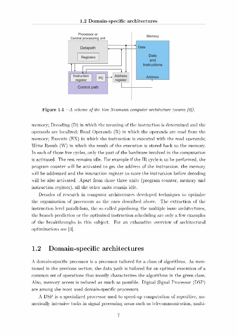
of a Von Neumann machine as shown in Figure 1.1 consists of:
- A memory for storing program and data. Harvard architectures contain two
parallel accessible memories for storing program and data separately.
- A control unit (also called control path) featuring a program counter that holds
the address of the next instruction to be executed.
- An arithmetic and logic unit (also called data path) in which instructions are
executed.
A program is coded as a set of instructions to be executed sequentially, instruction
after instruction. At each step of the program execution, the next instruction is
fetched from the memory at the address speci�ed in the program counter and decoded.
The required operands are then collected from the memory before the instruction is
executed. After execution, the result is written back into the memory. In this process,
the control path is in charge of setting all signals necessary to read from and write to
the memory, and to allow the data path to perform the right computation. The data
path is controlled by the control path, which interprets the instructions and sets the
control signals accordingly to execute the desired operation.
In general, the execution of an instruction on a Von Neumann computer can be
done in �ve cycles: Instruction Read (IR) in which an instruction is fetched from the
6
1.2 Domain-speci�c architectures
Figure 1.1 � A scheme of the Von Neumann computer architecture (source [2]).
memory; Decoding (D) in which the meaning of the instruction is determined and the
operands are localized; Read Operands (R) in which the operands are read from the
memory; Execute (EX) in which the instruction is executed with the read operands;
Write Result (W) in which the result of the execution is stored back to the memory.
In each of those �ve cycles, only the part of the hardware involved in the computation
is activated. The rest remains idle. For example if the IR cycle is to be performed, the
program counter will be activated to get the address of the instruction, the memory
will be addressed and the instruction register to store the instruction before decoding
will be also activated. Apart from those three units (program counter, memory and
instruction register), all the other units remain idle.
Decades of research in computer architectures developed techniques to optimize
the organization of processors as the ones described above. The extraction of the
instruction level parallelism, the so called pipelining, the multiple issue architectures,
the branch prediction or the optimized instruction scheduling are only a few examples
of the breakthroughs in this subject. For an exhaustive overview of architectural
optimizations see [3].
1.2 Domain-speci�c architectures
A domain-speci�c processor is a processor tailored for a class of algorithms. As men-
tioned in the previous section, the data path is tailored for an optimal execution of a
common set of operations that mostly characterizes the algorithms in the given class.
Also, memory access is reduced as much as possible. Digital Signal Processor (DSP)
are among the most used domain-speci�c processors.
A DSP is a specialized processor used to speed-up computation of repetitive, nu-
merically intensive tasks in signal processing areas such as telecommunication, multi-
7
Chapter 1. Introduction to recon�gurable computing
media, automobile, radar, sonar, seismic, image processing, etc. The most often cited
feature of DSPs is their ability to perform one or more multiply accumulate (MAC)
operations in single cycle. Usually, MAC operations have to be performed on a huge
set of data. In a MAC operation, data are �rst multiplied and then added to an
accumulated value. The normal Von Neumann computer would perform a MAC in
10 steps. The �rst instruction (multiply) would be fetched, then decoded, then the
operand would be read and multiply, the result would be stored back and the next
instruction (accumulate) would be read, the result stored in the previous step would
be read again and added to the accumulated value and the result would be stored
back. DSPs avoid those steps by using specialized hardware that directly performs the
addition after multiplication without having to access the memory.
Because many DSP algorithms involve performing repetitive computations, most
DSP processors provide special support for e�cient looping. Often a special loop or
repeat instruction is provided, which allows a loop implementation without expending
any instruction cycles for updating and testing the loop counter or branching back to
the top of the loop. DSPs are also customized for data with a given width according to
the application domain. For example if a DSP is to be used for image processing, then
pixels have to be processed. If the pixels are represented in Red Green Blue (RGB)
system where each colour is represented by a byte, then an image processing DSP will
not need more than 8 bit data path. Obviously, the image processing DSP cannot be
used again for applications requiring 32 bits computation.
This specialization of DSP's functions increases the performance of the processor
and improves device utilization, but reduces the execution e�ciency of an arbitrary
application.
1.3 Application-speci�c architectures
Although DSPs incorporate a degree of application-speci�c features such as MAC and
data width optimization, they still hide the Von Neumann approach and, therefore,
remain sequential machines. Their performance is limited. If a processor has to be
used for only one application, which is known and �xed in advance, then the processing
unit could be designed and optimized for that particular application. In this case, we
say that the hardware ��ts� itself to the application. This kind of approach is useful,
for instance, when a processor has to perform tasks de�ned by a standard, such as
encoding and decoding of an audio/video stream.
A processor designed for only one application is called an Application-Speci�c
Processor (ASIP). In an ASIP, the instruction cycles (IR, D, R, EX, W) are eliminated:
there is no fetch of instructions because the instruction set of the application is directly
implemented in hardware, or, in other words the algorithm to perform is hardwired in a
8

1.4 Programmable logic, FPGA
custom processor. Therefore a data stream works as input, the processor performs the
required computation and the results can be collected at the outputs of the processor.
ASIPs use a spatial approach to implement only one application. The gates build-
ing the �nal processor are con�gured so that they constitute all the functional units
needed for the computation of all parts of the application. This kind of computation
is called spatial computing [4]. Once again, an ASIP that is built to perform a given
computation cannot be used for other tasks other than those for which it has been
originally designed.
ASIPs are usually implemented as single chips called Application-Speci�c Integrated
Circuit, ASIC, or using devices housing programmable logic. This approach arose in
the late '80's with the widespread commercial availability of recon�gurable chips called
Field Programmable Gate Arrays, FPGAs.
1.4 Programmable logic, FPGA
The FPGA is a regularly tiled two-dimensional array of logic blocks. Each logic block
includes a Look-Up Table (LUT), a simple memory that can store an arbitrary n-input
boolean function. The logic blocks communicate through a programmable intercon-
nection network that includes both nearest neighbor as well as hierarchical and long
path wires. The periphery of the FPGA contains I/O blocks to interface between
the internal logic blocks and the I/O pins. This simple, homogeneous architecture has
evolved to become much more heterogeneous, including on-chip memory blocks as well
as DSP blocks such as multiply/multiply-accumulate units.
There are several sorts of FPGAs, including those that can be programmed only
once, but the application-speci�c architectures may require that the device can be
recon�gured on-the-�y during a run or between separate runs to obtains di�erent be-
haviours. Depending on the needs of the applications it is possible to use devices
basing their recon�guration on SRAM (faster) or FLASH (slower) but this is only a
technological detail. In both cases this means that the con�guration of the FPGA,
the object code de�ning the algorithm loaded onto the device, is stored in an on-chip
storage device. By loading di�erent con�gurations into this con�guration device, dif-
ferent algorithms can be executed. The con�guration determines the boolean function
computed by each logic block and the interconnection pattern between logic and I/O
blocks.
FPGA designers have developed a large variety of programmable logic structures
for FPGAs since their invention in the mid-1980's. For more than a decade, much of
the programmable logic used in FPGAs can be generalized as shown in Figure 1.2.
The basic logic element generally contains some form of programmable combinational
logic, a �ip-�op or latch, and some fast carry logic to reduce the area and delay costs
9
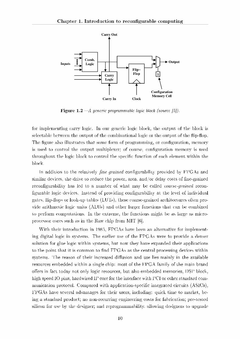
Chapter 1. Introduction to recon�gurable computing
Figure 1.2 � A generic programmable logic block (source [5]).
for implementing carry logic. In our generic logic block, the output of the block is
selectable between the output of the combinational logic or the output of the �ip-�op.
The �gure also illustrates that some form of programming, or con�guration, memory
is used to control the output multiplexer; of course, con�guration memory is used
throughout the logic block to control the speci�c function of each element within the
block.
In addition to the relatively �ne-grained con�gurability provided by FPGAs and
similar devices, the drive to reduce the power, area, and/or delay costs of �ne-grained
recon�gurability has led to a number of what may be called coarse-grained recon-
�gurable logic devices. Instead of providing con�gurability at the level of individual
gates, �ip-�ops or look-up tables (LUTs), these coarse-grained architectures often pro-
vide arithmetic logic units (ALUs) and other larger functions that can be combined
to perform computations. In the extreme, the functions might be as large as micro-
processor cores such as in the Raw chip from MIT [6].
With their introduction in 1985, FPGAs have been an alternative for implement-
ing digital logic in systems. The earlier use of the FPGAs were to provide a denser
solution for glue logic within systems, but now they have expanded their applications
to the point that it is common to �nd FPGAs as the central processing devices within
systems. The reason of their increased di�usion and use lies mainly in the available
resources embedded within a single chip: most of the FPGA family of the main brand
o�ers in fact today not only logic resources, but also embedded memories, DSP block,
high speed IO pins, hardwired IP core for the interface with PCI or other standard com-
munication protocol. Compared with application-speci�c integrated circuits (ASICs),
FPGAs have several advantages for their users, including: quick time to market, be-
ing a standard product; no non-recurring engineering costs for fabrication; pre-tested
silicon for use by the designer; and reprogrammability, allowing designers to upgrade
10
1.5 Recon�gurable Computing
or change logic through in-system programming. By recon�guring the device with a
new circuit, design errors can be �xed, new features can be added, or the function of
the hardware can be entirely retargeted to other applications. Of course, compared
with ASICs, FPGAs cost more per chip to perform a particular function so they are
not good for extremely high volumes. Also, an FPGA implementation of a function is
slower than the �xed-silicon options.
1.5 Recon�gurable Computing
From the discussion in sections 1.1 1.2 1.3, where we introduced three di�erent kinds of
processing units, we can identify two main means to characterize processors: �exibility
and performance.
The computers based on Von Neumann paradigm are very �exible because they
are in principle able to compute any kind of task: therefore we refer to them with
the terminology general purpose processors. Although there are many kind of opti-
mizing procedures and tricks their general purpose orientation has a cost in terms of
performance: for instance, the �ve steps (IR, D, R, EX, W) needed to perform one
instruction becomes a major drawback, in particular if the same instruction has to be
executed on huge sets of data; moreover their intrinsic sequential structure is useful
for the programmer because it is similar to the human thought process but is a natural
hindrance for a possible parallel computing approach for some applications. With this
architecture we have thus a high level of �exibility because the hardware structure is
�xed and, in many cases, is hidden to the programmer by the compiler that play the
role to ��t� the application in the hardware in order to be executed. We could use the
catchphrase: with general purpose processors the application must always �ts in the
hardware.
On the other side the application-speci�c architectures bring high performance
because they are optimized for a particular application. The instruction set required
for that application can then be built in a chip, but we pay a high cost in terms
of �exibility. In this case the important goals are the performance of the processor
and the hardware is shaped by the application. From this is possible we can invent
the opposite catchphrase: in presence of application-speci�c architectures the hardware
always �ts in the application.
Between these two extreme positions, general purpose processors and application-
speci�c processors, there is, architecturally speaking, an interesting space in which we
�nd di�erent types of processors. We can classify them depending on their performance
and their �exibility.
If we consider, after this analysis, the features of the FPGAs introduced brie�y in
section 1.4 we can easily see that they allow us to implement hardware architectures
11

Chapter 1. Introduction to recon�gurable computing
that merge the �exibility of a general purpose processor and the performance of an
application-speci�c processor with the comfort of the recon�gurability. In other words,
the boost that FPGA technology gives to researchers studying the architectures a
powerful tool to try to e�ciently �ll the space between general purpose and application-
speci�c processors. We consider therefore FPGAs as the way to build a recon�gurable
hardware or recon�gurable device or Recon�gurable Processing Unit, RPU, in analogy
with the Central Processing Unit, CPU. Following this, the study of computation using
recon�gurable devices is commonly called Recon�gurable Computing.
For a given application, at a given time, the spatial structure of the device will be
modi�ed such as to use the best computing approach to speed up that application.
If a new application has to be computed, the device structure will be modi�ed again
to match the new application. Contrary to the Von Neumann computers, which are
programmed by a set of instructions to be executed sequentially, the structure of
recon�gurable devices are changed by modifying all or part of the hardware at compile-
time or at run-time, usually by downloading a so called bitstream into the device. In
this sense we call con�guration or recon�guration the process of changing the structure
of a recon�gurable device respectively at star-up-time or at run-time.
Other than this di�erence of approach the major operative di�erences between
recon�gurable and processor-based computing are:
- The FPGA is con�gured into a customized hardware implementation of the ap-
plication. The hardware is usually data path driven, with minimal control �ow;
processor-based computing depends on a linear instruction stream including loops
and branches.
- The recon�gurable computer data path is usually pipelined so that all function
units are in use every clock cycle. The microprocessor has the potential for
multiple instructions per clock cycle, but the delivered parallelism depends on
the instruction mix of the speci�c program, and function units are often under-
utilized.
- The recon�gurable computer can access many memory words in each clock cycle,
and the memory addresses and access patterns can be optimized for the appli-
cation. The processor reads data through the data cache, and e�ciency of the
processor is determined by the degree to which data is available in the cache
when needed by an instruction. The programmer only indirectly controls the
cache-friendliness of the algorithm, as access to the data cache is hidden from the
instruction set architecture.
- The FPGA has in principle no constraints about the size of data words: the
words of the data path can have arbitrary length. Using the general purpose
architectures the length of the data words is �xed and the programmer has no
�ne control on it.
12
1.5 Recon�gurable Computing
To summarize, recon�gurable computing is concerned with decomposing applications
into spatially parallel, tiled, application-speci�c pipelines, whereas the traditional gen-
eral purpose processor interprets a linear sequence of instruction, with pipelining and
other forms of spatial parallelism hidden within the microarchitecture of the processor.
Progress in recon�guration has been amazing in the last two decades. This is
mostly due to the wide acceptance of the Field Programmable Gate Array (FPGAs)
that are now established as the most widely used recon�gurable devices.
1.5.1 Pervasiveness of RC
There are two main �elds in which the recon�gurable computing has been mostly
accepted, developed and used: embedded computing and scienti�c computing.
There are social reasons for that analyzed in [7]: people with expertise developing
embedded systems have hardware background and see in FPGAs a cheap solution to
develop custom systems with the possibility to �x with new �rmware releases their
projects so that the development and the update of an FPGA-based system is easier
and faster than with other components. Also this category of people with hardware
background is in many cases familiar with hardware description languages and with
hardware implementation techniques and can obtain impressive boost of performance
with a relative low prices and power consumption.
From scienti�c computing come problems often with very special requirements and
in many cases it is possible to implement their algorithms directly within an FPGA.
Depending on the project the FPGAs can be con�gured as the co-processor of a general
purpose processor or a main-custom processor. A limiting factor for to this kind of
project comes often from the absence of a speci�c hardware background of the people
involved: in some cases in fact the need to develop a design using hardware description
languages can require a long development period and a drastic change of the paradigm
of programming. Because of this some groups and companies develop and sell tools for
the translation of standard codes, like C, for instance, to various hardware description
language. These automatic tools of translation can speed up and make easier the
development process, but sometimes have big limitations on the code structures that
can be translated and the extraction of parallelism may not always be e�cient.
1.5.2 The Hartenstein's point of view
The most common architectural approach in computer science is the Von Neumann
paradigm and the most used processors are based on the general purpose architec-
tures. The recon�gurable computing approach requires a deep change of programming
paradigm in comparison with the Von Neumann: R. Hartenstein starting from 1990
gave a formalisation of it in [8, 9, 10]. Theoretically speaking, there is in the RC
13

Chapter 1. Introduction to recon�gurable computing
environment a di�erent view of the software and the hardware. In the Von Neumann
approach the hardware resources are �xed, only one source code is needed and the
compiler processing it generates an instruction-stream to be stored in the program
memory waiting the scheduled time to be executed.
The RC approach requires two di�erent type of source code, con�gware and �owware.
Con�gware is commonly written using some abstraction of an hardware description
language and is synthesised using a tool that translates the code describing the custom
architecture into logic gates, maps it on the FPGA resources and produces as output
a so called bitstream, a con�guration �le to properly set up the FPGA resources.
Flowware is code written with a high level programming language generating a stream
of data used as input for the custom architecture implemented within the FPGA. As
sometimes the platform housing the recon�gurable device is not a �standard� mother
board with �standard� communication protocols, the �owware implements also com-
munication interfaces and other features useful for the system. Recon�gurable systems
require moreover that con�guration/recon�guration of the logic is performed external
to the device: in some cases a PROM is used to set up the recon�gurable device on
boot, but it is useful to have the possibility to recon�gure the devices �on the �y�.
This require that �owware is able to perform this task too. Figure 1.3 summarize the
theoretical schemes of two approach: Von Neumann and recon�gurable computing.
Figure 1.3 � On the left the organization of Software Engineering in the classic Von
Neumann point of view; on the right a schema of the Con�gware Engineering theorized
by Hartenstein (adapted from [7]).
1.5.3 Man does not live by hardware only
On the theoretical side Hartenstein tries to formalize the principles of recon�gurable
computing. Following this idea and thanks to the increasing resources o�ered by the
FPGAs many people built therefore systems based on programmable logic and many of
14
1.6 Non exhaustive history of RC
these projects developed interfaces to connect general purpose architecture and FPGA
based systems [11, 12, 13, 14] trying to de�ne a standard interface in order to:
- access recon�gurable hardware resources without introducing undesirable depen-
dencies on hardware;
- avoid client code changes whenever the hardware is revised;
- leave the programmer free to know or ignore the hardware details of interfaces
or low level protocols;
- develop a set of libraries optimized for scienti�c computing and reprogrammable
logic based coprocessors [12].
All these e�orts are focused on solving a basic problem coming from recon�gurable
computing and formalized by Hartenstein: which is the way to e�ciently use the
huge degrees of freedom coming from the FPGA while maintaining programmability
accessible to a large part of the computer science community?
A �rst approach to solve it is to completely ignore the programmability and the gen-
eralization of the design in order to obtain the best performances from the logics: this
approach is commonly adopted by groups or projects developing e�cient application-
speci�c architectures that are not interested in developing a general purpose machine,
but only a performance oriented custom machine.
The second opposite approach comes from groups and projects studying systems
oriented to a large enough set of applications and in which the availability of as friendly
a programming environment as possible can justify a considerable loss of performance.
1.6 Non exhaustive history of RC
Like most technologies, recon�gurable computing systems are built on a variety of
existing technologies and techniques. It is always di�cult to pinpoint the exact mo-
ment a new area of technology comes into existence or even to pinpoint which is the
�rst system in a new class of machines. Popular scienti�c history often gives simple
accounts of individuals and projects that represent a turning point for a particular
technology, but in reality the story is usually more complicated.
The large number of exotic high-performance systems designed and built over a
very short time makes this area particularly di�cult to document, but there is also
a problem speci�c to them. Much of the work was done inside various government
agencies, particularly in the United States, and was never published. In these cases,
all that can be relied on is currently available records and publications.
15
Chapter 1. Introduction to recon�gurable computing
1.6.1 Common features
Recon�gurable systems are distinguished from other cellular multiprocessor systems.
Array processors, in particular Single Instruction Multiple Data Processors (SIMD),
are considered architecturally distinct from recon�gurable machines, in spite of many
similarities. This distinction arises primarily from the programming techniques. Ar-
ray processors tend to have either a shared or dedicated instruction sequencer and
take standard instruction-style programming code. Recon�gurable machines tend to
be programmed spatially, with di�erent physical regions of the device being con�g-
ured at di�erent times. This necessarily means that they will be slower to reprogram
than cellular multiprocessor systems but should be more �exible and achieve higher
performance for a given silicon area.
Although FPGA-based systems are very di�erent each others, it is possible to
extract some shared features concerning both architectures of systems housing recon-
�gurable devices and architecture of designs within the FPGAs.
The systems using FPGA are in many cases con�gured as master-slave systems: a
general purpose architecture works as master, runs the �owware and handles commu-
nications with the slave system with one or more recon�gurable devices. In general
slave systems are custom boards housing in addition to one or more FPGAs other
components like for instance external memory, communications devices, special I/O
devices etc. Although the structure of the system housing recon�gurable logics could
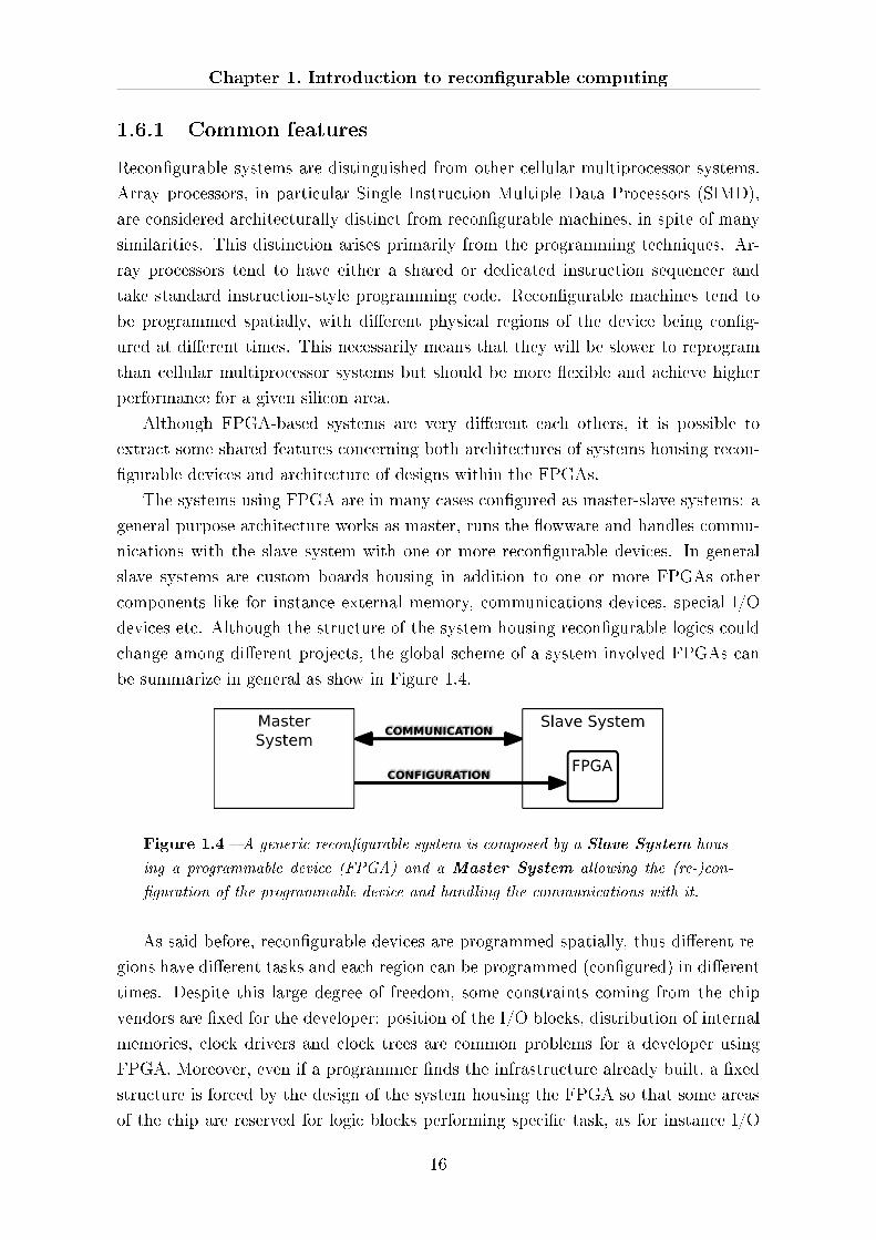
change among di�erent projects, the global scheme of a system involved FPGAs can
be summarize in general as show in Figure 1.4.
Figure 1.4 � A generic recon�gurable system is composed by a Slave System hous-
ing a programmable device (FPGA) and a Master System allowing the (re-)con-
�guration of the programmable device and handling the communications with it.
As said before, recon�gurable devices are programmed spatially, thus di�erent re-
gions have di�erent tasks and each region can be programmed (con�gured) in di�erent
times. Despite this large degree of freedom, some constraints coming from the chip
vendors are �xed for the developer: position of the I/O blocks, distribution of internal
memories, clock drivers and clock trees are common problems for a developer using
FPGA. Moreover, even if a programmer �nds the infrastructure already built, a �xed
structure is forced by the design of the system housing the FPGA so that some areas
of the chip are reserved for logic blocks performing speci�c task, as for instance I/O
16
1.6 Non exhaustive history of RC
interfaces or memory controllers. A common feature of all recon�gurable computing
projects is therefore the presence of some kind of spatial constraints.
1.6.2 Fix-plus machine (Estrin)
In 1959, Gerald Estrin, a computer scientist of the university of California at Los
Angeles, introduced the concept of recon�gurable computing. The following fragment
of an Estrin publication in 1960 [15] on the �x-plus machine, de�nes the concept of
recon�gurable computing paradigm.
�Pragmatic problem studies predicts gains in computation speeds in
a variety of computational tasks when executed on appropriate problem-
oriented con�gurations of the variable structure computer. The economic
feasibility of the system is based on utilization of essentially the same hard-
ware in a variety of special purpose structures. This capability is achieved
by programmed or physical restructuring of a part of the hardware.�
To implement this vision, Estrin designed a computing system, the �x-plus machine,
that like many recon�gurable computing systems available today, was composed of a
�xed architecture (a proto-general purpose processor) and a variable part consisting of
logic operators that could be manually changed in order to execute di�erent operations.
1.6.3 Rammig Machine
In the year 1977, Franz J. Rammig, a researcher at the university of Dortmund pro-
posed a concept for editing hardware [16]. The goal was:
�investigation of a system, which, with no manual or mechanical inter-
ference, permits the building, changing, processing and destruction of real
(not simulated) digital hardware.�
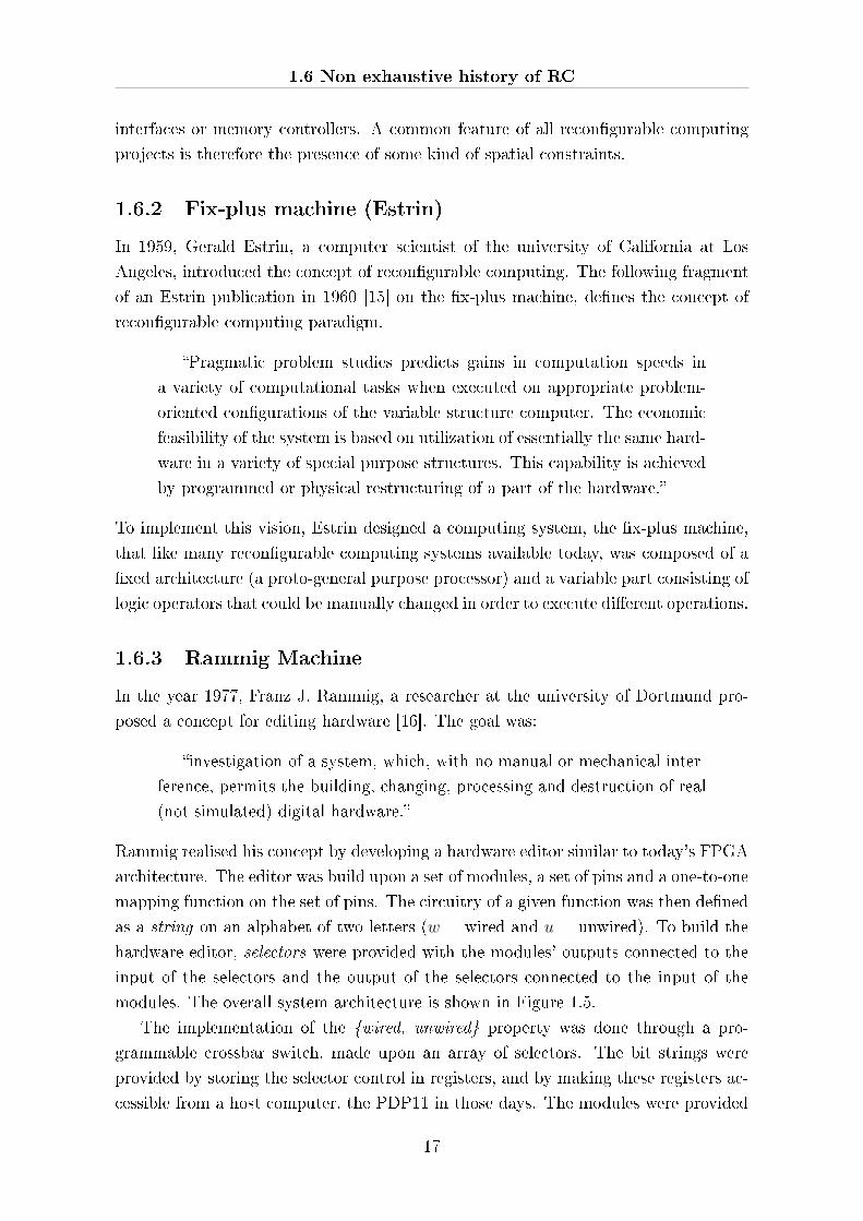
Rammig realised his concept by developing a hardware editor similar to today's FPGA
architecture. The editor was build upon a set of modules, a set of pins and a one-to-one
mapping function on the set of pins. The circuitry of a given function was then de�ned
as a string on an alphabet of two letters (w = wired and u = unwired). To build the
hardware editor, selectors were provided with the modules' outputs connected to the
input of the selectors and the output of the selectors connected to the input of the
modules. The overall system architecture is shown in Figure 1.5.
The implementation of the {wired, unwired} property was done through a pro-
grammable crossbar switch, made upon an array of selectors. The bit strings were
provided by storing the selector control in registers, and by making these registers ac-
cessible from a host computer, the PDP11 in those days. The modules were provided
17
Chapter 1. Introduction to recon�gurable computing
Figure 1.5 � Structure of the Rammig Machine (source [2]).
on a library board similar to that of Estrin's Fix-Plus. Each board could be selected
under software control. The mapping from module I/Os to pins was realized manually,
by a wiring of the provided library boards, i.e. �xed per library board.
1.6.4 Xputer (Hartenstein)
The Xputer's concept was presented in early 1980s by Reiner Hartenstein, a researcher
at the University of Kaiserslautern in Germany [8].
The goal was to have a very high degree of programmable parallelism in the hard-
ware, at the lowest possible level, to obtain performance not possible with the Von
Neumann computers. Instead of sequencing the instructions, the Xputer would se-
quence data, thus exploiting the regularity in the data dependencies of some class of
applications like image processing, where repetitive processing is performed on a large
amount of data. An Xputer consists of three main parts: the data sequencer, the data
memory and the recon�gurable ALU, rALU, that permits the run-time con�guration
of communication at levels below instruction set level. Within a loop, data to be pro-
cessed were accessed via a data structure called the scan window. Data manipulation
was done by the rALU that had access to many scan windows. The most essential
part of the data sequencer was the generic address generator, GAG, that was able to
produce address sequences corresponding to the data of up to three nested loops. An
rALU subnet that could be con�gured to perform all computations on the data of a
scan window was required for each level of a nested loop.
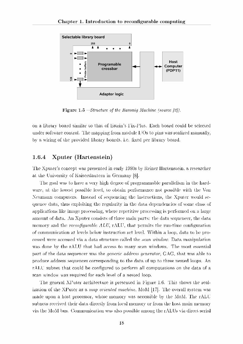
The general XPuter architecture is presented in Figure 1.6. This shows the real-
ization of the XPuter as a map oriented machine, MoM [17]. The overall system was
made upon a host processor, whose memory was accessible by the MoM. The rALU
subnets received their data directly from local memory or from the host main memory
via the MoM bus. Communication was also possible among the rALUs via direct serial
18
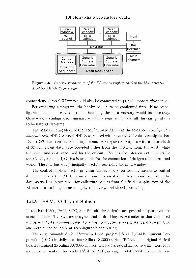
1.6 Non exhaustive history of RC
Figure 1.6 � General architecture of the XPuter as implemented in the Map oriented
Machine (MOM-3) prototype.
connections. Several XPuters could also be connected to provide more performance.
For executing a program, the hardware had to be con�gured �rst. If no recon-
�guration took place at run-time, then only the data memory would be necessary.
Otherwise, a con�guration memory would be required to hold all the con�gurations
to be used at run-time.
The basic building block of the recon�gurable ALU was the so-called recon�gurable
datapath unit, rDPU. Several rDPUs were used within an rALU for data manipulation.
Each rDPU had two registered inputs and two registered outputs with a data width
of 32 bit. Input data were provided either from the north or from the west, while
the south and east were used for the output. Besides the interconnection lines for
the rALUs, a global I/O-Bus is available for the connection of designs to the external
world. The I/O bus was principally used for accessing the scan windows.
The control implemented a program that is loaded on recon�guration to control
di�erent units of the rALU. Its instruction set consisted of instructions for loading the
data as well as instructions for collecting results from the �eld. Application of the
XPuters was in image processing, systolic array and signal processing.
1.6.5 PAM, VCC and Splash
In the late 1980s, PAM, VCC, and Splash, three signi�cant general-purpose systems
using multiple FPGAs, were designed and built. They were similar in that they used
multiple FPGAs, communicated to a host computer across a standard system bus,
and were aimed squarely at recon�gurable computing.
The Programmable Active Memories, PAM, project [18] at Digital Equipment Cor-
poration (DEC) initially used four Xilinx XC3000-series FPGAs. The original Perle-0
board contained 25 Xilinx XC3090 devices in a 5×5 array, attached to which were four
independent banks of fast static RAM (SRAM), arranged as 64K×64 bits, which were
19

Chapter 1. Introduction to recon�gurable computing
controlled by an additional two XC3090 FPGA devices. This wide and fast memory
provided the FPGA array with high bandwidth. The Perle-0 was quickly upgraded
to the more recent XC4000 series. As the size of the available XC4000-series devices
grew, the PAM family used a smaller array of FPGA devices, eventually settling on
2 × 2. Based at the DEC research lab, the PAM project ran for over a decade and
continued in spite of the acquisition of DEC by Compaq and then the later acquisition
of Compaq by Hewlett-Packard. PAM, in its various versions, plugged into the stan-
dard PCI bus in a PC or workstation and was marked by a relatively large number of
interesting applications as well as some groundbreaking work in software tools. It was
made available commercially and became a popular research platform.
The Virtual Computer from the Virtual Computer Corporation, VCC, [19] was per-
haps the �rst commercially available recon�gurable computing platform. Its original
version was an array of Xilinx XC4010 devices and I-Cube programmable intercon-
nect devices in a checkerboard pattern, with the I-Cube devices essentially serving as
a crossbar switch. The topology of the interconnection for these large FPGA arrays
was an important issue at this time: With a logic density of approximately 10K gates
and input/output (I/O) pins on the order of 200, a major concern was communica-
tion across FPGAs. The I-Cube devices were perceived as providing more �exibility,
although each switch had to be programmed, which increased the design complexity.
The �rst Virtual Computer used an 8× 8 array of alternating FPGA and I-Cube de-
vices. The exception was on the left and right sides of the array, which exclusively
used FPGAs, which consumed 40 Xilinx XC4010 FPGAs and 24 I-Cubes. Along the
left and right sides were 16 banks of independent 16 × 8K dual-ported SRAM, and
attached to the top row were 4 more banks of standard single-ported 256K × 32 bits
SRAM controlled by an additional 12 Xilinx XC4010 FPGAs. While this system was
large and relatively expensive, and had limited software support, VCC went on to o�er
several families of recon�gurable systems over the next decade and a half.
The Splash system [20, 21], from the Supercomputer Research Center (SRC) at
the Institute for Defense Analysis, was perhaps the largest and most heavily used
of these early systems. Splash was a linear array consisting of XC3000-series Xilinx
devices interfacing to a host system via a PCI bus. Multiple boards could be hosted in a
single system, and multiple systems could be connected together. Although the Splash
system was primarily built and used by the Department of Defense, a large amount
of information on it was made available. A Splash 2 [22] system quickly followed and
was made commercially available from Annapolis Microsystems. The Splash 2 board
consisted of two rows of eight Xilinx XC4010 devices, each with a small local memory.
These 16 FPGA/memory pairs were connected to a crossbar switch, with another
dedicated FPGA/memory pair used as a controller for the rest of the system. Much of
the work using Splash concentrated on defense applications such as cryptography and
20
1.6 Non exhaustive history of RC
pattern matching, but the associated tools e�ort was also notable, particularly some
of the earliest high-level language (HLL) to hardware description language (HDL)
translation software targeting recon�gurable machines. Speci�cally, the data parallel
C compiler and its debug tools and libraries provided recon�gurable systems with a
new level of software support.
PAM, VCC, and Splash represent the early large-scale recon�gurable computing
systems that emerged in the late 1980s. They each had a relatively long lifetime
and were upgraded with new FPGAs as denser versions became available. Also of
interest is the origin of each system. One was primarily a military e�ort (Splash),
another emerged from a corporate research lab (PAM), and the third was from a small
commercial company (Virtual Computer). It was this sort of widespread appeal that
was to characterize the rapid expansion of recon�gurable computing systems during
the 1990s.
1.6.6 Cray XD1
While the number of small recon�gurable coprocessing boards would continue to pro-
liferate as commercial FPGA devices became denser and cheaper, other new hardware
architectures were produced to address the needs of large-scale supercomputer users.
Unlike the earlier generation of boards and systems that sought to put as much recon-
�gurable logic as possible into a single uni�ed system, these machines took a di�erent
approach. In general, they were traditional multiprocessor systems, but each pro-
cessing node in them consisted of a very powerful commercial desktop microprocessor
combined with a large commercial FPGA device. Another factor that made these
systems unique is that they were all o�ered by mainstream commercial vendors.
The �rst recon�gurable supercomputing machine from Cray, the XD1 [23], is based
on a chassis of 12 processing nodes, with each node consisting of an AMD Opteron
processor. Up to 6 recon�gurable computing processing nodes, based on the Xilinx
Virtex-2 Pro devices, can also be con�gured in each chassis, and up to 12 chassis can be
combined in a single cabinet, with multiple cabinets making larger systems. Hundreds
of processing nodes can be easily con�gured with this approach.
1.6.7 RAMP (Bee2)
Around 2005 the choice of the computer hardware industry to focus production on
single-chip multiprocessors gave a boost to the idea of developing a system able to
simulate highly parallel architectures at hardware speeds. The Research Accelerator
for Multiple Processors, RAMP, is the open-source FPGA-based project that arose
from this idea [24, 25]: its main aim is to develop and share the hardware and software
necessary to create parallel architectures.
21

Chapter 1. Introduction to recon�gurable computing
The computational support of RAMP project is the system BEE2 [26] using Xilinx
Virtex-2 Pro FPGAs as primary and only processing elements. A peculiarity of this
system is the PowerPC 405 embedded on the FPGA that makes it possible to minimize
latency between microprocessor and recon�gurable logic while maximizing the data
throughput. Moreover the BEE2 system is an example of an FPGA-based system that
does not require explicitly a master system checking over the tasks of the recon�gurable
logic: each FPGA embeds in fact general purpose processors able to control itself.
Each BEE2 compute module consists of �ve Xilinx Virtex-2 Pro-70 FPGA chips,
each directly connected and logically organized into four compute FPGAs and one
control FPGA. The control FPGA has additional global interconnect interfaces and
control signals to the secondary system components, while the compute modules are
connected as a 2× 2 mesh.
The architecture of the BEE2 leaves some degrees of freedom and using the 4X
In�niband physical connections, the compute modules can be wired into many network
topologies, such as a 3D mesh. For applications requiring high-bisection-bandwidth
random communication among many compute modules, the BEE2 system is designed
to take advantage of commercial network switch technology, such as In�niband or
10G Ethernet. The compute module runs the Linux OS on the control FPGA with a
full IP network stack. Moreover each BEE2 system is equipped with high bandwidth
memories (DDR, DDR2) and other I/O interfaces.
As well as being a hardware architecture project, RAMP aims to support the
software community as it struggles to take advantage of the potential capabilities of
parallel microprocessors, by providing a malleable platform through which the software
community can collaborate with the hardware community.
1.6.8 FAST (DRC)
FPGA-Accelerated Simulation Technologies (FAST) [27], is a today's project devel-
oped by the University of Texas at Austin that attempts to speed up the simulation
of complex computer architectures. It gives a methodology to build extremely fast,
cycle-accurate full system simulators that run real applications on top of real operating
systems. Current state of the project allows one to boot unmodi�ed Windows XP ,
Linux 2.4 and Linux 2.6 and run unmodi�ed applications on top of those operating
systems at simulation speeds in the 1.2 MIPS range, between 100 and 1000 times faster
than Intel's and AMD's cycle-accurate simulators (e.g. which is fast enough to type
into Microsoft Word). I knew people of this project during my visit at the University
of Texas in summer 2008.
The hardware platform used to develop this project is a DRC development system
(DS2002). This machine contains a dual-socket motherboard, where one socket con-
tains an AMD Opteron 275 (2.2GHz) and the other socket contains a Xilinx Virtex-4
22

1.6 Non exhaustive history of RC
LX200 (4VLX200) FPGA. The Opteron communicates to the FPGA via HyperTrans-
port. The functional model runs on the Opteron and the timing model runs on the
FPGA. DRC provides libraries to read and write from the FPGA. Interesting feature
regarding the hardware platform is the fact that an FPGA uses a standard socket of
a general purpose processor and not custom interfaces.
1.6.9 High-Performance Recon�gurable Computing: Maxwell
and Janus
The high-performance computing �eld is traditionally dominated by clusters of general
purpose processors and a common approach of the scientists is to �nd a machine as fast
as possible to run a given code, if possible with no changes of it. This approach do not
require in principle an understanding of the architecture or the hardware features of
the machine running the code. On the other hand it is known that code optimization
with respect to architectural details improves the performance of applications.
Despite that there are studies about the viability of recon�gurable supercomputing
[28] and some projects with relevant results in this �eld.
The FPGA High Performance Computing Alliance (FHPCA) [29] was established
in 2004 and is dedicated to the use of Xilinx FPGAs to deliver new levels of compu-
tational performance for real-world industrial applications. Led by EPCC, the super-
computing centre at The University of Edinburgh, the FHPCA is funded by Scottish
Enterprise and builds on the skills of Nallatech Ltd, Alpha Data Ltd, Xilinx Develop-
ment Corporation, Algotronix and ISLI.
Maxwell [30, 31, 32] is a high-performance computer developed by the FHPCA
to demonstrate the feasibility of running computationally demanding applications on
an array of FPGAs. Not only can Maxwell demonstrate the numerical performance
achievable from recon�gurable computing, but it also serves as a testbed for tools and
techniques to port applications to such systems.
The unique architecture of Maxwell comprises 32 blades housed in an IBM Blade
Center. Each blade comprises one 2.8 GHz Xeon with 1 Gbyte memory and 2 Xilinx
Virtex-4 FPGAs each on a PCI-X subassembly developed by Alpha Data and Nallat-
ech. Each FPGA has either 512 Mbytes or 1 Gbyte of private memory. Whilst the
Xeon and FPGAs on a particular blade can communicate with each other over the
PCI bus (typical transfer bandwidths in excess of 600 Mbytes/s), the principal com-
munication infrastructure comprises a fast Ethernet network with a high-performance
switch linking the Xeons together and RocketIO linking the FPGAs. Each FPGA has
4 RocketIO links enabling the 64 FPGAs to be connected together in an 8×8 toroidal
mesh. The RocketIO has a bandwidth in excess of 2.5 Gbits/s per link.
Together these two principal interconnect subsystems enable the e�cient imple-
23

Chapter 1. Introduction to recon�gurable computing
mentation of parallel codes where there is a need both for intensive numerical process-
ing and for fast data communication between the cooperating processing elements.
The Parallel Toolkit developed by EPCC supports the decomposition of a numer-
ically intensive application into a set of cooperating modules running on the array of
Xeons in much the same way that many applications can be decomposed to run on a
cluster of PCs. Each module can then be further analysed to identify the numerical
�hot spots� which are then implemented on the FPGAs taking advantage of the fast
RocketIO linking the FPGAs for fast communications. The implementation of the
numerically intensive parts of the applications is accomplished using a combination of
tools such as DIME-C from Nallatech, Handel-C from Celoxica and VHDL available
from several vendors including Xilinx.
Janus is a project among universities of Italy and Spain with the main goal to
realize a FPGA-based parallel system optimized a speci�c class of statistical physics
simulations. Janus is composed of 256 Xilinx Virtex-4 FPGA organized in sets of 16
each connected via raw-ethernet Gigabit channel to a standard PC.
Both these projects give to the computer science community an e�cient proof that
recon�gurable computing can be used in order to obtain high performance machines
as with a general purpose environment, in the Maxwell case, as in a very special and
application speci�c case, in the Janus case. I discuss in depth details of Janus in the
next chapters.
24

Bibliography
[1] J. von Neumann, First Draft of a Report on the EDVAC,
http://www.zmms.tu-berlin.de/~modys/MRT1/2003-08-TheFirstDraft.pdf.
1.1
[2] C. Bobda, Introduction to Recon�gurable Computing: Architectures, Algorithms
and Applications, Springer (2007). 1.1, 1.5
[3] J. L. Hennessy, D. A. Patterson, Computer Architecture. A quantitative Approach
(Fourth Edition), published by Morgan Kaufmann (2007). 1.1
[4] A. DeHon, J. Wawrzynek, Recon�gurable Computing: What, Why, and Implica-
tions for Design Automation, Proceedings of the 36th ACM/IEEE conference on
Design automation, pp. 610 - 615 (1999). 1.3
[5] M. Gokhale, P. S. Graham, Recon�gurable Computing: Accelerating Computation
with Field-programmable Gate Arrays, Birkhäuser (2005). 1.2
[6] E. Waingold et al., Baring it all to Software: The Raw Machine, Computer, vol.
30, n. 9, pp. 86-93 (1997). 1.4
[7] R. Hartenstein, Why we need Recon�gurable Computing Education, Introduction,
opening session of the �rst International Workshop on Recon�gurable Computing
Education, Karlsruhe (2006). 1.5.1, 1.3
[8] R. Hartenstein, A. Hirschbiel, and M.Weber, Xputers - an open family of non Von
Neumann architectures, in 11th ITG/GI Conference on Architektur von Rechen-
systemen, VDE-Verlag (1990). 1.5.2, 1.6.4
[9] R. Hartenstein, Data-stream-based Computing: Models and Architectural Re-
sources, Informacije Midem (Ljubljana), vol. 33, part 4, pp. 228-235 (2003). 1.5.2
[10] R. Hartenstein, The von Neumann Syndrome, invited paper �Stamatis Vassiliadis
Memorial Symposium�, Delft, The Netherlands, (2007). 1.5.2
25

BIBLIOGRAPHY
[11] J. J. Koo et al., Evaluation of a high-level-language methodology for high-
performance recon�gurable computers Proceedings of the IEEE 18th Interna-
tional Conference on Application-Speci�c Systems, Architectures and Processors
(ASAP), pp. 30-35 (2007). 1.5.3
[12] S. Mohl, The Mitrion-C Programming Language Mitrionics Inc. (2005).
http://www.mitrionics.com/ 1.5.3
[13] G. Genest, R. Chamberlain, R. Bruce, Programming an FPGA-based Super Com-
puter Using a C-to-VHDL Compiler: DIME-C, Adaptive Hardware and Systems
AHS 2007, pp. 280-286 (2007). 1.5.3
[14] P. Waldeck, N. Bergmann, Dynamic hardware-software partitioning on recon-
�gurable system-on-chip, Proceedings of 3rd IEEE International Workshop on
System-on-Chip for Real-Time Applications, pp. 102-105 (2003). 1.5.3
[15] G. Estrin and R. Turn, Automatic assignment of computations in a variable struc-
ture computer system, IEEE Transactions on Electronic Computers, vol. 12, n. 5,
pp. 755-773 (1963). 1.6.2
[16] F. J. Rammig, A concept for the editing of hardware resulting in an automatic
hardware-editor, in Proceedings of 14th Design Automation Conference, New Or-
leans, pp. 187-193 (1977). 1.6.3
[17] R. Hartenstein et al., MOM-map-oriented machine-a partly custom-designed ar-
chitecture compared to standard hardware, in Proceedings of CompEuro '89., pp.
7-9 (1989). 1.6.4
[18] P. Bertin, D. Roncin, and J. Vuillemin, Introduction to programmable active mem-
ories, in Systolic Array Processors, Prentice Hall, pp. 301-309 (1989). 1.6.5
[19] S. Casselman, Virtual computing and the Virtual Computer, Proceedings of IEEE
Workshop on FPGAs for Custom Computing Machines, pp. 43-48 (1993). 1.6.5
[20] M. Gokhale et al., Splash: A recon�gurable linear logic array, International Con-
ference on Parallel Processing, pp. 526-532 (1990). 1.6.5
[21] M. Gokhale et al., Building and Using a Highly Parallel Programmable Logic
Array, Computer, Volume 24, Issue 1, pp. 81-89 (1991). 1.6.5
[22] D. A. Buel, et al., Splash 2 FPGAs in a Custom Computing Machine, IEEE
Computer Society Press, Los Alamitos, California (1996). 1.6.5
[23] J. S. Vetter et al., Early Evaluation of the Cray XD1, Proceedings of 20th Inter-
national Parallel and Distributed Processing Symposium (2006). 1.6.6
26
BIBLIOGRAPHY
[24] J. Wawrzynek, D. Patterson et al., RAMP: Research Accelerator for Multiple
Processors IEEE Micro, vol. 27, n. 2, pp. 46-57 (2005). 1.6.7
[25] A. Krasnov et al., RAMP Blue: A Message-Passing Manycore System in FPGAs,
International Conference on Field Programmable Logic and Applications, pp. 54-
61 (2007). 1.6.7
[26] C. Chang, J. Wawrzynek, R. W. Brodersen, BEE2: A High-End Recon�gurable
Computing System, IEEE Design and Test of Computers, vol. 22, n. 2, pp. 114-125
(2005). 1.6.7
[27] D. Chiou et al., FPGA-Accelerated Simulation Technologies (FAST): Fast, Full-
System, Cycle-Accurate Simulators, Proceedings of the 40th Annual IEEE/ACM
International Symposium on Microarchitecture, pp. 249-261 (2007).
http://users.ece.utexas.edu/~derek/FAST.html 1.6.8
[28] S. Craven, P. Athanas, Examining the Viability of FPGA Supercomputing,
EURASIP Journal on Embedded Systems, vol. 2007, n. 93652 (2007). 1.6.9
[29] http://www.fhpca.org 1.6.9
[30] R. Baxter et al, High-Performance Recon�gurable Computing the View from Ed-
inburgh, Proceedings AHS2007 Conference Second NASA/ESA Conference on
Adaptive Hardware andSystems, Edinburgh (2007).
http://www.fhpca.org/download/HPRC.pdf 1.6.9
[31] R. Baxter et al, The FPGA High-Performance Computing Alliance Parallel
Toolkit, Proceedings AHS2007 Conference Second NASA/ESA Conference on
Adaptive Hardware andSystems, Edinburgh (2007).
http://www.fhpca.org/download/PTK.pdf 1.6.9
[32] R. Baxter et al., Maxwell a 64 FPGA Supercomputer, Proceedings AHS2007 Con-
ference Second NASA/ESA Conference on Adaptive Hardware andSystems, Ed-
inburgh (2007).
http://www.fhpca.org/download/RSSI07-Maxwell.pdf 1.6.9
27

They tried to take me to a doctor, but its too late for me.
Then they took me to a preacher that they saw on their tv
who said that for a small donation my lost soul would be saved
I said I don't think so preacher, I'll come back another day.
Bon Jovi
2Monte Carlo methods for statistical physics
This chapter is about the use of computers to solve problems in statistical physics.
In particular, it is about Monte Carlo methods, which form the largest and most
important class of numerical methods used for solving statistical physics problems.
In the opening section, I look �rst at what we mean by statistical physics, giving
a brief overview of the discipline called statistical mechanics with special care to two
examples: the Edward-Anderson model and the Potts model applied to the problem of
a random graph coloring. These two models are in fact implemented with impressive
boost of performances on the Janus supercomputer. The material presented here is
largely inspired by references [1, 2] and [3].
In section 2.2 I introduce Monte Carlo methods in general and I explain how they
can be used to explore statistical mechanics problems.
The last section will be dedicated to the computational features of Monte Carlo
implementation on a standard architecture. A special care will be given to the problem
of random numbers generation.
2.1 Statistical Physics
Statistical mechanics is primarily concerned with the calculation of properties of con-
densed matter systems. The crucial di�culty associated with these systems is that
they are composed of very many parts, typically atoms or molecules. These parts
are usually all the same or of a small number of di�erent types and they often obey
29
Chapter 2. Monte Carlo methods for statistical physics
quite simple equations of motion so that the behaviour of the entire system can be
expressed mathematically in a straightforward manner. However the complexity of
the problem makes it impossible to solve the mathematics exactly. A standard ex-
ample is that of a volume of gas in a container. One litre of, for instance, oxygen at
standard temperature and pressure consists of about 3 × 10²² oxygen molecules, all
moving around and colliding with one another and the walls of the container. One
litre of air under the same conditions contains the same number of molecules, but
they are now a mixture of oxygen, nitrogen, carbon dioxide. The atmosphere of the
Earth contains 4 × 1024 litres of air, or about 1 × 1044 molecules, all moving around
and colliding with each other and with the environment. It is not feasible to solve
Hamilton's equations for these systems because there are too many equations, and yet
when we look at the macroscopic properties of the gas, they are very well-behaved and
predictable. Clearly, there is something special about the behaviour of the solutions
of these many equations that �averages out� to give us a predictable behaviour for
the entire system. For example, the pressure and temperature of the gas obey quite
simple laws although both are measures of rather gross average properties of the gas.
Statistical mechanics attempts to avoid the problem of solving the equations of motion
and to compute these gross properties of large systems by treating them in a proba-
bilistic fashion. Instead of looking for exact solutions, we deal with the probabilities of
the system being in one state or another hence the name statistical mechanics. Such
probabilistic statements are extremely useful, because we usually �nd that for large
systems the range of behaviours of the system that have a non negligible probability
to occur is very small; all the reasonably probable behaviours fall into a narrow range,
allowing us to state with extremely high con�dence that the real system will display
behaviour within that range.
The typical paradigm for the systems we will be studying in this section is one of
a system governed by a Hamiltonian function H which gives us the total energy of the
system in any particular state. We only consider systems that have discrete sets of
states each with its own energy, ranging from the lowest, or ground state energy E0
upwards, E1, E2, E3, ... , possibly without limit.
If the system were in insulation energy would be conserved, which means that the
system would stay in the same energy state all the time (or if there were a number
of degenerate states with the same energy, maybe it would make transitions between
those) However there is another component to our paradigm, and that is the thermal
reservoir. This is an external system which acts as a source and sink of heat, constantly
exchanging energy with our Hamiltonian system in such a way as always to push
the temperature of the system, de�ned as in classical thermodynamics, towards the
temperature of the reservoir. In e�ect the reservoir is a weak perturbation on the
Hamiltonian, which we ignore in our calculation of the energy levels of our system,
30
2.1 Statistical Physics
but which pushes the system frequently from one energy level to another. We can
incorporate the e�ects of the reservoir in our calculations by giving the system a
dynamics, a rule whereby the system changes periodically from one state to another.
The exact nature of the dynamics is dictated by the form of the perturbation that
the reservoir produces in the Hamiltonian. However, there are a number of general
conclusions that we can reach without specifying the exact form of the dynamics, and
we will examine these �rst.
Suppose our system is in a state µ. Let us de�ne R(µ→ ν)dt to be the probability
that it is in state ν a time dt later. R(µ→ ν) is the transition rate for the transition
from µ to ν. The transition rate is normally assumed to be time independent and we
will make that assumption here. We can de�ne a transition rate like this for every
possible state ν that the system can reach. These transition rates are usually all we
know about the dynamics, which means that even if we know the state µ that the
system starts o� in, we need only wait a short interval of time and it could be in any
one of a very large number of other possible states. This is where our probabilistic
treatment of the problem comes in. We de�ne a set of weights wµ(t) which represent
the probability that the system will be in state µ at time t. Statistical mechanics deals
with these weights, and they represent our entire knowledge about the state of the
system. We can write a master equation for the evolution of wµ(t) in terms of the
rates R(µ→ ν) thus:
dwµdt
=∑ν
[wν(t)R(ν → µ)− wµ(t)R(µ→ ν)] (2.1.1)
The �rst term on the right-hand side of this equation represents the rate at which
the system is undergoing transitions into state µ the second term is the rate at which
it is undergoing transitions out of µ into other states. The probabilities wµ(t) must
also obey the sum rule
∑µ
wµ(t) = 1 (2.1.2)
for all t, since the system must always be in some state. The solution of Equation
2.1.1, subject to the constraint 2.1.2, tells us how the weights wµ vary over time.
We must now consider how the weights wµ relate to the macroscopic properties of
the system which we study. If we are interested in some quantity Q, which takes the
value Qµ in state µ, then we can de�ne the expectation of Q at time t for our system
as
〈Q〉 =∑µ
Qµwµ(t). (2.1.3)
31

Chapter 2. Monte Carlo methods for statistical physics
Clearly this quantity contains important information about the real value of Q that
we might expect to measure in an experiment. For example, if our system is de�nitely
in one state τ then 〈Q〉 will take the corresponding value Qτ . And if the system is
equally likely to be in any of three states, and has zero probability of being in any other
state, then 〈Q〉 is equal to the mean of the values of Q in those three states. However,
the precise relation of 〈Q〉 to the observed value of Q must be considered more closely.
There are two ways to look at it. The �rst is to imagine having a large number of
copies of our system all interacting with their own thermal reservoirs and making
transitions between one state and another all the time. 〈Q〉 is then a good estimate of
the number we would get if we were to measure the instantaneous value of the quantity
Q in each of these systems and then take the mean of all of them. This is a conceptually
sound approach to de�ning the expectation of a quantity. However this de�nition is not
closely related to what happens in a real experiment. In a real experiment we normally
only have one system and we make all our measurements of Q on that system, though
we probably don't just make a single instantaneous measurement, but rather integrate
our results over some period of time. There is another way of looking at the expectation
value which is similar to this experimental picture. This is to envisage the expectation
as a time average of the quantity Q. Imagine recording the value of Q every second
for a thousand seconds and taking the average of those one thousand values. This will
correspond roughly to the quantity calculated in Equation 2.1.3 as long as the system
passes through a representative selection of the states in the probability distribution
wµ, in those thousand seconds. Obviously we will get an increasingly accurate �t
between our experimental average and the expectation 〈Q〉 as we average over longerand longer time intervals. Conceptually there is a weakness in this approach as we
do not have a rigorous de�nition of what we mean by a �representative selection of
the states�. There is no guarantee that the system will pass through anything like a
representative sample of the states of the system in the time during which we observe
it. It could easily be that the system only moves from one state to another on longer
time scales and so it remains in the same state for all of our measurements. Or maybe
it changes state very rapidly, but because of the nature of the dynamics spends long
periods of time in small portions of the state space. This can happen for example if
the transition rates R(µ→ ν) are only large for states of the system that di�er in very
small ways, so that the only way to make a large change in the state of the system is
to go through very many small steps. This is a very common problem in a lot of the
systems. Another potential problem with the time average interpretation of 2.1.3 is
that the weights wµ(t), which are functions of time, may change considerably over the
course of our measurements, making the expression invalid. For equilibrium systems
the weights are by de�nition not time-varying, so this problem does not arise. Despite
these problems however, this interpretation of the expectation value of a quantity is
32
2.1 Statistical Physics
the most widely used and most experimentally relevant interpretation. The calculation
of expectation values is one of the fundamental goals of statistical mechanics, and of
Monte Carlo simulation in statistical physics.
2.1.1 Spin Glass
Spin glass materials are diluted magnetic materials with long range interactions with
oscillating signs, that can be accurately described by statistical mechanical models
where the quenched couplings have zero average and are randomly distributed: they
have played a crucial role in the development of a new paradigm [4]. Recently the
replica symmetry breaking (RSB) solution of the mean �eld theory has been proven to
be correct [5, 6], but many of its implications, already at the mean �eld level, have yet
to be unveiled, and its relations with realistic models of three dimensional materials
are not yet clear.
This paradigm is of remarkable interest for at least four di�erent reasons. First
the theoretical structure that emerges from the RSB is very complex and very new,
di�erent from the most part of typical features of physical systems. Second it sheds at
least some lights on materials in the universality class of spin glasses (that is far larger
of the one including magnetic samples). Third it will hopefully allow us to advance in
our understanding of structural glasses [7], where in the absence of quenched disorder
it is the intrinsic complexity of the Hamiltonian which dynamically induces frustration.
Fourth it allows us to analyze (and sometimes to brilliantly solve) a large number of
non physics problems: optimization, �nancial markets and complex networks can be
studied thanks to the tools and algorithms created for studying spin glasses.
The typical Hamiltonian is
H = −∑
Jijsisj , (2.1.4)
where the s variables are the basic degrees of freedom of the model and can take the
values ±1 (models where the variables are de�ned on a µ dimensional spheres are for
example also of interest), i and j are sites of a D dimensional lattice (typically simple
cubic) and the couplings J are quenched random variables de�ned on the links of the
lattice (among �rst neighboring sites in D dimensions or among all couples of sites for
the mean �eld theory) that can take both signs and have a zero average (they can be
for example ±1 with equal probability or normal variables).
We consider a spin glass system as a collection of spins (i.e. magnetic moments)
that presents a frozen disordered low temperature state, instead of the uniform or
periodic pattern usually found in magnetic systems. In order to produce such a state,
two key ingredients turn out to be necessary: frustration (i.e. competition among the
di�erent interactions between magnetic moments, so that they cannot be all satis�ed
simultaneously) and disorder in the form of quenched randomness (i.e. each interaction
33
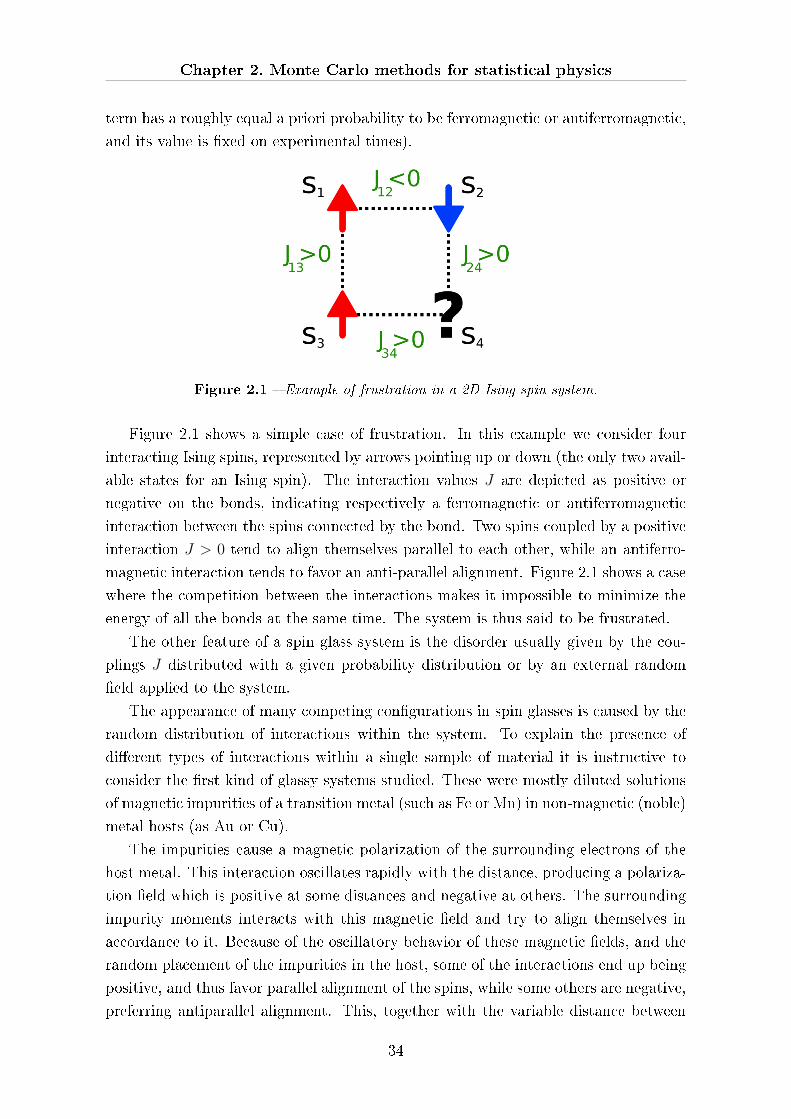
Chapter 2. Monte Carlo methods for statistical physics
term has a roughly equal a priori probability to be ferromagnetic or antiferromagnetic,
and its value is �xed on experimental times).
Figure 2.1 � Example of frustration in a 2D Ising spin system.
Figure 2.1 shows a simple case of frustration. In this example we consider four
interacting Ising spins, represented by arrows pointing up or down (the only two avail-
able states for an Ising spin). The interaction values J are depicted as positive or
negative on the bonds, indicating respectively a ferromagnetic or antiferromagnetic
interaction between the spins connected by the bond. Two spins coupled by a positive
interaction J > 0 tend to align themselves parallel to each other, while an antiferro-
magnetic interaction tends to favor an anti-parallel alignment. Figure 2.1 shows a case
where the competition between the interactions makes it impossible to minimize the
energy of all the bonds at the same time. The system is thus said to be frustrated.
The other feature of a spin glass system is the disorder usually given by the cou-
plings J distributed with a given probability distribution or by an external random
�eld applied to the system.
The appearance of many competing con�gurations in spin glasses is caused by the
random distribution of interactions within the system. To explain the presence of
di�erent types of interactions within a single sample of material it is instructive to
consider the �rst kind of glassy systems studied. These were mostly diluted solutions
of magnetic impurities of a transition metal (such as Fe or Mn) in non-magnetic (noble)
metal hosts (as Au or Cu).
The impurities cause a magnetic polarization of the surrounding electrons of the
host metal. This interaction oscillates rapidly with the distance, producing a polariza-
tion �eld which is positive at some distances and negative at others. The surrounding
impurity moments interacts with this magnetic �eld and try to align themselves in
accordance to it. Because of the oscillatory behavior of these magnetic �elds, and the
random placement of the impurities in the host, some of the interactions end up being
positive, and thus favor parallel alignment of the spins, while some others are negative,
preferring antiparallel alignment. This, together with the variable distance between
34

2.1 Statistical Physics
impurities, results in a set of random, competing interactions.
2.1.2 Edward-Anderson model
This model was introduced by Edwards and Anderson in 1975. One of their most
important contributions consisted in being able to capture the very essence of the spin
glass phenomenon within a model apparently simple and beautifully minimal, and
yet o�ering a rich and complex phenomenology at the same time. This boosted the
theoretical work on the �eld, and paved the way for other simpli�ed models.
Figure 2.2 � Three dimensional cubic lattice. The magnetic moments, placed in all
lattice nodes, are Ising-like variables ±1 (i.e. up/down). In this case the interactions
between nearest neighbors (represented by continuous lines in the �gure) are taken from
a bimodal distribution, and can be either ferromagnetic (+) or antiferromagnetic (-)
(source [3]).
The Edwards-Anderson (EA) model is de�ned on a regular three dimensional cubic
lattice of size L, usually with periodic boundary conditions and with the spins Si lying
on the V = L3 sites i of the lattice (see Figure 2.2 ). Its Hamiltonian can be written
as
H = −∑〈i,j〉
Jijsisj , (2.1.5)
where 〈i, j〉 means that the sum is performed only over nearest neighbors, and the
interactions Jij are independent random variables. In general the precise form of the
distribution of the Jij is not very important, as far as it produces a disordered and
frustrated system, but typically one uses either a Gaussian distribution with mean J0
and standard deviation unity
P (Jij) =1√2πe−(Jij−J0)/2, (2.1.6)
35
Chapter 2. Monte Carlo methods for statistical physics
or a double delta distribution with zero mean
P (Jij) =1
2[δ(Jij − 1) + δ(Jij + 1)]. (2.1.7)
The spins si are classicalm-component vectors (here indicated with bold font). The
simplest version of the model considers the case with m = 1, the so-called Ising model,
but a lot of theoretical work has been done also with m = 2 (the XY model), m = 3
(the Heisenberg model) and even higher number of components. In the literature the
name Edwards-Anderson models is often used to indicate exclusively the version with
Ising-like (i.e. m = 1 and si = ±1) spins and nearest neighbors interactions. We will
usually refer to this model in the following sections, and will therefore use the scalar
notation si for the spin, instead of the vectorial si .
The EA model can be easily generalized to accommodate the contribution of an
external magnetic �eld h whose value can vary randomly from one point of the lattice
to another. It is indicated as hi (as a function of the site i) and the resulting generalized
Hamiltonian function is
H = −∑〈i,j〉
Jijsisj −∑i
hisi . (2.1.8)
The apparent simplicity of the EA model, yet showing such a rich behavior, moti-
vated a lot of researchers to develop alternative models to help advancements in spin
glass theory. Many variations and di�erent models have been introduced and studied
during the last decades, such as, for instance the Sherrington-Kirkpatrick (SK) model
[8, 4] in which each spin interacts with all others spins and not only with the nearest
neighbours.
2.1.3 The Potts model and random graph coloring
The standard p-state Potts glass model is de�ned by the Hamiltonian
H = −∑〈i,j〉
Jijsisj , (2.1.9)
where si ∈ {1, 2, ..., p}, and the couplings {J} are random values. As it appears,
an energy term −Jij is gained (or lost, depending on the sign of Jij ) if the two spins
are in the same state, while the contribution is zero for spin in di�erent states. The
spins lie on a three-dimensional lattice of linear size L.
It is common to rede�ne the Hamiltonian by making use of the simplex represen-
tation of the Potts spins [9] which maps the p states of the (scalar) spins si to vectors
si in a (p − 1)-dimensional space, pointing to the corners of a p − simplex2 . The p
vectors de�ned in this way satisfy the relation
sasb =pδab − 1
p− 1(2.1.10)
36
2.1 Statistical Physics
where a and b are scalar Potts states (thus a, b ∈ {1, 2, ..., p}).This choice leads to the modi�ed Hamiltonian
H = −∑〈i,j〉
J ′ijsisj , (2.1.11)
which is analogous to a vector spin model in (p− 1) dimensions, with the substantial
di�erence that the spin vectors can take only a discrete set of values. Furthermore,
except for the case with p = 2 (which is just the EA-Ising model), given a spin si its
inverse −si is not allowed.The simplex Hamiltonian is commonly used to study this class of models, since it
helps to de�ne the relevant observables and order parameters. The couplings Jij are
usually drawn from a Gaussian or a bimodal distribution, as for the EA model. It is
not clear whether the choice on the distribution leading the disorder does a�ect or not
the system behavior. It has been suggested [10] that the Gaussian and the bimodal
Potts glass might belong to di�erent universality classes, though numerical simulations
like those in [11] and [12] show incompatible results and a quite di�erent behavior.
The Potts model is relevant not only because it represents a generalization of EA
model but also because it is an alternative formulation of the coloring problem on a
random graphs. A random graph is obtained by starting with a set of n vertices and
adding edges between them with a given di�erent probability distributions. The Erdös-
Rényi model for the random graphs is a common model [13, 14] in which the graph
is denoted as G(V,E), a set of V vertices and E edges occurring with a probability
p. For any graph G = (V,E), the set E of edges of G may be understood as a binary
relation on V . This is the adjacency relation of G, in which vertices a and b are related
precisely if {a, b} ∈ E, so ab is an edge of G. Conversely, every symmetric relation R
on V gives rise to (and is the edge set of) a graph on V (see [15] for an exhaustive
review). If we consider a set of p colors and we assume that each vertex has one of
these colors, we can de�ne a con�ict in a colors con�guration when two node connected
by an edge (adjacent vertices) have the same color. The coloring problem consists of
�nding a color con�guration of V , the set of the vertices, so that each vertex has a
color and each edge has no con�icts. The reader can surely guess that also in the
coloring problem there may exist the sort of frustration close to the de�nition given
in Figure 2.1.
Analytic work [16] and numerical studies in [17] [18] prove that there exist inter-
esting relations between the Potts model studying glassy systems in physics and the
Erdös-Rényi model solving the coloring problem on random graphs. The basic idea
of this equivalence is given in Figure 2.3: the p states of a spin in a Potts model
correspond to p colors of a vertex in a random graph model. Therefore it is possible
to de�ne a Hamiltonian function as in 2.1.9 for a random graph too and to study a
random graph with techniques similar to the ones used for spin systems. The only
37

Chapter 2. Monte Carlo methods for statistical physics
Figure 2.3 � Analogy between random graph coloring problem and Potts model.
di�erence lies in the geometry of the lattice: in a spin system the lattice is regular and
each spin has a �xed number of neighbours with which it interacts (in a 3D lattice the
neighbours are 6); by contrast in a random graph the number of adjacent nodes of a
given node is given by a distribution of probability and is not �xed.
From the perspective of the scientist studying the random graph problem, this
feature related to the topology of the system is not constrictive and approaching a
random graph with spin model techniques is useful and interesting because it allows
one to discover and prove important properties of random graphs. On the other hand,
if we look at the topology of the system with the eyes of the computer scientist, we
note immediately that while in spin system the regular lattice can be very e�ciently
mapped into a two-dimensional structure (i.e. a memory in a computer), an irregular
structure of information as given by the random graph problem represents a non trivial
challenge if we think about the manner to e�ciently store and access data in a memory.
I studied this kind of problems during the prototyping phase of the Janus system
[19] as described in details in Section 3.5.
2.2 Monte Carlo in general
2.2.1 Markov processes
Markov processes are stochastic processes whose futures are conditionally indepen-
dent of their pasts given their present values. More formally, a stochastic process
{Xt, t ∈ T }, with T ⊆ R, is called a Markov process if, for every s > 0 and t,
(Xt+s|Xu, u 6 t) ∼ (Xt+s|Xt) (2.2.1)
In other words, the conditional distribution of the future variable Xt+s, given the
entire past of the process {Xu, u 6 t} , is the same as the conditional distribution of
Xt+s given only the present Xt. That is, in order to predict future states, we only
need to know the present one. Property (2.2.1) is called the Markov property.
38

2.2 Monte Carlo in general
Depending on the index set T and state space E (the set of all values the {Xt}can take), Markov processes come in many di�erent forms. A Markov process with a
discrete index set is called a Markov chain. A Markov process with a discrete state
space and a continuous index set (such as R or R+) is called a Markov jump process.
2.2.2 Markov chains
Consider a Markov chain X = {Xt, t ∈ N} with a discrete (that is, countable) state
space E . In this case the Markov property (2.2.1) is:
P (Xt+1 = xt+1 |X0 = x0, ..., Xt = xt) = P (Xt+1 = xt+1 |Xt = xt) (2.2.2)
for all x0, ..., xt+1 ∈ E and t ∈ N. We restrict ourselves to Markov chains for which
the conditional probability
P (Xt+1 = j |Xt = i), i, j ∈ E (2.2.3)
is independent of the time t. Such chains are called time-homogeneous. The probabil-
ities in (2.2.3) are called the (one-step) transition probabilities of X. The distribution
of X0 is called the initial distribution of the Markov chain. The one-step transition
probabilities and the initial distribution completely specify the distribution of X. If
we consider the product rule of probability for any sequence of events A1, A2, . . . , An,
P (A1 · · ·An) = P (A1)P (A2|A1)P (A3|A1A2) · · ·P (An|A1 · · ·An−1) , (2.2.4)
using the abbreviation A1A2 · · ·Ak ≡ A1∩A2∩· · ·∩Ak and the Markov property 2.2.1
we obtain
P (X0 = x0, . . . , Xt = xt) =
= P (X0 = x0)P (X1 = x1|X0 = x0) · · ·P (Xt = xt|X0 = x0 . . . Xt−1 = xt−1)
= P (X0 = x0)P (X1 = x1|X0 = x0) · · ·P (Xt = xt|Xt−1 = xt−1)
(2.2.5)
Since E is countable, we can arrange the one-step transition probabilities in an array.
This array is called the (one-step) transition matrix of X denoted by T . For example,
when E = {0, 1, 2, . . . } the transition matrix T has the form
T =
p00 p01 p02 · · ·p10 p11 p12 · · ·p20 p21 p22 · · ·...
......
. . .
(2.2.6)
Note that the elements in every row are positive and sum up to unity. Another con-
venient way to describe a Markov chain X is through its transition graph. Figure 2.4
39

Chapter 2. Monte Carlo methods for statistical physics
Figure 2.4 � A transition graph: each numbered circle represents a state and each
directional link between states has a probability w that is the probability that the system
passes from a given state to another (following the arrow direction). The transition
graph A can be split in 2 independent Markov chains, B and C. Moreover the chain D
can be reduced to the chain E because no transitions are possible from a state of E to
a state of D. Markov chain E is instead irreducible (adapted from [20]).
shows a graph in which each node is a state and the edges link vertices with non-zero
transition probability. For instance, if we are in state 2 at a given time t, the con-
�guration at time t + 1 could be state 4, with probability w24 = 13, or state 7, with
probability w27 = 115, or to stay in state 2, with probability w22 = 3
5. From properties
of the probability we assume that ∑j
wij = 1 (2.2.7)
and the probability to be in a given state i at a given time t+ 1 is
pi(t+ 1) =∑j
pj(t)wji, (2.2.8)
where pj(t) is the probability to be in the state, j, at the previous time, t; wji represents
the probability to evolve from state j to state i in the last time step. From (2.2.7) and
(2.2.8) we obtain again (2.2.5) in the form
pi(t+ 1)− pi(t) =∑j
pj(t)wji −∑j
pi(t)wij (2.2.9)
and from this form the compact matrix notation used in (2.2.6) follows.
2.2.3 Metropolis algorithm
In this section I review the powerful generic method, called Markov chain Monte
Carlo (MCMC), for approximately generating samples from an arbitrary distribution.
This is typically not an easy task, in particular when X is a random vector with
40
2.2 Monte Carlo in general
dependent components. The MCMC method is due to Metropolis et al. [21]. They
were motivated by computational problems in statistical physics, and their approach
uses the idea of generating a Markov chain whose limiting distribution is equal to the
desired target distribution. There are many modi�cations and enhancement of the
original Metropolis algorithm, most notably the one by Hastings [22]. Nowadays, any
approach that produces an ergodic Markov chain whose stationary distribution is the
target distribution is referred to as MCMC or Markov chain sampling [23]. The most
prominent MCMC algorithms are the Metropolis-Hastings and the Gibbs samplers,
the latter being particularly useful in Bayesian analysis. Finally, MCMC sampling is
the main ingredient in the popular simulated annealing technique [24] for discrete and
continuous optimization.
The main idea behind the Metropolis-Hastings algorithm is to simulate a Markov
chain such that the stationary distribution of this chain coincides with the target
distribution. To motivate the MCMC method, assume that we want to generate a
random variable X taking values in X = 1, . . . ,m, according to a target distribution
{πi} , withπi =
biC, i ∈X , (2.2.10)
where it is assumed that all bi are strictly positive, m is large, and the normalization
constant C =∑m
i=1 bi is di�cult to calculate. Following Metropolis et al. [21], we
construct a Markov chain {Xt, t = 0, 1, . . . } onX whose evolution relies on an arbitrary
transition matrix Q = (qij) in the following way:
- When Xt = i, generate a random variable Y satisfying P (Y = j) = qij, j ∈ X .
Thus, Y is generated from the m-point distribution given by the i-th row of Q.
- If Y = j, let
Xt+1 =
j with probability αij = min{πjqji
πiqij, 1} = min{ bjqji
biqij, 1}
i with probability 1− αij(2.2.11)
It follows that {Xt, t = 0, 1, . . . } has a one-step transition matrix P = (pij) given by
pij =
qijαij if i 6= j
1−∑
k 6=i qikαik if i = j(2.2.12)
Now it is easy to check that, with αij as above,
πipij = πjpji, i, j ∈X .
In other words, (2.2.12) satis�es the detailed balance, and hence the Markov chain
is time reversible and has stationary probabilities {πi}. Moreover, this stationary
distribution is also the limiting distribution if the Markov chain is irreducible and
41
Chapter 2. Monte Carlo methods for statistical physics
aperiodic. Note that there is no need for the normalization constant C in (2.2.10) to
de�ne the Markov chain. The extension of the above MCMC approach for generating
samples from an arbitrary multidimensional probability density function f(x) (instead
of n,) is straightforward. In this case, the nonnegative probability transition function
q(x, y) (taking the place of qij above) is often called the proposal or instrumental func-
tion. Viewing this function as a conditional probability density function one also writes
q(y|x) instead of q(x, y). The probability α(x, y) is called the acceptance probability.
The original Metropolis algorithm [21] was suggested for symmetric proposal functions,
that is, for q(x, y) = q(y, x). Hastings modi�ed the original MCMC algorithm to allow
non-symmetric proposal functions. Such an algorithm is called a Metropolis-Hastings
algorithm. We call the corresponding Markov chain the Metropolis-Hastings Markov
chain. In summary, the Metropolis-Hastings algorithm, which, like the acceptance-
rejection method, is based on a trial-and-error strategy, is comprised of the following
iterative steps.
Metropolis-Hastings Algorithm
Given the current state Xt:
1. Generate Y ∼ q(Xt, y).
2. Generate U ∼ U(0, 1) and deliver
Xt+1 =
Y if U 6 α(Xt,Y)
Xt otherwise,(2.2.13)
where
α(x, y) = min{ρ(x, y), 1} with ρ(x, y) =f(y)q(y, x)
f(x)q(x, y). (2.2.14)
By repeating Steps 1 and 2, we obtain a sequence X1,X2 . . . of dependent random
variables, with Xt approximately distributed according to f(x), for large t.
Since this algorithm is of the acceptance-rejection type, its e�ciency depends on
the acceptance probability α(x, y). Ideally, one would like q(x, y) to reproduce the
desired probability distribution function f(y) as faithfully as possible. This clearly
implies maximization of α(x, y). A common approach [23] is to �rst parameterize
q(x, y) as q(x, y; θ) and then use stochastic optimization methods to maximize this
with respect to θ.
2.2.4 How to use the Metropolis algorithm for spin systems
The Metropolis algorithm consists of a set of rules derived from the energy of a given
con�guration on a 3D EA lattice of side L.
42

2.2 Monte Carlo in general
Let {si} with i = 1, ..., L3 a con�guration of a three-dimensional lattice of spins
(indicated with s as usual). The energy of the con�guration {si} is given by
E({si}) = −∑〈i,j〉
siJijsj (2.2.15)
We consider now a spin si, we propose a change for it s′i (remember that in EA model
variables have only two values s ∈ {+1,−1}) and we calculate the energy of the
con�guration {s′i}E({s′i}) = −
∑〈i,j〉
s′iJijsj (2.2.16)
If the energy change ∆E = E({s′i})−E({si}) is negative the new state is automatically
accepted, while if the energy value grows the new state is accepted only with a certain
probability. In practice, the probability of accepting a con�guration change is:
P (si → s′i) =
1 if E({s′i}) < E({si})
e−β∆E if E({s′i}) > E({si})(2.2.17)
The probability P (si → s′i) from Eq. (2.2.17) is then compared with a random value
r in order to decide whether to accept or reject the proposed state change s′. This
ends a spin update; once all L3 have been updated we say that a Monte Carlo sweep
(MCS) has completed. Is important to note that the site to be updated can be chosen
randomly or following a given order and the new value obtained after the update is
used for the following updates (i.e. it is not necessary to retrieve a copy of whole old
system until the end of a MCS).
2.2.5 Another MC algorithm: the heat bath
In the case of the heat bath algorithm we directly select the new value of the spin with
a probability proportional to the Boltzmann factor and regardless of the value of the
spin lying in the site we are updating.
The probabilities to assign to a given spin si the new value +1 or −1 is de�ned as
PHB(si = +1) =e−βE+
e−βE+ + e−βE−, (2.2.18)
PHB(si = −1) = 1− PHB(si = +1) (2.2.19)
where E+ and E− are the local energies of the two spin con�gurations for spin sipointing up (si = +1) or down (si = −1), respectively.
In detail, we consider a site i of the lattice and we calculate its local energy as the
sum of the values of its nearest neighbors (weighted by the related couplings J)
Ei =∑〈j〉
sjJij
43
Chapter 2. Monte Carlo methods for statistical physics
Using Ei we calculate the probability PHB(si) as in 2.2.18 and compare it with a
random number R. If R 6 PHB(si) then we assign +1 as new value of the spin, else
the new value will be −1.
As the calculation of the new value of a spin si does not depend on the current
value of si, a few terms of the energy function change and computational load is lower.
This method is most useful in circumstances where the Metropolis-like approach
described in Section 2.2.4 has a very low acceptance rate, i.e. when a new spin pro-
posed in the Metropolis algorithm is accepted with very low probability. The e�ect
is that using Heat Bath some systems reach a particular state of equilibrium, called
thermalization, with fewer Monte Carlo steps than with Metropolis.
2.2.6 Parallel tempering techniques
The free energy landscapes of complex systems are characterized by many local minima
which are separated from each other by energy barriers. In studying such systems,
we have to take into account of each con�guration for these local minima and the
�uctuation around it. The characteristic time in which the system escapes from a
local minimum, however, increases rapidly as temperature decreases. This situation
causes �hardly-relaxing� problem in using conventional Monte Carlo simulations based
on a local updating (see Figure 2.5 for a graphical representation of this situation).
Various new algorithms have been proposed in the last years to overcome this
problem (see [25] for a review). In 1996 Hukushima and Nemoto [26] proposed a
method called parallel tempering, previously called also replica exchange [27, 28], in
which M non-interacting replicas of the system are simulated simultaneously at a
range of temperatures {T1, T2, . . . , TM}. After a �xed number of Monte Carlo sweeps
a sequence of swap moves, the exchange of two replicas at neighbouring temperatures,
Ti and Ti+1, is suggested and accepted with a probability
p(Ei, Ti → Ei+1, Ti+1) = min{1, exp(∆β∆E)} (2.2.20)
where ∆β = 1/Ti+1 − 1/Ti is the di�erence between the inverse temperatures and
∆E = Ei+1−Ei is the di�erence in energy of the two replicas. At a given temperature,
an accepted swap move e�ects a global update as the current con�guration of the
system is exchanged with a replica from a nearby temperature. For a given replica,
the swap moves induce a random walk in temperature space. This random walk allows
the replica to overcome free energy barriers by wandering to high temperatures where
equilibration is rapid and returning to low temperatures where relaxation times can be
long. The simulated system can thereby e�ciently explore complex energy landscapes
that can be found in frustrated spin systems and spin glasses.
Recently Katzgraber et al. in [29] proposed a way to maximize the e�ciency of
parallel tempering Monte Carlo by optimizing the distribution of temperature points
44

2.3 Numerical requirements
Figure 2.5 � Energy landscape of a complex system such as spin glass. The con�gura-
tion A (circle) is trapped in a minimum. A low temperature makes transitions between
con�gurations with large energy di�erences unlikely; by moving the con�guration to a
higher temperature we increase the probability to escape from the local minimum.
in the simulated temperature set such that round-trip rates of replicas between the
two extremal temperatures in the simulated temperature set (i.e. T1 and TM) are
maximized. The optimized temperature sets are determined by an iterative feedback
algorithm that is closely related to an adaptive algorithm, introduced in [30], that
explores entropic barriers by sampling a broad histogram in a reaction coordinate
and iteratively optimizes the simulated statistical ensemble de�ned in the reaction
coordinate to speed up equilibration.
Katzgraber's work allows one de facto to automatize the process of temperature
swap needed by parallel tempering method so that temperature points are sampled
near the bottleneck of a simulation.
2.3 Numerical requirements
From previous sections the theoretical infrastructure that holds the simulations im-
plemented on the Janus supercomputer should be clear. In this section I introduce
the computing requirements of them and we will see in detail the reasons leading us
to implement some algorithms of statistical physics such as the EA model and Potts
model, directly in hardware, using the recon�gurable computing approach explained
in Chapter 1.
Special attention will be paid to the generation of random numbers and its imple-
mentation in hardware because the Monte Carlo simulations are strongly dependent
on it: a typical run requires in fact ∼ 1010 · L3 random numbers.
45
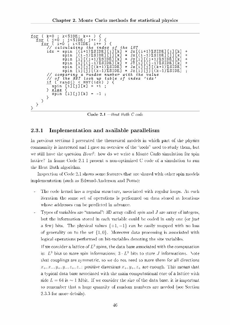
Chapter 2. Monte Carlo methods for statistical physics
for ( k=0 ; k<SIDE; k++ ) {for ( j=0 ; j<SIDE; j++ ) {
for ( i=0 ; i<SIDE; i++ ) {// calculating the index of the LUTidx = spin [(i+1)% SIDE][j][k] * Jx[(i+1)% SIDE][j][k] +
spin [(i-1)% SIDE][j][k] * Jx[(i-1)% SIDE][j][k] +spin [i][(j+1)% SIDE][k] * Jy[i][(j+1)% SIDE][k] +spin [i][(j-1)% SIDE][k] * JY[i][(j-1)% SIDE][k] +spin [i][j][(k+1)% SIDE] * Jz[i][j][(k+1)% SIDE] +spin [i][j][(k-1)% SIDE] * Jz[i][j][(k-1)% SIDE] ;
// comparing a random number with the value// of the HBT look up table of index 'idx'if ( rand() < HBT(idx) ) {
spin [i][j][k] = +1 ;} else {
spin [i][j][k] = -1 ;}
}}
}
Code 2.1 � Heat Bath C code
2.3.1 Implementation and available parallelism
In previous sections I presented the theoretical models in which part of the physics
community is interested and I gave an overview of the �tools� used to study them, but
we still have the question How? : how do we write a Monte Carlo simulation for spin
lattice? In frame Code 2.1 I present a non-optimized C code of a simulation to run
the Heat Bath algorithm.
Inspection of Code 2.1 shows some features that are shared with other spin models
implementation (such as Edward-Anderson and Potts):
- The code kernel has a regular structure, associated with regular loops. At each
iteration the same set of operations is performed on data stored at locations
whose addresses can be predicted in advance.
- Types of variables are �unusual�: 3D array called spin and J are array of integers,
but the information stored in each variable could be coded in only one (or just
a few) bits. The physical values {+1,−1} can be easily mapped with no loss
of generality on to the set {1, 0}. Moreover data processing is associated with
logical operations performed on bit-variables denoting the site variables.
- If we consider a lattice of L3 spins, the data base associated with the computation
is: L3 bits to store spin informations; 3 · L3 bits to store J informations. Note
that couplings are symmetric, so we do not need to store them for all directions
x+, x−, y+, y−, z+, z−: positive directions x+, y+, z+ are enough. This means that
a typical data base associated with the main computational core of a lattice with
side L = 64 is ∼ 1 Mbit. If we consider the size of the data base, it is important
to remember that a huge quantity of random numbers are needed (see Section
2.3.3 for more details).
46
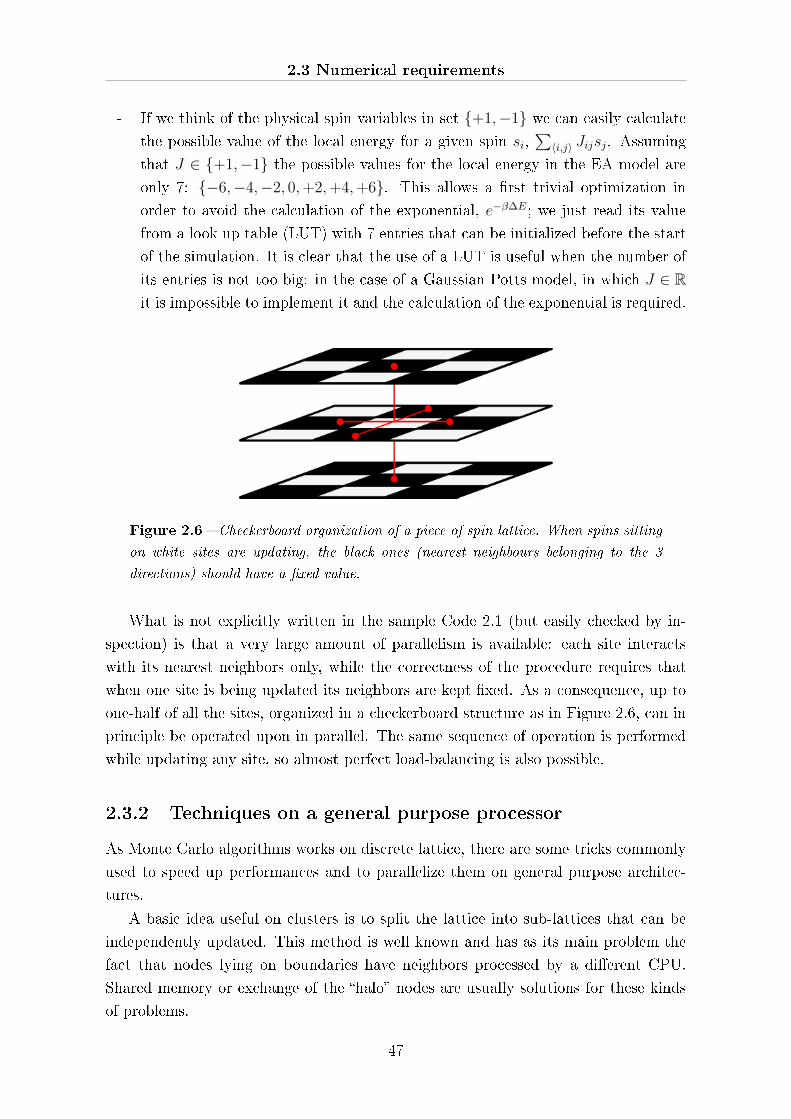
2.3 Numerical requirements
- If we think of the physical spin variables in set {+1,−1} we can easily calculate
the possible value of the local energy for a given spin si,∑〈i,j〉 Jijsj. Assuming
that J ∈ {+1,−1} the possible values for the local energy in the EA model are
only 7: {−6,−4,−2, 0,+2,+4,+6}. This allows a �rst trivial optimization in
order to avoid the calculation of the exponential, e−β∆E; we just read its value
from a look up table (LUT) with 7 entries that can be initialized before the start
of the simulation. It is clear that the use of a LUT is useful when the number of
its entries is not too big: in the case of a Gaussian Potts model, in which J ∈ Rit is impossible to implement it and the calculation of the exponential is required.
Figure 2.6 � Checkerboard organization of a piece of spin lattice. When spins sitting
on white sites are updating, the black ones (nearest neighbours belonging to the 3
directions) should have a �xed value.
What is not explicitly written in the sample Code 2.1 (but easily checked by in-
spection) is that a very large amount of parallelism is available: each site interacts
with its nearest neighbors only, while the correctness of the procedure requires that
when one site is being updated its neighbors are kept �xed. As a consequence, up to
one-half of all the sites, organized in a checkerboard structure as in Figure 2.6, can in
principle be operated upon in parallel. The same sequence of operation is performed
while updating any site, so almost perfect load-balancing is also possible.
2.3.2 Techniques on a general purpose processor
As Monte Carlo algorithms works on discrete lattice, there are some tricks commonly
used to speed up performances and to parallelize them on general purpose architec-
tures.
A basic idea useful on clusters is to split the lattice into sub-lattices that can be
independently updated. This method is well known and has as its main problem the
fact that nodes lying on boundaries have neighbors processed by a di�erent CPU.
Shared memory or exchange of the �halo� nodes are usually solutions for these kinds
of problems.
47
Chapter 2. Monte Carlo methods for statistical physics
In the case of the spin glass simulation we saw e.g. in Figure 2.6 that up to L3/2
spins can be updated concurrently, thus a high level of parallelism is available also
while the update process is running. Today multi-core and SIMD processors are widely
available and, as they can support a high level of parallelism, it seems interesting to
try to port to them using the Metropolis algorithm described above. The technique
used to reach this goal is the multispin coding [31, 32, 33, 34] which stores the states
of several variables (spins in the case of the spin models) in the bits of a single word
of data. So the Monte Carlo algorithm is written in terms of operations which act on
an entire word at a time. The result is that it is possible to perform operations on
several variables at once, rather than performing them sequentially, which improves
the speed of our calculation, thereby giving us better results for a given investment in
CPU time.
We will consider the recently introduced IBM CBE and Intel Nehalem architec-
ture as representative examples of a class of multi-core processors with the following
features:
- a small set of cores are integrated on a single processor.
- Each core support SIMD-like vector instructions operating onW -bit vector data-
words. Each vector data-word can be partitioned in two or more scalar data-words
of di�erent sizes.
- each core has access to a local private memory.
- each core can access data stored on the private memories of the other cores.
- all cores share (arbitrarily) large main memory external to the chip.
- memory accesses and data-transfers can be performed concurrently with compu-
tation.
- memory access performance has a strong dependence on �distance�: latency to
the local memory is constant and small. Access to the local memories of the other
cores has a signi�cantly longer latency, while access to the shared memory is still
much slower.
It is possible to evaluate the performance of a program in terms of spin update
time: the time required to update a single spin of a given system. It is equal to the
wall clock time for a Monte Carlo step divided by L3.
The goal is to exploit the highest possible level of parallelism, so using the highest
granularity of the architecture allows one to update the highest number of spins in
parallel. We need in principle only one bit of the smallest available scalar variable,
the spin, (or few bits in the case of the Potts model), so a large amount of memory
is wasted. For example, if the architecture allows the use of V bytes in parallel, then
7 × V bits are not used, and more generally, if scalar variables are w bit long, then
(w − 1)× V bits are wasted.
48
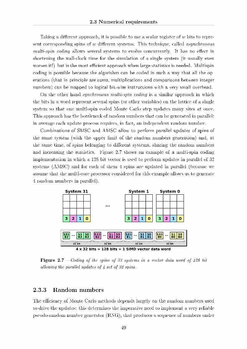
2.3 Numerical requirements
Taking a di�erent approach, it is possible to use a scalar register of w bits to repre-
sent corresponding spins of w di�erent systems. This technique, called asynchronous
multi-spin coding allows several systems to evolve concurrently. It has no e�ect in
shortening the wall-clock time for the simulation of a single system (it usually even
worsen it!) but is the most e�cient approach when large statistics is needed. Multispin
coding is possible because the algorithm can be coded in such a way that all the op-
erations (that in principle are sums, multiplications and comparisons between integer
numbers) can be mapped to logical bit-wise instructions with a very small overhead.
On the other hand synchronous multi-spin coding is a similar approach in which
the bits in a word represent several spins (or other variables) on the lattice of a single
system so that one multi-spin coded Monte Carlo step updates many sites at once.
This approach has the bottleneck of random numbers that can be generated in parallel:
in average each update process requires, in fact, an independent random number.
Combinations of SMSC and AMSC allow to perform parallel updates of spins of
the same system (with the upper limit of the random numbers generation) and, at
the same time, of spins belonging to di�erent systems, sharing the random numbers
and increasing the statistics. Figure 2.7 shows an example of a multi-spin coding
implementation in which a 128 bit vector is used to perform updates in parallel of 32
systems (AMSC) and for each of them 4 spins are updated in parallel (because we
assume that the multi-core processor considered for this example allows us to generate
4 random numbers in parallel).
Figure 2.7 � Coding of the spins of 32 systems in a vector data word of 128 bit
allowing the parallel updates of 4 set of 32 spins.
2.3.3 Random numbers
The e�ciency of Monte Carlo methods depends largely on the random numbers used
to drive the updates: this determines the imperative need to implement a very reliable
pseudo-random number generator (RNG), that produces a sequence of numbers under
49
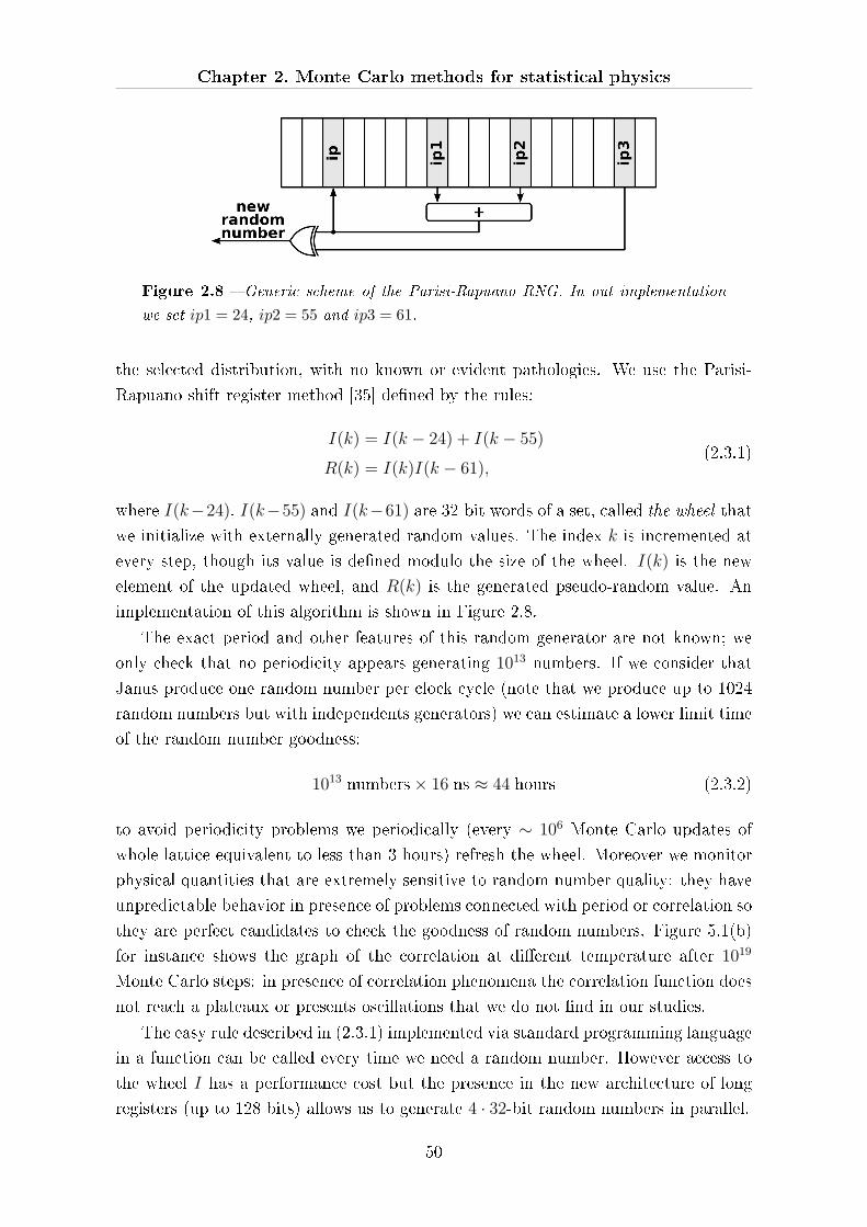
Chapter 2. Monte Carlo methods for statistical physics
Figure 2.8 � Generic scheme of the Parisi-Rapuano RNG. In out implementation
we set ip1 = 24, ip2 = 55 and ip3 = 61.
the selected distribution, with no known or evident pathologies. We use the Parisi-
Rapuano shift register method [35] de�ned by the rules:
I(k) = I(k − 24) + I(k − 55)
R(k) = I(k)I(k − 61),(2.3.1)
where I(k−24), I(k−55) and I(k−61) are 32-bit words of a set, called the wheel that
we initialize with externally generated random values. The index k is incremented at
every step, though its value is de�ned modulo the size of the wheel. I(k) is the new
element of the updated wheel, and R(k) is the generated pseudo-random value. An
implementation of this algorithm is shown in Figure 2.8.
The exact period and other features of this random generator are not known; we
only check that no periodicity appears generating 1013 numbers. If we consider that
Janus produce one random number per clock cycle (note that we produce up to 1024
random numbers but with independents generators) we can estimate a lower limit time
of the random number goodness:
1013 numbers× 16 ns ≈ 44 hours (2.3.2)
to avoid periodicity problems we periodically (every ∼ 106 Monte Carlo updates of
whole lattice equivalent to less than 3 hours) refresh the wheel. Moreover we monitor
physical quantities that are extremely sensitive to random number quality: they have
unpredictable behavior in presence of problems connected with period or correlation so
they are perfect candidates to check the goodness of random numbers. Figure 5.1(b)
for instance shows the graph of the correlation at di�erent temperature after 1019
Monte Carlo steps: in presence of correlation phenomena the correlation function does
not reach a plateaux or presents oscillations that we do not �nd in our studies.
The easy rule described in (2.3.1) implemented via standard programming language
in a function can be called every time we need a random number. However access to
the wheel I has a performance cost but the presence in the new architecture of long
registers (up to 128 bits) allows us to generate 4 · 32-bit random numbers in parallel.
50
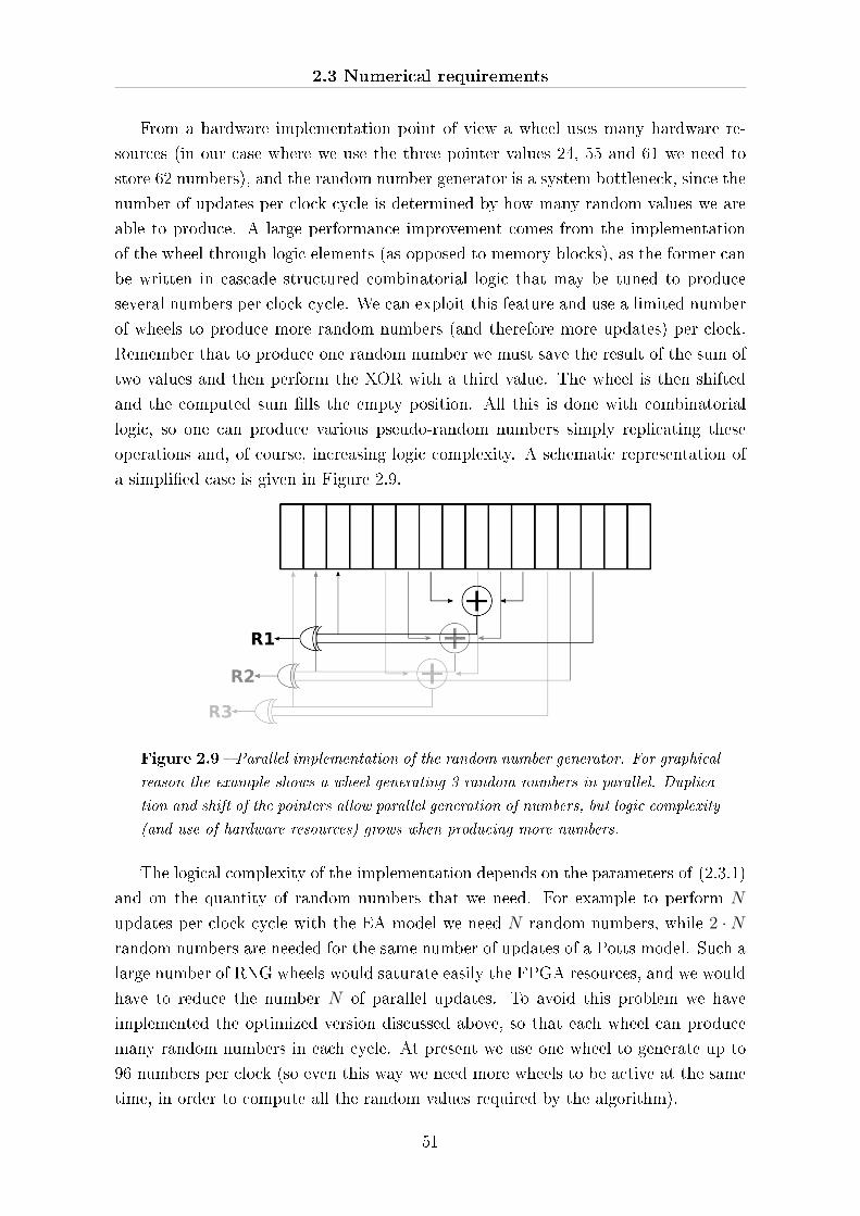
2.3 Numerical requirements
From a hardware implementation point of view a wheel uses many hardware re-
sources (in our case where we use the three pointer values 24, 55 and 61 we need to
store 62 numbers), and the random number generator is a system bottleneck, since the
number of updates per clock cycle is determined by how many random values we are
able to produce. A large performance improvement comes from the implementation
of the wheel through logic elements (as opposed to memory blocks), as the former can
be written in cascade structured combinatorial logic that may be tuned to produce
several numbers per clock cycle. We can exploit this feature and use a limited number
of wheels to produce more random numbers (and therefore more updates) per clock.
Remember that to produce one random number we must save the result of the sum of
two values and then perform the XOR with a third value. The wheel is then shifted
and the computed sum �lls the empty position. All this is done with combinatorial
logic, so one can produce various pseudo-random numbers simply replicating these
operations and, of course, increasing logic complexity. A schematic representation of
a simpli�ed case is given in Figure 2.9.
Figure 2.9 � Parallel implementation of the random number generator. For graphical
reason the example shows a wheel generating 3 random numbers in parallel. Duplica-
tion and shift of the pointers allow parallel generation of numbers, but logic complexity
(and use of hardware resources) grows when producing more numbers.
The logical complexity of the implementation depends on the parameters of (2.3.1)
and on the quantity of random numbers that we need. For example to perform N
updates per clock cycle with the EA model we need N random numbers, while 2 ·Nrandom numbers are needed for the same number of updates of a Potts model. Such a
large number of RNG wheels would saturate easily the FPGA resources, and we would
have to reduce the number N of parallel updates. To avoid this problem we have
implemented the optimized version discussed above, so that each wheel can produce
many random numbers in each cycle. At present we use one wheel to generate up to
96 numbers per clock (so even this way we need more wheels to be active at the same
time, in order to compute all the random values required by the algorithm).
51
Chapter 2. Monte Carlo methods for statistical physics
With respect to the choice of 32-bit random numbers, we have veri�ed that this
word size is su�cient for the models that we want to simulate. Indeed we compare
random numbers with transition probabilities calculated as U = e−β∆Ei where β is the
inverse of the temperature and ∆Ei = Es′i − Esienergy �uctuation after an update
step calculated as in (2.2.15). Typical values assumed by β are ∼ 1 (see values in
Section 5.2). We can therefore calculate the smallest value U corresponding to the
biggest value of energy variation ∆E:
∆E = 12 → e−12 ≈ 6 · 10−6 (2.3.3)
The number of bits to write the integer representation of ∆E is
Nb(∆E) = log2 6 · 106 ≈ 22 bits .
If we consider an error of 10% the random number should be able to represent a
number roughly hundred times smaller than the smallest energy di�erence, so it needs
Nb(R) = log2 6 · 108 ≈ 29 bits .
Mainly we use on Janus 32 bits to be compliant with standard computer systems.
Other models may require larger (i.e. with more bits) random numbers. Generating
random numbers of larger size (e.g., 40 or even 64-bit) is rather straightforward, at the
price, of course, of a larger resource usage, which implies a reduced number of parallel
updates. Obviously the same problem would a�ect PC simulations as well. Most of
the models studied so far have been simulated with 32-bit random numbers.
52
Bibliography
[1] D. P. Landau, K. Binder, A Guide to Monte Carlo Simulations in Statistical
Physics, Cambridge University Press (2005). 2
[2] M. E. J. Newman, G. T. Barkema, Monte Carlo Methods in Statistical Physics,
Oxford University Press (1999). 2
[3] D. Sciretti, Spin Glasses, Protein Design and Dedicated Computers, PhD thesis,
Instituto de Biocomputación y Física de Sistemas Complejos (2008). 2, 2.2
[4] M. Mézard, G. Parisi and M. A. Virasoro, Spin glass theory and beyond, World
Scienti�c, Singapore (1987). 2.1.1, 2.1.2
[5] F. Guerra, Broken Replica Symmetry Bounds in the Mean Field Spin Glass Model,
Commun. Math. Phys. 233, pp. 1-12 (2003). 2.1.1
[6] M. Talagrand, The Parisi formula, Annals of Mathematics, 163, 221-263 (2006).
2.1.1
[7] G. Parisi, F. Zamponi, Replica approach to glass transition and jammed states of
hard spheres, arXiv:0802.2180v1, (2008). 2.1.1
[8] D. Sherrington and S. Kirkpatrick, Solvable Model of a Spin-Glass, Phys. Rev.
Lett. 35, 1792 (1975). 2.1.2
[9] R. K. Zia and D. J. Wallace, Critical behaviour of the continuous n-component
Potts model, J. Phys. A, 8, pp. 1495-1507 (1975) 2.1.3
[10] J. Banavar and M. Cieplak, Zero-temperature scaling for Potts spin glasses, Phys.
Rev. B 39, 9633 (1989). 2.1.3
[11] M. Scheucher and J. D. Reger, Monte Carlo study of the bimodal three-state Potts
glass, Phys. Rev. B 45, 2499 (1992). 2.1.3
[12] L. W. Lee, H. G. Katzgraber and A. P. Young, Critical behavior of the three- and
ten-state short-range Potts glass: A Monte Carlo study, Phys. Rev. B 74, 104416
(2006). 2.1.3
53
BIBLIOGRAPHY
[13] P. Erdös, A. Rényi, On random graphs, Publicationes Mathematicae, 6, 290-297
(1959). On the evolution of random graphs, Publications of the Mathematical
Institute of the Hungarian Academy of Sciences 5, 17Â61 (1960). 2.1.3
[14] B. Bollobàs, P. Erdös, Cliques in Random Graphs, Math. Proc. Cambridge Phil.
Soc. 80, 3, pp. 419-427 (1976). 2.1.3
[15] B. Bolloboàs, Random Graphs (2nd ed.), Cambridge University Press (2001). 2.1.3
[16] A. D. Sokal, Chromatic polynomials, Potts models and all that, Physica A: Sta-
tistical Mechanics and its Applications, Vol. 279, Issues 1-4, pp. 324-332 (2000).
2.1.3
[17] L. Zdeborová and F. Krzakala, Phase transitions in the coloring of random graphs,
Phys. Rev. E 76, 031131 (2007). 2.1.3
[18] F. Krzakala and L. Zdeborová, Potts glass on random graphs, EPL 81, n. 5, 57005
(2008). 2.1.3
[19] F. Mantovani, Graph Coloring on IANUS, an FPGA Based System, poster pre-
sented at the International Supercomputing Conference 2007 (ISC07), Dresden
(Germany). 2.1.3
[20] E. Marinari et al., Programmazione scienti�ca, linguaggio C, algoritmi e modelli
nella scienza, Pearson Education Italia (2006). 2.4
[21] M. Metropolis et al., Equations of state calculations by fast computing machines,
Journal of Chemical Physics, 21, pp. 1087-1092 (1953). 2.2.3, 2.2.3, 2.2.3
[22] W. K. Hastings, Monte Carlo sampling methods using Markov chains and their
applications Biometrika, 57:92-109 (1970). 2.2.3
[23] C. P. Robert and G. Casella, Monte Carlo Statistical Methods, Springer, New
York, 2nd edition (2004). 2.2.3, 2.2.3
[24] E. H. L. Aarts and J. H. M. Korst, Simulated Annealing and Boltzmann Machines,
John Wiley & Sons, Chichester (1989). 2.2.3
[25] E. Marinari, in Advances in Computer Simulations, ed. J. Kertèsz and I. Kondor,
Springer, 50 (1996). 2.2.6
[26] K. Hukushima and K. Nemoto, Exchange Monte Carlo method and application to
spin glass simulations, J. Phys. Soc. Japan, Vol. 65, 1604 (1996). 2.2.6
[27] R. H. Swendsen and J. S. Wang, Replica Monte Carlo Simulation of Spin-Glasses,
Phys. Rev. Lett. 57, 2607 (1986). 2.2.6
54
BIBLIOGRAPHY
[28] C. J. Geyer, Computing Science and Statistics: Proc. 23rd Symp. on the Interface,
156 (1991). 2.2.6
[29] H. G. Katzgraber et al., Feedback-optimized parallel tempering Monte Carlo, J.
Stat. Mech., P03018, (2006). 2.2.6
[30] S. Trebst et al., Optimizing the ensemble for equilibration in broad-histogram
Monte Carlo simulations, Phys. Rev. E 70, 046701 (2004). 2.2.6
[31] M. Creutz, L. Jacobs and C. Rebbi, Experiments with a Gauge-Invariant Ising
System, Phys. Rev. Lett. 42, 1390 (1979). 2.3.2
[32] R. Zorn, H. J. Herrmann and C. Rebbi, Tests of the multi-spin-coding technique
in Monte Carlo simulations of statistical systems, Computer Physics Communi-
cations, Vol. 23, Issue 4, pp. 337-342 (1981). 2.3.2
[33] G. O. Williams and M. H. Kalos, A new multispin coding algorithm for Monte
Carlo simulation of the Ising model, J. Stat. Phys. 37, pp. 283-299 (1984). 2.3.2
[34] P. M. C. de Olivieira, Computing Boolean Statistical Models, World Scienti�c
(1991). 2.3.2
[35] G. Parisi, F. Rapuano, E�ects of the random number generator on computer
simulations, Phys. Lett. B 157, 301 (1985). 2.3.3
55

We gotta get out while we're young
'cause tramps like us, baby we were born to run.
Bruce Springsteen
3Janus architecture at large
In this chapter I introduce the Janus project and the FPGA-based system built at the
heart of it. A short introductive section is dedicated to explain the structure of the
system, the main components and their functions.
After highlighting the Janus system the idea is to retrace the architectural questions
that led to the Janus systems and were solved by me and my group in Ferrara during
prototype and development phase of Janus (the main activity of my PhD). Therefore
a relatively long part of this chapter will be dedicated to a detailed overview of the
problems connected to the development of a massively parallel dedicated machine such
as Janus.
The last three sections are dedicated to the hardware implementation of two sta-
tistical physics models: the Edward Anderson spin glass model, the spin model using
the parallel tempering technique and the Potts model on an irregular lattice, the
last one with the main aim to solve the graph coloring problem. The theoretical de-
tails of these problems were introduced in previous chapter, therefore they are here
presented in terms of their implementation in a hardware description language on a
programmable device.
Details about input output, control system, �rmware, VHDL code etc. are post-
poned to the next chapter in order to keep here general ideas strongly connected
with the needs that encourage an heterogeneous group of physicists, mathematicians
and computer scientist to build a dedicated machine not only in order to solve open
problems of statistical physics but also to study new architectural solutions and new
57
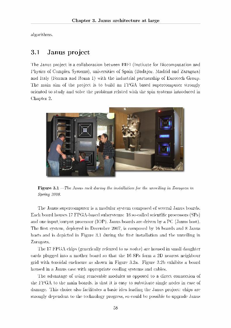
Chapter 3. Janus architecture at large
algorithms.
3.1 Janus project
The Janus project is a collaboration between BIFI (Institute for Biocomputation and
Physics of Complex Systems), universities of Spain (Badajoz, Madrid and Zaragoza)
and Italy (Ferrara and Roma 1) with the industrial partnership of Eurotech Group.
The main aim of the project is to build an FPGA based supercomputer strongly
oriented to study and solve the problems related with the spin systems introduced in
Chapter 2.
Figure 3.1 � The Janus rack during the installation for the unveiling in Zaragoza in
Spring 2008.
The Janus supercomputer is a modular system composed of several Janus boards.
Each board houses 17 FPGA-based subsystems: 16 so-called scienti�c processors (SPs)
and one input/output processor (IOP). Janus boards are driven by a PC (Janus host).
The �rst system, deployed in December 2007, is composed by 16 boards and 8 Janus
hosts and is depicted in Figure 3.1 during the �rst installation and the unveiling in
Zaragoza.
The 17 FPGA chips (generically referred to as nodes) are housed in small daughter
cards plugged into a mother board so that the 16 SPs form a 2D nearest neighbour
grid with toroidal enclosure as shown in Figure 3.2a. Figure 3.2b exhibits a board
housed in a Janus case with appropriate cooling systems and cables.
The advantage of using removable modules as opposed to a direct connection of
the FPGA to the main boards, is that it is easy to substitute single nodes in case of
damage. This choice also facilitates a basic idea leading the Janus project: chips are
strongly dependent to the technology progress, so could be possible to upgrade Janus
58
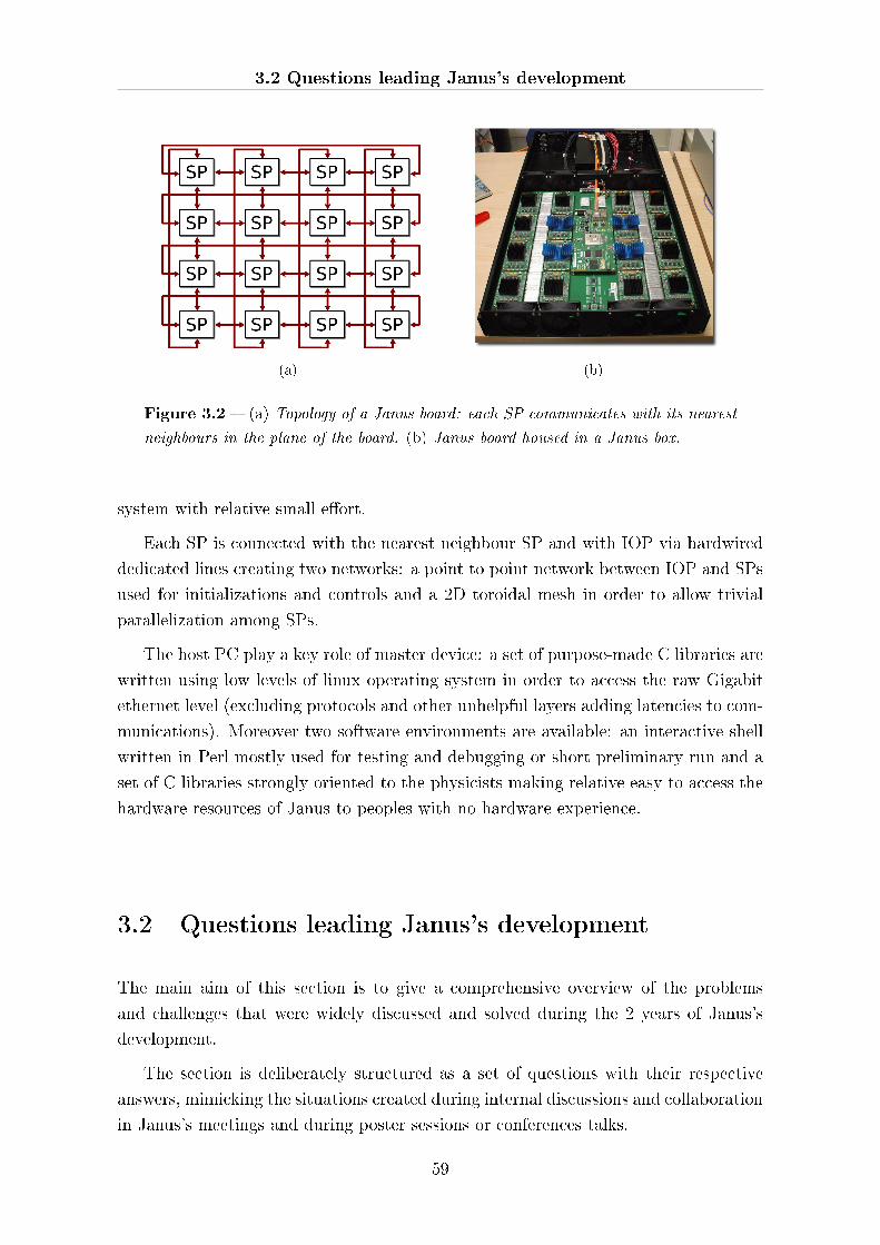
3.2 Questions leading Janus's development
(a) (b)
Figure 3.2 � (a) Topology of a Janus board: each SP communicates with its nearest
neighbours in the plane of the board. (b) Janus board housed in a Janus box.
system with relative small e�ort.
Each SP is connected with the nearest neighbour SP and with IOP via hardwired
dedicated lines creating two networks: a point to point network between IOP and SPs
used for initializations and controls and a 2D toroidal mesh in order to allow trivial
parallelization among SPs.
The host PC play a key role of master device: a set of purpose-made C libraries are
written using low levels of linux operating system in order to access the raw Gigabit
ethernet level (excluding protocols and other unhelpful layers adding latencies to com-
munications). Moreover two software environments are available: an interactive shell
written in Perl mostly used for testing and debugging or short preliminary run and a
set of C libraries strongly oriented to the physicists making relative easy to access the
hardware resources of Janus to peoples with no hardware experience.
3.2 Questions leading Janus's development
The main aim of this section is to give a comprehensive overview of the problems
and challenges that were widely discussed and solved during the 2 years of Janus's
development.
The section is deliberately structured as a set of questions with their respective
answers, mimicking the situations created during internal discussions and collaboration
in Janus's meetings and during poster sessions or conferences talks.
59

Chapter 3. Janus architecture at large
3.2.1 Why many nodes on a board?
There are three primary classes of techniques for creating a parallel algorithm to
perform a simulation on a d-dimensional lattice: trivial parallelization, functional
decomposition and domain decomposition.
Trivially parallel problems are ones which can be split up into separate tasks which
are completely unrelated and can be performed by separate programs running on
isolated processors without the need for inter-processor communication.
For more complicated problems we have two ways to go. Functional decomposition
refers to the breaking up of a task into a variety of di�erent jobs: each processor in
a program which carries out such a task is performing a di�erent type of work, and
the contributions of all the processors put together perform the complete task. We
could imagine for example delegating separate processors in a Monte Carlo calculation
to evaluation of a Hamiltonian or other observable, construction of clusters, updating
lattice variables, or any number of other elementary chores. This however is not a
very common approach to the kinds of calculations needed in parallel systems such as
Janus.
Monte Carlo simulations almost always use domain decomposition, which means
breaking up the calculation into separate simulations of di�erent regions of the sys-
tem under study. Since Monte Carlo simulations are usually concerned with systems
de�ned on a lattice this approach is often quite straightforward to implement. The
processors in such a calculation all perform essentially the same task on di�erent parts
of the lattice, and indeed are often running exactly the same program.
Following this general idea, Janus is structured as a collection of FPGA-based
processors, running the same �rmware, able to process each one a portion of a given
lattice.
3.2.2 Why an Input/Output processor?
In computer science is widely use the concept of loose coupling referring to a relation-
ship in which one module interacts with another module through a stable interface
and does not need to be concerned with internal implementation of other modules. In
this de�nition the term module is su�ciently general to encompass functions of a high
level language, or hardware components such as a CPU or an FPGA. Conversely when
interaction of two modules requires informations about their implementation, we are
in presence of tight coupling.
Systems that do not exhibit tight coupling might experience the following devel-
opmental di�culties:
- Change in one module forces a ripple of changes in other modules.
- Modules are di�cult to understand in isolation.
60
3.2 Questions leading Janus's development
- Modules are di�cult to reuse or test because dependent modules must be in-
cluded.
The basic idea for Janus was to develop a loosely coupled machine in which the
Janus host (intended as a module) should interact with SPs while ignoring in principle
the algorithm implemented within the FPGA. This statement was a guide in the
development of the Janus hardware and for this reason we chose to develop a custom
Input/Output Processor, IOP, to play the key role of a stable interface between the
Janus host and SPs, thus assuring the loose coupling between them.
It is clear that the development of an interface module is not the only way to
e�ciently realize a loosely coupled machine: e.g. Maxwell uses the PCI buses to allow
communications between the general purpose processors and the FPGAs constituting
the system.
The choice of a custom module such as IOP comes from features of the class of
algorithms that we plan to run on Janus: Monte Carlo simulations for spin lattices
requires in fact a small data exchange with relative low latency and very long run
time. If we consider, for instance, a spin lattice of side L = 64, the data to transfer
from the Janus host to the SP in order to start a simulations is: L3 bits for the spins,
3 · L3 bits for the Js, 7 words of 32 bits in order to initialize the LUT of the energies
and 61 words of 32 bits for initializing of the random number generator.
643 + (3 · 643) + (7 · 32) + (61 · 32) ≈ 1Mbits
If we consider the worst case in which each SP run a completely di�erent history to
the others, we have to transfer ∼ 16 Mbit (2 MB) from the Janus host to each of the
FPGA structures storing data. Another Janus requirement could be to upload new
�rmware for the SPs: this requires a transfer of ∼ 5 MB.
So we have that typical bandwidth requirements are of the order of some MB,
therefore relatively small, but what are the latency requirements? Some Monte Carlo
techniques requires that every P Monte Carlo steps spin con�gurations (or alterna-
tively LUT) are changed using a simple rule depending on the temperature (parallel
tempering). In such cases is very important to have a large bandwidth, but much
more important is a low latency in order to exchange e�ciently the con�guration and
so not waste computing time.
3.2.3 How are organized communications between Janus boards
and Janus host?
The programming framework developed for Janus is intended to meet the requirements
of the prevailing operating modes of Janus, i.e. supporting (re)con�guration of SPs,
61

Chapter 3. Janus architecture at large
Figure 3.3 � Framework of an application running on the Janus system.
initialization of memories and data structures within the FPGA, a monitor system
during run, memory interface and some other debug functions.
Applications running on the Janus system can be thought of as split into two sub-
applications, one, called software application SA, written for example in C, and running
on the Janus host. The other, called �rmware application FA, written for example in
VHDL, and running on the nodes of a Janus board. As shown in Figure 3.3, the two
entities, SA and FA are connected together by a communication infrastructure CI,
that is a logical block including physically the IOP and which allows the exchange of
data and performs synchronization operations, directly and in a transparent way.
The CI abstracts the low-level communication between SA and FA applications,
implemented in hardware by the IOP and its interfaces. It includes three main com-
ponents:
- a C communication library linked by the SA,
- a communication �rmware running on the IOP processor, interfacing both the
host PC and the SP processor,
- a VHDL library linked by the FA.
Firmware running on the IOP communicates with the host PC via a dual Gigabit
channel, using the standard RAW-ethernet communication protocol. The choice of
RAW-ethernet is based on the following considerations:
- the standard TCP/IP protocol provides a lot of functionalities which are not
needed by our purposes;
- an hardware implementation of the TCP/IP stack is non trivial, uses far more
hardware resources and is more time critical than a RAW-ethernet implementa-
tion;
- the TCP/IP protocol introduces overheads in the communication.
To guarantee reliability of the communication in the direction IOP to Janus host,
we adopt the Go-back-N protocol [1]. In this protocol, N frames are sent without
waiting for an acknowledge from the receiver. After N frames have been transmitted,
the sender waits for an acknowledge. If the acknowledge is positive it starts to send
62
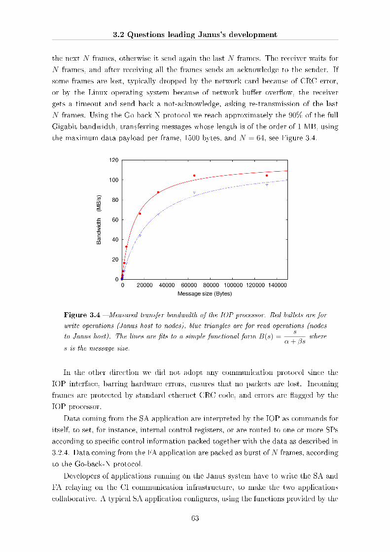
3.2 Questions leading Janus's development
the next N frames, otherwise it send again the last N frames. The receiver waits for
N frames, and after receiving all the frames sends an acknowledge to the sender. If
some frames are lost, typically dropped by the network card because of CRC error,
or by the Linux operating system because of network bu�er over�ow, the receiver
gets a timeout and send back a not-acknowledge, asking re-transmission of the last
N frames. Using the Go-back-N protocol we reach approximately the 90% of the full
Gigabit bandwidth, transferring messages whose length is of the order of 1 MB, using
the maximum data payload per frame, 1500 bytes, and N = 64, see Figure 3.4.
Figure 3.4 � Measured transfer bandwidth of the IOP processor. Red bullets are for
write operations (Janus host to nodes), blue triangles are for read operations (nodes
to Janus host). The lines are �ts to a simple functional form B(s) =s
α+ βswhere
s is the message size.
In the other direction we did not adopt any communication protocol since the
IOP interface, barring hardware errors, ensures that no packets are lost. Incoming
frames are protected by standard ethernet CRC code, and errors are �agged by the
IOP processor.
Data coming from the SA application are interpreted by the IOP as commands for
itself, to set, for instance, internal control registers, or are routed to one or more SPs
according to speci�c control information packed together with the data as described in
3.2.4. Data coming from the FA application are packed as burst of N frames, according
to the Go-back-N protocol.
Developers of applications running on the Janus system have to write the SA and
FA relaying on the CI communication infrastructure, to make the two applications
collaborative. A typical SA application con�gures, using the functions provided by the
63
Chapter 3. Janus architecture at large
communication library, the SP processors with the �rmware corresponding to the FA
program, loads input data for the FA application, and it waits for the incoming results.
On the other side, a typical FA application wait for incoming requests, performs some
calculation and sends back the results.
The approach adopted to develop application for the Janus system explained in
this section is to keep deliberately the structure of the IOP as easy as possible in order
to have a low latency stable (and hopefully standard) interface between SA running
on Janus host and FA running on SPs. This approach is coherent to the concept of
loose coupling introduced in 3.2.2 and could allow the use of development toolkits to
automatically decompose an application into cooperating modules.
3.2.4 How are organized communications within a Janus board?
The current �rmware con�guration of the IOP focuses on the implementation of an
interface between SPs and Janus host. Although a programmable device is used to
implement it, IOP is not intended as a recon�gurable processor: it basically allows
streaming of data from the host to the appropriate destination (and back), under the
complete control of the Janus host and its con�guration should remain �xed.
The IOP con�gured structure is naturally split into 2 worlds:
- IOlink block handles the I/O interfaces between IOP and host-PC (Gigabit chan-
nels, serial and USB ports). Its supports the lower layers of the Gigabit ethernet
protocol, ensures data integrity and provides a bandwidth close to the theoretical
limit;
- multidev block contains a logical device associated with each hardware subsystem
that may be reached for control and/or data transfer: there is a memory interface
for the staging memory, a programming interface to con�gure the SPs, an SP
interface to handle communication with the SPs (after they are con�gured) and
several service/debug interfaces.
A block diagram of the IOP is shown in Figure 3.5.
Gigabit ethernet feeds the IOlink with a stream composed of 32 bit words with a
clock period of 8 ns (125 MHz). Internal entities of the IOlink synchronize the stream
and return a 16 bit data stream (dataIn) and a data valid (dvIn) clocked by the main
system clock with a period of 16 ns (62.5 MHz). See section 3.2.9 for more detail about
clock frequencies.
In order to route the input stream coming from IOlink we considered three di�erent
possibilities explained in detail in Appendix A. All three ideas that we considered use
a module Stream Router, SR that scans the data stream, recognizes a �speci�c� semi-
word associated with a device and sets high a valid signal for the device selection
(devSelVal).
64
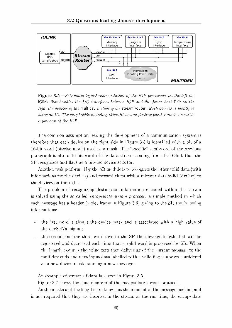
3.2 Questions leading Janus's development
Figure 3.5 � Schematic logical representation of the IOP processor: on the left the
IOlink that handles the I/O interfaces between IOP and the Janus host PC; on the
right the devices of the multidev including the streamRouter. Each devices is identi�ed
using an ID. The gray bubble including MicroBlaze and �oating point units is a possible
expansion of the IOP.
The common assumption leading the development of a communication system is
therefore that each device on the right side in Figure 3.5 is identi�ed with a bit of a
16-bit word (bitwise mode) used as a mask. The �speci�c� semi-word of the previous
paragraph is also a 16 bit word of the data stream coming from the IOlink that the
SP recognizes and �ags as a bitwise device selector.
Another task performed by the SR module is to recognize the other valid data (with
informations for the devices) and forward them with a relevant data valid (dvOut) to
the devices on the right.
The problem of recognizing destination information encoded within the stream
is solved using the so called encapsulate stream protocol : a simple method in which
each message has a header (violet frame in Figure 3.6) giving to the SR the following
informations:
- the �rst word is always the device mask and is associated with a high value of
the devSelVal signal;
- the second and the third word give to the SR the message length that will be
registered and decreased each time that a valid word is processed by SR. When
the length assumes the value zero then delivering of the current message to the
multidev ends and next input data labelled with a valid �ag is always considered
as a new device mask, starting a new message.
An example of stream of data is shown in Figure 3.6.
Figure 3.7 shows the time diagram of the encapsulate stream protocol.
As the masks and the lengths are known at the moment of the message packing and
is not required that they are inserted in the stream at the run time, the encapsulate
65
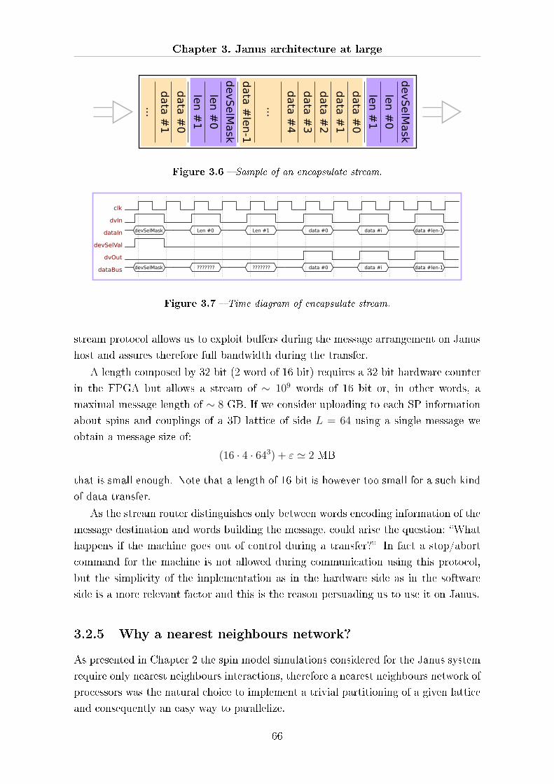
Chapter 3. Janus architecture at large
Figure 3.6 � Sample of an encapsulate stream.
Figure 3.7 � Time diagram of encapsulate stream.
stream protocol allows us to exploit bu�ers during the message arrangement on Janus
host and assures therefore full bandwidth during the transfer.
A length composed by 32 bit (2 word of 16 bit) requires a 32 bit hardware counter
in the FPGA but allows a stream of ∼ 109 words of 16 bit or, in other words, a
maximal message length of ∼ 8 GB. If we consider uploading to each SP information
about spins and couplings of a 3D lattice of side L = 64 using a single message we
obtain a message size of:
(16 · 4 · 643) + ε ' 2 MB
that is small enough. Note that a length of 16 bit is however too small for a such kind
of data transfer.
As the stream router distinguishes only between words encoding information of the
message destination and words building the message, could arise the question: �What
happens if the machine goes out of control during a transfer?� In fact a stop/abort
command for the machine is not allowed during communication using this protocol,
but the simplicity of the implementation as in the hardware side as in the software
side is a more relevant factor and this is the reason persuading us to use it on Janus.
3.2.5 Why a nearest neighbours network?
As presented in Chapter 2 the spin model simulations considered for the Janus system
require only nearest neighbours interactions, therefore a nearest neighbours network of
processors was the natural choice to implement a trivial partitioning of a given lattice
and consequently an easy way to parallelize.
66

3.2 Questions leading Janus's development
Following this �rst trivial answer, it is possible to think about the historical rea-
sons that guided the Janus collaboration to realize a such network. In view of the
resources available on Virtex-4 LX160 devices used with the �rst prototype of Janus,
we estimated to be able to update ∼ 100 spins in parallel into a single FPGA. This
led us to think that to simulate a big lattice it would be necessary to split it among
di�erent processors in order to increase ∼ 10 times the parallel spin update rate. The
nearest neighbours networks was therefore needed.
However the use of new FPGAs for the production system (we substitute Virtex-4
LX160 with Virtex-4 LX200) and the introduction of some optimizations in the VHDL
code allowed us to increase by about one order of magnitude the number of parallel
updates performed on a single FPGA so that it is possible to update a stand alone
�big� lattice (i.e. up to 803) in a single node.
3.2.6 Why do boards have no direct link among them self?
There are examples of other parallel dedicated machines composed of standard proces-
sor linked with custom processors housed on boards with di�erent features and goals
(see for instance [2, 3]). In many of these cases each custom processor is considered
as a node of a structured network (e.g. ring, mesh, crossbar, torus), therefore a link
among nodes is required and thus, if nodes are housed on main boards, a link among
boards is necessary. In the case of Janus however the development choice was to avoid
a direct board connection.
Estimated performance for a board equipped with 16 FPGA was enough to jus-
tify the costs of the systems and the adding of a back-plane for the board to board
connections would have increased costs, complexity of design and development time
and could not be justi�ed. As described in [4] in fact, development of a custom and
dedicated machine makes sense if performance obtained and development time are
balanced: increasing the complexity of Janus's design in order to add a direct board
to board connection would have entailed a delay of some months to the delivery of the
system while adding a negligible increase to the performance of the system.
Another reason to leave out board to board connection is the costs that would
have a such architectural choice. A goal of the Janus project was in fact to take part
to the Gordon Bell Prize award as an entry in the cost-e�ciency machine section [5].
Cost-control was therefore a weak development guideline.
In the end the building of a backplane would also con�ict to another idea of the
Janus project, that was to build a modular supercomputer able to run in a rack but
that could be in some sense also portable: a Janus board out of the rack is in fact
∼ 30cm × 30cm and can run connected to a common power plug and linked via a
Gigabit cable to a standard laptop.
67
Chapter 3. Janus architecture at large
3.2.7 Why only 17 nodes per board?
In the development phase of a large system such as Janus it is important to consider
the technology factor, by which we mean studying data sheets and application notes
in order to know the limits and thresholds of the technology that one decides to use.
In the case of an FPGA based system the number of nodes housed in a board is
not arbitrary, but arises from a technology factor. Each SP in fact has a set of 10
hardwired lines connecting it with the IOP and a set of 16 di�erential pairs (32 lines
in all) to exchange data with the nearest neighbours. The number of signals hardwired
in a board is very high and many physical layers are required in order to distribute all
the signals with equalized delays and obtain a completely synchronous system. In the
case of Janus the SP and IOP modules are composed of 12 layers while the mother
board needs 16 layers to allow the wiring of signals.
Another limiting factor is the power supply problem. We decided for Janus to
power each board independently via 48V input voltage in order to be compliant with
most standard industrial power supplies, and distribute this voltage on the main board
and convert it to 2.5V for each node using a DCDC converter. On board each node
we convert than 2.5V to 1.2V so that we have both voltages to power I/O and core of
the FPGA. Distribution and conversion of voltages are critical design factors and core
voltage is a very critical limit for the VHDL design implemented on the FPGA.
The development strategy was a good choice for Janus and the use of consolidated
technology makes the project not overly challenging on the engineering side. Outstand-
ing help came moreover from the ability and experience of employees of Eurotech, the
industrial partner of the Janus project.
3.2.8 Why do the nodes have no o� chip memory?
The question of the on chip vs o� chip memory is a never ending story and an open
question in many large systems. New multi-core architectures, for instance Intel's
Nehalem, adopt a cache level shared among cores and a faster (and smaller) cache
level local for each core. Moreover they integrate on chip a memory controller in order
to speed up access and increase bandwidth to main memory.
In the case of a recon�gurable computer each FPGA o�ers at present up to ∼ 5−8
MB of on chip memory. The choice of the Janus collaboration was to consider this
memory as su�cient and take advantage of the very high bandwidth given by the
fact that the memories were within the FPGA. The reason of this drastic direction
is justi�ed by the fact that the data base of spin glass systems is in any case very
small and embedded memories allow Janus to be a reference machine for these models
for next 5 years. Data base of a spin system of lattice L needs in fact a quantity of
memory of ∼ 4 ·L3 bits. If we search values of L solving the constraint 4 ·L3 < 6 MB
68
3.2 Questions leading Janus's development
we found that the biggest lattice that can be stored within an FPGA has L ' 116.
We suggest therefore that on chip memory is not a limiting factor for simulation of
spin systems on Janus.
The presence of staging memories o� chip introduce the problem of bandwidth
between memory and FPGA that added to the low work frequency of Janus raises a
problem of IO bandwidth related to the packaging of the FPGA. To update N spins
per clock cycle we need in fact to access 4 · N bits and if we suppose N = 256 (a
fourth of the current update rate per clock cycle) we should have a bandwidth of 1024
bits per clock cycle. This is impossible to realize because the number of the IO pins
on an FPGA used for Janus is ∼ 1000. Using a double or quadruple data rate 2 or
4 data words per clock cycle are exchanged with the memory and could be possible
to implement an interface with external memory with an acceptable bandwidth and a
limited usage of IO pins, but part of the logic would need to be used to implement it
and the timing constraints would increase the complexity of the synthesis process. It is
remarkable that all this e�ort is required to achieve a fourth of the actual bandwidth.
If the on chip memory seems enough for the high-e�ciency implementation of the
spin models, a problem arises when we try to implement on Janus a model having a
bigger data base or with an irregular structure. Section 3.5 describes a preliminary
implementation of the random graph coloring problem on Janus and are described
some di�culties encountered to store graph informations within embedded memories.
The choice to build computation nodes with no o� chip memory can be viewed
as an easy way to have a high performance machine for spin systems that on the
downside introduces a limiting factor to the recon�gurability and generality of the
Janus supercomputer.
3.2.9 Which clock frequency and why?
The main board of Janus is equipped with a variable frequency oscillator distributing
a clock signal of 62.5 MHz to each daughter board via equalized lines.
The idea was to use for the Janus nodes a clock frequency not too high in order
to keep the synthesis process of the VHDL code relative easy and non challenging in
terms of time constrains. A low frequency moreover allows one to program a Janus
board as a synchronous system and to consider each FPGA synchronous with each of
the others avoiding tricky synchronization process during data transfer among nodes.
A good compromise frequency was 62.5 MHz directly coming from half of the
Gigabit ethernet work frequency (125 MHz). Therefore we distribute to each FPGA a
62.5 MHz clock and then, only on the IOP with a clock multiplier obtained by built-in
Digital Clock Manager (DCM), we obtain the 125 MHz to use for the I/O.
In this way the bandwidth are completely balanced because Gigabit ethernet pro-
duce 32 bit word each clock cycle (8 ns); Janus distribute words of 16 bits for each
69
Chapter 3. Janus architecture at large
clock cycle, but works at half of the frequency (16 ns per clock cycle) so that the
information distribution is balanced.
A posteriori we discovered that the choice of a low frequency played a key role in
the Janus development. High clock frequency combined with very high density designs
produce in fact a nightmare in terms of power consumption of the FPGAs: In some
cases we obtain in fact the switching o� of the chip after few seconds of run. Because
of this we had to improve the power supply when we decide to adopt Virtex-4 LX200
instead LX160 (more details in 4.2.1 and in 4.2.3).
3.3 SP �rmware: spin glass
3.3.1 Parallelism
The guiding line of our implementation strategy is to try to express all the paralleliza-
tion opportunities allowed by the FPGA architecture, matching as much as possible
the potential for parallelism o�ered by spin systems. Let us start by remembering
that, because of the locality of the spatial interaction [6], the lattice can be split in
two halves in a checkerboard scheme (we are dealing with a so-called bipartite lattice
depicted in �gure Figure 2.6), allowing in principle the parallel update of all white (or
black) sites at once. Additionally, one can further boost performance by updating in
parallel more copies of the system. We do so by updating at the same time two spin
lattices (see later for further comments on this point).
The hardware structure of FPGAs allows exploitation of the full parallelism avail-
able in the algorithm, with the only limit of logic resources. As we explain below, the
FPGAs that we use (Virtex-4 LX160 and Virtex-4 LX200, manufactured by Xilinx)
have enough resources for the simultaneous update of half the sites for lattices of up
to 803 sites. For larger systems there are not enough logic resources to generate all
the random numbers needed by the algorithm (one number per update, see below for
details), so we need more than one clock cycle to update the whole lattice. In other
words, we are in the very rewarding situation in which: i) the algorithm o�ers a large
degree of allowed parallelism, ii) the processor architecture does not introduce any
bottleneck to the actual exploitation of the available parallelism, iii) performance of
the actual implementation is only limited by the hardware resources contained in the
FPGAs.
We have developed a parallel update scheme, supporting 3D lattices with L ≥ 16,
associated with the Hamiltonian of (2.1.4). One only has to tune a few parameters to
adjust the lattice size and the physical parameters de�ned in H. We regard this as an
important �rst step in the direction of creating �exible enough libraries of application
codes for an FPGA-based computers.
70
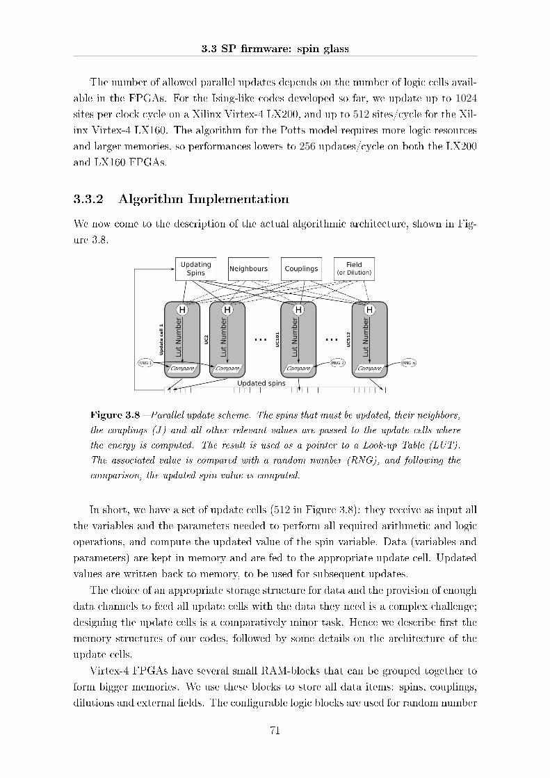
3.3 SP �rmware: spin glass
The number of allowed parallel updates depends on the number of logic cells avail-
able in the FPGAs. For the Ising-like codes developed so far, we update up to 1024
sites per clock cycle on a Xilinx Virtex-4 LX200, and up to 512 sites/cycle for the Xil-
inx Virtex-4 LX160. The algorithm for the Potts model requires more logic resources
and larger memories, so performances lowers to 256 updates/cycle on both the LX200
and LX160 FPGAs.
3.3.2 Algorithm Implementation
We now come to the description of the actual algorithmic architecture, shown in Fig-
ure 3.8.
Figure 3.8 � Parallel update scheme. The spins that must be updated, their neighbors,
the couplings (J) and all other relevant values are passed to the update cells where
the energy is computed. The result is used as a pointer to a Look-up Table (LUT).
The associated value is compared with a random number (RNG), and following the
comparison, the updated spin value is computed.
In short, we have a set of update cells (512 in Figure 3.8): they receive as input all
the variables and the parameters needed to perform all required arithmetic and logic
operations, and compute the updated value of the spin variable. Data (variables and
parameters) are kept in memory and are fed to the appropriate update cell. Updated
values are written back to memory, to be used for subsequent updates.
The choice of an appropriate storage structure for data and the provision of enough
data channels to feed all update cells with the data they need is a complex challenge;
designing the update cells is a comparatively minor task. Hence we describe �rst the
memory structures of our codes, followed by some details on the architecture of the
update cells.
Virtex-4 FPGAs have several small RAM-blocks that can be grouped together to
form bigger memories. We use these blocks to store all data items: spins, couplings,
dilutions and external �elds. The con�gurable logic blocks are used for random number
71

Chapter 3. Janus architecture at large
generators and update cells.
To update one spin of a three dimensional model we need to read its six nearest
neighbors, six couplings, the old spin value (for the Metropolis algorithm) and some
model-dependent information such as a magnetic �eld or a dilution parameter for small
variants of the model. All these data items must be moved to the appropriate update
cells, in spite of the hardware bottleneck that only two memory locations in each block
can be read/written at each clock cycle.
Let us analyze �rst the Ising models, considering for speci�cally the case L = 16.
We choose to use an independent memory of size L3 for each variable. This is actually
divided into smaller memories, arranged so that reading one word from each gives us
all the data needed for a single update cycle. We need 163 = 4096 bits to store all
the spins of one con�guration. We have 16 vertical planes, and save each plane in a
di�erent memory of width 16 bits and height 16 (see Figure 3.9). In this simple case
the logic resources within the FPGA allow us to update one whole horizontal plane in
one clock cycle (because we mix the two bipartite sublattices of two di�erent copies of
the system, see the following discussion), and the reading rate matches requirements,
as we need to read only one word from each of the sixteen memories.
Figure 3.9 � Examples of the spin memory structure: L=16 and L=32.
The con�guration is slightly more complex when the size of the lattice grows and
the update of a full plane in just one clock cycle is no longer possible. In this case we
split each plane into a variable number of blocks NB, adjusted so that all the spins of
each block can be updated in one clock cycle. The number of independent memories is
L/NB, as only these need to be read at the same time. The data words still have width
L, while the height is L × NB to compensate for the reduced number of memories.
Considering L = 32, for example, we have a plane made of 322 = 1024 spins, too large
to be updated in one cycle (in the Xilinx Virtex-4 LX160). We split it in two blocks
of 32 × 16 = 512 spins each. To read 16 lines every clock cycle we store the spins in
72

3.3 SP �rmware: spin glass
16 memories, each of width 32 bits and height 32× 2: the total size of the memory is
still 323 bits.
As already remarked, we simulate two di�erent copies of the system, that we call
replicas in the same FPGA. This trick bypasses the parallelism limit of our MC algo-
rithms (nearest neighbors cannot be updated at the same time, see [4]). We mesh the
spins of the two replicas in a way that puts all the whites of one replica and the blacks
of the other in distinct memories that we call respectively P and Q (see Figure 3.10).
Every time we update one slice of P we handle one slice of whites for replica 1 and one
slice of blacks for replica 2. Obviously the corresponding slice of memory Q contains
all the black neighbors of replica 1 and all the white neighbors of replica 2.
Figure 3.10 � Structure of spin con�guration memories: meshing of replicas.
The amount of memory available in the FPGA limits the lattice size we can simulate
and the models we can implement. In both the Virtex-4 LX160 and LX200 it is possible
to simulate Edwards-Anderson models and some variants in 3D with size up to L = 88
(not all smaller sizes are allowed). Because of the dramatic critical slowing down of the
dynamics of interesting complex spin models these size limits are comfortably larger of
what we can expect to be able study (even with the tremendous power made available
by Janus) in a reasonable amount of (wall-clock) time: memory size is presently not a
bottle-neck (as discussed in 3.2.8).
The lattice meshing scheme is maintained. With our reference FPGAs we can
simulates three dimensional Potts model with at most L = 40 and a four dimensional
Potts model with L = 16.
Things are even more complicated when one considers multi-state variables, as
more bits are required to store the state of the system and all associated parameters.
In the four state Potts model (see next section for details) the site variables need two
bits and the couplings eight bits. In order to keep a memory structure similar to that
73
Chapter 3. Janus architecture at large
outlined before we store each bit in a di�erent memory. For example a lattice with
L = 16 requires 16× 2 memories for the site variables (they were sixteen in the Ising
case), and 16× 8 memories for the couplings.
We now come to the description of the update cells. The Hamiltonian we have
written is homogeneous: the interaction has the same form for every site of the lattice,
and it only depends on the values of the couplings (the �elds and the dilutions, when
model requires them). This means that we can write a standard update cell and
use it as a black box to update all sites: it will give us the updated value of the
spin (provided that we feed the correct inputs). This choice makes it easy to write
a parametric program, where we instantiate the same update cell as many times as
needed.
We have implemented two algorithms: Metropolis and Heat Bath. The update
cell receives as input the couplings, nearest neighbors spins, �eld and dilution and,
if appropriate, the old spin value (for the Metropolis dynamics). The cell uses these
values as speci�ed by (2.1.4) and computes a numerical value between 0 and 15 (the
range varies depending on the model) used as an input to a LUT. The value read
from the LUT is compared with a random number and the new spin state is chosen
depending on the result of the comparison. Once again, things are slightly di�erent
for the Potts model due to the multi-state variables and couplings.
Our goal is to update in parallel as many variables as possible, which means that
we want to maximize the number of cells that will be accessing the LUT at the same
time. In order to avoid routing congestion at the hardware layer we replicate the
LUTs: each instance is read only by two update cells. The waste in logic resources �
the same information is replicated many times within the processor � is compensated
by the ease of the synthesis process.
3.4 SP �rmware: parallel tempering
To perform the parallel tempering algorithm (see Section 2.2.6) within a single FPGA
node we can keep the �rmware of the spin glass almost unchanged. The memory struc-
ture in this case is just a generalization of the standard case. Since the couplings and
all other �elds do not change between replicas, the only additional data that we need
to store within the FPGA memories is the spin con�guration of every con�guration
that we are going to simulate. This is achieved making the RAM Blocks grow in depth
and using this extra space to store the NT (number of temperatures in the parallel
tempering) spin con�gurations, as if we were simulating a lattice of size L3 × NT
instead of L2. Although the information stored in those memories is slightly di�erent
than in the spin glass case.
When simulating only one temperature value we store the spin con�gurations of
74
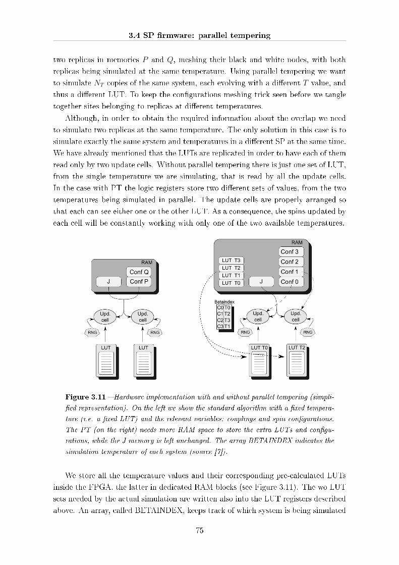
3.4 SP �rmware: parallel tempering
two replicas in memories P and Q, meshing their black and white nodes, with both
replicas being simulated at the same temperature. Using parallel tempering we want
to simulate NT copies of the same system, each evolving with a di�erent T value, and
thus a di�erent LUT. To keep the con�gurations meshing trick seen before we tangle
together sites belonging to replicas at di�erent temperatures.
Although, in order to obtain the required information about the overlap we need
to simulate two replicas at the same temperature. The only solution in this case is to
simulate exactly the same system and temperatures in a di�erent SP at the same time.
We have already mentioned that the LUTs are replicated in order to have each of them
read only by two update cells. Without parallel tempering there is just one set of LUT,
from the single temperature we are simulating, that is read by all the update cells.
In the case with PT the logic registers store two di�erent sets of values, from the two
temperatures being simulated in parallel. The update cells are properly arranged so
that each can see either one or the other LUT. As a consequence, the spins updated by
each cell will be constantly working with only one of the two available temperatures.
Figure 3.11 � Hardware implementation with and without parallel tempering (simpli-
�ed representation). On the left we show the standard algorithm with a �xed tempera-
ture (i.e. a �xed LUT) and the relevant variables: couplings and spin con�gurations.
The PT (on the right) needs more RAM space to store the extra LUTs and con�gu-
rations, while the J memory is left unchanged. The array BETAINDEX indicates the
simulation temperature of each system (source [7]).
We store all the temperature values and their corresponding pre-calculated LUTs
inside the FPGA, the latter in dedicated RAM blocks (see Figure 3.11). The wo LUT
sets needed by the actual simulation are written also into the LUT registers described
above. An array, called BETAINDEX, keeps track of which system is being simulated
75

Chapter 3. Janus architecture at large
at each temperature. When two con�gurations have been completely updated we move
to another pair of systems, once again each characterized by a (di�erent) temperature
value. The BETAINDEX values of the con�gurations that we are going to study point
to the memory location where the corresponding LUT values are stored. Once these
have been loaded into the LUT register we are ready to simulate the two new copies
of the system.
The PT algorithm requires some new functions (and consequently new hardware
blocks) as well. The �rst addition is related to the calculation (and storing) of the
energy value of each con�guration, necessary for the parallel tempering comparisons
(see equation 2.2.20). This is done by simply running the update algorithm over each
replica, but without actually updating the spin values in memories. Calculating the
energy of a whole lattice takes exactly the same time as updating the same lattice.
Once the energies of all con�gurations has been calculated, the values are used by the
PT for the comparisons.
The other important feature is the calculation of the logarithms of random numbers.
The PT algorithm works by comparing a random value with an exponential, namely
accepting the temperature swap when:
r 6 e∆β∆E with r ∈ [0; 1[ . (3.4.1)
In this case we cannot resort to the LUT trick used for the MC updates, since it
would be impossible to pre-calculate all the values of E. On the other hand, calcu-
lating the exponential value during the simulation would dramatically slow down the
performances of the machine. Our best choice is thus to use the alternative equation
ln r 6 ∆β∆E with r ∈ [0; 1[ (3.4.2)
exchanging the exponential function for a logarithm [8]. The logarithm operation is
rather slow as well, but we don't need to wait until the simulations are over to start
calculating it: since we need logarithms of random values we can generate these while
the simulations are still running.
When the MC steps of all the systems have been completed, we just have to evaluate
the products E and compare them with the pre-calculated ln r to decide whether to
accept or reject the parallel tempering switch. If this is accepted we exchange the
index values within the BETAINDEX array and move to the next pair of neighboring
temperatures. Once all the temperature pairs have been evaluated we are ready to
start again with the simulations, with each con�guration working at a newly-assigned
(hopefully reshu�ed) temperature.
The PT implementation described in this section is the best choice, for small lattice
sizes, because it is self-contained (within a single SP) and doesn't need too much time-
wasting communications. On the other hand, due to limited FPGA memory resources,
76

3.5 SP �rmware: graph coloring
this implementation works only with smaller lattice sizes (L 6 32) and a limited
number of temperatures (NT 6 128). For larger simulations with more temperatures
it is necessary to change the approach and work with more SPs, but it is not yet
implemented in Janus.
3.5 SP �rmware: graph coloring
The key point of the hardware implementation of the algorithm for graph coloring
is mapping of graph informations (color of each vertex and set of edges) within the
FPGA memories. The update process performed for each vertex is similar to the case
of the spin systems: the Metropolis algorithm is in fact the same. The challenge is
extracting parallelism from from an irregular and unpredictable structure such as a
random graph in order to perform parallel update of some nodes. Figure 3.12 shows a
small example of random graph.
3.5.1 Memory organization
In the case of spin glasses the trick of the bipartite lattice (see Figure 2.6) allows to
update whole set of the spin labelled as white in a single step and then all the black
ones. As random graph is characterized by a non-�xed connectivity, is not possible to
know in advance the number of edges for each vertex (that is equivalent to say that is
not possible to know how many neighbours have each spin in an hypothetic irregular
spin system).
Figure 3.12 � Example of a small random graph. Detailed balance of the Monte
Carlo requires that the state of the neighbour vertices should not change during the
update of a given vertex. In this �gure therefore is possible to update in parallel for
instance vertices 2, 3, 4, 5, 6, but not 1, 2, 3, 4, 5.
The �rst idea is therefore to process the graph structure that we plan to study
in order to �nd his degree of parallelism, i.e. we pre-process the input graph via a
77
Chapter 3. Janus architecture at large
standard PC. This �rst step is performed to obtain a partition of the vertices in k
subsets, Sk, each one containing p non adjacent vertices so that the number of vertices
|V | = k ·p. This rearrangement of the graph assures that each vertex of a set Si has no
neighbours in the same set Si and allows therefore the parallel update of all vertices
of the vertices in Si. This satis�es the detailed balance required by the Monte Carlo
Metropolis algorithm. It is important to note that this operation is in principle not
trivial (and not fast) when the average connectivity grows.
Any way after this preliminary operation we can suppose to have a graph in which
is possible to update in parallel k vertices. The second challenge is represented by the
mapping of graph structure within the memories of the FPGA. The only constraint is
now given my the fact that we want update k vertices at the same time, so we would
access informations related to the k updating vertices as fast as possible. It is clear
that considering V , set of vertices of a given graph, and Ni, set of neighbours of the
i-esim vertex, if we store informations by row in the form {Vi, Nij} with 0 6 i < |V |,0 6 j < |Ni| we obtain two disadvantages: i) we cannot know in advance width of
the table in which we plan to store graph information (or, in the case of the FPGA,
we cannot give a �xed dimension to a set of memories storing graph informations); ii)
technological limitations connected with FPGA do not allow to access more than two
locations per clock cycle and therefore, with this data organization we cannot take
advantage from the previous parallelism extraction.
Considering to store graph data by columns is possible to take advantage from
the rearrangement performed before. Each vertex has its own adjacency list stored
below itself so that column i contains {Vi, Nij}. Placing such structures one by one
in a row we obtain a set of b blocks, b = int{|V |/k}+ 1, each composed by a variable
number of rows and each row with k elements. First row of the block b0 contains �rst
k vertices, V0, ..., Vk−1 and following g rows the adjacency list ordered by columns,
with g = max{|Ni|, 0 6 i 6 k − 1}; second block b1 start on row g + 1 and contains
Vk, ..., V2k−1 followed by g rows, with g = max{|Ni|, k 6 i 6 2k − 1}, and so on.
In other words for each b so that 0 6 b 6 |V |/k + 1 we calculate
g(b) = max{|Ni| ; bk 6 i 6 k(b+ 1)− 1}.
First row of block b is:
{Vi ; kb 6 i 6 k(b+ 1)− 1}
following lines of block b are:
{Nij ; kb 6 i 6 k(b+ 1)− 1 ; 0 6 j 6 g(b)− 1}
In case that Vi has no neighbours in a given position ij we assume to store a dummy
word that is ignored by update engine. Blocks are stored one below the other and
last row of a block contains a �ag indicating the end of a block. We call this memory
78
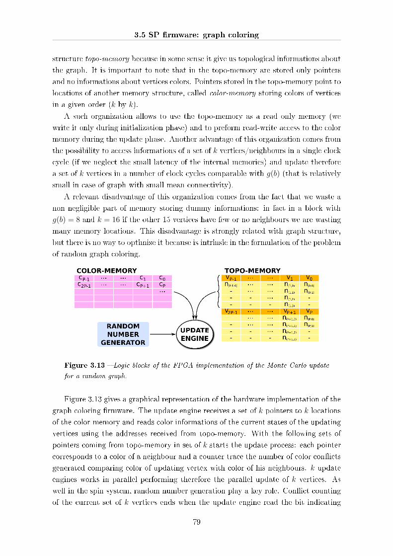
3.5 SP �rmware: graph coloring
structure topo-memory because in some sense it give us topological informations about
the graph. It is important to note that in the topo-memory are stored only pointers
and no informations about vertices colors. Pointers stored in the topo-memory point to
locations of another memory structure, called color-memory storing colors of vertices
in a given order (k by k).
A such organization allows to use the topo-memory as a read only memory (we
write it only during initialization phase) and to preform read-write access to the color
memory during the update phase. Another advantage of this organization comes from
the possibility to access informations of a set of k vertices/neighbours in a single clock
cycle (if we neglect the small latency of the internal memories) and update therefore
a set of k vertices in a number of clock cycles comparable with g(b) (that is relatively
small in case of graph with small mean connectivity).
A relevant disadvantage of this organization comes from the fact that we waste a
non negligible part of memory storing dummy informations: in fact in a block with
g(b) = 8 and k = 16 if the other 15 vertices have few or no neighbours we are wasting
many memory locations. This disadvantage is strongly related with graph structure,
but there is no way to optimize it because is intrinsic in the formulation of the problem
of random graph coloring.
Figure 3.13 � Logic blocks of the FPGA implementation of the Monte Carlo update
for a random graph.
Figure 3.13 gives a graphical representation of the hardware implementation of the
graph coloring �rmware. The update engine receives a set of k pointers to k locations
of the color-memory and reads color informations of the current states of the updating
vertices using the addresses received from topo-memory. With the following sets of
pointers coming from topo-memory in set of k starts the update process: each pointer
corresponds to a color of a neighbour and a counter trace the number of color con�icts
generated comparing color of updating vertex with color of his neighbours. k update
engines works in parallel performing therefore the parallel update of k vertices. As
well in the spin system, random number generation play a key role. Con�ict counting
of the current set of k vertices ends when the update engine read the bit indicating
79
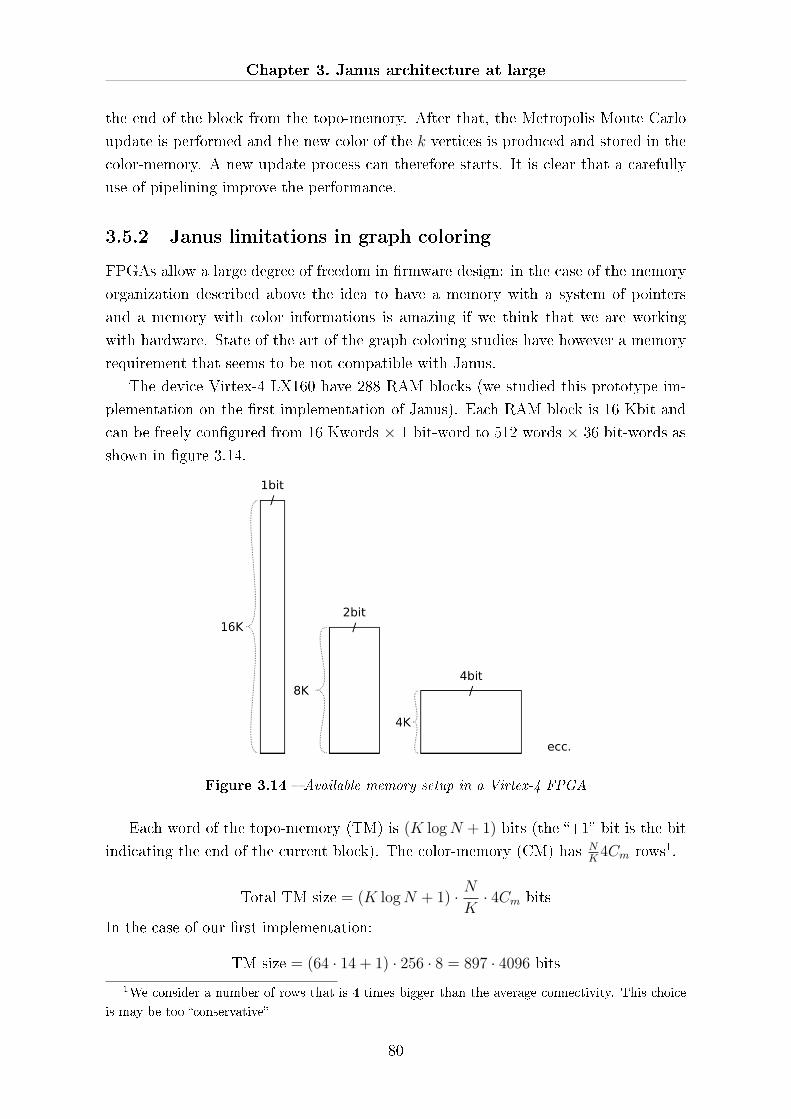
Chapter 3. Janus architecture at large
the end of the block from the topo-memory. After that, the Metropolis Monte Carlo
update is performed and the new color of the k vertices is produced and stored in the
color-memory. A new update process can therefore starts. It is clear that a carefully
use of pipelining improve the performance.
3.5.2 Janus limitations in graph coloring
FPGAs allow a large degree of freedom in �rmware design: in the case of the memory
organization described above the idea to have a memory with a system of pointers
and a memory with color informations is amazing if we think that we are working
with hardware. State of the art of the graph coloring studies have however a memory
requirement that seems to be not compatible with Janus.
The device Virtex-4 LX160 have 288 RAM blocks (we studied this prototype im-
plementation on the �rst implementation of Janus). Each RAM block is 16 Kbit and
can be freely con�gured from 16 Kwords × 1 bit-word to 512 words × 36 bit-words as
shown in �gure 3.14.
Figure 3.14 � Available memory setup in a Virtex-4 FPGA
Each word of the topo-memory (TM) is (K logN + 1) bits (the �+1� bit is the bit
indicating the end of the current block). The color-memory (CM) has NK
4Cm rows1.
Total TM size = (K logN + 1) · NK· 4Cm bits
In the case of our �rst implementation:
TM size = (64 · 14 + 1) · 256 · 8 = 897 · 4096 bits
1We consider a number of rows that is 4 times bigger than the average connectivity. This choice
is may be too �conservative�
80

3.5 SP �rmware: graph coloring
Using the Xilinx memory, we need 225 blocks with the con�guration 4K words ×4 bit-word to build the topo-memory.
Each word of the color-memory use K · logB bits (with logB the number of bits
used to represent a color). The CM has NKrows and will be replicate K
2times in order
to access k vertices data in a single clock cycle (using the dual port con�guration).
Total CM size = K · logB · NK· K
2=K
2· logB ·N bits
In our implementation:
CM size = 32 · 2 · 214 = 32 · 32.768 bits
Using the Xilinx memory, we need 4 blocks with the con�guration 512 words × 36
bit-word to build the CM, but we need to replicate the CM structure K/2 times, i.e.
we need 4 · 32 Xilinx RAM blocks to build the complete CM parallel system.
From this very preliminary study we have two conclusions:
1. the total number of bits for the TM and the CM is:
(897 · 4096) + (32 · 32.768) = 3.674.112 + 1.048.576 = 4.722.688
This number is smaller than the total available bits in a Virtex-4 LX160.
2. the total number of blocks needed for TM and CM is: 225 + 128 = 353
This number is bigger than the total number of blocks available in a Virtex-4
LX160.
Balancing of 1 and 2 were the optimum solution, but seems to be di�cult to reach
with the present realization of Janus: embedded memory are in fact the limiting factor
for a more e�cient implementation.
Moreover the state of the art of random graph studies requires to be able to ap-
proach graphs of more than 50000 vertices, that is far to the present realization with
Janus.
81


Bibliography
[1] S. Sumimoto et al., The design and evaluation of high performance communication
using a Gigabit Ethernet, proceedings of the 13th international conference on
Supercomputing, 260 (1999). 3.2.3
[2] F. Belletti et al., Computing for LQCD: apeNEXT, Computing in Science &
Engineering, vol. 8, pp. 18-29, (2006). 3.2.6
[3] R. Baxter et al., Maxwell a 64 FPGA Supercomputer, Proceedings AHS2007 Con-
ference Second NASA/ESA Conference on Adaptive Hardware andSystems, Ed-
inburgh, (2007).
http://www.fhpca.org/download/RSSI07-Maxwell.pdf 3.2.6
[4] F. Belletti et al., Ianus: an Adpative FPGA Computer, Computing in Science &
Engineering vol. 8, pp. 41-49 (2006). 3.2.6, 3.3.2
[5] F. Belletti et al., Janus: a Cost E�cient FPGA-Based Monte Carlo Simu-
lation Engine, technical report http://df.unife.it/janus/papers/gbpaper_
sub2.pdf. 3.2.6
[6] D. P. Landau and K. Binder, A Guide to Monte Carlo Simulations in Statistical
Physics, Cambridge University Press (2005). 3.3.1
[7] D. Sciretti, Spin Glasses, Protein Design and Dedicated Computers, PhD thesis,
Instituto de Biocomputación y Física de Sistemas Complejos (2008). 3.11
[8] J. Detrey and F. de Dinechin, Microprocessors and Microsystems 31 (8), 537
(2007). 3.4
83

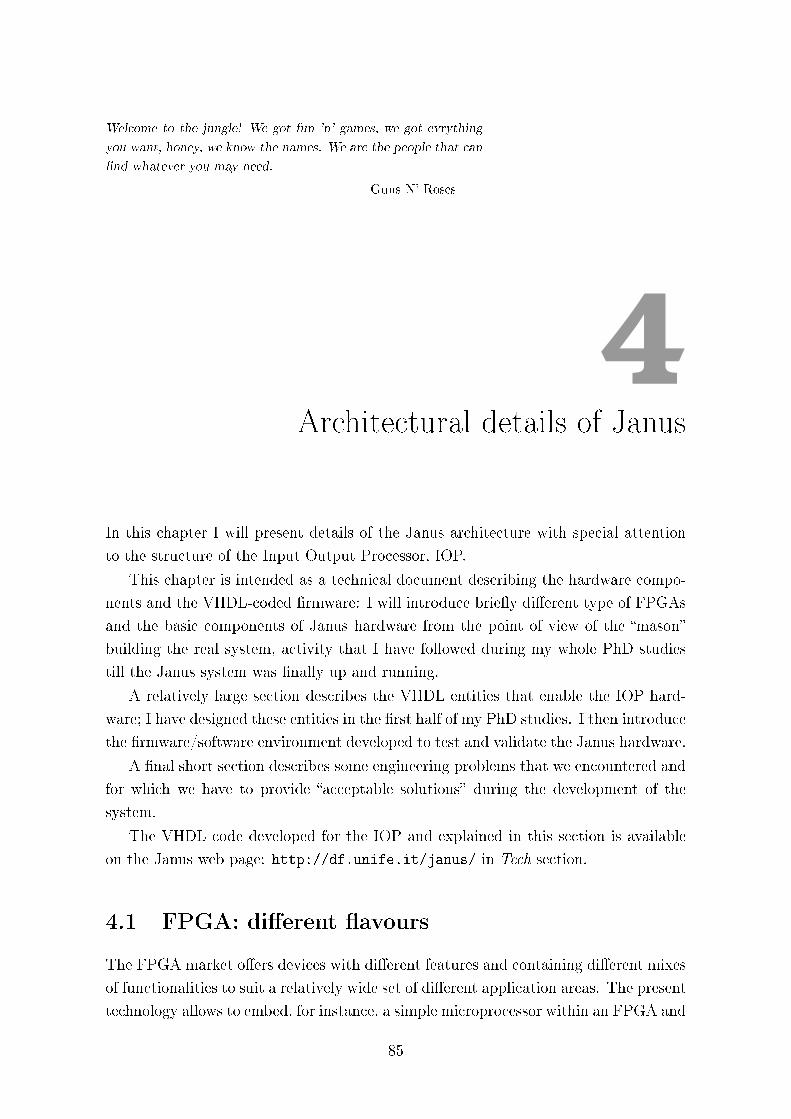
Welcome to the jungle! We got fun 'n' games, we got evrything
you want, honey, we know the names. We are the people that can
�nd whatever you may need.
Guns N' Roses
4Architectural details of Janus
In this chapter I will present details of the Janus architecture with special attention
to the structure of the Input Output Processor, IOP.
This chapter is intended as a technical document describing the hardware compo-
nents and the VHDL-coded �rmware: I will introduce brie�y di�erent type of FPGAs
and the basic components of Janus hardware from the point of view of the �mason�
building the real system, activity that I have followed during my whole PhD studies
till the Janus system was �nally up and running.
A relatively large section describes the VHDL entities that enable the IOP hard-
ware; I have designed these entities in the �rst half of my PhD studies. I then introduce
the �rmware/software environment developed to test and validate the Janus hardware.
A �nal short section describes some engineering problems that we encountered and
for which we have to provide �acceptable solutions� during the development of the
system.
The VHDL code developed for the IOP and explained in this section is available
on the Janus web page: http://df.unife.it/janus/ in Tech section.
4.1 FPGA: di�erent �avours
The FPGA market o�ers devices with di�erent features and containing di�erent mixes
of functionalities to suit a relatively wide set of di�erent application areas. The present
technology allows to embed, for instance, a simple microprocessor within an FPGA and
85
Chapter 4. Architectural details of Janus
have therefore a chip including a general purpose processor able to run an operating
system and, at the same time, a non negligible quantity of con�gurable logic Other
devices, optimized for high speed communications, embed for instance several (at
present 8 to 20) high speed interfaces (e.g. PCI or Gigabit hard-cores). Other FPGAs
o�ers a huge quantity of embedded memory.
The FPGA panorama is therefore various and the choice of a device for Janus was
driven by the simple idea that the only important feature is the availability of memory
and logic elements in order to store lattices as large as possible and to house the highest
number of update engines. Large on chip memory size and many logic elements are
obviously con�icting requirements; each FPGA family o�ers di�erent trade o�s.
Our preliminary prototype was developed in 2005 using a PCI development kit [1]
housing an Altera Stratix S60 FPGA, containing ∼ 57000 logic elements and ∼ 5 MB
of embedded memory1.
Figure 4.1 � Table summarizing main features of Xilinx Virtex-4 FPGA family
(source [2]).
The �rst two Janus prototype boards developed in 2006 had Xilinx Virtex-4 LX160
FPGA while the �nal realization of the system was based on Xilinx Virtex-4 LX200.
Figure 4.1 summarizes the main features of Xilinx Virtex-4 FPGA, that are divided
in three main families: LX, optimized for logic and memories; SX, housing a huge
1Altera Stratix I devices embed memories organized in three di�erent size: 574 blocks, calledM512
RAM, that can be con�gured up to 32 × 18 bits, 292 blocks, called M4K RAM, con�gurable up to
128× 36 bits and 6 blocks, called M-RAM, con�gurable up to 4K × 144 bits.
86
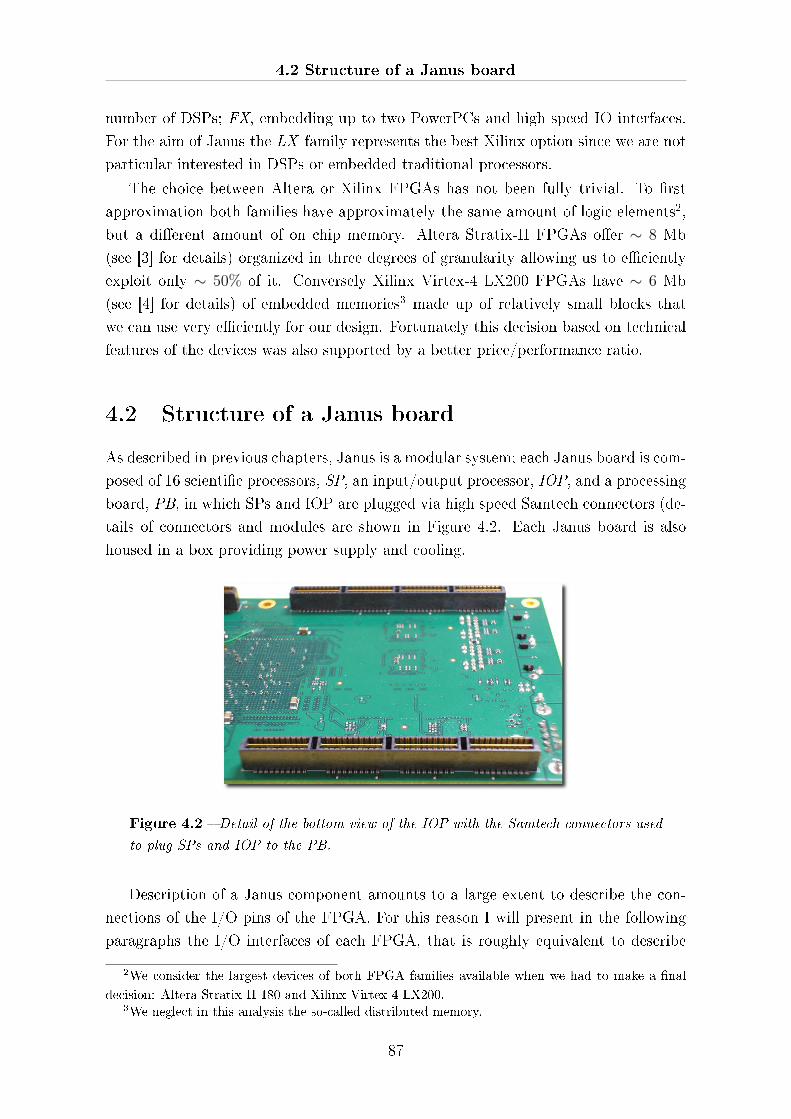
4.2 Structure of a Janus board
number of DSPs; FX, embedding up to two PowerPCs and high speed IO interfaces.
For the aim of Janus the LX family represents the best Xilinx option since we are not
particular interested in DSPs or embedded traditional processors.
The choice between Altera or Xilinx FPGAs has not been fully trivial. To �rst
approximation both families have approximately the same amount of logic elements2,
but a di�erent amount of on chip memory. Altera Stratix-II FPGAs o�er ∼ 8 Mb
(see [3] for details) organized in three degrees of granularity allowing us to e�ciently
exploit only ∼ 50% of it. Conversely Xilinx Virtex-4 LX200 FPGAs have ∼ 6 Mb
(see [4] for details) of embedded memories3 made up of relatively small blocks that
we can use very e�ciently for our design. Fortunately this decision based on technical
features of the devices was also supported by a better price/performance ratio.
4.2 Structure of a Janus board
As described in previous chapters, Janus is a modular system; each Janus board is com-
posed of 16 scienti�c processors, SP, an input/output processor, IOP, and a processing
board, PB, in which SPs and IOP are plugged via high speed Samtech connectors (de-
tails of connectors and modules are shown in Figure 4.2. Each Janus board is also
housed in a box providing power supply and cooling.
Figure 4.2 � Detail of the bottom view of the IOP with the Samtech connectors used
to plug SPs and IOP to the PB.
Description of a Janus component amounts to a large extent to describe the con-
nections of the I/O pins of the FPGA. For this reason I will present in the following
paragraphs the I/O interfaces of each FPGA, that is roughly equivalent to describe
2We consider the largest devices of both FPGA families available when we had to make a �nal
decision: Altera Stratix-II 180 and Xilinx Virtex-4 LX200.3We neglect in this analysis the so-called distributed memory.
87
Chapter 4. Architectural details of Janus
the structure of a Janus board apart for the power supply system. A paragraph is also
dedicated to the description of the Janus box.
4.2.1 SP
All SPs are directly connected in a mesh (i.e. each board represents a nearest neigh-
bours network with toroidal enclosure) on a 16 lines full duplex di�erential bus (16
di�erential input lines + 16 di�erential output lines). Moreover each SP has a private
single ended full duplex link with the IOP composed of 10 lines.
Other single ended lines reaching the SP from the PB via connectors are:
clock: 2 input clock lines. A common clock frequency is generated by an oscil-
lator on the PB and distributed to all modules; 2 additional FPGA I/O
pins are available for feedback for each input clock; FPGA pins in close
proximity of the clock signals are not used to reduce noise.
syncIn: 4 input lines used by FPGA �rmware for synchronization (the same set
of synchronization signals is shared by 4 SPs).
syncOut: 4 output lines used by FPGA �rmware to send synchronization messages
to the IOP (synchronization signals from SPs to IOP are point to point).
progLine: 21 lines driven by the IOP programming interface in order to con�gure
each SP as needed; we use the select map con�guration mode that re-
quires 8 bits data bus connected with 8 FPGA I/O pins and 13 lines
connected to an equal number of dedicated FPGA pins driving the con-
�guration.
spReset: 2 input lines coding various level of resets.
The rest of the pins used for input/output are dedicated to test points (16 pins),
temperature sensor lying on each daughter card (3 I/O pins + 2 dedicated pins) and
reset button (1 pin). These lines are however on board signals and have no connections
with the PB. Four more dedicated on board pins are used for JTAG con�guration that
we used only during the prototype phase and for hardware debug via Chipscope [5].
More details about con�guration are explained in 4.3.5 and in [6].
The total number of input/output pins4 for the FPGA of each SP are therefore
312, equivalent to ∼ 33% of the I/O pins available. Table 4.1 summarizes pins usage
in an SP module (neglecting power and ground pins).
Part of the SP area houses the 2.5 V to 1.2 V DCDC power modules. This last
stage of power conversion su�ered from several engineering problems, as, in the early
4Exact number calculated in view of the entries of the user con�guration �le UCF used by the
synthesis tool.
88

4.2 Structure of a Janus board
Logical function Pin # & type Direction
Link to SP
North, South, East, West4× 16 LVDS pairs Output
Link from SP
North, South, East, West4× 16 LVDS pairs Input
Link to IOP 10 LVCMOS Output
Link from IOP 10 LVCMOS Input
Sync to IOP 4 LVCMOS Output
Sync from IOP 4 LVCMOS Input
Test points 16 LVCMOS Output
Clock 6 LVCMOS4 Input
2 Output
Reset 3 LVCMOS Input
Temperature sensor3 LVCMOS
2 dedicated pins
2 InOut + 1 Input
-
JTAG 4 dedicated pins -
Con�guration channels 21 dedicated pins -
Table 4.1 � Pin assignment summary of the SP module.
design phases, we severely underestimated the power needed by our FPGAs. These
problems (and how we solved it) are described in details in Section 4.5).
4.2.2 IOP
The hardware design of IOP is more complex then the SP because this daughter
card performs numerous and various tasks and therefore houses a higher number of
components. Looking at the connectors with the PB, the presence of a 10 bit bus per
direction for each SP requires that a huge number of lines reach the PB.
Components on board are: 2 Gigabit PHYs (model Marvell 88E1111), 1 UART in-
terface chip (model Maxim MAX3381E), 1 USB-bridge (model CP2102), 2 EEPROMs
for FPGA con�guration on boot up (model XCF32PVOG48C), 2 staging memories
(model NEC µPD44321361), 1 temperature sensor (model MAX1617A), 2 JTAG inter-
faces, 1 oscillator generating the clock for Gigabit PHYs, 1 LEMO connector to accept
external clock and 1 reset button. Figure 4.3 shows an the IOP complete schematic
design with its main components.
Pin assignment of the IOP FPGA can be summarized as follows:
- 105 pins dedicated to staging memory: 64 pins for data, 20 pins for address, 2
pins for clocks, 8 pins for parity, 1 pin for write enable and 10 pins for controls.
89
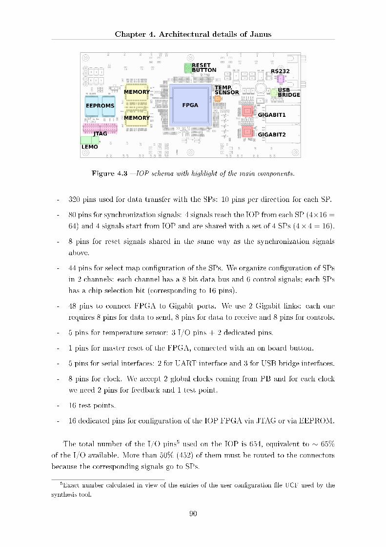
Chapter 4. Architectural details of Janus
Figure 4.3 � IOP schema with highlight of the main components.
- 320 pins used for data transfer with the SPs: 10 pins per direction for each SP.
- 80 pins for synchronization signals: 4 signals reach the IOP from each SP (4×16 =
64) and 4 signals start from IOP and are shared with a set of 4 SPs (4× 4 = 16).
- 8 pins for reset signals shared in the same way as the synchronization signals
above.
- 44 pins for select map con�guration of the SPs. We organize con�guration of SPs
in 2 channels: each channel has a 8 bit data bus and 6 control signals; each SPs
has a chip selection bit (corresponding to 16 pins).
- 48 pins to connect FPGA to Gigabit ports. We use 2 Gigabit links: each one
requires 8 pins for data to send, 8 pins for data to receive and 8 pins for controls.
- 5 pins for temperature sensor: 3 I/O pins + 2 dedicated pins.
- 1 pins for master reset of the FPGA, connected with an on board button.
- 5 pins for serial interfaces: 2 for UART interface and 3 for USB bridge interfaces.
- 8 pins for clock. We accept 2 global clocks coming from PB and for each clock
we need 2 pins for feedback and 1 test point.
- 16 test points.
- 16 dedicated pins for con�guration of the IOP FPGA via JTAG or via EEPROM.
The total number of the I/O pins5 used on the IOP is 654, equivalent to ∼ 65%
of the I/O available. More than 50% (452) of them must be routed to the connectors
because the corresponding signals go to SPs.
5Exact number calculated in view of the entries of the user con�guration �le UCF used by the
synthesis tool.
90
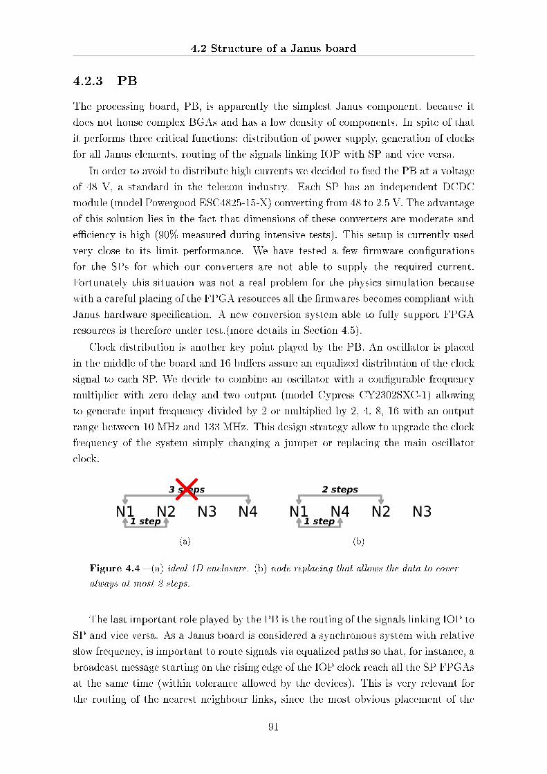
4.2 Structure of a Janus board
4.2.3 PB
The processing board, PB, is apparently the simplest Janus component, because it
does not house complex BGAs and has a low density of components. In spite of that
it performs three critical functions: distribution of power supply, generation of clocks
for all Janus elements, routing of the signals linking IOP with SP and vice versa.
In order to avoid to distribute high currents we decided to feed the PB at a voltage
of 48 V, a standard in the telecom industry. Each SP has an independent DCDC
module (model Powergood ESC4825-15-X) converting from 48 to 2.5 V. The advantage
of this solution lies in the fact that dimensions of these converters are moderate and
e�ciency is high (90% measured during intensive tests). This setup is currently used
very close to its limit performance. We have tested a few �rmware con�gurations
for the SPs for which our converters are not able to supply the required current.
Fortunately this situation was not a real problem for the physics simulation because
with a careful placing of the FPGA resources all the �rmwares becomes compliant with
Janus hardware speci�cation. A new conversion system able to fully support FPGA
resources is therefore under test.(more details in Section 4.5).
Clock distribution is another key point played by the PB. An oscillator is placed
in the middle of the board and 16 bu�ers assure an equalized distribution of the clock
signal to each SP. We decide to combine an oscillator with a con�gurable frequency
multiplier with zero delay and two output (model Cypress CY2302SXC-1) allowing
to generate input frequency divided by 2 or multiplied by 2, 4, 8, 16 with an output
range between 10 MHz and 133 MHz. This design strategy allow to upgrade the clock
frequency of the system simply changing a jumper or replacing the main oscillator
clock.
(a) (b)
Figure 4.4 � (a) ideal 1D enclosure. (b) node replacing that allows the data to cover
always at most 2 steps.
The last important role played by the PB is the routing of the signals linking IOP to
SP and vice versa. As a Janus board is considered a synchronous system with relative
slow frequency, is important to route signals via equalized paths so that, for instance, a
broadcast message starting on the rising edge of the IOP clock reach all the SP FPGAs
at the same time (within tolerance allowed by the devices). This is very relevant for
the routing of the nearest neighbour links, since the most obvious placement of the
91

Chapter 4. Architectural details of Janus
SPs would imply physical paths for the links of widely di�erent lengths as explained
in 1D by Figure 4.4a. We can go around this problem with a simple change in the
placement of the nodes, as shown in Figure 4.4b.
Following this idea the actual position of the SPs in a Janus board are not as in
Figure 4.5a but as in Figure 4.5b6.
(a) (b)
Figure 4.5 � Each SP is represented by a pair of numbers representing the Cartesian
coordinates of the SP in a XY -plane. (a) Cartesian placement of a toroidal mesh.
(b) Placement of the SPs in a Janus board, partially equalizing the length of the paths
between nearest neighbours.
4.2.4 Janus box
Each board is housed in a case providing power supply, plugs connecting to the host
PC and a complex fan system needed remove heat and keep temperature within a
reasonable working range.
Connectors are placed on the back panel of the box and are arranged as shown in
Figure 4.6a. There is a power plug and a power switch and the following interfaces:
two Gigabit plugs, one USB and one RS232 connector and two JTAG interfaces. In the
present system setup only one Gigabit plug and optionally the serial line for debug are
connected. Two JTAG interfaces are available in order to recon�gure independently
the IOP FPGA or the EEPROM placed on the IOP.
Our cooling system is provided by static heat sink of di�erent height placed on
the FPGAs and a system of ten fans arranged in three lines: four at the front, four
in the middle and two on back panel so air �ows from the front to the back. Heat
sinks are placed so that the 4 FPGAs near the front panel, where air has the lowest
6Note that the Y axis does not respect exactly the rules minimizing the path described in previous
paragraph: the reason of that is related with the problems of routing of the signals within the PB.
92
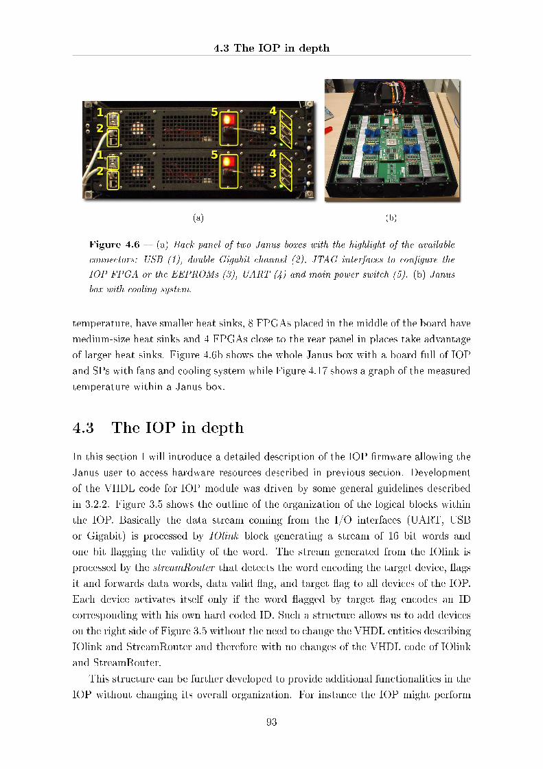
4.3 The IOP in depth
(a) (b)
Figure 4.6 � (a) Back panel of two Janus boxes with the highlight of the available
connectors: USB (1), double Gigabit channel (2), JTAG interfaces to con�gure the
IOP FPGA or the EEPROMs (3), UART (4) and main power switch (5). (b) Janus
box with cooling system.
temperature, have smaller heat sinks, 8 FPGAs placed in the middle of the board have
medium-size heat sinks and 4 FPGAs close to the rear panel in places take advantage
of larger heat sinks. Figure 4.6b shows the whole Janus box with a board full of IOP
and SPs with fans and cooling system while Figure 4.17 shows a graph of the measured
temperature within a Janus box.
4.3 The IOP in depth
In this section I will introduce a detailed description of the IOP �rmware allowing the
Janus user to access hardware resources described in previous section. Development
of the VHDL code for IOP module was driven by some general guidelines described
in 3.2.2. Figure 3.5 shows the outline of the organization of the logical blocks within
the IOP. Basically the data stream coming from the I/O interfaces (UART, USB
or Gigabit) is processed by IOlink block generating a stream of 16 bit words and
one bit �agging the validity of the word. The stream generated from the IOlink is
processed by the streamRouter that detects the word encoding the target device, �ags
it and forwards data words, data valid �ag, and target �ag to all devices of the IOP.
Each device activates itself only if the word �agged by target �ag encodes an ID
corresponding with his own hard coded ID. Such a structure allows us to add devices
on the right side of Figure 3.5 without the need to change the VHDL entities describing
IOlink and StreamRouter and therefore with no changes of the VHDL code of IOlink
and StreamRouter.
This structure can be further developed to provide additional functionalities in the
IOP without changing its overall organization. For instance the IOP might perform
93
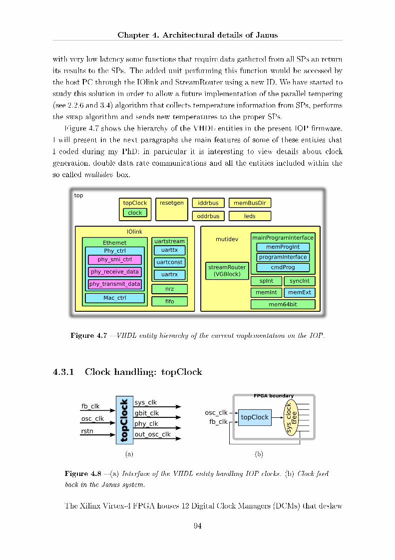
Chapter 4. Architectural details of Janus
with very low latency some functions that require data gathered from all SPs an return
its results to the SPs. The added unit performing this function would be accessed by
the host PC through the IOlink and StreamRouter using a new ID. We have started to
study this solution in order to allow a future implementation of the parallel tempering
(see 2.2.6 and 3.4) algorithm that collects temperature information from SPs, performs
the swap algorithm and sends new temperatures to the proper SPs.
Figure 4.7 shows the hierarchy of the VHDL entities in the present IOP �rmware.
I will present in the next paragraphs the main features of some of these entities that
I coded during my PhD: in particular it is interesting to view details about clock
generation, double data rate communications and all the entities included within the
so called multidev box.
Figure 4.7 � VHDL entity hierarchy of the current implementation on the IOP.
4.3.1 Clock handling: topClock
(a) (b)
Figure 4.8 � (a) Interface of the VHDL entity handling IOP clocks. (b) Clock feed-
back in the Janus system.
The Xilinx Virtex-4 FPGA houses 12 Digital Clock Managers (DCMs) that deskew
94
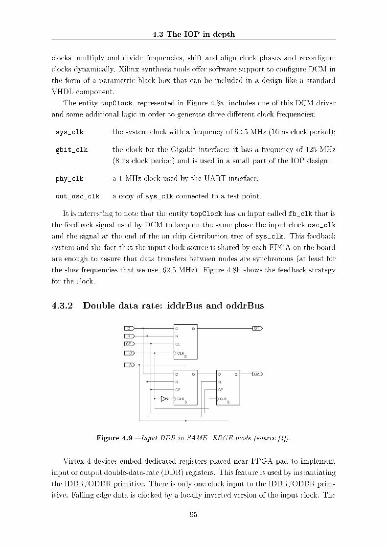
4.3 The IOP in depth
clocks, multiply and divide frequencies, shift and align clock phases and recon�gure
clocks dynamically. Xilinx synthesis tools o�er software support to con�gure DCM in
the form of a parametric black box that can be included in a design like a standard
VHDL component.
The entity topClock, represented in Figure 4.8a, includes one of this DCM driver
and some additional logic in order to generate three di�erent clock frequencies:
sys_clk the system clock with a frequency of 62.5 MHz (16 ns clock period);
gbit_clk the clock for the Gigabit interface: it has a frequency of 125 MHz
(8 ns clock period) and is used in a small part of the IOP design;
phy_clk a 1 MHz clock used by the UART interface;
out_osc_clk a copy of sys_clk connected to a test point.
It is interesting to note that the entity topClock has an input called fb_clk that is
the feedback signal used by DCM to keep on the same phase the input clock osc_clk
and the signal at the end of the on chip distribution tree of sys_clk. This feedback
system and the fact that the input clock source is shared by each FPGA on the board
are enough to assure that data transfers between nodes are synchronous (at least for
the slow frequencies that we use, 62.5 MHz). Figure 4.8b shows the feedback strategy
for the clock.
4.3.2 Double data rate: iddrBus and oddrBus
Figure 4.9 � Input DDR in SAME_EDGE mode (source [4]).
Virtex-4 devices embed dedicated registers placed near FPGA pad to implement
input or output double-data-rate (DDR) registers. This feature is used by instantiating
the IDDR/ODDR primitive. There is only one clock input to the IDDR/ODDR prim-
itive. Falling edge data is clocked by a locally inverted version of the input clock. The
95

Chapter 4. Architectural details of Janus
IDDR/ODDR primitive supports di�erent modes of operation; we use SAME_EDGE
mode for both directions, input and output. Figure 4.9 shows, for instance, input
DDR registers and the signals associated with the SAME_EDGE mode. Figure 4.10
shows the timing diagram of the input DDR using the SAME_EDGE mode.
Figure 4.10 � Input DDR Timing in SAME_EDGE mode (source [4]).
The entities iddrBus and oddrBus are wrappers that instantiate respectively a set
of N IDDR or ODDR Xilinx black boxes in order to obtain a double-data-rate bus of N
bits. We use them in the links between IOP and SPs to double the bandwidth.
Implementation of this technology is useful, but it becomes less reliable when the
logic resource usage of the FPGA exceeds ∼ 85%. In this case in fact the duty cycle
of the system clock becomes appreciably asymmetric: the part of the design working
with rising edge of the clock works �ne because the DCM aligns phase looking at the
rising edge of the input clock and the feedback clock, but 50% duty cycle constraint is
not meet and logic using both edges, such as DDR I/O registers, becomes completely
unstable (see also 4.5).
4.3.3 Message routing: StreamRouter
StreamRouter is a key entity in the IOP architecture (its interface is shown in Fig-
ure 4.11a): all messages coming from IOlink pass trough it and are routed to destina-
tion device following an easy protocol, called encapsulated protocol.
We assume that each target device has a device ID bitwise coded in a 16 bit word,
called devSelMask. Each message starting from host PC (under the form of data
stream) must have an header composed of three words of 16 bits coding respectively:
word #1 → devSelMask coding target device;
word #2→ len #0 less signi�cant 16 bits of the length of the following message (unit
of measurement is 16 bit word);
word #3 → len #1 most signi�cant 16 bits of the length above.
Data following word #3 contains message for the target device. For a graphical repre-
sentation of a message see Figure 3.6 in previous chapter.
StreamRouter decodes information contained in the header, removes words coding
96
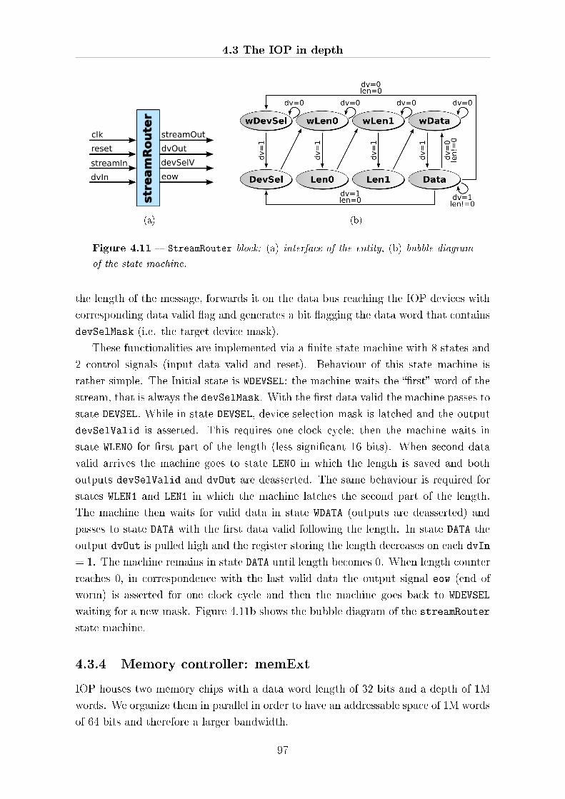
4.3 The IOP in depth
(a) (b)
Figure 4.11 � StreamRouter block: (a) interface of the entity, (b) bubble diagram
of the state machine.
the length of the message, forwards it on the data bus reaching the IOP devices with
corresponding data valid �ag and generates a bit �agging the data word that contains
devSelMask (i.e. the target device mask).
These functionalities are implemented via a �nite state machine with 8 states and
2 control signals (input data valid and reset). Behaviour of this state machine is
rather simple. The Initial state is WDEVSEL: the machine waits the ��rst� word of the
stream, that is always the devSelMask. With the �rst data valid the machine passes to
state DEVSEL. While in state DEVSEL, device selection mask is latched and the output
devSelValid is asserted. This requires one clock cycle; then the machine waits in
state WLEN0 for �rst part of the length (less signi�cant 16 bits). When second data
valid arrives the machine goes to state LEN0 in which the length is saved and both
outputs devSelValid and dvOut are deasserted. The same behaviour is required for
states WLEN1 and LEN1 in which the machine latches the second part of the length.
The machine then waits for valid data in state WDATA (outputs are deasserted) and
passes to state DATA with the �rst data valid following the length. In state DATA the
output dvOut is pulled high and the register storing the length decreases on each dvIn
= 1. The machine remains in state DATA until length becomes 0. When length counter
reaches 0, in correspondence with the last valid data the output signal eow (end of
worm) is asserted for one clock cycle and then the machine goes back to WDEVSEL
waiting for a new mask. Figure 4.11b shows the bubble diagram of the streamRouter
state machine.
4.3.4 Memory controller: memExt
IOP houses two memory chips with a data word length of 32 bits and a depth of 1M
words. We organize them in parallel in order to have an addressable space of 1M words
of 64 bits and therefore a larger bandwidth.
97
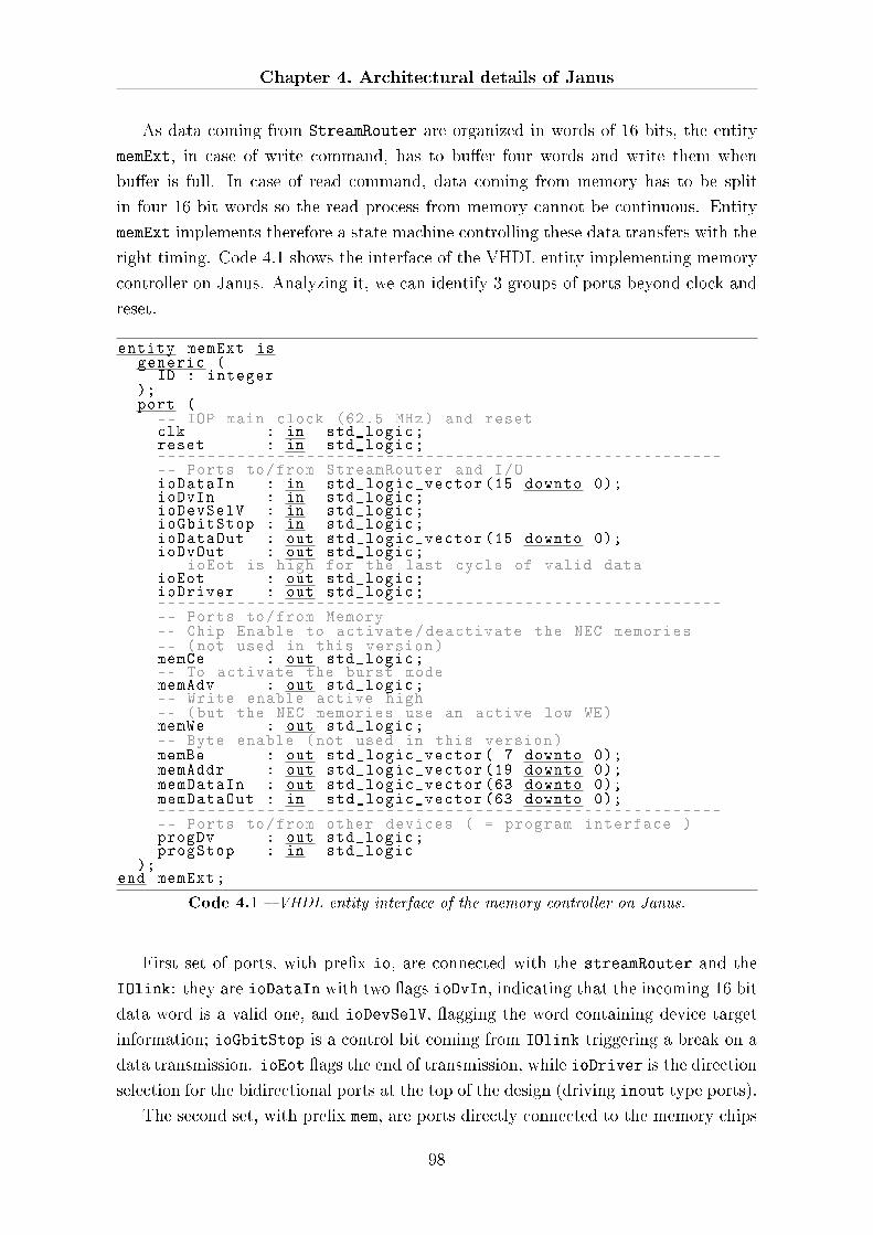
Chapter 4. Architectural details of Janus
As data coming from StreamRouter are organized in words of 16 bits, the entity
memExt, in case of write command, has to bu�er four words and write them when
bu�er is full. In case of read command, data coming from memory has to be split
in four 16 bit words so the read process from memory cannot be continuous. Entity
memExt implements therefore a state machine controlling these data transfers with the
right timing. Code 4.1 shows the interface of the VHDL entity implementing memory
controller on Janus. Analyzing it, we can identify 3 groups of ports beyond clock and
reset.
entity memExt isgeneric (
ID : integer);port (
-- IOP main clock (62.5 MHz) and resetclk : in std_logic;reset : in std_logic;----------------------------------------------------------- Ports to/from StreamRouter and I/OioDataIn : in std_logic_vector (15 downto 0);ioDvIn : in std_logic;ioDevSelV : in std_logic;ioGbitStop : in std_logic;ioDataOut : out std_logic_vector (15 downto 0);ioDvOut : out std_logic;-- ioEot is high for the last cycle of valid dataioEot : out std_logic;ioDriver : out std_logic;----------------------------------------------------------- Ports to/from Memory-- Chip Enable to activate/deactivate the NEC memories-- (not used in this version)memCe : out std_logic;-- To activate the burst modememAdv : out std_logic;-- Write enable active high-- (but the NEC memories use an active low WE)memWe : out std_logic;-- Byte enable (not used in this version)memBe : out std_logic_vector( 7 downto 0);memAddr : out std_logic_vector (19 downto 0);memDataIn : out std_logic_vector (63 downto 0);memDataOut : in std_logic_vector (63 downto 0);----------------------------------------------------------- Ports to/from other devices ( = program interface )progDv : out std_logic;progStop : in std_logic
);end memExt;
Code 4.1 � VHDL entity interface of the memory controller on Janus.
First set of ports, with pre�x io, are connected with the streamRouter and the
IOlink: they are ioDataIn with two �ags ioDvIn, indicating that the incoming 16 bit
data word is a valid one, and ioDevSelV, �agging the word containing device target
information; ioGbitStop is a control bit coming from IOlink triggering a break on a
data transmission. ioEot �ags the end of transmission, while ioDriver is the direction
selection for the bidirectional ports at the top of the design (driving inout type ports).
The second set, with pre�x mem, are ports directly connected to the memory chips
98
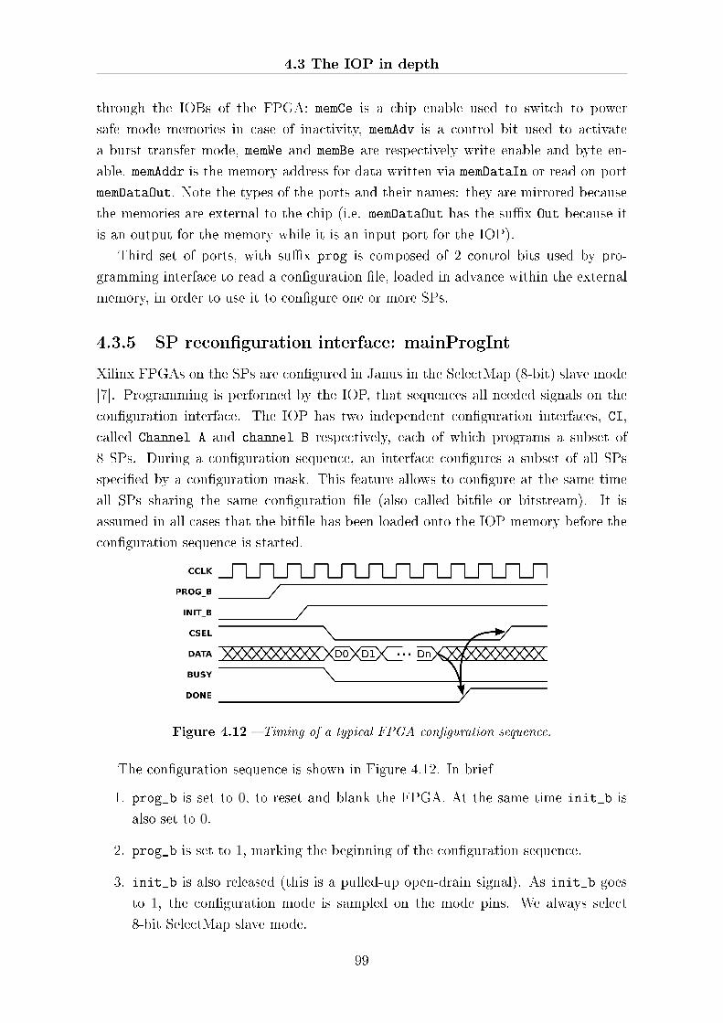
4.3 The IOP in depth
through the IOBs of the FPGA: memCe is a chip enable used to switch to power
safe mode memories in case of inactivity, memAdv is a control bit used to activate
a burst transfer mode, memWe and memBe are respectively write enable and byte en-
able. memAddr is the memory address for data written via memDataIn or read on port
memDataOut. Note the types of the ports and their names: they are mirrored because
the memories are external to the chip (i.e. memDataOut has the su�x Out because it
is an output for the memory while it is an input port for the IOP).
Third set of ports, with su�x prog is composed of 2 control bits used by pro-
gramming interface to read a con�guration �le, loaded in advance within the external
memory, in order to use it to con�gure one or more SPs.
4.3.5 SP recon�guration interface: mainProgInt
Xilinx FPGAs on the SPs are con�gured in Janus in the SelectMap (8-bit) slave mode
[7]. Programming is performed by the IOP, that sequences all needed signals on the
con�guration interface. The IOP has two independent con�guration interfaces, CI,
called Channel A and channel B respectively, each of which programs a subset of
8 SPs. During a con�guration sequence, an interface con�gures a subset of all SPs
speci�ed by a con�guration mask. This feature allows to con�gure at the same time
all SPs sharing the same con�guration �le (also called bit�le or bitstream). It is
assumed in all cases that the bit�le has been loaded onto the IOP memory before the
con�guration sequence is started.
Figure 4.12 � Timing of a typical FPGA con�guration sequence.
The con�guration sequence is shown in Figure 4.12. In brief
1. prog_b is set to 0, to reset and blank the FPGA. At the same time init_b is
also set to 0.
2. prog_b is set to 1, marking the beginning of the con�guration sequence.
3. init_b is also released (this is a pulled-up open-drain signal). As init_b goes
to 1, the con�guration mode is sampled on the mode pins. We always select
8-bit SelectMap slave mode.
99
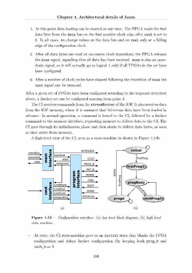
Chapter 4. Architectural details of Janus
4. At this point data loading can be started at any time. The FPGA reads the �rst
data byte from the data bus on the �rst positive clock edge after csel is set to
0. In all cases, we change values on the data bus and on csel only at a falling
edge of the con�guration clock.
5. After all data bytes are read on successive clock transitions, the FPGA releases
the done signal, signalling that all data has been received. done is also an open-
drain signal, so it will actually go to logical 1 only if all FPGAs in the set have
been con�gured.
6. After a number of clock cycles have elapsed following the transition of done the
csel signal can be removed.
After a given set of FPGAs have been con�gured according to the sequence described
above, a further set can be con�gured starting from point 4.
The CI receives commands from the streamRouter of the IOP. It also receives data
from the IOP memory, where it is assumed that bitstream data have been loaded in
advance. In normal operation, a command is issued to the CI, followed by a further
command to the memory interface, requesting memory to deliver data to the CI. The
CI goes through its initialization phase and then starts to deliver data bytes, as soon
as they arrive from memory.
A high-level view of the CI, seen as a state-machine in shown in Figure 4.13b.
(a) (b)
Figure 4.13 � Con�guration interface: (a) top level block diagram, (b) high level
state machine.
- At reset, the CI state-machine goes to an initial state that blanks the FPGA
con�guration and delays further con�guration (by keeping both prog_b and
init_b at 0.
100
4.3 The IOP in depth
- As the command firstProg is received, the machine goes to the firstProgSt
state and properly sequences to 1 the signals described below.
- The machine then goes to the progBody states, where all data are sent to the
FPGAs. Data bytes are sent as soon as they are received from memory.
- As soon as all data are received, the machine goes to the progd state, which is
the state where the CI rests during normal operation of the system.
- If more program sequences are necessary on some subset of the FPGAs the state-
machine goes to contProgSt where a con�guration sequence that does not pulses
prog_b and init_b is started. This is triggered by the command contProg.
- Alternatively, all FPGAs can be blanked going again to Initial. This is triggered
by the blank command.
At the block diagram level, the CI can be described in terms of 3 main blocks, as
shown in Figure 4.13a.
- Block memInterface connects the con�guration machine to the memory of the
IOP. It receives memory data words (64 bits) �agged by dataValid on memBus
and, when appropriate delays data transfer from memory by asserting stop.
The block, once started by start, deliver data bytes BYTEDATA and signals data
availability on byteAval. In turn, the con�guration interface signals that a data
has been used (and a new one is needed) over byteUsed.
- Block cmdInterface receives a command stream from the IOP to Host interface.
A command contains one of the three available opcodes, a mask that identi�es
the SP's involved in the con�guration sequence, and a count-value, recording
information on the length of the datastream. cmdInterface understands the
protocol with the Host Interface and forward to the CI the decoded command
(on one-hot wires), the SPs mask (not shown in �gure) and a streamEnd signal
that marks the time-point when the count-value, decreased every time a byteUsed
is received, reaches 0.
- Block Program Interface is the main engine of the system. It implements the
main state-machine and drives all signals for the interface, whose values are
derived by the present state of the machine. The block also contains a time-
base counter, used to divide the clock frequency of the main system clock by 8,
in order to ensure a slow enough frequency for the con�guration signals.
4.3.6 SP communication: spInt
When SPs are con�gured, the entity spInt takes care of communications between host
PC and SPs. Behaviour of this entity is simple because it plays the role of stream
router from IOP to SPs and vice versa. The interface of the VHDL entity has the
101
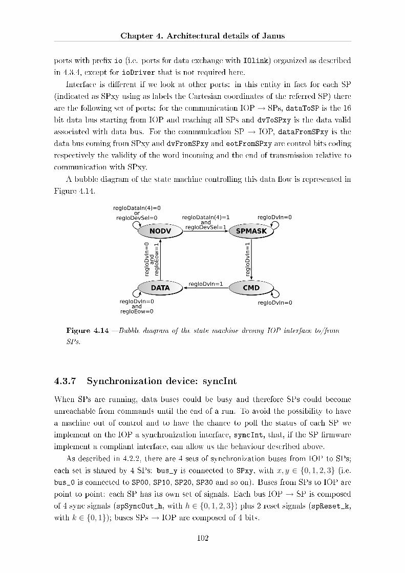
Chapter 4. Architectural details of Janus
ports with pre�x io (i.e. ports for data exchange with IOlink) organized as described
in 4.3.4, except for ioDriver that is not required here.
Interface is di�erent if we look at other ports: in this entity in fact for each SP
(indicated as SPxy using as labels the Cartesian coordinates of the referred SP) there
are the following set of ports: for the communication IOP → SPs, dataToSP is the 16
bit data bus starting from IOP and reaching all SPs and dvToSPxy is the data valid
associated with data bus. For the communication SP → IOP, dataFromSPxy is the
data bus coming from SPxy and dvFromSPxy and eotFromSPxy are control bits coding
respectively the validity of the word incoming and the end of transmission relative to
communication with SPxy.
A bubble diagram of the state machine controlling this data �ow is represented in
Figure 4.14.
Figure 4.14 � Bubble diagram of the state machine driving IOP interface to/from
SPs.
4.3.7 Synchronization device: syncInt
When SPs are running, data buses could be busy and therefore SPs could become
unreachable from commands until the end of a run. To avoid the possibility to have
a machine out of control and to have the chance to poll the status of each SP we
implement on the IOP a synchronization interface, syncInt, that, if the SP �rmware
implement a compliant interface, can allow us the behaviour described above.
As described in 4.2.2, there are 4 sets of synchronization buses from IOP to SPs;
each set is shared by 4 SPs: bus_y is connected to SPxy, with x, y ∈ {0, 1, 2, 3} (i.e.bus_0 is connected to SP00, SP10, SP20, SP30 and so on). Buses from SPs to IOP are
point to point: each SP has its own set of signals. Each bus IOP → SP is composed
of 4 sync signals (spSyncOut_h, with h ∈ {0, 1, 2, 3}) plus 2 reset signals (spReset_k,with k ∈ {0, 1}); buses SPs → IOP are composed of 4 bits.
102
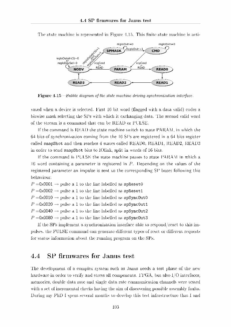
4.4 SP �rmwares for Janus test
The state machine is represented in Figure 4.15. This �nite state machine is acti-
Figure 4.15 � Bubble diagram of the state machine driving synchronization interface.
vated when a device is selected. First 16 bit word (�agged with a data valid) codes a
bitwise mask selecting the SPs with which it exchanging data. The second valid word
of the stream is a command that can be READ or PULSE.
If the command is READ the state machine switch to state PARAM, in which the
64 bits of synchronization coming from the 16 SPs are registered in a 64 bits register
called snapShot and then reaches 4 states called READ0, READ1, READ2, READ3
in order to send snapShot bits to IOlink, split in words of 16 bits.
If the command is PULSE the state machine passes to state PARAM in which a
16 word containing a parameter is registered in P . Depending on the values of the
registered parameter an impulse is sent to the corresponding SP buses following this
behaviour:
P =0x0001 → pulse a 1 to the line labelled as spReset0
P =0x0002 → pulse a 1 to the line labelled as spReset1
P =0x0010 → pulse a 1 to the line labelled as spSyncOut0
P =0x0020 → pulse a 1 to the line labelled as spSync0ut1
P =0x0040 → pulse a 1 to the line labelled as spSyncOut2
P =0x0080 → pulse a 1 to the line labelled as spSyncOut3
If the SPs implement a synchronization interface able to respond/react to this im-
pulses, the PULSE command can generate di�erent types of reset or di�erent requests
for status information about the running program on the SPs.
4.4 SP �rmwares for Janus test
The development of a complex system such as Janus needs a test phase of the new
hardware in order to verify and stress all components. FPGA, but also I/O interfaces,
memories, double data rate and single data rate communication channels were tested
with a set of incremental checks having the aim of discovering possible assembly faults.
During my PhD I spent several months to develop this test infrastructure that I and
103
Chapter 4. Architectural details of Janus
some other people of the Janus collaboration use during December 2007 to check all
the 19 boards built by Eurotech for the Janus collaboration. The e�ectiveness of this
test suite can be assessed by the fact that in less than one month all Janus boards
were successfully put into operation.
The incremental tests developed, from the simpler to the more complex, are:
01_uart_regs
Performs a reset via the serial interface; reads two con�guration registers; writes a
con�guration register; re-reads the written register.
Coverage: checks components driving serial link.
02_uart_int_mem
Performs a set of write and read operations on an FPGA internal memory via serial
link using sequential patterns and random patterns.
Coverage: check serial link and some FPGA structures.
03_uart_ext_mem
Performs a large set of write and read operations on the external staging memory
via serial link using sequential patterns and random patterns.
Coverage: checks the stability of the serial link and the integrity of the external
memory.
04_gbit_regs
Reads 29 registers of the PHY driving Gigabit link and check their values.
Coverage: checks the PHY integrity.
05_gbit_int_mem
Perform a set of write and read operations on an FPGA internal memory via
Gigabit link using sequential patterns and random patterns.
Coverage: check Gigabit link and some FPGA structures.
06_gbit_ext_mem
Performs a large set of write and read operations on the external staging memory
via Gigabit link using sequential patterns and random patterns.
Coverage: checks the stability of the Gigabit link and the integrity of the external
memory.
07_sync
First performs con�guration of all SPs via IOP con�guration interface with a basic
�rmware, then IOP pulses a value on synchronization lines of each SP; each SP
responds with the old value of the sync register x-ored with the value pulsed from
IOP. When IOP sends a synchronization reset (bit 0) all synchronization lines
from SP to IOP are pulled low; when IOP sends a synchronization reset (bit 1) all
104

4.4 SP �rmwares for Janus test
synchronization lines from SP to IOP are pulled high.
Coverage: checks SPs con�guration and synchronization interfaces.
08_iop_sp_comm
Resets the con�guration �rmware of all SPs, re-con�gures them and then checks
single ended lines IOP ↔ SP writing data coming from host PC in an internal
memory of the SPs. Re-reads data and checks their integrity.
Coverage: checks SPs con�guration and all data and controls lines IOP ↔ SP.
09_loop_2_sdr
Resets the con�guration �rmware of all SPs and re-con�gures them. Initializes with
di�erent values two memories of a pair of neighbours SP_A and SP_B. Following
a start command, two initialized SPs exchange between each other their memory
contents. The host PC polls the status via synchronization signals. When data
transfer SP_A ↔ SP_B ends, host PC dumps the memory contents and cross
checks that data of SP_A are stored onto memory within SP_B and vice versa.
Coverage: checks SPs con�guration and all di�erential pairs SP ↔ SP in all direc-
tions.
10_loop_2_ddr
The same of 09_loop_2_sdr but di�erential pairs SP ↔ SP works in double data
rate mode.
Coverage: check stability of double data rate on di�erential links.
11_loop_full_board
Performs a test of data transfer among all possible ring of SPs on a Janus board.
Coverage: checks stability in case of simultaneous load of all communication lines
on a board.
12_random_wheel
First intensive test in terms of FPGA resources: we implement 37 shift registers
each generating 32 random numbers per clock cycle. We store them in some bu�ers
and we check them after a �xed number of clock cycles. This �rmware requires
∼ 86% of the FPGA logic and ∼ 38% of the embedded RAM. Moreover this test
implement a system to check temperature of the FPGA.
Coverage: checks a complex situation of medium-high load.
13_sg640
Runs the �rst real spin glass simulation performing 640 spin update per clock cycle
on a lattice of 803 spins.
Coverage: checks a typical work load.
105
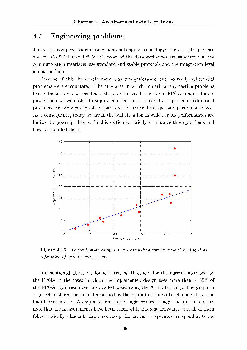
Chapter 4. Architectural details of Janus
4.5 Engineering problems
Janus is a complex system using non challenging technology: the clock frequencies
are low (62.5 MHz or 125 MHz), most of the data exchanges are synchronous, the
communication interfaces use standard and stable protocols and the integration level
is not too high.
Because of this, its development was straightforward and no really substantial
problems were encountered. The only area in which non trivial engineering problems
had to be faced was associated with power issues. In short, our FPGAs required more
power than we were able to supply, and this fact triggered a sequence of additional
problems that were partly solved, partly swept under the carpet and partly non solved.
As a consequence, today we are in the odd situation in which Janus performances are
limited by power problems. In this section we brie�y summarize these problems and
how we handled them.
Figure 4.16 � Current absorbed by a Janus computing core (measured in Amps) as
a function of logic resource usage.
As mentioned above we found a critical threshold for the current absorbed by
the FPGA in the cases in which the implemented design uses more than ∼ 85% of
the FPGA logic resources (also called slices using the Xilinx lexicon). The graph in
Figure 4.16 shows the current absorbed by the computing cores of each node of a Janus
board (measured in Amps) as a function of logic resource usage. It is interesting to
note that the measurements have been taken with di�erent �rmwares, but all of them
follow basically a linear �tting curve except for the last two points corresponding to the
106
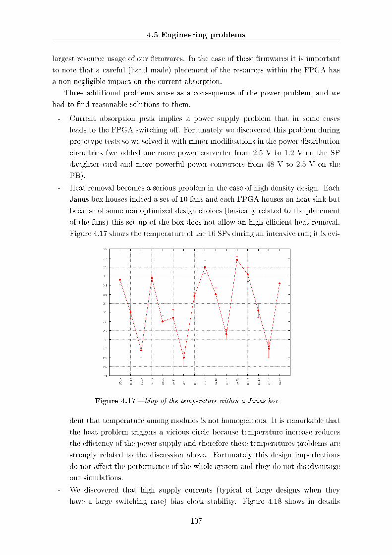
4.5 Engineering problems
largest resource usage of our �rmwares. In the case of these �rmwares it is important
to note that a careful (hand made) placement of the resources within the FPGA has
a non negligible impact on the current absorption.
Three additional problems arose as a consequence of the power problem, and we
had to �nd reasonable solutions to them.
- Current absorption peak implies a power supply problem that in some cases
leads to the FPGA switching o�. Fortunately we discovered this problem during
prototype tests so we solved it with minor modi�cations in the power distribution
circuitries (we added one more power converter from 2.5 V to 1.2 V on the SP
daughter card and more powerful power converters from 48 V to 2.5 V on the
PB).
- Heat removal becomes a serious problem in the case of high density design. Each
Janus box houses indeed a set of 10 fans and each FPGA houses an heat sink but
because of some non optimized design choices (basically related to the placement
of the fans) this set up of the box does not allow an high e�cient heat removal.
Figure 4.17 shows the temperature of the 16 SPs during an intensive run; it is evi-
Figure 4.17 � Map of the temperature within a Janus box.
dent that temperature among modules is not homogeneous. It is remarkable that
the heat problem triggers a vicious circle because temperature increase reduces
the e�ciency of the power supply and therefore these temperatures problems are
strongly related to the discussion above. Fortunately this design imperfections
do not a�ect the performance of the whole system and they do not disadvantage
our simulations.
- We discovered that high supply currents (typical of large designs when they
have a large switching rate) bias clock stability. Figure 4.18 shows in details
107
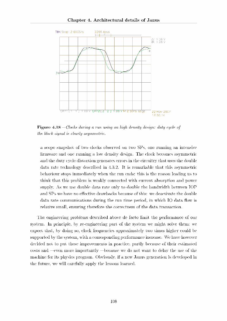
Chapter 4. Architectural details of Janus
Figure 4.18 � Clocks during a run using an high density design: duty cycle of
the black signal is clearly asymmetric.
a scope snapshot of two clocks observed on two SPs, one running an intensive
�rmware and one running a low density design. The clock becomes asymmetric
and the duty cycle distortion generates errors in the circuitry that uses the double
data rate technology described in 4.3.2. It is remarkable that this asymmetric
behaviour stops immediately when the run ends: this is the reason leading us to
think that this problem is weakly connected with current absorption and power
supply. As we use double data rate only to double the bandwidth between IOP
and SPs we have no e�ective drawbacks because of this: we deactivate the double
data rate communications during the run time period, in which IO data �ow is
relative small, ensuring therefore the correctness of the data transaction.
The engineering problems described above de facto limit the performance of our
system. In principle, by re-engineering part of the system we might solve them; we
expect that, by doing so, clock frequencies approximately two times higher could be
supported by the system, with a corresponding performance increase. We have however
decided not to put these improvements in practice, partly because of their estimated
costs and � even more importantly � because we do not want to delay the use of the
machine for its physics program. Obviously, if a new Janus generation is developed in
the future, we will carefully apply the lessons learned.
108

Bibliography
[1] Altera literature: Development Kits
http://www.altera.com/literature/ug/ug_stratix_pci_pro_kit.pdf 4.1
[2] Xilinx documentation: Virtex-4 Family Overview
http://www.xilinx.com/support/documentation/data_sheets/ds112.pdf
4.1
[3] Altera literature: Stratix II Devices
http://www.altera.com/literature/hb/stx2/stx2_sii5v1_01.pdf 4.1
[4] Xilinx documentation: Virtex-4 FPGA User Guide
http://www.xilinx.com/support/documentation/user_guides/ug070.pdf
4.1, 4.9, 4.10
[5] Xilinx web site:
http://www.xilinx.com/ise/optional_prod/cspro.htm 4.2.1
[6] Xilinx documentation: Virtex-4 FPGA Packaging and Pinout Speci�cation
http://www.xilinx.com/support/documentation/user_guides/ug075.pdf
4.2.1
[7] Xilinx documentation: Virtex-4 FPGA Con�guration User Guide
http://www.xilinx.com/support/documentation/user_guides/ug071.pdf
4.3.5
109

But I still haven't found what I'm looking for...
U2
5Performance and results
In this chapter I will present some relevant physics results obtained with the Janus
supercomputer. In �rst section I summarize some physics concepts useful for the
following discussions. In the second section I describe the features of the �rst run
performed in spring 2008: special care is provided to the performance and the cost of
the Janus system. Third section resumes concepts and results related with the �rst two
important runs of Janus: the simulation of the Edwards-Anderson spin glass model
and the simulation of the Potts model with four states.
Fundamental references for this chapter will be three of the most signi�cant articles
written thanks to the data produced by Janus: [1, 2, 3].
5.1 Useful concepts
5.1.1 About the equilibrium
In section 2.2.5 we look at the Monte Carlo methods as a way to �nd an equilibrium
con�guration for a model systems, but in some cases is interesting to discover the
behaviour of systems which are out of equilibrium using the same tools introduced in
previous chapter (see for instance 2.2.4). In studying these out-of-equilibrium systems
we are commonly interested in one of two things. Either we want to know how the
system relaxes from an initial state to equilibrium at a particular temperature, or we
are studying a system which never reaches equilibrium because it has a driving force
which continually pushes it into states which are far from equilibrium.
111
Chapter 5. Performance and results
The statistical mechanics of out-of-equilibrium systems is a less well-developed �eld
of study than that for equilibrium systems, and there is no one general framework to
guide our calculation such as we had in the equilibrium case. As the subject stands at
the moment at least, each system must be considered independently. In many cases
the mathematical hurdles to formulating an accurate analytic theory of a systems
behaviour are formidable.
For these reasons we decided to use the �rst run of the Janus system to investigate
out-of-equilibrium dynamics (see Sections 5.2 and 5.4 for more details).
5.1.2 Correlation
Even if a system is not ordered, there will in general be microscopic regions in the
material in which the characteristics of the material are correlated. Correlations are
generally measured through the determination of a two-point correlation function
Γ(r) = 〈ρ(0) · ρ(r)〉 (5.1.1)
where r is the spatial distance and ρ is the quantity whose correlation is being mea-
sured.
Below the phase transition, Γ(r) becomes large for all values of r, while it rapidly
decays to zero well above the critical temperature. The function Γ(r) takes into account
all the contributions to the correlation of ρ (for example, ρ can be the state of a spin),
even those due to external �elds. In order to measure only the part of correlation that
is due to internal �uctuations of the observable (e.g. only to the interactions between
spins) we de�ne the connected correlation function
ΓC(r) = 〈ρ(0) · ρ(r)〉 − |〈ρ〉|2 (5.1.2)
where we have discounted the overall alignment of the observable ρ. It is found that,
for T = TC but close to the critical temperature, and for r →∞, this term goes as
ΓC(r) ≈ r(d−1)/2e−r/ξ (5.1.3)
where d is the space dimensionality and ξ is a characteristic length of the system,
known as correlation length associated to the observable ρ.
When approaching the transition temperature TC from above, the interactions
within the system tend to become more and more relevant, and at the same time it
grows also the correlation between spatially well separated points of the system. The
correlation length ξ corresponds to the average distance at which di�erent parts of the
system present a correlation on the values of a given observable ρ: that is, 〈ρ(ri)ρ(rj)〉is signi�cant for |ri−rj| < ξ but tends to zero for larger distances. Typically ξ diverges
at TC . Equation 5.1.3 implies that the order parameter can normally �uctuate in blocks
of sizes up to ξ, while �uctuations of larger size are rather improbable [4, 5].
112
5.1 Useful concepts
It is also possible to consider correlations that are time-dependent. In this case the
system is prepared in a given initial con�guration and then the simulation is run for
a time tw (called waiting time). After the time tw the con�guration σ(tw) is stored.
From now on after each MC step the following correlation function is measured:
C(t, tw) =1
N
∑i
〈σi(t+ tw)σi(tw)〉 (5.1.4)
where 〈. . . 〉 means a thermal average (i.e. an average over di�erent realization of the
thermal noise, but the same initial con�guration) and the bar means an average over
di�erent realization of the bond-disorder [6].
5.1.3 Order parameters: magnetization and overlap
Phase transitions involve an abrupt change of some macroscopic properties of the
system, generally originating from a change in the microscopic structure of the system
under investigation. In the simplest cases this can be signaled by the observation of a
properly de�ned order parameter, i.e some property of the system which is identically
zero in the disordered phase and non-zero in the ordered phase. This change of behavior
when crossing the transition temperature, makes the order parameter a perfect marker
to spot the change of phase in the system when the transition occurs. An order
parameter is thus related to the global symmetries of the system. It is not possible to
give a generic de�nition of an order parameter, and it typically has to be de�ned in
a di�erent way for each physical system of interest. A considerable ingenuity is often
necessary to �nd a good order parameter to characterize a certain phase transition.
An example of order parameter in ferromagnetic materials (i.e. the Ising model)
is the magnetization M = 1/V∑
imi = 1/V∑
i〈si〉, where si is the value of the
magnetic moment at position i. The value of M changes from non-zero below the
phase transition, to zero above the critical temperature, and marks the change from
the ferromagnetic to the paramagnetic states.
We have seen that a characteristic of spin glasses is the lack of a uniform ordering,
substituted by a frozen disordered con�guration. This phase seems to possess a non-
zero local spontaneous magnetization mi = 〈si〉 , though the average magnetization
and any staggered magnetization vanish because of the absence of regularity in the
con�guration. Obviously neither of these observables can be used as an order param-
eter. It was noted by Edwards and Anderson that a correct description of the spin
glass phase should re�ect the lack of global orientation spin order in the frozen phase
(despite the local magnetization of the spins).
The �rst proper spin glass order parameter was proposed in the original EA work,
113
Chapter 5. Performance and results
and is thus known as the Edwards-Anderson parameter:
qEA =1
N
N∑i=1
〈si〉2 . (5.1.5)
This term vanishes in the paramagnetic phase, but it is non-zero if the local magneti-
zations mi are nonzero: this makes it a good order parameter for the transition from
paramagnetic to spin glass phase. The quantity qEA is actually a particular case of
a more general quantity called overlap, a statistical mechanics tool used to measure
the similarity of two di�erent con�gurations or replicas of a system. Given two spin
con�gurations a and b we de�ne their mutual overlap as:
qab =1
N
N∑i=1
sai · sbi , (5.1.6)
and it tells us how correlated a and b are. For example, for two replicas of an Ising
spins model we �nd the following possible values:
qab =
1 if a and b are completely correlated;
−1 if a and b are anti-correlated;
0 if a and b are completely uncorrelated;
(5.1.7)
5.2 First run details
We have followed the Monte Carlo dynamics of three cubic 803 spins lattices (all
initialized with random values, mimicking initial high-temperature conditions) at three
di�erent temperatures below Tc = 1.13 [7], i.e.
T1 = 0.8 = 0.70Tc ,
T2 = 0.7 = 0.62Tc ,
T3 = 0.6 = 0.53Tc .
(5.2.1)
We have performed 1011 Monte Carlo iterations for 96 independent samples at each
temperature (64 for T2). For comparison, the previous largest simulation of the same
model runs for 109 Monte Carlo iterations, for one temperature, 16 samples and a
smaller lattice of 603 sites [8]. The present simulation is altogether ' 2000 times more
compute intensive, allowing to come much closer to experimental time scales.
An interesting feature of the system is the size of the coherent domains. A clever
trick to measure this quantity is to simulate two copies of the system, {σ(1)i , σ
(2)i }
(evolving with the same set of couplings) for each samples. We de�ne the overlap
�eld at each lattice site as: qi = σ(1)i · σ
(2)i . The key observation is that, if lattice
points i and j belong to the same coherent domain, qi and qj tend to have the same
114
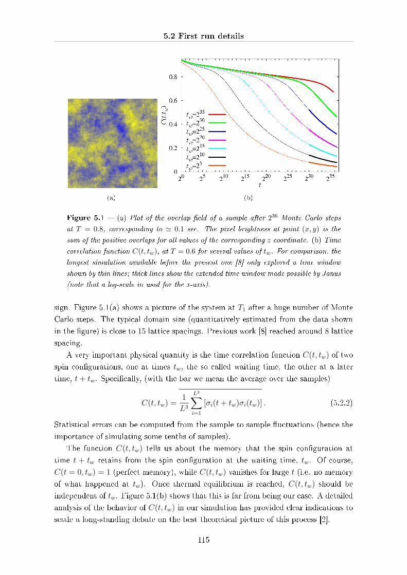
5.2 First run details
(a) (b)
Figure 5.1 � (a) Plot of the overlap �eld of a sample after 236 Monte Carlo steps
at T = 0.8, corresponding to ' 0.1 sec. The pixel brightness at point (x, y) is the
sum of the positive overlaps for all values of the corresponding z coordinate. (b) Time
correlation function C(t, tw), at T = 0.6 for several values of tw. For comparison, the
longest simulation available before the present one [8] only explored a time window
shown by thin lines; thick lines show the extended time window made possible by Janus
(note that a log-scale in used for the x-axis).
sign. Figure 5.1(a) shows a picture of the system at T1 after a huge number of Monte
Carlo steps. The typical domain size (quantitatively estimated from the data shown
in the �gure) is close to 15 lattice spacings. Previous work [8] reached around 8 lattice
spacing.
A very important physical quantity is the time correlation function C(t, tw) of two
spin con�gurations, one at times tw, the so called waiting time, the other at a later
time, t+ tw. Speci�cally, (with the bar we mean the average over the samples)
C(t, tw) =1
L3
L3∑i=1
[σi(t+ tw)σi(tw)] . (5.2.2)
Statistical errors can be computed from the sample to sample �uctuations (hence the
importance of simulating some tenths of samples).
The function C(t, tw) tells us about the memory that the spin con�guration at
time t + tw retains from the spin con�guration at the waiting time, tw. Of course,
C(t = 0, tw) = 1 (perfect memory), while C(t, tw) vanishes for large t (i.e. no memory
of what happened at tw). Once thermal equilibrium is reached, C(t, tw) should be
independent of tw. Figure 5.1(b) shows that this is far from being our case. A detailed
analysis of the behavior of C(t, tw) in our simulation has provided clear indications to
settle a long-standing debate on the best theoretical picture of this process [2].
115

Chapter 5. Performance and results
The simulation was performed in March 2008 on our 16 core Janus system. 6 + 6
cores have been used for T = 0.8 and 0.6 and 4 cores for T = 0.7 . The simulation
has executed almost continuously for approximately 25 days (20 days for simulation
at T = 0.7), apart from a 2 hours outage caused by snow-storm. A further Janus
core was used for checks, extensively verifying the reproducibility of selected segments
of the run. Simulation results (that is spin glass con�guration at appropriate Monte
Carlo times) were written onto disks attached to the Janus-host cluster. All in all
about 4 TBytes of disk space have been used.
All physically relevant averages (such as the overlap, C(t, tw), and many others)
have been computed on line on the Janus-host systems. Averages were computed as
soon as data became available: these tasks are not a computational bottleneck in our
case: just one or two host PCs are necessary to keep up with incoming data.
5.3 Janus performance
In this section, we assess the performance of our system in two di�erent ways:
- the number of e�ective operations per second.
- the speed-up factor (mostly in wall clock time, but also on other relevant metrics)
with respect to processor clusters or �arbitrary� size (i.e., assuming that, for the
given simulation, the optimal number of processor is actually deployed).
Let us �rst consider the number of e�ective operations performed by second. At
each clock cycle (clock frequency is 62.5 MHz), each SP processor updates 800 spins.
On a traditional architecture, this could require at least the following instructions for
each spin:
- 6 loads
- 1 sum (32 bits)
- 2 xor (32 bits)
- 6 sum (3 bits)
- 6 xor (3 bits)
- 1 load LUT
- 1 comp (32 bits)
- 6 updates of address pointers ( 1 mult, 1 sum )
- 1 store
- jump condition
We want to count only algorithm-relevant operation, so we do not count all load-
/store and address instructions; also, we count the 6 short xor and sum operations
116
5.3 Janus performance
as one each. We end up with 7 equivalent instruction for each spin update (shown in
italic in the list above). This translates into a processing power of 7× 800× 62.5× 106
operations per second, that is 350.0 Giga-ops. Our system operates 256 processors in
parallel, so it performs at the level of 89.6 Tera-ops.
From this (accurately measured) value and the cost �gures provided in [1] we obtain
our price performance ratio of 6.56 ¤ / Giga-ops. This �gure grows to 7.98 ¤ / Giga-
ops if we include the purchase costs of the items donated by our industrial partner.
Using the $ / ¤ exchange rate of 1.566 prevailing on April 4th, 2008, we obtain our
�nal �gure of 10.27 $ / Giga-ops (or 12.50 $ / Giga-ops if the costs of items donated
to the project are included).
Note that our system is also extremely energy e�cient at ' 8.75 Giga-ops / W
(for comparison, the top entry in the Green500 list is rated at 357.23 MFlops/W).
We now compare our performances to those obtained on commercial CPUs, where
spin-glass simulations have been performed so far. This analysis is mostly intended to
show the impact that our machine is going to have on the spin-glass community.
As stated in Section 2.3.2, the SMSC is the elective technique to handle Monte
Carlo simulation of large spin glass systems. The AMSC is only useful when dealing
with smaller lattice sizes, where equilibrium properties are investigated instead of slow
dynamics behavior, and a large set of sample statistics is needed.
The �gures given below refer to carefully programmed routines written in C, run-
ning on an IntelR© Core 2 DUO 64 bit CPU 2.4 GHz. In the multi-spin coding im-
plementation we also had some advantage in using C compilers supporting 128 bit
extended integer data types on 64 bit architectures (as the gcc 4.x releases do). A
further warning is associated to the fact that multi-spin coding e�ciency on tradi-
tional CPUs critically depend on whether the size of the simulated lattice is an integer
multiple or divisor of the CPU basic data word. While we cannot claim that our imple-
mentations are optimal, our judgment is that further optimization would not improve
performance by factors larger than 2 or 3, marginally a�ecting the qualitative picture
that we are outlining.
Our SMSC routine performs at 7.0 ns/spin average update rate when simulating
an L = 80 system. The AMSC routines available to us allows a 0.77 ns/spin update
rate, almost independently of the lattice size on modern CPUs equipped with large
cache memories. By contrast, our FPGA implementation performs at 0.020 ns/spin
for the L = 80.
Table 5.1 reports the total CPU time, the wall clock time and an estimate of the
total energy needed to accomplish the task of performing the 1011 Monte Carlo steps
presented in the sections above, in various cases of di�erent sample statistics (256
samples is the case relevant for physics, as discussed above). The three columns refer
respectively to Janus, to PCs using AMSC, and to PCs using SMSC. We assumed,
117
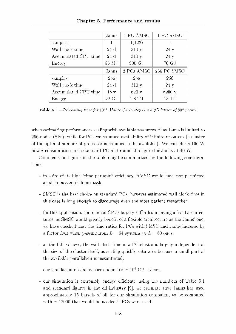
Chapter 5. Performance and results
Janus 1 PC AMSC 1 PC SMSC
samples 1 1(128) 1
Wall clock time 24 d 310 y 24 y
Accumulated CPU time 24 d 310 y 24 y
Energy 85 MJ 900 GJ 70 GJ
Janus 2 PCs AMSC 256 PC SMSC
samples 256 256 256
Wall clock time 24 d 310 y 24 y
Accumulated CPU time 18 y 620 y 6200 y
Energy 22 GJ 1.8 TJ 18 TJ
Table 5.1 � Processing time for 1011 Monte Carlo steps on a 3D lattice of 803 points.
when estimating performances scaling with available resources, that Janus is limited to
256 nodes (SPs), while for PCs we assumed availability of in�nite resources (a cluster
of the optimal number of processor is assumed to be available). We consider a 100 W
power consumption for a standard PC and round the �gure for Janus at 40 W.
Comments on �gures in the table may be summarized by the following considera-
tions:
- in spite of its high �time per spin� e�ciency, AMSC would have not permitted
at all to accomplish our task;
- SMSC is the best choice on standard PCs; however estimated wall clock time in
this case is long enough to discourage even the most patient researcher.
- for this application, commercial CPUs largely su�er from having a �xed architec-
tures, as SMSC would greatly bene�t of a �exible architecture as the Janus' one:
we have checked that the time ratios for PCs with SMSC and Janus increase by
a factor four when passing from L = 64 systems to L = 80 ones.
- as the table shows, the wall clock time in a PC cluster is largely independent of
the size of the cluster itself, as scaling quickly saturates because a small part of
the available parallelism is instantiated;
- our simulation on Janus corresponds to ' 104 CPU-years.
- our simulation is extremely energy e�cient: using the numbers of Table 5.1
and standard �gures in the oil industry [9], we estimate that Janus has used
approximately 15 barrels of oil for our simulation campaign, to be compared
with ' 12000 that would be needed if PCs were used.
118

5.4 Physics results overview
5.4 Physics results overview
After its commissioning, acceptance and reliability tests in April 2008, the large Janus
installation in Zaragoza was immediately used for two large scale simulations.
In the �rst simulation (whose results were also used for our submission to the 2008
Gordon Bell Prize), we studied the long term (in Monte Carlo time) evolution of a
large (803) Edwards-Anderson spin glass at several temperatures clearly below the
critical one. In this type of simulation, the physical focus is not on measuring physical
observables at the statistical equilibrium (reaching equilibrium for such a large system
is still out of question even for Janus); rather, we want to pinpoint several speci�c
features of how the system drifts within its con�guration space as it tries to move
toward more energetically favourable con�gurations. This is a relevant subject of
study, since several conjectures have been made, so it is important to compare with
experimental data.
In the second large simulation, we studied the 4-state Potts model (in 3D). In this
case, a much smaller lattice (163) was used and a serious attempt has been done to
bring the system into statistical equilibrium. In this case the ultimate goal of the
simulation was to characterize the structure and to measure the main parameters of
the phase transition of the system.
I describe in more details both simulations and their main physical results in the
following.
5.4.1 Non-equilibrium dynamics of a large EA spin glass
The results discussed in this section have been published in [1], where special attention
is given to the computational aspects of the simulation and in [2, 10] where the results
of the physical analysis are considered in details.
Below their glass temperature, experimental spin glasses are perennially out of
equilibrium. The understanding of their sophisticated dynamical behavior is a long
standing challenge both to theoretical and to experimental physics. On the simulation
side, it is only possible to bring to statistical equilibrium very small systems, so if
we study these small systems, we may expect that our �ndings are strongly a�ected
by �nite-size e�ects. On the other hand, several theoretical models try to highlight
correlations between the structure of the equilibrium con�gurations of a large spin glass
and the dynamics according to which that system slowly drifts toward equilibrium. If
we study numerically a large spin glass system out of equilibrium we may therefore
hope to extrapolate information on its equilibrium properties. In this sense, the two
approaches are complementary ways to study these systems.
The standard (experimental and numerical) approach to the study of an out-of-
equilibrium spin glass is the so-called direct quench. In these experiments, the spin
119

Chapter 5. Performance and results
glass is cooled as fast as possible to the working temperature below the critical one,
T < Tc. It is let to equilibrate for a waiting time, tw, its properties to be probed
at a later time, t + tw. For instance one may cool the spin glass in the presence of
an external �eld, which is switched o� at time tw. The so called thermoremanent
magnetization decays with time, but the larger tw is, the slower the decay.
In fact, there is strong evidence that, if the cooling is fast enough, the thermore-
manent magnetization depends upon t and tw only through the combination t/tw, for
a very large time window.
The time evolution is believed to be caused by the growth of coherent spatial
domains. Great importance is ascribed to the size of these domains. Domain size is
characterized by the coherence length ξ(tw), which can be measured experimentally
and has to be correctly estimated from numerical simulation. Therefore, in a large
simulation, one has to measure observables that lead to the de�nition and evaluation of
ξ(tw). This is the main raw-data of the simulation, that can then be used to compare
with theoretical expectation. In the rest of this section I focus on this work.
We simulated the dynamics of the Edwards Anderson model, de�ned in (2.1.5).
The system was simulated on a lattice of linear size L = 80 and on a smaller lattice
with L = 40, at several temperatures below and above the critical temperatures (which
is not known with high precision but was estimated in previous works to be close to
Tc ' 1.1). Several samples of the systems were simulated and a huge number of
Monte Carlo steps (up to 1011) was performed. The parameters of our simulation are
summarized in table 5.2.
L T MC steps Ns
80 0.6 1011 96
80 0.7 1011 63
80 0.8 1011 96
80* 0.9 2.8× 10¹⁰ 32
80 1.1 4.2× 10⁹ 32
80* 1.15 2.8× 10¹⁰ 32
80* 0.7 1010 768
40 0.8 2.2× 10⁹ 2218
Table 5.2 � Parameters of our simulations. The overall wall-clock time needed was
less than six weeks. We highlight with * the simulations performed after completion
of [3]. Recall that we take the critical temperature from [11], Tc = 1.109(10). The fullanalysis of spin con�gurations was performed o�-line.
We wrote to disk the spin con�gurations at all times of the form [2i/4]+ [2j/4], with
integer i and j (the square brackets stand for the integer part). Hence, our t and tware of the form [2i/4]. These spin con�gurations are the starting point for any analysis.
120

5.4 Physics results overview
It is common practice, followed in this work, to de�ne real replicas. These are two
statistically independent systems, {σ(1)x } and {σ(2)
x }, evolving in time with the very
same set of couplings. Their overlap �eld at time tw is:
qx(tw) = σ(1)x (tw)σ(2)
x (tw) (5.4.1)
The overlap is the basic quantity from which most observables are derived. For
instance, the spin glass order parameter is
q(tw) =1
N
∑x
qx(tw) (5.4.2)
The mean value of q(tw) over many samples vanishes in the non-equilibrium regime,
when the system size is much larger than the coherence length ξ(tw). So the spin glass
susceptibility,
χSG(tw) = Nq2(tw) (5.4.3)
that steadily grows with the size of the coherent domains, is a �rst approximate way
to measure the correlation length. More accurate estimation of the correlation length
are based on so called single time correlation functions
C4(r, tw) =1
N
∑x
qx(tw)qx+r(tw) (5.4.4)
The long distance decay of C4(r, tw) can be written according to the following
functional form:
C4((r, tw) =1
raf(r/ξ(tw)) (5.4.5)
In other terms, if we are able to estimate correctly ξ we are in a position to
reliably understand (from numerical or experimental data) the functional behaviour
of f , thereby clarifying the approach to equilibrium of the system.
In order to measure ξ in a model-independent way, we compute the integrals
Ik(tw) =
∫ ∞0
drrkC4(r, tw) (5.4.6)
If we take (5.4.5) into account, we see that
ξk,k+1 =Ik+1(tw)
Ik(tw)∝ ξ(tw) (5.4.7)
In principle this equation is valid for any k. In practice, for small k there is a
systematic error because (5.4.5) is only valid for large values of r. However, if we
increase k (thereby suppressing the contribution of small r to the integral) we meet
larger statistical error. In practice, the best trade-o� is for k = 1 (or, equivalently,
ξ1,2.). This is shown in Figure 5.2a. Using this technique, we are able to measure
121
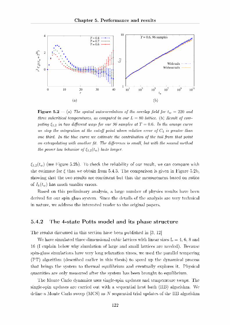
Chapter 5. Performance and results
(a) (b)
Figure 5.2 � (a) The spatial autocorrelation of the overlap �eld for tw = 220 and
three subcritical temperatures, as computed in our L = 80 lattice. (b) Result of com-
puting ξ1,2 in two di�erent ways for our 96 samples at T = 0.6. In the orange curve
we stop the integration at the cuto� point where relative error of C4 is greater than
one third. In the blue curve we estimate the contribution of the tail from that point
on extrapolating with another �t. The di�erence is small, but with the second method
the power law behavior of ξ1,2(tw) lasts longer.
ξ1,2(tw) (see Figure 5.2b). To check the reliability of our result, we can compare with
the estimate for ξ that we obtain from 5.4.3. The comparison is given in Figure 5.2b,
showing that the two results are consistent but that the measurement based on ratios
of Ik(tw) has much smaller errors.
Based on this preliminary analysis, a large number of physics results have been
derived for our spin glass system. Since the details of the analysis are very technical
in nature, we address the interested reader to the original papers.
5.4.2 The 4-state Potts model and its phase structure
The results discussed in this section have been published in [3, 12]
We have simulated three dimensional cubic lattices with linear sizes L = 4, 6, 8 and
16 (I explain below why simulation of large and small lattices are needed). Because
spin-glass simulations have very long relaxation times, we used the parallel tempering
(PT) algorithm (described earlier in this thesis) to speed up the dynamical process
that brings the system to thermal equilibrium and eventually explores it. Physical
quantities are only measured after the system has been brought to equilibrium.
The Monte Carlo dynamics uses single-spin updates and temperature swaps. The
single-spin updates are carried out with a sequential heat bath (HB) algorithm. We
de�ne a Monte Carlo sweep (MCS) as N sequential trial updates of the HB algorithm
122
5.4 Physics results overview
(i.e. every spin in the lattice undergoes a trial update once). The PT algorithm (ap-
plied to a given realization of the quenched disorder, that we will call a sample) is
based on simulating a number of copies of the system with di�erent values of the tem-
perature but the same interactions (the same set of Jij). Exchanging the temperature
of two copies with adjacent temperatures with a probability that respects the detailed
balance condition is the crucial mechanism of PT. The result is that each copy of the
system drifts in the whole allowed temperature range (that has been decided a priori).
When a copy is at a high temperature it equilibrates fast and so each time it descends
to low temperature it is likely to be in a di�erent valley in the energy landscape.
The simulation of the smaller lattices, with L = 4 and 6, was performed on standard
PCs, while Janus was used to simulate the larger lattices of linear size L = 8 and
L = 16. For this speci�c simulation, one Janus SP processor (one FPGA) is about
103 times faster that an Intel Core2DuoTMprocessor [13]. Janus has allowed us to
thermalize a large number of samples for bigger sizes than would have been feasible
on a standard computer. The computational e�ort behind our analysis amounts to
approximately 6 years CPU time on a 2.4 GHz Intel(R) Core2Duo(TM) processors for
L = 8 and thousands of CPU-years for L = 16.
Data input and output is a critical issue for Janus performance, so we had to
carefully choose how often to read con�guration data; in general, we end up taking
fewer measurements than in simulations on a traditional PC. Having fewer (but less
correlated) measurements does not a�ect the quality of our results. We read and
analyze values of physical observables every 2 × 10⁵ MCS. On the larger lattices, we
perform a PT step every 10 MCS while on the smaller lattices this value is 5. In a
standard computer the PT algorithm takes a negligible amount of time, compared to
a whole MCS. However, in Janus the clock cycles needed by one PT step are more
than those needed for a MCS. For this reason we chose to increase the number of MCS
between two PT steps. However, this number should not be too large, as we do not
want to negatively a�ect the PT e�ciency. A preliminary analysis has been carried
over to test how the PT parameter would a�ect the simulation results, and we have
selected a value that seems to be well optimized (see Table 5.3).
When performing such a large simulation, for which most of the expected results
live in a unknown space it is important to perform reasonable sanity checks on the
results of the simulation.
A standard test that a set of con�gurations are extracted from a thermalized sample
takes a given physical quantity and averages (�rst over the thermal noise and then over
the quenched disorder) over logarithmically increasing time windows. Equilibrium is
reached when successive values converge. We emphasize that it is crucial for time to
be plotted on logarithmic scale.
A typical quantity that is analyzed in this way is the correlation length of the
123
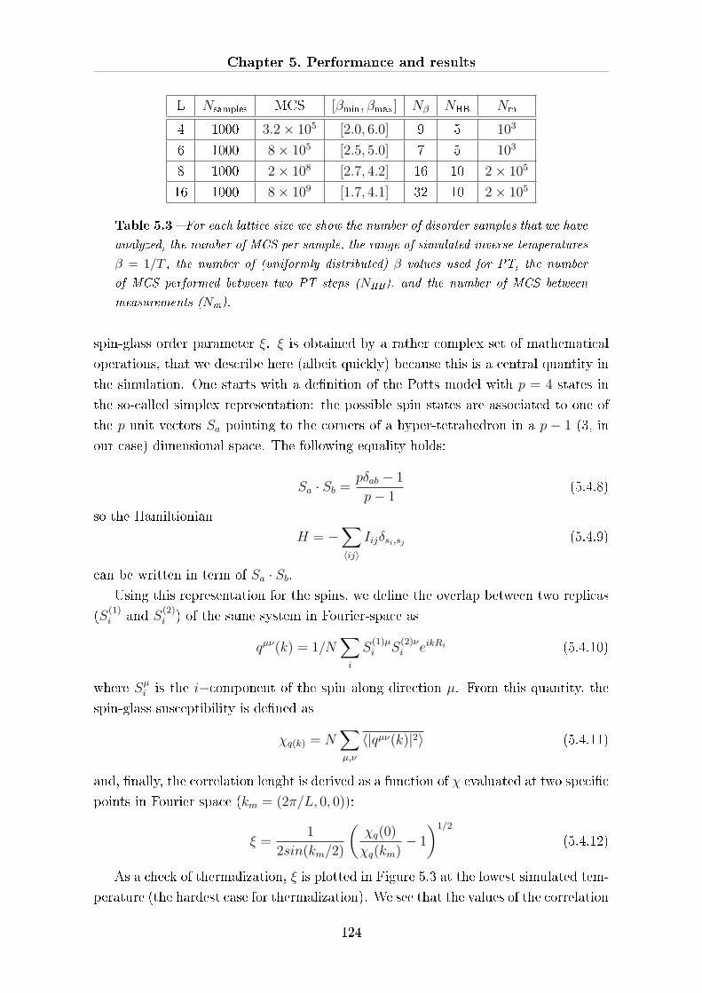
Chapter 5. Performance and results
L Nsamples MCS [βmin, βmax] Nβ NHB Nm
4 1000 3.2× 10⁵ [2.0, 6.0] 9 5 103
6 1000 8× 10⁵ [2.5, 5.0] 7 5 103
8 1000 2× 10⁸ [2.7, 4.2] 16 10 2× 10⁵
16 1000 8× 10⁹ [1.7, 4.1] 32 10 2× 10⁵
Table 5.3 � For each lattice size we show the number of disorder samples that we have
analyzed, the number of MCS per sample, the range of simulated inverse temperatures
β = 1/T , the number of (uniformly distributed) β values used for PT, the number
of MCS performed between two PT steps (NHB), and the number of MCS between
measurements (Nm).
spin-glass order parameter ξ. ξ is obtained by a rather complex set of mathematical
operations, that we describe here (albeit quickly) because this is a central quantity in
the simulation. One starts with a de�nition of the Potts model with p = 4 states in
the so-called simplex representation: the possible spin states are associated to one of
the p unit vectors Sa pointing to the corners of a hyper-tetrahedron in a p − 1 (3, in
our case) dimensional space. The following equality holds:
Sa · Sb =pδab − 1
p− 1(5.4.8)
so the Hamiltionian
H = −∑〈ij〉
Iijδsi,sj(5.4.9)
can be written in term of Sa · Sb.Using this representation for the spins, we de�ne the overlap between two replicas
(S(1)i and S(2)
i ) of the same system in Fourier-space as
qµν(k) = 1/N∑i
S(1)µi S
(2)νi eikRi (5.4.10)
where Sµi is the i−component of the spin along direction µ. From this quantity, the
spin-glass susceptibility is de�ned as
χq(k) = N∑µ,ν
〈|qµν(k)|2〉 (5.4.11)
and, �nally, the correlation lenght is derived as a function of χ evaluated at two speci�c
points in Fourier space (km = (2π/L, 0, 0)):
ξ =1
2sin(km/2)
(χq(0)
χq(km)− 1
)1/2
(5.4.12)
As a check of thermalization, ξ is plotted in Figure 5.3 at the lowest simulated tem-
perature (the hardest case for thermalization). We see that the values of the correlation
124
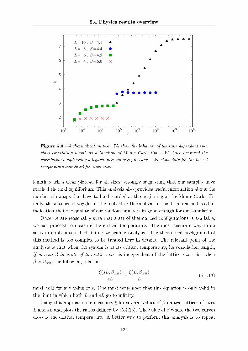
5.4 Physics results overview
Figure 5.3 � A thermalization test. We show the behavior of the time dependent spin
glass correlation length as a function of Monte Carlo time. We have averaged the
correlation length using a logarithmic binning procedure. We show data for the lowest
temperature simulated for each size.
length reach a clear plateau for all sizes, strongly suggesting that our samples have
reached thermal equilibrium. This analysis also provides useful information about the
number of sweeps that have to be discarded at the beginning of the Monte Carlo. Fi-
nally, the absence of wiggles in the plot, after thermalization has been reached is a fair
indication that the quality of our random numbers in good enough for our simulation.
Once we are reasonably sure that a set of thermalized con�gurations is available,
we can proceed to measure the critical temperature. The most accurate way to do
so is to apply a so-called �nite size scaling analysis. The theoretical background of
this method is too complex to be treated here in details. The relevant point of the
analysis is that when the system is at its critical temperature, its correlation length,
if measured in units of the lattice size is independent of the lattice size. So, when
β ' βcrit, the following relation
ξ(sL, βcrit)
sL=ξ(L, βcrit)
L(5.4.13)
must hold for any value of s. One must remember that this equation is only valid in
the limit in which both L and sL go to in�nity.
Using this approach one measures ξ for several values of β on two lattices of sizes
L and sL and plots the ratios de�ned by (5.4.13). The value of β where the two curves
cross is the critical temperature. A better way to perform this analysis is to repeat
125
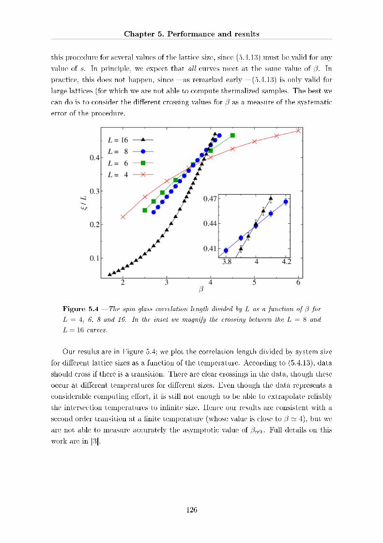
Chapter 5. Performance and results
this procedure for several values of the lattice size, since (5.4.13) must be valid for any
value of s. In principle, we expect that all curves meet at the same value of β. In
practice, this does not happen, since � as remarked early � (5.4.13) is only valid for
large lattices (for which we are not able to compute thermalized samples. The best we
can do is to consider the di�erent crossing values for β as a measure of the systematic
error of the procedure.
Figure 5.4 � The spin glass correlation length divided by L as a function of β for
L = 4, 6, 8 and 16. In the inset we magnify the crossing between the L = 8 and
L = 16 curves.
Our results are in Figure 5.4; we plot the correlation length divided by system size
for di�erent lattice sizes as a function of the temperature. According to (5.4.13), data
should cross if there is a transition. There are clear crossings in the data, though these
occur at di�erent temperatures for di�erent sizes. Even though the data represents a
considerable computing e�ort, it is still not enough to be able to extrapolate reliably
the intersection temperatures to in�nite size. Hence our results are consistent with a
second order transition at a �nite temperature (whose value is close to β ' 4), but we
are not able to measure accurately the asymptotic value of βcrit. Full details on this
work are in [3].
126
Bibliography
[1] F. Belletti et al., Janus: a Cost E�cient FPGA-Based Monte Carlo Simulation
Engine, technical report
http://df.unife.it/janus/papers/gbpaper_sub2.pdf. 5, 5.3, 5.4.1
[2] F. Belletti et al., Nonequilibrium spin-glass dynamics from picoseconds to a tenth
of a second, Phys. Rev. Lett. 101, 157201 (2008). 5, 5.2, 5.4.1
[3] A. Cruz et al., The Spin Glass Phase in the Four-State, Three-Dimensional Potts
Model, submitted to Phys. Rev. B (2009). 5, 5.2, 5.4.2, 5.4.2
[4] D. P. Landau, K. Binder A Guide to Monte Carlo Simulations in Statistical
Physics, Cambridge University Press (2005). 5.1.2
[5] D. Sciretti, Spin Glasses, Protein Design and Dedicated Computers, PhD thesis,
Instituto de Biocomputación y Física de Sistemas Complejos, September 2008.
5.1.2
[6] H. Rieger, Nonequilibrium dynamics and aging in the three-dimensional Ising
spin-glass model, J. Phys. A: Math. Gen. 26, 15, pp. 615-621 (1993). 5.1.2
[7] H. G. Ballesteros et al., Critical behavior of the three-dimensional Ising spin glass,
Phys. Rev. B 62, 14237 (2000). 5.2
[8] S. Jimenez et al., Ageing in spin-glasses in three, four and in�nite dimensions, J.
Phys. A: Math. and Gen, vol. 36, pp. 10755-10771 (2003). 5.2, 5.1
[9] A. Tripiccione, private communication. 5.3
[10] F. Belletti et al., An in-depth view of the microscopic dynamics of Ising spin
glasses at �xed temperature, submitted to J. Stat. Phys. (2008). 5.4.1
[11] M. Hasenbusch et al., The critical behavior of 3D Ising spin glass models: univer-
sality and scaling corrections, J. Stat. Mech. L02001 (2008); 5.2
[12] M. Guidetti, Simulating Potts Models on Janus, 10th Granada Seminar (2008).
5.4.2
127

BIBLIOGRAPHY
[13] F. Belletti et al., Simulating spin systems on Janus, an FPGA-based computer,
Comp. Phys. Comm., vol. 178, pp. 208-216 (2008). 5.4.2
128
Conclusions
Recon�gurable computing implies a completely di�erent approach to computing with
respect to the well known long-standing Von Neumann model. In place of a �xed
hardware structure that performs a given programmed algorithm, we con�gure un-
committed hardware resources so they behave in such a way that they process a data
stream according to the requirements of a given algorithm.
There are obvious large potential advantages in this approach; the main advan-
tage is the fact that a given budget of functional units (or logical operators) can be
fully con�gured to perform useful work for the considered algorithm. In recent years,
recon�gurable computing has become a viable approach, at the hardware level, as
Field Programmable Logic Arrays (FPGA) have established themselves as a techni-
cally sound, well understood and well supported technological paradigm for real-life
recon�gurable computing. Progress in FPGAs has been dramatic in the last decade
and their pace of development is expected to remain stable in the foreseeable future.
In spite of these encouraging situation, recon�gurable computing is still a niche
area in high-performance computing (and even more so in conventional computing,
with the only possible exception of embedded systems). This is so for reasons that
are probably as obvious as the potential advantages of this technology. In brief, a
recon�gurable devices de�nes a potentially enormous space of possible con�gurations,
in which only a very tiny subspace is the optimal (or maybe, even just satisfactory)
work-point for the implementation of a given algorithm. Locating this work-point is
a non-trivial endeavour for human intervention, that requires very speci�c skills and
long and tedious coding with appropriate Hardware Description Languages. Auto-
matic code-transformation tools, that start from a program written in a traditional
programming language and develop an appropriate con�guration for a recon�gurable
device are the only reasonable approach to make recon�gurable computing widespread
in the computing community, but at present their are hopelessly inadequate. A second
key problem in the area is the lack of well-de�ned, standardized interfaces between
the recon�gurable partition of a system and its host computer.
In this thesis, I have described my work in the framework of a large project (the
Janus project) that again shows the truly huge advantages o�ered by recon�gurable
129
Conclusions
computing for speci�c applications. The developments described here have increased
computing power available to a relevant and well-established application area in sta-
tistical physics by almost three orders of magnitude, rede�ning the state-of-the-art for
Monte Carlo simulations in condensed matter. Quite frankly, Janus has reached these
very important goals because the people that have developed the project (including
the writer of this document) have accepted to go through all the needed, complex
and tedious development steps. From this point of view, this work is frankly gives
very thin contributions to the broad area of making recon�gurable computing easier
to approach. However, Janus had to go around all these hurdles, so Janus experience,
including the de�nition of a reasonably �exible interface between Janus and its host,
may be an useful contribution.
The Janus system was developed by a collaboration of research centers and uni-
versities in Spain (Zaragoza, Madrid and Extremadura) and Italy (Ferrara and Rome)
with the industrial partnership of Eurotech. Its main goal was the development of
an e�cient system for Monte Carlo simulations of frustrated systems in condensed
matter, such as spin glasses. The speci�c computational features of the relevant simu-
lation algorithms is particularly well adapted to the architecture of currently available
recon�gurable devices.
During my PhD studies I have been deeply involved in the several activities asso-
ciated to the project:
- I have contributed to the overall architectural design of the system;
- I have de�ned the architectural structure of the interface between Janus and its
host computer;
- I have developed in all details the �rmware de�ning the Input Output processor
for the system;
- I have de�ned and developed in all details the set of test programs that have been
used to verify the correct behaviour of the Janus hardware;
- I have coordinated the installation and commissioning of the large Janus system
installed in Spain and of the smaller machine in Ferrara;
- I have worked on the development of a Janus-based application for the solution
of the coloring problem in large random graphs. This is an interesting attempt to
adapt recon�gurable hardware to a problem in which addressing is not as regular
as in spin-glasses. Encouraging results have been reached, even if it is clear that
present FPGAs have strong limitations to support these algorithms.
Physics simulations performed using Janus marks a new standard in the simulation
of complex discrete systems by allowing studies that would take centuries on traditional
computers. The system that we have developed has a very large sustained performance,
an outstanding price-performance ratio and an equally good power-performance ratio.
130
Conclusions
Janus is not a small scale laboratory prototype, but a large high-performance system,
able to run large simulations extending the state-of-the-art in the �eld and is an
example of high-performance recon�gurable computing.
131

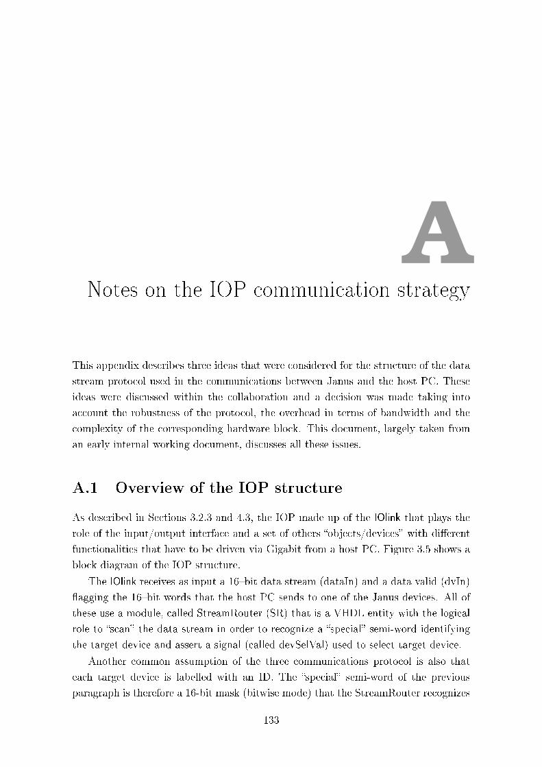
ANotes on the IOP communication strategy
This appendix describes three ideas that were considered for the structure of the data
stream protocol used in the communications between Janus and the host PC. These
ideas were discussed within the collaboration and a decision was made taking into
account the robustness of the protocol, the overhead in terms of bandwidth and the
complexity of the corresponding hardware block. This document, largely taken from
an early internal working document, discusses all these issues.
A.1 Overview of the IOP structure
As described in Sections 3.2.3 and 4.3, the IOP made up of the IOlink that plays the
role of the input/output interface and a set of others �objects/devices� with di�erent
functionalities that have to be driven via Gigabit from a host PC. Figure 3.5 shows a
block diagram of the IOP structure.
The IOlink receives as input a 16�bit data stream (dataIn) and a data valid (dvIn)
�agging the 16�bit words that the host PC sends to one of the Janus devices. All of
these use a module, called StreamRouter (SR) that is a VHDL entity with the logical
role to �scan� the data stream in order to recognize a �special� semi-word identifying
the target device and assert a signal (called devSelVal) used to select target device.
Another common assumption of the three communications protocol is also that
each target device is labelled with an ID. The �special� semi-word of the previous
paragraph is therefore a 16-bit mask (bitwise mode) that the StreamRouter recognizes
133

Appendix A. Notes on the IOP communication strategy
and �ags as a bitwise device selector.
StreamRouter analyzed obviously the other valid data words (containing informa-
tions for the devices) and forwards them with the suitable data valid (dvOut) to the
target devices (on the right of Figure 3.5).
A.2 First idea: the stu� byte
In this protocol it is assumed that a special semi-word (having for instance the value
0xAAAA) is inserted into the stream every time we want to send an information coding
the destination of the message. The StreamRouter can therefore easily identify the
�stu� semi-word� and consider the following 16-bit data word as the target devices
where addresses the following message. Is similar to an escape.
If at the time t the valid data coming from the IOlink is Dt = 0xAAAA then the
StreamRouter waits the next data Dt+1 (time t+ 1):
- if Dt+1 = Dt (green frame in the Figure A.1) then the data Dt+1 is not labelled
as a control data and goes to the target device with the value 0xAAAA. The value
of the dvOut is consequently set to high value and the devSelVal is deasserted (see
Figure A.2 for a timing diagram of this case);
- if Dt+1 6= Dt (violet frame in the Figure A.1) then the data coming from the
IOlink is labelled as control-data with the value Dt+1. The value of the devSelV
is set to high and the dvOut is pulled low (see Figure A.3 for a timing diagram);
in this case the data Dt+1 works as a device selection mask (devSelMask).
In both cases the �rst data Dt works as �stu� semi-word�, behaviour that gives the
name to this simple protocol. A typical stream of data is shown in �gure A.1.
Figure A.1 � Example of a stream with stu� byte.
A.2.1 Which stu�-value?
Using this data stream organization the address of a target device cannot have the
same value of the stu� word, or in other words, a mask coding a target device cannot
assume the same value of the stu�: in this case indeed the data Dt+1 is recognized
134
A.2 First idea: the stu� byte
Figure A.2 � Timing diagram in the case of the green frame of Figure A.1.
Figure A.3 � Timing diagram in the case of the violet frame of Figure A.1.
by the StreamRouter as a data of the previous message instead as a mask for a new
message.
This means that one of the 216 = 65536 possible values coded in the data Dt+1
should be used as stu� semi-word and cannot be used as mask to select target devices.
Ideally the mask that does not make sense is the null mask (0x0000) because the null
mask is the mask that selects no device. A natural value for the stu� seems to be
therefore the null mask (0x0000).
On the other hand the stu� should have a value that must be not to frequent in
the data stream in order to not degrade the bandwidth. For the spin-glass simulation
the value 0x0000 could be statistically many present in the data stream. Regular
structures as 0xAAAA or 0x5555 are sure a good stu� (are statistically few present in
the stream) but are �possible� masks.
A solution for this problem could be to implement a software data encoder/decoder
that analyzes the stream on the host PC and converts the stu� from 0x0000 to 0xAAAA
or 0x5555 and vice versa before the transmission.
A.2.2 Performance problem
To implement this data stream protocol the host PC sending data to a Janus device
have to check each outgoing data word to insert the stu� semi-word where/when
needed. This task should be performed run-time with an unde�ned and unpredictable
frequency. This may degrade the performance of the software driving Janus because
135

Appendix A. Notes on the IOP communication strategy
it could not possible to exploit contiguous memory bu�ers to pack data in advance.
A.3 Second idea: the tagged stream
The basic idea of this stream protocol is to introduce a tag before each message from
host PC to a Janus device. This tag distinguishes between command message and
data message. A 16-bit header gives therefore us two di�erent information:
- a tag codifying if the following data words are data or commands;
- a length that the StreamRouter uses as a counter of valid words before to start
to receive a new command.
The data stream is structured as shown in Figure A.4: in case of command message,
the 16-bit word following the header (green in Figure A.4) will be the mask codifying
the target devices.
Figure A.4 � Sample of a tagged stream.
A.3.1 Remarks
In this case the Janus software can perform an e�cient static memory bu�er allocation
because the protocol does not require changes of the message contents. The possible
performance problems introduced with the stu� byte protocol are here therefore solved.
A second comment is related to the logic structure of this stream organization: we
allows indeed the StreamRouter to distinguish between command messages and data
messages, that is not required and in some cases could introduce dependences between
Janus target devices and StreamRouter. Moreover, this protocol could appear as an
overkill for a system such as Janus, because the command messages in Janus are few
and very simple, so they do not require a special class of data exchange.
A.4 Third idea: the encapsulated stream
This third communication protocol proposed to handle the Janus data transaction
can be considered a generalization of the previous one. Each data set to send from
136
A.4 Third idea: the encapsulated stream
the host PC to a Janus device is called message with no di�erence between command
messages and data messages. Each message, moreover has an header (violet frame in
Figure 3.6) that gives to the StreamRouter information about the destination (mask
containing the ID of the target device) and the length of the message. Details of the
protocol are described in 3.2.3 and 4.3.
A.4.1 Pros and cons
We focused our attention on this last protocol and we accept to use it for Janus
because:
- it is relatively simple to realize both the hardware side and the software side.
Sending header information (basically the mask of the target device and the
length of the message) does not require to scan the entire data segment of the
message. As described above this allow us to exploit the allocation of bu�ers into
the memory and to send them with no bandwidth disadvantages.
- a message length of 2 16-bit words means that we need a 32 bit counter into the
FPGA, but allow us a stream of ∼ 109 words of 16 bit (∼ 64 GB). It is remarkable
that a data transmission that load a cubic con�guration with lattice size L = 100
for each FPGA, with their couplings, requires 16× 4× 1003 + ε ∼ 8 MB.
Using this protocol remains in all cases the problem that the Janus system become out
of control until all the data of a requested operation are not delivered. A stop/reset
command of the system is indeed not allowed during a command using this protocol.
137

Ringraziamenti
I am glad to thank all the kind people of the Janus Collaboration, the great team
that has worked by my side during these years and that has taught me with unlimited
patience. The ability of the collaboration to convert chaos into scienti�c results remains
for me forever a formative and beautiful mystery. Thank you!
I gratefully acknowledge the great job done by my two referees, dr. M. Alderighi
and dr. R. Baxter who read an almost in�nite sequence of preliminary drafts and
provided illuminating comments and useful suggestions. Their help de�nitely improved
the quality of my thesis; thank you very much, Monica and Rob.
I am grateful to prof. K. Pingali and prof. F. Wray who kindly opened the doors of
their institutes and welcomed me for very interesting collaboration experiences during
my PhD studies.
During my work I was supported by INFN, IUSS, BiFi and HPC Europe.
Al termine di questi tre anni di avventure vorrei inoltre ringraziare dapprima Lele,
vero Maestro di scienza e pazienza che con la sua umanità e saggezza mi ha mostrato
giorno dopo giorno la via da seguire e con la sua amicizia e �ducia ha fatto di questo
dottorato un'esperienza indimenticabile. È un mondo grande Lele, grazie!
Un caro pensiero e un grande ringraziamento va poi a Fabio, collega corretto e
collaborativo, ma prima ancora compagno di tante avventure, di tante serate, di tante
discussioni e di tanti consigli sinceri.
A Marco, fedele vicino di scrivania, tutta la mia gratitudine per aver sempre soppor-
tato con il sorriso sulle labbra il mio caratteraccio e la mia iper-attività in dipartimento.
Un pensiero a Giorgio, amico e collaboratore del progetto Janus che ha sempre gen-
erosamente fatto il tifo per me e per la collaborazione. Ad Annalisa un gioioso grazie
per la quotidianità che s'è condivisa in questi anni: grazie per esserci sempre stata.
Non potendo citare tutti, ringrazio poi con sincerità tutte le persone che hanno
condiviso con me questo cammino di tre anni: i colleghi del dipartimento, i collabo-
ratori di Eurotech che hanno allietato le mie trasferte in terra friulana, gli amici di
vecchia e vecchissima data che vivono accanto a me o sparsi in giro per il mondo a
rincorrere i loro sogni.
139
Ringraziamenti
Un grazie sincero va poi a mamma Graziana e papà Elio per aver sempre riposto
�ducia nelle mie scelte sopportandole e supportandole: grazie. A mio fratello Fabio e a
Erika riservo un a�ettuoso grazie per avermi sempre fatto guardare in alto, con l'a�etto
e la sincerità che solo loro sanno riservarmi. Grazie anche a Giancarlo, Annamaria e
Carla, che mi hanno �adottato� in tanti momenti speciali.
Manuela, semplicemente grazie!
140