uw-mems process design handbook v1
TRANSCRIPT

UW-MEMS DESIGN
HANDBOOK
VERSION 5.0

2
© Copyright 2010 by the Center for Integrated RF Engineering (CIRFE) at the
University of Waterloo, Waterloo, Ontario, Canada; All rights reserved.
Permission to use and copy the information contained herein for internal,
noncommercial purposes is hereby granted. Any distribution of this manual or
associated layouts or any part thereof is strictly prohibited without prior written
consent of CIRFE.
GDSII is a trademark of Calma, Valid, Cadence.
L-Edit and Tanner Database (TDB) are trademarks of Tanner Research Inc.
CoventorWare is the trademark of Coventor Inc.

3
Chapter 1: GOLD-Based Surface Micromachining Process ....................................................................... 4
Introduction .......................................................................................................................................... 4
Process Overview ............................................................................................................................ 4
Layer #1: Titanium Tungsten Bias Lines ..................................................................................... 5
Layers #2 & #3: First Dielectric ................................................................................................... 5
Layer #4: First Gold ...................................................................................................................... 5
Layer #5: Second Dielectric ...................................................................................................... 6
Layer #6: Anchor ......................................................................................................................... 6
Layer #7: Dimple .......................................................................................................................... 6
Layer #8 & #9: Second Gold ..................................................................................................... 7
Final Release Step ........................................................................................................................ 7
Chapter 2: UW-MEMS Layout Design Guidelines .................................................................................... 8
Introduction .......................................................................................................................................... 8
Design Rules: General Outlines .................................................................................................... 9
Design Rules: Overlaps & Enclosures ......................................................................................... 11
Material Properties ........................................................................................................................ 17
Chapter 3: UW-MEMS Layout Example ................................................................................................. 18
Layout Generation ............................................................................................................................ 18
Chapter 4: Design Submission ................................................................................................................ 21
UW-MEMS Layout Format ................................................................................................................. 21
Custom UW-MEMS Process .......................................................................................................... 21
Contact Information .................................................................................................................... 22
References ..................................................................................................................................... 23

4
CHAPTER 1: GOLD-BASED
SURFACE MICROMACHINING
PROCESS
INTRODUCTION
The UW-MEMS process is a research-oriented, cost effective, proof of concept, multi-user
microfabrication process for industries, universities and government agencies offered at
the University of Waterloo, Waterloo, Ontario, Canada. The process is gold-based surface
micromachining derived and developed from work carried out by the Center for
Integrated RF Engineering (CIRFE) at the University of Waterloo over the past years. It has
been used successfully to build several MEMS devices [1]-[8].
The following is a general description and user guide for the UW-MEMS process which is
optimized for many RF applications, such as contact and capacitive MEMS switches,
electrostatic varactors, phase shifters, tunable filters and impedance matching networks
as well as RF passives including transmission line circuits, planar inductors, interdigital and
metal-insulator-metal (MIM) capacitors and resistive lines. Nevertheless, the process is
also applicable to many other MEMS devices, such as micro-mirror devices and surface
micromachined inertial sensors. Accordingly, designers from all micro-scale engineering
disciplines are encouraged to submit their designs.
The guidelines in this handbook target users with a minimum of processing experience.
The design rules of UW-MEMS are detailed in chapter 2. Moreover, a detailed example is
provided in chapter 3 to illustrate the typical layouts that designers need to submit for
UW-MEMS.
PROCESS OVERVIEW
The UW-MEMS microfabrication process employs only seven masks, and it starts with a
0.025” thick Alumina substrate polished on both sides with a relative permittivity of 9.9
and loss tangent of 0.0001 at 1MHz.
The seven masks used for the entire fabrication are electron-beam-write chromium masks
that are produced from nine layout layers, which are detailed in the chapter 2. Up to this

5
stage, it is worth noting that more than one layer can be used to produce ONLY one
mask. This fact is implied in the second and seventh main steps shown below.
LAYER #1: TITANIUM TUNGSTEN BIAS LINES
After the RCA cleaning of the wafer, 50 nm TiW layer is sputtered and patterned using
the layer “TiW”.
Figure1.1: After patterning using Layer “TiW”
LAYERS #2 AND #3: FIRST DIELECTRIC
A 0.7 m SiO2 is deposited at 250⁰C by plasma enhanced chemical vapor deposition
(PECVD) and patterned using reactive ion etching (RIE). RIE is then used to strip away the
etch-mask photoresist. The pattern is formed using a single mask based on the layout
layers “D1” and “D1HOLE” combined.
Figure1.2: After patterning using Layers “D1” & “D1HOLE”
LAYER #4: FIRST GOLD
An evaporated 40nm Cr/70nm Au bilayer is deposited as a seed layer. A negative
photoresist (PR) mold is patterned by photolithography using layer “G1” and 1µm Au is
electroplated inside that mold. The mold and the seed layer are removed afterwards. Cr
serves no more than an adhesion layer for Au.
Figure1.3: After patterning using Layer “G1”

6
LAYER #5: SECOND DIELECTRIC
A 30nm of TiW is sputtered followed by the deposition of 0.7µm SiO2 PECVD at 250˚C. The
SiO2 and TiW layers are then dry etched in RIE in order to pattern them using “D2” layer.
TiW layer serves here as an adhesion layer between SiO2 and Au.
Figure1.4: After patterning using Layer “D2”
LAYER #6: ANCHOR OPENINGS
Spin coated Polyimide is used as the sacrificial layer for the Au structural layer in UW-
MEMS. Initially, it is coated to a thickness of 2.5µm; then, it is patterned by “A” layer in RIE
in order to etch the polyimide and fully open the anchor holes.
Figure1.5: After patterning using Layer “A”
LAYER #7: DIMPLE OPENINGS
Similar to anchor patterning, the dimples openings are performed in polyimide using an
RIE etching step using the pattern of “D” layer. The depth of the etching is set to be 1m.
Figure1.6: After patterning using Layer “D”

7
LAYERS #8 AND #9: SECOND GOLD
The second Au layer consists of sputtered 70nm Au seed layer and an electroplated Au
layer. The total thickness of Au is set to be 2µm, and it is used as the structural layer for all
the MEMS devices. A negative PR mold is used to pattern this layer based on the layout
layers “G2” and “G2R” combined appropriately.
Figure1.7: After patterning using Layers “G2” and “G2R”
FINAL RELEASE STEP
Before releasing the devices, the wafers are diced into individual dies according to the
dicing lines in the layout. The sacrificial layer is then removed in O2 plasma dry etching in
RIE. At this stage, the microfabrication of UW-MEMS devices is complete and the samples
are packaged for shipping to the customers.
Figure1.8: After releasing the device by stripping away all polyimide

8
CHAPTER 2: UW-MEMS LAYOUT
DESIGN GUIDELINES
INTRODUCTION
These design guidelines and rules were determined during the process development
stage and several microfabrication runs carried out at CIRFE cleanroom facility. The rules
identify the physical and geometrical limitations of individual process steps. The herein
presented guidelines are extremely important and must be considered at the design
stage. If the guidelines are not followed closely by UW-MEMS users, the fabricated
devices will not meet the specifications and will probably fail or malfunction.
In general, there are two types of rules. The first type of rules specifies the minimum
feature sizes and minimum feature separation distances within a single layout layer, i.e.
intra-layer design rules. The minimum feature size refers to the minimum side length of a
trace that is feasible using UW-MEMS. In other words, if this rule is violated there is no
guarantee that the feature will be produced on the wafer. Similarly, the minimum
separation distance between adjacent features must comply with the design rules in
order to be feasible. Failure to follow the minimum spacing design rule results in a
merged feature.
The second type of design rules specifies the inter-level crossovers (overlaps) and
separation distances. This is mainly imposed by the inevitable relative misalignment of the
different layout layers throughout fabrication, and it will be shortly detailed. Both types of
design rules are considered mandatory and should be followed closely by the designer.

9
DESIGN RULES: GENERAL OUTLINES
The layout design rules for the UW-MEMS process are explained in the following tables
and illustrated in schematic format following the tables. First, Table 1 outlines the different
layer names, corresponding material thicknesses as well as layer numbers and
description.
Table 1: Layer Names, Material Thicknesses, Layers Order, Layer Description and Comments
Table 2 outlines the layers that are used during the microfabrication process. Please note
that for the case of “Light Filed”, you draw the features that you want to be remained on
the wafer. For example, for TiW layer patterning, you draw the features or traces such as
bias lines. For the “Dark Field”, you draw the parts you want to be removed from the
corresponding layer such as release holes or openings for anchors and dimples. Please
pay special attention to this concept. Failure to do so will result in a reverse polarity
devices.
In other words, for D1HOLE and G2R, you draw only the location of dielectric openings
and release holes in gold, respectively. These layers will be subtracted from the D1 and
G2 layers by CIRFE personnel prior to printing the second and seventh lithographic masks.
Layer
Name
Material
Thickness
Layer
Order
Layer
Description Comments
“TiW” 50nm 1
Resistive
Voltage
Biasing
Resistive Layer
“D1” &
“D1HOLE”
0.7µm 2 & 3 Dielectric 0.7µm SiO2 to cover the bias
lines
“G1”
1µm 4
Conductive
Layer
40nm evaporated Cr + 70nm
evaporated Au + 0.9µm
electroplated Au
“D2” 0.7µm 5 Dielectric 50nm TiW + 0.7µm SiO2
“A” & “D” 2.5µm 6 & 7 Sacrificial
Layer
2.5µm Anchor and 1µm
Dimple openings
“G2” &
“G2R”
2µm 8 & 9 Conductive
Layer
70nm sputtered Au + 1.9µm
electroplated Au

10
Table 2: Layer Names, Layer Polarity Type and Comments
Layer Names Polarity Comments
“TiW” Light Field Patterning TiW
“D1” Light Field Patterning D1 without openings
“D1HOLE” Dark Field Additional layer for openings on
the D1 layer
“G1” Light Field Patterning G1
“D2” Light Field Patterning D2
“A” Dark Field Opening anchors between G1
and G2
“D” Dark Field
Dimples of G2 for contacts of the
switches as well as preventing
the stiction of large plates
“G2” Light Field Patterning G2
“G2R” Dark Field Additional layer for release holes
of the G2 layer.

11
Table 3 presents the lithographic mask numbers with the respective GDSII indices of their
constituting layout layers. GDSII is the only format that UW-MEMS accept from all users.
Please use the GDSII numbers that are specified in the table for each layout layer to
avoid confusion. Layers D1HOLE and G2R are just employed to create the openings in
the D1 layer and the release holes in G2 layer, respectively. No lithographic masks are
printed specifically for these layers. Please note that the dimples are meant for small
features. Nominal surface area is 10µm by 10µm. However, they can be used for long
lines, but it is recommended that the width of the lines be 10µm.
Table 3: UW-MEMS Masks and GDSII Layer Indices
Lithographic Mask Layer Name(s) GDSII
Index
Mask #1 TiW 101
Mask #2 D1 – D1HOLE 102 - 110
Mask #3 G1 103
Mask #4 D2 104
Mask #5 A 105
Mask #6 D 106
Mask #7 G2 – G2R 107 - 109
DESIGN RULES: OVERLAPS & ENCLOSURES
Generally, the following guidelines should be considered:
For overlaps and enclosures of the layers, up to 10m of misalignment between the
layers is assumed. This is due to the limitations of our photolithography system. This is
an advisory design rule.
TiW lines are designated for the DC bias lines with no current flow. This layer is very
thin, and it is not intended for power transfer.
The following outlines the specific layout design rules to which close attention must be
paid. It is worth emphasizing that the minimum feature size and minimum spacing
between features are limits to which the designers should strictly adhere. Ideally, adding
a 10m additional safety margin to these numbers may increase the yield of fabrication.
Users can have round, orthogonal or any arbitrary shape in your layout. The release holes must be 10m x 10m squares with edge to edge distances not exceeding 20µm. Please
do not use this layer to define geometries. The features are embedded to provide access
to underneath the structural layer during the release purposes.
12
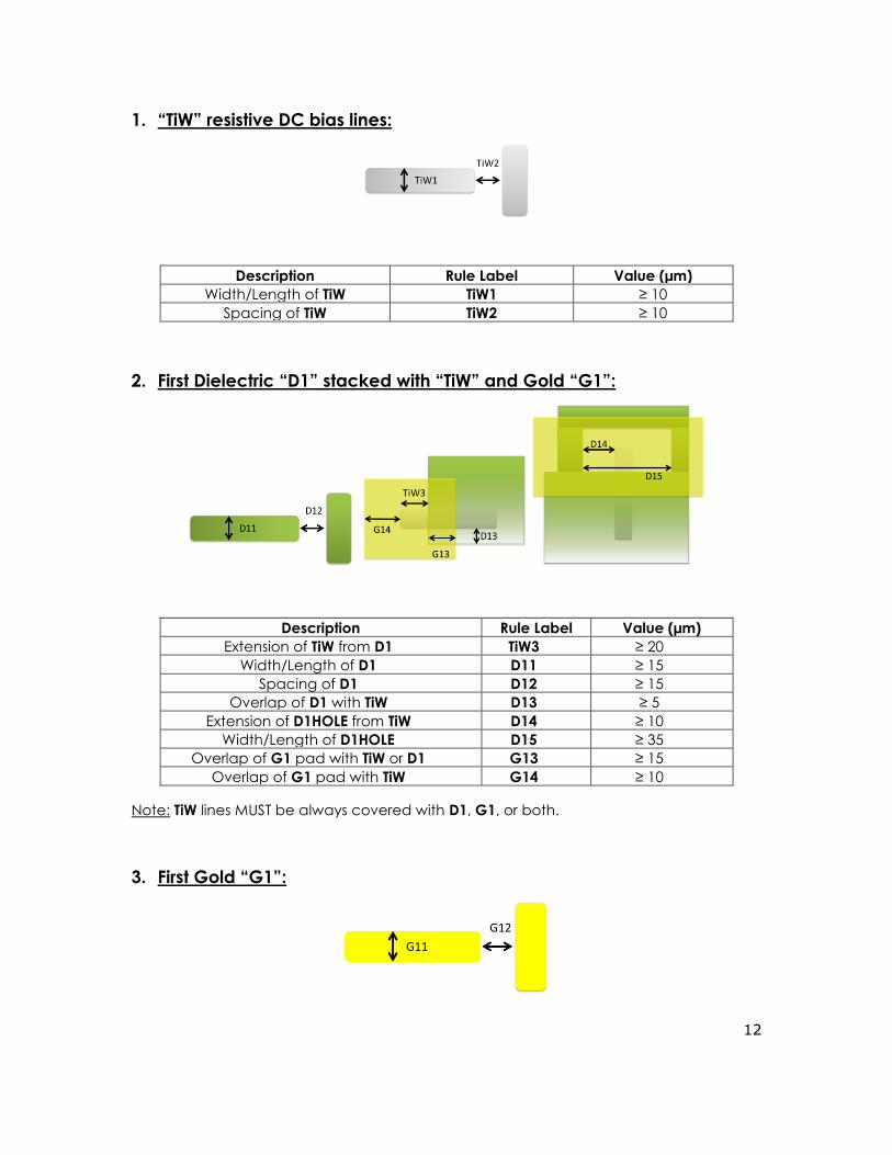
1. “TiW” resistive DC bias lines:
Description Rule Label Value (µm)
Width/Length of TiW TiW1 ≥ 10
Spacing of TiW TiW2 ≥ 10
2. First Dielectric “D1” stacked with “TiW” and Gold “G1”:
Description Rule Label Value (µm)
Extension of TiW from D1 TiW3 ≥ 20
Width/Length of D1 D11 ≥ 15
Spacing of D1 D12 ≥ 15
Overlap of D1 with TiW D13 ≥ 5
Extension of D1HOLE from TiW D14 ≥ 10
Width/Length of D1HOLE D15 ≥ 35
Overlap of G1 pad with TiW or D1 G13 ≥ 15
Overlap of G1 pad with TiW G14 ≥ 10
Note: TiW lines MUST be always covered with D1, G1, or both.
3. First Gold “G1”:

13
Description Rule Label Value (µm)
Width/Length of G1 G11 ≥ 10
Spacing of G1 G12 ≥ 10
4. Second Dielectric “D2” on top of TiW adhesion layer:
Description Rule Label Value (µm)
Width/Length of D2 D21 ≥ 15
Spacing of D2 D22 ≥ 15
Overlap of D2 with G1 D23 ≥ 10
Overlap of D2 with A D24 ≥ 15
Spacing of D2 from G1 D25 ≥ 15
Feature size of A over D2 AD ≤ 200
Note: D2 over 2 separated trances MUST be separated.
Note: Anchor on top of D2 cannot be used as mechanical support but can be used for
Metal-Insulator-Metal (MIM) capacitor.
5. Anchor “A” Openings:
Description Rule Label Value (µm)
Width/Length of A A1 ≥ 10

14
Spacing of A A2 ≥ 10
Overlap of G1 with A
(A MUST be covered with G1)
A3 ≥10
Overlap of G2 with A
(A MUST be covered with G2)
A4 ≥ 5
Spacing of D2 from A A5 ≥ 10

15
6. Dimple “D” Openings:
Description Rule Label Value (µm)
Width/Length of D DIM1 ≥ 10
Spacing of D DIM2 ≥ 10
Overlap of G2 with D DIM3 ≥ 5
Overlap of G1 with D DIM4 ≥ 5
7. Second Gold “G2”:
Description Rule Label Value (µm)
Width/Length of G2 G21 ≥ 10
Spacing of G2 G22 ≥ 10
Ratio of G23/G21 when G2 is not
anchored to G1
G23/G21 ≤ 30
Non-anchored length of G2 G23 ≤ 1200
Width/Length of G2R G24 ≥ 10
Spacing of G2R (edge-to-edge) G25 ≥ 20
Spacing of G2R from G2 edge G26 ≥ 10
Spacing of G2R from A G27 ≥ 10 & ≤ 30

16
8. Caution 1:
Note: This configuration results in short-circuit between the two G1 traces due to the
conductive TiW thin layer underneath the D2 layer.
9. Caution 2:
Note: This configuration may result in short-circuit between the G1 and G2 traces through
D2 layer.

17
MATERIAL PROPERTIES
Table 4 reports some of the mechanical and electrical properties of the UW-MEMS
process. The data is based on the measurements performed on earlier UW-MEMS
processes and agree well with the nominal known values in the literature. Designers can
use the existing values in the literature for the other material properties.
Table 4: Physical properties of UW-MEMS materials
*Higher resistivity (500Ω/) will be optionally available.
Material Residual Stress
(MPa)
Conductivity
( Ω-1/m)
Sheet Resistance
(Ω/)
Relative
Permittivity
TiW of
Resistive Bias
Lines
------ ------ 20* ------
SiO2 of D1 and
D2 ------ ------ ------ 4
Au of G1 and
G2
190 +/- 30%
Tensile 3.6х107 ------ ------

18
CHAPTER 3: UW-MEMS LAYOUT
EXAMPLE
LAYOUT GENERATION
This chapter presents a basic example of MEMS relay to illustrate the UW-MEMS layout
generation step-by-step for designers. Experienced designers typically use tools such as
L-EDIT and Cadence to generate the layouts for the various layers. However, any tool
that can generate layouts in GDSII formats can be used to submit designs to UW-MEMS.
This example is given to provide beginners in the field with layout illustrations to help them
understand the guidelines given in chapter 2.
Consider the MEMS relay shown in Figure 3.1. The relay consists of a cantilever beam
anchored to an input signal line. The cantilever can be pulled down using electrostatic
actuation so that its tip makes contact with the output signal line and hence closes the
relay. The actuation is performed using a pad covered by SiO2 (i.e. dielectric). The two
DC bias pads are connected to the actuation pad and the input signal line using high
resistivity TiW traces. A dimple is added to the cantilever tip to ensure contact with the
output signal line. Below is a description of the seven masks used for production of a
MEMS relay based on the nine layout layers detailed in chapters 1 and 2.
Fig. 3.2a shows the layout of Mask #1 (produced from “TiW” layer). This mask
shows the two high resistivity traces that connect the DC bias pads to the
actuation pad and the input signal line. The mask is “Light Field”. Note that the
TiW traces must be made at least 20 µm longer on each side in order to overlap
the gold (see Design Rules: Overlaps & Enclosures).
Fig. 3.2b shows the layout of Mask #2 (produced from “D1” and “D1HOLE” layers).
This mask shows the insulation layer that covers the bias lines. The mask is “Light
Field”.
Fig. 3.2c shows the layout of Mask #3 (produced from “G1” layer). This mask
shows the input/output signal lines, actuation electrode and the two bias pads.
The mask is “Light Field”.
Fig. 3.2d shows the layout of Mask #4 (produced from “D2” layer). This mask shows
the insulation layer that covers the actuation electrode. The mask is “Light Field”.
Fig. 3.2e shows the layout of Mask #5 (produced from “A” layer). This mask
defines the anchor location for connection of G2 and G1 metals. The mask is
“Dark Field”.
Fig. 3.2f shows the layout of Mask #6 (produced from “D” layer). This mask defines
the dimple location which is connected to the tip of the cantilever. The mask is
“Dark Field”.
Fig. 3.2g shows the layout of Layer #8 (“G2”). This layer shows the cantilever. The

19
layer is “Light Field”. Besides, Fig. 3.2h shows the layout of Layer #9 (“G2R”) that is
“Dark Field”. This layer will be subtracted from “G2” layer mask by CIRFE personnel
to generate the Mask #7.
Note:
The cantilever length needs to be extended at the anchor location in order to make sure
that “G1” and “G2” enclose “A” (see Design Rules: Overlaps & Enclosures).
Figure 3.1: A MEMS Relay
Figure 3.2a: Mask #1 (“TiW”) Figure 3.2b: Mask #2 (“D1” - “D1HOLE”)
Figure 3.2c: Mask #3 (“G1”) Figure 3.2d: Mask #4 (“D2”)

20
Figure 3.2e: Mask #5 (“A”) Figure 3.2f: Mask #6 (“D”)
Figure 3.2g: Layer ”G2” Figure 3.2h: Layer ”G2R”

21
CHAPTER 4: DESIGN SUBMISSION
UW-MEMS LAYOUT FORMAT
Designs should be submitted in GDSII format. Tanner L-Edit is the recommended layout
software. However, most of the other layout software tools can export to GDS format
including CoventorWare. A template for this process can be found on our website. The
layers should match the numbers posted in Table 3 of this handbook.
Please visit our website for more information:
www.cirfe.uwaterloo.ca
CUSTOM UW-MEMS PROCESS
CUSTOM UW-MEMS PROCESSES
The CIRFE facility has capability to provide a modified version of the UW-
MEMS process on a case by case basis. Designers will be able to select
thickness of materials, type of structural and sacrificial layers and number of
layers. The CIRFE facility also offers a variety of thin film metal and dielectric
deposition services.
For inquiry about the CUSTOM UW-MEMS Processes, please e-mail:

22
CONTACT INFORMATION
For questions or general inquiry about the UW-MEMS process, please send your e-mails
to:
Updates to this design handbook and further details about the CIRFE facility can be found
on our website at:
www.cirfe.uwaterloo.ca

23
REFERENCES
[1] M. Daneshmand and R. R. Mansour, (2007) “Redundancy RF MEMS Multiport Switches
and Switch Matrices”, Journal of Microelectromechanical Systems, Vol. 16, no. 2, pp.
296-303.
[2] M. Daneshmand and R. R. Mansour, (2006) “C-type and R-type RF MEMS Switches for
Redundancy Switch Matrix Applications”, IEEE MTT-S, pp.144-147.
[3] M. Daneshmand and R. R. Mansour, (2006) “Monolithic RF MEMS Switch Matrix
Integration”, IEEE MTT-S, pp. 140 –143.
[4] R. Al-Dahleh and R.R. Mansour, (2007) “A Novel Warped-Beam Design that Enhances
RF Performance of Capacitive MEMS Switches,” IEEE MTT-S, pp. 1813-1816.
[5] W. D. Yan and R. R. Mansour, (2007) “Compact Tunable Bandstop Filter Integrated
with Large Deflected Actuators,” IEEE MTT-S, pp.1611-1614.
[6] K. Chan, M. Daneshmand, R. R. Mansour, and R. Ramer, (2008) “Monolithic Crossbar
MEMS Switch Matrix,” IEEE MTT-S, pp. 129-132 (student paper award).
[7] F. Domingue, A. Kouki and R. R. Mansour, (2008) “Improved Distributed MEMS
Matching Network for Low Frequency Applications Using a Slow-Wave Structure,” IEEE
MTT-S, pp. 1279-1282.
[8] S. Fouladi, A. Akhavan Fomani, and R. R. Mansour, (2008) “A Novel Reconfigurable
Impedance Matching Network Using DGS and MEMS Switches for Millimeter-Wave
Applications”, IEEE MTT-S, pp. 145-148.