validation and standardization of thermal models -...
TRANSCRIPT

Confidential
ICT-2009.3.2-248603-IP
Modelling, Control and Management of Thermal Effects in Circuits of the Future
WP no. Deliverable no. Lead participant
WP7 D7.1.1 NXP-NL
Validation and standardization of thermal models
Prepared by M. Willemsen
Issued by THERMINATOR Project Office
Document Number THERMINATOR/D7.1.1/v1
Dissemination Level CONFIDENTIAL
Date 01/02/2013
© Copyright 2010-2013 STMicroelectronics, Intel Mobile Communication, NXP
Semiconductors, GRADIENT DESIGN AUTOMATION , MUNEDA, SYNOPSYS ,
BUDAPESTI MUSZAKI ES GAZDASAGTUDOMANYI EGYETEM , CSEM,
FRAUNHOFER , IMEC, CEA-LETI, OFFIS, Politecnico di Torino, ALMA MATER
STUDIORUM -Universita’ Di Bologna, ST-Polito.

THERMINATOR FP7 ICT – 2009.3.2 - 28603 D7.1.1
Confidential Page 2 01/02/2013
Document Title Validation and standardization of thermal models
Type Deliverable CO
Ref D7.1.1
Target version V1_1
Current issue V0_1
Status released
File
Author(s) W. Moering (NXP-D), A. Burenkov (FHG), J. Lorenz (FHG), M.
Willemsen (NXP-NL), S. Sque (NXP-NL), G. Greco (ST), H. Oprins
(IMEC), S. Stoffels (IMEC), R. Mahnkopf (IMC), C. Fiegna (UNIBO), T.
Cilento (SNPS-CH), S. Ress (BME)
Reviewer(s) V. Melikyan (SNPS-AM), D. Rossi (UNIBO)
Approver(s) G.Gangemi(ST)
Approval date 01/02/2013
Release date
Distribution of the release Dissemination level CO
Distribution list
History
Rev. DATE Comment
0.1 22-01-2013 Initial version
1.0 29-01-2013 Revised version, approved by all partners
1.1 01/02/2013 Check and ship out
THERMINATOR FP7 ICT – 2009.3.2 - 28603 D7.1.1
Confidential Page 3 01/02/2013
References [1] M. Ciappa, F. Carbognani, W. Fichtner: "Lifetime Prediction and Design of
Reliability Tests for High Power Devices in Automotive Applications ", IEEE
TRANSACTIONS ON DEVICE AND MATERIALS RELIABILITY, Vol 3, N0.
4,December 2003.
[2] Letor, S. Russo, R. Crisafulli “Life time prediction and design for reliability of
Smart Power devices for automotive exterior lightining “CIPS2008” proceedings”
[3] Therminator Deliverable D1.3.1 “Technical specification of testcases and
distribution to partners of concern”
[4] Therminator Deliverable D1.1.1 “Preliminary measurement data for various types
of devices”
[5] Therminator Deliverable D2.1.2 “Model based comparison of temperature effects
on device parameters for different technology nodes”
[6] Therminator Deliverable D7.2.1 “Demonstration of thermal-aware design
techniques
[7] A. Burenkov, J. Lorenz, Fraunhofer IISB, D2.1.4: Evaluation of self-heating
effects in devices and compact thermal models for advanced device structures,
THERMINATOR project office, 2012
[8] ITRS, International Technology Roadmap for Semiconductors. 2009 Update.
<www.itrs.net>, 2009.
[9] Sentaurus TCAD, Version G-2012.06, Synopsys Inc., Mountain View, CA, USA,
2012.
[10] C. Fiegna, Y. Yang, E. Sangiorgi, A. G. O’Neill, Analysis of self-heating
effects in ultrathin-body SOI MOSFETs by device simulation, IEEE Trans.
Electron. Dev. 55 (2008) pp. 233–244.
[11] T.-Y. Chiang, K. Banerjee, K. C. Saraswat, Analytical thermal model for
multilevel VLSI interconnects incorporating via effect, IEEE Electron Device
Lett. 23 (2002) pp. 31–33.
[12] M. Hinz, O. Marti, B. Gotsmann, M. A. Lantz, U. Dürig, High resolution
vacuum scanning thermal microscopy of HfO2 and SiO2, Appl. Phys. Lett. 92
(2008) pp. 43122–43123.
[13] Therminator deliverable D2.1.3 "Numerical comparison of self heating in
traditional (bulk, SOI) CMOS technologies & advanced (GaN) ones”
[14] Sentaurus Synopsis, ver.X-2005.10
[15] A. J. Scholten et al., IEEE IEDM 2009 Proceedings
[16] L. T. Su et al., IEEE TED, vol.41(1), pp.69, 1994
[17] J. D. Bude, Proc. Int. Conf. SISPAD, pp.23, 2000
[18] W. Liu et al., IEEE TED, vol.53(8), p.1868, 2006
[19] Beyne, E. “The Rise of the 3rd Dimension for System Integration”, Proc. IEEE
IITC, pp. 1-5, 2006.
[20] Garrou, Ph. (ed.), Handbook of 3D-Integration, Wiley-VCH, 2008.
[21] Leduc, P.; de Crecy, F.; Fayolle, M.; Charlet, B.; Enot, T.; Zussy, M.; Jones,
B.; Barbe, J.-C.; Kernevez, N.; Sillon, N.; Maitrejean, S.; Louisa, D.; , "Challenges
for 3D IC integration: bonding quality and thermal management," International
Interconnect Technology Conference, IEEE 2007 , vol., no., pp.210-212, 4-6 June
2007.
[22] Lau, J. H.; , "Evolution and outlook of TSV and 3D IC/Si integration,"
Electronics Packaging Technology Conference (EPTC), 2010 12th , vol., no.,
pp.560-570, 8-10 Dec. 2010.

THERMINATOR FP7 ICT – 2009.3.2 - 28603 D7.1.1
Confidential Page 4 01/02/2013
[23] Agonafer, D.; Kaisare, A.; Hossain, M.;. , Lee, Y.; Dewan-Sandur, B.; P. ,
Dishongh, T.; Pekin, S.; “Thermo-Mechanical Challenges in Stacked Packaging”,
Heat Transfer Engineering, Vol. 29(2), 134 – 148, 2008.
[24] Rencz, M.; Székely V.; “Structure function evaluation of stacked dies”,
Proceedings of the XXth SEMI-THERM Symposium, March 9-11, San Jose, CA,
USA, pp 50-55, 2004.
[25] Zhang, L.; Howard, N.; Gumaste, V.; Poddar, A.; Nguyen, L.; “Thermal
Characterization of Stacked-Die Packages”, 20th IEEE SEMI-THERM
Symposium, pp. 55-63, 2004.
[26] Van der Plas, G.; Limaye, P.; Loi, I.; Mercha, A.; Oprins, H.; Torregiani, C.;
Thijs, S.; Linten, D.; Stucchi, M.; Katti, G.; Velenis, D.; Cherman, V.;
Vandevelde, B.; Simons, V.; De Wolf, I.; Labie, R.; Perry, D.; Bronckers, S.;
Minas, N.; Cupac, M.; Ruythooren, W.; Van Olmen, J.; Phommahaxay, A.; de
Potter de ten Broeck, M.; Opdebeeck, A.; Rakowski, M.; De Wachter, B.; Dehan,
M.; Nelis, M.; Agarwal, R.; Pullini, A.; Angiolini, F.; Benini, L.; Dehaene, W.;
Travaly, Y.; Beyne, E.; Marchal, P.;, "Design Issues and Considerations for Low-
Cost 3-D TSV IC Technology," Solid-State Circuits, IEEE Journal of , vol.46,
no.1, pp.293-307, Jan. 2011.
[27] Swinnen, B.; Ruythooren, W.; De Moor, P.; Bogaerts, L.;Carbonell, L.; De
Munck, K. ; Eyckens, B.; Stoukatch, S. ; Sabuncuoglu Tezcan, D.; Tokei, Z.;
Vaes, J. ; Van Aelst, J. and Beyne, E.; “3D integration by Cu-Cu thermo-
compression bonding of extremely thinned bulk Si die containing 10μm pitch
through Si vias”, Proc. IEDM Conference, December 11-13, 2006, San Fransisco.
[28] Swinnen, B.; Jourdain, A. ; De Moor, P. ; Beyne E.; Chapter in Wafer Level 3-
D ICs Process Technology; edited by S. Tan, R.J. Gutmann, and L.R. Reif (Eds),
Springer, ISBN 978-0-387-76532-7, 2008.
[29] Jourdain, A.; Soussan, P.; Swinnen, B.; Beyne, E.; , "Electrically yielding
Collective Hybrid Bonding for 3D stacking of ICs," Electronic Components and
Technology Conference, 2009. ECTC 2009. 59th , vol., no., pp.11-13, 26-29 May
2009.
[30] http://www.mentor.com/products/mechanical/products/t3ster/
[31] Methodology for the Thermal Measurement of Component Packages (Single
Semiconductor Device) JEDEC Standard JESD51
[32] Transient dual interface test method for the measurement of the thermal
resistance junction-to-case of semiconductor devices with heat flow through a
single path. JEDEC Standard JESD51-14, Nov 2010
[33] P.Szabo, O.Steffens, M.Lenz, and G.Farkas, "Transient junction-to-case
thermal resistance measurement methodology of high accuracy and high
repeatability", Proc. 10th THERMINIC, Sofia-Antipolis, pp. 145-150, 2004

THERMINATOR FP7 ICT – 2009.3.2 - 28603 D7.1.1
Confidential Page 5 01/02/2013
This page was intentionally left blank.
THERMINATOR FP7 ICT – 2009.3.2 - 28603 D7.1.1
Confidential Page 6 01/02/2013
Contents
Document ................................................................................................................................... 2
Distribution of the release .......................................................................................................... 2
References .................................................................................................................................. 3
1 Introduction ........................................................................................................................... 9
2 Compact electro-thermal modelling (NXP-NL) ................................................................. 10
2.1 Introduction ................................................................................................................ 10
2.2 Technical results ........................................................................................................ 11
2.2.1 Validation of the thermal models for RF-LDMOS and GaN-HEMT with
measurements ..................................................................................................................... 11
2.2.2 Validation of the electro-thermal compact model with numerical calculations ... 19
2.2.3 Validation on different types of device ................................................................ 22
2.2.3.1 GaN Schottky diodes ........................................................................................ 24
2.2.3.2 SOI-LDMOS ..................................................................................................... 29
2.3 Conclusions ................................................................................................................ 32
3 Verification of TCAD (SNPS-CH, together with IMC, IMEC, ST, NXP-D) .................... 33
3.1 Introduction ................................................................................................................ 33
3.2 Verification of TCAD Models and Methodologies ................................................... 33
3.2.1 Bulk CMOS 3D TCAD Model ............................................................................. 33
3.2.2 GaN HEMT TCAD Model / Compact Model Parameter Extraction ................... 35
3.2.3 Si power MOSFET unit cell TCAD Model .......................................................... 37
3.2.4 3D TCAD Electro-Thermal Modeling Methodology ........................................... 38
3.3 Conclusions ................................................................................................................ 41
4 Modelling and Simulation of discrete components for automotive (ST) ............................ 42
4.1 Introduction ................................................................................................................ 42
4.2 Electrical operating conditions ................................................................................... 43
4.3 Layout modelling and mapping ................................................................................. 44
4.4 Thermal simulations ................................................................................................... 47
4.5 Conclusions ................................................................................................................ 48
5 Contactless identification ICs (NXP-D, together with FHG) ............................................. 49
5.1 Introduction ................................................................................................................ 49

THERMINATOR FP7 ICT – 2009.3.2 - 28603 D7.1.1
Confidential Page 7 01/02/2013
5.2 Technical results ........................................................................................................ 50
5.3 Conclusions ................................................................................................................ 53
6 PSP-based advanced CMOS modelling (IMC) ................................................................... 54
6.1 Introduction ................................................................................................................ 54
6.1.1 Testcase 3: Datapath Macrocell (digital circuit) .................................................. 54
6.1.2 40nm versus 28nm technology ............................................................................. 54
6.1.3 SOI-FinFETs and self-heating .............................................................................. 55
6.1.4 Temperature Inversion trend ................................................................................ 55
6.1.5 Therminator project objectives ............................................................................. 57
6.2 40nm Model-Hardware-Correlation (MHC) results .................................................. 57
6.2.1 Device level model to hardware correlation including devices for analog usage 57
6.2.2 Self-heating .......................................................................................................... 64
6.2.3 Circuit level Model to Hardware Correlation for digital and library standard cell
applications - performance ................................................................................................. 64
6.2.4 T-dependent Model Hardware Correlation for a large number of library cells ... 68
6.2.5 Circuit level Model to Hardware Correlation for digital and library standard cell
applications – leakage ......................................................................................................... 71
6.3 28nm Model-Hardware-Correlation (MHC) results .................................................. 72
6.3.1 Test structures ....................................................................................................... 72
6.3.2 Findings ................................................................................................................ 73
6.4 Conclusions ................................................................................................................ 81
7 TCAD of advanced and future MOSFETs (FHG, together with IMC) ............................. 83
7.1.1 Introduction .......................................................................................................... 83
7.2 Impact of high-k gate isolation on temperature sensitivity of advanced MOSFETs . 83
7.2.1 Conclusions .......................................................................................................... 88
8 DC and AC thermal-characterization of FinFETs (UNIBO) .............................................. 90
8.1 Introduction ................................................................................................................ 90
8.2 Simulated devices ...................................................................................................... 90
8.3 Model verification ...................................................................................................... 92
8.4 Conclusions ................................................................................................................ 96
9 Validation thermal compact models for 3D-ICs (IMEC) .................................................... 97
9.1 Introduction ................................................................................................................ 97
9.2 Technical results ........................................................................................................ 98
THERMINATOR FP7 ICT – 2009.3.2 - 28603 D7.1.1
Confidential Page 8 01/02/2013
9.2.1 3D-SIC technology ............................................................................................... 98
9.2.2 Test structures description .................................................................................... 98
9.2.3 Experimental validation of the thermal models ................................................. 100
9.2.3.1 Test structures without TSVs .......................................................................... 100
9.2.3.2 Test structures with TSVs ............................................................................... 102
9.3 Conclusions .............................................................................................................. 103
10 Thermal resistance measurements and modeling of packaged discretes (BME, together
with NXP-D) .......................................................................................................................... 104
10.1 Samples .................................................................................................................... 104
10.2 Thermal transient measurements ............................................................................. 104
10.3 Evaluation of the measurements .............................................................................. 105
10.4 Overview measurement results ................................................................................ 108
10.4.1 The Zth(t) and the structure functions of the measured devices. ........................ 108
10.4.1.1 SOD123W ..................................................................................................... 108
10.4.1.2 SOD882 ......................................................................................................... 108
10.4.1.3 SOT23 ........................................................................................................... 109
10.4.1.4 SOT89 ........................................................................................................... 111
10.4.1.5 SOT1061 ....................................................................................................... 112
10.4.2 The measured and modelled thermal transients ................................................. 113
10.4.2.1 SOD123W ..................................................................................................... 113
10.4.2.2 SOD882 ......................................................................................................... 114
10.4.2.3 SOT23 ........................................................................................................... 115
10.4.2.4 SOT89 ........................................................................................................... 116
10.4.2.5 SOT1061 ....................................................................................................... 117
10.5 Conclusions .............................................................................................................. 118
11 Conclusions ....................................................................................................................... 119
12 Measurable objectives ....................................................................................................... 120
13 Publications and presentations .......................................................................................... 123

THERMINATOR FP7 ICT – 2009.3.2 - 28603 D7.1.1
Page 9
1 Introduction
The main objective of WP7 is to validate the models, design techniques, and tools developed
within the Therminator project. WP7 is divided into three tasks. In T7.1, validation of the
thermal models of new devices, materials, and technologies will be done. The focus will be on
device level, and the level of elementary building blocks to be used in large(r) circuits. The
effectiveness and usability of design techniques is addressed in T7.2. In T7.2, larger building
blocks, parts of circuits, and test chips are used as test cases. Finally, benchmarking and
demonstration of the effectiveness of the developed EDA tools is done in T7.3. In this task,
the validation addresses test chips and prototypes.
The validation results of T7.1 are presented in this deliverable. The validation activities are
done with models and tools developed in WP2, 3, 4, 5, and 6. For demonstration, the test case
of WP1 and examples provided by individual partners are used. The test cases of WP1 come
from various fields relevant to today’s European semiconductor industry. Examples are in
digital, analog, RF, discretes, and power technologies, covering a wide range of devices from
advanced CMOS to high-voltage devices in automotive, and addressing different technologies
from silicon-on-insulator (SOI) technologies to GaN HEMTs. Since the validation activities
are carried out mainly on device level, major attention is given to demonstrating the accuracy
and predictability of TCAD tools, and verification of the developed compact models for
circuit design. The value of calibrating thermal models in TCAD tools on test cases, in
particular measurements, is that these tools can then be used as a reliable source for future
device improvements and roadmap activities. In other words, validated TCAD tools allow the
European semiconductor industry to improve their devices and make realistic roadmaps for
the future. Several examples of these calibration and validation activities between TCAD
vendors and Research institutes together with partners from the industry are presented in this
report. Examples include power MOSFET (SNPS-CH, ST), advanced CMOS (FHG, SNPS-
CH, IMC), and bipolar (SNPS-CH, NXP-D). Verification of compact models is important,
since these models are the starting point for circuit design. Inaccurate or improperly validated
compact models will result in additional hardware spins and product delays. Examples of the
validation of these models for circuit design are on advanced CMOS (IMC), discretes (BME,
NXP-D) and RF-LDMOS (NXP-NL). Devices of the future, such as FinFETs (UNIBO),
advanced CMOS (FHG), 3D ICs (IMEC), and GaN-HEMTs (NXP-NL) are also addressed.
Finally, the major industrial partners show the usefulness of the tools developed in
Therminator by demonstrating the compatibility with their design flows.
In detail, the compact models for RF-LDMOS and GaN-HEMTs developed in WP2 by NXP-
NL are validated in chapter 2. In chapter 3, the TCAD models developed by SNPS-CH are
compared to measurement data provided by partners. The validation of the models developed
in WP5 for discrete components for automotive is presented in chapter 4 by ST. NXP-D
compares measurements on devices used in their contactless identification ICs with models
from FHG in chapter 5. An overview of the PSP-based modelling of advanced CMOS is
presented by IMC in chapter 6. TCAD of advanced CMOS and FinFETS compared to
measurements is presented in chapters 7 and 8 by FHG and UNIBO, respectively. In chapter
9, the thermal models for 3D ICs developed by IMEC in WP6 are compared to and validated
against measurements. BME compares their thermal measurements and compact models to
packaged discretes provided by NXP-D in chapter 10. The results of T7.1 are quantified in
terms of measurable objectives. An overview of all of these measurable objectives is given in
chapter 12 of this report. In this chapter, the measurable objectives are also linked to
Therminator’s project objectives. The novelty of the work is addressed in chapter 13, where
all of the output in terms of journal papers and conference contributions is collected.
THERMINATOR FP7 ICT – 2009.3.2 - 28603 D7.1.1
Page 10
2 Compact electro-thermal modelling (NXP-NL)
2.1 Introduction
High-voltage transistors are used as RF-power amplifiers in wireless communication systems.
Examples of these communication systems are TV broadcast, radar, and base-stations. In
most of these communication systems, Silicon RF-LDMOS transistors are used for power
amplification. For future systems, gallium-nitride (GaN) technology will be increasingly used;
GaN has already been introduced in some high-performance systems. The advantages of
gallium nitride in power applications are due to a combination of material properties and
device architecture. The material advantages are a large band gap, high critical electrical
breakdown field, and high electron velocity. In the high-electron-mobility-transistor (HEMT)
architecture of GaN transistors no insulator is used, avoiding mobility reduction due to
scattering at the insulator interface. The benefits in material properties and device architecture
can be exploited to achieve higher switching speeds and lower losses in power amplification
applications.
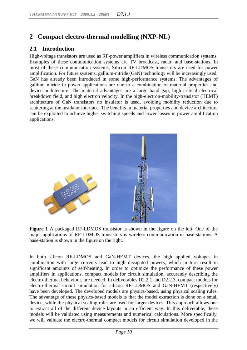
Figure 1 A packaged RF-LDMOS transistor is shown in the figure on the left. One of the
major applications of RF-LDMOS transistors is wireless communication in base-stations. A
base-station is shown in the figure on the right.
In both silicon RF-LDMOS and GaN-HEMT devices, the high applied voltages in
combination with large currents lead to high dissipated powers, which in turn result in
significant amounts of self-heating. In order to optimize the performance of these power
amplifiers in applications, compact models for circuit simulation, accurately describing the
electro-thermal behaviour, are needed. In deliverables D2.2.1 and D2.2.3, compact models for
electro-thermal circuit simulation for silicon RF-LDMOS and GaN-HEMT (respectively)
have been developed. The developed models are physics-based, using physical scaling rules.
The advantage of these physics-based models is that the model extraction is done on a small
device, while the physical scaling rules are used for larger devices. This approach allows one
to extract all of the different device layouts in an efficient way. In this deliverable, these
models will be validated using measurements and numerical calculations. More specifically,
we will validate the electro-thermal compact models for circuit simulation developed in the
THERMINATOR FP7 ICT – 2009.3.2 - 28603 D7.1.1
Page 11
Therminator deliverables D2.2.1 and D2.2.3 using pulsed and non-pulsed IV measurements in
Section 2.2.1. Furthermore, the integration of the electro-thermal models into the design flow
will be demonstrated, and validation on measurement data under application conditions will
be presented. In Section 2.2.2, the physical scaling of the thermal resistance in the compact
thermal models will be validated against numerical calculations using a Green’s function
method. The results of applying the S-parameter method to determine the thermal resistance
on different device types are given in Section 2.2.3. In this section, we apply the thermal
characterization to different device types not studied in the previous Therminator deliverables,
i.e. silicon-on-insulator (SOI) LDMOS and GaN Schottky diodes. The measurement results
are compared to the developed models.
2.2 Technical results
2.2.1 Validation of the thermal models for RF-LDMOS and GaN-HEMT with
measurements
The conventional approach in the development of electro-thermal compact models is to use a
combination of pulsed and DC IV measurements in the temperature range of interest. Both
pulsed and (non-pulsed) DC IV measurements are needed in order to be able to separate
electrical, temperature-dependent, and self-heating effects. The pulsed measurements are done
with pulses fast enough so that self-heating doesn’t occur. For the parameter extraction in the
compact model, the pulsed IV measurements are used to extract the electrical model
parameters. Subsequently, the temperature sensitivities of these electrical parameters are
obtained from the pulsed IV measurements at other temperatures. The final step is to fit the
thermal resistance, and its temperature dependence, on (non-pulsed) DC IV measurements at
different temperatures. Note that in this approach the thermal resistance is only a fitting
parameter in the model that accounts for the differences between pulsed and (non-pulsed) DC
IV measurements. Furthermore, there is no direct validation of the thermal resistance, since it
is not measured directly.
In order to measure the thermal resistance of a device directly, S-parameter measurements can
be used. Using this S-parameter measurement technique, pulsed IV measurements are also not
needed in the parameter extraction of the model. The thermal resistance is measured directly,
and can be set to the correct value in the compact model. The (non-pulsed) DC IV
characteristics at different temperatures are used to extract the electrical model parameters
and the corresponding temperature dependence. In Therminator deliverables D2.2.1 and
D2.2.3, this novel S-parameter technique for direct extraction of the thermal resistance was
applied to RF-LDMOS and GaN-HEMT power technologies. The thermal resistance was
characterized directly. These S-parameter measurements were used to set the thermal
resistance to the correct value in the corresponding compact models. Next, the model
parameters were extracted on the (non-pulsed) DC IV characteristics.
In this part of the deliverable, we will validate the models developed in deliverable D2.2.3
and D2.2.1 using pulsed and (non-pulsed) DC IV measurements over a wide range of
temperatures. Note that the pulsed IV measurements have not been used in the model
development and parameter extraction.
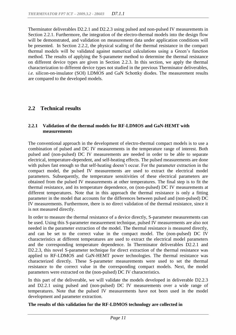
The results of this validation for the RF-LDMOS technology are collected in
THERMINATOR FP7 ICT – 2009.3.2 - 28603 D7.1.1
Page 12
Figure 2, Figure 3, and Figure 4. The measured pulsed and DC IDVDS characteristics of
an RF-LDMOS transistor at different temperatures are compared to the compact
electro-thermal model in
Figure 2. The pulsed measurements were done with a pulse width of 50 ns. It was
checked, by variation of the pulse width, that the applied pulses were fast enough such
that self-heating didn’t occur. Comparison of pulsed measurement data at different
temperatures shows that the amount of current decreases with increasing temperature
(see left column of
Figure 2), and the developed RF-LDMOS model correctly describes this temperature
dependence. In the right column of
Figure 2, the (non-pulsed) IDVDS characteristics are shown. These IV characteristics clearly
exhibit self-heating, as the current is smaller in comparison to pulsed IV characteristics, and
the current decreases with increasing bias. The developed model accurately describes the DC
IV measurement data.
Figure 2 IDVDS characteristics at VGS = 2.5, 3, 3.5, 4, 4.5, and 5 V of the RF-LDMOS device
measured at temperatures of T = 21 and 100 oC. The figures in the left column show the
pulsed IV characteristics, using a pulse width of 50 ns. The figures in the right column show
THERMINATOR FP7 ICT – 2009.3.2 - 28603 D7.1.1
Page 13
the DC IV characteristics. The scaling of the y-axis has been kept the same in all figures in
order to demonstrate the impact of the ambient temperature and self-heating on the device
characteristics. The measurements (red markers) and developed model (blue solid lines) are in
good agreement for the measured bias conditions and temperature range.
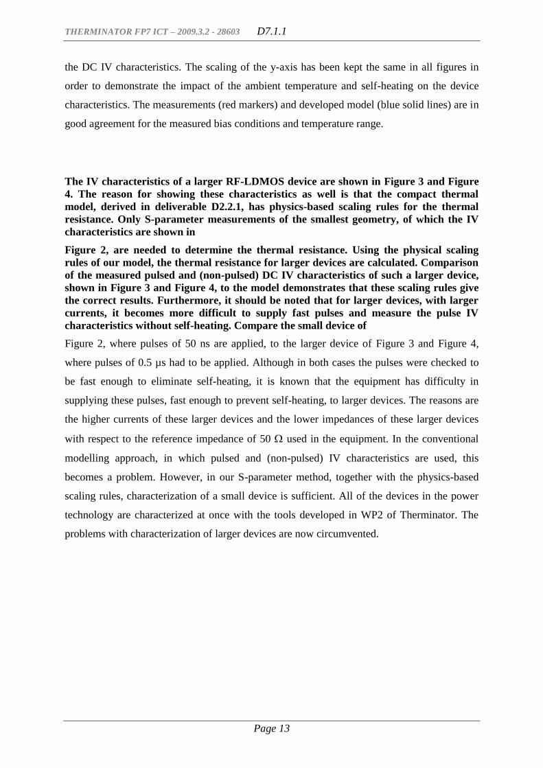
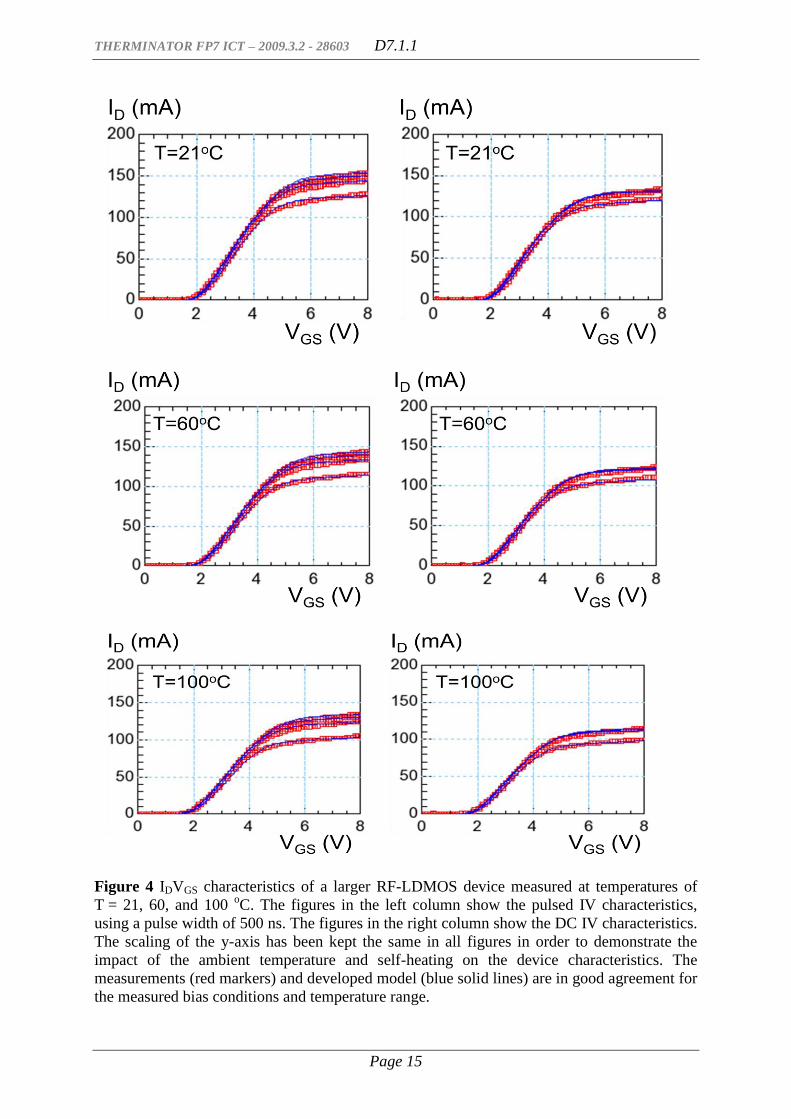
The IV characteristics of a larger RF-LDMOS device are shown in Figure 3 and Figure
4. The reason for showing these characteristics as well is that the compact thermal
model, derived in deliverable D2.2.1, has physics-based scaling rules for the thermal
resistance. Only S-parameter measurements of the smallest geometry, of which the IV
characteristics are shown in
Figure 2, are needed to determine the thermal resistance. Using the physical scaling
rules of our model, the thermal resistance for larger devices are calculated. Comparison
of the measured pulsed and (non-pulsed) DC IV characteristics of such a larger device,
shown in Figure 3 and Figure 4, to the model demonstrates that these scaling rules give
the correct results. Furthermore, it should be noted that for larger devices, with larger
currents, it becomes more difficult to supply fast pulses and measure the pulse IV
characteristics without self-heating. Compare the small device of
Figure 2, where pulses of 50 ns are applied, to the larger device of Figure 3 and Figure 4,
where pulses of 0.5 µs had to be applied. Although in both cases the pulses were checked to
be fast enough to eliminate self-heating, it is known that the equipment has difficulty in
supplying these pulses, fast enough to prevent self-heating, to larger devices. The reasons are
the higher currents of these larger devices and the lower impedances of these larger devices
with respect to the reference impedance of 50 used in the equipment. In the conventional
modelling approach, in which pulsed and (non-pulsed) IV characteristics are used, this
becomes a problem. However, in our S-parameter method, together with the physics-based
scaling rules, characterization of a small device is sufficient. All of the devices in the power
technology are characterized at once with the tools developed in WP2 of Therminator. The
problems with characterization of larger devices are now circumvented.
THERMINATOR FP7 ICT – 2009.3.2 - 28603 D7.1.1
Page 14
Figure 3 IDVDS characteristics of a larger RF-LDMOS device measured at temperatures of T
= 21, 60, and 100 oC. The figures in the left column show the pulsed IV characteristics, using
a pulse width of 500 ns. The figures in the right column show the DC IV characteristics. The
scaling of the y-axis has been kept the same in all figures in order to demonstrate the impact
of the ambient temperature and self-heating on the device characteristics. The measurements
(red markers) and developed model (blue solid lines) are in good agreement for the measured
bias conditions and temperature range.
THERMINATOR FP7 ICT – 2009.3.2 - 28603 D7.1.1
Page 15
Figure 4 IDVGS characteristics of a larger RF-LDMOS device measured at temperatures of
T = 21, 60, and 100 oC. The figures in the left column show the pulsed IV characteristics,
using a pulse width of 500 ns. The figures in the right column show the DC IV characteristics.
The scaling of the y-axis has been kept the same in all figures in order to demonstrate the
impact of the ambient temperature and self-heating on the device characteristics. The
measurements (red markers) and developed model (blue solid lines) are in good agreement for
the measured bias conditions and temperature range.
THERMINATOR FP7 ICT – 2009.3.2 - 28603 D7.1.1
Page 16
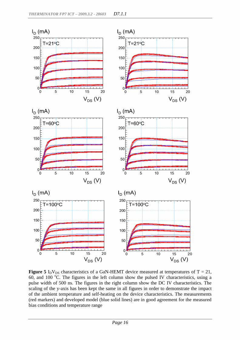
Figure 5 IDVDS characteristics of a GaN-HEMT device measured at temperatures of T = 21,
60, and 100 oC. The figures in the left column show the pulsed IV characteristics, using a
pulse width of 500 ns. The figures in the right column show the DC IV characteristics. The
scaling of the y-axis has been kept the same in all figures in order to demonstrate the impact
of the ambient temperature and self-heating on the device characteristics. The measurements
(red markers) and developed model (blue solid lines) are in good agreement for the measured
bias conditions and temperature range
THERMINATOR FP7 ICT – 2009.3.2 - 28603 D7.1.1
Page 17
Validation on the GaN-HEMT devices was done in the same way. A comparison of measured
pulsed and (non-pulsed) IV characteristics to the corresponding electro-thermal GaN-HEMT
model developed in Therminator deliverable D2.2.3 is shown in Figure 5. Measurements and
model were found to agree.
In summary, a detailed validation of the electro-thermal compact models for power
technologies developed in WP2 of Therminator on pulsed and non-pulsed IV-characteristics
has been presented (see
Figure 2–Figure 5) demonstrating our measurable objective MO7.1.1 of validation of thermal
models for RF-LDMOS and GaN-HEMT.
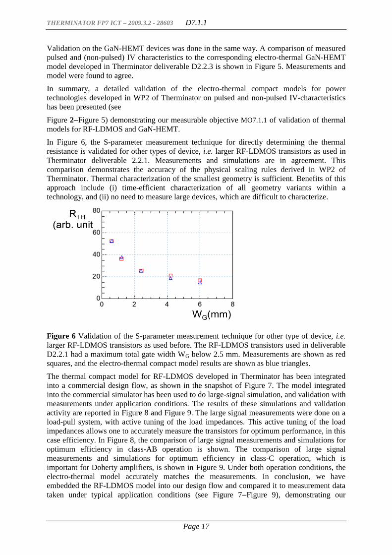
In Figure 6, the S-parameter measurement technique for directly determining the thermal
resistance is validated for other types of device, i.e. larger RF-LDMOS transistors as used in
Therminator deliverable 2.2.1. Measurements and simulations are in agreement. This
comparison demonstrates the accuracy of the physical scaling rules derived in WP2 of
Therminator. Thermal characterization of the smallest geometry is sufficient. Benefits of this
approach include (i) time-efficient characterization of all geometry variants within a
technology, and (ii) no need to measure large devices, which are difficult to characterize.
Figure 6 Validation of the S-parameter measurement technique for other type of device, i.e.
larger RF-LDMOS transistors as used before. The RF-LDMOS transistors used in deliverable
D2.2.1 had a maximum total gate width WG below 2.5 mm. Measurements are shown as red
squares, and the electro-thermal compact model results are shown as blue triangles.
The thermal compact model for RF-LDMOS developed in Therminator has been integrated
into a commercial design flow, as shown in the snapshot of Figure 7. The model integrated
into the commercial simulator has been used to do large-signal simulation, and validation with
measurements under application conditions. The results of these simulations and validation
activity are reported in Figure 8 and Figure 9. The large signal measurements were done on a
load-pull system, with active tuning of the load impedances. This active tuning of the load
impedances allows one to accurately measure the transistors for optimum performance, in this
case efficiency. In Figure 8, the comparison of large signal measurements and simulations for
optimum efficiency in class-AB operation is shown. The comparison of large signal
measurements and simulations for optimum efficiency in class-C operation, which is
important for Doherty amplifiers, is shown in Figure 9. Under both operation conditions, the
electro-thermal model accurately matches the measurements. In conclusion, we have
embedded the RF-LDMOS model into our design flow and compared it to measurement data
taken under typical application conditions (see Figure 7–Figure 9), demonstrating our

THERMINATOR FP7 ICT – 2009.3.2 - 28603 D7.1.1
Page 18
measurable objective MO7.1.3 of integration of the electro-thermal model for RF-LDMOS
into design tools and validation on large-signal application data.
Figure 7 Schematic representation of the electro-thermal RF-LDMOS model in a commercial
design tool, i.e. the Agilent ADS simulator. The nodes T1 and T2 are the nodes of the thermal
compact model derived in Therminator deliverable D2.2.1.
Figure 8 Large-signal validation in class-AB operation of the RF-LDMOS model. The power
gain (GP), transducer gain (GT), and efficiency are shown as a function of the output power.
The red markers and green line correspond to the measured and simulated power gain (GP),
whereas the light blue markers and dark blue line correspond to the measured and simulated
transducer gain (GT), both displayed on the left y-axis. The grey markers and black line
correspond to the measured and simulated efficiency, displayed on the right y-axis.
THERMINATOR FP7 ICT – 2009.3.2 - 28603 D7.1.1
Page 19
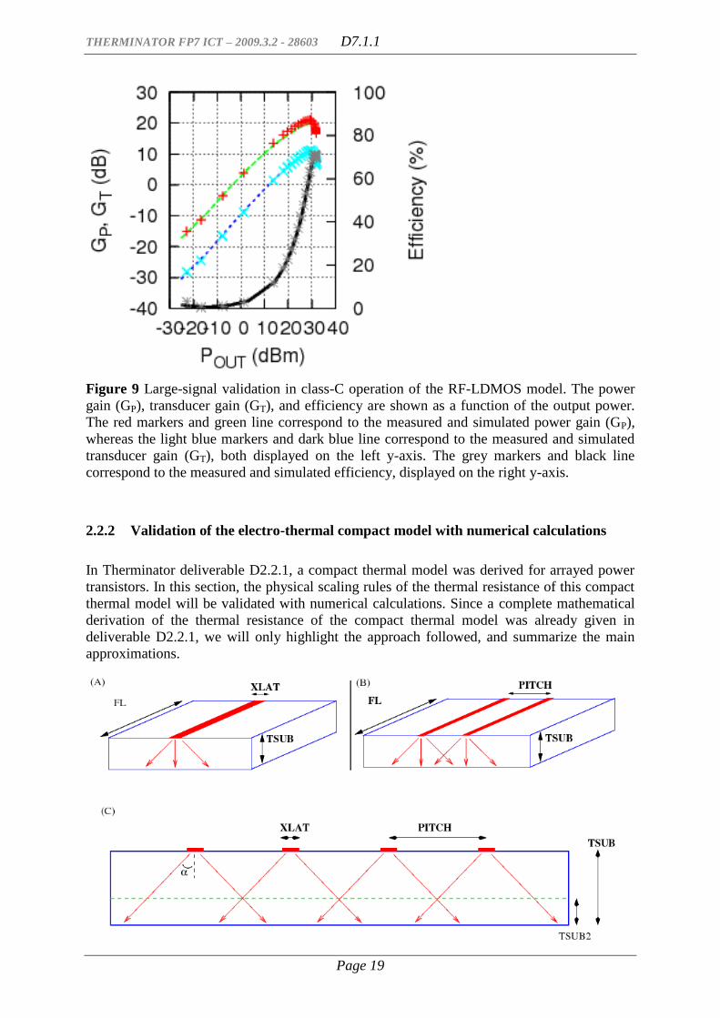
Figure 9 Large-signal validation in class-C operation of the RF-LDMOS model. The power
gain (GP), transducer gain (GT), and efficiency are shown as a function of the output power.
The red markers and green line correspond to the measured and simulated power gain (GP),
whereas the light blue markers and dark blue line correspond to the measured and simulated
transducer gain (GT), both displayed on the left y-axis. The grey markers and black line
correspond to the measured and simulated efficiency, displayed on the right y-axis.
2.2.2 Validation of the electro-thermal compact model with numerical calculations
In Therminator deliverable D2.2.1, a compact thermal model was derived for arrayed power
transistors. In this section, the physical scaling rules of the thermal resistance of this compact
thermal model will be validated with numerical calculations. Since a complete mathematical
derivation of the thermal resistance of the compact thermal model was already given in
deliverable D2.2.1, we will only highlight the approach followed, and summarize the main
approximations.
THERMINATOR FP7 ICT – 2009.3.2 - 28603 D7.1.1
Page 20
Figure 10 A power device with finger length FL and lateral dimensions XLAT is represented
by a heat source at the surface of the substrate shown in figure A. In practice, multiple devices
are organized in arrays, and thermal cross-talk or mutual heating will occur, as shown as in
figure B. A compact thermal model for transistors, separated by a distance PITCH in an array,
was derived in Therminator deliverable D2.2.1 by assuming that the heat flows within an
angle into the substrate. In the upper layer of the substrate, no mutual heating occurs,
whereas in the bottom layer the heat conduction is proportional to the total area of the array
(see figure C).
In a power device, the heat is generated at the surface of the substrate, where the current is
transported. For a single transistor, the heat is generated in a rectangular area. The dimensions
of this area are the finger length FL and the lateral dimension of current flow XLAT. The
finger length is the width of the device. XLAT corresponds to the distance from the source to
the drain. Since the finger length (~0.1–1 mm) is much longer than the lateral dimension
(~2–5 µm), thermal effects at the end of the finger were neglected in the compact thermal
model. For this reason, the heat source of a single transistor was modelled as a uniform strip,
as shown in Figure 10A. In practical devices, multiple transistors are arranged in arrays (see
Figure 10B), and thermal cross-talk or mutual heating will occur. In the compact thermal
model, it was assumed that the heat flows within an angle into the substrate, as shown in
Figure 10C. The thermal resistance of the arrayed devices was calculated in the compact
thermal model by assuming that (i) no mutual heating in the top layer of the substrate occurs,
and (ii) the heat conduction is proportional to the area of the total array in the bottom layer of
the substrate (see Figure 10C). With the aforementioned approximations, it was demonstrated
in deliverable D2.2.1 that it is possible to derive an analytical expression for the thermal
resistance depending on all relevant geometry variables for power technologies, i.e. finger
length, lateral device dimension, pitch, and substrate thickness.
In order to validate the compact thermal model, numerical calculations of the thermal
resistance were done using an in-house software tool. These numerical calculations are based
on directly solving the heat equation using a Green’s function approach. This numerical
approach is of course too time-consuming to be integrated within a compact device model of
the transistor for fast circuit simulations. However, directly comparing the results of these
numerical calculations using the Green’s function approach to the derived compact thermal
model for different layout variations is possible. The main results of this comparison are
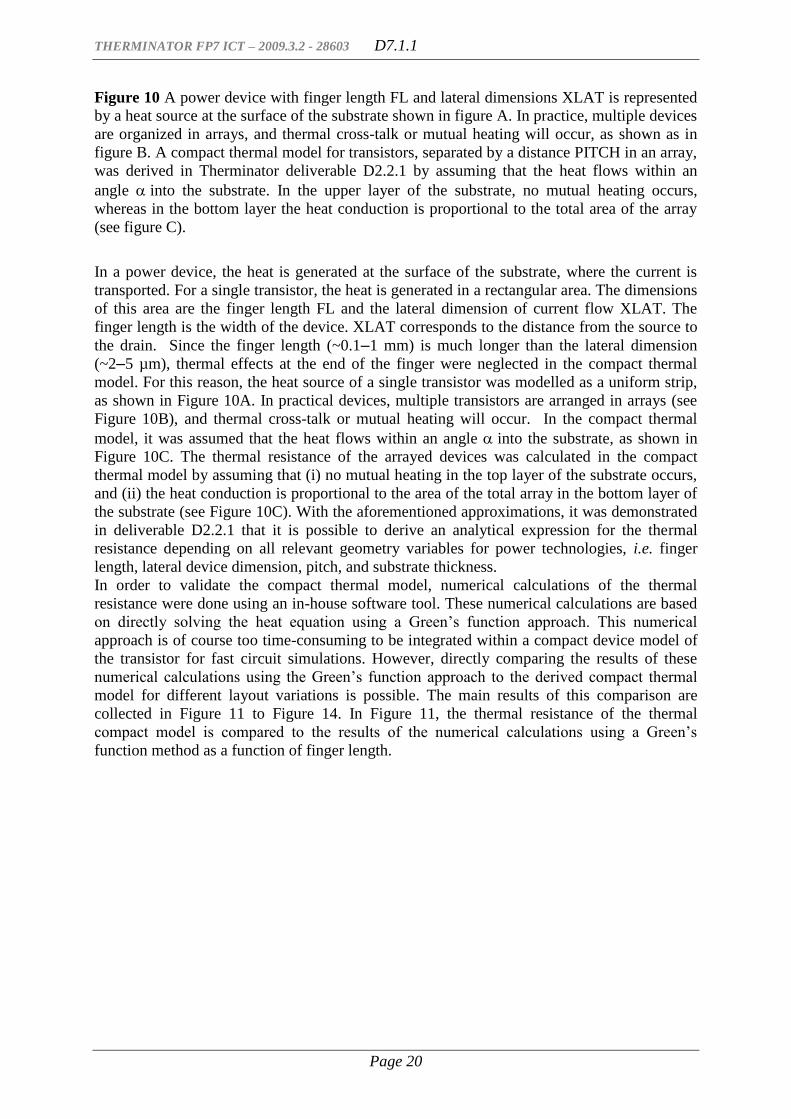
collected in Figure 11 to Figure 14. In Figure 11, the thermal resistance of the thermal
compact model is compared to the results of the numerical calculations using a Green’s
function method as a function of finger length.
THERMINATOR FP7 ICT – 2009.3.2 - 28603 D7.1.1
Page 21
Figure 11 Validation of the thermal compact model (blue markers) with numerical
calculations using a Green’s function method (solid red line). The thermal resistance is
shown as a function of finger length FL for a single-cell device, 3 devices, and 5 devices in
parallel.
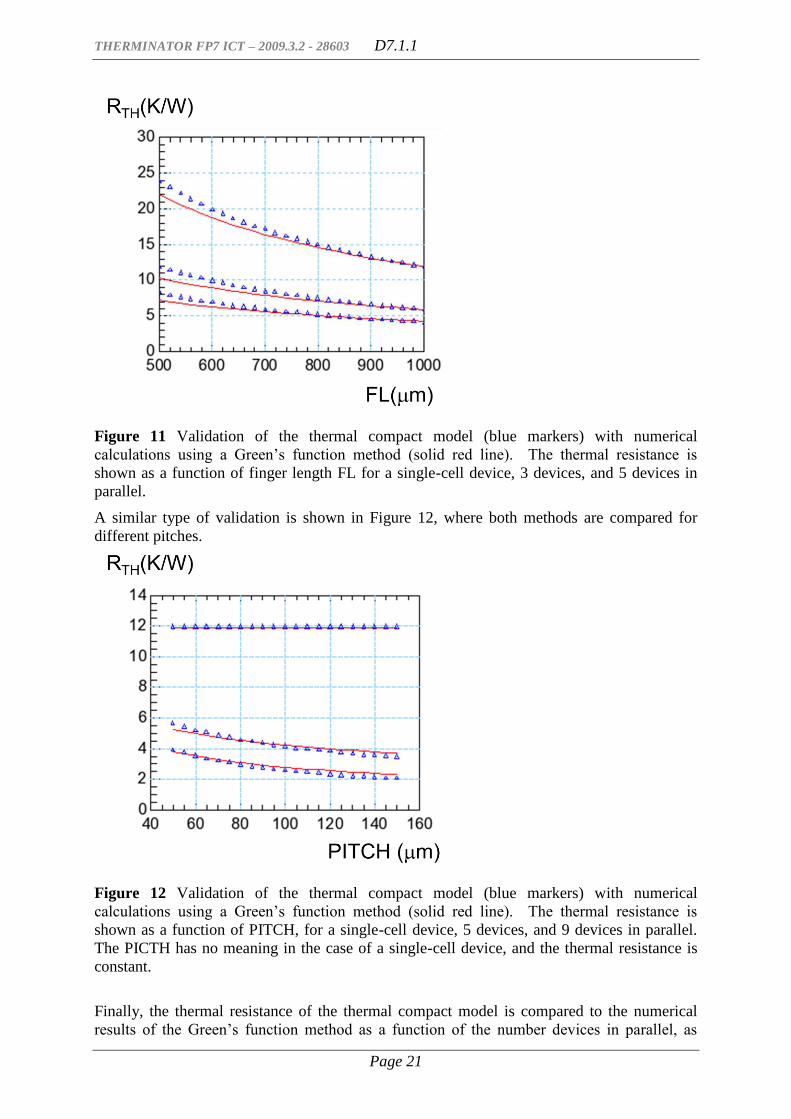
A similar type of validation is shown in Figure 12, where both methods are compared for
different pitches.
Figure 12 Validation of the thermal compact model (blue markers) with numerical
calculations using a Green’s function method (solid red line). The thermal resistance is
shown as a function of PITCH, for a single-cell device, 5 devices, and 9 devices in parallel.
The PICTH has no meaning in the case of a single-cell device, and the thermal resistance is
constant.
Finally, the thermal resistance of the thermal compact model is compared to the numerical
results of the Green’s function method as a function of the number devices in parallel, as

THERMINATOR FP7 ICT – 2009.3.2 - 28603 D7.1.1
Page 22
shown in Figure 13, and Figure 14. In summary, Figure 11–Figure 14 demonstrate that the
approximations made in the thermal compact model are validated by the numerical
calculations using the Green’s function method for all the relevant geometry variations in a
power technology.
Figure 13 Validation of the thermal compact model (blue markers) with numerical
calculations using a Green’s function method (red markers). The thermal resistance is shown
as a function of the number of cells for PITCHES of 50, 100, and 150 µm.
Figure 14 Validation of the thermal compact model (blue markers) with numerical
calculations using a Green’s function method (red markers). The thermal resistance is shown
as a function of the number of cells for PITCHES of 50, 100, and 150 µm.
2.2.3 Validation on different types of device
In this section, the S-parameter method for determining the thermal resistance is applied to
different device types not studied in the previous Therminator deliverables (D2.2.1 and
D2.2.3). For the silicon devices, silicon-on-insulator (SOI) LDMOS devices are studied

THERMINATOR FP7 ICT – 2009.3.2 - 28603 D7.1.1
Page 23
instead of the RF-LDMOS devices. For GaN devices, Schottky diodes instead of GaN
HEMTs are measured and validated with a model.
The basic working principle of the physics-based electro-thermal compact model is shown in
Figure 15. The total dissipated power in the device, Pdiss, is calculated from the compact
model describing the electrical characteristics of the device. The thermal network calculates
the temperature increase with respect to the ambient temperature using the dissipated power.
The calculated temperature increase results in a different parameter set for the compact model
of the device, which in turn results in a different amount of dissipated power. The final
transistor temperature and dissipated power are known after the compact device model and
thermal model have converged in the circuit simulator.
Figure 15 Schematic overview of the working principle of a device compact model in
combination with a thermal model. For modelling the GaN Schottky diode, the device
compact model of the GaN HEMT, developed in deliverable D2.2.3, will be replaced by a
developed GaN Schottky diode model. For modelling the SOI-LDMOS, the thermal model
for RF-LDMOS, developed in deliverable D2.2.1, will be adapted for SOI.
To study and compare measurements with models for the different device types, appropriate
changes need to be made in existing models developed in WP2 of Therminator. These
changes can be in the device compact model and/or in thermal model of Figure 15. In order to
study the GaN Schottky diodes, the GaN-HEMT compact device model as developed in
D2.2.3 needs to be replaced by a Schottky diode model. The thermal model can be reused,
because the Schottky diodes are organized in arrays in the same way as the RF-power devices
(see Figure 10). For SOI-LDMOS, the silicon RF-LDMOS model approach can be used as a
starting point. In this case, the main modifications are in thermal model where the different
substrate, i.e. oxide instead of silicon, requires adaptation.

THERMINATOR FP7 ICT – 2009.3.2 - 28603 D7.1.1
Page 24
2.2.3.1 GaN Schottky diodes
A schematic cross-section of the GaN Schottky diode is shown in Figure 16. The material
layers on top of the substrate are the main GaN layer and an AlGaN layer. A thin layer of
electrons, i.e. a two-dimensional electron gas (2DEG), is formed at the AlGaN-GaN hetero-
junction, i.e. the interface between the AlGaN and GaN layers. The anode makes a Schottky
contact to the 2DEG layer, whereas the cathode contact of the diode is made by a metal with
an Ohmic contact to the 2DEG layer.
Figure 16 Schematic cross-section of the GaN Schottky diode (left), and schematic band
diagram (right), showing the Fermi level (EF) and the conduction-band minimum (EC) at
equilibrium.
In order to characterize the GaN Schottky diode, the S-parameter characterization technique
(as described as part of Therminator deliverable D1.1.1) is used. The S-parameter technique
allows one to determine the thermal resistance directly from measurements. The measurement
results are compared to the developed electro-thermal compact model for the Schottky diodes.
The model parameters have been extracted on the measurements of the smallest device only.
The physical scaling rules have been used to compute the thermal resistances for the larger
devices with more devices in parallel, different finger length, and variations in device
separation (pitch).
The thermal resistance of the Schottky diode as measured with the S-parameter
characterization technique is compared to the developed Schottky model in Figure 17. The
thermal resistance was extracted under forward operation of the diode. Measurements and

THERMINATOR FP7 ICT – 2009.3.2 - 28603 D7.1.1
Page 25
model were found to be in good agreement over the measured temperature range from 20 oC
to 90 oC.
Figure 17 Thermal resistance RTH versus ambient temperature Tamb, comparing direct
characterization of the thermal resistance using S-parameters (red rectangles) to the Schottky
diode model (blue line).
The thermal resistance as a function of finger length FL is shown in Figure 18. In the compact
thermal model derived for GaN-HEMT in deliverable D2.2.3 of Therminator WP2, and now
reused for the GaN Schottky diodes, thermal effects at the edges of the fingers were assumed
to be small enough to be neglected. From symmetry it follows that the resulting thermal
resistance has to be inversely proportional to the finger length FL. The measurements, as
shown in Figure 18, demonstrate this dependence.
Figure 18 Thermal resistance times finger length (RTH × FL) versus the finger length (FL),
comparing direct characterization using S-parameters (red rectangles) to our Schottky diode
model (blue triangles). The measurements demonstrate that the thermal resistance of the
THERMINATOR FP7 ICT – 2009.3.2 - 28603 D7.1.1
Page 26
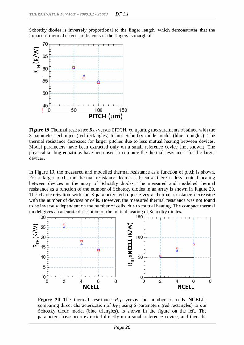
Schottky diodes is inversely proportional to the finger length, which demonstrates that the
impact of thermal effects at the ends of the fingers is marginal.
Figure 19 Thermal resistance RTH versus PITCH, comparing measurements obtained with the
S-parameter technique (red rectangles) to our Schottky diode model (blue triangles). The
thermal resistance decreases for larger pitches due to less mutual heating between devices.
Model parameters have been extracted only on a small reference device (not shown). The
physical scaling equations have been used to compute the thermal resistances for the larger
devices.
In Figure 19, the measured and modelled thermal resistance as a function of pitch is shown.
For a larger pitch, the thermal resistance decreases because there is less mutual heating
between devices in the array of Schottky diodes. The measured and modelled thermal
resistance as a function of the number of Schottky diodes in an array is shown in Figure 20.
The characterization with the S-parameter technique gives a thermal resistance decreasing
with the number of devices or cells. However, the measured thermal resistance was not found
to be inversely dependent on the number of cells, due to mutual heating. The compact thermal
model gives an accurate description of the mutual heating of Schottky diodes.
Figure 20 The thermal resistance RTH versus the number of cells NCELL,
comparing direct characterization of RTH using S-parameters (red rectangles) to our
Schottky diode model (blue triangles), is shown in the figure on the left. The
parameters have been extracted directly on a small reference device, and then the
THERMINATOR FP7 ICT – 2009.3.2 - 28603 D7.1.1
Page 27
physical scaling equations have been used in order to obtain the thermal parameters
for the other devices. In the figure on the right, the same thermal resistance data has
been scaled with NCELL. In the absence of mutual heating between cells, this scaled
thermal resistance should be constant, as shown by the solid black line. However, the
scaled thermal resistance obtained from direct characterization (red rectangles) is not
constant due to mutual heating. The derived compact thermal model with mutual
heating and its physical scaling (blue triangles) is in good agreement with the
measurements.
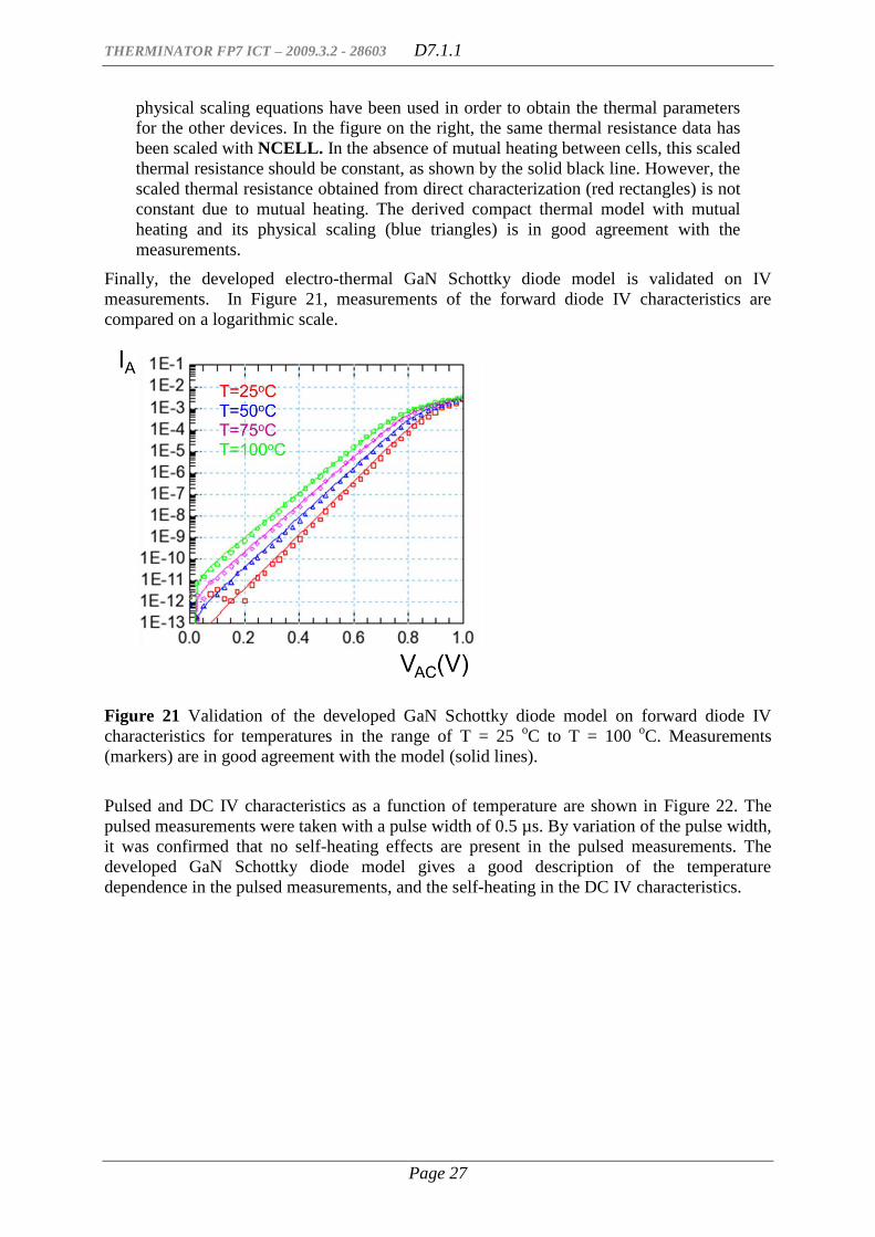
Finally, the developed electro-thermal GaN Schottky diode model is validated on IV
measurements. In Figure 21, measurements of the forward diode IV characteristics are
compared on a logarithmic scale.
Figure 21 Validation of the developed GaN Schottky diode model on forward diode IV
characteristics for temperatures in the range of T = 25 oC to T = 100
oC. Measurements
(markers) are in good agreement with the model (solid lines).
Pulsed and DC IV characteristics as a function of temperature are shown in Figure 22. The
pulsed measurements were taken with a pulse width of 0.5 µs. By variation of the pulse width,
it was confirmed that no self-heating effects are present in the pulsed measurements. The
developed GaN Schottky diode model gives a good description of the temperature
dependence in the pulsed measurements, and the self-heating in the DC IV characteristics.

THERMINATOR FP7 ICT – 2009.3.2 - 28603 D7.1.1
Page 28
Figure 22 Validation of the developed GaN Schottky diode model on pulsed IV
measurements in the figure on the left, and DC IV measurements in the figure on the right.
Measurements (markers) are in good agreement with the model for measured temperatures in
the range of T = 25 oC to T = 100
oC.
Figure 23 shows a detail of the forward Schottky diode IV characteristics with a temperature
inversion point. The temperature inversion point exists because at low forward voltages VAC
the current increases with temperature, as shown in Figure 21, whereas at higher forward
voltages VAC the current decreases with temperature. At lower forward voltages, the current
increases with temperature because of the diode characteristics (I ~ exp(VAC/(kB·T))). The
decrease of current at higher forward voltages occurs because the series resistance of the
2DEG increases with temperature.
Figure 23 Detail of the forward Schottky diode IV characteristics. The measurements show a
temperature inversion point around a forward voltage VAC = 1.1 V. The temperature inversion
is the result of diode IV characteristics, which increase with temperature at low forward
voltages (see also Figure 21), and decrease with temperature due to an increasing series
THERMINATOR FP7 ICT – 2009.3.2 - 28603 D7.1.1
Page 29
resistance. The temperature inversion effect in the measured IV characteristics (markers) is
described accurately by our GaN Schottky diode model.
The overall accuracy of the GaN Schottky diode model, as shown in Figure 17–Figure 23,
was found to be within 15%.
2.2.3.2 SOI-LDMOS
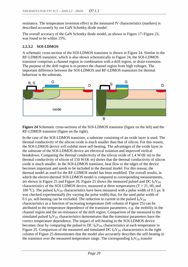
A schematic cross-section of the SOI-LDMOS transistor is shown in Figure 24. Similar to the
RF-LDMOS transistor, which is also shown schematically in Figure 24, the SOI-LDMOS
transistor comprises a channel region in combination with a drift region, or drain extension.
The purpose of the drift region is to protect the channel region from high voltages. The
important difference between the SOI-LDMOS and RF-LDMOS transistors for thermal
behaviour is the substrate.
Figure 24 Schematic cross-sections of the SOI-LDMOS transistor (figure on the left) and the
RF-LDMOS transistor (figure on the right).
In the case of the SOI-LDMOS transistor, a substrate consisting of an oxide layer is used. The
thermal conductivity of the silicon oxide is much smaller than that of silicon. For this reason,
the SOI-LDMOS device will exhibit more self-heating. The advantages of the oxide layer in
the substrate of the SOI-LDMOS device are electrical isolation and improved vertical
breakdown. Comparing the thermal conductivity of the silicon oxide of 1.4 W/(K·m) to the
thermal conductivity of silicon of 150 W/(K·m) shows that the thermal conductivity of silicon
oxide is much smaller. In the SOI-LDMOS transistor, heat flow to the edges of the device
becomes important and needs to be included in the thermal model. For this reason, the
thermal model as used for the RF-LDMOS model has been modified. The overall results, in
which the electro-thermal SOI-LDMOS model is compared to corresponding measurements,
are shown in Figure 25 and Figure 26. Figure 25 shows the measured pulsed and DC IDVDS
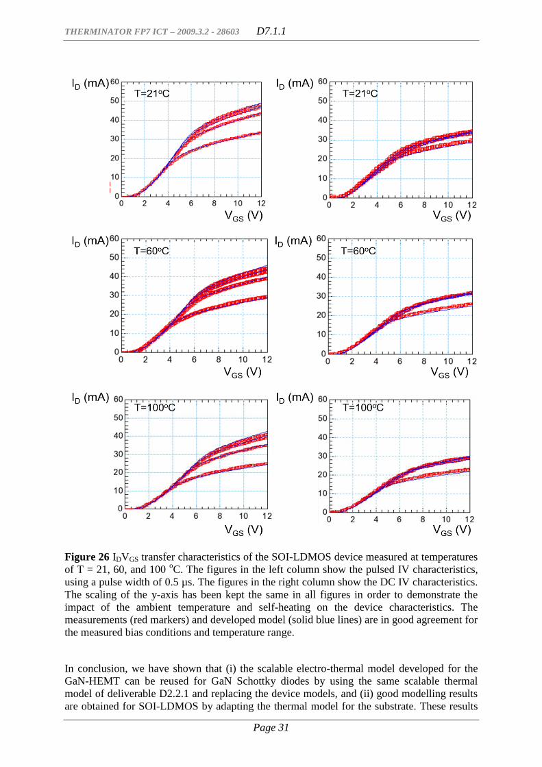
characteristics of the SOI-LDMOS device, measured at three temperatures (T = 21, 60, and
100 oC). The pulsed IDVDS characteristics have been measured with a pulse width of 0.5 µs. It
was checked experimentally (by varying the pulse width) that, for the used pulse width of
0.5 µs, self-heating can be excluded. The reduction in current in the pulsed IDVDS
characteristics as a function of increasing temperature (left column of Figure 25) can be
attributed to the temperature dependence of the transistor parameters, e.g. the mobility in the
channel region and the on-resistance of the drift region. Comparison of the measured to the
simulated pulsed IDVDS characteristics demonstrates that the transistor parameters have the
correct temperature dependence. The impact of self-heating in the SOI-LDMOS device
becomes clear by comparing the pulsed to DC IDVDS characteristics at each temperature in
Figure 25. Comparison of the measured and simulated DC IDVDS characteristics in the right
column of Figure 25 demonstrates that the model also accurately describes the self-heating in
the transistor over the measured temperature range. The corresponding IDVGS transfer

THERMINATOR FP7 ICT – 2009.3.2 - 28603 D7.1.1
Page 30
characteristics are shown in Figure 26. The accuracy of the electro-thermal SOI-LDMOS
model, shown in Figure 25 and Figure 26, was found to be within 15%.
Figure 25 IDVDS characteristics of the SOI-LDMOS device measured at temperatures of
T = 21, 60, and 100 oC. The figures in the left column show the pulsed IV characteristics,
using a pulse width of 0.5 µs. The figures in the right column show the DC IV characteristics.
The scaling of the y-axis has been kept the same in all figures in order to demonstrate the
impact of the ambient temperature and self-heating on the device characteristics. The
measurements (red markers) and developed model (solid blue lines) are in good agreement for
the measured bias conditions and temperature range.
THERMINATOR FP7 ICT – 2009.3.2 - 28603 D7.1.1
Page 31
Figure 26 IDVGS transfer characteristics of the SOI-LDMOS device measured at temperatures
of T = 21, 60, and 100 oC. The figures in the left column show the pulsed IV characteristics,
using a pulse width of 0.5 µs. The figures in the right column show the DC IV characteristics.
The scaling of the y-axis has been kept the same in all figures in order to demonstrate the
impact of the ambient temperature and self-heating on the device characteristics. The
measurements (red markers) and developed model (solid blue lines) are in good agreement for
the measured bias conditions and temperature range.
In conclusion, we have shown that (i) the scalable electro-thermal model developed for the
GaN-HEMT can be reused for GaN Schottky diodes by using the same scalable thermal
model of deliverable D2.2.1 and replacing the device models, and (ii) good modelling results
are obtained for SOI-LDMOS by adapting the thermal model for the substrate. These results
THERMINATOR FP7 ICT – 2009.3.2 - 28603 D7.1.1
Page 32
demonstrate our measurable objective MO7.1.2 of reuse by adapting electro-thermal models
developed on RF power technologies for other types of devices.
2.3 Conclusions
Compact electro-thermal models for silicon RF-LDMOS and GaN-HEMT devices have been
developed in WP2 of Therminator (deliverable D2.2.1 and D2.2.3). These models derived in
WP2 are physics-based and have a scalable model for the thermal resistance. In this
deliverable, these models have been validated using measurements and numerical
calculations. The validation against measurement data has demonstrated that the compact
models give an accurate description of the pulsed and DC IV characteristics over a wide
temperature range for both silicon RF-LDMOS and GaN-HEMT. In addition, the models have
been shown to be in good agreement with large-signal application measurements. Next, the
thermal compact model has been compared to numerical calculations using a Green’s function
approach. This comparison has resulted in validation of the approximations made in the
derivation of the compact thermal model in WP2, as well as validation of the compact thermal
model over a wide range of geometries.
Furthermore, the developed models have been validated on different device types, i.e. larger
geometries as used in WP2 for RF-LDMOS and other device types. The other device types
are SOI-LDMOS and GaN Schottky diodes. The S-parameter method for determining the
thermal resistance has been used to characterize the thermal device properties. By making the
appropriate changes in the device or thermal models in the models for the RF-power devices
developed in WP2, accurate modelling of the SOI-LDMOS and GaN Schottky diodes was
demonstrated.
In conclusion, the measurable objective MO7.1.1 of validation of the thermal RF-
LDMOS and GaN-HEMT models has been demonstrated in Section 2.2.1 (
Figure 2–Figure 5). The measurable objective MO7.1.2 of reusing and adapting the electro-
thermal models developed for RF-devices on other device types has been shown in Section
2.2.3 (Figure 17–Figure 23 and Figure 25–Figure 26), and the integration of the RF-LDMOS
model into design tools and validation on large-signal application data (MO7.1.3) was
demonstrated in Section 2.2.1 (Figure 7–Figure 9).
THERMINATOR FP7 ICT – 2009.3.2 - 28603 D7.1.1
Page 33
3 Verification of TCAD
(SNPS-CH, together with IMC, IMEC, ST, NXP-D)
3.1 Introduction
This section reports about the verification of Technology CAD (TCAD) calibrated simulation
decks that were developed in WP2 and WP6 by SNPS-CH with and for supporting different
partners for studying thermal effects at the very low end of the abstraction hierarchy.
The model details are described in the respective WP2 and WP6 deliverable reports.
TCAD simulation includes is the modelling of process steps (such as diffusion and ion
implantation), and modelling of the electro-thermal behaviour of the devices based on
fundamental physics, such as the doping profiles of the devices.
TCAD enables in-depth analysis of device behaviour, i.e. self-heating, that is relevant to
modelling at higher levels of abstraction by running virtual experiments, and allows
separation of physical effects that would not be possible with measurements only.
3.2 Verification of TCAD Models and Methodologies
3.2.1 Bulk CMOS 3D TCAD Model
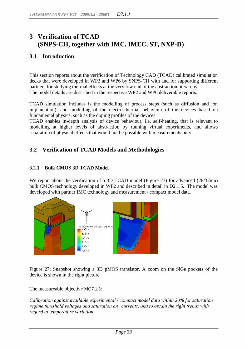
We report about the verification of a 3D TCAD model (Figure 27) for advanced (28/32nm)
bulk CMOS technology developed in WP2 and described in detail in D2.1.5. The model was
developed with partner IMC technology and measurement / compact model data.
Measurable objectives:
Figure 27: Snapshot showing a 3D pMOS transistor. A zoom on the SiGe pockets of the
device is shown in the right picture.
The measureable objective MO7.1.5:
Calibration against available experimental / compact model data within 20% for saturation
regime threshold voltages and saturation on−currents, and to obtain the right trends with
regard to temperature variation.

THERMINATOR FP7 ICT – 2009.3.2 - 28603 D7.1.1
Page 34
was fully achieved for NMOS (10%), whereas for PMOS the accuracy achieved was Vtsat
within 30%, Ion within 35%. However, for both NMOS and PMOS cases the Vtsat
temperature trend (deltaVtsat/deltaT) is captured with an accuracy of better than 20%. In
order to improve the PMOS absolute accuracy, more detailed process flow and geometry
description need to be available. However, because of IMCs data and IP protection
requirements neither device geometry information nor process flow description was available
for this implementation.
This is shown in Figure 28 and Figure 29 for the saturation on-currents, and in Figure 30 for
the saturation regime threshold voltage Vtsat.
Figure 28: Comparison of the nMOS IdVg in saturation regime of the 3D TCAD model (left)
with the data extracted from the compact model provided by IMC (right). The device
geometry is L/W=33nm/80nm. The saturation on-currents agree within 10% over the
temperature range from -40deg.C up to 125deg.C.
Figure 29: Comparison of the pMOS IdVg in saturation regime of the 3D TCAD model (left)
with the data extracted from the compact model provided by IMC (right). The device
geometry is L/W=33nm/80nm. The saturation on-currents agree only within 35% over the
temperature range from -40deg.C up to 125deg.C. In particular, the crossing point at Vg = -
1.2V is not well captured in the TCAD model.
THERMINATOR FP7 ICT – 2009.3.2 - 28603 D7.1.1
Page 35
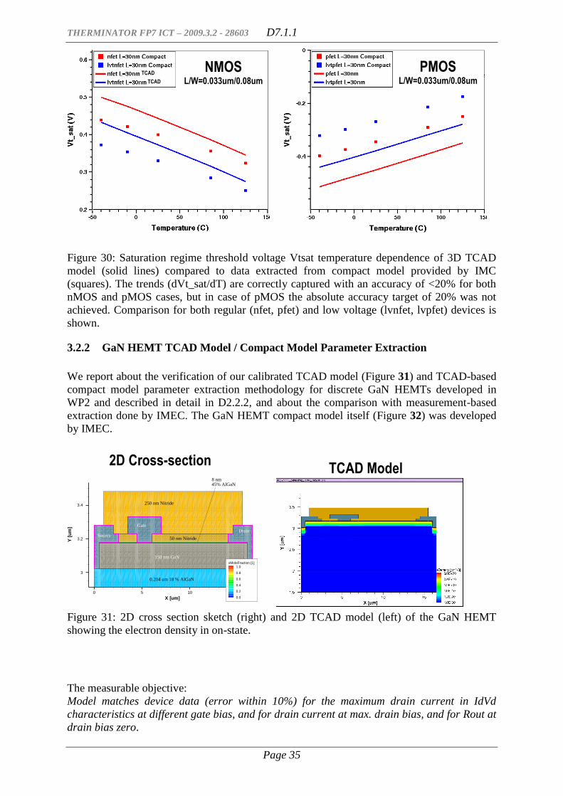
Figure 30: Saturation regime threshold voltage Vtsat temperature dependence of 3D TCAD
model (solid lines) compared to data extracted from compact model provided by IMC
(squares). The trends (dVt_sat/dT) are correctly captured with an accuracy of <20% for both
nMOS and pMOS cases, but in case of pMOS the absolute accuracy target of 20% was not
achieved. Comparison for both regular (nfet, pfet) and low voltage (lvnfet, lvpfet) devices is
shown.
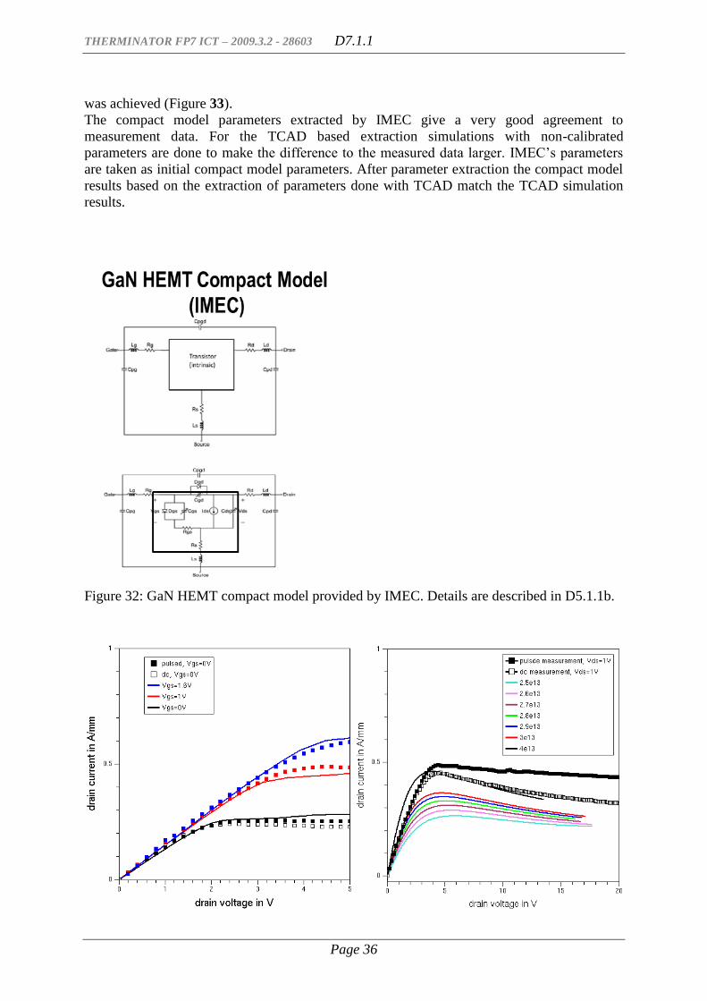
3.2.2 GaN HEMT TCAD Model / Compact Model Parameter Extraction
We report about the verification of our calibrated TCAD model (Figure 31) and TCAD-based
compact model parameter extraction methodology for discrete GaN HEMTs developed in
WP2 and described in detail in D2.2.2, and about the comparison with measurement-based
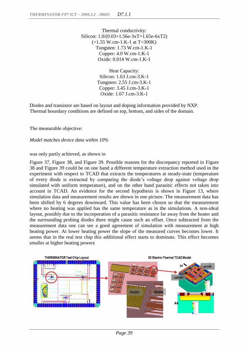
extraction done by IMEC. The GaN HEMT compact model itself (Figure 32) was developed
by IMEC.
Figure 31: 2D cross section sketch (right) and 2D TCAD model (left) of the GaN HEMT
showing the electron density in on-state.
The measurable objective:
Model matches device data (error within 10%) for the maximum drain current in IdVd
characteristics at different gate bias, and for drain current at max. drain bias, and for Rout at
drain bias zero.
X [um]
Y[u
m]
0 5 10 15
3
3.2
3.4
xMoleFraction [1]
1.0
0.8
0.6
0.4
0.2
0.0
0.204 um 18 % AlGaN
150 nm GaN
250 nm Nitride
50 nm Nitride
8 nm45% AlGaN
DrainGate
Source
TCAD TCAD
NMOS L/W=0.033um/0.08um
PMOS L/W=0.033um/0.08um
TCAD Model 2D Cross-section
THERMINATOR FP7 ICT – 2009.3.2 - 28603 D7.1.1
Page 36
was achieved (Figure 33).
The compact model parameters extracted by IMEC give a very good agreement to
measurement data. For the TCAD based extraction simulations with non-calibrated
parameters are done to make the difference to the measured data larger. IMEC’s parameters
are taken as initial compact model parameters. After parameter extraction the compact model
results based on the extraction of parameters done with TCAD match the TCAD simulation
results.
Figure 32: GaN HEMT compact model provided by IMEC. Details are described in D5.1.1b.

THERMINATOR FP7 ICT – 2009.3.2 - 28603 D7.1.1
Page 37
Figure 33: TCAD model IdVd simulation results compared to measurement data provided by
IMEC. The figure on the right shows the effect of self-heating (negative differential
resistance) for Vgs=1V, and the effect of different AlGaN/GaN interface trap densities. Solid
lines = TCAD, Symbols = measurement.
Figure 34: IdVd characteristics comparison. Vgs=1.6V.
3.2.3 Si power MOSFET unit cell TCAD Model
We report about the discrete power MOSFET TCAD unit cell model verification. The model
was developed in WP2 with partner ST and its details are presented in D2.2.2.
The measurable objective MO7.1.4:
Model matches device data (error within 10%) for the maximum drain current in IdVd
characteristics at different gate bias, and for drain current at max. drain bias, and for Rout at
drain bias zero.
was essentially achieved.
Rout matches the reference data from ST mostly within an error < 10% in IdVd
characteristics at different gate bias and temperatures (Figure 35). Only at Vgs=10V and at
the low temperatures boundary we were not able to meet the objective (<15%). In accordance
TCAD
Compact Model IdVd with initial parameters from
IMEC
TCAD
Compact Model IdVd with optimized parameters based on TCAD

THERMINATOR FP7 ICT – 2009.3.2 - 28603 D7.1.1
Page 38
with partner ST we preferred to preserve predictability and consistency over the Vgs and
temperature range, rather than do a “brute force” fitting to measurements.
The maximum drain current (Ids) objective was not applied to the power MOSFET TCAD
model. The bias conditions for Ids@Vds=20V would correspond to an operating point well
beyond static (and dynamic) safe operating area (SOA) for all Vgs>3V.
Figure 35 Top: 2D TCAD model of the power MOSFET unit cell.
Bottom: Measured (_m) vs. Simulated (_s) Rdson at two different Ids current values
(Ids=10A, 80A) for Vgs=4.5V (left) and Vgs=10V (right), and temperatures -50C, 0C, 25C,
100C, 175C. Rdson (Rout) increases with temperature. The Inset shows the accuracy of
TCAD with respect to measurement.
3.2.4 3D TCAD Electro-Thermal Modeling Methodology
We report about the verification of the electro-thermal 3D TCAD Modeling Methodology for
discrete devices developed in WP6 with partner NXP-D. The model details are presented in
the deliverable report D6.1.1. The verification is performed against NXP test chip (
Figure 36) measurement data. We are focusing on the bipolar structure on the test chip
(encircled red). The aim of the test structure is the monitoring of the silicon temperature by
using sense diodes (“horizontal”: h1,h2,h3,h4 and “vertical”: v1,v2,v3,v4). The heat source is
a transistor. The TCAD model details were set as follows in accordance with NXP
information about test chip:
Silicon substrate = 300um
STI = 0.4 um
Tungsten via = 0.4 um
Copper Line = 0.125 um
Oxide passivation = 1.725 + 5 um
THERMINATOR FP7 ICT – 2009.3.2 - 28603 D7.1.1
Page 39
Thermal conductivity:
Silicon: 1.0/(0.03+1.56e-3xT+1.65e-6xT2)
(=1.55 W.cm-1.K-1 at T=300K)
Tungsten: 1.73 W.cm-1.K-1
Copper: 4.0 W.cm-1.K-1
Oxide: 0.014 W.cm-1.K-1
Heat Capacity:
Silicon: 1.63 J.cm-3.K-1
Tungsten: 2.55 J.cm-3.K-1
Copper: 3.45 J.cm-3.K-1
Oxide: 1.67 J.cm-3.K-1
Diodes and transistor are based on layout and doping information provided by NXP.
Thermal boundary conditions are defined on top, bottom, and sides of the domain.
The measurable objective:
Model matches device data within 10%
was only partly achieved, as shown in
Figure 37, Figure 38, and Figure 39. Possible reasons for the discrepancy reported in Figure
38 and Figure 39 could be on one hand a different temperature extraction method used in the
experiment with respect to TCAD that extracts the temperatures at steady-state (temperature
of every diode is extracted by comparing the diode’s voltage drop against voltage drop
simulated with uniform temperature), and on the other hand parasitic effects not taken into
account in TCAD. An evidence for the second hypothesis is shown in Figure 13, where
simulation data and measurement results are shown in one picture. The measurement data has
been shifted by 6 degrees downward. This value has been chosen so that the measurement
where no heating was applied has the same temperature as in the simulations. A non-ideal
layout, possibly due to the incorporation of a parasitic resistance far away from the heater and
the surrounding probing diodes there might cause such an offset. Once subtracted from the
measurement data one can see a good agreement of simulation with measurement at high
heating power. At lower heating power the slope of the measured curves becomes lower. It
seems that in the real test chip this additional effect starts to dominate. This effect becomes
smaller at higher heating powers

THERMINATOR FP7 ICT – 2009.3.2 - 28603 D7.1.1
Page 40
Figure 36: NXP test chip with transistor heater and various sensor elements for temperature
sensing purpose (left part). 3D TCAD model of the heater and diode sensor elements (right
part).
Figure 37: The average diodes voltage as a function of temperature extracted at two different
forward current levels (top curve 18uA, bottom curve 3uA). Left: Measurement. Right:
TCAD. Accuracy is better than 10%.
Figure 38: Temperature at different sensor locations (refer to
Figure 36) as a function of heater power. Left: TCAD simulation. Right: Measurement
performed on test chip. TCAD shows a linear dependency on the power whereas the
measurements show a non-linear behaviour that is hard to explain if one considers the linear
relationship VT=f(T) shown in
Measurement Diodes VT=f(T)
Simulation Diodes VT=f(T)
Measurement Extracted temperatures
as a function of the heater
power
Simulation Extracted temperatures as a function of the heater power
Different extraction method used in simulation vs. experiment?

THERMINATOR FP7 ICT – 2009.3.2 - 28603 D7.1.1
Page 41
Figure 37. The discrepancy may be attributed to a different extraction method in TCAD,
where extraction at steady-state is performed, vs. experiment. On the other hand, the absolute
temperature differences between the various sense diode positions (h1…h4, v1…v4) are
correctly reproduced in TCAD.
Figure 39: Temperature at different sensor locations (refer to
Figure 36) as a function of heater power. The filled circles indicate measurements negatively
offset by 6 degrees and the open diamonds are simulation results. One can see that at lower
heating powers the measurement data seem to converge to a fixed value. A parasitic effect
due to a non-ideal layout could cause this behaviour. At higher heating powers the effect of
heater starts to dominate and a good agreement between simulation and measurement can be
observed.
3.3 Conclusions
We have reported on the verification of various 2D and 3D electro-thermal TCAD models and
modelling methodologies developed in work packages 2 and 6. The defined measurable
objectives are essentially met. The cases where the defined objectives were not fully met are
described in sections 3.2.1, 3.2.3, and 3.2.4.

THERMINATOR FP7 ICT – 2009.3.2 - 28603 D7.1.1
Page 42
4 Modelling and Simulation of discrete components for
automotive (ST)
4.1 Introduction
Nowadays electronics play a key role in the automotive sector; several equipments made in
the past decades by pure mechanical parts now have been blurred with electronics. Amongst
the most critical applications there is the Anti-lock Braking System (ABS) that in recent
years, in several countries has become mandatory equipment on all new cars. The main
objective of this device is to improve the safety of the vehicle by avoiding car skidding while
braking and allows driver to maintain the directional control.
In Figure 40 the scheme of an ABS system with all its main parts is reported.
Figure 40 - ABS system basic scheme.
Featured elements are:
Speed sensors, which allow detecting if any wheel is about to lock up.
Valves, which allow controlling the fluid pressure in each brake line independently
from the strength exerted on the brake pedal.
Pump, which maintains constant the pressure in the brake system, compensating losses
due to valves activation.
Controller, which acts on the valves on the basis of information provided by speed
sensors.
Since the pump represents a critical part of the system which needs to manage significant
amounts of energy by adsorbing power peaks up to 1000W, the internal design of its
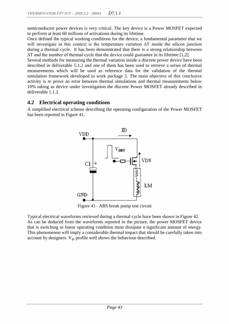
THERMINATOR FP7 ICT – 2009.3.2 - 28603 D7.1.1
Page 43
semiconductor power devices is very critical. The key device is a Power MOSFET expected
to perform at least 60 millions of activations during its lifetime.
Once defined the typical working conditions for the device, a fundamental parameter that we
will investigate in this context is the temperature variation ∆T inside the silicon junction
during a thermal cycle. It has been demonstrated that there is a strong relationship between
∆T and the number of thermal cycle that the device could guarantee in its lifetime [1,2].
Several methods for measuring the thermal variation inside a discrete power device have been
described in deliverable 5.1.2 and one of them has been used to retrieve a series of thermal
measurements which will be used as reference data for the validation of the thermal
simulation framework developed in work package 5. The main objective of this conclusive
activity is to prove an error between thermal simulations and thermal measurements below
10% taking as device under investigation the discrete Power MOSFET already described in
deliverable 1.1.2.
4.2 Electrical operating conditions
A simplified electrical scheme describing the operating configuration of the Power MOSFET
has been reported in Figure 41.
Figure 41– ABS break pump test circuit
Typical electrical waveforms retrieved during a thermal cycle have been shown in Figure 42.
As can be deduced from the waveforms reported in the picture, the power MOSFET device
that is switching in linear operating condition must dissipate a significant amount of energy.
This phenomenon will imply a considerable thermal impact that should be carefully taken into
account by designers. Vgs profile well shows the behaviour described.
THERMINATOR FP7 ICT – 2009.3.2 - 28603 D7.1.1
Page 44
Figure 42 – Voltages and currents measurements during an inductive discharge. Vgs (5V/div),
Vds (5V/div), and Ids (20A/div), time (400 us/div) during a cycle (down).
4.3 Layout modelling and mapping
The measurement equipment used for retrieving temperature information has already
described in deliverable 5.1.2 and is able to acquire thermal maps with a time resolution of
5us, more than enough for the test case under investigation.
An acquisition of the temperature in a cycle under operating conditions described in the
previous chapter has been reported in Figure 43 where a current peak of about 82A and a ∆T
peak of 53 oC have been recorded.
Starting from the layout data of the device under test described in D1.1.2, by providing the
CAD layout to the Matrix Extractor Module (Figure 44) we produced a numerical matrix
representing the physical layout composed by three bond wires stitched on the top source
metal layer. The matrix, which content has been reported in the Figure 45, is composed by a
series of indexes each one related to a physical part of the device (see WP5).

THERMINATOR FP7 ICT – 2009.3.2 - 28603 D7.1.1
Page 45
Figure 43- Drain current (up), temperature peak in P1 (down) and thermal map (right) during
a thermal cycle.
Figure 44 - Thermal-aware simulation framework flow
THERMINATOR FP7 ICT – 2009.3.2 - 28603 D7.1.1
Page 46
0000000000000000000000000000000000000000000000000000000000000 0000000888888888888888888888888888888888888888888888800000000 0000004222222222222222222222222222222222222222222222240000000 0000422222222222222222222222222222222222222222222222222240000 0004222222222222222222222222222222222222222222222222222224000 0042222222222222222222222222222222222222222222222222222224000 0042222222222222222222222222222222222222222222222222222222400 0422222222222222222222222222222222222222222222222222222222400 0422222222222222222222222222222222222222222222222222222222400 0422222222222222222222222222222222222222222222222222222222400 0422222222222222222222222222222222222222222222222222222222400 0422222222222222222222222222222222222222222222222222222222400 0422222222222222222222222222222222222222299222222222222222400 0422222222222222222222222222222222222229992222222222222222400 0422222222222222222222222222222222222999992222222222222222400 0422222222222222222222222222222222229999222222222222222222400 0422222222222222222222222222222222999992222222222222222222400 0422222222222222222222222222222229999922222222222222222222400 0422222222222222222222222222222999992222222222222222222222400 0422222222222222222222222222299999222222222222222222222222400 0422222222222222222222222229999222222222222222222222222222400 0422222222222222222222222999992222222222222222222222222222400 0422222222222222222222999992222222222222222222222222222222400 0422222222222222222299999222222222222222222222222222222222400 0422222222222222229999922222222222222222222222222222222222400 0422222222222222999992222222222222222222222222222222222222400 0422222222222299992222222222222222222222222222222222222222400 0422222222222299222222222222222222222222222222222222222222400 0422222222222222222222222222222222222222222222222222222222400 0422222222222222222222222222222222222222222222222222222222400 0422222222222222222222222222222222222222222222222222222222400 0422222222222222222222222222222222222222222222222222222222400 0422222222222222222222222222222222222222299222222222222222400 0422222222222222222222222222222222222229992222222222222222400 0422222222222222222222222222222222222999992222222222222222400 0422222222222222222222222222222222229999222222222222222222400 0422222222222222222222222222222222999992222222222222222222400 0422222222222222222222222222222229999922222222222222222222400 0422222222222222222222222222222999992222222222222222222222400 0422222222222222222222222222299999222222222222222222222222400 0422222222222222222222222229999222222222222222222222222222400 0422222222222222222222222999992222222222222222222222222222400 0422222222222222222222999992222222222222222222222222222222400 0422222222222222222299999222222222222222222222222222222222400 0422222222222222229999922222222222222222222222222222222222400 0422222222222222999992222222222222222222222222222222222222400 0422222222222299992222222222222222222222222222222222222222400 0422222222222299222222222222222222222222222222222222222222400 0422222222222222222222222222222222222222222222222222222222400 0422222222222222222222222222222222222222222222222222222222400 0422222222222222222222222222222222222222222222222222222222400 0422222222222222222222222222222222222222222222222222222222400 0422222222222222222222222222222222222222222222222222222222400 0422222222222222222222222222222222222222222222222222222222400 0422222222222222222222222222222222222222222222222222222222400 0422222222222222222222222222222222222222299222222222222222400 0422222222222222222222222222222222222229992222222222222222400 0422222222222222222222222222222222222999992222222222222222400 0422222222222222222222222222222222229999222222222222222222400 0422222222222222222222222222222222999992222222222222222222400 0422222222222222222222222222222229999922222222222222222222400 0422222222222222222222222222222999992222222222222222222222400 0422222222222222222222222222299999222222222222222222222222400 0422222222222222222222222229999222222222222222222222222222400 0422222222222222222222222999992222222222222222222222222222400 0422222222222222222222999992222222222222222222222222222222400 0422222222222222222299999222222222222222222222222222222222400 0422222222222222229999922222222222222222222222222222222222400 0422222222222222999992222222222222222222222222222222222222400 0422222222222299992222222222222222222222222222222222222222400 0422222222222299222222222222222222222222222222222222222222400 0422222222222222222222222222222222222222222222222222222222400 0422222222222222222222222222222222222222222222222222222222400 0422222222222222222222222222222222222222222222222222222222400

THERMINATOR FP7 ICT – 2009.3.2 - 28603 D7.1.1
Page 47
0422222222222222222222222222222222222222222222222222222222400 0422222222222222222222222222222222222222222222222222222222400 0422222222222222222222222222222222222222222222222222222222400 0422222222222222222222211111111111111222222222222222222222400 0422222222222222222222211111111111111222222222222222222222400 0042222222222222222222211111111111111222222222222222222222400 0042222222222222222222211111111111111222222222222222222224000 0004222222222222222222211111111111111222222222222222222224000 0000422222222222222222211111111111111222222222222222222240000 0000004222222222222222211111111111111222222222222222224000000 0000000888888888888888833333333333333888888888888888880000000 0000000000000000000000000000000000000000000000000000000000000
Figure 45 – 4453 elements matrix for the DUT
It is important to highlight that a criterion that has been used for obtaining a compromise
between complexity and accuracy (Affordability Criterion) on the final simulation is directly
related to the number of elementary cells used to generate the matrix. Figure 46 shows the
relative error on the turn-off time as a function of the number of cells in the matrix. A valid
criterion has been defined as the percentage of whole active area represented by the
elementary cell that should be at least 0.03% (Rerr<5%).
Figure 46 - Relative error on the turn-off time as a function of the number of cells in the
matrix.
In our DUT the number of elementary cells is equal to 4453 so each cell represents an amount
of area of 0.022% quite below the 0.03%. This setting should guarantee an error below the
10% as agreed in the list of Measurable Objectives (MO7.1.4).
4.4 Thermal simulations
Once the layout matrix has been generated, an elementary cell has been associated to the
active area of the device and a series of technological parameters has been extracted from the
CAD layout according to what described in D5.1.1, D5.1.2 and D5.1.3. The framework
allows to account for a distributed thermal network and hence for a non-uniform temperature
in the device. In order to extract the parameters of the thermal network, as shown in D5.1.2, a
single cell is simulated by assuming identical cells as boundary conditions. This means that
we are considering both longitudinal and transversal heat flux paths. Moreover, due to the
symmetry of the simulation (adjacent cells have the same bias configuration of the analyzed
cell), we are also considering the mutual heating of adjacent cells. Therefore we can assume
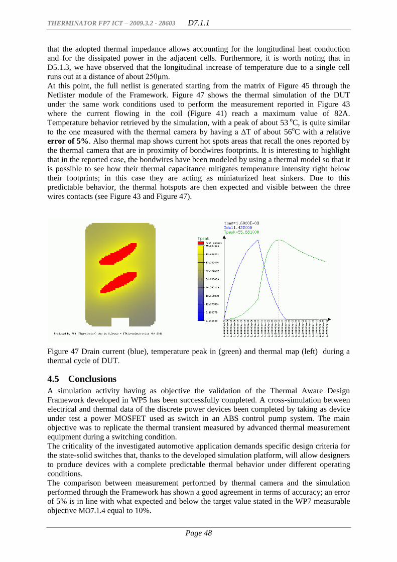
THERMINATOR FP7 ICT – 2009.3.2 - 28603 D7.1.1
Page 48
that the adopted thermal impedance allows accounting for the longitudinal heat conduction
and for the dissipated power in the adjacent cells. Furthermore, it is worth noting that in
D5.1.3, we have observed that the longitudinal increase of temperature due to a single cell
runs out at a distance of about 250μm.
At this point, the full netlist is generated starting from the matrix of Figure 45 through the
Netlister module of the Framework. Figure 47 shows the thermal simulation of the DUT
under the same work conditions used to perform the measurement reported in Figure 43
where the current flowing in the coil (Figure 41) reach a maximum value of 82A.
Temperature behavior retrieved by the simulation, with a peak of about 53 o
C, is quite similar
to the one measured with the thermal camera by having a ∆T of about 56oC with a relative
error of 5%. Also thermal map shows current hot spots areas that recall the ones reported by
the thermal camera that are in proximity of bondwires footprints. It is interesting to highlight
that in the reported case, the bondwires have been modeled by using a thermal model so that it
is possible to see how their thermal capacitance mitigates temperature intensity right below
their footprints; in this case they are acting as miniaturized heat sinkers. Due to this
predictable behavior, the thermal hotspots are then expected and visible between the three
wires contacts (see Figure 43 and Figure 47).
Figure 47 Drain current (blue), temperature peak in (green) and thermal map (left) during a
thermal cycle of DUT.
4.5 Conclusions
A simulation activity having as objective the validation of the Thermal Aware Design
Framework developed in WP5 has been successfully completed. A cross-simulation between
electrical and thermal data of the discrete power devices been completed by taking as device
under test a power MOSFET used as switch in an ABS control pump system. The main
objective was to replicate the thermal transient measured by advanced thermal measurement
equipment during a switching condition.
The criticality of the investigated automotive application demands specific design criteria for
the state-solid switches that, thanks to the developed simulation platform, will allow designers
to produce devices with a complete predictable thermal behavior under different operating
conditions.
The comparison between measurement performed by thermal camera and the simulation
performed through the Framework has shown a good agreement in terms of accuracy; an error
of 5% is in line with what expected and below the target value stated in the WP7 measurable
objective MO7.1.4 equal to 10%.

THERMINATOR FP7 ICT – 2009.3.2 - 28603 D7.1.1
Page 49
5 Contactless identification ICs (NXP-D, together with FHG)
5.1 Introduction
NXP-D has done the validation by designing and evaluation of a test chip in silicon. The
design comprises several structures to force and measure thermal effects, see Figure 48.
The silicon measurements were done on basis of the specification described in deliverable
D4.1.3. It is the first time that the CMOS 40nm process with respect to the thermal behaviour
is verified. The deliverable D4.2.1 gives an overview about the specified parameters with
respect to thermal influence on self heating of analogue circuitries. This is measured and is
evaluated on silicon.
Figure 48: Testchip Layout
FHG-EAS developed the behavioural thermal models. The work was focussed mainly on a
detailed thermal simulation of NXPs test chip. It included improvement of the FHG
simulation tool Helios towards very early analysis, identification and avoidance of critical
thermal behaviour such as hotspots or unfavourable alignment of isotherms. As an example
see Figure 49.
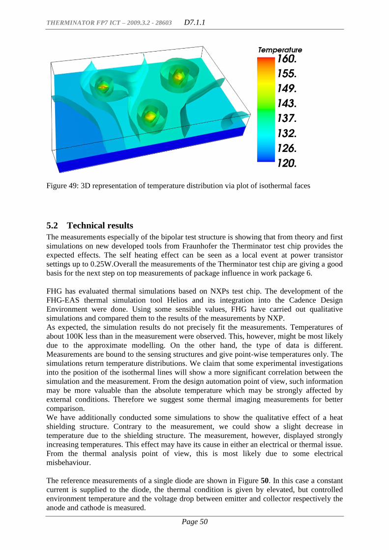
THERMINATOR FP7 ICT – 2009.3.2 - 28603 D7.1.1
Page 50
Figure 49: 3D representation of temperature distribution via plot of isothermal faces
5.2 Technical results
The measurements especially of the bipolar test structure is showing that from theory and first
simulations on new developed tools from Fraunhofer the Therminator test chip provides the
expected effects. The self heating effect can be seen as a local event at power transistor
settings up to 0.25W.Overall the measurements of the Therminator test chip are giving a good
basis for the next step on top measurements of package influence in work package 6.
FHG has evaluated thermal simulations based on NXPs test chip. The development of the
FHG-EAS thermal simulation tool Helios and its integration into the Cadence Design
Environment were done. Using some sensible values, FHG have carried out qualitative
simulations and compared them to the results of the measurements by NXP.
As expected, the simulation results do not precisely fit the measurements. Temperatures of
about 100K less than in the measurement were observed. This, however, might be most likely
due to the approximate modelling. On the other hand, the type of data is different.
Measurements are bound to the sensing structures and give point-wise temperatures only. The
simulations return temperature distributions. We claim that some experimental investigations
into the position of the isothermal lines will show a more significant correlation between the
simulation and the measurement. From the design automation point of view, such information
may be more valuable than the absolute temperature which may be strongly affected by
external conditions. Therefore we suggest some thermal imaging measurements for better
comparison.
We have additionally conducted some simulations to show the qualitative effect of a heat
shielding structure. Contrary to the measurement, we could show a slight decrease in
temperature due to the shielding structure. The measurement, however, displayed strongly
increasing temperatures. This effect may have its cause in either an electrical or thermal issue.
From the thermal analysis point of view, this is most likely due to some electrical
misbehaviour.
The reference measurements of a single diode are shown in Figure 50. In this case a constant
current is supplied to the diode, the thermal condition is given by elevated, but controlled
environment temperature and the voltage drop between emitter and collector respectively the
anode and cathode is measured.
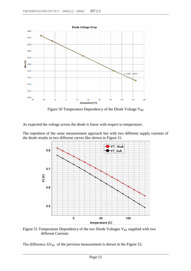
THERMINATOR FP7 ICT – 2009.3.2 - 28603 D7.1.1
Page 51
Figure 50 Temperature Dependency of the Diode Voltage VBE
As expected the voltage across the diode is linear with respect to temperature.
The repetition of the same measurement approach but with two different supply currents of
the diode results in two different curves like shown in Figure 51.
Figure 51 Temperature Dependency of the two Diode Voltages VBE supplied with two
different Currents
The difference ΔVBE of the previous measurement is shown in the Figure 52.

THERMINATOR FP7 ICT – 2009.3.2 - 28603 D7.1.1
Page 52
Figure 52 Measurement Result of ΔVBE over Temperature
As a result the ΔVBE behaviour is verified to show a linearity according to the formula
T = 6620.4*x – 276.7 [oC]
The small offset of 3K (276K instead of the expected 273K) is related to a voltage shift of the
ground level of the diodes. This effect can be seen if one puts both curves – simulated and
measured in one diagram:
Figure 53 Measured bipolar Trend Curve in Comparison to theoretical calculated Curve
The measured values (red curve) differ from the theoretical calculation (blue curve) by a
constant offset. The calculated temperature gradient of the diode is 6,62K/mV.

THERMINATOR FP7 ICT – 2009.3.2 - 28603 D7.1.1
Page 53
This curve is completely independent of any process influence. The measurements of several
different diode pairs on different devices are showing the same behaviour with the same
equation.
5.3 Conclusions
The match of measurement and modelling could be verified by evaluating a range of test
structures in the NXP test chip in comparison with the simulation results from the tool
developed by Fraunhofer. Major deviations measurement versus modelling could be
explained by the measurement- and circuit setup.
THERMINATOR FP7 ICT – 2009.3.2 - 28603 D7.1.1
Page 54
6 PSP-based advanced CMOS modelling (IMC)
6.1 Introduction
This deliverable D7.1.1 from work package 7 (WP7) describes the validation and
standardization of thermal models with main focus on validation which means the model-
hardware-correlation (MHC) itself. As described earlier in deliverable D1.3.1 the project is
based on very different practical test cases [3], which span from Power-MOSFET to analog
and digital circuits. The model-hardware-correlation described in this deliverable belongs to
test case 3 which is the datapath macrocell (digital circuit).
6.1.1 Testcase 3: Datapath Macrocell (digital circuit)
Power consumption is a key system parameter and can vary by several orders of magnitude:
From approx. 100W for high-end desktop systems down to 10W for next generation of
mobile ultrabooks and further down to smartphones with approx. 1 W in high performance
mode and <100µW in standby mode. Future digital baseband processors and application
processors represent major components for mobile applications and should deliver current
desktop computing performance at current smartphone power consumption. This means that
system design in terms of power and performance optimization for such applications is highly
challenging since high performance modes with high data rates as well as standby modes with
very limited circuit activity have to be optimized simultaneously.
Due to the different use-cases and operation modes we see a strong demand for accurate
models over a wide temperature range.
Test-case 3 is divided in 4 abstract design levels as follows:
Level Analysis Device under test (DUT)
4 static Single MOSFETs
3 dynamic Unified Logic Gates
2 dynamic Ring Oscillator
1 dynamic Critical Paths
This describes a set of digital CMOS test constructs reflecting the behaviour of digital IP
blocks. Derived from critical path information, the different sub-cases provide information
about digital circuit behaviour on different abstraction levels.
This deliverable will cover mainly levels 4 to 2, initial results have been partially reported in
WP1 and WP2 already (e.g. deliverable D1.1.1 [4] and D2.1.2 [5]). Furthermore test case
level 1 will be described in more detail in deliverable D7.2.1 “Demonstration of thermal-
aware design techniques” [6].
6.1.2 40nm versus 28nm technology
Besides the link to the actual test-case we also briefly summarize the technological
differences of the 40nm and 28nm technologies on a generic level. Due to the diversity of
partners and applications and the modular nature of process flows we face many possible
technology flavours. Therefore we reference towards the international semiconductor
roadmap (ITRS) if applicable.
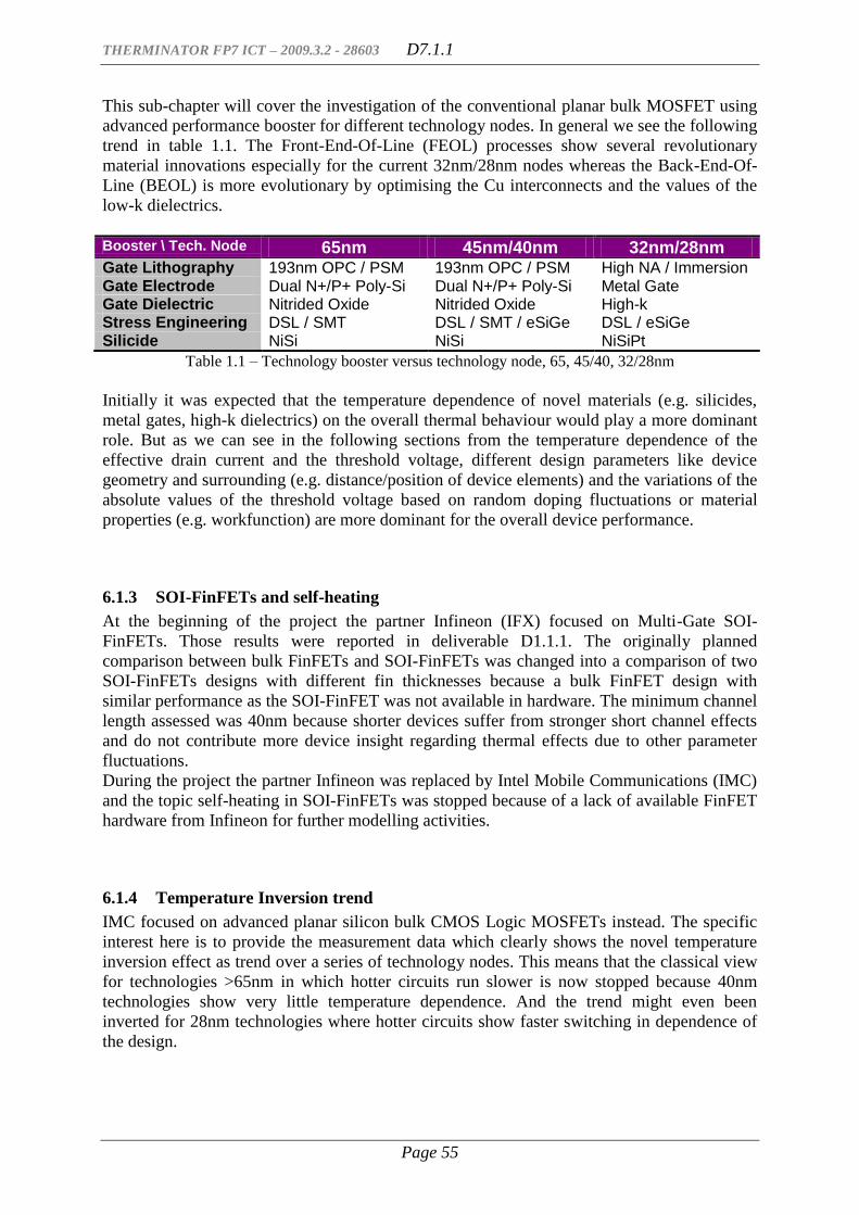
THERMINATOR FP7 ICT – 2009.3.2 - 28603 D7.1.1
Page 55
This sub-chapter will cover the investigation of the conventional planar bulk MOSFET using
advanced performance booster for different technology nodes. In general we see the following
trend in table 1.1. The Front-End-Of-Line (FEOL) processes show several revolutionary
material innovations especially for the current 32nm/28nm nodes whereas the Back-End-Of-
Line (BEOL) is more evolutionary by optimising the Cu interconnects and the values of the
low-k dielectrics.
Booster \ Tech. Node 65nm 45nm/40nm 32nm/28nm Gate Lithography 193nm OPC / PSM 193nm OPC / PSM High NA / Immersion Gate Electrode Dual N+/P+ Poly-Si Dual N+/P+ Poly-Si Metal Gate Gate Dielectric Nitrided Oxide Nitrided Oxide High-k Stress Engineering DSL / SMT DSL / SMT / eSiGe DSL / eSiGe Silicide NiSi NiSi NiSiPt
Table 1.1 – Technology booster versus technology node, 65, 45/40, 32/28nm
Initially it was expected that the temperature dependence of novel materials (e.g. silicides,
metal gates, high-k dielectrics) on the overall thermal behaviour would play a more dominant
role. But as we can see in the following sections from the temperature dependence of the
effective drain current and the threshold voltage, different design parameters like device
geometry and surrounding (e.g. distance/position of device elements) and the variations of the
absolute values of the threshold voltage based on random doping fluctuations or material
properties (e.g. workfunction) are more dominant for the overall device performance.
6.1.3 SOI-FinFETs and self-heating
At the beginning of the project the partner Infineon (IFX) focused on Multi-Gate SOI-
FinFETs. Those results were reported in deliverable D1.1.1. The originally planned
comparison between bulk FinFETs and SOI-FinFETs was changed into a comparison of two
SOI-FinFETs designs with different fin thicknesses because a bulk FinFET design with
similar performance as the SOI-FinFET was not available in hardware. The minimum channel
length assessed was 40nm because shorter devices suffer from stronger short channel effects
and do not contribute more device insight regarding thermal effects due to other parameter
fluctuations.
During the project the partner Infineon was replaced by Intel Mobile Communications (IMC)
and the topic self-heating in SOI-FinFETs was stopped because of a lack of available FinFET
hardware from Infineon for further modelling activities.
6.1.4 Temperature Inversion trend
IMC focused on advanced planar silicon bulk CMOS Logic MOSFETs instead. The specific
interest here is to provide the measurement data which clearly shows the novel temperature
inversion effect as trend over a series of technology nodes. This means that the classical view
for technologies >65nm in which hotter circuits run slower is now stopped because 40nm
technologies show very little temperature dependence. And the trend might even been
inverted for 28nm technologies where hotter circuits show faster switching in dependence of
the design.
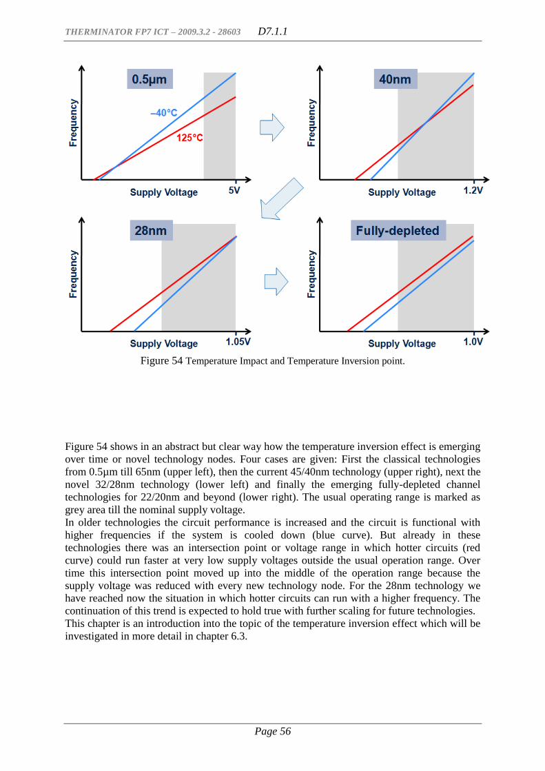
THERMINATOR FP7 ICT – 2009.3.2 - 28603 D7.1.1
Page 56
Figure 54 Temperature Impact and Temperature Inversion point.
Figure 54 shows in an abstract but clear way how the temperature inversion effect is emerging
over time or novel technology nodes. Four cases are given: First the classical technologies
from 0.5µm till 65nm (upper left), then the current 45/40nm technology (upper right), next the
novel 32/28nm technology (lower left) and finally the emerging fully-depleted channel
technologies for 22/20nm and beyond (lower right). The usual operating range is marked as
grey area till the nominal supply voltage.
In older technologies the circuit performance is increased and the circuit is functional with
higher frequencies if the system is cooled down (blue curve). But already in these
technologies there was an intersection point or voltage range in which hotter circuits (red
curve) could run faster at very low supply voltages outside the usual operation range. Over
time this intersection point moved up into the middle of the operation range because the
supply voltage was reduced with every new technology node. For the 28nm technology we
have reached now the situation in which hotter circuits can run with a higher frequency. The
continuation of this trend is expected to hold true with further scaling for future technologies.
This chapter is an introduction into the topic of the temperature inversion effect which will be
investigated in more detail in chapter 6.3.

THERMINATOR FP7 ICT – 2009.3.2 - 28603 D7.1.1
Page 57
6.1.5 Therminator project objectives
Therminator project objective #1: New modeling and simulation capabilities to support
accurate circuit thermal analysis and simulation
WP7 measurable objective #1:
Error between measurements and simulation within 20% [IMC] (MO7.1.6 see e.g. fig. 2.3 and
3.12, chapter 2 & 3)
Therminator project objective #2. Innovative thermal-aware design techniques, methodologies
and prototype tools for controlling, compensating and managing thermally-induced effects on
parameters such as timing, (dynamic and leakage) power, reliability and yield
WP7 measurable objective #2:
Determine the temperature inversion intersection point of two temperatures corresponding supply
voltage within 20% for relevant parameters as performance and Ion (MO7.1.7 see chapter 2 &
3).
Therminator project objective #3. Demonstration of the accuracy and ease of integration within
existing design flows of the new models by validation against measured data obtained on ad-hoc
silicon structures
WP7 measurable objective #3:
Validate the high-k metal gate 28nm CMOS models developed in WP2, with cross-technology
reference to 40 nm. Error between measurements and simulation within 20% [IMC] (MO7.1.8
see e.g. fig. 3.12, chapter 3)
Therminator project objective #4. Demonstration of the applicability and effectiveness of the
new design solutions through manufacturing of test-chips featuring leading-edge silicon
technology, as available from some of the project partners
WP7 measurable objective #4:
Demonstration of model hardware correlation based on 40nm and 28nm testchips, i.e. one or more
testchips per technology. (MO7.1.9 testchips as vehicles to achieve results demonstrated)
Therminator project objective #5. Demonstration of the usability and effectiveness of the new
design methodologies and tools by their application to industry-strength design cases made
available by some of the project partners WP7 measurable objective #5:
The circuit-referenced PSP-methodology is 100% compatible to the IMC design flow.
(MO7.1.10 see conclusion section 6.4)
6.2 40nm Model-Hardware-Correlation (MHC) results
6.2.1 Device level model to hardware correlation including devices for analog usage
The DC model to silicon correlation is shown in Figure 55 as a function of physical gate-
length for p-FETs of regular VT device flavour (RVT). Lines show the simulation values of
the IMC- 40nm model, which is a BSIM 4.5 model, symbols are the measured values of a
device chosen by multi-golden device selection with the temperature as parameter, compared
here for the range from -40°C to 110°C with intermediate steps at 25°C and at 85°C. Figure
56 shows the corresponding plots for n-RVT devices. The x-axis in all of the 4 sub-plots
covers a wide range of device gate length starting with a subnominal device of ~35nm to a
maximum device length of 9µm. All design relevant gate lengths are covered by dedicated
test structures, the nominal gate length of 40nm is used for digital and library cells, a 50nm
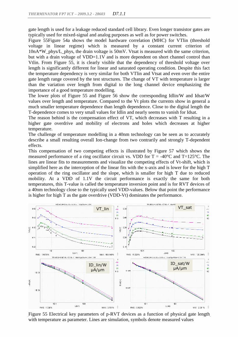
THERMINATOR FP7 ICT – 2009.3.2 - 28603 D7.1.1
Page 58
gate length is used for a leakage reduced standard cell library. Even longer transistor gates are
typically used for mixed-signal and analog purposes as well as for power switches.
Figure 55Figure 54a shows the model hardware correlation (MHC) for VTlin (threshold
voltage in linear regime) which is measured by a constant current criterion of
10nA*W_phys/L_phys, the drain voltage is 50mV. Vtsat is measured with the same criterion,
but with a drain voltage of VDD=1.1V and is more dependent on short channel control than
Vtlin. From Figure 55, it is clearly visible that the dependency of threshold voltage over
length is significantly different for linear and saturated operating condition. Despite this fact
the temperature dependency is very similar for both VTlin and Vtsat and even over the entire
gate length range covered by the test structures. The change of VT with temperature is larger
than the variation over length from digital to the long channel device emphasizing the
importance of a good temperature modelling.
The lower plots of Figure 55 and Figure 56 show the corresponding Idlin/W and Idsat/W
values over length and temperature. Compared to the Vt plots the currents show in general a
much smaller temperature dependence than length dependence. Close to the digital length the
T-dependence comes to very small values for Idlin and nearly seems to vanish for Idsat.
The reason behind is the compensation effect of VT, which decreases with T resulting in a
higher gate overdrive and mobility of electrons and holes which decreases at higher
temperature.
The challenge of temperature modelling in a 40nm technology can be seen as to accurately
describe a small resulting overall Ion-change from two contrarily and strongly T-dependent
effects.
This compensation of two competing effects is illustrated by Figure 57 which shows the
measured performance of a ring oscillator circuit vs. VDD for T = -40°C and T=125°C. The
lines are linear fits to measurements and visualize the competing effects of Vt-shift, which is
simplified here as the interception of the linear fits with the x-axis and is lower for the high T
operation of the ring oscillator and the slope, which is smaller for high T due to reduced
mobility. At a VDD of 1.1V the circuit performance is exactly the same for both
temperatures, this T-value is called the temperature inversion point and is for RVT devices of
a 40nm technology close to the typically used VDD-values. Below that point the performance
is higher for high T as the gate overdrive (VDD-Vt) dominates the performance.
VT_lin VT_sat
ID_lin/W
µA/µm
ID_sat/W
µA/µm
Figure 55 Electrical key parameters of p-RVT devices as a function of physical gate length
with temperature as parameter. Lines are simulation, symbols denote measured values
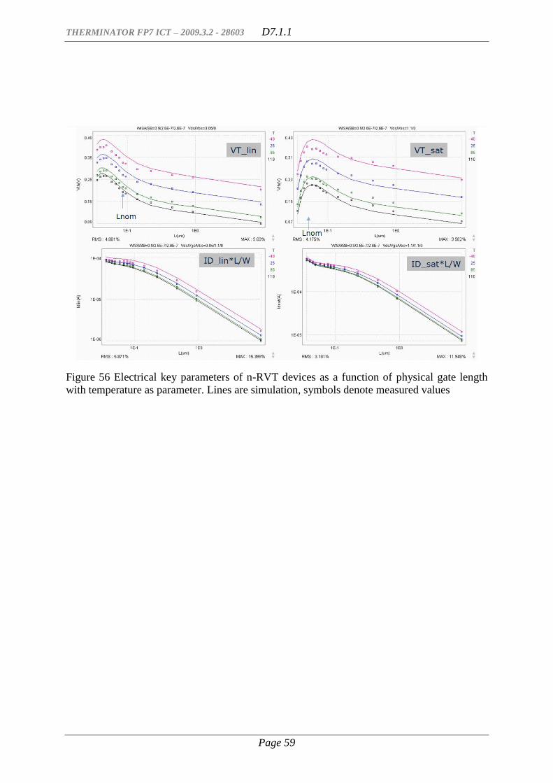
THERMINATOR FP7 ICT – 2009.3.2 - 28603 D7.1.1
Page 59
Figure 56 Electrical key parameters of n-RVT devices as a function of physical gate length
with temperature as parameter. Lines are simulation, symbols denote measured values

THERMINATOR FP7 ICT – 2009.3.2 - 28603 D7.1.1
Page 60
Figure 57 Measured circuit performance (ring oscillator) vs. VDD for T = -40°C (dark blue
symbols) and T=125°C (purple symbols). The lines are linear fits to measurements and
illustrate the competing effects of Vt-shift (interception of fits with x-axis, lower for high T)
and slope, smaller for high T
Above the temperature inversion point the higher mobility of the low T operation has the
bigger impact.
While Figure 55 and Figure 56 show that the modelling quality for all of the DC key
parameter is decent over the whole length range, Figure 58 – Figure 60 allow a closer look on
the consistency of model and measurement data. These plots show the VTsat and Ion vs. T-
behavior for 3 design relevant gate lengths representing digital, mixed signal and analog
devices. Thereby, the model is the same as used for Figure 55 and Figure 56, but hardware is
from a different 40nm technology source which was aligned with respect to fulfil IMC´s
product requirements.
For the digital length in Figure 58 the VT decrease over the measured T-range from -40°C to
110°C is about 160mV for both, n- and p-RVT, the Ion decrease with T is only 4% for p-RVT
and about 10% for n-RVT. Figure 59 represents an intermediate gate length typically used for
analog circuits, here the VT change with T is quite similar to the digital length but Ion is
much more reduced with about 14% for both, n- and p-RVT. For long channel devices
(Figure 60) the VT decrease is still very similar to the digital and analog length, but Ion is
reduced drastically over T with ~20% for p-RVT and as much as 40% for the n-RVT long
channel device. Despite this qualitative change of Ion vs. T for the different devices the IMC
model as developed for silicon of source 1 is capable of well describing also the Si of a 2nd
source.
0.0E+00
5.0E+04
1.0E+05
1.5E+05
2.0E+05
2.5E+05
3.0E+05
3.5E+05
0 0.5 1 1.5
Rin
gO
Fre
qu
ency
[H
z]
VDD [V]
T=-40°C
T=125°C

THERMINATOR FP7 ICT – 2009.3.2 - 28603 D7.1.1
Page 61
Figure 58 - Electrical key parameters of p-RVT (left side) and n-RVT (right side) for T-
dependent change of VTsat and Ion for RVT devices of nominal length, normalized to room
temperature. Targets (shown in purple) are model values, measurement values are shown in
blue

THERMINATOR FP7 ICT – 2009.3.2 - 28603 D7.1.1
Page 62
Figure 59 Electrical key parameters of p-RVT (left side) and n-RVT (right side) for T-
dependent change of VTsat and Ion for RVT devices of intermediate length as typically used
for analog circuits, normalized to room temperature. Targets (shown in purple) are model
values, measurement values are shown in blue
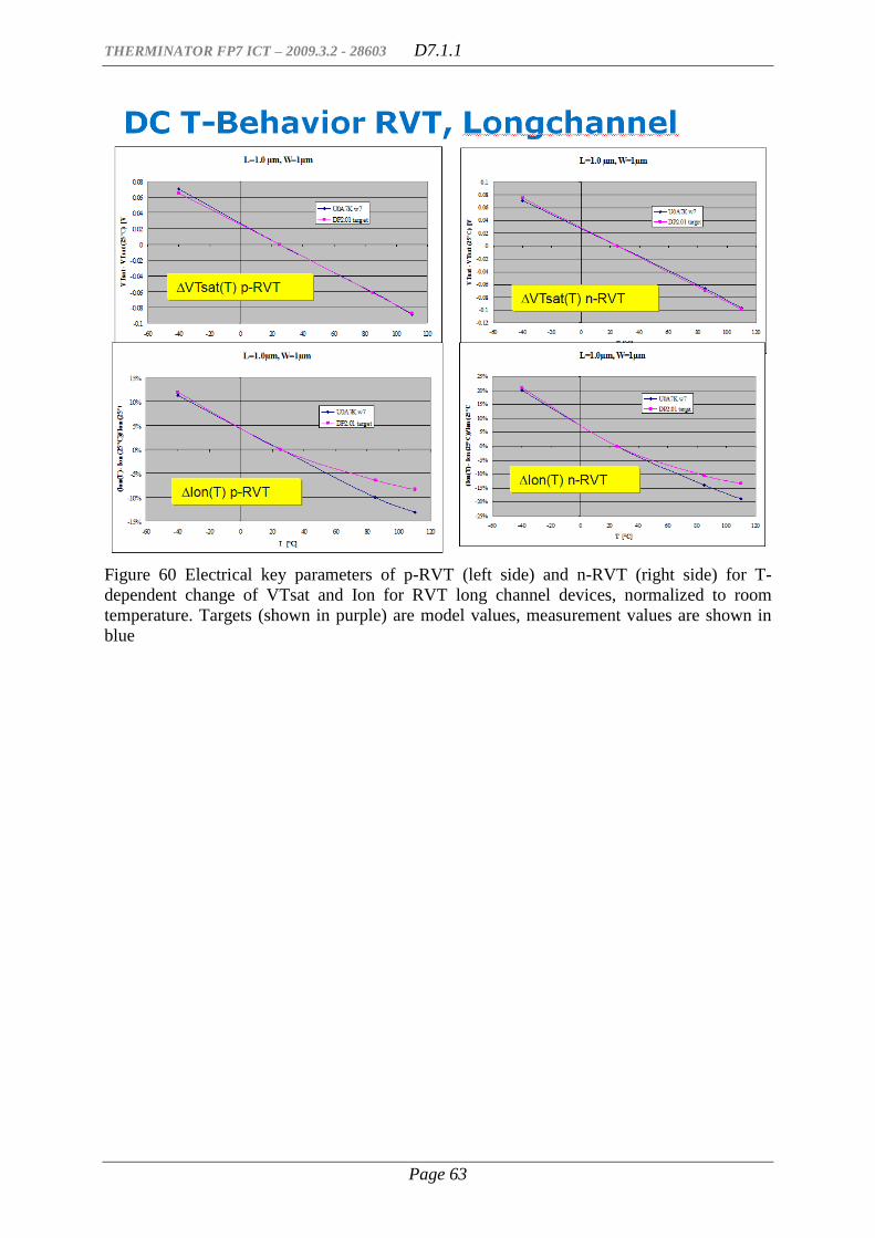
THERMINATOR FP7 ICT – 2009.3.2 - 28603 D7.1.1
Page 63
Figure 60 Electrical key parameters of p-RVT (left side) and n-RVT (right side) for T-
dependent change of VTsat and Ion for RVT long channel devices, normalized to room
temperature. Targets (shown in purple) are model values, measurement values are shown in
blue
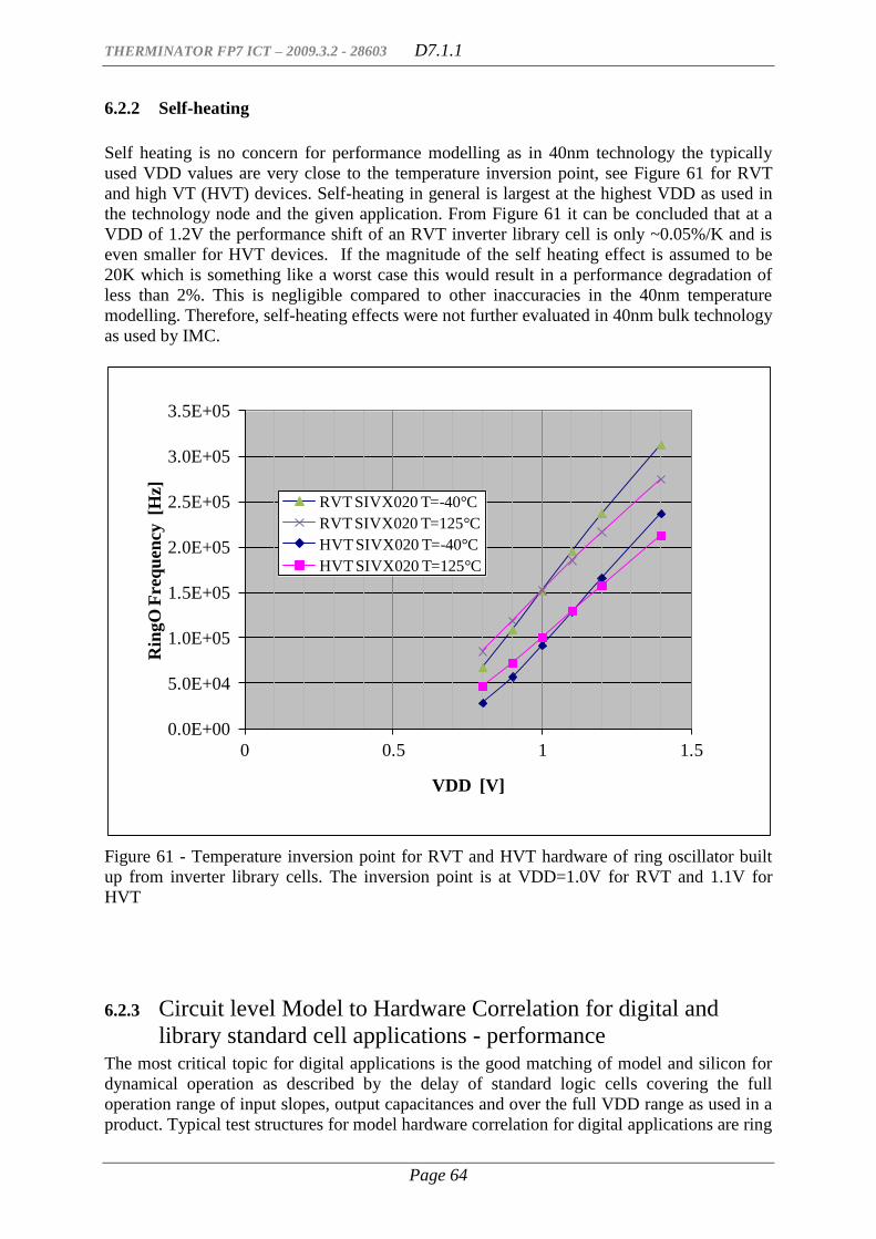
THERMINATOR FP7 ICT – 2009.3.2 - 28603 D7.1.1
Page 64
6.2.2 Self-heating
Self heating is no concern for performance modelling as in 40nm technology the typically
used VDD values are very close to the temperature inversion point, see Figure 61 for RVT
and high VT (HVT) devices. Self-heating in general is largest at the highest VDD as used in
the technology node and the given application. From Figure 61 it can be concluded that at a
VDD of 1.2V the performance shift of an RVT inverter library cell is only ~0.05%/K and is
even smaller for HVT devices. If the magnitude of the self heating effect is assumed to be
20K which is something like a worst case this would result in a performance degradation of
less than 2%. This is negligible compared to other inaccuracies in the 40nm temperature
modelling. Therefore, self-heating effects were not further evaluated in 40nm bulk technology
as used by IMC.
Figure 61 - Temperature inversion point for RVT and HVT hardware of ring oscillator built
up from inverter library cells. The inversion point is at VDD=1.0V for RVT and 1.1V for
HVT
6.2.3 Circuit level Model to Hardware Correlation for digital and
library standard cell applications - performance
The most critical topic for digital applications is the good matching of model and silicon for
dynamical operation as described by the delay of standard logic cells covering the full
operation range of input slopes, output capacitances and over the full VDD range as used in a
product. Typical test structures for model hardware correlation for digital applications are ring
0.0E+00
5.0E+04
1.0E+05
1.5E+05
2.0E+05
2.5E+05
3.0E+05
3.5E+05
0 0.5 1 1.5
Rin
gO
Fre
qu
ency
[H
z]
VDD [V]
RVT SIVX020 T=-40°C
RVT SIVX020 T=125°C
HVT SIVX020 T=-40°C
HVT SIVX020 T=125°C
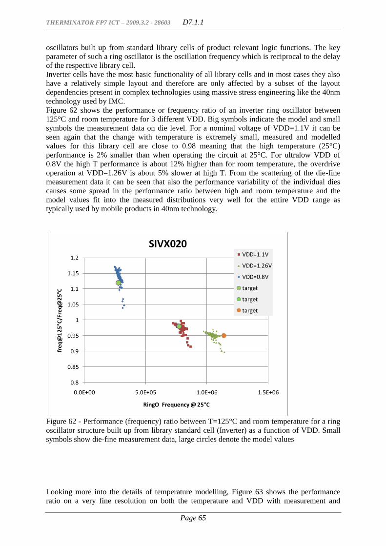
THERMINATOR FP7 ICT – 2009.3.2 - 28603 D7.1.1
Page 65
oscillators built up from standard library cells of product relevant logic functions. The key
parameter of such a ring oscillator is the oscillation frequency which is reciprocal to the delay
of the respective library cell.
Inverter cells have the most basic functionality of all library cells and in most cases they also
have a relatively simple layout and therefore are only affected by a subset of the layout
dependencies present in complex technologies using massive stress engineering like the 40nm
technology used by IMC.
Figure 62 shows the performance or frequency ratio of an inverter ring oscillator between
125°C and room temperature for 3 different VDD. Big symbols indicate the model and small
symbols the measurement data on die level. For a nominal voltage of VDD=1.1V it can be
seen again that the change with temperature is extremely small, measured and modelled
values for this library cell are close to 0.98 meaning that the high temperature (25°C)
performance is 2% smaller than when operating the circuit at 25°C. For ultralow VDD of
0.8V the high T performance is about 12% higher than for room temperature, the overdrive
operation at VDD=1.26V is about 5% slower at high T. From the scattering of the die-fine
measurement data it can be seen that also the performance variability of the individual dies
causes some spread in the performance ratio between high and room temperature and the
model values fit into the measured distributions very well for the entire VDD range as
typically used by mobile products in 40nm technology.
Figure 62 - Performance (frequency) ratio between T=125°C and room temperature for a ring
oscillator structure built up from library standard cell (Inverter) as a function of VDD. Small
symbols show die-fine measurement data, large circles denote the model values
Looking more into the details of temperature modelling, Figure 63 shows the performance
ratio on a very fine resolution on both the temperature and VDD with measurement and
0.8
0.85
0.9
0.95
1
1.05
1.1
1.15
1.2
0.0E+00 5.0E+05 1.0E+06 1.5E+06
fre
q@
12
5°C
/Fre
q@2
5°C
RingO Frequency @ 25°C
SIVX020 VDD=1.1V
VDD=1.26V
VDD=0.8V
target
target
target

THERMINATOR FP7 ICT – 2009.3.2 - 28603 D7.1.1
Page 66
model values at temperatures of -40°C, -10°C, 25°C, 55°C, 85°C, 125°C and VDD from as
low as 0.8V to a very high overdrive voltage of 1.4V in steps of only 0.1V. A 2-input NAND
has been chosen for this detailed comparison because it highly uses standard cells and it is
already a more complex library cell using transistors in series operation.
Figure 64 shows the deviations between model and measurement for all of the operating
conditions and data as shown in Figure 63. It can be easily seen that for most of the operating
conditions the model hardware correlation is in a narrow band of +/-2%. The biggest
discrepancies occur at low temperature which is mostly related to the shortcomings of the
BSIM 4.5 model. This will be improved in future technologies by using PSP as the compact
model for device modelling and circuit simulation, see chapter 6.3.
Figure 63 - Temperature and VDD dependent comparison of model and Si measurement for a
ring oscillator built up from 2-input NAND library cells (RVT). Normalized to performance
at room temperature. Lines show model values, symbols indicate measurements
-15%
-10%
-5%
0%
5%
10%
15%
-50 0 50 100 150
per
form
ance
del
ta
T [°C]
SND2X020
meas VDD=0.8V
meas VDD=0.9V
meas VDD=1.0V
meas VDD=1.1V
meas VDD=1.2V
meas VDD=1.4V
sim VDD=0.8V
sim VDD=0.9V
sim VDD=1.0V
sim VDD=1.1V
sim VDD=1.2V
sim VDD=1.4V
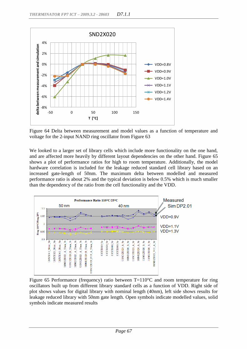
THERMINATOR FP7 ICT – 2009.3.2 - 28603 D7.1.1
Page 67
Figure 64 Delta between measurement and model values as a function of temperature and
voltage for the 2-input NAND ring oscillator from Figure 63
We looked to a larger set of library cells which include more functionality on the one hand,
and are affected more heavily by different layout dependencies on the other hand. Figure 65
shows a plot of performance ratios for high to room temperature. Additionally, the model
hardware correlation is included for the leakage reduced standard cell library based on an
increased gate-length of 50nm. The maximum delta between modelled and measured
performance ratio is about 2% and the typical deviation is below 0.5% which is much smaller
than the dependency of the ratio from the cell functionality and the VDD.
Figure 65 Performance (frequency) ratio between T=110°C and room temperature for ring
oscillators built up from different library standard cells as a function of VDD. Right side of
plot shows values for digital library with nominal length (40nm), left side shows results for
leakage reduced library with 50nm gate length. Open symbols indicate modelled values, solid
symbols indicate measured results
-8%
-6%
-4%
-2%
0%
2%
4%
-50 0 50 100 150de
lta
be
twe
en
me
asu
rem
ent
and
sim
ula
tio
n
T [°C]
SND2X020
VDD=0.8V
VDD=0.9V
VDD=1.0V
VDD=1.1V
VDD=1.2V
VDD=1.4V
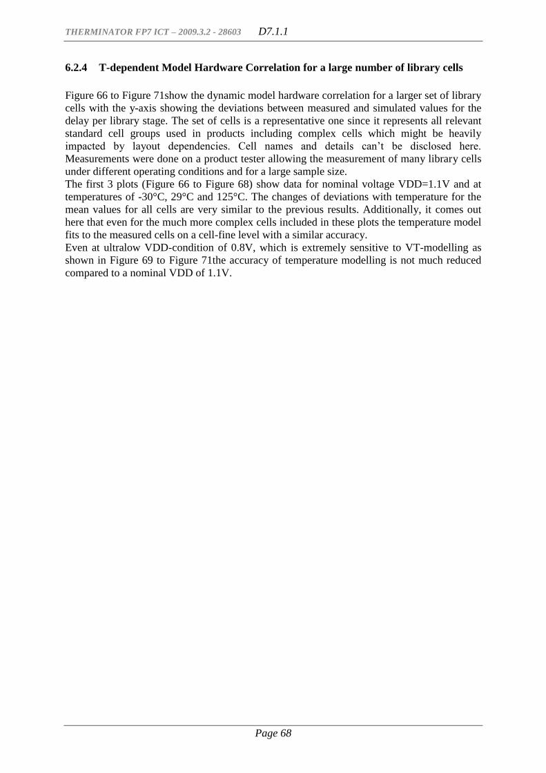
THERMINATOR FP7 ICT – 2009.3.2 - 28603 D7.1.1
Page 68
6.2.4 T-dependent Model Hardware Correlation for a large number of library cells
Figure 66 to Figure 71show the dynamic model hardware correlation for a larger set of library
cells with the y-axis showing the deviations between measured and simulated values for the
delay per library stage. The set of cells is a representative one since it represents all relevant
standard cell groups used in products including complex cells which might be heavily
impacted by layout dependencies. Cell names and details can’t be disclosed here.
Measurements were done on a product tester allowing the measurement of many library cells
under different operating conditions and for a large sample size.
The first 3 plots (Figure 66 to Figure 68) show data for nominal voltage VDD=1.1V and at
temperatures of -30°C, 29°C and 125°C. The changes of deviations with temperature for the
mean values for all cells are very similar to the previous results. Additionally, it comes out
here that even for the much more complex cells included in these plots the temperature model
fits to the measured cells on a cell-fine level with a similar accuracy.
Even at ultralow VDD-condition of 0.8V, which is extremely sensitive to VT-modelling as
shown in Figure 69 to Figure 71the accuracy of temperature modelling is not much reduced
compared to a nominal VDD of 1.1V.
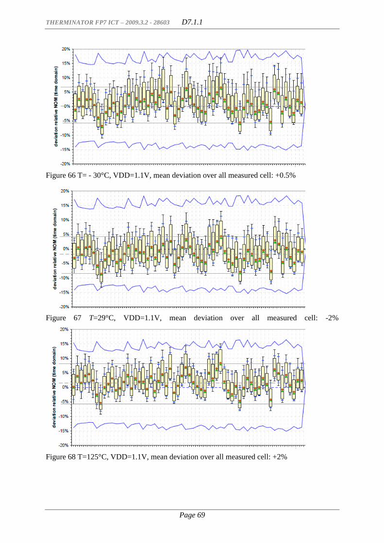
THERMINATOR FP7 ICT – 2009.3.2 - 28603 D7.1.1
Page 69
Figure 66 T= - 30°C, VDD=1.1V, mean deviation over all measured cell: +0.5%
Figure 67 T=29°C, VDD=1.1V, mean deviation over all measured cell: -2%
Figure 68 T=125°C, VDD=1.1V, mean deviation over all measured cell: +2%
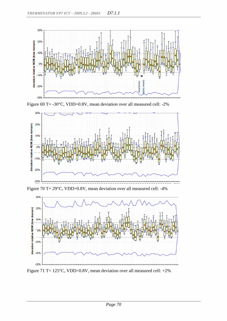
THERMINATOR FP7 ICT – 2009.3.2 - 28603 D7.1.1
Page 70
Figure 69 T= -30°C, VDD=0.8V, mean deviation over all measured cell: -2%
Figure 70 T= 29°C, VDD=0.8V, mean deviation over all measured cell: -4%
Figure 71 T= 125°C, VDD=0.8V, mean deviation over all measured cell: +2%
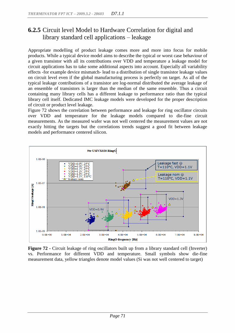
THERMINATOR FP7 ICT – 2009.3.2 - 28603 D7.1.1
Page 71
6.2.5 Circuit level Model to Hardware Correlation for digital and
library standard cell applications – leakage
Appropriate modelling of product leakage comes more and more into focus for mobile
products. While a typical device model aims to describe the typical or worst case behaviour of
a given transistor with all its contributions over VDD and temperature a leakage model for
circuit applications has to take some additional aspects into account. Especially all variability
effects -for example device mismatch- lead to a distribution of single transistor leakage values
on circuit level even if the global manufacturing process is perfectly on target. As all of the
typical leakage contributions of a transistor are log-normal distributed the average leakage of
an ensemble of transistors is larger than the median of the same ensemble. Thus a circuit
containing many library cells has a different leakage to performance ratio than the typical
library cell itself. Dedicated IMC leakage models were developed for the proper description
of circuit or product level leakage.
Figure 72 shows the correlation between performance and leakage for ring oscillator circuits
over VDD and temperature for the leakage models compared to die-fine circuit
measurements. As the measured wafer was not well centered the measurement values are not
exactly hitting the targets but the correlations trends suggest a good fit between leakage
models and performance centered silicon.
Figure 72 - Circuit leakage of ring oscillators built up from a library standard cell (Inverter)
vs. Performance for different VDD and temperature. Small symbols show die-fine
measurement data, yellow triangles denote model values (Si was not well centered to target)
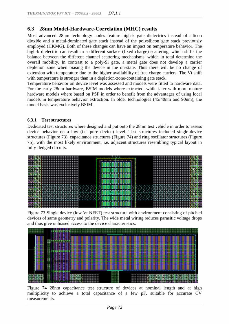
THERMINATOR FP7 ICT – 2009.3.2 - 28603 D7.1.1
Page 72
6.3 28nm Model-Hardware-Correlation (MHC) results
Most advanced 28nm technology nodes feature high-k gate dielectrics instead of silicon
dioxide and a metal-dominated gate stack instead of the polysilicon gate stack previously
employed (HKMG). Both of these changes can have an impact on temperature behavior. The
high-k dielectric can result in a different surface (fixed charge) scattering, which shifts the
balance between the different channel scattering mechanisms, which in total determine the
overall mobility. In contrast to a poly-Si gate, a metal gate does not develop a carrier
depletion zone when biasing the device in the on-state. Thus there will be no change of
extension with temperature due to the higher availability of free charge carriers. The Vt shift
with temperature is stronger than in a depletion-zone-containing gate stack.
Temperature behavior on device level was assessed and models were fitted to hardware data.
For the early 28nm hardware, BSIM models where extracted, while later with more mature
hardware models where based on PSP in order to benefit from the advantages of using local
models in temperature behavior extraction. In older technologies (45/40nm and 90nm), the
model basis was exclusively BSIM.
6.3.1 Test structures
Dedicated test structures where designed and put onto the 28nm test vehicle in order to assess
device behavior on a low (i.e. pure device) level. Test structures included single-device
structures (Figure 73), capacitance structures (Figure 74) and ring oscillator structures (Figure
75), with the most likely environment, i.e. adjacent structures resembling typical layout in
fully fledged circuits.
Figure 73 Single device (low Vt NFET) test structure with environment consisting of pitched
devices of same geometry and polarity. The wide metal wiring reduces parasitic voltage drops
and thus give unbiased access to the device characteristics.
Figure 74 28nm capacitance test structure of devices at nominal length and at high
multiplicity to achieve a total capacitance of a few pF, suitable for accurate CV
measurements.
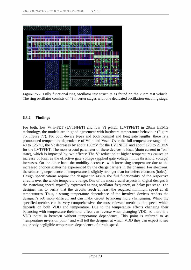
THERMINATOR FP7 ICT – 2009.3.2 - 28603 D7.1.1
Page 73
Figure 75 - Fully functional ring oscillator test structure as found on the 28nm test vehicle.
The ring oscillator consists of 49 inverter stages with one dedicated oscillation-enabling stage.
6.3.2 Findings
For both, low Vt n-FET (LVTNFET) and low Vt p-FET (LVTPFET) in 28nm HKMG
technology, the models are in good agreement with hardware temperature behaviour (Figure
76, Figure 77). For both device types and both nominal and long gate lengths, there is a
pronounced temperature dependence of Vtlin and Vtsat: Over the full temperature range of -
40 to 125 °C, the Vt decreases by about 160mV for the LVTNFET and about 170 to 210mV
for the LVTPFET. The most crucial parameter of these devices is Idsat (drain current in “on”
state), which is impacted by two effects: The Vt reduction at higher temperatures causes an
increase of Idsat as the effective gate voltage (applied gate voltage minus threshold voltage)
increases. On the other hand the mobility decreases with increasing temperature due to the
increased phonon scattering experienced by the charge carriers in the channel. For electrons,
the scattering dependence on temperature is slightly stronger than for defect electrons (holes).
Design specifications require the designer to assure the full functionality of the respective
circuits over the whole temperature range. One of the most crucial aspects in digital designs is
the switching speed, typically expressed as ring oscillator frequency, or delay per stage. The
designer has to verify that the circuits reach at least the required minimum speed at all
temperatures. Thus, a strong temperature dependence of the involved devices renders the
designer’s job more difficult and can make circuit balancing more challenging. While the
specified metrics can be very comprehensive, the most relevant metric is the speed, which
depends on both VDD and temperature. Due to the temperature effects changing their
balancing with temperature their total effect can reverse when changing VDD, so there is a
VDD point in between without temperature dependence. This point is referred to as
“temperature inversion point” and will tell the designer at which VDD they can expect to see
no or only negligible temperature dependence of circuit speed.
THERMINATOR FP7 ICT – 2009.3.2 - 28603 D7.1.1
Page 74
Figure 76 - Temperature behaviour of key device parameters for 28nm HKMG LVTNFET
device. a) Vtlin, b) Vtsat, c) Idlin, d) Idsat. Model behaviour (blue lines) is in good agreement
with measurement data (red squares). Due to the dominating effect of Vt over mobility
temperature behaviour, Idsat decreases with increasing temperature.
THERMINATOR FP7 ICT – 2009.3.2 - 28603 D7.1.1
Page 75
Figure 77 - Temperature behaviour of key device parameters for 28nm HKMG LVTPFET
device. a) Vtlin, b) Vtsat, c) Idlin, d) Idsat. Model behaviour (blue lines) is in good agreement
with measurement data (red squares). Due to the strong hole mobility temperature
dependence, which exhibits a strong increase with T, the effect of Vt drop is overcompensated
and Idsat increases with temperature for short device lengths.
The cross-technology comparison shows that at previous technologies, one would see e.g. in
90nm technology a temperature inversion point of about 0.85V (Figure 78), which is below
the nominal VDD of typically 1.0V. Both at high and low temperature, the model accurately
predicts hardware behaviour (delta less than 2%). The blue line (-30 °C) shows that for
VDD>0.85, the ring oscillator is running faster (less delay) than at room temperature. At high
temperatures the ring oscillator is running slower. The effects is more pronounced at higher
VDDs, reaching a total delta of about 10% slower at 125 °C and 5 % faster at -30 °C. For low
VDD, there is less effect as the devices are being operated closer to their respective threshold
voltages, thus rendering the Vt vs. T behaviour the dominating one. The temperature
inversion point (VDD for which there is no temperature dependence seen) for ring oscillators
with nominal gate length is found for very low VDD at around 0.85V.

THERMINATOR FP7 ICT – 2009.3.2 - 28603 D7.1.1
Page 76
Figure 78 Delay of 90nm technology ring oscillators plotted as relative delay differences with
respect to room temperature delay. Hardware data as symbols, model results as lines.
In 40nm technology, the temperature inversion point is found at about 1.0V for regular-Vt
devices and 1.1V for high-Vt devices (Figure 79) while the nominal VDD is 1.1V. This
behaviour is expected as the devices in both regular-Vt and high-Vt ring oscillators need
about the same effective gate voltage overdrive (gate voltage minus Vt) to compensate the
mobility effect.
At low VDD, the frequency increases with temperature, as the temperature behaviour of Vt
dominates the device performance over the mobility behaviour. With increasing VDD, the
mobility effect (reduction of mobility with increasing temperature) is getting stronger and
dominates at high VDD.
Thus, 40nm designs have the benefit of having a very benign temperature effect at the most
typical circuit supply voltages, which helps in building reliable designs (being functional over
the whole temperature range). In 28nm technology, one will find the temperature inversion
point at about 1.1V (fig 3.11) while the nominal VDD is 1.0V, so a standard design using
nominal VDD will see a slight increase of speed with temperature - opposite to earlier
technologies as 90nm mentioned above where a decrease of speed with temperature is
observed.
Thus, an accurate reflection of temperature behaviour has more impact on 28nm designs than
for the previous generation of 40nm designs.
THERMINATOR FP7 ICT – 2009.3.2 - 28603 D7.1.1
Page 77
Figure 79 Ring oscillator frequency vs temperature for different VDDs in 40nm technology.
High-Vt devices in blue, regular Vt devices in pink. Left column: absolute frequency vs T,
right column: relative frequency difference with respect to room temperature frequency. Top
to bottom: Increasing VDD of 0.8V, 1.0V, 1.2V and 1.4V.
Figure 80 shows in 28nm technology the ring oscillator frequency as function of temperature
for different VDDs. Measurement data are compared with BSIM models on the one hand, and
THERMINATOR FP7 ICT – 2009.3.2 - 28603 D7.1.1
Page 78
with PSP models on the other hand. The PSP models, which have been extracted with taking
advantage of PSP’s local model support, give a better fit to hardware than the BSIM models
in the most relevant temperature range up to 85 °C. Overall, the difference between hardware
and PSP models is less than 5%.
Figure 80 28nm ring oscillator frequency [a.u.] vs. temperature for different VDDs. Symbols:
measurement data, dashed lines: BSIM models, solid lines: PSP models.
Figure 81shows the same comparison measured data vs. the two model approaches for the
leakage currents of ring oscillator versus temperature for different VDDs. The increase of
leakage with temperature is substantial, over the full temperature range of -40 to 125 °C, an
increase of three orders of magnitude is observed. The trend is accurately reflected in the
models, while the slight delta between measurement and models is a consequence of the
hardware not being fully on target.

THERMINATOR FP7 ICT – 2009.3.2 - 28603 D7.1.1
Page 79
Figure 81 - Leakage current of ring oscillator versus temperature for different VDDs.
Symbols: measurement data, dashed lines: BSIM models, solid lines: PSP models.
In Figure 82 the ring oscillator speed (delay/stage) is compared for two different ring
oscillator architectures (left and right panel) as function of VDD for four different
temperatures. The PSP models give a better fit to measurement data than the BSIM models,
with the difference between data and PSP models below 3 % (right panel). At low VDD, the
temperature impact is strong, with a difference of about 15 % in delay. With higher VDD, the
impact is reduced and reaches the point of no temperature impact (temperature inversion
point) at a VDD of 1.1V.
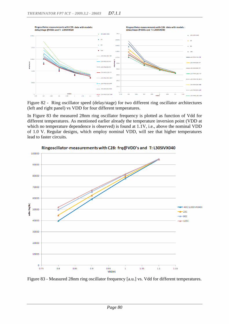
THERMINATOR FP7 ICT – 2009.3.2 - 28603 D7.1.1
Page 80
Figure 82 - Ring oscillator speed (delay/stage) for two different ring oscillator architectures
(left and right panel) vs VDD for four different temperatures.
In Figure 83 the measured 28nm ring oscillator frequency is plotted as function of Vdd for
different temperatures. As mentioned earlier already the temperature inversion point (VDD at
which no temperature dependence is observed) is found at 1.1V, i.e., above the nominal VDD
of 1.0 V. Regular designs, which employ nominal VDD, will see that higher temperatures
lead to faster circuits.
Figure 83 - Measured 28nm ring oscillator frequency [a.u.] vs. Vdd for different temperatures.

THERMINATOR FP7 ICT – 2009.3.2 - 28603 D7.1.1
Page 81
Figure 84 shows the relative difference between model and measurement data for 28nm ring
oscillator frequency as function of temperature at different VDDs. The new PSP methodology
exhibits a much smaller delta between measurements and simulation results than the previous
models. The pure temperature effect is very well reflected in the PSP models (solid lines
running predominantly horizontal, less than 2.5% delta, better than with previous
methodology, which resulted in up to 10% delta), and the overall PSP model accuracy, which
also covers VDD dependence and centering accuracy, is better than 8%.
Figure 84 - Relative difference between model and measurement data for 28nm ring oscillator
frequency vs. temperature at different VDDs. Dashed lines: previous, device-based
methodology, solid lines: advanced, circuit-referenced PSP models.
6.4 Conclusions
New modelling capabilities to support accurate thermal analysis and simulation have been
developed in the scope of WP1 and WP2. In this deliverable, models for advanced 40nm and
28nm technologies have been extracted and qualified with respect to hardware measurements
on both device and circuit level.
As a consequence of the gate stack changes and reduced nominal gate length, 28nm exhibits a
stronger temperature dependence between long and short devices than 40nm. Thus, an
accurate temperature modelling is becoming more important from 40nm to 28nm and with
further scaling.
In 28nm we have leveraged the advantage of employing a circuit-referenced temperature
modelling methodology with the local model approach of PSP to increase the model accuracy
over the full required geometry and temperature range. This novel PSP-methodology has lead

THERMINATOR FP7 ICT – 2009.3.2 - 28603 D7.1.1
Page 82
to a more accurate reflection of hardware behaviour than the previously used approach.
Therefore, respective temperature models have been rolled out as part of the full-custom as
well as semi-custom design flow to safeguard designs and to fulfil temperature specs of
advanced products. The improved models allow to control, manage and compensate thermally
induced effects on parameters such as timing and power; they positively impact reliability and
yield.
The models have been proven to provide good accuracy on test chips and reference designs.
As a consequence, they serve as basis for productive designs now.
The new circuit-referenced methodology exhibits smaller deltas between measurements and
simulation results than the previous models. The quantifiable objective “deviation between
measurement and model/simulation less than 20%” has been well achieved with ring
oscillator frequencies in both technologies, 28 and 40nm - showing an effective delta of about
+/- 2% over the whole temperature range of -40 to +125 °C.

THERMINATOR FP7 ICT – 2009.3.2 - 28603 D7.1.1
Page 83
7 TCAD of advanced and future MOSFETs
(FHG, together with IMC)
7.1.1 Introduction
In Task 2.1, reported in deliverable D2.1.4 [7], Fraunhofer IISB investigated the self-heating
of advanced SOI based MOSFETs and extracted compact models for a novel CMOS
generation envisaged by the ITRS for 2015. The results on self-heating of advanced CMOS
transistors were found to depend on the thermal conduction in the thin layers of silicon in
which the transistors are realized and in the other materials that surrounds them. In the novel
CMOS transistors, high-k-dielectrics are used instead of silicon dioxide. Also the CMOS
transistors of the newest technology generation with 28 nm gate length used by IMC in the
demonstrator circuits (Testcase 3) in this project have a gate isolation made from high-k-
dielectrics. Therefore, the effect of high-k-dielectrics, which are the choice for the gate
dielectrics for the future CMOS generations, on thermal properties of CMOS transistors had
to be investigated. The effect of high-k-dielectrics was studied here in Task 7.1 by means of
numerical simulation.
7.2 Impact of high-k gate isolation on temperature sensitivity of advanced
MOSFETs
Identical geometrical shape and doping can easily be realized in numerical simulations, so
that the effect of the material used for gate isolation can be studied separately from other
factors causing differences in the thermal behaviour. Since an evaluation of the future CMOS
technology generations is an important goal of this project, we took as an example of an
advanced CMOS future technology the SOI based CMOS technology generation specified by
the ITRS for 2015.
According to the ITRS [8], the gate length of CMOS transistors for 2015 will be 17 nm, the
silicon body thickness in fully-depleted single-gate SOI-based transistors 5.5 nm, the supply
voltage 0.81 V. We used the specifications of the 2009 version of the ITRS to allow a direct
comparison to the results of D2.1.4 where the same specifications were used. Since the active
area of SOI transistors is isolated from the silicon substrate by the buried silicon oxide layer, a
larger self-heating effect is expected in SOI transistors compared to their bulk silicon
counterparts. The upper part of the silicon body in SOI transistors is in an immediate thermal
contact to metallic source and drain contacts. However, the channel region in CMOS
transistors is separated from the metallic gate electrode by the thin gate isolation. While the
traditional gate isolation was made from silicon dioxide, high-k-dielectric materials are used
as gate isolation in novel CMOS technology nodes. Hafnium dioxide, HfO2, is a typical high-
k-dielectric used in advanced CMOS transistors and we used this high-k-material in our
simulations as an example of high-k-gate dielectrics. To separate specific effects induced by
HfO2 from other possible influences associated with the size of transistor elements and with
the doping, completely identical sizes and doping of the devices were used except for the
physical thickness of the gate dielectrics. To ensure as close as possible similarity of electrical
performance of the devices under comparison, equal effective electrical thickness of silicon
dioxide and of HfO2 gate dielectrics was chosen. In both variants of the simulation, the
effective gate oxide thickness, which is the thickness of the standard silicon dioxide that gives
the same electrical capacitance as the capacitance of the high-k-isolated capacitor, was
0.53 nm, as specified by ITRS [8]. This value of the effective gate oxide thickness does not
include the effect of quantum-mechanical depletion of the charge carriers near the silicon-to-
gate-isolation interface. The effects of quantum depletion will be accounted for in the
electrical device simulations presented below. The geometrical shape of the simulated SOI
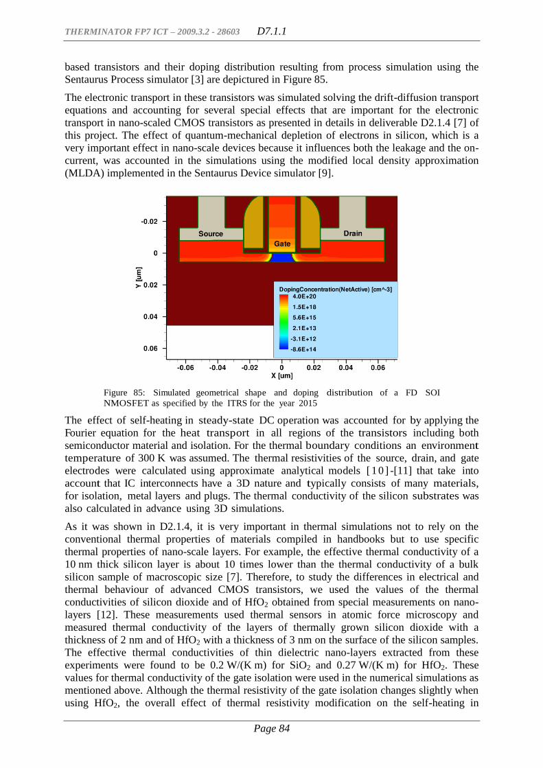
THERMINATOR FP7 ICT – 2009.3.2 - 28603 D7.1.1
Page 84
based transistors and their doping distribution resulting from process simulation using the
Sentaurus Process simulator [3] are depictured in Figure 85.
The electronic transport in these transistors was simulated solving the drift-diffusion transport
equations and accounting for several special effects that are important for the electronic
transport in nano-scaled CMOS transistors as presented in details in deliverable D2.1.4 [7] of
this project. The effect of quantum-mechanical depletion of electrons in silicon, which is a
very important effect in nano-scale devices because it influences both the leakage and the on-
current, was accounted in the simulations using the modified local density approximation
(MLDA) implemented in the Sentaurus Device simulator [9].
Figure 85: Simulated geometrical shape and doping distribution of a FD SOI
NMOSFET as specified by the ITRS for the year 2015
The effect of self-heating in steady-state DC operation was accounted for by applying the
Fourier equation for the heat transport in all regions of the transistors including both
semiconductor material and isolation. For the thermal boundary conditions an environment
temperature of 300 K was assumed. The thermal resistivities of the source, drain, and gate
electrodes were calculated using approximate analytical models [ 10 ] -[11] that take into
account that IC interconnects have a 3D nature and typically consists of many materials,
for isolation, metal layers and plugs. The thermal conductivity of the silicon substrates was
also calculated in advance using 3D simulations.
As it was shown in D2.1.4, it is very important in thermal simulations not to rely on the
conventional thermal properties of materials compiled in handbooks but to use specific
thermal properties of nano-scale layers. For example, the effective thermal conductivity of a
10 nm thick silicon layer is about 10 times lower than the thermal conductivity of a bulk
silicon sample of macroscopic size [7]. Therefore, to study the differences in electrical and
thermal behaviour of advanced CMOS transistors, we used the values of the thermal
conductivities of silicon dioxide and of HfO2 obtained from special measurements on nano-
layers [12]. These measurements used thermal sensors in atomic force microscopy and
measured thermal conductivity of the layers of thermally grown silicon dioxide with a
thickness of 2 nm and of HfO2 with a thickness of 3 nm on the surface of the silicon samples.
The effective thermal conductivities of thin dielectric nano-layers extracted from these
experiments were found to be 0.2 W/(K m) for SiO2 and 0.27 W/(K m) for HfO2. These
values for thermal conductivity of the gate isolation were used in the numerical simulations as
mentioned above. Although the thermal resistivity of the gate isolation changes slightly when
using HfO2, the overall effect of thermal resistivity modification on the self-heating in
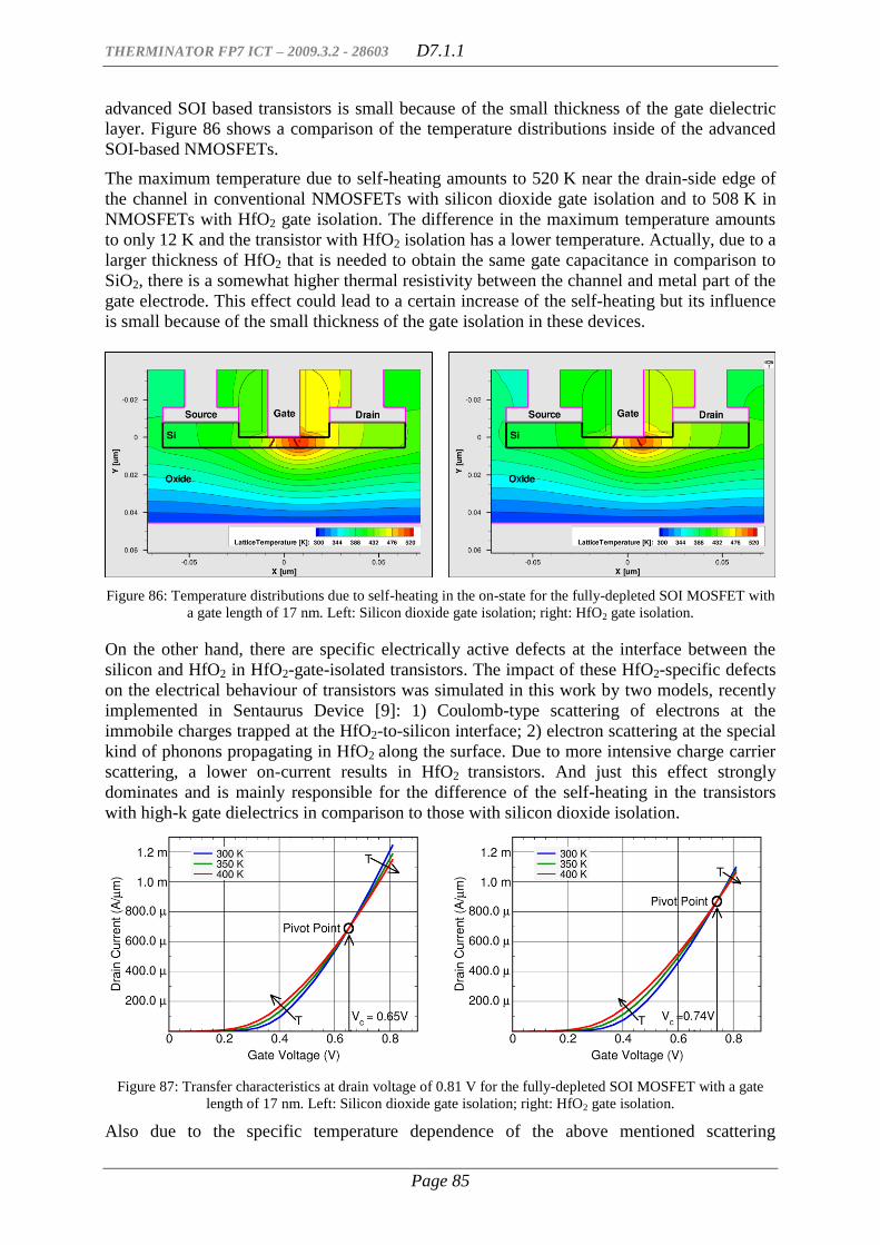
THERMINATOR FP7 ICT – 2009.3.2 - 28603 D7.1.1
Page 85
advanced SOI based transistors is small because of the small thickness of the gate dielectric
layer. Figure 86 shows a comparison of the temperature distributions inside of the advanced
SOI-based NMOSFETs.
The maximum temperature due to self-heating amounts to 520 K near the drain-side edge of
the channel in conventional NMOSFETs with silicon dioxide gate isolation and to 508 K in
NMOSFETs with HfO2 gate isolation. The difference in the maximum temperature amounts
to only 12 K and the transistor with HfO2 isolation has a lower temperature. Actually, due to a
larger thickness of HfO2 that is needed to obtain the same gate capacitance in comparison to
SiO2, there is a somewhat higher thermal resistivity between the channel and metal part of the
gate electrode. This effect could lead to a certain increase of the self-heating but its influence
is small because of the small thickness of the gate isolation in these devices.
Figure 86: Temperature distributions due to self-heating in the on-state for the fully-depleted SOI MOSFET with
a gate length of 17 nm. Left: Silicon dioxide gate isolation; right: HfO2 gate isolation.
On the other hand, there are specific electrically active defects at the interface between the
silicon and HfO2 in HfO2-gate-isolated transistors. The impact of these HfO2-specific defects
on the electrical behaviour of transistors was simulated in this work by two models, recently
implemented in Sentaurus Device [9]: 1) Coulomb-type scattering of electrons at the
immobile charges trapped at the HfO2-to-silicon interface; 2) electron scattering at the special
kind of phonons propagating in HfO2 along the surface. Due to more intensive charge carrier
scattering, a lower on-current results in HfO2 transistors. And just this effect strongly
dominates and is mainly responsible for the difference of the self-heating in the transistors
with high-k gate dielectrics in comparison to those with silicon dioxide isolation.
Figure 87: Transfer characteristics at drain voltage of 0.81 V for the fully-depleted SOI MOSFET with a gate
length of 17 nm. Left: Silicon dioxide gate isolation; right: HfO2 gate isolation.
Also due to the specific temperature dependence of the above mentioned scattering
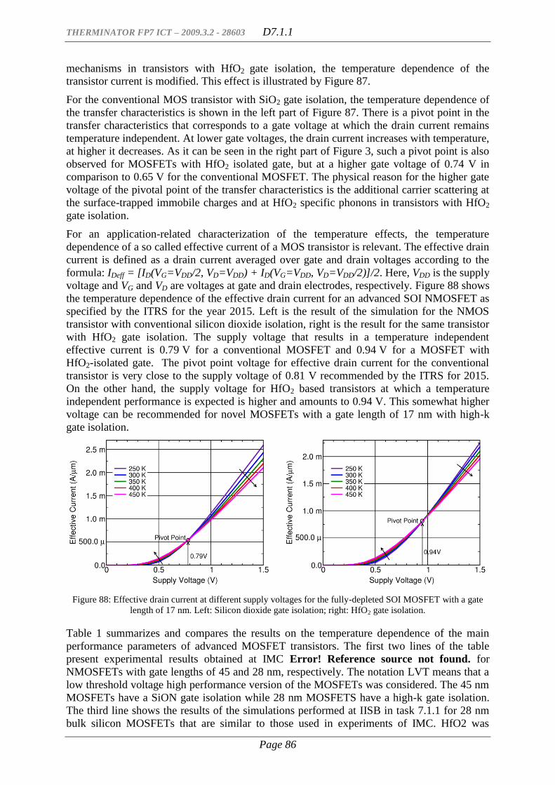
THERMINATOR FP7 ICT – 2009.3.2 - 28603 D7.1.1
Page 86
mechanisms in transistors with HfO2 gate isolation, the temperature dependence of the
transistor current is modified. This effect is illustrated by Figure 87.
For the conventional MOS transistor with SiO2 gate isolation, the temperature dependence of
the transfer characteristics is shown in the left part of Figure 87. There is a pivot point in the
transfer characteristics that corresponds to a gate voltage at which the drain current remains
temperature independent. At lower gate voltages, the drain current increases with temperature,
at higher it decreases. As it can be seen in the right part of Figure 3, such a pivot point is also
observed for MOSFETs with HfO2 isolated gate, but at a higher gate voltage of 0.74 V in
comparison to 0.65 V for the conventional MOSFET. The physical reason for the higher gate
voltage of the pivotal point of the transfer characteristics is the additional carrier scattering at
the surface-trapped immobile charges and at HfO2 specific phonons in transistors with HfO2
gate isolation.
For an application-related characterization of the temperature effects, the temperature
dependence of a so called effective current of a MOS transistor is relevant. The effective drain
current is defined as a drain current averaged over gate and drain voltages according to the
formula: IDeff = [ID(VG=VDD/2, VD=VDD) + ID(VG=VDD, VD=VDD/2)]/2. Here, VDD is the supply
voltage and VG and VD are voltages at gate and drain electrodes, respectively. Figure 88 shows
the temperature dependence of the effective drain current for an advanced SOI NMOSFET as
specified by the ITRS for the year 2015. Left is the result of the simulation for the NMOS
transistor with conventional silicon dioxide isolation, right is the result for the same transistor
with HfO2 gate isolation. The supply voltage that results in a temperature independent
effective current is 0.79 V for a conventional MOSFET and 0.94 V for a MOSFET with
HfO2-isolated gate. The pivot point voltage for effective drain current for the conventional
transistor is very close to the supply voltage of 0.81 V recommended by the ITRS for 2015.
On the other hand, the supply voltage for HfO2 based transistors at which a temperature
independent performance is expected is higher and amounts to 0.94 V. This somewhat higher
voltage can be recommended for novel MOSFETs with a gate length of 17 nm with high-k
gate isolation.
Figure 88: Effective drain current at different supply voltages for the fully-depleted SOI MOSFET with a gate
length of 17 nm. Left: Silicon dioxide gate isolation; right: HfO2 gate isolation.
Table 1 summarizes and compares the results on the temperature dependence of the main
performance parameters of advanced MOSFET transistors. The first two lines of the table
present experimental results obtained at IMC Error! Reference source not found. for
NMOSFETs with gate lengths of 45 and 28 nm, respectively. The notation LVT means that a
low threshold voltage high performance version of the MOSFETs was considered. The 45 nm
MOSFETs have a SiON gate isolation while 28 nm MOSFETS have a high-k gate isolation.
The third line shows the results of the simulations performed at IISB in task 7.1.1 for 28 nm
bulk silicon MOSFETs that are similar to those used in experiments of IMC. HfO2 was

THERMINATOR FP7 ICT – 2009.3.2 - 28603 D7.1.1
Page 87
assumed as gate isolation material in these simulations and the same simulation models as
presented before for 17 nm SOI transistors were used. The two last lines present the
simulation results of Fraunhofer IISB for the 17 nm gate length fully-depleted SOI-based n-
channel MOSFETs. The third line is for conventional silicon dioxide gate isolation and the
last, fourth, line is for the same kind of transistor but with a HfO2 gate isolation.
Three temperature-related parameters that describe the evolution of the performance of the
transistors with temperature are tabulated. The first parameter is the Vtsat Temperature
Coefficient (VTC). This coefficient characterizes how much the threshold voltage of the
transistors changes when the temperature increases by 1 K. Negative values mean that the
threshold voltage lowers when the temperature increases. It is interesting to note that the VTC
for novel 17 nm SOI based transistors with the traditional silicon dioxide isolation is equal to
the VTC of 45 nm bulk silicon MOSFETs. Such a good agreement in the VTC for transistors
with different gate lengths is expected because the VTC parameter is mainly determined by
the silicon properties and the impact of the interface-located defects on scattering of the
charge carriers is negligible in these transistors. In contrast, both transistors with high-k-gate-
isolation exhibit somewhat higher values of VTC.
Table 1: Temperature sensitivity parameters for advanced NMOSFETs
Device Type Gate
Isolatio
n
Gate
Length
(nm)
Vtsat Tempera-
ture Coefficient
(mV/K)
On-Current
Temperature
Coefficient
(%/100K)
Eff. Current
Temperature
Coefficient
(%/100K)
LVT NFET
Error!
Reference
source not
found.
SiON 45 -0.47 -5.88 -2.4
LVT NFET [5] High-k 28 -0.65 -2.35 1.2
LVT NFET Sim. HfO2 28 -0.52 -3.39 1.75
FD SOI NFET SiO2 17 -0.47 -4.50 -1.05
FD SOI NFET HfO2 17 -0.49 -1.73 5.98
The second temperature-related parameter is the on-current temperature coefficient (OCTC)
and shows how much the on-current changes when the temperature increases by 100 K. This
coefficient takes typically negative values and reflects the degradation of the charge carrier
mobility due to the increase of scattering at thermal vibrations with increasing temperature.
Comparing the oxide-isolated and high-k-isolated gates we observe that transistors with high-
k-isolated gates have significantly lower absolute values of the on-current temperature
coefficient. There is also a slight reduction of the absolute value of this coefficient with a
reduction of the gate length, compare lines 2 and 5 of Table 1. This can be explained by the
fact that in transistors with shorter gate length the relative role of the parasitic resistances,
which are essentially temperature independent, increases. Observing this we can conclude that
the effect of the on-current degradation with temperature diminishes for the future generations
of CMOS transistors, partly because of shorter gate lengths and partly because of the high-k-
dielectrics.
The third temperature-related parameter is the temperature coefficient for the effective drain
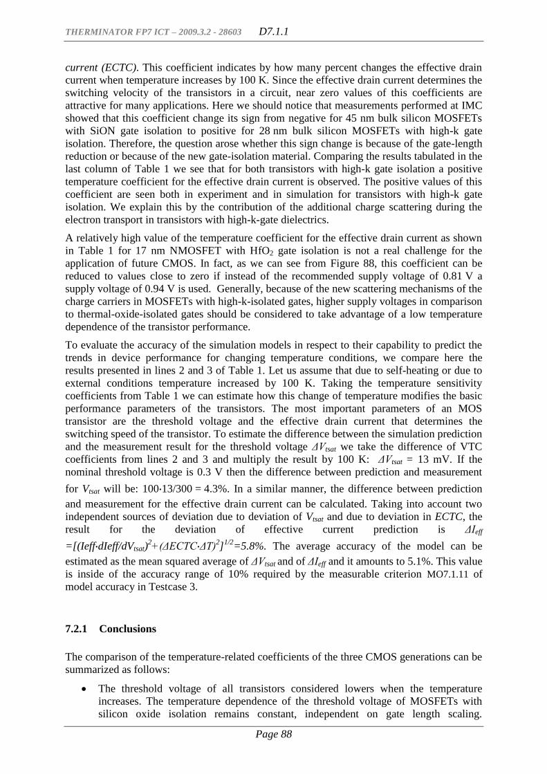
THERMINATOR FP7 ICT – 2009.3.2 - 28603 D7.1.1
Page 88
current (ECTC). This coefficient indicates by how many percent changes the effective drain
current when temperature increases by 100 K. Since the effective drain current determines the
switching velocity of the transistors in a circuit, near zero values of this coefficients are
attractive for many applications. Here we should notice that measurements performed at IMC
showed that this coefficient change its sign from negative for 45 nm bulk silicon MOSFETs
with SiON gate isolation to positive for 28 nm bulk silicon MOSFETs with high-k gate
isolation. Therefore, the question arose whether this sign change is because of the gate-length
reduction or because of the new gate-isolation material. Comparing the results tabulated in the
last column of Table 1 we see that for both transistors with high-k gate isolation a positive
temperature coefficient for the effective drain current is observed. The positive values of this
coefficient are seen both in experiment and in simulation for transistors with high-k gate
isolation. We explain this by the contribution of the additional charge scattering during the
electron transport in transistors with high-k-gate dielectrics.
A relatively high value of the temperature coefficient for the effective drain current as shown
in Table 1 for 17 nm NMOSFET with HfO2 gate isolation is not a real challenge for the
application of future CMOS. In fact, as we can see from Figure 88, this coefficient can be
reduced to values close to zero if instead of the recommended supply voltage of 0.81 V a
supply voltage of 0.94 V is used. Generally, because of the new scattering mechanisms of the
charge carriers in MOSFETs with high-k-isolated gates, higher supply voltages in comparison
to thermal-oxide-isolated gates should be considered to take advantage of a low temperature
dependence of the transistor performance.
To evaluate the accuracy of the simulation models in respect to their capability to predict the
trends in device performance for changing temperature conditions, we compare here the
results presented in lines 2 and 3 of Table 1. Let us assume that due to self-heating or due to
external conditions temperature increased by 100 K. Taking the temperature sensitivity
coefficients from Table 1 we can estimate how this change of temperature modifies the basic
performance parameters of the transistors. The most important parameters of an MOS
transistor are the threshold voltage and the effective drain current that determines the
switching speed of the transistor. To estimate the difference between the simulation prediction
and the measurement result for the threshold voltage ΔVtsat we take the difference of VTC
coefficients from lines 2 and 3 and multiply the result by 100 K: ΔVtsat = 13 mV. If the
nominal threshold voltage is 0.3 V then the difference between prediction and measurement
for Vtsat will be: 100⋅13/300 = 4.3%. In a similar manner, the difference between prediction
and measurement for the effective drain current can be calculated. Taking into account two
independent sources of deviation due to deviation of Vtsat and due to deviation in ECTC, the
result for the deviation of effective current prediction is ΔIeff
=[(Ieff⋅dIeff/dVtsat)2+(ΔECTC⋅ΔT)
2]
1/2=5.8%. The average accuracy of the model can be
estimated as the mean squared average of ΔVtsat and of ΔIeff and it amounts to 5.1%. This value
is inside of the accuracy range of 10% required by the measurable criterion MO7.1.11 of
model accuracy in Testcase 3.
7.2.1 Conclusions
The comparison of the temperature-related coefficients of the three CMOS generations can be
summarized as follows:
The threshold voltage of all transistors considered lowers when the temperature
increases. The temperature dependence of the threshold voltage of MOSFETs with
silicon oxide isolation remains constant, independent on gate length scaling.
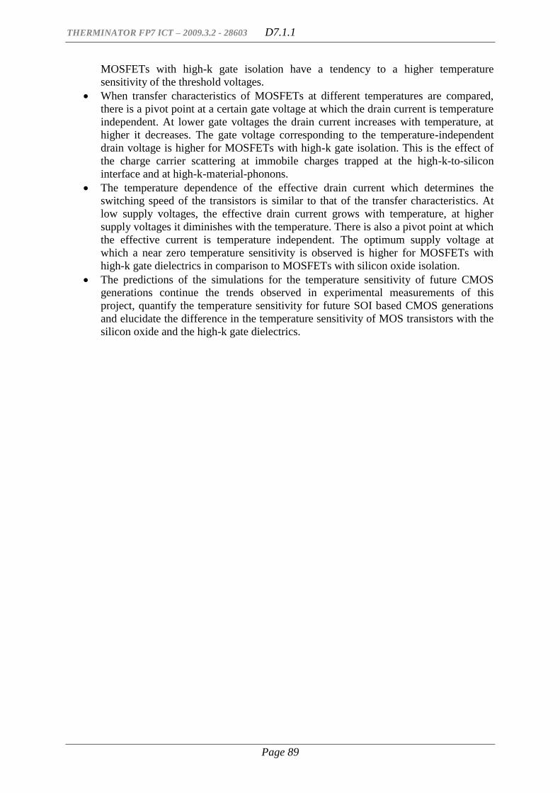
THERMINATOR FP7 ICT – 2009.3.2 - 28603 D7.1.1
Page 89
MOSFETs with high-k gate isolation have a tendency to a higher temperature
sensitivity of the threshold voltages.
When transfer characteristics of MOSFETs at different temperatures are compared,
there is a pivot point at a certain gate voltage at which the drain current is temperature
independent. At lower gate voltages the drain current increases with temperature, at
higher it decreases. The gate voltage corresponding to the temperature-independent
drain voltage is higher for MOSFETs with high-k gate isolation. This is the effect of
the charge carrier scattering at immobile charges trapped at the high-k-to-silicon
interface and at high-k-material-phonons.
The temperature dependence of the effective drain current which determines the
switching speed of the transistors is similar to that of the transfer characteristics. At
low supply voltages, the effective drain current grows with temperature, at higher
supply voltages it diminishes with the temperature. There is also a pivot point at which
the effective current is temperature independent. The optimum supply voltage at
which a near zero temperature sensitivity is observed is higher for MOSFETs with
high-k gate dielectrics in comparison to MOSFETs with silicon oxide isolation.
The predictions of the simulations for the temperature sensitivity of future CMOS
generations continue the trends observed in experimental measurements of this
project, quantify the temperature sensitivity for future SOI based CMOS generations
and elucidate the difference in the temperature sensitivity of MOS transistors with the
silicon oxide and the high-k gate dielectrics.

THERMINATOR FP7 ICT – 2009.3.2 - 28603 D7.1.1
Page 90
8 DC and AC thermal-characterization of FinFETs (UNIBO)
8.1 Introduction
This part of the deliverable compares the results of numerical device simulations
accounting for self-heating, with the results of experimental DC and AC characterization
of small geometry MOSFETs. This activity is performed within WP7, with the aim to
confirm the accuracy of the simulation procedure developed by UNIBO in the frame of
WP2, and applied to the analysis of the impact of self-heating on the figures of merit for
AC and digital operation [13]; our declared measurable objective MO7.1.12 is a 10%
maximum deviation between the results of simulations and available experimental data.
In particular, we present detailed DC and AC numerical simulations of thermal effects in
nano-scale FinFET devices. Three–dimensional electro–thermal numerical simulations,
including a realistic description of the source, drain and gate interconnections, are
validated by comparison with experimental DC I–V and AC small–signal parameters. The
importance of a realistic description of interconnect in AC simulations of FinFETs is
discussed. The large frequency dispersion of AC parameters, suggests small signal
analysis as a powerful method for the experimental characterization of self-heating
effects, particularly in the case of low-power devices, for which the sensitivity of DC I-V
curves to thermal effects is rather small.
8.2 Simulated devices
N–channel FinFET devices have been simulated using the Sentaurus device simulator[14];
the results obtained from measurements performed on similar devices are presented and
widely discussed in [15].
Three different gate lengths have been considered: LG=1 μm, 190 nm and 70 nm. The
main characteristics of the simulated transistors are listed in Table 2.
Table 2- Key parameters of the nominal device
The gate oxide thickness is uniform for the lateral gates and for the top gate; an abrupt
junction is assumed between the S/D regions and the substrate. The device is covered by a
SiO2 passivation layer, whose thickness tPAS is kept constant and equal to 200 nm.
Beneath the BOX, a 1.8 μm thick Silicon layer is included in the simulation.
From a thermal point of view, the temperature distribution inside the transistor is a
function of the fin position, the inner fins being hotter than the peripheral ones. In our
case, the simulated structure is representative of an inner fin. Regarding the thermal

THERMINATOR FP7 ICT – 2009.3.2 - 28603 D7.1.1
Page 91
boundary conditions that have been adopted in our simulations, the source, drain and gate
interconnects have been defined as metal wires; in particular, source and drain are
designed as copper wires, featuring rectangular cross section and a length equal to the
healing length, which is the characteristic length for exponential temperature attenuation
due to heat exchange with the ideal sink through the insulator–semiconductor stack [16].
At the end of such wires, a 300 K isothermal boundary condition is set. These wires act as
cooling fins, exchanging heat in the vertical direction, toward the substrate heat sink,
through a stack of inter–metal insulator, BOX, and silicon substrate. Finally, the gate
contact has been modeled as a poly-silicon wire, whose length is limited by the inter–fins
distance ( fin , see Table 2).
Figure 89 presents a simple sketch of the “intrinsic” simulated device: the interconnect is
not shown. In Figure 90a, 2D-section of the whole simulation domain is described,
including the metal wires, the passivation layer as well as the inter–metal dielectrics
(IMD).
In order to correctly match the experimental data, parasitic series resistances have been
added to the S/D contacts (RS/D=11.8 kW ); moreover, the saturation velocity parameters
have been calibrated for very short devices in order to account for velocity overshoot,
according to the approach suggested by Bude[17]. Table 3 reports the values adopted for
the different structures.
3D E–T simulations require a large computational burden, in terms of CPU time and
allocated memory: in order to perform feasible tasks, quantum corrections are not taken
into account.
Moreover, in order to minimize the node count of the structures, the simulation domain is
one–half of the complete transistor (i.e. only Wfin/2 is considered). This is possible by
exploiting the symmetries of the simulated structures. The silicon thermal conductivity Si
is treated as a decreasing function of film thickness and temperature according to the
model proposed by Liu[18]. Moreover, the thermal conductivity of the gate oxide has
been calibrated in order to take into account for surface effects at both the silicon–
dielectric and dielectric–gate interfaces.
Figure 89-Simple sketch of the simulated FinFET. The does no show the metallization
lines, and it is not in scale.

THERMINATOR FP7 ICT – 2009.3.2 - 28603 D7.1.1
Page 92
Figure 90- Cross section along the x-y plain of the whole simulation domain: the figure is
not in scale. The yellow dashed—contoured region is the intrinsic FinFET (see Figure 89)
Table 3 – Saturation velocity values adopted for the transistor under analysis.
8.3 Model verification
In order to validate our model, we compared the DC output characteristics: Figure 91-
Figure 93 show the IDS–VDS curves for the considered structures and for different VGS
values. The simulation results are in good agreement with the experiments, for the whole
range of the considered LG, demonstrating the achievement of the measurable objective of
10% maximum deviation of electro-thermal simulations with respect to experimental data.
Figure 91 – IDS-VDS characteristics for the 1m gate length device, for different VGS.
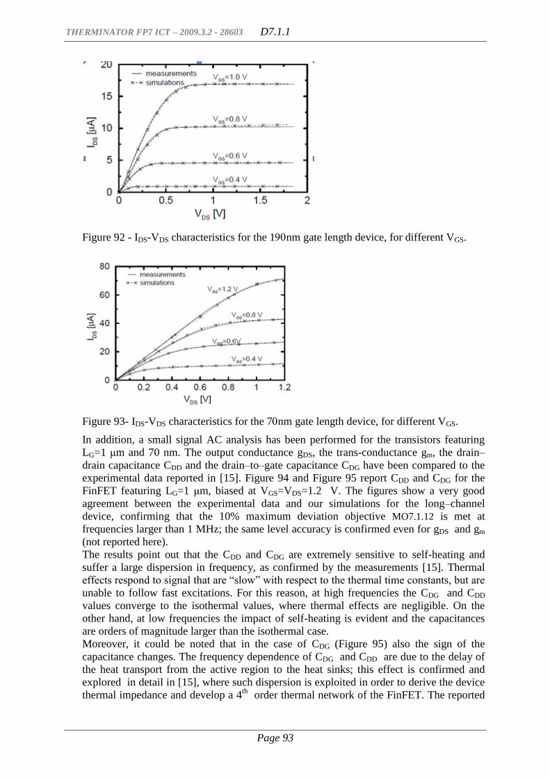
THERMINATOR FP7 ICT – 2009.3.2 - 28603 D7.1.1
Page 93
Figure 92 - IDS-VDS characteristics for the 1nm gate length device, for different VGS.
Figure 93- IDS-VDS characteristics for the 7nm gate length device, for different VGS.
In addition, a small signal AC analysis has been performed for the transistors featuring
LG=1 μm and 70 nm. The output conductance gDS, the trans-conductance gm, the drain–
drain capacitance CDD and the drain–to–gate capacitance CDG have been compared to the
experimental data reported in [15]. Figure 94 and Figure 95 report CDD and CDG for the
FinFET featuring LG=1 μm, biased at VGS=VDS=1.2 V. The figures show a very good
agreement between the experimental data and our simulations for the long–channel
device, confirming that the 10% maximum deviation objective MO7.1.12 is met at
frequencies larger than 1 MHz; the same level accuracy is confirmed even for gDS and gm
(not reported here).
The results point out that the CDD and CDG are extremely sensitive to self-heating and
suffer a large dispersion in frequency, as confirmed by the measurements [15]. Thermal
effects respond to signal that are “slow” with respect to the thermal time constants, but are
unable to follow fast excitations. For this reason, at high frequencies the CDG and CDD
values converge to the isothermal values, where thermal effects are negligible. On the
other hand, at low frequencies the impact of self-heating is evident and the capacitances
are orders of magnitude larger than the isothermal case.
Moreover, it could be noted that in the case of CDG (Figure 95) also the sign of the
capacitance changes. The frequency dependence of CDG and CDD are due to the delay of
the heat transport from the active region to the heat sinks; this effect is confirmed and
explored in detail in [15], where such dispersion is exploited in order to derive the device
thermal impedance and develop a 4th
order thermal network of the FinFET. The reported
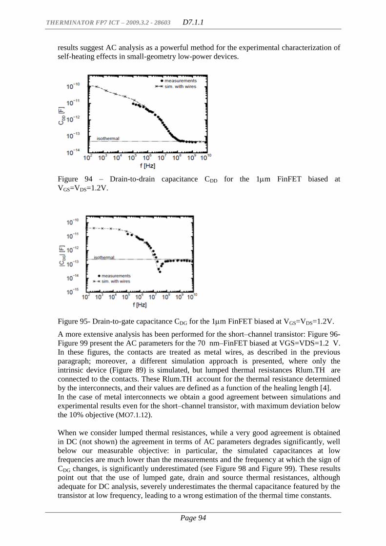
THERMINATOR FP7 ICT – 2009.3.2 - 28603 D7.1.1
Page 94
results suggest AC analysis as a powerful method for the experimental characterization of
self-heating effects in small-geometry low-power devices.
Figure 94 – Drain-to-drain capacitance CDD for the 1m FinFET biased at
VGS=VDS=1.2V.
Figure 95- Drain-to-gate capacitance CDG for the 1m FinFET biased at VGS=VDS=1.2V.
A more extensive analysis has been performed for the short–channel transistor: Figure 96-
Figure 99 present the AC parameters for the 70 nm–FinFET biased at VGS=VDS=1.2 V.
In these figures, the contacts are treated as metal wires, as described in the previous
paragraph; moreover, a different simulation approach is presented, where only the
intrinsic device (Figure 89) is simulated, but lumped thermal resistances Rlum.TH are
connected to the contacts. These Rlum.TH account for the thermal resistance determined
by the interconnects, and their values are defined as a function of the healing length [4].
In the case of metal interconnects we obtain a good agreement between simulations and
experimental results even for the short–channel transistor, with maximum deviation below
the 10% objective (MO7.1.12).
When we consider lumped thermal resistances, while a very good agreement is obtained
in DC (not shown) the agreement in terms of AC parameters degrades significantly, well
below our measurable objective: in particular, the simulated capacitances at low
frequencies are much lower than the measurements and the frequency at which the sign of
CDG changes, is significantly underestimated (see Figure 98 and Figure 99). These results
point out that the use of lumped gate, drain and source thermal resistances, although
adequate for DC analysis, severely underestimates the thermal capacitance featured by the
transistor at low frequency, leading to a wrong estimation of the thermal time constants.
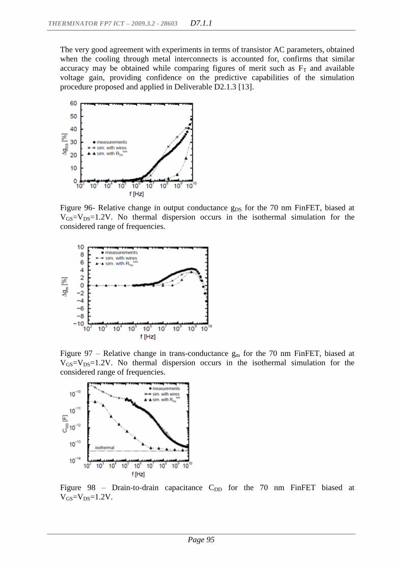
THERMINATOR FP7 ICT – 2009.3.2 - 28603 D7.1.1
Page 95
The very good agreement with experiments in terms of transistor AC parameters, obtained
when the cooling through metal interconnects is accounted for, confirms that similar
accuracy may be obtained while comparing figures of merit such as FT and available
voltage gain, providing confidence on the predictive capabilities of the simulation
procedure proposed and applied in Deliverable D2.1.3 [13].
Figure 96- Relative change in output conductance gDS for the 70 nm FinFET, biased at
VGS=VDS=1.2V. No thermal dispersion occurs in the isothermal simulation for the
considered range of frequencies.
Figure 97 – Relative change in trans-conductance gm for the 70 nm FinFET, biased at
VGS=VDS=1.2V. No thermal dispersion occurs in the isothermal simulation for the
considered range of frequencies.
Figure 98 – Drain-to-drain capacitance CDD for the 70 nm FinFET biased at
VGS=VDS=1.2V.

THERMINATOR FP7 ICT – 2009.3.2 - 28603 D7.1.1
Page 96
Figure 99- Drain-to-gate capacitance CDG for the 70 nm FinFET biased at VGS=VDS=1.2V.
8.4 Conclusions
In this part of the deliverable, we performed realistic numerical electro–thermal
simulations of FinFETs, including the source, drain and gate interconnects, in order to
analyze the impact of self–heating both on DC I–V characteristics and small–signal AC
parameters, with the aim to confirm the achievement of our 10% maximum deviation with
respect to experimental data.
Our analysis pointed out that a “simple” approach consisting of lumped thermal
resistances severely underestimates the CDD and CDG capacitances at low frequencies, and
therefore the correct thermal capacitance associated to the transistor.
In conclusion, a detailed modelling of the metal interconnection wires is essential for AC
analysis.
A correct modelling of device cooling through metal interconnects allows to achieve the
10% maximum deviation, representing the objective (MO7.1.12) of our simulation activity
within Therminator.
The reported results put in evidence that AC characterization, thanks to the large
sensitivity of capacitance parameters to thermal effects, emphasized by the change in sign
of CDG, represents a more powerful approach to the analysis of self-heating in low-power
devices, than conventional ones based on I-V curves and pulsed measurements.
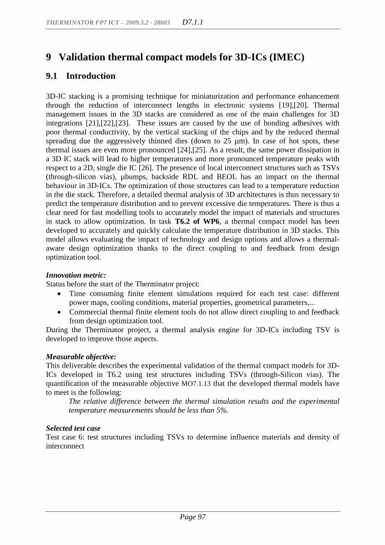
THERMINATOR FP7 ICT – 2009.3.2 - 28603 D7.1.1
Page 97
9 Validation thermal compact models for 3D-ICs (IMEC)
9.1 Introduction
3D-IC stacking is a promising technique for miniaturization and performance enhancement
through the reduction of interconnect lengths in electronic systems [19],[20]. Thermal
management issues in the 3D stacks are considered as one of the main challenges for 3D
integrations [21],[22],[23]. These issues are caused by the use of bonding adhesives with
poor thermal conductivity, by the vertical stacking of the chips and by the reduced thermal
spreading due the aggressively thinned dies (down to 25 µm). In case of hot spots, these
thermal issues are even more pronounced [24],[25]. As a result, the same power dissipation in
a 3D IC stack will lead to higher temperatures and more pronounced temperature peaks with
respect to a 2D, single die IC [26]. The presence of local interconnect structures such as TSVs
(through-silicon vias), µbumps, backside RDL and BEOL has an impact on the thermal
behaviour in 3D-ICs. The optimization of those structures can lead to a temperature reduction
in the die stack. Therefore, a detailed thermal analysis of 3D architectures is thus necessary to
predict the temperature distribution and to prevent excessive die temperatures. There is thus a
clear need for fast modelling tools to accurately model the impact of materials and structures
in stack to allow optimization. In task T6.2 of WP6, a thermal compact model has been
developed to accurately and quickly calculate the temperature distribution in 3D stacks. This
model allows evaluating the impact of technology and design options and allows a thermal-
aware design optimization thanks to the direct coupling to and feedback from design
optimization tool.
Innovation metric:
Status before the start of the Therminator project:
Time consuming finite element simulations required for each test case: different
power maps, cooling conditions, material properties, geometrical parameters,...
Commercial thermal finite element tools do not allow direct coupling to and feedback
from design optimization tool.
During the Therminator project, a thermal analysis engine for 3D-ICs including TSV is
developed to improve those aspects.
Measurable objective:
This deliverable describes the experimental validation of the thermal compact models for 3D-
ICs developed in T6.2 using test structures including TSVs (through-Silicon vias). The
quantification of the measurable objective MO7.1.13 that the developed thermal models have
to meet is the following:
The relative difference between the thermal simulation results and the experimental
temperature measurements should be less than 5%.
Selected test case
Test case 6: test structures including TSVs to determine influence materials and density of
interconnect
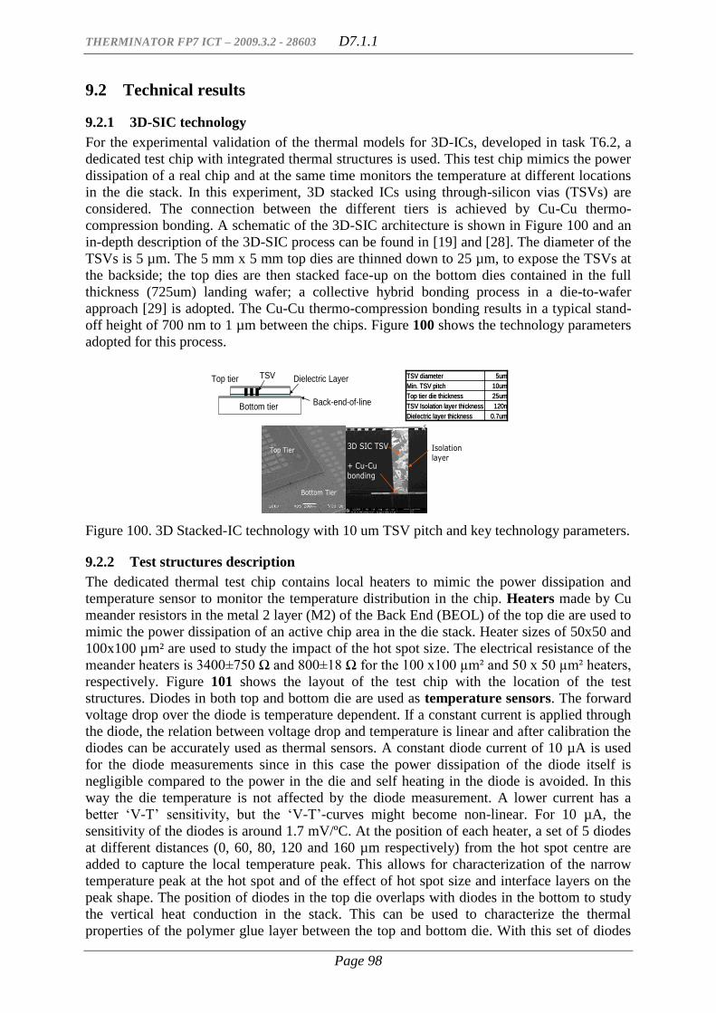
THERMINATOR FP7 ICT – 2009.3.2 - 28603 D7.1.1
Page 98
9.2 Technical results
9.2.1 3D-SIC technology
For the experimental validation of the thermal models for 3D-ICs, developed in task T6.2, a
dedicated test chip with integrated thermal structures is used. This test chip mimics the power
dissipation of a real chip and at the same time monitors the temperature at different locations
in the die stack. In this experiment, 3D stacked ICs using through-silicon vias (TSVs) are
considered. The connection between the different tiers is achieved by Cu-Cu thermo-
compression bonding. A schematic of the 3D-SIC architecture is shown in Figure 100 and an
in-depth description of the 3D-SIC process can be found in [19] and [28]. The diameter of the
TSVs is 5 µm. The 5 mm x 5 mm top dies are thinned down to 25 µm, to expose the TSVs at
the backside; the top dies are then stacked face-up on the bottom dies contained in the full
thickness (725um) landing wafer; a collective hybrid bonding process in a die-to-wafer
approach [29] is adopted. The Cu-Cu thermo-compression bonding results in a typical stand-
off height of 700 nm to 1 µm between the chips. Figure 100 shows the technology parameters
adopted for this process.
Figure 100. 3D Stacked-IC technology with 10 um TSV pitch and key technology parameters.
9.2.2 Test structures description
The dedicated thermal test chip contains local heaters to mimic the power dissipation and
temperature sensor to monitor the temperature distribution in the chip. Heaters made by Cu
meander resistors in the metal 2 layer (M2) of the Back End (BEOL) of the top die are used to
mimic the power dissipation of an active chip area in the die stack. Heater sizes of 50x50 and
100x100 µm² are used to study the impact of the hot spot size. The electrical resistance of the
meander heaters is 3400±750 Ω and 800±18 Ω for the 100 x100 µm² and 50 x 50 µm² heaters,
respectively. Figure 101 shows the layout of the test chip with the location of the test
structures. Diodes in both top and bottom die are used as temperature sensors. The forward
voltage drop over the diode is temperature dependent. If a constant current is applied through
the diode, the relation between voltage drop and temperature is linear and after calibration the
diodes can be accurately used as thermal sensors. A constant diode current of 10 µA is used
for the diode measurements since in this case the power dissipation of the diode itself is
negligible compared to the power in the die and self heating in the diode is avoided. In this
way the die temperature is not affected by the diode measurement. A lower current has a
better ‘V-T’ sensitivity, but the ‘V-T’-curves might become non-linear. For 10 µA, the
sensitivity of the diodes is around 1.7 mV/ºC. At the position of each heater, a set of 5 diodes
at different distances (0, 60, 80, 120 and 160 µm respectively) from the hot spot centre are
added to capture the local temperature peak. This allows for characterization of the narrow
temperature peak at the hot spot and of the effect of hot spot size and interface layers on the
peak shape. The position of diodes in the top die overlaps with diodes in the bottom to study
the vertical heat conduction in the stack. This can be used to characterize the thermal
properties of the polymer glue layer between the top and bottom die. With this set of diodes
3D SIC TSV
+ Cu-Cu bonding
Bottom Tier
Top Tier
Bottom tier
Top tier TSV Dielectric Layer
Back-end-of-line120nTSV Isolation layer thickness
0.7umDielectric layer thickness
25umTop tier die thickness
10umMin. TSV pitch
5umTSV diameter
120nTSV Isolation layer thickness
0.7umDielectric layer thickness
25umTop tier die thickness
10umMin. TSV pitch
5umTSV diameter
Isolationlayer

THERMINATOR FP7 ICT – 2009.3.2 - 28603 D7.1.1
Page 99
and heaters both the horizontal and vertical heat spreading in the stack can be accurately
studied.
Figure 101. Thermal test chip layout with 6 test structures: 2 heater dimensions and 3 TSV
densities.
Structures with TSV arrays of different densities below the heaters are also available to
characterize the potential TSV capability to locally enhance the heat transfer; in particular,
arrays of 7x7 TSVs (5%) and 11x11 TSVs (12%) are available together with a reference
structure without TSVs. The test die contains in total 6 thermal test modules that represent a
combination of 2 heater sizes and 3 TSV densities). Figure 102 gives an overview of the
location of these 6 modules on the test chip. Figure 102 (a) shows a schematic representation
of the cross-section of the test structures. In Figure 102(b), a detail of the layout at the
location of a test structure is shown to reveal the location of the heater, diodes and TSV array.
Figure 102. (a) Schematic cross-section of the die stack at the location of the test structures,
revealing the TSV array density. (b) Detail of the design layout showing the heater, diodes
and TSV array.
To apply the power to the heaters and measure the diode voltages, the stack is connected to a
PCB. Using four connections to the heater, the voltage can be supplied to the heater and
simultaneously the current is monitored to calculate the dissipated power. To be able to
connect all the wires from the thermal test structures in the top and bottom die of the stack, a
dedicated two-level PCB is designed. The wire bonds of the bottom die are connected to the
lower part of the PCB and the wire bonds of the top die to the upper part of the PCB. Figure 4
shows a schematic representation of the cross-section of the experimental setup and a picture
of the PCB with the connected die stack.
TSVs top die
• 7 x 7 TSVs
• 11 x 11 TSVs
• no TSVs
Heaters50 x 50 µm²
Heaters100 x 100 µm²
Bottom die: 8x8 mm²
Top die: 5x5 mm²
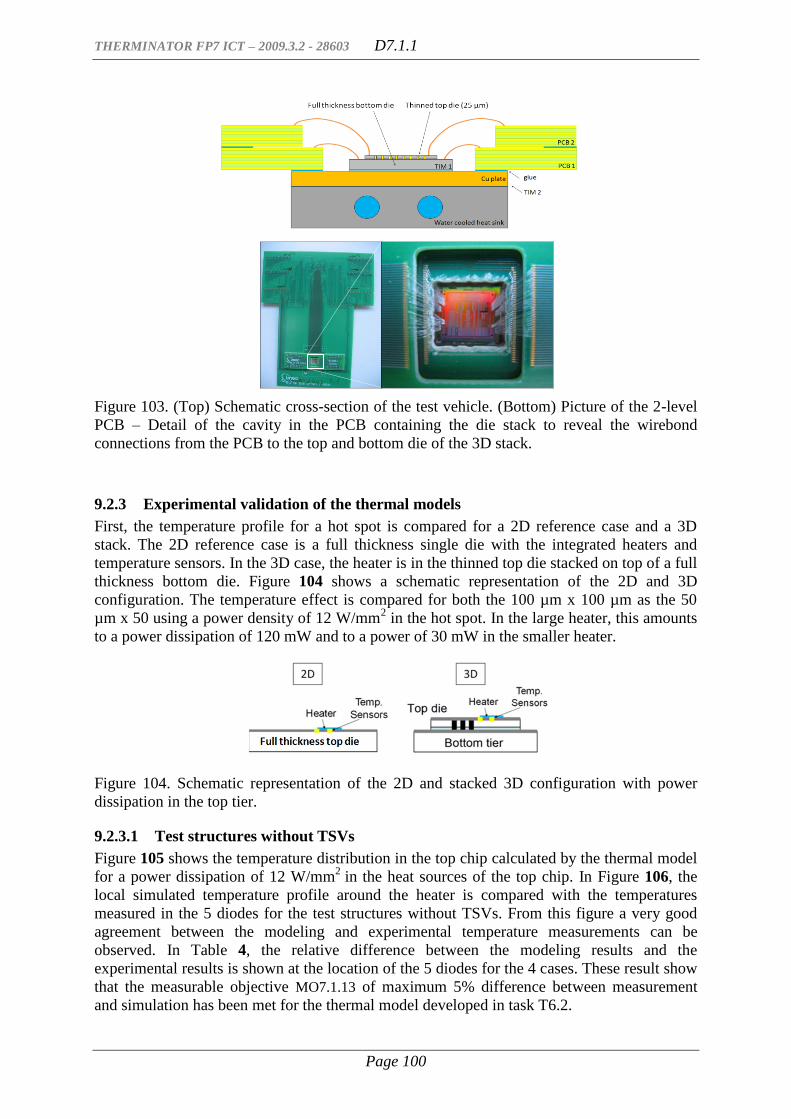
THERMINATOR FP7 ICT – 2009.3.2 - 28603 D7.1.1
Page 100
Figure 103. (Top) Schematic cross-section of the test vehicle. (Bottom) Picture of the 2-level
PCB – Detail of the cavity in the PCB containing the die stack to reveal the wirebond
connections from the PCB to the top and bottom die of the 3D stack.
9.2.3 Experimental validation of the thermal models
First, the temperature profile for a hot spot is compared for a 2D reference case and a 3D
stack. The 2D reference case is a full thickness single die with the integrated heaters and
temperature sensors. In the 3D case, the heater is in the thinned top die stacked on top of a full
thickness bottom die. Figure 104 shows a schematic representation of the 2D and 3D
configuration. The temperature effect is compared for both the 100 µm x 100 µm as the 50
µm x 50 using a power density of 12 W/mm2 in the hot spot. In the large heater, this amounts
to a power dissipation of 120 mW and to a power of 30 mW in the smaller heater.
Figure 104. Schematic representation of the 2D and stacked 3D configuration with power
dissipation in the top tier.
9.2.3.1 Test structures without TSVs
Figure 105 shows the temperature distribution in the top chip calculated by the thermal model
for a power dissipation of 12 W/mm2
in the heat sources of the top chip. In Figure 106, the
local simulated temperature profile around the heater is compared with the temperatures
measured in the 5 diodes for the test structures without TSVs. From this figure a very good
agreement between the modeling and experimental temperature measurements can be
observed. In Table 4, the relative difference between the modeling results and the
experimental results is shown at the location of the 5 diodes for the 4 cases. These result show
that the measurable objective MO7.1.13 of maximum 5% difference between measurement
and simulation has been met for the thermal model developed in task T6.2.

THERMINATOR FP7 ICT – 2009.3.2 - 28603 D7.1.1
Page 101
Figure 105. Simulation result from the thermal model from T6.2 for the temperature
distribution in the top chip of a two die stack for a power density of 12W/mm2 in all heat
sources shown in the layout in Figure 101.
Figure 106. Temperature profile simulation (solid lines) and experimental (markers and error
bars) results for a power dissipation of 12 W/mm2 in 100x100 µm
2 and 50x50 µm
2 heaters in
the 2D and 3D configuration for the test structures without TSVs.
Table 4. Relative difference between the modeling and experimental results at the diode
locations for the temperature profiles of Figure 106.
Case100x100
3D
100x100
2D
50x50
3D
50x50
2D
Diode 1 4.11% 5.14% 5.06% 4.97%
Diode 2 3.72% -3.41% 4.72% 4.29%
Diode 3 -4.73% -4.50% -2.93% -4.44%
Diode 4 -4.76% -3.50% -4.15% 4.12%
Diode 5 -6.32% -2.69% -4.65% -5.45%
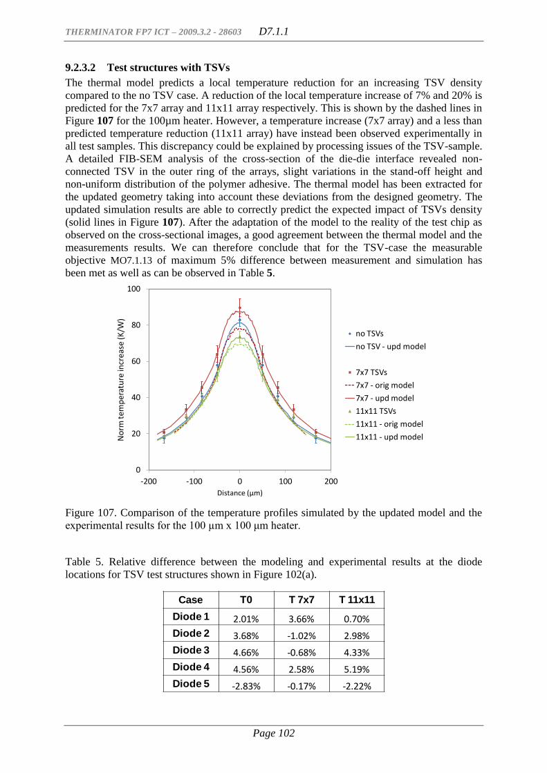
THERMINATOR FP7 ICT – 2009.3.2 - 28603 D7.1.1
Page 102
9.2.3.2 Test structures with TSVs
The thermal model predicts a local temperature reduction for an increasing TSV density
compared to the no TSV case. A reduction of the local temperature increase of 7% and 20% is
predicted for the 7x7 array and 11x11 array respectively. This is shown by the dashed lines in
Figure 107 for the 100µm heater. However, a temperature increase (7x7 array) and a less than
predicted temperature reduction (11x11 array) have instead been observed experimentally in
all test samples. This discrepancy could be explained by processing issues of the TSV-sample.
A detailed FIB-SEM analysis of the cross-section of the die-die interface revealed non-
connected TSV in the outer ring of the arrays, slight variations in the stand-off height and
non-uniform distribution of the polymer adhesive. The thermal model has been extracted for
the updated geometry taking into account these deviations from the designed geometry. The
updated simulation results are able to correctly predict the expected impact of TSVs density
(solid lines in Figure 107). After the adaptation of the model to the reality of the test chip as
observed on the cross-sectional images, a good agreement between the thermal model and the
measurements results. We can therefore conclude that for the TSV-case the measurable
objective MO7.1.13 of maximum 5% difference between measurement and simulation has
been met as well as can be observed in Table 5.
Figure 107. Comparison of the temperature profiles simulated by the updated model and the
experimental results for the 100 µm x 100 μm heater.
Table 5. Relative difference between the modeling and experimental results at the diode
locations for TSV test structures shown in Figure 102(a).
0
20
40
60
80
100
-200 -100 0 100 200
No
rm te
mp
erat
ure
incr
ease
(K/W
)
Distance (µm)
no TSVs
no TSV - upd model
7x7 TSVs
7x7 - orig model
7x7 - upd model
11x11 TSVs
11x11 - orig model
11x11 - upd model
Case T0 T 7x7 T 11x11
Diode 1 2.01% 3.66% 0.70%
Diode 2 3.68% -1.02% 2.98%
Diode 3 4.66% -0.68% 4.33%
Diode 4 4.56% 2.58% 5.19%
Diode 5 -2.83% -0.17% -2.22%
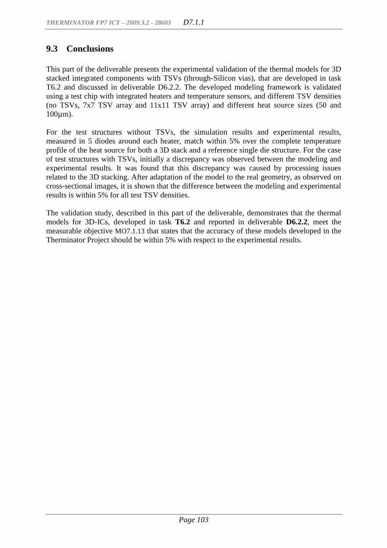
THERMINATOR FP7 ICT – 2009.3.2 - 28603 D7.1.1
Page 103
9.3 Conclusions
This part of the deliverable presents the experimental validation of the thermal models for 3D
stacked integrated components with TSVs (through-Silicon vias), that are developed in task
T6.2 and discussed in deliverable D6.2.2. The developed modeling framework is validated
using a test chip with integrated heaters and temperature sensors, and different TSV densities
(no TSVs, 7x7 TSV array and 11x11 TSV array) and different heat source sizes (50 and
100µm).
For the test structures without TSVs, the simulation results and experimental results,
measured in 5 diodes around each heater, match within 5% over the complete temperature
profile of the heat source for both a 3D stack and a reference single die structure. For the case
of test structures with TSVs, initially a discrepancy was observed between the modeling and
experimental results. It was found that this discrepancy was caused by processing issues
related to the 3D stacking. After adaptation of the model to the real geometry, as observed on
cross-sectional images, it is shown that the difference between the modeling and experimental
results is within 5% for all test TSV densities.
The validation study, described in this part of the deliverable, demonstrates that the thermal
models for 3D-ICs, developed in task T6.2 and reported in deliverable D6.2.2, meet the
measurable objective MO7.1.13 that states that the accuracy of these models developed in the
Therminator Project should be within 5% with respect to the experimental results.
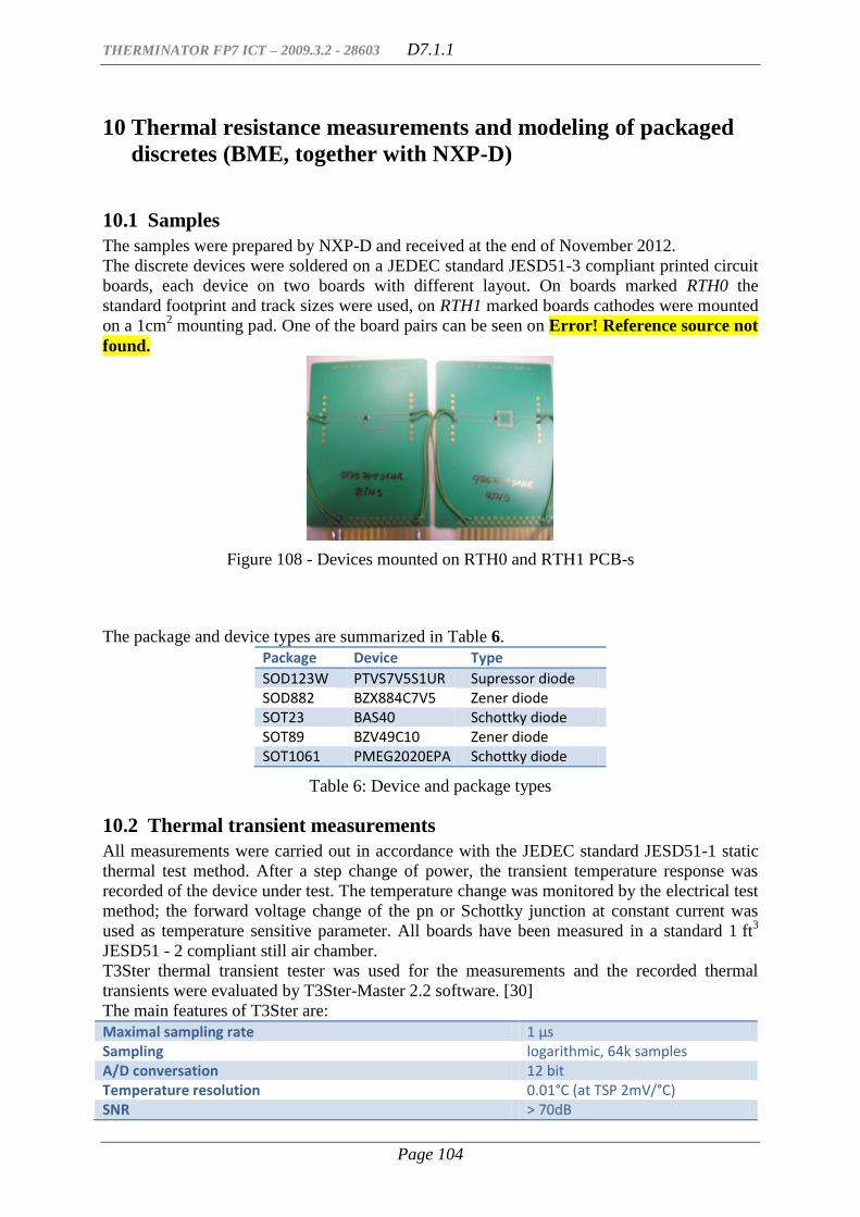
THERMINATOR FP7 ICT – 2009.3.2 - 28603 D7.1.1
Page 104
10 Thermal resistance measurements and modeling of packaged
discretes (BME, together with NXP-D)
10.1 Samples
The samples were prepared by NXP-D and received at the end of November 2012.
The discrete devices were soldered on a JEDEC standard JESD51-3 compliant printed circuit
boards, each device on two boards with different layout. On boards marked RTH0 the
standard footprint and track sizes were used, on RTH1 marked boards cathodes were mounted
on a 1cm2 mounting pad. One of the board pairs can be seen on Error! Reference source not
found.
Figure 108 - Devices mounted on RTH0 and RTH1 PCB-s
The package and device types are summarized in Table 6.
Package Device Type
SOD123W PTVS7V5S1UR Supressor diode SOD882 BZX884C7V5 Zener diode SOT23 BAS40 Schottky diode SOT89 BZV49C10 Zener diode SOT1061 PMEG2020EPA Schottky diode
Table 6: Device and package types
10.2 Thermal transient measurements
All measurements were carried out in accordance with the JEDEC standard JESD51-1 static
thermal test method. After a step change of power, the transient temperature response was
recorded of the device under test. The temperature change was monitored by the electrical test
method; the forward voltage change of the pn or Schottky junction at constant current was
used as temperature sensitive parameter. All boards have been measured in a standard 1 ft3
JESD51 - 2 compliant still air chamber.
T3Ster thermal transient tester was used for the measurements and the recorded thermal
transients were evaluated by T3Ster-Master 2.2 software. [30]
The main features of T3Ster are:
Maximal sampling rate 1 μs Sampling logarithmic, 64k samples A/D conversation 12 bit Temperature resolution 0.01°C (at TSP 2mV/°C) SNR > 70dB
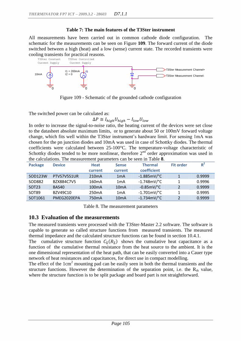
THERMINATOR FP7 ICT – 2009.3.2 - 28603 D7.1.1
Page 105
Table 7: The main features of the T3Ster instrument
All measurements have been carried out in common cathode diode configuration. The
schematic for the measurements can be seen on Figure 109. The forward current of the diode
switched between a high (heat) and a low (sense) current state. The recorded transients were
cooling transients for practical reasons.
Figure 109 - Schematic of the grounded cathode configuration
The switched power can be calculated as:
In order to increase the signal-to-noise ratio, the heating current of the devices were set close
to the datasheet absolute maximum limits, or to generate about 50 or 100mV forward voltage
change, which fits well within the T3Ster instrument’s hardware limit. For sensing 1mA was
chosen for the pn junction diodes and 10mA was used in case of Schottky diodes. The thermal
coefficients were calculated between 25-100°C. The temperature-voltage characteristic of
Schottky diodes tended to be more nonlinear, therefore 2nd
order approximation was used in
the calculations. The measurement parameters can be seen in Table 8.
Package Device Heat current
Sense current
Thermal coefficient
Fit order R2
SOD123W PTVS7V5S1UR 210mA 1mA -1.885mV/°C 1 0.9999 SOD882 BZX884C7V5 160mA 1mA -1.748mV/°C 1 0.9996 SOT23 BAS40 100mA 10mA -0.85mV/°C 2 0.9999 SOT89 BZV49C10 250mA 1mA -1.701mV/°C 1 0.9995 SOT1061 PMEG2020EPA 750mA 10mA -1.734mV/°C 2 0.9999
Table 8. The measurement parameters
10.3 Evaluation of the measurements
The measured transients were processed with the T3Ster-Master 2.2 software. The software is
capable to generate so called structure functions from measured transients. The measured
thermal impedance and the calculated structure functions can be found in section 10.4.1.
The cumulative structure function ( ) shows the cumulative heat capacitance as a
function of the cumulative thermal resistance from the heat source to the ambient. It is the
one dimensional representation of the heat path, that can be easily converted into a Cauer type
network of heat resistances and capacitances, for direct use in compact modelling.
The effect of the 1cm2 mounting pad can be easily seen in both the thermal transients and the
structure functions. However the determination of the separation point, i.e. the Rth value,
where the structure function is to be split package and board part is not straightforward.
10mA
0
T3Ster Measurement Channel-
T3Ster Measurement Channel+
T3Ster Controlled
Current Supply
0
I5I1 = 200mAI2 = 0
T3Ster Constant
Current Supply
0
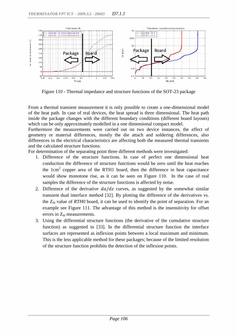
THERMINATOR FP7 ICT – 2009.3.2 - 28603 D7.1.1
Page 106
Figure 110 - Thermal impedance and structure functions of the SOT-23 package
From a thermal transient measurement it is only possible to create a one-dimensional model
of the heat path. In case of real devices, the heat spread is three dimensional. The heat path
inside the package changes with the different boundary conditions (different board layouts)
which can be only approximately modelled in a one dimensional compact model.
Furthermore the measurements were carried out on two device instances, the effect of
geometry or material differences, mostly the die attach and soldering differences, also
differences in the electrical characteristics are affecting both the measured thermal transients
and the calculated structure functions.
For determination of the separating point three different methods were investigated:
1. Difference of the structure functions. In case of perfect one dimensional heat
conduction the difference of structure functions would be zero until the heat reaches
the 1cm2 copper area of the RTH1 board, then the difference in heat capacitance
would show monotone rise, as it can be seen on Figure 110. In the case of real
samples the difference of the structure functions is affected by noise.
2. Difference of the derivative curves, as suggested by the somewhat similar
transient dual interface method [32]. By plotting the difference of the derivatives vs.
the Zth value of RTH0 board, it can be used to identify the point of separation. For an
example see Figure 111. The advantage of this method is the insensitivity for offset
errors in Zth measurements.
3. Using the differential structure functions (the derivative of the cumulative structure
function) as suggested in [33]. In the differential structure function the interface
surfaces are represented as inflexion points between a local maximum and minimum.
This is the less applicable method for these packages; because of the limited resolution
of the structure function prohibits the detection of the inflexion points.
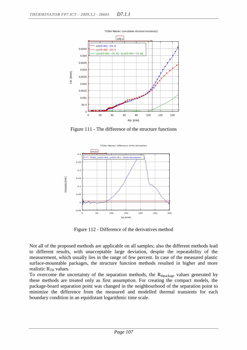
THERMINATOR FP7 ICT – 2009.3.2 - 28603 D7.1.1
Page 107
Figure 111 - The difference of the structure functions
Figure 112 - Difference of the derivatives method
Not all of the proposed methods are applicable on all samples; also the different methods lead
to different results, with unacceptable large deviation, despite the repeatability of the
measurement, which usually lies in the range of few percent. In case of the measured plastic
surface-mountable packages, the structure function methods resulted in higher and more
realistic RTH values.
To overcome the uncertainty of the separation methods, the Rthpackage values generated by
these methods are treated only as first assumption. For creating the compact models, the
package-board separation point was changed in the neighbourhood of the separation point to
minimize the difference from the measured and modelled thermal transients for each
boundary condition in an equidistant logarithmic time scale.
0 20 40 60 80 100 120 140
0
5e-4
0.001
0.0015
0.002
0.0025
0.003
0.0035
0.004
0.0045
Rth [K/W]
Cth
[W
s/K
]
T3Ster Master: cumulative structure function(s)
106.1
sot23-rth1 - Ch. 6
sot23-rth0 - Ch. 6
| [sot23-rth1 - Ch. 6] - [sot23-rth0 - Ch. 6]|
0 50 100 150 200 250 300
-0.05
0
0.05
0.1
0.15
0.2
0.25
0.3
Zja [K/W]
Del
ta(d
a/dz
) [K
/W/-]
T3Ster Master: Difference of the derivatives
Rth-JC = -363.02 K/W
84.02
TDIM_sot23-rth0_sot23-rth1 - Delta derivatives

THERMINATOR FP7 ICT – 2009.3.2 - 28603 D7.1.1
Page 108
10.4 Overview measurement results
10.4.1 The Zth(t) and the structure functions of the measured devices.
10.4.1.1 SOD123W
10.4.1.2 SOD882
1e-6 1e-5 1e-4 0.001 0.01 0.1 1 10 100 1000-50
0
50
100
150
200
250
300
Time [s]
No
rma
lize
d te
mp
era
ture
ris
e [°C
]
T3Ster Master: Zth
120
136
sod123w-rth0 - Ch. 6 From Measurement
sod123w-rth1 - Ch. 6 From Measurement
0 50 100 150 200 250 300
1e-4
0.01
1
100
10000
Rth [K/W]
Cth
[W
s/K
]
T3Ster Master: cumulative structure function(s)
136 120
sod123w-rth0 - Ch. 6
sod123w-rth1 - Ch. 6
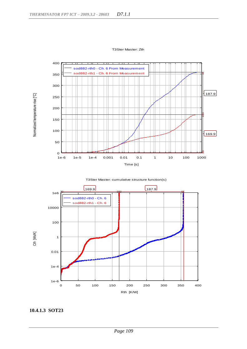
THERMINATOR FP7 ICT – 2009.3.2 - 28603 D7.1.1
Page 109
10.4.1.3 SOT23
1e-6 1e-5 1e-4 0.001 0.01 0.1 1 10 100 1000
0
50
100
150
200
250
300
350
400
Time [s]
Nor
mal
ized
tem
pera
ture
rise
[°C
]
T3Ster Master: Zth
187.9
169.9
sod882-rth0 - Ch. 6 From Measurement
sod882-rth1 - Ch. 6 From Measurement
0 50 100 150 200 250 300 350 400
1e-6
1e-4
0.01
1
100
10000
1e6
Rth [K/W]
Cth
[W
s/K
]
T3Ster Master: cumulative structure function(s)
169.9 187.9
sod882-rth0 - Ch. 6
sod882-rth1 - Ch. 6

THERMINATOR FP7 ICT – 2009.3.2 - 28603 D7.1.1
Page 110
1e-6 1e-5 1e-4 0.001 0.01 0.1 1 10 100 1000-50
0
50
100
150
200
250
300
350
400
450
Time [s]
No
rma
lize
d te
mp
era
ture
ris
e [°C
]T3Ster Master: Zth
102
299
sot23_rth1 - Ch. 6 From Measurement
sot23_rth0 - Ch. 6 From Measurement
0 50 100 150 200 250 300 350 400 4501e-6
1e-4
0.01
1
100
10000
1e6
Rth [K/W]
Cth
[W
s/K
]
T3Ster Master: cumulative structure function(s)
299 102
sot23_rth0 - Ch. 6
sot23_rth1 - Ch. 6
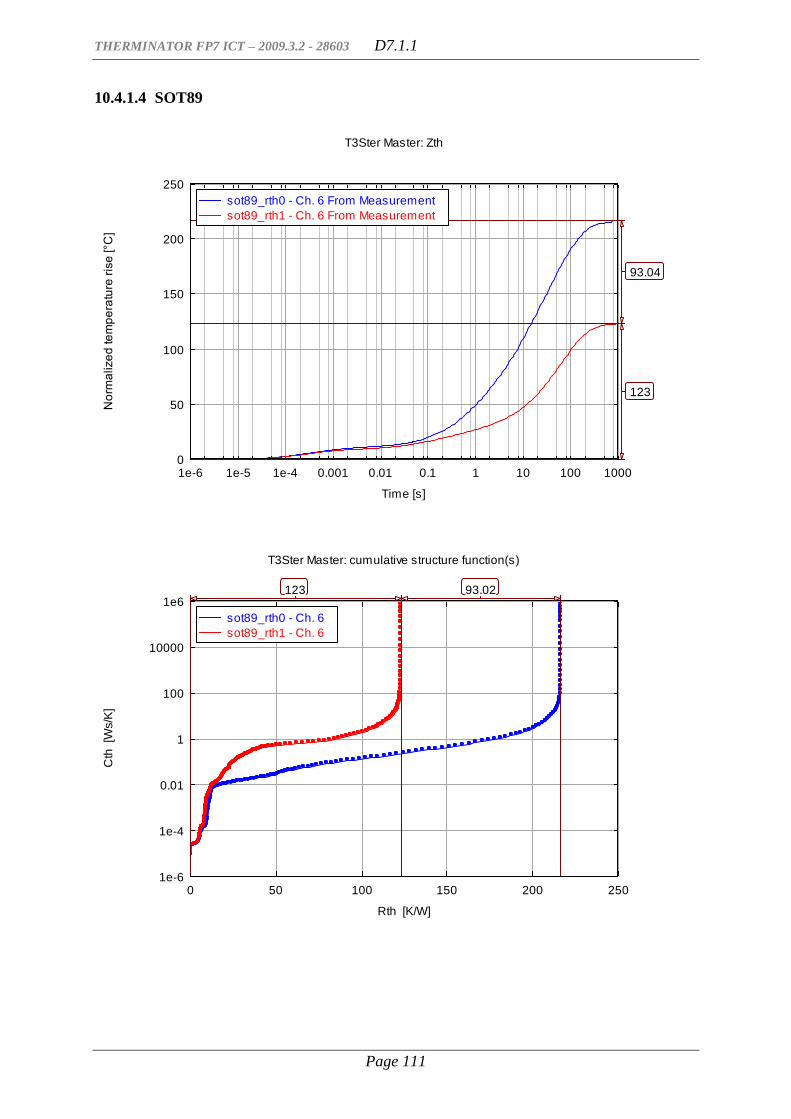
THERMINATOR FP7 ICT – 2009.3.2 - 28603 D7.1.1
Page 111
10.4.1.4 SOT89
1e-6 1e-5 1e-4 0.001 0.01 0.1 1 10 100 10000
50
100
150
200
250
Time [s]
No
rma
lize
d te
mp
era
ture
ris
e [°C
]
T3Ster Master: Zth
93.04
123
sot89_rth0 - Ch. 6 From Measurement
sot89_rth1 - Ch. 6 From Measurement
0 50 100 150 200 2501e-6
1e-4
0.01
1
100
10000
1e6
Rth [K/W]
Cth
[W
s/K
]
T3Ster Master: cumulative structure function(s)
123 93.02
sot89_rth0 - Ch. 6
sot89_rth1 - Ch. 6
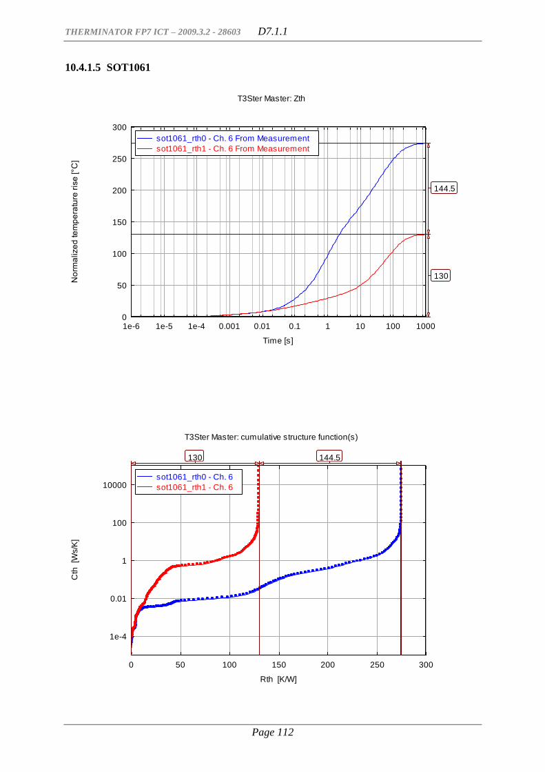
THERMINATOR FP7 ICT – 2009.3.2 - 28603 D7.1.1
Page 112
10.4.1.5 SOT1061
1e-6 1e-5 1e-4 0.001 0.01 0.1 1 10 100 10000
50
100
150
200
250
300
Time [s]
No
rma
lize
d te
mp
era
ture
ris
e [°C
]
T3Ster Master: Zth
144.5
130
sot1061_rth0 - Ch. 6 From Measurement
sot1061_rth1 - Ch. 6 From Measurement
0 50 100 150 200 250 300
1e-4
0.01
1
100
10000
Rth [K/W]
Cth
[W
s/K
]
T3Ster Master: cumulative structure function(s)
130 144.5
sot1061_rth0 - Ch. 6
sot1061_rth1 - Ch. 6
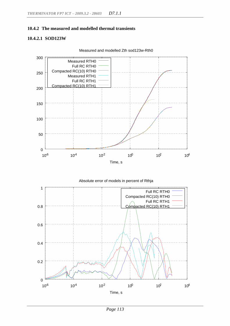
THERMINATOR FP7 ICT – 2009.3.2 - 28603 D7.1.1
Page 113
10.4.2 The measured and modelled thermal transients
10.4.2.1 SOD123W
0
50
100
150
200
250
300
10-6 10-4 10-2 100 102 104
Norm
aliz
ed tem
pera
ture
ris
e, C
Time, s
Measured and modelled Zth sod123w-Rth0
Measured RTH0
Full RC RTH0
Compacted RC(10) RTH0
Measured RTH1
Full RC RTH1
Compacted RC(10) RTH1
0
0.2
0.4
0.6
0.8
1
10-6 10-4 10-2 100 102 104
Err
or,
%
Time, s
Absolute error of models in percent of Rthja
Full RC RTH0
Compacted RC(10) RTH0
Full RC RTH1
Compacted RC(10) RTH1
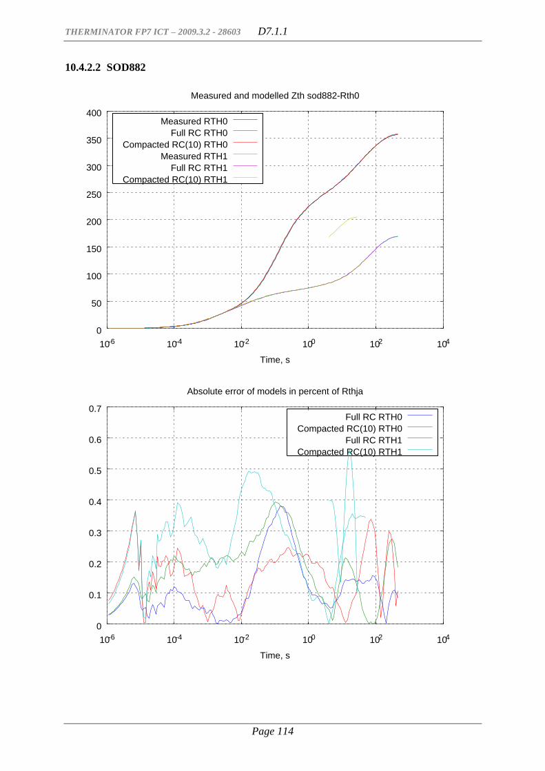
THERMINATOR FP7 ICT – 2009.3.2 - 28603 D7.1.1
Page 114
10.4.2.2 SOD882
0
50
100
150
200
250
300
350
400
10-6 10-4 10-2 100 102 104
Norm
aliz
ed tem
pera
ture
ris
e, C
Time, s
Measured and modelled Zth sod882-Rth0
Measured RTH0
Full RC RTH0
Compacted RC(10) RTH0
Measured RTH1
Full RC RTH1
Compacted RC(10) RTH1
0
0.1
0.2
0.3
0.4
0.5
0.6
0.7
10-6 10-4 10-2 100 102 104
Err
or,
%
Time, s
Absolute error of models in percent of Rthja
Full RC RTH0
Compacted RC(10) RTH0
Full RC RTH1
Compacted RC(10) RTH1

THERMINATOR FP7 ICT – 2009.3.2 - 28603 D7.1.1
Page 115
10.4.2.3 SOT23
0
100
200
300
400
500
10-6 10-4 10-2 100 102 104
Norm
aliz
ed tem
pera
ture
ris
e, C
Time, s
Measured and modelled Zth sot23-Rth0
Measured RTH0
Full RC RTH0
Compacted RC(10) RTH0
Measured RTH1
Full RC RTH1
Compacted RC(10) RTH1
0
0.2
0.4
0.6
0.8
1
1.2
1.4
10-6 10-4 10-2 100 102 104
Err
or,
%
Time, s
Absolute error of models in percent of Rthja
Full RC RTH0
Compacted RC(10) RTH0
Full RC RTH1
Compacted RC(10) RTH1

THERMINATOR FP7 ICT – 2009.3.2 - 28603 D7.1.1
Page 116
10.4.2.4 SOT89
0
50
100
150
200
250
10-6 10-4 10-2 100 102 104
Norm
aliz
ed tem
pera
ture
ris
e, C
Time, s
Measured and modelled Zth sot89-Rth0
Measured RTH0
Full RC RTH0
Compacted RC(10) RTH0
Measured RTH1
Full RC RTH1
Compacted RC(10) RTH1
0
0.2
0.4
0.6
0.8
1
10-6 10-4 10-2 100 102 104
Err
or,
%
Time, s
Absolute error of models in percent of Rthja
Full RC RTH0
Compacted RC(10) RTH0
Full RC RTH1
Compacted RC(10) RTH1
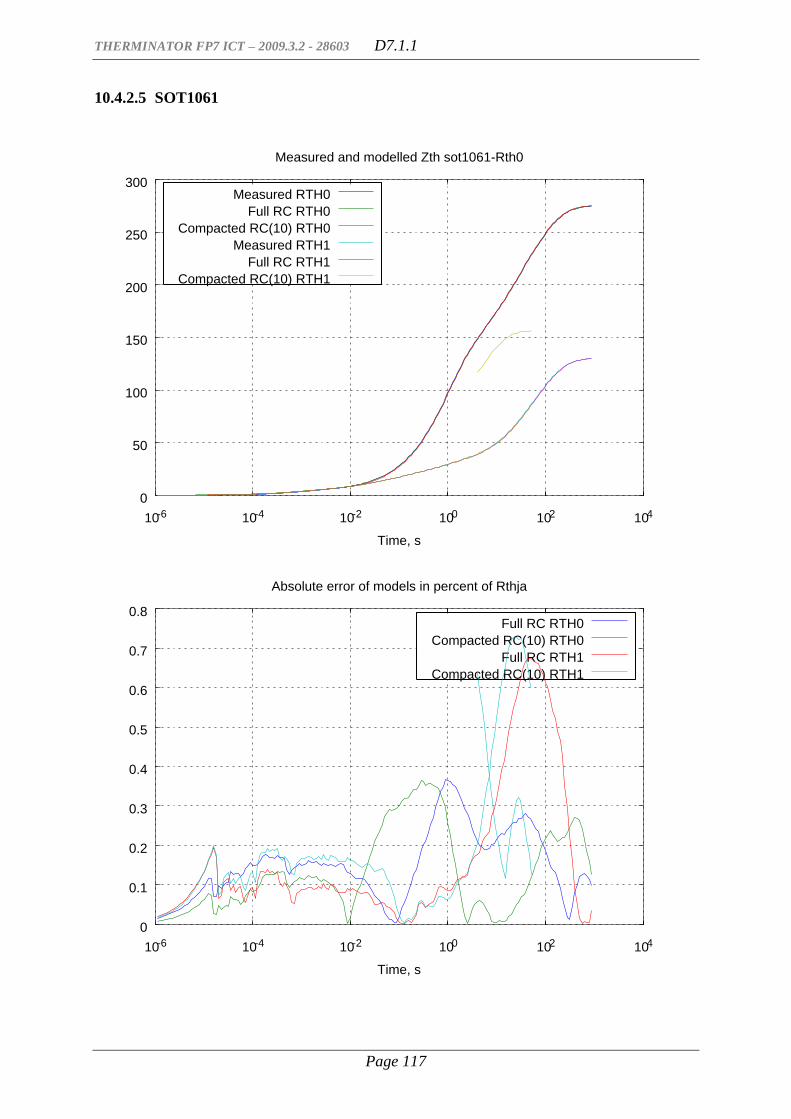
THERMINATOR FP7 ICT – 2009.3.2 - 28603 D7.1.1
Page 117
10.4.2.5 SOT1061
0
50
100
150
200
250
300
10-6 10-4 10-2 100 102 104
Norm
aliz
ed tem
pera
ture
ris
e, C
Time, s
Measured and modelled Zth sot1061-Rth0
Measured RTH0
Full RC RTH0
Compacted RC(10) RTH0
Measured RTH1
Full RC RTH1
Compacted RC(10) RTH1
0
0.1
0.2
0.3
0.4
0.5
0.6
0.7
0.8
10-6 10-4 10-2 100 102 104
Err
or,
%
Time, s
Absolute error of models in percent of Rthja
Full RC RTH0
Compacted RC(10) RTH0
Full RC RTH1
Compacted RC(10) RTH1

THERMINATOR FP7 ICT – 2009.3.2 - 28603 D7.1.1
Page 118
10.5 Conclusions
The static thermal resistance of the different packages and boards can be seen in Table 9.
Package RTHJA Board- RTH0 RTHJA Board-RTH1 RTHJP
SOD123W 256 K/W 136 K/W 11 K/W SOD882 358 K/W 170 K/W 38.2 K/W SOT23 401 K/W 200 K/W 105 K/W SOT89 216 K/W 123 K/W 13.8 K/W SOT1061 274.5 K/W 130 K/W 7.9 K/W
Table 9: The static thermal resistances of the different packages and boards
From the separated package/board structure functions equivalent Cauer type models were
generated. The package models have about 29-51, the board models have 94-115 RC stages.
In order to increase the usability of these behaviour models in other simulators, the RC
ladders have been further compacted to contain ten RC elements for the package and the
boards.
Board- RTH0 Board-RTH1
full compact full compact Error (%) mean max mean max mean max mean max SOD123W 0.15 0.45 0.19 0.84 0.18 0.45 0.21 0.51 SOD882 0.11 0.38 0.18 0.39 0.15 0.37 0.26 0.53 SOT23 0.32 0.58 0.56 0.99 0.23 0.51 0.42 1.01 SOT89 0.15 0.47 0.26 0.63 0.32 0.75 0.37 0.90 SOT1061 0.15 0.37 0.13 0.36 0.16 0.67 0.18 0.73
Table 10: The average and the maximum of the error of compact models respect to the RTHJA
The error between measured and modelled Zth is defined as:
| |
The average value is calculated on an equidistant logarithmic scale from 1μs- to the length of
the thermal transient measurement.
Both maximal and average errors are in less or equal to 1 percent of the measured transients.
Using the compact model does not introduce significant errors.

THERMINATOR FP7 ICT – 2009.3.2 - 28603 D7.1.1
Page 119
11 Conclusions
In this deliverable, the validation of models and tools addressing the thermal behaviour of
electronic devices in many different technologies of relevance for the European semi-
conductor industry has been demonstrated. The models and tools have been developed in
WP2, 3, 4, 5, and 6 on advanced and new devices, technologies, and materials. The validation
was carried out on the test cases of WP1 and other examples provided by individual partners.
The validation activities concentrated on validation of TCAD tools and verification of
compact models, since the validation in T7.1 focussed on devices and elementary building
blocks. In this final conclusion, the major results are summarized, while a more detailed
overview of the results on each subject can be found in the conclusions section of each
chapter. The results in terms of measurable objectives and contributions to conferences and
journals are given in chapters 12 and 13, respectively.
In the validation activities, there has been a close cooperation between TCAD vendors,
universities, research institutes, and the European semiconductor industry. These
collaborations in Therminator have been very effective in terms of exchanging concepts and
ideas between partners, creating a valuable innovation infrastructure between universities,
research institutes, and the industry. Results of these collaborations include verified TCAD
for power devices (SNPS-CH, ST), devices in contactless identification ICs (SNPS-CH, FHG,
NXP-D), and advanced CMOS (SNPS-CH, IMC). Moreover, the cooperation between BME
and NXP-D has resulted in compact thermal models for packaged discretes validated against
measurements. Furthermore, there have been several activities to study and improve the
understanding of electronic devices of the (near) future, resulting in accurate models for 3D
ICs (IMEC), compact models for GaN-HEMTs (NXP-NL), and a capacitance-based thermal
characterization technique for low-power devices (UNIBO). Finally, the industrial partners
have shown the usefulness of the tools developed in Therminator by demonstrating their
integration into design flows. Examples include the integration of PSP models for advanced
CMOS devices into the IMC design flow, the RF-LDMOS electro-thermal models into the
NXP design tools, and the thermal-aware design framework of ST for high-voltage transistors
in automotive applications. The integration of the developed tools into the (existing) design
flows of the industrial partners is an important step in the commercial exploitability of the
Therminator project, resulting in an advantageous position of the partners with respect to the
competition.

THERMINATOR FP7 ICT – 2009.3.2 - 28603 D7.1.1
Page 120
12 Measurable objectives
The Therminator project objectives are
1. New modeling and simulation capabilities to support accurate circuit thermal analysis
and simulation
2. Innovative thermal-aware design techniques, methodologies and prototype tools for
controlling, compensating and managing thermally-induced effects on parameters
such as timing, (dynamic and leakage) power, reliability and yield
3. Demonstration of the accuracy and ease of integration within existing design flows of
the new models by validation against measured data obtained on ad-hoc silicon
structures
4. Demonstration of the applicability and effectiveness of the new design solutions
through manufacturing of test-chips featuring leading-edge silicon technology, as
available from some of the project partners
5. Demonstration of the usability and effectiveness of the new design methodologies and
tools by their application to industry-strength design cases made available by some of
the project partners
In order to quantify the output of the validation work presented in this deliverable, measurable
objectives have been defined. In the table below, all the measurable objectives of T7.1 are
summarized. In this table, it is also shown to which test case of WP1, and to which
Therminator’s project objectives the measurable objectives are related. Since T7.1 focuses on
validation and verification of models and tools of devices and elementary building block, the
majority of the measurable objectives are related to Therminator’s project objective 1. In T7.2
and T7.3, the measurable objectives will be more connected to the other Therminator’s
project objectives (2-5).
Area Measurable
objective
Innovation Metric Quantification Test case Project
objective
7.1
Validation
of models
on test
structures
MO7.1.1 Thermal resistance
measurements on
power
devices
Validation thermal models
RF-LDMOS and GaN-
HEMT
(yes/no) [NXP-NL]
Test
structures:
Testcase 2
1
MO7.1.2 Reuse by adapting
electro-thermal
modeling developed
on RF power
technologies for other
types of devices
Reuse and adapt electro-
thermal model GaN-HEMT
for GaN Schottky diodes.
Reuse and adapt electro-
thermal model RF-LDMOS
for SOI-LDMOS
Error within 15% [NXP-
NL]
Test case 2 3
MO7.1.3 Integration and
demonstration of
tools on industry-
strength designs
Integration of the electro-
thermal model for RF-
LDMOS , developed within
Therminator, into design
tools and validation on
large signal application
data.(yes/no) [NXP-NL]
Test case 2 5
MO7.1.4 WP5: Validate
thermal
Error between
measurements and
Testcase 2 1

THERMINATOR FP7 ICT – 2009.3.2 - 28603 D7.1.1
Page 121
models of discrete
power
devices developed in
WP5
(not existing before
Therminator) with
measurements
simulation within 10%.
[ST,SNPS-CH]
MO7.1.5 Validate 3D TCAD
model
for 28nm/32nm
CMOS
developed in WP2
Error between
measurements and
simulation within 20%.
[SNPS-CH]
Testcase 3 1
MO7.1.6 Validate the high-k
metal
gate 28nm CMOS
models
developed in WP2,
with
cross-technology
reference
to 40 nm
Error between
measurements and
simulation within 20 %
[IMC]
Testcase 3 1
MO7.1.7 Innovative thermal-
aware design
techniques,
methodologies and
prototype tools for
controlling,
compensating and
managing thermally-
induced effects on
parameters such as
timing, (dynamic and
leakage) power,
reliability and yield
Determine the temperature
inversion intersection point
of two temperatures
corresponding supply
voltage within 20% for
relevant parameters as
performance and Ion.
[IMC]
Test case 3 2
MO7.1.8 Validate the
high-k metal
gate 28nm
CMOS models
developed in
WP2, with cross-
technology
reference to 40
nm
Testcase 3 1
Error between
measurements and
simulation within 20 % .
[IMC]
Test case 3 3
MO7.1.9 Demonstration of the
applicability and
effectiveness of the
new design solutions
through
manufacturing of
test-chips featuring
leading-edge silicon
technology, as
available from some
of the project partners
Demonstration of model
hardware correlation based
on 40nm and 28nm
testchips (one or more
testchips per technology).
[IMC]
Test case 3 4
MO7.1.10 Demonstration of the The circuit-referenced PSP- Test case 3 5
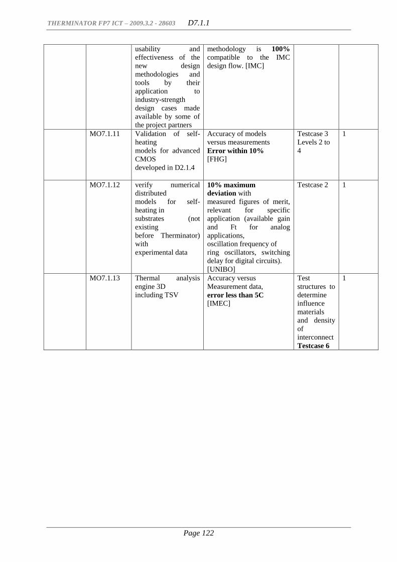
THERMINATOR FP7 ICT – 2009.3.2 - 28603 D7.1.1
Page 122
usability and
effectiveness of the
new design
methodologies and
tools by their
application to
industry-strength
design cases made
available by some of
the project partners
methodology is 100%
compatible to the IMC
design flow. [IMC]
MO7.1.11 Validation of self-
heating
models for advanced
CMOS
developed in D2.1.4
Accuracy of models
versus measurements
Error within 10%
[FHG]
Testcase 3
Levels 2 to
4
1
MO7.1.12 verify numerical
distributed
models for self-
heating in
substrates (not
existing
before Therminator)
with
experimental data
10% maximum
deviation with
measured figures of merit,
relevant for specific
application (available gain
and Ft for analog
applications,
oscillation frequency of
ring oscillators, switching
delay for digital circuits).
[UNIBO]
Testcase 2 1
MO7.1.13 Thermal analysis
engine 3D
including TSV
Accuracy versus
Measurement data,
error less than 5C
[IMEC]
Test
structures to
determine
influence
materials
and density
of
interconnect
Testcase 6
1

THERMINATOR FP7 ICT – 2009.3.2 - 28603 D7.1.1
Page 123
13 Publications and presentations
A. Burenkov, J. Lorenz, “Self-heating effects in nano-scaled MOSFETs and thermal aware
compact models”, THERMINIC, 17th International Workshop on Thermal investigations of
ICs and Systems, Paris, 27-29 Sept. 2011, EDA Publishing, pp. 17-18.
FHG, “Tutorial on TCAD Simulations of Nano-CMOS Including Self-Heating” was held at
IMC in September 2011 at IMEC in March 2012
F. Beneventi, A. Bartolini, L. Benini, “Static Thermal Model Learning for High-Performance
Multicore Servers”, Computer Communications and Networks (ICCCN), 2011 Proceedings of
20th International Conference on, Issue Date: July 31 2011-Aug. 4 2011, On page(s): 1 – 6,
Location: Lahaina, HI, USA, ISSN: 1095-2055 Print ISBN: 978-1-4577-0637-0, 2011 IEEE
A. Bartolini, M. Cacciari, A. Tilli, L. Benini, “A distributed and self-calibrating model-
predictive controller for energy and thermal management of high-performance multicores”,
Design, Automation & Test in Europe Conference & Exhibition (DATE), 2011, Grenoble,
France 14-18 March 2011, On page(s): 1 – 6, ISSN : 1530-1591, Print ISBN: 978-1-61284-
208-0. IEEE Press 2011
A. Bartolini, M. Sadri, F. Beneventi, M. Cacciari, A. Tilli, L. Benini, “SCC Thermal Sensor
Characterization and Calibration”, 3rd Many-core Applications Research Community
(MARC) Symposium, Ettlingen, Germany, Issue Date : 5-6 June 2011, On page(s): 7-12, KIT
Scientific Publishing 2011, ISBN 978-3-86644-717-2
A. Bartolini, M. Sadri, F. Beneventi, M. Cacciari, A. Tilli, L. Benini, “A System Level
Approach to Multi-core Thermal Sensors Calibration”, Integrated Circuit and System Design.
Power and Timing Modeling, Optimization, and Simulation, Editor: Ayala J., García-Cámara
B., Prieto M., Ruggiero M., Sicard G., Book Series Title: Lecture Notes in Computer Science,
Page(s): 22- 31, Volume: 6951, Copyright: 2011, Publisher: Springer Berlin / Heidelberg,
ISBN: 978-3-642-24153-6
M. Sadri, A. Bartolini, L. Benini, “Single-Chip Cloud Computer thermal model”, Thermal
Investigations of ICs and Systems (THERMINIC), 2011 17th International Workshop on,
Paris, France 27-29 Sept. 2011, On page(s): 1 – 6, Print ISBN: 978-1-4577-0778-0, IEEE
Press 2011
A. Sassone, A. Calimera, A. Macii, E. Macii, M. Poncino, R. Goldman, V. Melikyan, E.
Babayan, S. Rinaudo, “Investigating the Effects of Inverted Temperature Dependence (ITD)
on Clock Distribution Networks”, Proceedings of Design, Automation & Test in Europe
(DATE’12) conference, Dresden, Germany, 2012.-P.165-167
Wei Liu, V. Tenace, A. Calimera, A. Macii, E. Macii, M. Poncino, “NBTI Effects on Tree-
Like Clock Distribution Networks”, GLSVLSI-12: accepted for publication
A. Sassone, W. Liu, A. Calimera, A. Macii, E. Macii, M. Poncino, “Modeling of thermally
induced skew variations in clock distribution network”, THERMINIC-11: IEEE Thermal
Investigations of ICs and Systems, 2011.
THERMINATOR FP7 ICT – 2009.3.2 - 28603 D7.1.1
Page 124
L. M. de Lima Silva, A. Calimera, A. Macii, E. Macii, M. Poncino, "Power Efficient
Variability Compensation Through Clustered Tunable Power-Gating", IEEE Journal on
Emerging and Selected Topics in Circuits and Systems, vol.1, no.3, Sept. 2011
M. Caldera, A. Calimera, A. Macii, E. Macii, M. Poncino , “Minimizing temperature
sensitivity of dual-Vt CMOS circuits using Simulated-Annealing on ISING-like models”,
THERMINIC-10: IEEE Thermal Investigations of ICs and Systems, 2010.
A. Calimera, A. Macii, E. Macii, S. Rinaudo, M. Poncino, “THERMINATOR: Modeling,
control and management of thermal effects in electronic circuits of the future”, THERMINIC-
10: IEEE Thermal Investigations of ICs and Systems, 2010.
A. Calimera,R. Bahar, E. Macii, M. Poncino, “Temperature-Insensitive Dual-Vth Synthesis
for Nanometer CMOS Technologies Under Inverse Temperature Dependence”, IEEE
Transactions on Very Large Scale Integration (VLSI) Systems, vol. 18, no. 11, 2010
A. Timár, M. Rencz, “Studying the influence of chip temperatures on timing integrity”, 12th
IEEE Latin-American Test Workshop. Brazil, 27-30. 03. 2011.
A Timár, M. Rencz, “Studying the Influence of Chip Temperatures on Timing Integrity Using
Improved Power Modeling”, JOURNAL OF LOW POWER ELECTRONICS 7: pp. 1-10.
(2011)
A Timár, Gy. Bognár, M. Rencz, “Improved power modeling in logi-thermal simulation”,
17th International Workshop on Thermal investigations of ICs and Systems. Paris, Paris,
France, 27-29. 09. 2011.
Gergely Nagy, András Poppe, “A Novel Simulation Environment Enabling Multilevel Power
Estimation of Digital Systems”, Proceedings of the 17th International Workshop on THERMal
INvestigation of ICs and Systems
G. Gangemi, “FP7-Funding Projects THERMINATOR, SMAC, MANON Overview”, MUGM
MunEDA User Group Meeting 2012, October 2012, Munich, Germany
Z. Abbas, M. Olivieri, A. Ripp, G. Strube, M. Yakupov, “Yield optimization for low power
current controlled current conveyor”, SBCCI 2012, September 2012, Brasília, Brazil
Colaci, G. Boarin, A. Roggero, L. Civardi, C. Roma, A. Ripp, M. Pronath, G. Strube:
“Systematic Analysis & Optimization of Analog/Mixed-Signal Circuits Balancing Accuracy
and Design Time”, SBCCI 2011 Brazil, September 2011, Sao Paolo, Brazil
N. Seller, “Optimization of a 2.133GHz level shifter in 28nm”, MUGM MunEDA User Group
Meeting 2011, Munich, Germany
U. Trautner, M. Pronath, “Synopsys Custom and Analog Mixed-Signal Overview & MunEDA
WiCkeD Integration”, MUGM MunEDA User Group Meeting 2010, Munich, Germany
S. Coparale, R. Rvatti, G. Setti, "Representation of PWM signals through time warping",
Acoustics, Speech and Signal Processing (ICASSP), 2012 IEEE International Conference on ,
vol., no., pp.3589-3592, 25-30 March 2012.

THERMINATOR FP7 ICT – 2009.3.2 - 28603 D7.1.1
Page 125
Reef Eilers, Malte Metzdorf, Sven Rosinger, Domenik Helms, Wolfgang Nebel, “Phase space
based NBTI model”, Proc. of International Workshop on Power and Timing Modeling,
Optimization and Simulation (PATMOS), 2012
Sven Rosinger, Malte Metzdorf, Domenik Helms, Wolfgang Nebel, “Behavioral-Level
Thermal- and Aging-Estimation Flow”, Proc. Of 12th Latin-American Test Workshop (LATW),
p. 1-6, 2011
V. Melikyan, A. Gevorgyan, A. Baghdasaryan, H. Melikyan, “Thermal Via’s Placement
Zones Identifying Using Voronoi Diagrams”, Proceedings of the 32th International Scientific
Conference Electronics and Nanotechnology (ELNANO 2012), Kiev, Ukraine, 2012.-P.77-79
V. Melikyan, Babayan E., Harutyunyan A., Melikyan N., Zargaryan G., “Method of
Reducing Thermal Dependence of Timing Delays of Digital Integrated Circuits”, Proceedings
of 5th All-Russian scientific-technical conference “Problems of Developing Advanced Micro-
and Nanoelectronic Systems -2012” (MES-2012), Moscow, Russia, 2012. –P409-412
V.Sh. Melikyan, A.A. Durgaryan, A.H. Balabanyan, E.H. Babayan, M. Stanojlovic, A.G.
Harutyunyan, “Process-voltage-temperature Variation Detection and Cancellation Using On-
Chip Phase-Locked Loop”, Proceedings of the 56th Electronics, Telecommunications,
Computers, Automatic Control and Nuclear Engineering (ETRAN) Conference, Zlatibor,
Serbia, 2012.-P.EL1.2-1-4
P. Bibilo, A. Solovev, V. Melikyan, A. Harutyunyan, E. Babayan, “Estimation of Power
Consumption of Digital CMOS Circuits Based on Logic Simulation of their Structural
Descriptions”, Proceedings of Engineering Academy of Armenia, Yerevan, Armenia, 2012. –
P.600-610
V. Melikyan, E. Babayan, A. Harutyunyan, “Pattern-Based Approach to Current Density
Verification”, Proceedings of the 4th Small Systems Simulation Symposium 2012, Nis,
Serbia, 2012.-P.58-61
V. Melikyan, A. Balabanyan, E. Babayan, A. Durgaryan, “Decreasing of Frequency
Variation in High-Speed Ring Oscillator using Bandgap Reference”, Proceedings of the 32th
International Scientific Conference Electronics and Nanotechnology (ELNANO 2012), Kiev,
Ukraine, 2012.-P.79-81
R. Roldman, K. Bartleson, T. Wood, V. Melikyan, E. Babayan, “Synopsys’ Low Power
Design Educational Platform”, Proceedings of the 9th European Workshop on
Microelectronics Education (EWME 2012), Grenoble, France, 2012.-P.23-26
V. Melikyan, E. Babayan, A. Harutyunyan, “Pattern-Based Approach to Current Density
Verification”,/ Electronics, Faculty of Electrical Engineering, University of Banja Luka,
Volume 16, Number 1, Serbia, 2012.-P.77-82
V. Melikyan, A. Harutyunyan, “Modeling of IC Interconnects and Power Rails”, Chartarapet,
Yerevan, 2012 (in Armenian)
V. Melikyan, A. Durgaryan, A. Khachatryan, H. Manukyan, E. Musayelyan, “Self-
compensating Low Noise Low Power PLL Design”, Proceedings of IEEE East-West Design &
Test Symposium (EWDTS’12), Kharkov, Ukraine, 2012.-P.29-33
THERMINATOR FP7 ICT – 2009.3.2 - 28603 D7.1.1
Page 126
V.Sh. Melikyan, S.V. Gavrilov, V.K. Aharonyan, N.K. Aslanyan, A.S. Hovhannisyan, “On-
die CMOS Termination Resistor for USB Transmitter”, RAs National Academy of Science
and SEUA, Yerevan, RA, Vol. 65, N 3, Yerevan, 2012.-P. 295-304
P. Magnone, C. Fiegna, G. Greco, G. Bazzano, E. Sangiorgi, S. Rinaudo, “Modeling of
Thermal Network in Silicon Power MOSFETs”, Ultimate Integration on Silicon (ULIS), 14-16
Marzo 2011, Cork, Ireland.
P. Magnone, C, Fiegna, G. Greco, G. Bazzano, S. Rinaudo, E. Sangiorgi, “Numerical
Simulation and Modeling of Thermal Transient in Silicon Power Devices”, Ultimate
Integration on Silicon (ULIS), pp. 153-156, 6-7 March 2012,. Grenoble (France).
P. Magnone, C, Fiegna, G. Greco, G. Bazzano, S. Rinaudo, E. Sangiorgi, “Numerical
Simulation and Modeling of Thermal Transient in Silicon Power Devices”, ELSEVIER Solid-
State Electronics, in press.
H. Oprins, V. Cherman, B. Vandevelde, M. Stucchi, G. Van der Plas, P. Marchal, and E.
Beyne, “Steady state and transient thermal analysis of hot spots in 3D stacked ICs using
dedicated test chips”, 27th Annual IEEE Thermal Measurement, Modeling and Management
Symposium (SEMI-Therm), March 20-24, 2011, 131-137.
H. Oprins, V. Cherman, B. Vandevelde, C. Torregiani, M. Stucchi, G. Van der Plas, P.
Marchal, and E. Beyne, “Characterization of the Thermal Impact of Cu-Cu bonds achieved
using TSVs on hot spot dissipation in 3D stacked ICs”, Proceedings of ECTC, May 30- June 1,
2011, 861-868.
H. Oprins, V. Cherman, “Numerical and experimental characterization of hot spot dissipation
in 3D stacks”, Electronics Cooling Magazine, Vol. 18(2), 2012, pp. 18-23.
D. Milosevic, H. Oprins, J. Ryckaert, P. Marchal, G. Van der Plas, “DRAM-on-logic Stack –
Calibrated Thermal and Mechanical Models Integrated into A Design Flow”, IEEE Custom
Integrated Circuits Conference (CICC), September 18-21 2011, San Jose, California, invited.
H .Oprins, V. Cherman, B. Vandevelde, G. Van der Plas, P. Marchal, and E. Beyne,
“Numerical and experimental characterization of the thermal behavior of a packaged DRAM-
on-logic stack”, 62nd
Electronic Components and Technology Conference - ECTC, 2012, pp.
1081-1088.
Gergely Nagy, László Pohl, András Timár, András Poppe, “Yield enhancement by logi-
thermal simulation based testing”, Proceedings of the 18th International Workshop on
THERMal INvestigation of ICs and Systems (THERMINIC'12). Budapest, Hungary,
2012.09.25-2012.09.27. pp. 196-199. Paper 42.
Gergely Nagy, András Timár, Albin Szalai, Márta Rencz, András Poppe, “New simulation
approaches supporting temperature-aware design of digital ICs”, Proceedings of the 28th
IEEE Semiconductor Thermal Measurement and Management Symposium (SEMI-
THERM'12). San Jose, USA, 2012.03.18-2012.03.22. pp. 313-318.(ISBN: 978-1-4673-1109-
0)
A Timar, M. Rencz, “Temperature dependent timing in standard cell designs”, Proceedings of
the 18th International Workshop on THERMal INvestigation. Budapest, Hungary,
2012.09.25-2012.09.27. pp. 179-183.
A Timar, M. Rencz, “Real-time heating and power characterization of cells in standard cell
designs”, MICROELECTRONICS JOURNAL (2012)IF: [0.919*]
THERMINATOR FP7 ICT – 2009.3.2 - 28603 D7.1.1
Page 127
A Timar, M. Rencz, “Acquiring real-time heating of cells in standard cell designs”,
Proceedings of the 13th IEEE Latin-American Test Workshop (LATW'12). Quito, Ecuador,
2012.04.10-2012.04.13. pp. 121-125.
Gergely Nagy, András Poppe, “Simulation Framework for Multilevel Power Estimation and
Timing Analysis of Digital Systems Allowing the Consideration of Thermal Effects”,
Proceedings of the 13th IEEE Latin-American Test Workshop (LATW'12). Quito, Ecuador,
2012.04.10-2012.04.13. pp. 1-5.