vhdl and verilog module1 - worcester polytechnic …users.wpi.edu/~rjduck/vhdl and verilog...
TRANSCRIPT

Jim Duckworth, WPI ECE 574 - Module 11
VHDL and Verilog – Module 1
Introduction
Jim Duckworth
ECE Department, WPI

Jim Duckworth, WPI ECE 574 - Module 12
Topics
• Background to VHDL
• Introduction to language
• Programmable Logic Devices
– CPLDs and FPGAs
– FPGA architecture
– Spartan 3 Starter Board and Nexys 2 Board
• Using VHDL to synthesize and implement a design
• Verilog overview

Jim Duckworth, WPI ECE 574 - Module 13
Hardware Description Languages
• Example HDL's : ABEL, VERILOG, VHDL
• Advantages:
– Documentation
– Flexibility (easier to make design changes or mods)
– Portability (if HDL is standard)
– One language for modeling, simulation (test benches), and
synthesis
– Let synthesis worry about gate generation
• Engineer productivity
• However: A different way of approaching design
– engineers are used to thinking and designing using graphics
(schematics) instead of text.
Jim Duckworth, WPI ECE 574 - Module 14
VHDL
• VHSIC Hardware Description Language– Very High Speed Integrated Circuit
• Standard language used to describe digital hardware devices, systems and components– Developed initially for documentation
• VHDL program was an offshoot of the US Government's VHSIC Program
• Approved as an IEEE Standard in December 1987 (IEEE standard 1076-1987)– Revised - now 1076-1993 (supported by all tools)
– Work under way on VHDL-200X
• Integration of 1164 std
• General improvements, etc
Jim Duckworth, WPI ECE 574 - Module 15
VHDL References
• IEEE Standard VHDL Language Reference Manual (1076
– 1993) (1076-2002)
• “RTL Hardware Design using VHDL – Coding for
Efficiency, Portability, and Scalability” by Pong P. Chu,
Wiley-InterScience, 2006
• “Introductory VHDL From Simulation to Synthesis by
Sudhakar Yalamanchilli, 2002, Xilinx Design Series,
Prentice Hall
• “VHDL Made Easy” by David Pellerin and Douglas
Taylor, 1997, Prentice Hall
Jim Duckworth, WPI ECE 574 - Module 16
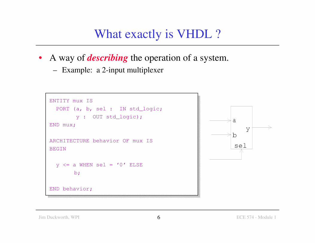
What exactly is VHDL ?
• A way of describing the operation of a system.
– Example: a 2-input multiplexer
ENTITY mux IS
PORT (a, b, sel : IN std_logic;
y : OUT std_logic);
END mux;
ARCHITECTURE behavior OF mux IS
BEGIN
y <= a WHEN sel = ‘0’ ELSE
b;
END behavior;
Jim Duckworth, WPI ECE 574 - Module 17
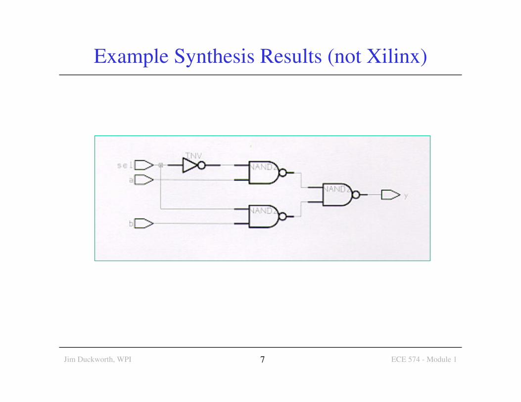
Example Synthesis Results (not Xilinx)
Jim Duckworth, WPI ECE 574 - Module 18
• Note: VHDL is case insensitive, free format.
• Semicolon (;) terminates statement
• Comments are preceded by two consecutive dashes.
– comment ends at end of current line
• A digital component is described using an
– ENTITY DECLARATION and a corresponding
– ARCHITECTURE BODY.
• Std_logic is an enumeration type defined in an IEEE
package
– has the values '0' and ‘1’ and ‘Z’ (and others)
• Ports are like IC pins, connected by wires called SIGNALS
Basic Terminology

Jim Duckworth, WPI ECE 574 - Module 19
IEEE STANDARD 1164
• Provides a standard data type (std_logic) - nine values
– U unitialized
– X forcing unknown
– 0 forcing logic 0
– 1 forcing logic 1
– Z high impedance
– W weak unknown
– L weak logic 0
– H weak logic 1
– - don’t care
• To use standard logic data types place at top of source file
– LIBRARY ieee; -- library
– USE ieee.std_logic_1164.ALL; -- package
Jim Duckworth, WPI ECE 574 - Module 110
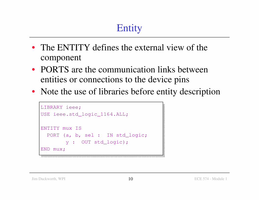
Entity
• The ENTITY defines the external view of the component
• PORTS are the communication links between entities or connections to the device pins
• Note the use of libraries before entity description
LIBRARY ieee;
USE ieee.std_logic_1164.ALL;
ENTITY mux IS
PORT (a, b, sel : IN std_logic;
y : OUT std_logic);
END mux;

Jim Duckworth, WPI ECE 574 - Module 111
Architecture
• The ARCHITECTURE defines the function or behavior or
structure of the ENTITY
• Consists of concurrent statements, e.g.
– Process statements
– Concurrent Signal Assignment statements
– Conditional Signal Assignment statements
• An entity may have several architectures
ARCHITECTURE behavior OF mux IS
BEGIN
y <= a WHEN sel = ‘0’ ELSE
b;
END behavior;
Jim Duckworth, WPI ECE 574 - Module 112
VHDL Notes
• There is no explicit reference to actual hardware
components
– There are no D-type flip-flops, mux, etc
– Required logic is inferred from the VHDL description
– Same VHDL can target many different devices
• There are many alternative ways to describe the required
behavior of the final system
– Exactly the same hardware will be produced
– Some ways are more intuitive and easier to read
• Remember that the synthesis tools must be able to deduce
your intent and system requirements
– For sequential circuits it is usually necessary to follow
recommended templates and style

Jim Duckworth, WPI ECE 574 - Module 113
Programmable Logic Devices
• Xilinx user programmable devices
– FPGAs – Field Programmable Gate Array
• Virtex 4, Virtex 5, Virtex 6, and Virtex 7
• Spartan 3, Spartan 6
• Consist of configurable logic blocks
– Provides look-up tables to implement logic
– Storage devices to implement flip-flops and latches
– CPLDs – Complex Programmable Logic Devices
• CoolRunner-II CPLDS (1.8 and 3.3 volt devices)
• XC9500 Series (3.3 and 5 volt devices)
• Consist of macrocells that contain programmable and-or matrix with
flip-flops
• Altera has a similar range of devices
Jim Duckworth, WPI ECE 574 - Module 114
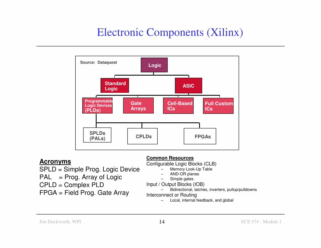
Electronic Components (Xilinx)
Source: DataquestLogic
StandardLogic
ASIC
ProgrammableLogic Devices
(PLDs)
GateArrays
Cell-BasedICs
Full CustomICs
CPLDsSPLDs(PALs) FPGAs
Acronyms
SPLD = Simple Prog. Logic Device
PAL = Prog. Array of Logic
CPLD = Complex PLD
FPGA = Field Prog. Gate Array
Common ResourcesConfigurable Logic Blocks (CLB)
– Memory Look-Up Table
– AND-OR planes
– Simple gates
Input / Output Blocks (IOB)– Bidirectional, latches, inverters, pullup/pulldowns
Interconnect or Routing– Local, internal feedback, and global
Jim Duckworth, WPI ECE 574 - Module 115
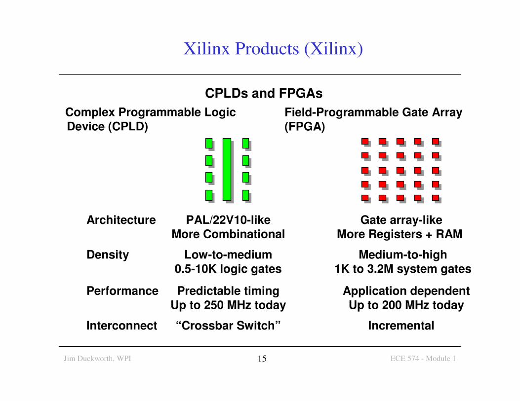
Xilinx Products (Xilinx)
CPLDs and FPGAs
Architecture PAL/22V10-like Gate array-like
More Combinational More Registers + RAM
Density Low-to-medium Medium-to-high0.5-10K logic gates 1K to 3.2M system gates
Performance Predictable timing Application dependent
Up to 250 MHz today Up to 200 MHz today
Interconnect “Crossbar Switch” Incremental
Complex Programmable Logic
Device (CPLD)
Field-Programmable Gate Array
(FPGA)
Jim Duckworth, WPI ECE 574 - Module 116
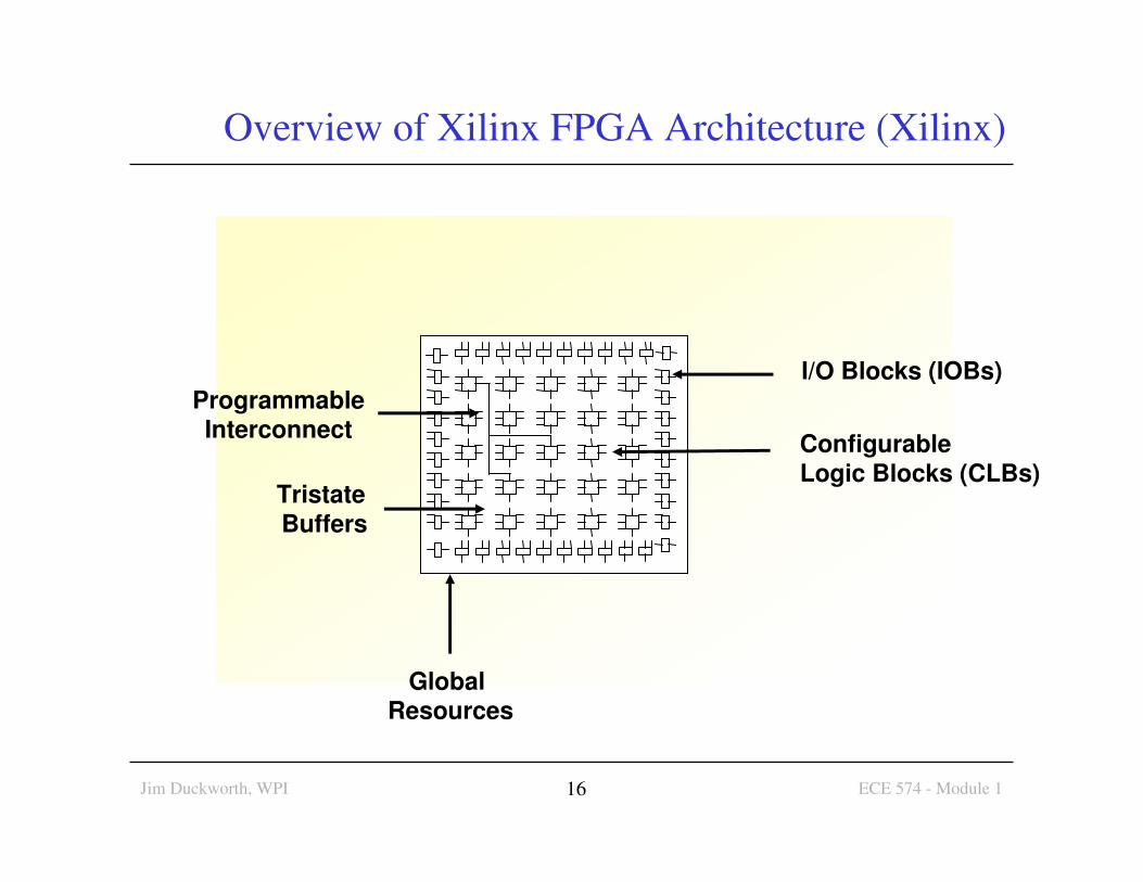
Overview of Xilinx FPGA Architecture (Xilinx)
ProgrammableInterconnect
I/O Blocks (IOBs)
ConfigurableLogic Blocks (CLBs)
Tristate Buffers
Global Resources
Jim Duckworth, WPI ECE 574 - Module 117
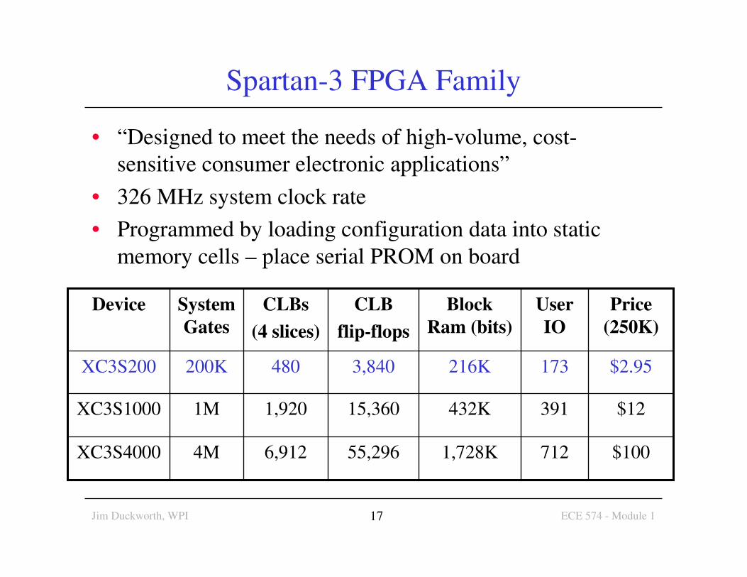
Spartan-3 FPGA Family
• “Designed to meet the needs of high-volume, cost-
sensitive consumer electronic applications”
• 326 MHz system clock rate
• Programmed by loading configuration data into static
memory cells – place serial PROM on board
55,296
15,360
3,840
CLB
flip-flops
$1007121,728K6,9124MXC3S4000
$12391432K1,9201MXC3S1000
$2.95173216K480200KXC3S200
Price
(250K)
User
IO
Block
Ram (bits)
CLBs
(4 slices)
System
Gates
Device
Jim Duckworth, WPI ECE 574 - Module 118
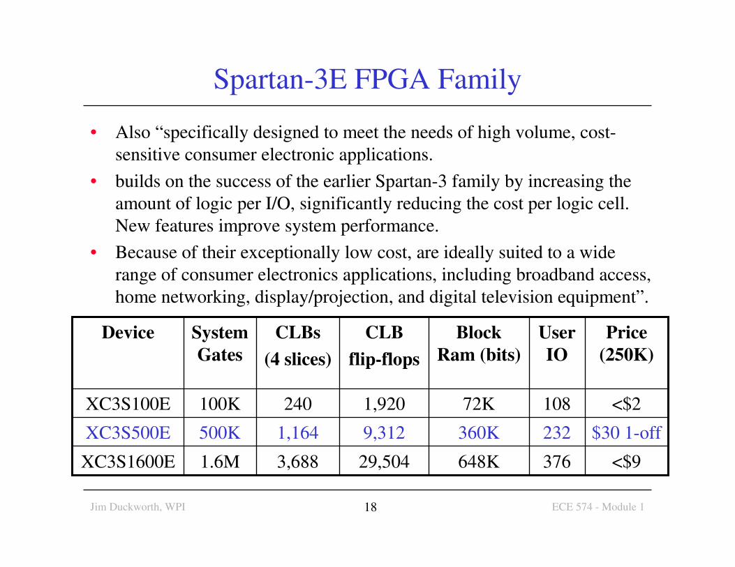
Spartan-3E FPGA Family
• Also “specifically designed to meet the needs of high volume, cost-
sensitive consumer electronic applications.
• builds on the success of the earlier Spartan-3 family by increasing the
amount of logic per I/O, significantly reducing the cost per logic cell.
New features improve system performance.
• Because of their exceptionally low cost, are ideally suited to a wide
range of consumer electronics applications, including broadband access,
home networking, display/projection, and digital television equipment”.
29,504
9,312
1,920
CLB
flip-flops
<$9376648K3,6881.6MXC3S1600E
$30 1-off232360K1,164500KXC3S500E
<$210872K240100KXC3S100E
Price
(250K)
User
IO
Block
Ram (bits)
CLBs
(4 slices)
System
Gates
Device
Jim Duckworth, WPI ECE 574 - Module 119
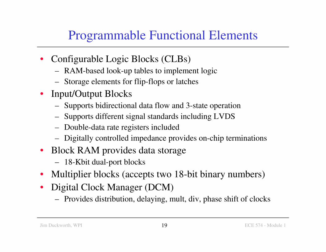
Programmable Functional Elements
• Configurable Logic Blocks (CLBs)– RAM-based look-up tables to implement logic
– Storage elements for flip-flops or latches
• Input/Output Blocks– Supports bidirectional data flow and 3-state operation
– Supports different signal standards including LVDS
– Double-data rate registers included
– Digitally controlled impedance provides on-chip terminations
• Block RAM provides data storage – 18-Kbit dual-port blocks
• Multiplier blocks (accepts two 18-bit binary numbers)
• Digital Clock Manager (DCM)– Provides distribution, delaying, mult, div, phase shift of clocks
Jim Duckworth, WPI ECE 574 - Module 120
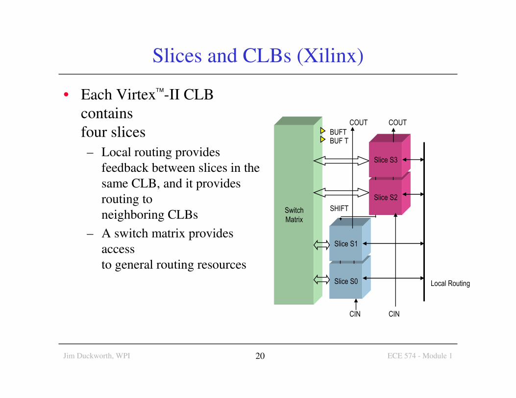
Slices and CLBs (Xilinx)
• Each Virtex-II CLB
contains
four slices
– Local routing provides
feedback between slices in the
same CLB, and it provides
routing to
neighboring CLBs
– A switch matrix provides
access
to general routing resources
CIN
Switch
Matrix
BUFTBUF T
COUTCOUT
Slice S0
Slice S1
Local Routing
Slice S2
Slice S3
CIN
SHIFT

Jim Duckworth, WPI ECE 574 - Module 121
Slice 0
LUT Carry
LUT Carry D Q
CE
PRE
CLR
DQCE
PRE
CLR
Simplified Slice Structure (Xilinx)
• Each slice has four outputs
– Two registered outputs,
two non-registered outputs
– Two BUFTs associated
with each CLB, accessible
by all 16 CLB outputs
• Carry logic runs vertically,
up only
– Two independent
carry chains per CLB

Jim Duckworth, WPI ECE 574 - Module 122
Detailed Slice Structure (Xilinx)
• The next slides will
discuss the slice
features
– LUTs
– MUXF5, MUXF6,
MUXF7, MUXF8
(only the F5 and
F6 MUX are shown
in the diagram)
– Carry Logic
– MULT_ANDs
– Sequential Elements

Jim Duckworth, WPI ECE 574 - Module 123
Combinatorial Logic
AB
CD
Z
Look-Up Tables (Xilinx)
• Combinatorial logic is stored in Look-Up Tables (LUTs)
– Also called Function Generators (FGs)
– Capacity is limited by number of inputs, not complexity
• Delay through the LUT is constant
11111
00111
01011
00011
...
11010
10010
11100
00100
01000
00000
ZDCBA
Jim Duckworth, WPI ECE 574 - Module 124
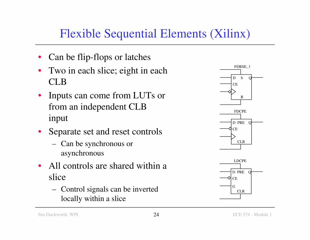
Flexible Sequential Elements (Xilinx)
• Can be flip-flops or latches
• Two in each slice; eight in each
CLB
• Inputs can come from LUTs or
from an independent CLB
input
• Separate set and reset controls
– Can be synchronous or
asynchronous
• All controls are shared within a
slice
– Control signals can be inverted
locally within a slice
D
CE
PRE
CLR
Q
FDCPE
D
CE
S
R
Q
FDRSE
D
CE
PRE
CLR
Q
LDCPE
G
_1

Jim Duckworth, WPI ECE 574 - Module 125
IOB Element (Xilinx)
• Input path
– Two DDR registers
• Output path
– Two DDR registers
– Two 3-state enable
DDR registers
• Separate clocks and
clock enables for I and O
• Set and reset signals
are shared
Reg
Reg
DDR MUX
3-state
OCK1
OCK2
Reg
Reg
DDR MUX
Output
OCK1
OCK2
PAD
Reg
Reg
Input
ICK1
ICK2
IOB
Jim Duckworth, WPI ECE 574 - Module 126
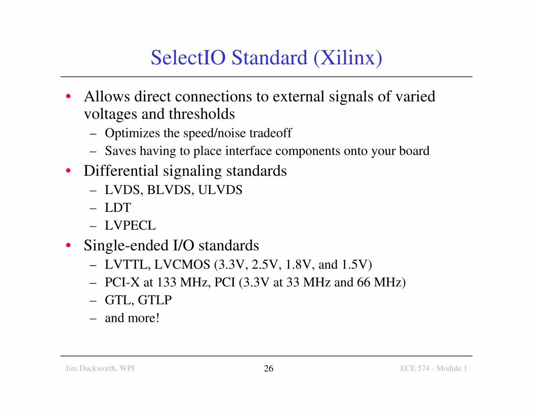
SelectIO Standard (Xilinx)
• Allows direct connections to external signals of varied voltages and thresholds– Optimizes the speed/noise tradeoff
– Saves having to place interface components onto your board
• Differential signaling standards– LVDS, BLVDS, ULVDS
– LDT
– LVPECL
• Single-ended I/O standards– LVTTL, LVCMOS (3.3V, 2.5V, 1.8V, and 1.5V)
– PCI-X at 133 MHz, PCI (3.3V at 33 MHz and 66 MHz)
– GTL, GTLP
– and more!
Jim Duckworth, WPI ECE 574 - Module 127
Digital Controlled Impedance (DCI)
• DCI provides
– Output drivers that match the impedance of the traces
– On-chip termination for receivers and transmitters
• DCI advantages
– Improves signal integrity by eliminating stub reflections
– Reduces board routing complexity and component count by
eliminating external resistors
– Internal feedback circuit eliminates the effects of temperature,
voltage, and process variations

Jim Duckworth, WPI ECE 574 - Module 128
Block SelectRAM Resources (Xilinx)
• Up to 3.5 Mb of RAM in 18-
kb blocks
– Synchronous read and write
• True dual-port memory
– Each port has synchronous read
and write capability
– Different clocks for each port
• Supports initial values
• Synchronous reset on output
latches
• Supports parity bits
– One parity bit per eight data
bits
Jim Duckworth, WPI ECE 574 - Module 129
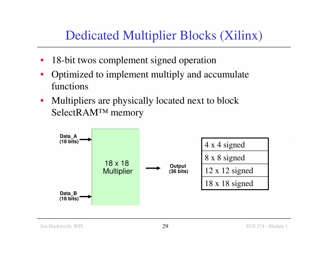
Dedicated Multiplier Blocks (Xilinx)
• 18-bit twos complement signed operation
• Optimized to implement multiply and accumulate
functions
• Multipliers are physically located next to block
SelectRAM™ memory
18 x 18Multiplier
Output (36 bits)
Data_A (18 bits)
Data_B (18 bits)
18 x 18 signed
12 x 12 signed
8 x 8 signed
4 x 4 signed
Jim Duckworth, WPI ECE 574 - Module 130
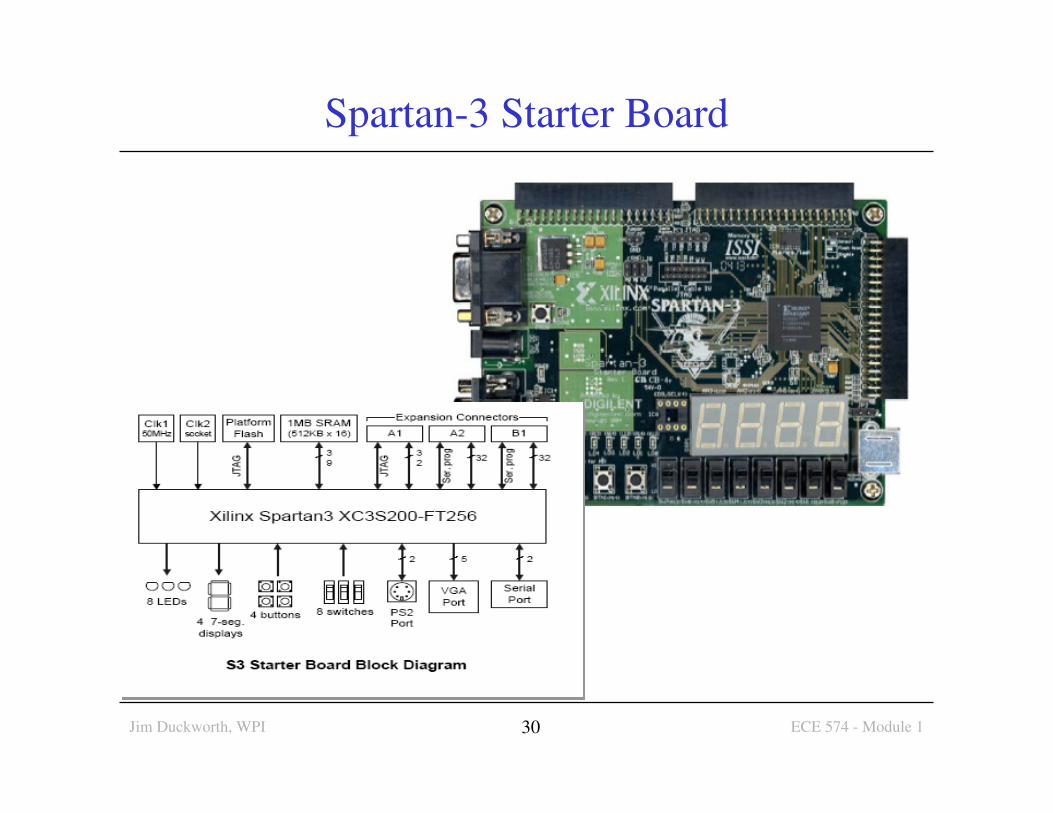
Spartan-3 Starter Board

Jim Duckworth, WPI ECE 574 - Module 131
Nexys 2 Board ($99)

Jim Duckworth, WPI ECE 574 - Module 132
Logic Synthesis
• A process which takes a digital circuit description and
translates it into a gate level design, optimized for a
particular implementation technology.
Jim Duckworth, WPI ECE 574 - Module 133
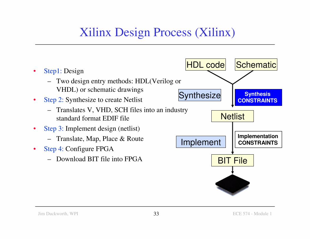
Xilinx Design Process (Xilinx)
• Step1: Design
– Two design entry methods: HDL(Verilog or
VHDL) or schematic drawings
• Step 2: Synthesize to create Netlist
– Translates V, VHD, SCH files into an industry
standard format EDIF file
• Step 3: Implement design (netlist)
– Translate, Map, Place & Route
• Step 4: Configure FPGA
– Download BIT file into FPGA
HDL code Schematic
Netlist
Implement
Synthesize
BIT File
SynthesisCONSTRAINTS
ImplementationCONSTRAINTS
Jim Duckworth, WPI ECE 574 - Module 134
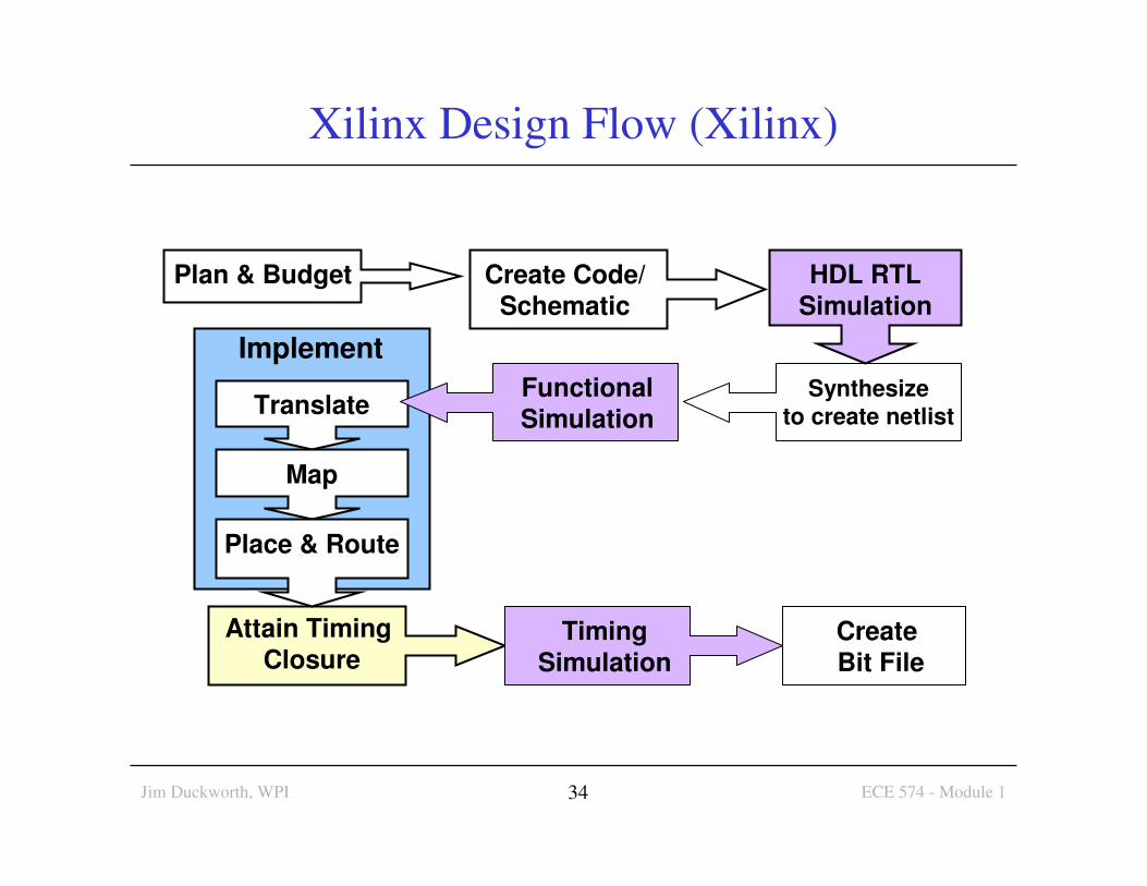
Translate
Map
Place & Route
Xilinx Design Flow (Xilinx)
Plan & Budget HDL RTLSimulation
Synthesize
to create netlist
Functional
Simulation
Create
Bit File
Attain Timing
ClosureTiming
Simulation
Implement
Create Code/Schematic

Jim Duckworth, WPI ECE 574 - Module 135
Program the FPGA (Xilinx)
• There are three ways to
program an FPGA
– Through a PROM device
• You will need to generate a
file that the PROM
programmer will understand
– Directly from the computer
• Use the iMPACT
configuration tool
• (need JTAG)
– Use USB connector
• Digilent Adept tool
Jim Duckworth, WPI ECE 574 - Module 136
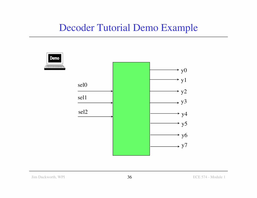
Decoder Tutorial Demo Example
sel0
sel1
y0
y1
y2
y3
y4
y5
y6
y7
sel2

Jim Duckworth, WPI ECE 574 - Module 137
VHDL Source Code

Jim Duckworth, WPI ECE 574 - Module 138
Synthesizing the Design
=========================================================================
* HDL Synthesis *
=========================================================================
Synthesizing Unit <decoder>.
Related source file is "C:/ee574/nexsys2/decoder/decoder.vhd".
Found 1-of-8 decoder for signal <y>.
Summary:
inferred 1 Decoder(s).
Unit <decoder> synthesized.

Jim Duckworth, WPI ECE 574 - Module 139
View the Schematic Representation

Jim Duckworth, WPI ECE 574 - Module 140
Decoder Implemented on FPGA

Jim Duckworth, WPI ECE 574 - Module 141
Zooming in on Logic Slice

Jim Duckworth, WPI ECE 574 - Module 142
Assigning Package Pins

Jim Duckworth, WPI ECE 574 - Module 143
New Implementation to Match Target

Jim Duckworth, WPI ECE 574 - Module 144
Verilog Background
• 1983: Gateway Design Automation released Verilog HDL
“Verilog” and simulator
• 1985: Verilog enhanced version – “Verilog-XL”
• 1987: Verilog-XL becoming more popular (same year
VHDL released as IEEE standard)
• 1989: Cadence bought Gateway
• 1995: Verilog adopted by IEEE as standard 1364
– Verilog HDL, Verilog 1995
• 2001: First major revision (cleanup and enhancements)
– Standard 1364-2001 (or Verilog 2001)
• System Verilog under development
Jim Duckworth, WPI ECE 574 - Module 145
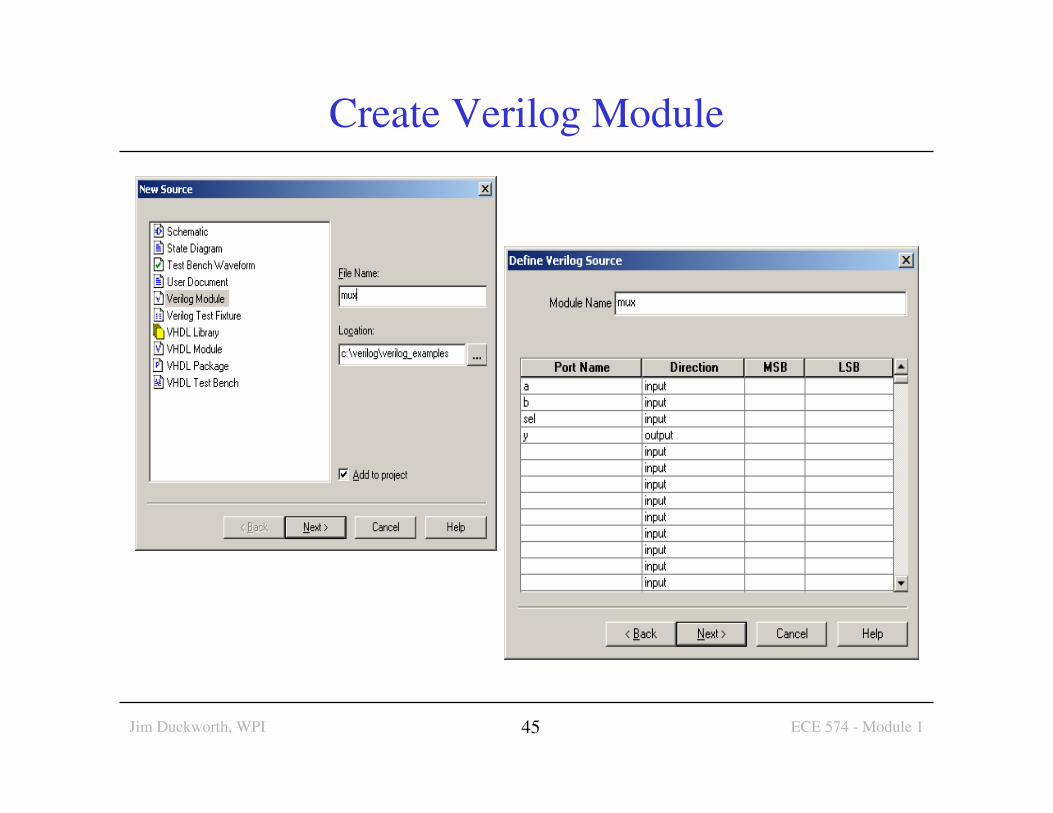
Create Verilog Module

Jim Duckworth, WPI ECE 574 - Module 146
Module Created
• No separate entity and arch –
just module
• Ports can be input, output, or
inout
• Note: Verilog 2001 has
alternative port style:– (input a, b, sel, output y);

Jim Duckworth, WPI ECE 574 - Module 147
Add Assign Statement
• Similar to VHDL conditional signal assignment – continuous assignment
• Exactly same hardware produced
Jim Duckworth, WPI ECE 574 - Module 148
Verilog - General Comments
• VHDL is like ADA and Pascal in style• Strongly typed – more robust
• Verilog is more like the ‘C’ language
• Verilog is case sensitive
• White space is OK (tabs, new lines, etc)
• Statements terminated with semicolon (;)
• Verilog statements between• module and endmodule
• Comments // single line and /* and */

Jim Duckworth, WPI ECE 574 - Module 149
Verilog Logic
• Four-value logic system
• 0 – logic zero, or false condition
• 1 – logic 1, or true condition
• x, X – unknown logic value
• z, Z - high-impedance state
• Number formats
• b, B binary
• d, D decimal (default)
• h, H hexadecimal
• o, O octal
• 16’H789A – 16-bit number in hex format
• 1’b0 – 1-bit
Jim Duckworth, WPI ECE 574 - Module 150
Verilog and VHDL – Reminder
• VHDL - like Pascal and Ada programming languages
• Verilog - more like ‘C’ programming language
• But remember they are Hardware Description Languages -
They are NOT programming languages
– FPGAs do NOT contain an hidden microprocessor or interpreter or
memory that executes the VHDL or Verilog code
– Synthesis tools prepare a hardware design that is inferred from the
behavior described by the HDL
– A bit stream is transferred to the programmable device to configure
the device
– No shortcuts! Need to understand combinational/sequential logic
• Uses subset of language for synthesis
• Check - could you design circuit from description?