vision processing with the canny edge detection … information • uncanny vision, canny edge...
TRANSCRIPT

Vision Processing with the Canny Edge DetectionReference Design
2015-02-14
AN-732 Subscribe Send Feedback
About Canny Edge DetectionCanny edge detection is a multistage, vision processing algorithm producing a binary output image (edgeor no edge for complex vision algorithms such as number plate identification). Canny edge detection canremove irrelevant image information and has a simple binary output for each pixel.Traditionally, Cannyedge detection is implemented on high-performance computing. However, you can now implementvision algorithms on embedded platforms for mobile low-power applications.
Vision algorithms such as Canny contain multiple processing stages. Typically processors have to fetchthe input image frame from external memory, process it, and write it back to external memory. Theprocessor repeats this process for the next processing block. This traditional memory shuffling betweenblocks is inefficient:
• Repeated slow external memory access causes speed bottlenecks. The data has to propagate throughthe processor caches, further slowing down external memory access due to cache overheads.
• Repeatedly engergizing the external memory chip I/O pins costs dynamic power.
About the Canny Edge Detection Reference DesignThe Altera® Canny edge detection reference design targets a Cyclone® V SoC, which contains an AlteraCyclone V FPGA and a dual core ARM® Cortex A9 hard processor system (HPS). This design partitionsthe Canny edge detection across the FPGA and ARM processor, using the FPGA as a hardwareaccelerator. The ARM processor runs the software algorithms, which are easier to execute in software thanin hardware.
Using the Cyclone V SoC boosts performance and lowers power consumption. The flexibility of thereference design allows you to develop other custom applications around it.
FPGAs offer the most optimal solution. FPGAs use stream-based processing that produces an outputpixel as each input pixel arrives. This approach is suitable for common image pre-processing operationssuch as two dimensional convolution and monochrome conversion. The reference design's customhardware implementation results in minimal logic utilization and very little on-chip FPGA memoryusage, which gives a fast and power-efficient design architecture. The design can chain the stream-basedprocessing blocks together. Internal FPGA voltages for RTL blocks are small as compared to I/O voltages,which gives power savings.
© 2015 Altera Corporation. All rights reserved. ALTERA, ARRIA, CYCLONE, ENPIRION, MAX, MEGACORE, NIOS, QUARTUS and STRATIX words and logos aretrademarks of Altera Corporation and registered in the U.S. Patent and Trademark Office and in other countries. All other words and logos identified astrademarks or service marks are the property of their respective holders as described at www.altera.com/common/legal.html. Altera warrants performanceof its semiconductor products to current specifications in accordance with Altera's standard warranty, but reserves the right to make changes to anyproducts and services at any time without notice. Altera assumes no responsibility or liability arising out of the application or use of any information,product, or service described herein except as expressly agreed to in writing by Altera. Altera customers are advised to obtain the latest version of devicespecifications before relying on any published information and before placing orders for products or services.
ISO9001:2008Registered
www.altera.com101 Innovation Drive, San Jose, CA 95134
Related Information
• Uncanny Vision, Canny edge detection on ARM• Andre Silva, Embedded Image Processing - Canny Edge Detector running on i.MX51 Freescale's
ARM Processor,
Getting Started with the Canny Edge Reference Design
Hardware and Software RequirementsObtain the hardware and install all software before you use the Canny edge reference design
Hardware:
• Altera Cyclone V SoC Development Kit• Digital video interface (DVI) source• DVI monitor
Software:
• Quartus II software version 14.0• The MATLAB image processing suite (optional)• Linux version 3.9.0
Connecting the Hardware to Use the Canny Edge Reference Design1. Connect the following hardware to the Cyclone V SoC development board:
• UART for ARM processor• Power supply• USB JTAG cable• Ethernet cable for ARM processor• DVI output and DVI input cables
Loading the Canny Edge Reference Design FPGA Image with the SD Card Image1. Write the reference design SD card image to a microSD card:
#sudo dd if=Canny_sdcard_image of=/dev/sdx bs=1M#sudo sync
After a successful Linux boot, the FPGA image automatically loads.2. Set the DIP switches to select the output from one of the Canny blocks. If there is no video output,
disconnect the DVI source cable from the BITEC card, reconnect the DVI source cable wire.
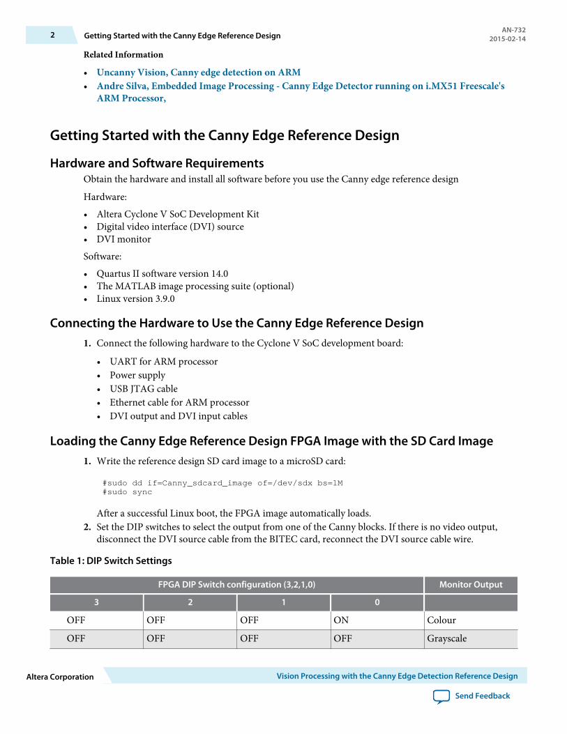
Table 1: DIP Switch Settings
FPGA DIP Switch configuration (3,2,1,0) Monitor Output
3 2 1 0
OFF OFF OFF ON Colour
OFF OFF OFF OFF Grayscale
2 Getting Started with the Canny Edge Reference DesignAN-732
2015-02-14
Altera Corporation Vision Processing with the Canny Edge Detection Reference Design
Send Feedback

FPGA DIP Switch configuration (3,2,1,0) Monitor Output
3 2 1 0
OFF OFF ON OFF Sobel
OFF ON OFF OFF NMS
ON OFF OFF OFF DoubleThreshold
ON ON OFF OFF ARM output
ON ON ON OFF Approximated 45degree edge anglecolour codedoutput
OFF OFF ON ON Blue colorchannel only
OFF ON OFF ON Green colorchannel only
ON OFF OFF ON Red colorchannel only
3. Type root to login. You do not need a password.4. Press the FPGA 0 push button to activate the ARM frame reader. FPGA LED 3 illuminates.5. Press FPGA 1 push button to activate the ARM frame writer. FPGA LED 2 illuminates.
The frame reader and writer cannot be running during the boot process.6. Navigate to the altera folder, and type ./edge_link into the terminal to start the edge linking program.
Table 2: Files in /altera Directory
File name Description Example use
edge_link Edge linking program for Cannyedge detection
./edge_link
dumpram Dumps an image frame into theLinux filesystem
./dumpram
pass_thru Does a simple ARM video loopthrough without any processing
./pass_thru
devmem3 Tool to peak and poke the physicalmemory contents in the ARMprocessor
./devmem3 r 0xff200000 0x0
(Read, Physical address, Addressoffset)
./devmem3 w 0xff200000 0x00x1
(Read, Physical address, Addressoffset, write value)
AN-7322015-02-14 Loading the Canny Edge Reference Design FPGA Image with the SD Card Image 3
Vision Processing with the Canny Edge Detection Reference Design Altera Corporation
Send Feedback

File name Description Example use
burn_fpga Script to program the FPGA fromLinux
./burn_fpga canny_fpga.rbf
gator.ko Linux kernel module for ARM DS5streamline
Note: Only works for v3.9.0
insmod gator.ko
gatord Linux kernel daemon for ARM DS5streamline Linux profiling
./gatord.ko&
7. If image is not centred on the monitor, press the CPU reset button and repeat from #dmi1421333866870.xml/step_N1018C_N10011_N1000E_N10001.
Canny Edge Reference Design Initial Startup Problems
Table 3: Initial Startup Problems
Problem Solution
Monitor output is black Remove the DVI transmitter cable and reinsert it.Monitor output is fuzzy Press the CPU reset button to reset the FPGA design. Press the
reset button until synchronization is achieved (i.e. video issharp).
Controlling the FPGA Flow of the Canny Edge Reference DesignUse the System Console in the Quartus® II software to control the flow.
1. Open System console.2. Run the gui_thres_res.tcl script.
The drop down menu selects the type of video data to be passed into the ARM.
Note: Select the first drop down menu item if running the edge_linking algorithm.
Capturing the Pixel Stream
Before you begin
Ensure the FPGA image is loaded, the ARM is correctly configured, and the frame reader is running.
1. From the System Console GUI, select the video type to be passed into the ARMAn uncompressed frame image file ARMvideo_frame.dat is now in the Linux file system
2. Export this file to your PC that is running MATLAB.3. Run the MATLAB script parse_dat2 to convert the uncompressed .dat file to a viewable image:
parse_dat2(<image length>,<image height>,<.dat file name>,0)
4 Canny Edge Reference Design Initial Startup ProblemsAN-732
2015-02-14
Altera Corporation Vision Processing with the Canny Edge Detection Reference Design
Send Feedback

Programming the FPGA with the Canny Edge Reference Design
Before you begin
Ensure the ARM processor completes its boot process before programming the FPGA.
1. Load the FPGA image from the Quartus II programmer: Tools > Programmer.2. Program the file top.sof
3. To program the FPGA from the ARM processor:
Note: Do not program the FPGA from the ARM processor if the ARM processor already has an FPGAimage loaded.
a. Ensure all MSEL dip switches are in the ON position.b. Ensure the program burn_fpga is available.c. Ensure the FPGA image canny_fpga.rbf is available.
root@socfpga:~/altera# ./burn_fpga canny_fpga.rbfBurning FPGA image file canny_fpga.rbfEnsure all MSEL DIP switches are ON13685+1 records in13685+1 records outFPGA image burned from SD card!ARM-FPGA bridges are enabled!
FPGA LED 0 and 1 are now ON to indicate that the FPGA is running.
Initializing the ARM ProcessorInitialize the ARM processor, if the FPGA is not configured during U-boot.
1. Program the FPGA using the Quartus II software or the burn_fpga tool after the ARM boot processcompletes.
2. Press the WARM reset button to reboot Linux without erasing the loaded FPGA design, which initial‐izes the FPGA HPS SDRAM interface correctly. Only initialize it during the boot process with anFPGA image running.
3. If using Altera’s GSRD Linux Distro, kill the scroll server application, which may interfere with theframe reader and writera. Type ps to get a list of the currently running processes.b. Find the process ID number of the scroll server application.c. Kill scroll server by typing kill <PID number>
4. Press the FPGA 0 Push button to activate the ARM Frame reader.FPGA LED 3 illuminates.
5. Press FPGA 1 push button to activate the ARM frame writer.The Frame reader and writer cannot be running during the boot process. If synchronization is off,press the CPU reset button and repeat from step 4.FPGA LED 2 illuminates.
AN-7322015-02-14 Programming the FPGA with the Canny Edge Reference Design 5
Vision Processing with the Canny Edge Detection Reference Design Altera Corporation
Send Feedback

Canny Edge Detection Reference Design Block DescriptionFigure 1: Block Diagram
VideoInput
GrayscaleConversion
GaussianFilter
SobelFilter
NonmaximalSuppression
DoubleThreshold
EdgeLink
VideoOutput
Cache
External DDR3 SDRAM
SlowInefficient Architecture
Power Inefficient
Traditional Processor-Based Implementation
VideoInput
GrayscaleConversion
GaussianFilter
SobelFilter
NonmaximalSuppression
DoubleThreshold
EdgeLink
VideoOutput
Cache
External DDR3 SDRAM
FastEfficient Architecture
Power Efficient
FPGA-Processor Implementation
The design matches the output pixel rate to the input pixel rate, easily achieving real time requirements of60 fps. However, the maximum frequency (fMAX) of the individual blocks limits the maximum video inputresolution. Implementing most of the Canny algorithm on the FPGA offloads the ARM processor fromrepetitive and time consuming mathematical operations. Thus, the ARM processor engages in morecomplicated, upstream, higher value image processing algorithms. For example, the design implementsthe last Canny edge linking block in the ARM processor because it is a recursive variable depth algorithmthat cannot be unrolled.
Greyscale ConversionEdge detection algorithms operate on one color channel. The video input has three color channels, so thedesign converts it to grayscale.
The design uses the NTSC standard color space to convert. The design avoids using complex floating-point hardware, which limits fMAX performance and introduces clock cycle latency if pipelining is used toincrease fmax performance. The design uses bit-slice method to simplify floating point calculations whereprecision is not required. However, this method can only be used if the coefficients are constant.
6 Canny Edge Detection Reference Design Block DescriptionAN-732
2015-02-14
Altera Corporation Vision Processing with the Canny Edge Detection Reference Design
Send Feedback

Figure 2: Greyscale
Gaussian BlurringCanny edge detection is very sensitive to noise. The design uses a two dimensional Gaussian filter to blurthe grayscale output image
A Gaussian filter is a low pass filter that attenuates high frequency noise. By convolving the image matrixwith the Gaussian kernel, the design smudges the image as each individual output pixel is the weightedGaussian average of its surrounding pixels (spatial weighted averaging). To obtain the discrete Gaussiankernel coefficients, the design determines the kernel size and chooses the appropriate standard deviationfrom the continuous 2D Gaussian equation. Implementing 2D convolution in hardware is similar to thatof 1D convolution. Both cases use a tapped delay line. However the 2D case needs to delay an entire videoline to access the previous matrix row entry using FIFO buffers. For previous column entries, the designuses register delay lines. Hence, a FIFO buffer implements row delays; registers implement column delays.
Figure 3: Gaussian Blurring
Sobel Edge IntensityThe design applies a Sobel operator to extract the image gradient intensity. Canny edge detection oftenuses a Sobel operator as its kernel weights have a degree of noise suppression.
The Sobel output is a 2D vector matrix in which its magnitude represents edge intensity strength and itsdirection indicates the orientation of the edge direction.
AN-7322015-02-14 Gaussian Blurring 7
Vision Processing with the Canny Edge Detection Reference Design Altera Corporation
Send Feedback

For more information: Rafael C. Gonzalez, Richard E. Woods Digital Image Processing Second Edition,2nd ed., Prentice Hall pp.577-578 andl pp.579
The edge magnitude may exceed the maximum 8 bit pixel value of 255 so the design saturates the edgeoutput pixel to 255 rather than normalizing, which does not give a very bright image output. Thus theSobel output flushed to the monitor screen is saturated. The subsequent Canny blocks use the full Sobeloutput bit range for maximum precision.
Figure 4: Sobel Output
Nonmaximal SuppressionSobel edges tend to be quite thick because of the range of edge intensity values present. Thick edges arenot desirable for Canny edge detection as it contains redundant information, slowing down processing forthe edge-linking block as more strong-weak edge comparisons have to be made for the recursive grass-firealgorithm. Thin line edges are desirable. Nonmaximal suppression gives thin edges. This block traces theedges along its edge direction and sets any edge value that is non-maximal to 0.
For ease of implementation the hardware makes a localized search in a 3x3 window. As edge tracingoccurs in an 8-point connected region, the design only uses only approximated edge angles of 45 degrees:0, 45, 90 and 135. The 3x3 region is obtained using the same tapped delay line method used in theGaussian and Sobel blocks.
Figure 5: Nonmaximal Suppression Output
Shows thinned out edges.
8 Nonmaximal SuppressionAN-732
2015-02-14
Altera Corporation Vision Processing with the Canny Edge Detection Reference Design
Send Feedback

Double ThresholdApplying a double threshold classifies edge pixels from the nonmaximal suppression output as not anedge, weak edge or strong edge.
Some of the edge pixels might be caused by noise and color variations or texturing artefacts. The designuses two thresholds to discern between a true edge and a pseudo edge. The design classifies pixel edgeintensities below the low threshold value as not an edge; those between the low and high threshold asweak edges. The design classifies those above the high threshold value as strong edges. The design givesstrong edge pixels the maximum value of 255; weak edge pixels the high threshold value. Pixels that thedesign reclassifies as not an edge are suppressed to 0.
Edge LinkingThe double threshold output often suffers from streaking where weak edge pixels break up strong edgepixels, because it is difficult to choose the perfect low and high threshold values. Some true edge pixelsmay be classified as weak edge pixels as their values might fluctuate around the high threshold. The designcan reclassify the weak edge pixels as strong edge if they are connected to a strong edge pixel eitherdirectly or indirectly. An indirect connection is defined as a weak edge pixel linked to a strong edge viacontinuously connecting weak edge pixels. Weak edge pixels not connected to any strong pixels arereclassified as no edge pixels. True edges form continuous lines and any rogue weak edges because ofnoise and color variations or texturing effects are independently distributed from true edges. The designperforms strong-weak edge linking recursively as its connection end points and depth are variable.
The design:
• Scans the double threshold image pixel by pixel until the last image pixel is reached.• If a strong edge pixel is encountered, checks its immediate 8 point connected neighborhood for any
weak edge pixel.• If it finds a pixel neighbor with a weak edge intensity, burns that neighboring pixel as a strong edge.
Returns to step 2 on that neighboring pixel (the recursive step). Thus effectively burning any weakedge pixels connected to a strong edge pixel.
The design reaches the recursive end point when it finds no more neighboring weak edge or when itreaches the image boundaries. The design implements this recursive algorithm in software in the ARMprocessor. Edge-linking is memory based: an entire video frame is available in memory for processing.
Figure 6: Edge Linking Output
Shows streaking eliminated and rogue pixels suppressed.
AN-7322015-02-14 Double Threshold 9
Vision Processing with the Canny Edge Detection Reference Design Altera Corporation
Send Feedback

Stream-to-Memory ConversionThe Canny edge reference design FPGA processing architecture is stream based: an output pixel isproduced for every input pixel. Edge-linking is memory based: an entire video frame is available inmemory for processing. The design implements a stream to memory conversion to reorder the FPGApixel stream into a proper video frame in memory for the ARM processor. After the ARM processes anentire video frame, the design streams it from memory to the FPGA for the output monitors to receivepixel streams.
Figure 7: Clock Domains
HPS SDRAMmSGDMAMemory to
StreamDual-Clock FIFO
Input Data
Input Clock
Output Clock
Output Data Canny OutputPixel Stream
mSGDMAStream toMemory
Dual-Clock FIFO
Data
Clock
Clock
Output Data Stream toMemory
Memoryto Stream
SDRAM Clock Domain
ARM(Edge Linking)
FPGA Double-ThresholdOutput Pixel Stream
clk_dvi
fpga_clk
clk_dvi
fpga_clk
FPGA-ARM Video Handover ARM-FPGA Video Handover
Clock DomainCrossing
Clock DomainCrossing
DVI Clock Domain FPGA Clock Domain DVI Clock Domain
FPGA and ARM Processor Clock DomainsBoth clock domains in the Canny edge reference design use the Qsys Modular Scatter-Gather DirectMemory Access controller (mSGDMA) soft IP core.For the stream-to-memory conversion, themSGDMA increments the memory address by one 32-bit word address and stores the input pixel in thataddress for each pixel received. The start address and length of transfer are set by the FPGA by writing tothe appropriate control registers of the mSGDMA. The transfer length is the total number of pixels in avideo. The reverse mSGDMA memory-to-stream conversion is similar. The FPGA provides the startmemory address and number of memory entries to convert into a pixel stream.
The Qsys components are in the fixed FPGA 50 MHz clock domain. The design uses digital videointerface (DVI) and its clock frequency varies according to video resolution. Because the pixel streams arein the clk_dvi domain, the design uses a dual clocked FIFO buffer for proper data clock domainbridging. Using a FIFO buffer buffers the pixel data.
The FPGA pixel stream is not continuous as it pauses when the data enable signal is active low. For DVI,pixel data are only latched when the DE control signal is active high. Furthermore, the mSGDMA operatesusing burst transactions as the HPS SDRAM multiport front end (MPFE) controller may be busyservicing other requests. For example when the ARM processor reads or writes from memory. Hence, abuffer ensures that no pixel data is lost. The design allows no backpressure to occur. For the stream-to-memory FIFO clock domain bridging buffer, the fill rate is determined by the input pixel stream out ofthe FPGA Canny double threshold block. The output rate is determined by the mSGDMA stream tomemory transaction rate.
10 Stream-to-Memory ConversionAN-732
2015-02-14
Altera Corporation Vision Processing with the Canny Edge Detection Reference Design
Send Feedback

HPS SDRAM PartitionsThe Canny edge reference design uses the HPS SDRAM to boost data throughput and improve processingtime.
Getting the frame data from the FPGA SDRAM via the FPGA-ARM AXI connection bus requires nooverheads.. The design runs a Linux operating system on the ARM processor and it partitions the HPSSDRAM to provide mutually exclusive access for the FPGA and the ARM processor. The design does notallow the FPGA to write into the Linux address space, which may cause Linux to crash during run-time.The design assigns the top 512 MB of the HPS SDRAM to Linux; the bottom 512 MB for private access bythe FPGA for frame buffering.
Frame BufferingThe Canny edge reference design uses a triple buffering pointer to buffer video frames in the ARMprocessor. This pointer swap mechanism prevents unnecessary copying from the input frame buffer to aprocessing buffer and from the processing buffer to the output frame buffer. The pointer swap mechanismhas 3 buffers: Input, Processing and Output.
During a pointer swap, the design swaps the input buffer pointer with the processing buffer. The samplesin the new processing buffer are ready for image processing. Likewise, the design swaps the processingbuffer pointer with the output buffer. Then the processed video frame is ready for the design to output.The design swaps the output buffer pointer with the input buffer.
To ensure the design does not swap the processing buffer before it processes an image frame, the pointerchange occurs only when image processing on a video frame is complete. The ARM processor informs themSGDMA of a frame process completion via the FPGA-ARM AXI connection bus. To ensure the inputbuffer is filled, the swap must also occur only on the start of a new video frame. Processing a video framecan take longer than 1/60 seconds because of algorithmic complexity and the amount of pixel data in oneframe, so the design may drop video frames, decreasing the output frame rate.
Operating System and Video DriverThe Canny edge reference design operating system (OS) provides important function calls such as fileread and write that the design uses to export important information, such as a frame dump, out of theARM processor via Ethernet. The design implements the entire Ethernet stack in the OS forcommunication with the ARM processor.
The frame buffer resides in the physical address space. To access this data in userspace, map the physicaladdress space of the frame buffer to the user address space. A user-space device driver accesses the in-builtLinux kernel module /dev/mem to execute the physical to user-space address mapping. This driver isbased on Linux’s Windows X server real-time video driver. The custom written user-space device driveralso provides easy application programming interface (API) function calls for the programmer to readand write a video frame:
while(1){//vid1 is video handle returned by driver get_vframe(&vid1,storage,get_fPixCount(&vid1)); //Get 1 stable input video frame edge_link(storage,get_fLength(&vid1),get_fPixCount(&vid1)); //Perform image processing on 1 video frame dump_vframe(&vid1,storage,get_fPixCount(&vid1)); //Output 1 video frame} //Loop for continuous video processing
AN-7322015-02-14 HPS SDRAM Partitions 11
Vision Processing with the Canny Edge Detection Reference Design Altera Corporation
Send Feedback

The driver handles all control signaling and data transfer to/from the FPGA hardware. The user-spacedevice driver also provides a simple function to continuously measure the average output frame ratedynamically.
About the Edge-linking AlgorithmThe Canny edge reference design eliminates a second pass of the video frame, which increases the frame rate by two times.
The algorithm has to make a second pass of the processed video frame to suppress any rogue weak edgepixels. The design off loads this sequential process to the FPGA by suppressing the rogue weak edge pixelsas they stream out of the output frame buffer. The design uses the FPGA as both as a pre-processing andpost-processing hardware accelerator.
The design reduces the number of eight-point neighborhood comparisons. If the design encounters astrong edge pixel during the first pass of the video frame, the design may have burned it by a previousrecursive step with its eight-point neighborhood checked. Checking the eight-point connected neighbor‐hood is redundant. To eliminate this unnecessary step, the design gives pixels to be burned in a recursivestep a special marker. The design skips any previously burned area. However, the design must convert thismarker to the actual high value of 255.
Latency and ThroughputWhen each input pixel enters the five-block pipeline, the Canny edge reference design produces an outputpixel in steady state, which is a throughput of one pixel per clk_dvi.
The design shows a total latency of 6 line and 14 pixel delays, because the Gaussian, Sobel andnonmaximal support blocks each have two line and two pixel delays. The remaining eight pixel delays are:
• The synchronous monochrome block• The five-stage register pipeline for the 45 degree angle approximation block• The presence of input and output (I/O) registers that latch the incoming and outgoing pixel data and
control signals.
The edge linking block gives a minimum output latency of one video frame.
The most efficient edge-linked video throughput is measured to be 15 to 30 frames per second (fps)depending on the input video resolution and the input video content. 60 fps is not achieved as the designdrops some frames as edge linking cannot be completed within 1/60 seconds.
Video latency and throughput analysis are important for the human visual perception. High video latencylooks like the video output lags behind the video input. If video throughput is low, the output videoappears jerky. Pixel and line delays are almost impossible to discern because of the sheer size of a videoframe. Generally, the output frame latency must not be more than 50 ms (three frame lag). For smoothvideo rendering, the output video throughput limit is 15 fps. The design meets these human perceptualvisual limits, so the output video rendering appears to be instantaneous. However, safety critical videoanalytics, for example, emergency car braking, might require faster response times.
12 About the Edge-linking AlgorithmAN-732
2015-02-14
Altera Corporation Vision Processing with the Canny Edge Detection Reference Design
Send Feedback
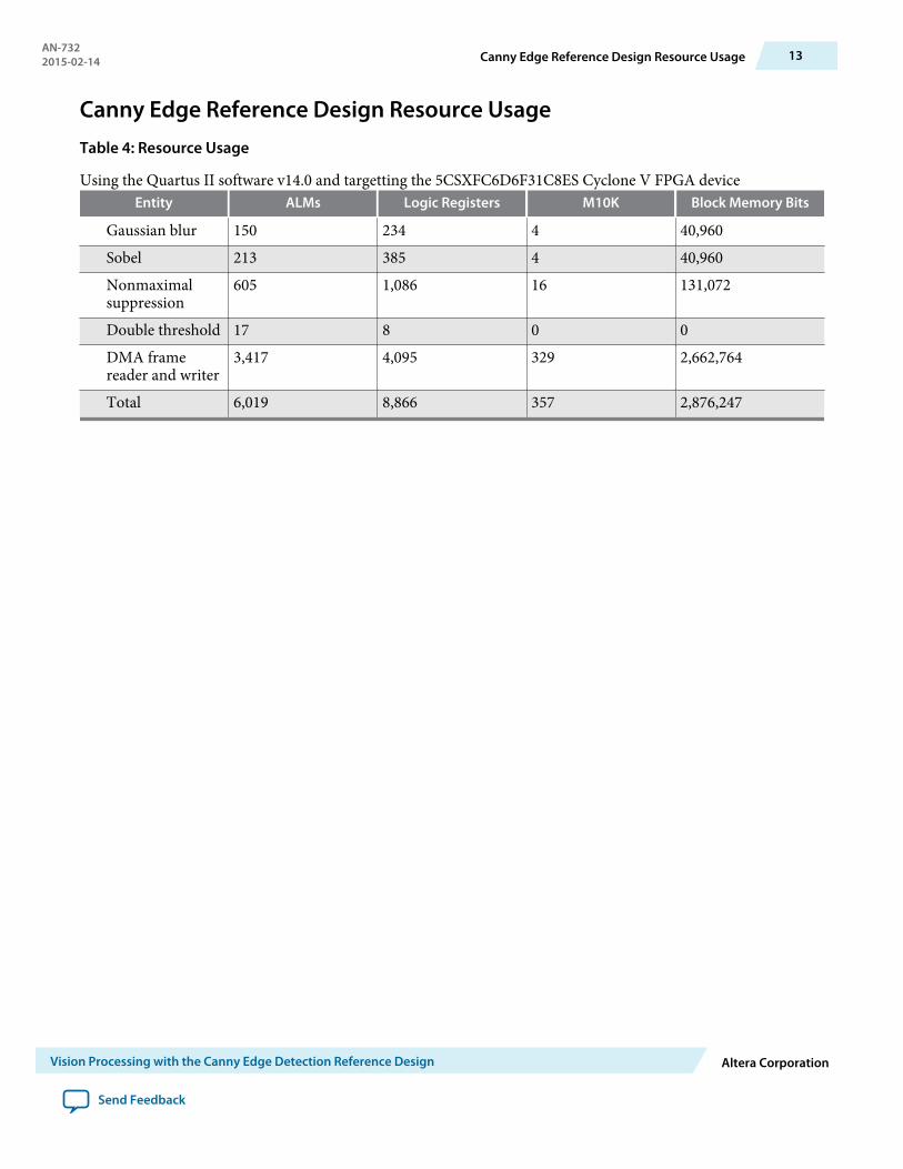
Canny Edge Reference Design Resource UsageTable 4: Resource Usage
Using the Quartus II software v14.0 and targetting the 5CSXFC6D6F31C8ES Cyclone V FPGA deviceEntity ALMs Logic Registers M10K Block Memory Bits
Gaussian blur 150 234 4 40,960Sobel 213 385 4 40,960Nonmaximalsuppression
605 1,086 16 131,072
Double threshold 17 8 0 0DMA framereader and writer
3,417 4,095 329 2,662,764
Total 6,019 8,866 357 2,876,247
AN-7322015-02-14 Canny Edge Reference Design Resource Usage 13
Vision Processing with the Canny Edge Detection Reference Design Altera Corporation
Send Feedback