vlba technical report no. 22 front-end … · interface-device timing 27 ... calibration current...
TRANSCRIPT

VLBA Technical Report No. 22
FRONT-END CONTROL MODULE Module Type F117
Paul Lilie, Lany May and David Weber January 1993

Table of Contents
1.0 INTRODUCTION 1
F117 Physical Description 1 F117 Functional Description 5 F117 Command and Digital Monitor Specifications 6 F117 Analog Monitor Functions 7 Front-End and F117 Analog Monitor Data 7 Front-End Description 7 Front-End Cryogenics Control State Table 8 Front-End Status Codes 10 Front-End Type, Band, Band Codes and Wavelength/Frequency 10
2.0 THEORY OF OPERATION 13
2.1 MONITOR AND CONTROL BUS DESCRIPTION 13
Interface Internal Monitor and Control Functions 15
2.2 STANDARD INTERFACE BOARD DESCRIPTION 19
SIB Functions 19 SIB Interface Signals 21 Execution of a Control Message 24 Execution of a Monitor Data Request for Digital Monitor Data 25 Execution of a Monitor Data Request for Analog Monitor Data 25 Reading the Device ID Code Value 27 Interface-Device Timing 27 Standard Interface Board Power Reset 28
2.3 WIRE-WRAP BOARD CIRCUITRY DESCRIPTION 31
Address Assignments 31 Address Decode Logic 31 Command Registers and Functions 32 Digital Monitor Registers 33 Digital Monitor Data Formats 34 Analog Signal Multiplexing 34 Analog Multiplexer Addresses and Signals 35 Calibration Switching Logic 35 Front-End Calibration Control State Table 36 Calibration Drive Circuitry 36 Calibration Current and Drive Voltage Monitor Circuitry 37 Calibration Drive Inhibit Circuitry 37 Device ID Code Register 38 Power Reset Circuitry 38 Module Serial Number Register Encoding 39 7.5 Volt Reference 39

3.0 BENCH TEST AND AUGNMENT 41
F117 Test Environment 41 F117 Test Fixture 41 F117 Test Program 42 Alignment Adjustments 58
4.0 DRAWINGS 61
5.0 DATA SHEETS 63
6.0 APPENDIX 65
m


List of Illustrations
Figure 1, Photograph of F117 2
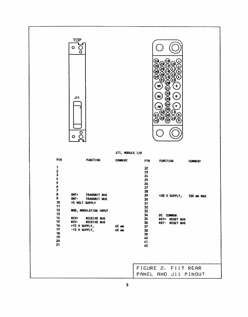
Figure 2, F117 Rear Panel View and Jll Pinout 3
Figure 3, F117 Front Panel View and Jl, J2 Pinouts 4
Figure 4, Monitor and Control Bus Formats 17
Figure 5, Standard Interface Board and Device Logic Block Diagram 23
Figure 6, Standard Interface Board - Device Logic Timing 29
Figure 7, F117 Bench Test Environment 41
Figure 8, SIB EOB Monitor Data, Initial Addresses 47
Figure 9, SIB EOB Monitor Data, Relocated Addresses 50
Figure 10, Successful Test Display 53
Figure 11, Failed Test Display 54
Figure 12, Front-End Monitor Mode Display 55
Figure 13, Typical Backup Display 56
iv

1.0 INTRODUCTION
This manual describes the VLBA F117, Front-End Control Interface module that is used to control and monitor Single-Band, Front-Ends on the VLBA antennas. The emphasis of this manual is on the F117 theory of operation (Section 2) and maintenance (Section 3). Construction details are not included but all drawings used in F117 fabrication are listed in the BOM (Bill of Materials) drawing. Section 4 contains the drawings and Section 5 contains data sheets for the special-purpose components used in F117. Section 6 (the Appendix) lists NRAO reports that describe Single-Band, Front-Ends, the Standard Interface Board and related equipment. The appendix also has a listing of the AOC F117 test program used to bench-test and align the F117.
This manual is an upgrade of an earlier F117 manual and describes the module in more detail. All the tables, drawings, figures, wire list, etc. contained in the first manual have been retained. Additional manual features are a brief description of the VLBA Monitor and Control Bus (MCB), a brief description of the Standard Interface Board (SIB) and the interactions of the Standard Interface Board with the Front-End interface circuitry contained on the Wire-Wrap board. The operation of the Wire-Wrap board circuitry is more fiilly described.
The manual contains several additional drawings. These include the schematic diagram of the Standard Interface Board, the F117 Assembly Drawing, a module wiring schematic diagram, and a more detailed drawing of the Wire-Wrap board circuitry.
A detailed description of the AOC bench tests and test fixture used to align and trouble-shoot the F117 have been included. The AOC bench tests are performed by a test program in an IBM-compatible PC and have been implemented in Microsoft Basic. The F117 test operations performed by the program are described but the details of the program operation are not described. The program is included in the Appendix for readers interested in the program operation.
A brief description of the Single-Band Front-End is included to provide a functional perspective to the the F117 circuitry. The description includes Front-End control logic, command and digital monitor data formats, analog signals and their normal range, and a description of the Front-End supportive environment.
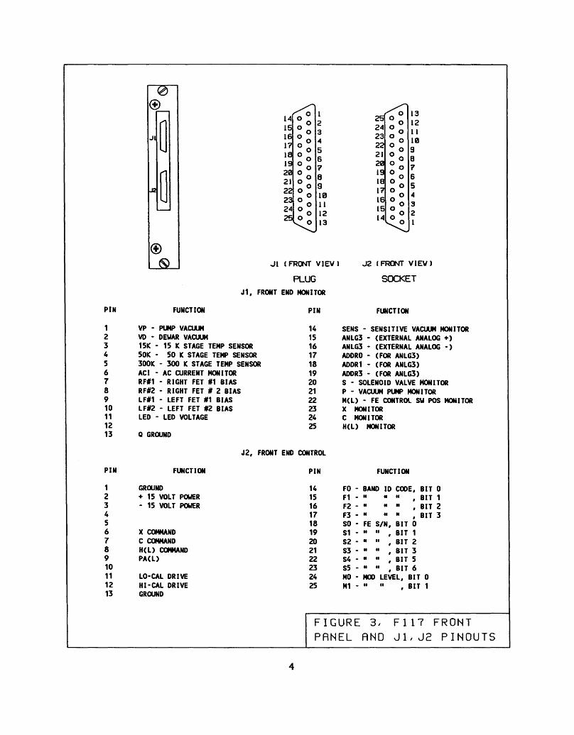
F117 Physical Description
At this point, the reader should refer to drawing D53510A001 (in Section 4) which depicts the F117 Assembly. Figure 1 (next page) is a photograph of the F117 with one side plate removed. The F117 is a 1-wide, RFI-type VLBA module with one 42-pin AMP rear panel connector (PI) that mates with the 42-socket AMP bin connector. Module and Front-End DC power, the Monitor and Control Bus, and the 80 Hz calibration switching signal (MOD) are routed through this connector. Figure 2 (following Figure 1) shows the F117 rear panel and pin-signal assignments. The PI signals are described below.
Two front-panel DB25 connectors (Jl - control and J2 - monitor) interface the F117 to the associated Front-End's corresponding DB25 connectors via two shielded, 25-conductor cables. These connectors carry Front-End DC power, control and monitor signals and three digital status code values from the Front-End that indicate the Front-End's Band Code, Modification Code and Serial Number. The usage of these status codes is described below. Jl (control) is a pin connector and J2 (monitor) is a socket connector. Figure 3 (following Figure 2) shows the front panel and the connector's pin-signal assignments.

FIGURE 1, F117 WITH SIDE PLATE REMOVED
TOP l—D
o O o
J11
1
\om ®^®><®
r?®^N
©s©
iisii
PIN
1 2 3 4 5 6 7 8 9 10 11 12 13 14 15 16 17 18 19 20 21
FUNCTION
XMT* TRANSMIT BUS XMT- TRANSMIT BUS ♦5 VOLT SUPPLY
MOO, MODULATION INPUT
RCV+ RCV- +15 V -15 V
RECEIVE BUS RECEIVE BUS
SUPPLY, SUPPLY,
J11, MODULE I/O
COMMENT PIN
22 23 24 25 26 27 28 29 30 31 32 33 34 35 36
45 inA 37 40 mA 38
39 40 41 42
FUNCTION COMMENT
+28 V SUPPLY, 100 mA MAX
DC COMMON RST+ RESET BUS RST- RESET BUS
FIGURE 2, PRNEL RND
Fl I? REAR Jll PINOUT
PIN
1 2 3 4 5 6 7 8 9 10 11 12 13
PIN
©
Jl
® Jl (FT?ONT VIEVJ J2 (FRONT VIEW)
PLUG SOCKET
Jl, FRONT END MONITOR
FUNCTION
VP - VD - 15K - 50K ■ 300K ACI ■ RF#1 RF#2 LF#1 LF#2 LED •
PUMP VACUUM DEWAR VACUUM 15 K STAGE TEMP SENSOR 50 K STAGE TEMP SENSOR
- 300 K STAGE TEMP SENSOR AC CURRENT MONITOR - RIGHT FET #1 BIAS - RIGHT FET # 2 BIAS - LEFT FET #1 BIAS - LEFT FET #2 BIAS LED VOLTAGE
PIN
14 15 16 17 18 19 20 21 22 23 24 25
Q GROUND
FUNCTION
J2, FRONT END CONTROL
PIN
FUNCTION
SENS - SENSITIVE VACUUM MONITOR ANLG3 - (EXTERNAL ANALOG +) ANLG3 - (EXTERNAL ANALOG -) ADDRO - (FOR ANLG3) ADDR1 - (FOR ANLG3) ADDR3 - (FOR ANLG3) S - SOLENOID VALVE MONITOR P - VACUUM PUMP MONITOR M(L) - FE CONTROL SU POS MONITOR X MONITOR C MONITOR H(L) MONITOR
FUNCTION
1 GROUND 2 + 15 VOLT POWER 3 - 15 VOLT POWER 4 5 6 X COMMAND 7 C COMMAND 8 H(L) COMMAND 9 PA(L) 10 11 LO-CAL DRIVE 12 HI-CAL DRIVE
14 FO - BAND ID CODE, BIT 0 15 Fl - H •• •• f BIT 1 16 F2 - •• •• H f BIT 2 17 F3 - •• •• .. f BIT 3 18 SO - FE S/N, BIT 0 19 SI - " ,, , BIT 1 20 S2 - ,, " , BIT 2 21 S3 - •• " , BIT 3 22 S4 - ■• '• , BIT 5 23 S5 - " " , BIT 6 24 MO - MOO LEVEL, BIT 0
FIGURE 3, F117 FRONT PRNEL RND J1,J2 PINOUTS

The F117 circuitry is contained on two removable circuit boards: the VLBA Standard Interface Board and a Wire-Wrap circuit board which interfaces the Front-End circuitry to the Standard Interface Board.
Since eight PUT'S are currently installed in the antenna vertex room and there is a microcontroller clock oscillator (11.0592 MHz) and digital logic in the F117, the circuitry is contained in an RFI enclosure. Signals and power to the enclosure are fed through feed-through terminals with an integral by-pass filter capacitor. The front panel Front-End interface connectors (Jl and J2) are D-series connectors with integral by-pass filter capacitors on the contacts. RFI gaskets are installed on Jl and J2 to further inhibit RF feedthrough.
F117 Functional Description
Many devices at the VLBA Station are controlled by the VLBA Standard Interface Board (or a functional equivalent) that interfaces devices to die station computer via the VLBA Monitor and Control Bus (MCB). Each controlled or monitored device is tapped onto the bus. The VLBA Standard Interface Board interfaces the MCB signals to the device circuitry. The MCB carries time-serial, digital messages on two multi-drop party-lines consisting of the XMT (Transmit) line and the RCV (Receive) line.
The Standard Interface Board (SIB) in each device analyzes the message stream on the XMT line and if addressed, it executes the designated action. This will be a command to the device or it may evoke data from die device which is serially routed back to the station computer via the RCV line. Section 2.1 briefly describes the Monitor and Control Bus. Section 2.2 briefly describes the Standard Interface Board.
Like many other VLBA Station devices, the F117 contains a Standard Interface Board (version "D") which controls Front-End interface circuitry installed on a Wire-Wrap Board. The interface circuitry consists of logic to interact with the Standard Interface board, command and digital monitor data registers, an analog multiplexer to sample Front-End analog signals, and calibration control and drive circuitry. Section 2.3 describes the operation of the Wire-Wrap board circuitry.
At this point, it is important to review drawing D53510W010 which depicts the F117 internal wiring. This drawing emphasises die signal interconections between the two circuit boards and the Front- End interface connectors Jl and J2.
The Standard Interface Board provides 8 address code bits for address enables, a 16-bit parallel tri-state Command/Monitor (CON/MON) bus for command/monitor argument transfer and interactive hand-shake signals to control the Wire-Wrap board logic. The Standard Interface Board also has an 8- channel differential analog multiplexer/Sample/Hold/A-D Converter to sample and convert the Wire-Wrap board analog signals to digital values.
The Wire-Wrap board contains the following circuitry:
Address decode logic provides enables for two 8-bit command registers (Cryogenics Control and Calibration Control) and enables for four 8-bit and one 16-bit digital monitor registers.
The Cryogenics Command register controls the state of the Front-End cryogenic equipment and the Calibration Control register controls the Front-End calibration circuitry.
The digital monitor registers sample Front-End control logic states and the three Front-End status codes (described below).

Calibration Control logic controls the Calibration Drive circuitry in one of five modes. An externally-supplied switching signal (i.e. Mod, 80 Hz) drives the calibration switching logic. If the noise source drive currents exceed a pre-set level, Calibration Inhibit circuitry inhibits the Calibration Drive.
A 16-channel, single-ended analog multiplexer samples calibration drive voltages and currents and Front-End voltages for conversion by the SIB.
A power-on reset circuit clears the Cryogenics and Calibration Control registers to the zero state when power is applied to the module.1 The cleared state of die Cryogenics control register is interpreted by the Front-End control logic as equivalent to the STRESS state (designated STRESS* in the state table on the next page).
In response to an ID Request signal from the SIB, the Wire-Wrap board asserts a block ID code on the SIB tri-state Command/Monitor bus to identify the Front-End type. The Front-End type code is die Front-End band code.
The F117 has provisions for an external 8-channel analog multiplexer. Jl, the Front-End Monitor Connector, has three address bits and the multiplexer analog output connected to five Jl contacts that are not used in the Front-End circuitry. This external multiplexer is used in module F118 which controls Front-Ends that do not use cryogenic cooling.
The F117 module has an internal RFI-shielded enclosure that contains the SIB and Wire-Wrap board. This enclosure reduces the emissions from die SIB microprocessor clock and digital logic.
F117 functional specifications are tabulated below.
F117 Command and Digital Monitor Specifications
Function Quantity
Cryo Command Word, 8-bits* Cryo Command Echo Digital Monitor, 8-bits*
Cal Switching Command Word, 8-bits** Cat Switching Command Echo Digital Monitor, 8-bits**
RCVR S/N, Band & Mod Codes Digital Monitor, 16-bits RCVR Discretes Monitor, 8-bits*** F117 Serial Number Digital Monitor, 8-bits
F117 Module ID Value, 8-bits (RCVR Band Code)***
Notes: * 3 bits used, 5 spare bits ** 4 bits used, 4 spare bits
6 bits used, 2 spare bits
Mux Address
Mux 20H Mux 20H
Mux 22H Mux 22H
Mux 23H Mux 21H
*** **** see RVCR Band Code values below
1 The Front-End contol logic interprets die cleared state of the Cryogenics Control register as die STRESS mode. STRESS is a test mode which adds an excess heat load to the Front-End to test the refrigerator cooling capacity. If the Front-End is in the computer control mode and a power dropout or glitch occurs, it should be immediately commanded to the COOL state. In normal operation, the Front- End is kept in the (manual) COOL state; this state inhibits computer control of the cryogenics modes.
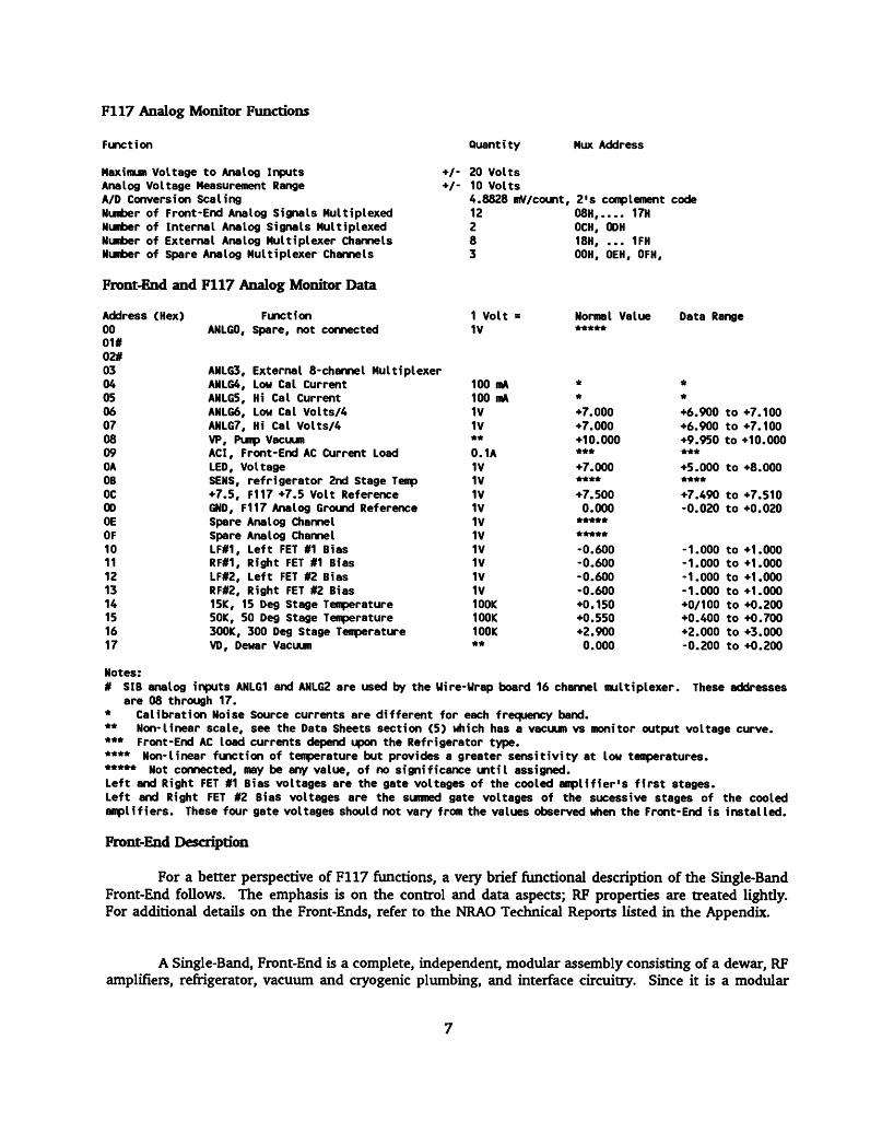
F117 Analog Monitor Functions
Function
Maximum Voltage to Analog Inputs Analog Voltage Measurement Range A/D Conversion Scaling Number of Front-End Analog Signals Multiplexed Number of Internal Analog Signals Multiplexed Number of External Analog Multiplexer Channels Number of Spare Analog Multiplexer Channels
Quantity Mux Address
+/- 20 Volts +/- 10 Volts
4.8828 mV/count, 2's complement code 12 08H,.... 17H 2 OCH, ODH 8 18H, ... 1FH 3 00H, OEH, OFH,
Front-End and F117 Analog Monitor Data
Address (Hex) Function 1 Volt = Normal Value Data Range 00 ANLG0, Spare, not connected IV ***** 01# 02# 03 ANLG3, External 8-channel Multiplexer 04 ANLG4, Low Cal Current 100 mA * * 05 ANLG5, Hi Cal Current 100 mA * * 06 ANLG6, Low Cal Volts/4 IV ♦7.000 +6.900 to +7.100 07 ANLG7, Hi Cal Volts/4 IV +7.000 +6.900 to +7.100 08 VP, Pump Vacuum ** ♦10.000 +9.950 to +10.000 09 ACI, Front-End AC Current Load 0.1A *** *** 0A LED, Voltage IV +7.000 +5.000 to +8.000 0B SENS, refrigerator 2nd Stage Temp IV **** tfttit^t
OC +7.5, F117 +7.5 Volt Reference IV +7.500 +7.490 to +7.510 00 GND, F117 Analog Ground Reference IV 0.000 -0.020 to +0.020 0E Spare Analog Channel IV ***** OF Spare Analog Channel IV ***** 10 LF#1, Left FET #1 Bias IV -0.600 -1.000 to +1.000 11 RF#1, Right FET #1 Bias IV -0.600 -1.000 to +1.000 12 LF#2, Left FET #2 Bias IV -0.600 -1.000 to +1.000 13 RF#2, Right FET #2 Bias IV -0.600 -1.000 to +1.000 14 15K, 15 Deg Stage Temperature 100K +0.150 +0/100 to +0.200 15 50K, 50 Deg Stage Temperature 100K +0.550 +0.400 to +0.700 16 300K, 300 Deg Stage Temperature 100K +2.900 +2.000 to +3.000 17 VD, Dewar Vacuun ** 0.000 -0.200 to +0.200
Notes:
are 08 through 17. * Calibration Noise Source currents are different for each frequency band. ** Non-linear scale, see the Data Sheets section (5) which has a vacuum vs monitor output voltage curve. *** Front-End AC load currents depend upon the Refrigerator type. **** Non-linear function of temperature but provides a greater sensitivity at low temperatures. ***** N0{ connected, may be any value, of no significance until assigned. Left and Right FET #1 Bias voltages are the gate voltages of the cooled amplifier's first stages. Left and Right FET #2 Bias voltages are the summed gate voltages of the sucessive stages of the cooled amplifiers. These four gate voltages should not vary from the values observed when the Front-End is installed.
Front-End Description
For a better perspective of F117 functions, a very brief functional description of the Single-Band Front-End follows. The emphasis is on the control and data aspects; RF properties are treated lightly. For additional details on the Front-Ends, refer to the NRAO Technical Reports listed in the Appendix.
A Single-Band, Front-End is a complete, independent, modular assembly consisting of a dewar, RF amplifiers, refrigerator, vacuum and cryogenic plumbing, and interface circuitry. Since it is a modular
design, differences between Front-Ends are principally in the RF circuitry. This modularity provides greater commonality among Front-Ends which reduces construction costs, eases installation and simplifies maintenance. These Front-Ends may be quickly removed from the antenna for maintenance or replacement without disturbing the other Front-Ends. In removing a Single-Band Front-End, its AC power is disconnected first. Removing the AC power will close the vacuum valve if it was open. The vacuum and cryogenic lines from the manifolds to the Front-End are disconnected next. After completing these simple operations, the Front-End may then be unbolted and replaced by another unit. This simplification of Front-End replacement reduces antenna down-time and the commonality among Front-Ends improves maintainablilty.
A waveguide polarizer on the Front-End input separates the left and right circular polarized (LCP and RCP) signal components for amplification by two cooled amplifiers. Low and High calibration signals are coupled into the Front-End inputs via a power splitter and directional couplers. After passing through the dewar walls, the signals are filtered by band-pass filters and are further amplified by room temperature post-amplifiers. The two signals are then output to die mixers-IF system. An LED in the cooled amplifiers stabilizes HEMT sensitivity. The noise source drive voltage is the same for all Front-Ends but the noise source current may differ between bands. For example, at 20 cm and 3.6 cm (L and X bands), an amplifier is required to achieve the required high noise level. The amplifier is switched by die High cal drive. Only a few few Front-Ends are equipped with a high noise source.
The Front-End is enclosed in an evacuated dewar that is cooled by a closed-cycle. Helium-cooled refrigerator. The dewar is connected to a vacuum manifold through an electrically operated vacuum valve and quick-disconnect coupling. The refrigerator is connected to Helium supply and return manifolds via Arequipt couplings and operates continuously (in die COOL state) but the vacuum pump operates only when commanded by a Front-End. When the vacuum pump is not operating, the vacuum manifold is vented to atmospheric pressure; this helps to seat the Front-End's vacuum valve. The Front-End Helium supply and return pressures should be 270 +/-10 psi and 60 -I-/-15 psi, respectively. Helium supply and return pressures are monitored by F118.
Dewar vacuum, refrigeration and heating control is performed by control logic in the Front-End (described below); control bits X, C and H(L) from the F117 define the five Front-End control states as shown below.2 (A "1" is a TTL high level.)
Front-End Cryogenics Control State Table
H(L)
No refrigerator power, heater power, or vacuum pumping. Normal cooled operation. COOL with small added heat to stress-test cryogenics. Fast warm-up of dewar, 65 Watts of heater power. No refrigerator or heater power.
STRESS* 0 0 0 Reset state of the Cryogenics Control Register
The reason for the all-l's COOL code is that in the event of an "X, C and H(L) stuck high" failure of the Front-End controller or the Front-End J5 cable is disconnected, the control logic defaults to the COOL state, the desired default condition for a Front-End. This state is also convenient for Front-End bench tests. The STRESS command causes a small amount of heat to be generated in the Dewar; die
Control Bit X c Hi
CRYO OFF 1 0 1 C00L 1 1 1 STRESS 1 0 0 HEAT 1 1 0
2 In a sense, the H(L) bit can be considered a "not-heater" bit although it is combined with X and C and temperature-dependent terms in the Front-End control logic. See VLBA Technical Report No. 1 for details.
8
response of the refrigerator to this additional load may be seen in the 15 and 50 degree stage temperatures. The HEAT command is a maintenance command which causes the Dewar to be heated; this permits the dewar to be warming up while Front-End maintenance personnel are on the way to the Antenna. The PUMP command causes the vacuum valve and vacuum pump to be turned on. These states are controlled by Front-End control logic described below.
The STRESS* state is not defined in the Front-End control circuitry. However, when the Cryogenics Control Register is cleared (e.g., a power reset), die Front-End cryogenic control logic reverts to the Stress state3, a refrigerator test state (hence undesirable for sustained periods). When installing an Fl 17 in an antenna with operational Front-Ends or when a power drop-out or glitch occurs, a COOL command should immediately be sent to the PUT'S when power is restored.
Dewar vacuum and temperature transducers are conditioned by a control and monitor electronics card cage attached to the dewar. A mode control switch on die card cage enables the Front-End vacuum, refrigeration and heater circuitry to be set to the CPU control mode or any of the five manual control modes tabulated above: OFF, COOL, STRESS, HEAT, and PUMP. The CPU position permits antenna computer control of these functions via F117 and the Monitor and Control System. In the CPU position, the X, C and H(L) control bits from F117 set the control states to OFF, COOL, STRESS, HEAT or PUMP. When the mode switch is set to any position other than CPU, these functions are determined by X, C and H(L) control bits from die control logic as a function of the mode control switch position. The position of die mode control switch is indicated by the M(L) discrete; if the switch is in the CPU position, M(L) is high ("l11) and it is low CO") in any other (e.g. manual control) postion. In practice, the Front-End control switch is normally set to the COOL state, a manual control condition; therefore, the antenna computer cannot control the cryogenic functions.
Control logic in die card cage controls die operation of the vacuum pump request, vacuum valve, refrigerator, and heater. The control logic inputs are the mode control switch X, C, H(L) and M(L) bits; the F117 X, C and H(L) control bits; dewar (VD) and port (VP, manifold) vacuum; dewar (15K, 15 deg stage) temperature and AC current load (ACI). Control outputs are the discretes: vacuum valve solenoid drive S, pump request P, refrigerator motor power and dewar heater power. The operations performed by the control logic are described in the next paragraph.
Vacuum valve operation is inhibited if die pump port (VP, manifold) vacuum is above 50 microns. The vacuum valve is opened if the pump port vacuum is less than the dewar vacuum (VD) and the dewar vacuum is greater than 7 microns. The discrete signal S indicates the state of the vacuum valve command. The pump request signal (P) becomes true (i.e., a "1") if dewar vacuum exceeds 5 microns and goes false ("0") if the dewar vacuum becomes less than 3 microns. The discrete monitor signal P indicates the state of the pump request signal. The refrigerator operation is inhibited if the dewar vacuum is above 50 microns. The Front-End control logic is designed to continue the refrigerator operation in the event that the J5 cable (power and control bits) from F117 is disconnected. This permits maintenance of the system electronics but does not affect die cryogenics operation. The control logic turns on the heater when the mode switch is set to HEAT or when the central computer commands die HEAT state. The control logic also protects the dewar from overheating by the heater when in the HEAT state.
Monitor circuitry in the card cage reads out the three operative control bits (X, C and H(L) from either F117 or the mode control switch (depending upon the switch position), M(L) (the mode control switch status) and control output discretes P and S. The monitor circuitry also reads out the following analog values: vacuum (VD, dewar and VP, pump port); linear temperature measurements (15K, 50K and 300K degree stages); a non-linear temperature measurement (SENS, on the 15 degree stage); AC current
VLBA Technical Report No. 10

load (ACI); HEMT and FET gate bias levels (LF#1, LF#2, RF#1, RF#2), and the LED voltage. These parameters are output to F117 analog multiplexers via monitor connector J2. The normal values and working range are tabulated above.
A 12-position manual selector switch and integral DMM on die card cage permit the analog parameters to be monitored locally.
Front-End Status Codes
The Front-Ends read out digital status code values that indicate die Front-End frequency (Band Code), Front-End Serial Number, and the Modification Level These codes are hard-wired in the Front- End when it is manufactured and are output to the F117 on die Power-Control-ID connector J2. These codes are:
The Band Code is a four-bit binary plus parity (even) code (bits F0 through F3 and PA, parity), from the Front-End via die J2 (monitor) connector.
The Front-End type, WL (wavelength in cm or mm), freq (frequency, MHz or GHz) and Band Code (Hex) are tabulated below.
Front-End Type, Band, Band Codes and Wavelength/Frequency
FE Type Band UL/Freq Code
FE Type Band UL/Freq Code
F101* P 00H 400 cm/75 MHZ F102 P 01H 90 & 500 cm/330 & 610 MHz
F103 L 02H 20 cm/1.4 GHz F104 S 03H 13 cm/2.3 GHz
F105 C 04H 6 cm/4.8 GHz F106 X 05H 4 cm/8.4 GHz
F107* X 06H 2.8 cm/10.7 GHz F108 U 07H 2 cm/15 GHz
F109 K 08H 1.3 cm/23 GHz F110 Q 09H 7 inm/43 GHz
* Not currendy implemented on the VLBA
Front-End Serial Number is a six-bit binary hard-wired code (bits S0 through S5) from the Front- End and is unique to each Front-End. Front-End Serial Number ranges from 1 through 63.
The Modification Code is a two-bit code (M0 and M,,) that indicates the Front-End modification level.
Two DB25 connectors on the Front-End provide the +/- 15V Front-End Power and the F117 control and monitor connections. Two shielded, 25 conductor cables connect an F117 to a Front-End. J5 (25 pin contacts) carries Front-End Power, the antenna control computer X, C and H(L) control bits, the Band Code code bits, the Front-End Serial Number code bits and Front-End Modification Level bits. 32 (25 socket contacts) carries analog and discrete monitor signals. Figure 3 shows the assignments of these power, control, status codes and monitor signals on the F117 front panel Jl and 32 connectors.
A dedicated (for each Front-End) Refrigerator Drive Unit (Pill for 5 GHz through 43 GHz Front- Ends or PI 12 for 1.5 GHz through 2.3 GHz Front-Ends) in the Antenna Vertex Room Feed Tower provides
10

two-phase, 150 Volts AC power for the Front-End. The refrigerator Drive Unit has an isolation transformer and phase shift network to generate the shifted phase. The unshifted phase of this 150 volt AC also powers the vacuum valves and dewar heaters. Pill (or PI 12) also has an AC current transducer to measure the Front-End total AC current load. This Front-End AC current load is monitored by F117 multiplexer channel 09H.
The Helium Supply and Return Pressure and vacuum pump functions are common to cooled Front-Ends. Two Helium compressors typically drive five Front-Ends; F118 monitors the output of the four pressure transducers used to monitor the two compressors' Helium supply and return manifolds. Each F117 monitors its associated Front-End's Dewer and Pump vacuum.
A-Rack power supplies provide the Front-End's +15 and -15 DC Power via F117. The B-Rack +/- 15, +5 and +28 Volt DC power is monitored by F118.
In addition to the two DB25 connectors mentioned above, the Front-End has an "AUX" DE9 (9 socket contacts) 34 connector which carries the Pump Request (P) and a return. This signal is combined with eight other Pump Requests in the Vacuum Pump Controller installed in the "A" Rack. This unit functions as an eight-input OR gate; when any Front-End Pump Request becomes true (high), the controller logic turns on a solid state relay to apply AC power to the Vacuum Pump.
When an F117 is removed from the bin or the PUT'S 32 cable is disconnected, the associated Front-End cannot activate the Vacuum Pump Controller.
The Single-Band, Front-Ends do not have an internal transfer switch to interchange the LCP and RCP signals for test purposes. This feature is implemented in die Converter Modules (TlOl through T110).
11

12
2.0 THEORY OF OPERATION
The VLBA Monitor and Control Bus (MCB) is described in Section 2.1. The Standard Interface Board interacts with the MCB and activates the Wire-Wrap board circuitry. It is described in Section 2.2. These two descriptions provide the basis for the description of the Wire-Wrap board circuitry in Section 2.3.
2.1 MONITOR AND CONTROL BUS DESCRIPTION
This MCB description is abstracted from VLBA Technical Report No. 12. Some details of the bus description have been omitted for brevity; these details are factors in the design of the SIB and are not a concern of this manual. Readers interested in a more detailed description of the MCB are referred to this Technical Report.
In the bus and SIB descriptions below, the term "Device" refers to a unit (module, etc.) containing a Standard Interface board or a functional equivalent. F117 is a typical device.
The VLBA Monitor and Control Bus (XMT and RCV) conform to the EIA RS-485 signal specification.
Interface Address Block
Each Device Interface (Standard Interface Board) is assigned a unique block of contiguous addresses to which it alone responds. The block may be any length up to 256 addresses and is disjoint with the address blocks of all other Interfaces. The last 16 addresses (described below) of each block are dedicated to storage of the ID byte value N, block start address and error counters (parity, etc.) internal to the Interface. These counters may be read out as monitor data.
The MCB consists of two differential-mode logic signals, each on a shielded twisted pair cable wired as a multi-drop party line. The bus signals are called Transmit Data (XMT) and Receive Data (RCV). The MCB Controller is the station computer which transmits messages on the XMT line and receives messages on the RCV line. The Interfaces (one at a time) are the sources of Receive Data. Data is bit-serial at a rate of 57.6 kbaud and die transmissions are byte asynchronous. Each byte consists of, in order, a start bit (binary 0), eight data bits fleast significant bit first), one parity bit, and one stop bit (binary 1).
XMT and RCV bus messages are combinations of data value bytes and control function codes. The data value bytes are address and argument values: Address High (ADH), Address Low (ADL), Control Data High (CDH), Control Data Low (CDL), Monitor Out High (MOH) and Monitor Out Low (MOL). Data value bytes are transmitted with odd parity.
Control function codes (bytes) signal the start of a message or report interface-device status during the execution of control and data request messages. The Control Function codes are: Synchronization (SYN), Acknowledge (ACK), Second Acknowledge (DC1), Non-Response Acknowledge (DC2) and Negative Acknowledge (NAK). Control Function codes are transmitted with even parity.
XMT Line
Every message on the XMT line is exactly five bytes long and the bytes occur in the following sequence: SYN, Address High (ADH), Address Low (ADL), Control Data High (CDH) and Control Data Low (CDL). The SYN byte indicates the beginning of a message and is the only even bit parity byte on the XMT line (thus distinguishing it from all data bytes). The SYN byte is followed by ADH. If the most
13
significant bit of ADH is 1, then the message is a control message; otherwise it is a monitor request message. The remaining 15 bits of ADH/ADL form a binary address in the range of 0 through 32767.
Each Standard Interface receives ADH and ADL of every message on the XMT line and compares it with its assigned address block. If the address is within the assigned interface address block and there is no parity error, then shortly after (<382 usee) the last bit (Stop) of ADL, the interface must begin to transmit a one byte acknowledge code (ACK) on the RCV line.
A DC1 second acknowledge code is transmitted on die RCV line if the following conditions are met: SYN, ADH, ADL, CDH and CDL have valid parity, the address is within the assigned block, a control message is specified (indicated by a 1 in the msb of the ADH) and the device responds to the interface handshaking properly.
The Interface checks parity on all bytes received. If SYN has a parity error, an internal counter is incremented.
If ADH or ADL has a parity error, the Interface does not respond (just as if die address were outside its block), but increments an internal address parity error counter and looks for the next valid SYN.
A negative second acknowledge code NAK is transmitted on die RCV line if: SYN, ADH and ADL have valid parity, the address is within the assigned block and a control message is specified, but CDH or CDL has a parity error. In this case CDH/CDL is not passed to the device and a control data parity error counter is incremented.
A second form of negative acknowledge byte (DC2) is returned if the interface is unable to complete its handshaking with the device to which it interfaces. The device non-response condition is counted by two internal counters (one for commands and one for monitor data).
If the message is a monitor request message within the address space assigned to monitor data, the CDH and CDL byte values are ignored; they have no meaning. The parity of CDH/CDL is, however, tested and the control data parity error counter is incremented if tainted by an error. In this case, the monitor data specified by ADH/ADL is returned in the normal manner because the CDH/CDL parity error has no effect upon the validity of the monitor data.
RCV Line
Messages on the RCV line are either a two byte command acknowledgement or a two or three byte monitor data acknowledgement, as follows:
Command acknowledgement messages are: 1) ACK, DC1 (normal, no fault command execution acknowledgement), 2) ACK, NAK (CDH/CDL parity error acknowledgement), and 3) ACK, DC2 (device non-response acknowledgement).
Monitor request acknowledgement messages are: 1) ACK, MOH, MOL (normal, no fault acknowledgement followed by two bytes of monitor data obtained from the address specified by ADH/ADL); 2) ACK, DC2 (fault acknowledgement, monitor data is unavailable from the device).
The Controller also checks parity on all bytes received on the RCV line. In the event that monitor data or function codes have parity errors, the Controller application software notes the errors and disqualifies the data.
14
Bus Timing
The first acknowledge byte (ACK) also functions as a clear to send to the controller, granting the controller the right to begin its next message, and promising to yield the RCV line before it is needed for another interface's response. The interface will have at least 573 microseconds after the end of transmission of CDL to disconnect from RCV.
The Controller may begin transmitting another message following a control message after the receipt of the acknowledge (ACK) byte. Figure 4 (following this section) shows the XMT and RCV bus formats and maximum-speed and minimum-speed timing for sequences of control messages and monitor requests.
Note from Figure 4 that in the maximum rate mode of control message reception, the interface is transmitting the second acknowledgement (DO) concurrent with the reception of a new control message.
Note also from Figure 4 that in the maximum rate mode of monitor request message reception, MOH/MOL are being transmitted on RCV at the same time that a new message is being received on the XMT bus.
Function Codes
The hexadecimal byte values for the control function codes are as shown below. These bytes are transmitted in even parity, which makes diem unique since data bytes are odd parity.
SYN - 16, Synchronization byte which prefixes all messages from the controller.
ACK - 06, First acknowledgement byte to the controller which signifies that SYN was detected and that SYN, ADH and ADL did not have parity errors. ACK is not transmitted if there was a parity error on any of these three bytes.
DC1 - 11, Second acknowledgement byte to the controller which signifies that in die case of control messages, there were no parity errors in CDH/CDL and the device responded properly to the interface-device handshaking requirements.
NAK - 15, Negative acknowledgement byte to the controller which signifies that, for control messages, CDH/CDL was tainted by a parity error.
DC2 - 12, Second negative acknowledgement byte to the controller which signifies that the device logic did not respond to the interface handshaking within the allocated time period. This non- response acknowledgement is used for both control and monitor request messages.
Interface Internal Monitor and Control Functions
The last 16 addresses in the address block are allocated to Monitor and Control parameters internal to the Standard Interface board. The occurrence of bus fault conditions (such as parity errors, invalid SYNC, etc.) is accumulated in counters and is available for monitor data readout by the Controller. Device non-response events are also accumulated. These parameters were described above. The counters are capable of being reset or set to other values by a control message from the Controller.
Other parameters in this block are the Interface Type and Revision level, Block ID Code (N) and Address Block start address. This Block ID Code is the index for assignment of the address block by the
15

Controller. None of these locations (indicated by bold print) can be overwritten by the Controller. The last three addresses in the block are reserved for future assignment.
These Interface addresses are identified by the notation: BE-1, BE-2, etc. where BE designates the Block End (last) address. The assignments are as follows:
Address Value
BE-15 Reserved for future use BE-14 M " •• M
BE-13 M MM*
BE-12 No Control Response counter (i.e, no DEV ACK from device) BE-11 No Monitor Response counter (i.e., no DEV ACK or ANENB from device) BE-10 Interface Type and revision code (cannot be altered fay the Controller) BE-9 Address of last control message received, (i.e., ADH and ADL) BE-8 Control data for last control message received, (i.e., CDH and CDL) BE-7 Address parity error counter, all messages BE-6 Control data parity error counter, all messages BE-5 Invalid SYN character BE-4 Control data parity error counter, messages in block BE-3 N, ID byte value from device logic (cannot be altered by the Controller) BE-2 Count of correctly received control messages BE-1 Count of correctly received monitor data request messages BE-0 Address of beginning of block (cannot be altered fay the Controller)
16

XMT
K 95S US H ^H 191 US h*-
SYN RDH RDL CDH CDL SYN RDH RDL CDH CDL
RCV RCK DC1 RCK
MRXIMUM RRTE CONTROL MESSRGE TRRNSMISSION
XMT SYN RDH RDL CDH CDL SYN ADH RDL CDH CDL
h- <382 US <573 US
RCV RCK MOH MOL
MRXIMUM RRTE DRTR REQUEST MESSAGE TRANSMISSION
<11H6 US
XMT SYN RDH RDL CDH CDL SYN RDH RDL CDH CDL
K ose us <573 US H
RCV RCK DC1
MINIMUM RRTE CONTROL MESSRGE TRRNSMISSION
XMT SYN RDH RDL CDH CDL SYN RDH RDL CDH CDL
K <382 US » < <382 US H RCV RCK MOH MOL
MINIMUM RRTE DRTR REQUEST MESSAGE TRRNSMISSION
FIG 4, XMT RND RCV BUS TIMING
17

18
2.2 STANDARD INTERFACE BOARD DESCRIPTION
This section describes the VLBA Standard Interface Board, Version "D" (for differential analog signals). The previous section described the MCB bus and the bus-SIB interaction protocols. This section briefly describes the operation of the Standard Interface Board and its interactions with the Wire-Wrap board circuitry.
The material in this Section is an adapted abstract from VLBA Technical Report No. 12. The Wire- Wrap board circuitry is fiilly described in Section 2.3.
This section does not describe the SIB microcontroller and support chips, the microcontroller firmware and the A/D Converter. Readers interested in a more detailed description of die Standard Interface Board are referred to the Technical Report cited above.
The description is based upon die assumption that XMT line messages are error-free. In the event of a parity error, the SIB performs the operations outlined in Section 2.1 above.
SIB Functions
The Standard Interface Board (version "D") logic schematic is shown on drawing 0550025002. The reader should frequently refer to this schematic during the following description.
An Intel 8032 Microcontroller is the logic element that receives and analyzes the XMT bus messages and outputs die RCV bus messages. The 8032 firmware program execution controls all operations of the SIB with the exception of the SIB power reset. The 8032-driven SIB circuits activate die Wire-Wrap board logic to store command argument values in the designated registers and gather and format designated digital and analog monitor data from the Wire-Wrap board circuitry for output on the RCV line.
Following the successful (i.e., error-free) reception of a control or data request message, the SIB will have stored 16-bit ADH-ADL and CDH-CDL values.
The lower 15 bits of ADH-ADL is the address of some device function such as a command register or monitor data source. When the MSB of ADH is a "1", the message is a command message and when it is a "0", it is a Data Request message. The SIB block start address is subtracted from the ADH-ADL value to form an 8-bit Relative Address which is parallel-output to the Wire-Wrap board on die RAO, ... RA7 lines. The Wire-Wrap board uses only six of these addresses which are designated ADDRO,... ADDR5 in the schematic diagrams. Decode logic in the Wire-Wrap board generates enable terms to store command arguments in the two command registers or to read monitor data to be read from digital registers.
The 16-bit CDH-CDL value is the control message argument to be stored in the address designated by ADH and ADL. These 16 bit values are asserted upon the SIB parallel tri-state CON/MON bus. The Wire-Wrap board stores the CON/MON argument in the register designated by the ADDRO, ... ADDR5 state using the SIB handshake signals (described below). CDH and CDL values have no meaning if the message is a Data Request.
Because analog signal multiplexing and A/D conversion are frequently required, the Standard Interface Board contains an analog multiplexer-A/D Converter. The converter is integrated into the logic of the interface so that it may be easily applied to analog signal monitoring applications. The analog mulitplexing capacity of the interface may be extended by additional analog multiplexers installed in the
19

device circuitry. On drawing D55001S002, note that the 12 A/D converter data bits are connected to the upper 12 CON/MON bus lines; the lower 4 four bus lines float, which makes them indeterminate.
The A/D Converter output is a 12-bit, 2,s complement code with a resolution of 4.8828 mV/count. The 12 data bits are left-adjusted in the 16-bit data value and the four lower buts are undefined. The 16- bit formats of plus full scale, minus full scale and center scale values are tabulated below.
Value, Volts MSB LSB +9.995 011111111111UUUU
I i I
! ! ! +0.005 000000000001UUUU 0.000 oooooooooooouuuu -0.005 111111111111UUUU
I I I -9.995 100000000001UUUU
-10.000 1 ooooooooooouuuu
U Denotes undefined states.
To convert the analog data values to volts, truncate the 16-bit value to 12 bits by a fixed-point divide by 16 or a four-bit right shift and multiply the resultant (2's complement) value by 0.0048828. Dividing by 16 eliminates the four least significant bits which are undefined.
The use of HI/LO SEL logic makes the analog signal address space compact when device multiplexers are used in conjunction with the on-board analog multiplexer. This is accomplished by device address decode logic to control the state of HI/LO SEL as described below. If HI/LO SEL is low, address bits RAO, RA1 and RA2 select the on-board analog multiplexer channel and if it is high, RA5, RA4 and RA5 control the channel selection.
If no more than eight analog signals are to be multiplexed and converted to digital values, HI/LO SEL should always be low. In selecting an input signal, the on-board address multiplexer is controlled by the three lowest bits of RA: RAO, RA1 and RA2.
If the device circuitry has analog multiplexers, their outputs are connected to the inputs of the board multiplexers, ANLG-0 .... ANLG-7. RA bits RAO, RA1 and RA2 control die channel selection in these device multiplexers.
The SIB address bit multiplexer is a quad two-to-one (74LS157) multiplexer with RAO, RA1 and RA2 connected to the A inputs. The next three address bits (RA3, RA4 and RA5) are connected to the B inputs. A low on the SEL line will select the A inputs and a high will select die B inputs. The three outputs of the 74LS157 are connected to the address inputs of the SDM-854 multiplexer-S/H-A/D Converter.
Note that in the table of F117 Analog signals shown above (Section 1), some analog signals are connected directly to SIB analog inputs (e.g., ANLG4,.. ANLG7) and others are connected to multiplexers whose outputs drive ANLG1-ANLG2 and ANLG3. Note that the analog addresses are a contiguous block. Logic in die Wire-Wrap board controls the SIB address multiplexer via the HI/LO SEL line. The implementation is described in Section 2.3.
By implementing HI/LO SEL logic similar to that used on the Wire-Wrap board, up to 64 analog signals can be multiplexed using a combination of device multiplexers and the SIB multiplexer inputs with a contiguous address space.
20

SIB Interface Signals
The following signals interface the SIB to the Wire-Wrap board circuitry:
RA Relative Address is the difference between the 16-bit bus address (ADH-ADL) and the first address of the block. RA is 8 bits which provides 256 addresses. The F117 Wire List and Wire-Wrap board logic schematics use the notation ADDRO (LSB), ADDR1, ADDR5 to designate these address terms.
CON/MON CON/MON is a 16-line, parallel tri-state bus used for message argument interchange between the SIB and Wire-Wrap board logic. During the intervals between argument transfers, the SIB tri-state drivers are disconnected. Wire-Wrap board logic connected to the CON/MON bus is also disconnected from the CON/MON bus after an argument transfer. The F117 Module Wire List, the Wire-Wrap board schematic diagrams and the module wiring diagram all use the notation C/M 0,.... C/M 15 to designate these bus lines.
R/W- R/W- (read/write-not) designates the type of interaction with the device logic. If low, it requires the Wire-Wrap board to read the data standing on the CON/MON bus. If high, it requires the Wire-Wrap board (or the SIB A/D converter) to assert monitor data on the CON/MON bus. R/W- is held low during die interval between message executions. This signal is designated R/W(L) in the F117 Module Wire List and Wire-Wrap Board logic schematics.
DEV ACK read
ANENB
DEV REQ DEV REQ (Device Request) signals the Wire-Wrap board that a command or monitor operation must be performed. The Wire-Wrap board decodes the RA and executes the control or monitor data action as a function of the address. DEV REQ remains high until the Wire-Wrap board returns a DEV ACK (Device Acknowledge) or an ANENB (Analog Enable) signal which will cause DEV REQ to go low. In the event the Wire-Wrap board logic does not return a DEV ACK (or ANENB) signal within 500 usee, the SIB disconnects the CON/MON bus, drops DEV REQ and signals a no-response fault to the controller by outputting a DC2 function code on the RCV line.
DEV ACK (Device Acknowledge) signals that the Wire-Wrap board has (if a command) the command argument on die CON/MON lines or (if the requested data is digital) has asserted the requested data upon the CON/MON bus.
ANENB (Analog Enable) is the DEV ACK counterpart when RA specifies an analog signal. ANENB signals the SIB that RA specifies an analog signal which is to be sampled and converted by the SIB analog multiplexer and A/D converter. ANENB is generated by the Wire-Wrap board address decode logic. When ANENB goes true, the analog multiplexer selects the RA-designated channel and the A/D conversion process is initiated. In this A/D conversion to case, the Wire-Wrap board logic holds DEV ACK low. If RA does not specify an analog address, the Wire-Wrap board logic holds ANENB low.
HI/LO SEL HI/LO SEL signals the SIB that either the lower three RA bits (RA:0,1,2) or the next three RA bits (RA:3,4,5) are to be used by the on-board analog multiplexer. HI/LO SEL controls this multiplexer. HI/LO SEL should always be low if only the SIB analog multiplexer is used. If both the on-board and device multiplexers are used in conjunction, (as is the case in F117), HI/LO SEL should be set high if the RA specificies an address for an external multiplexer whose output is connected to one of the SIB analog multiplexer inputs. Proper usage of the HI/LO SEL term enables remote analog multiplexers and SIB
21
analog multiplexer addresses to be contiguous in address space. (See the HI/LO SEL logic description in Section 2.3 below.)
ANLG-X ANLG-X are eight sets of differential analog signal inputs which are to be selected and converted to digital values for monitor data readout.
ID REQ ID REQ is 8032 port P1.5. When ID REQ goes low, the Wire-Wrap board logic asserts the Block ID code on the CON/MON bus as described below.
At this point, the reader should refer to the Standard Interface Block Diagram (Figure 5) on the next page to put these bus and device interface signals into context.
22
t —r- I lA in
_l
a a u 2 " s g
a:
Z (J S a
o- 1 m JL i- •-■ 0£ •-• _
" s U> 2 5 °A7 1 "* = O 2 O 5 0 Q 0
1 = <1 o a Ul -i
■ 1 O _l O 2 -■ o _l
u o Q -•
z , L I J -1 t
1 "* ^ 2 u Ul CD
a DC
c ft J a Hi 1 1 ■el a L_ 1 z o _ _ _ T _ _ _ o > > 3 IU -1 u
Ul Ul v r N. a a K a t^ a ;—
r u i i Z \
1 f " ' 3 • a
> w
1 o ua c OM
1 v. i Q
1 c ■ u a
?f a o
cc _i o o
a i-
a 1 ■ -J z o
a z <
w iu o 3 > u
1 a a
a o u X ■ ' - in
1 i I a -1 > ■ z a. 0) « 3
c CD 1 X -i (T 2
1 ' r Z 111 M
c > ea a o o
-I
z
U O
I c" o a. a. 0 v o o.
3 8 T £ S r; n o * = 00 a; Q.
£ 0£ <
OC CO i * IE
1 s h z z <E yc •_ P « u (C 2« •-' •-•- 3
<E3 C OO
1 X ■=>
E 3
I CA
3 CD
« i X 3 C
a
X 00 a
= a a. as , ac 13 Ul ^
a u. u
o »- S s C9 0) "
S A « i ^ 111 / \ l-O o
a a
X o _l " ae - | * I-
3 - 1 a a
c a 111 O CL OB- ii _l
" " "T S • S s Is
1 » K Q. 3
s o o u u
»- o s 0
_ o u u
<D
N s S * «) r a a
1
3 i r
at
1 w
! a a: a>
Ul at
Ul OC
_
1 C o 1_ a
• CD
1 Q 1 c
IK a o a:
ftl ^ »
i.5 1- CJ
>- ^ Ul
Q E m ui J ui •-• - 1 ^ z ■S E (/)
L
r ui a ce _i A I- w 3 1-
CQ CO 1
ao. x — x «» •- a. at a. 1
! ,i ♦ ♦ «. 1 1 ! ■» T \ / ! '^ 1 \ Z^J •.. n \/^ A 1 -* U Y /\ 1 -E "—' ' / \ • 1 / \ 1-
a. o a: •-• a o z o a: _i »- V) UJ
u ec •-• m >
3 a: •-• o
23

Referring to the SIB Schematic Diagram D55002S002, the reader will note that the SIB interface stimulus logic signals listed above are derived from four control discretes from Port B of 132, an Intel 8755. These glitch-free bits, BFR ENABLE, CMD RLSE, R/W- and IOR are set and cleared by the firmware during the course of interactions with the Wire-Wrap board logic. During the following discussion, the reader should refer to the SIB schematic diagram to see how these control discretes are used.
The SIB performs five types of operations, four of which are controlled by the microcontroller. After the hardware power-up reset and firmware initialization of hardware, the board operations are a response to the XMT bus signals described in Section 2.1.
The four firmware-controlled operations are: 1) Execution of a control message command to die device, 2) Acquisition of digital monitor data from the device in response to a monitor data request message, 3) Acquisition of analog monitor data from die device in response to a monitor data request message, 4) Device ID code read. These are described in this order below.
The descriptions below assume that there are no XMT line parity errors. In responding to all three types of messages, the SIB outputs an ACK to the Controller < 382 uSec after the reception of the ADH and ADL.
Execution of a Control Message
When a control message is received with an address within the assigned F117 address block, the firmware writes the eight bits of Relative Address (RA) into Port A of the 8755. RA is immediately available to the Wire-Wrap board address decode logic and precedes DEV REQ by about 24 uSec. RA remains static until changed by another message execution.
The message ADH byte MSB is a 1; this designates a control message so the firmware sets the 8156 Ports A and B to the output mode and writes the command argument into these Ports. The R/W- line is (normally) low which signals the Wire-Wrap board logic that an RA-designated command register is to be loaded. R/W- also sets the 74LS245 CON/MON Bus driver's direction to output (from the SIB) mode. At the same time that R/W- is set low, the command argument is asserted on the CON/MON Bus. These operations are completed several uSec before DEV REQ goes true (high).
DEV REQ is set high (true) which enables the Wire-Wrap board address decoder. The Wire-Wrap board responds to the DEV REQ signal with a DEV ACK signal after (about) a 20 nSec delay. After a firmware delay of several microseconds, the SIB lowers the DEV REQ signal and disconnects the 8156 Ports from the CON/MON bus. Lowering DEV REQ disables the address decoder. The trailing edge of die RA-designated decoder enable output docks the lower eight bits of the argument on the CON/MON bus into the selected command register. About 20 nSec after DEV REQ goes low, the Wire-Wrap board lowers the DEV ACK line which completes die SIB-Wire-Wrap board command transfer.
The SIB then outputs a DC1 function code to the Controller via the RCV line to signify the completion of a control message execution.
In the event of a malfunction in the Wire-Wrap board logic that would inhibit the DEV ACK response, the firmware has a 500 usee timer which causes a DC2 (no F117 response) function code to be output to the Controller via the RCV line. In this case, the SIB lowers the DEV REQ signal.
After completion of the command, the R/W- line stays low and RA remains static until the next message execution.
24

Execution of a Monitor Data Request for Digital Monitor Data
When a monitor request message is received with the address within the assigned F117 address block, the firmware writes the eight bits of Relative Address (RA) into Port A of the 8755. RA is immediately available to the device address decode logic and precedes DEV REQ by about 18 uSec. RA remains static until changed by another message execution.
The following description assumes that RA specifies a digital monitor data register.
The message ADH MSB will be 0; this identifies a monitor data request. Consequendy the R/W- control discrete is set high. The high state of R/W- conditions the Wire-Wrap board address decode logic to generate monitor data enables for the output of Digital Monitor data to the SIB on the CMD/MON bus. Since R/W- is high, the 74LS245 CON/MON bus drivers are set to the input (to the SIB) direction; this steers data from the device to die 8156 Ports A and B via die bus.
8156 Ports A and B are set to the input mode by die firmware.
The SIB sets DEV REQ high (true) 18 uSec after R/W- is set high. DEV REQ enables the Wire- Wrap board address decoder; the RA-designated decoder enable output holds the selected monitor data register static and causes the register outputs to be asserted onto the lower eight bits of die CON/MON bus.
The Wire-Wrap board responds to the DEV REQ signal with a DEV ACK signal after (about) a 20 nSec delay. This loads the data into the 8156 Ports A and B via the CON/MON bus. After a few uSec of firmware delay, the SIB responds to DEV ACK by reading die digital monitor data in the 8156 Ports A and B. The SIB then lowers the DEV REQ signal. When DEV REQ is lowered, the Wire-Wrap board lowers DEV ACK after about a 20 nSec delay.
After lowering DEV REQ, the SIB outputs the MDH and MDL monitor data to the Controller via the RCV line; this completes the monitor data request message sequence.
In the event that DEV ACK does not go true within 500 usee after DEV REQ has gone true, a firmware timer causes the DC2 function code to be output to the Controller on the RCV line; DEV REQ is also lowered.
Because the requested data is digital, the Wire-Wrap board address decode logic holds the ANENB line low. The HI/LO SEL line is a "don't care" case; the state of this signal does not affect the digital monitor data gathering sequence.
After the monitor data has been output to the Controller, the R/W- line reverts to the low state. RA will stay at die current message value until changed by die next message within the address block.
Execution of a Monitor Data Request for Analog Monitor Data
When a monitor request message for analog data is received with an address within the assigned address block, the firmware writes the eight bits of Relative Address (RA) into Port A of the 8755. RA is immediately available to the device address decode logic. RA remains static until changed by another message execution.
Although there are significant differences between the circuitry for digital and analog monitor data operations, both use the same 8032 firmware; the board logic makes both operations seem identical to the firmware.
25

The message ADH MSB is 0; this identifies a monitor data request and causes R/W- to be set high. The Wire-Wrap board logic does not use R/W- in executing a data request message for analog data.
The first steps in the execution of a request for analog data are similar to that for gathering digital monitor data.
8156 Ports A and B are set to the input mode and the CON/MON bus direction is set to input data to the 8156 Ports A and B.
The device must decode RA to determine whether the monitor data request is for digital or analog data. If analog data is specified by RA, the logic operations are quite different than for die digital data case. Instead of reading device registers on the CON/MON bus as in the digital data input case above, analog multiplexers on the board and in the Wire-Wrap board select the analog signal designated by RA. The selected analog signal is sampled by the SIB A/D converter sample-and-hold circuit and converted to a digital value. The A/D converter EOC (end-of-conversion pulse) asserts the converter data on the CON/MON bus and causes the A/D data to be loaded into 8156 Ports A and B.
Because R/W- is high, the 74LS245 CON/MON bus drivers are set to the input direction; this enables the data from the A/D converter outputs to be read by die 8156 Ports A and B.
18.4 microseconds after R/W- goes true, DEV REQ is output to the Wire-Wrap board to initiate the analog data gathering sequence.
The Wire-Wrap board address decode logic identifies an analog data mulitplexing-A/D Conversion operation; all addresses between 00H and 17H are analog data addresses.
DEV REQ and an RA less than 20H causes the Wire-Wrap board logic to feed back the ANENB signal to the SIB which initiates the A/D conversion sequence. ANENB is analagous to DEV ACK in that it is the device's response to DEV REQ but it really signals the start of the analog multiplexing-A/D conversion process, not the completion of the process as in the digital data case. ANENB is fed back to the SIB with a delay of about 20 nSec.
The HI/LO SEL feedback from the Wire-Wrap board determines the SIB analog data multiplexer address by selecting either the three least significant address bits or the next higher three address bits as described above. The Wire-Wrap board sets HI/LO SEL high if either address bit RA3 or RA4 are true (ADDR3 or ADDR4 in the Wire-Wrap board notation). The HI/LO SEL logic application to F117 analog multiplexing is described in more detail in Section 2.3. This term must be stable before ANENB goes true, but since RA is true about 18 uSec before DEV REQ becomes true, the Wire-Wrap board logic will have set HI/LO SEL to the proper state.
DEV ACK must be held low during an analog data gathering sequence; a DEV ACK glitch or sustained high DEV ACK will cause false data to be loaded into the 8156 ports.
The ANENB response from the Wire-Wrap board initiates the A/D conversion sequence; the 3-bit multiplex address determined by the HI/LO SEL logic is stored in the A/D Converter's address latches and the A/D converter sequencing circuitry initiates a 250 uSec time delay that enables the analog signal to settie in the analog multiplexers. Instrumentation Amplifier and Sample/Hold Amplifier. At the end of this 250 uSec period, the Sample/Hold Amplifier is set to the Hold mode and the A/D conversion is started.
26

After a conversion delay of 25 uSec, the converter EOC (End of Conversion signal, BUSY) causes the A/D data to be loaded into 8156 Ports A and B via the CON/MON bus and signals the firmware that the conversion has been completed. The firmware inputs the digital data and outputs it to the Controller as MDH and MDL on the RCV line.
The paragraphs above briefly describe operation of the Burr-Brown SDM-854 Muliplexer-A/D Converter. For a more complete description of this Multiplexer-S/H-A/D Converter, see VLBA Technical Report No. 12.
Reading the Device ID Code Value
The SIB must be able to relate the addresses of XMT bus messages to its assigned address block. Messages with addresses inside the block must be executed; messages outside the block are to be ignored. To identify messages addressed to the SIB, incoming message addresses are compared with the block starting address (in the 8032 2N+1 address) and block length (in the 8032 2N RAM address) values.
The board does not have internal address assignment logic; this function is performed by die Wire-Wrap board logic and Controller. When the board emerges from the power-on reset, 8032 initialization firmware sets the address block to 7FF0H through 7FFFH. After this initial assignment, die board reads the unique ID byte from the Wire-Wrap board ID logic on the lower byte of die CON/MON bus. The ID byte value (N), is used to establish die F117s addresses. At a later time die Controller (i.e., the Station Computer) will send a control message that will contain die Block Size value which die 8032 stores in the RAM 2N address. The Controller will then send a second control message that will contain die Block Start Address which the 8032 stores in the RAM 2N+1 address. Monitor data requests to these addresses will return the assigned values.
During the ID byte read process, the A/D converter digital outputs are disconnected and the Wire- Wrap board logic does not assert monitor data on the CON/MON bus. R/W- sets the 74LS245 bus driver to the input mode and the driver outputs are enabled which permits the Wire-Wrap board to assert the Block ID code on the CON/MON bus. The Block ID code is loaded into the 8156 A and B Ports. To read the ID byte, the 8032 firmware sets 8032 port P1.5 (ID REQ) low; this causes the Wire-Wrap board logic to assert the seven-bit ID byte on CON/MON lines 0 through 6. The Wire-Wrap board logic also sets a parity bit on CON/MON-7 so that CON/MON 0 .. 7 has odd parity. The Wire-Wrap board leaves the upper byte (i.e. CON/MON 8 .. 15) floating which makes the upper byte value indeterminate.
Note that in reading the ID Code value, only the ID REQ, R/W- and CMD/MON lines are active; DEV REQ is held low. R/W- is high to enable the ID Code value to be input to the 8156. The RA lines remain at the state used for the previous command or data request message. The Device logic must not activate DEV ACK, ANENB or assert monitor data on the CMD/MON bus.
The ID code is input from the 8156 A and B ports in the simple input mode described in Section 2.2 of VLBA Technical Report No. 12.
Periodically thereafter, a 5-second firmware timer causes the 8032 to re-read the ID byte to insure that the stored value is correct.
Interface-Device Timing
These paragraphs describe the SIB - device timing that is depicted in Figure 6 (next page). The three types of SIB - device message timing operations are shown. The firmware operations are identical for the execution of data request messages for digital and analog data but the board circuitry operations are quite different. Both cases are shown in the figure. Device non-response conditions are also shown.
27

To simplify the figure, the timing diagrams are not drawn to scale.
The most important term in these timing signals is DEV REQ which the device logic uses to enable device logic operations. DEV REQ goes true many microseconds after RA and R/W- are set and is cleared many microseconds before R/W- is reset. The device logic can use microprocessors and hard-wired digital logic because of the very large timing margins.
The interface timing is primarily determined by the control firmware described in VLBA Technical Report No. 12.
The operation of the 8755 and 8156 I/O ports are fully described in this VLBA Technical Report.
Note that RA remains set at the message value until the next message is serviced. The quiescent (i.e. between messages) state for R/W- is low.
Two device logic response times are shown: TD1 and TD2. TD1 is the DEV ACK or ANENB response time when the DEV ACK line goes true. The firmware permits device responses within 500 microseconds; the device is considered non-responsive if TD1 exceeds this period. TD2 is the device logic response time when DEV REQ returns low.
The ID code read operation is not shown on Figure 6 because it is very simple and does not involve handshaking. The ID value is sampled twice by the firmware and the total period for the Device ID code read operation is about 6.5 microseconds. For the first sample, the device logic must assert the ID value upon the CON/MON bus within approximately 2 microseconds after the interface drops the ID REQ line low. The second sample is taken about 2 microseconds after the first sample. Two microseconds are many times greater than the typical TTL device ID logic response time. The device logic should disconnect the ID Code drivers within a few microseconds after the ID REQ line returns high.
Standard Interface Board Power Reset
A power-on reset circuit generates a 75 mS reset pulse which initializes the 8032, 8156 and 8755. This circuit is identical to that used on the Wire-Wrap board. Section 2.3 describes the operation of this circuit.
28
Rfl
R/U-
DEV REQ
DEV RCK
RERD DflTfl
H |- 5.4
H 18.4h- H K3.2
H hs.*
-H 18. 4|«»-
\— TDK508 H -H |-- TD2 ->j j-- 18.8
»— 16.3 —«j
6.3-^ | [*-4.3
MDH 1 fl MDL
PROPER DEVICE RESPONSE NO DEVICE RESPONSE
DflTfl REQUEST MESSAGE EXECUTION TIMING - DIGITAL DflTfl
Rfl
R/u-
DEV REQ
RNENB
H h-s-1*
-•{18.4 [*- -^ |-- 3.8
-^ 16.3
-»\ }*- TDioea -*j }-- TOE
H }-3.4
-^18.4}--
—| |— 18.8
R/D DELfiY
R/D EOC
RERD DRTR
RR
R/U-
DEV REQ
DEV RCK
LATCH RDDR 258
TRIG R/O
I i
25
6.3^ | }--H.3
MOH fl I MOL
PROPER DEVICE RESPONSE NO DEVICE RESPONSE
DflTfl REQUEST MESSAGE EXECUTION TIMING - ANALOG DATA
l-^ea.eH f- S3.8-J
-H roKsee j* las —^ j— TDS |- T01>38e ^ 123 IM¬
PROPER DEVICE RESPONSE NO DEVICE RESPONSE
CONTROL MESSAGE EXECUTION TIMING
NOTES:
1 TIHE IN MICROSECONDS E NOT TO SCALE 3 TOl AND T02 ARE DEVICE LOGIC RESPONSE TIMES
FIGURE 6, SIB - DEVICE
LOGIC TIMING DIAGRAM
29

30
2.3 WIRE-WRAP BOARD aRCUITRY DESCRIPTION
In this section, we first consider the F117 Command and Monitor functions. This is followed by a description of the circuits that implement these functions. During the following description, the reader should refer to Schematic diagrams D53510S004 and C53510S003. The first drawing is newer and has a more detailed representation of the circuit components.
Address Assignments
Address (ADDRO, .. ADDR5) state determines all operations performed by the Wire-Wrap board circuitry. Addresses 00H through 1FH are assigned to analog multiplexing and A/D conversion. Addresses 20H through 24H are assigned to command and digital monitor functions.
The state of ADDR5 determines whether a command-digital monitor function or an analog multiplexing function is to be performed.
ADDR5 is low (false) for addresses 00H through 1FH. This state disables DEV ACK and enables the ANENB signal to the SIB to cause the SIB analog multiplexer-A/D converter to convert the multiplexed analog signal selected by the ADDRO, ... ADDR4 address terms. The analog multiplexer functions are described below.
ADDR5 is true (high) for addresses 20H through 24H. This state enables decoder ID (for addresses 20H,... 23H) and the gate 1CB decoder (for address 24H). These enables permit the command and digital monitor data registers to be accessed by the SIB. The command and digital monitor data functions are described below.
Address Decode Logic
The command and digital monitor functions are selected by address enables from two sets of address decoders: 74LS138 decoder ID generates enables 20H through 23H and a Gate Decoder (gates 1A-1C with IB inverters) generates enable 24H. These enables are used to load commands or read digital monitor values.
Interface logic interactions are initiated by the SIB DEV REQ term when it goes high-true. For this reason, the Address Decode logic on the Wire-Wrap board is qualified by the DEV REQ term. When DEV REQ returns low after a command or monitor data transfer, the address enables all return false (high).
R/W(L) is used on the C input of the 74LS138 to produce command enables when low (i.e.. Write Mode) and monitor enables when high (i.e., Read Mode). The Command Echo Monitor Enable addresses are identical to the associated command addresses but are output on different decoder outputs. This is accomplished by using R/W(L) to translate the 74LS138 decode logic by four counts. When R/W(L) is low (Write), command enables YO and Yl are generated for the corresponding AO and Al address states. When R/W(L) is high (Read) outputs Y4 through Y7 produce monitor enables for the corresponding AO and Al states. The state table for this decoding logic is shown on the next page.
31

0 0 0 1 0 1 0 1 0 0 1 1 0 0 1 1 1 1 1 1 1 1 1 1 0 0 0 0 0 0 0 0 0 0 0 0
20H 22H 20H 21H 22H 23H Cryo Cal Cryo RCVR Cal Status
AO NU Al NU R/U(L) NU DEV REQ 1 A2 1 A5 1
24H F117 S/M
Decoder ID (74LS138) Inputs and Outputs Gate 1A-1C Decoder
Decoder Inputs Decoder Outputs Signal State
Signal Decoder YO Y2 Y4 Y5 Y6 Y7 Input
AO A A1 B R/W(L) C DEV REQ G1 A2 G2A A5(L) G2B
Enable outputs (Low-True)
In the gate decoder table above, NU indicates that the AO, Al and R/W(L) terms are not used in the gate decode logic.
These decoder enables are low true during the time that DEV REQ is true. When the DEV ACK from the Wire-Wrap board goes true (about 20 nS after DEV REQ goes high), the SIB lowers DEV REQ after a firmware delay of about 500 uSec. The trailing (i.e., rising) edge of these enables clock the 8-bit command argument into the command registers 3A and 3B.
In the case of readout of monitor data registers, the low-true enable holds the latches at the state of the "D" inputs at the time that the enable goes low.
Command Registers and Functions
The F117 has two command functions: Front-End Cryogenic control and Front-End Calibration control. Two (3A - Cryo Cmd and 3B - Cal Cmd) eight-bit 74LS273 Octal D registers are loaded with the state of the lower eight bits of the CON/MON bus (C/MO, ... C/M7). The upper eight bits of the CON/MON bus command argument (e.g., C/M8, ... C/M15) are not stored by the F117.
The state on the Register "D" inputs (i.e., C/MO, ... C/M7) is loaded into the addressed register when the clock input rises from a low. The register clocking term is the low-true output of an address decoder ID, a 74LS138 which has DEV REQ on the Gl input. When gate 1AA outputs DEV ACK to the SIB, control firmware forces DEV REQ low which disables the encoder; the selected output then rises which clocks the CON/MON bus state into the selected register. The operation of die Address Decode logic is described above.
The DEV ACK feedback to the SIB is qualified by the ADDR5 term in gate 1AA. If ADDR5 is true (high), a command or digital monitor data operation is to be performed and gate 1AA returns a DEV ACK response from the Wire-Wrap logic. The Wire-Wrap board must return DEV ACK within SOOuSec after DEV REQ becomes true; if not, the SIB assumes the Wire-Wrap command circuitry is non-responsive and signals a DC2 on the RCV line. The Wire-Wrap board DEV ACK response time is about 20 nS; after a firmware delay of a few uSec, the SIB lowers DEV REQ. The Wire-Wrap board analog response ANENB is inhibited by the true state of ADDR5.
The two command registers are cleared to the zero state by the Power Reset circuit which imposes a 100 mS, low-true clear pulse on the 74LS273 Clear inputs.
32
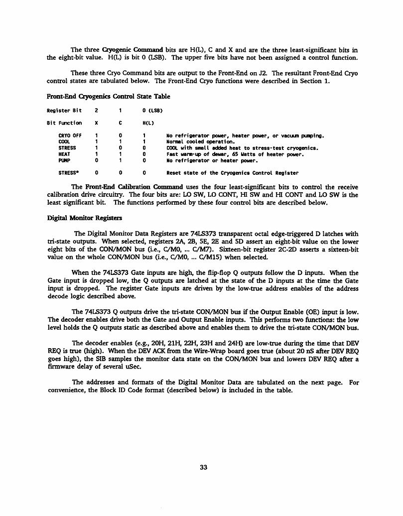
The three Cryogenic Command bits are H(L), C and X and are the three least-significant bits in the eight-bit value. H(L) is bit 0 (LSB). The upper five bits have not been assigned a control function.
These three Cryo Command bits are output to the Front-End on 32. The resultant Front-End Cryo control states are tabulated below. The Front-End Cryo functions were described in Section 1.
Front-End Cryogenics Control State Table
Register Bit 2 1 0 (LSB)
Bit Function X c H(L)
No refrigerator power, heater power, or vacuum pumping. Normal cooled operation. COOL with small added heat to stress-test cryogenics. Fast warm-up of dewar, 65 Watts of heater power. No refrigerator or heater power.
STRESS* 0 0 0 Reset state of the Cryogenics Control Register
The Front-End Calibration Command uses the four least-significant bits to control the receive calibration drive circuitry. The four bits are: LO SW, LO CONT, HI SW and HI CONT and LO SW is the least significant bit. The functions performed by these four control bits are described below.
Digital Monitor Registers
The Digital Monitor Data Registers are 74LS373 transparent octal edge-triggered D latches with tri-state outputs. When selected, registers 2A, 2B, 5E, 2E and 5D assert an eight-bit value on the lower eight bits of the CON/MON bus (i.e., C/MO, ... C/M7). Sixteen-bit register 2C-2D asserts a sixteen-bit value on the whole CON/MON bus (i.e., C/MO, ... C/M15) when selected.
When the 74LS373 Gate inputs are high, the flip-flop Q outputs follow the D inputs. When the Gate input is dropped low, the Q outputs are latched at the state of the D inputs at the time the Gate input is dropped. The register Gate inputs are driven by the low-true address enables of the address decode logic described above.
The 74LS373 Q outputs drive the tri-state CON/MON bus if the Output Enable (OE) input is low. The decoder enables drive both the Gate and Output Enable inputs. This performs two functions: the low level holds the Q outputs static as described above and enables diem to drive die tri-state CON/MON bus.
The decoder enables (e.g., 20H, 21H, 22H, 23H and 24H) are low-true during the time that DEV REQ is true (high). When the DEV ACK from the Wire-Wrap board goes true (about 20 nS after DEV REQ goes high), die SIB samples the monitor data state on the CON/MON bus and lowers DEV REQ after a firmware delay of several uSec.
The addresses and formats of the Digital Monitor Data are tabulated on the next page. For convenience, the Block ID Code format (described below) is included in the table.
33
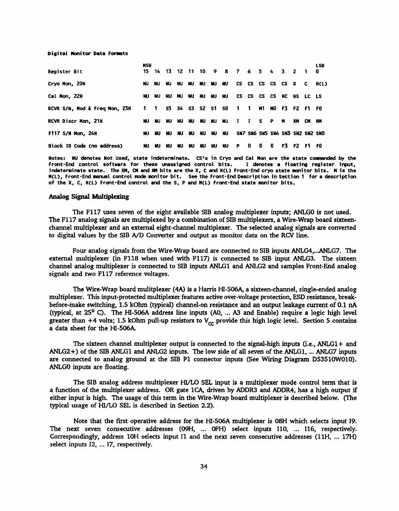
Digital Monitor Data Formats
HSB LSB Register Bit 15 14 13 12 11 10 9 8 7 6 5 4 3 2 1 0
Cryo Hon, 20H NU NU NU NU NU NU NU NU CS CS CS CS CS X C H(L)
Cal Hon, 22H NU NU NU MU NU NU NU NU CS CS CS CS HC HS LC LS
RCVR S/N, Mod & Freq Hon, 23H 1 1 S5 S4 S3 S2 SI SO 1 1 Ml MO F3 F2 Fl FO
RCVR Discr Hon, 21H NU NU NU NU NU NU NU NU I I S P M XM CM HM
F117 S/N Hon, 24H NU NU NU NU NU NU NU NU SN7 SN6 SN5 SN4 SN3 SN2 SN2 SNO
Block ID Code (no address) NU NU NU NU NU NU NU NU P 0 0 0 F3 F2 Fl FO
Notes: NU denotes Not Used, state indeterminate. CS's in Cryo and Cal Mon are the state commanded by the Front-End control software for these unassigned control bits. I denotes a floating register input, indeterminate state. The XM, CM and HM bits are the X, C and H(L) Front-End cryo state monitor bits. M is the M(L), Front-End manual control mode monitor bit. See the Front-End Description in Section 1 for a description of the X, C, H(L) Front-End control and the S, P and M(L) Front-End state monitor bits.
Analog Signal Multiplexing
The F117 uses seven of the eight available SIB analog multiplexer inputs; ANLGO is not used. The F117 analog signals are multiplexed by a combination of SIB multiplexers, a Wire-Wrap board sixteen- channel multiplexer and an external eight-channel multiplexer. The selected analog signals are converted to digital values by the SIB A/D Converter and output as monitor data on die RCV line.
Four analog signals from the Wire-Wrap board are connected to SIB inputs ANLG4,...ANLG7. The external multiplexer (in F118 when used with ¥117) is connected to SIB input ANLG3. The sixteen channel analog multiplexer is connected to SIB inputs ANLG1 and ANLG2 and samples Front-End analog signals and two F117 reference voltages.
The Wire-Wrap board mulitplexer (4A) is a Harris HI-506A, a sixteen-channel, single-ended analog multiplexer. This input-protected multiplexer features active over-voltage protection, ESD resistance, break- before-make switching, 1.5 kOhm (typical) channel-on resistance and an output leakage current of 0.1 nA (typical, at 25° C). The HI-506A address line inputs (AO, ... A3 and Enable) require a logic high level greater than +4 volts; 1.5 kOhm pull-up resistors to Vcc provide this high logic level. Section 5 contains a data sheet for the HI-506A.
The sixteen channel multiplexer output is connected to the signal-high inputs (i.e., ANLG1+ and ANLG2+) of the SIB ANLG1 and ANLG2 inputs. The low side of all seven of the ANLG1,... ANLG7 inputs are connected to analog ground at the SIB PI connector inputs (See Wiring Diagram D53510W010). ANLGO inputs are floating.
The SIB analog address multiplexer HI/LO SEL input is a multiplexer mode control term that is a function of the multiplexer address. OR gate 1CA, driven by ADDR3 and ADDR4, has a high output if either input is high. The usage of this term in the Wire-Wrap board multiplexer is described below. (The typical usage of HI/LO SEL is described in Section 2.2).
Note that the first operative address for the HI-506A multiplexer is 08H which selects input 19. The next seven consecutive addresses (09H, ... OFH) select inputs 110, ... 116, respectively. Correspondingly, address 10H selects input II and the next seven consecutive addresses (11H, ... 17H) select inputs 12, ... 17, respectively.
34

The ANENB feedback to the SIB is dependant upon the state of ADDR5. For the analog data multiplexing address range, (00H, ... 1FH, ADDR5 low), ANENB is true when qualified by DEV REQ. The ANENB response from the Wire-Wrap board is used to initiate the SIB analog multiplexing and A/D Converter operations. Note that when ADDR5 is false, the DEV ACK feedback to the SIB is inhibited.
The Analog Monitor Data address space, HI/LO SEL, ANLG inputs and multiplexed signals are tabulated on the next page. Note that when either ADDR3 or ADDR4 is a 1, HI/LO SEL (from gate 1CA) is a 1 which causes the SIB analog multiplexer to be driven by ADDR5, ADDR4 and ADDR3. In this condition, the multiplexers connected to ANLG1, ANLG2 and ANLG3 are driven by ADDR2, ADDR1 and ADDRO. This HI/LO SEL scheme constrains the analog address space to 20H addresses for a multiplexer channel capacity of 1FH (31 Decimal). Three spare channels are available in the F117: ANLGO, HI-506A inputs 115 and 116 - addresses 00H, OEH and OFH, respectively.
Analog Multiplexer Addresses and Signals
Addr, ADDR5 ADDR4 ADDR3 ADDR2 ADDR1 ADDRO ANLG HI/LO Selected Hex Input SEL Signal
00 0 0 0 0 0 0 0 0 NU - - - - - - - 1 - HI-H06A Mux, - - - - - - - 2 - see below 03 0 0 0 0 1 3 0 Ext Mux 04 0 0 0 1 0 4 0 Low Cal Current 05 0 0 0 1 0 5 0 HI Cal Current 06 0 0 0 1 6 0 Low Cal Voltage/4 07 0 0 0 1 7 0 HI Cal Voltage/4 08 0 0 0 VP 09 0 0 0 ACI 0A 0 0 0 LED 0B 0 0 0 SENS OC 0 0 1 +7.5 Ref 00 0 0 1 An Gnd 0E 0 0 1 NU OF 0 0 1 NU 10 0 0 0 2 LF1 11 0 0 0 2 RFI 12 0 0 0 2 LF2 13 0 0 0 2 RF2 14 0 0 1 2 15K 15 0 0 1 2 50K 16 0 0 1 2 300K 17 0 0 1 2 VD 18 0 0 0 0 3 External Mux Signal 19 0 0 0 3 H UN
1A 0 0 0 3 H II H
IB 0 0 3 11 II II
1C 0 1 0 0 3 II 11 II
ID 0 1 0 3 II II II
IE 0 1 0 3 M II II
Notes: NU denotes an unused analog input. The dashes indicate a "doesn't apply" case.
Calibration Switching Logic
The four Calibration control bits from the Calibration Command register are: LO SW, LO CONT, HI SW and HI CONT. LO SW is the least significant bit. Two sets of AND-OR gates drive the Cal and High Cal Drive circuitry (described below). These two sets of logic are independent of each other. The
35
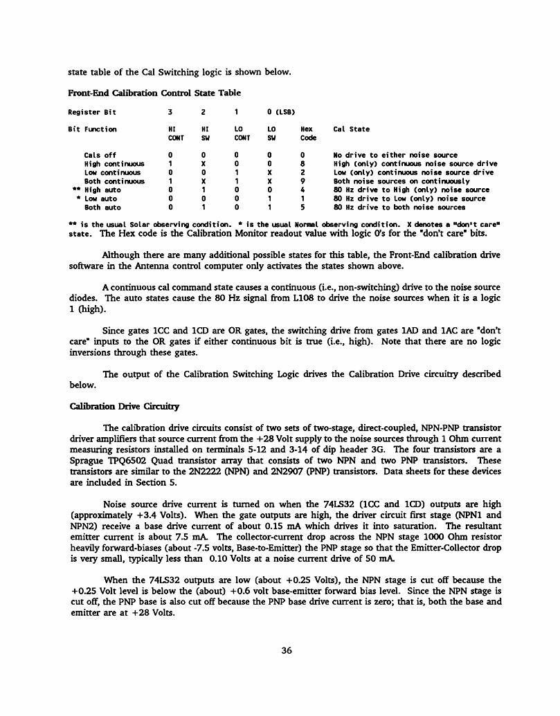
state table of the Cal Switching logic is shown below.
Front-End Calibration Control State Table
Register Bit 3 2 10 (LSB)
Bit Function HI HI LO LO Hex Cal State CONT SU CONT SU Code
Cals off 0 0 0 0 0 No drive to either noise source High continuous 1X008 High (only) continuous noise source drive Low continuous 0 0 1X2 Low (only) continuous noise source drive Both continuous 1X1X9 Both noise sources on continuously
** High auto 0 1 0 0 4 80 Hz drive to High (only) noise source * Low auto 0 0 0 1 1 80 Hz drive to Low (only) noise source
Both auto 0 1 0 1 5 80 Hz drive to both noise sources
** is the usual Solar observing condition. * is the usual Normal observing condition. X denotes a "don't care" state. The Hex code is the Calibration Monitor readout value with logic O's for the "don't care" bits.
Although there are many additional possible states for this table, the Front-End calibration drive software in the Antenna control computer only activates the states shown above.
A continuous cal command state causes a continuous (i.e., non-switching) drive to the noise source diodes. The auto states cause die 80 Hz signal from L108 to drive the noise sources when it is a logic 1 (high).
Since gates ICC and 1CD are OR gates, the switching drive from gates IAD and 1AC are "don't care" inputs to the OR gates if either continuous bit is true (i.e., high). Note that there are no logic inversions through these gates.
The output of the Calibration Switching Logic drives the Calibration Drive circuitry described below.
Calibration Drive Circuitry
The calibration drive circuits consist of two sets of two-stage, direct-coupled, NPN-PNP transistor driver amplifiers that source current from die +28 Volt supply to the noise sources through 1 Ohm current measuring resistors installed on terminals 5-12 and 3-14 of dip header 3G. The four transistors are a Sprague TPQ6502 Quad transistor array that consists of two NPN and two PNP transistors. These transistors are similar to the 2N2222 (NPN) and 2N2907 (PNP) transistors. Data sheets for these devices are included in Section 5.
Noise source drive current is turned on when die 74LS32 (ICC and 1CD) outputs are high (approximately +3.4 Volts). When the gate outputs are high, the driver circuit first stage (NPN1 and NPN2) receive a base drive current of about 0.15 mA which drives it into saturation. The resultant emitter current is about 7.5 mA. The collector-current drop across the NPN stage 1000 Ohm resistor heavily forward-biases (about -7.5 volts, Base-to-Emitter) the PNP stage so that the Emitter-Collector drop is very small, typically less than 0.10 Volts at a noise current drive of 50 mA.
When the 74LS32 outputs are low (about +0.25 Volts), the NPN stage is cut off because the +0.25 Volt level is below the (about) +0.6 volt base-emitter forward bias level. Since the NPN stage is cut off, the PNP base is also cut off because the PNP base drive current is zero; that is, both the base and emitter are at +28 Volts.
36
Calibration Current and Drive Voltage Monitor Circuitry
Referring to the amplifier circuit on the Wire-Wrap board schematic, note that noise source drive current is measured by two LF442A differential operational amplifiers. The amplifier difference signal inputs are the voltage drop across 1 Ohm (Rp) series resistors when the noise source is being driven. There are two divide-by-three voltage dividers to ground on each side of R- and the amplifier's + and - (positive and negative) inputs are connected to the junctions of the 10 K and 4870 Ohm resistors. When the 28 Volt noise source drive is on, these two points are about +9.2 Volts above ground; thus die LF442A amplifier's inputs have a common mode voltage of +9.2 Volts. This is not a problem because the LF442 can operate with common-mode inputs as high as +18 and -17 Volts and has a typical Common Mode Rejection Ratio of 100 dB (with a source impedance < 10 Ohms). The current flow into each divider circuit is about 28 Volts/15 kOhms or about 1.8 mA. The LF442A input impedance is greater than 1012
Ohms and input bias and offset currents are a few picoAmps at room temperature; therefore, the amplifier's output voltage is a simple function of the current difference in the two divider circuits. The two current monitor outputs are conected to the SIB ANLG 4+ and ANLG 5+ inputs (addresses 04H and 05H).
When there is a current flow through resistor Rp, the input to the divider connected to the amplifier - input is reduced by I^RQ Volts. The amplifier output swings positively to produce a current through the 100 kOhm feedback resistor to null the amplifier's error input. Since the feedback resistor is 100 kOhm (the divider current comes through a 10 kOhm resistor), the output voltage must swing ten times the voltage drop across R^ to drive an equivalent current into the amplifier's - input node. Another way of stating this is to note that the amplifier has a gain of 10: R-pe/R-mpuj = 10-
Since Rp is 1 Ohm, the current-voltage scaling of this amplifier is 100 mA/Volt. To obtain the value of noise source current, multiply the amplifier output voltage by 100 mA/Volt.
The - (negative) input divider has a 200 Ohm zero-adjustment pot to set the amplifier output to zero volts with the noise source voltage drive on but no load current
Section 5 has a data sheet for the LF442A amplifier.
The noise source drive voltage is monitored by a 40 kOhm, 4:1 voltage divider connected to the output side of Rp. The divider output is thus +7.00 Volts when the drive is active. (Note that the 0.7 mA current into mis divider goes through die 1 Ohm resistor; thus the amplifier's input difference includes the effect of this current. The divider outputs are connected to die SIB ANLG 6+ and ANLG 7+ inputs (addresses 06H and 07H).
In checking these monitor values when die antenna is observing, it is important to remember that the calibration circuitry is normally in the auto mode; values read in this mode will vary because the data sampling time and switching signal are not concurrent. Correct values may be read by setting the calibration command to the continuous-on states shown in the table above.
Calibration Drive Inhibit Circuitry
A drive inhibit circuit protects the noise sources from excess current drive. Two LM393A analog comparators force the drive to the NPN-PNP driver circuit (described above) to ground if the output of the current monitor circuit (described above) exceeds +1.9 volts. This level is determined by the tap on die R53-R54 voltage divider connected to the + (plus) inputs of the LM393A,s.
When an analog comparator's + (plus, noninverting) input is more positive than the - (minus) input, the output is positive (high) and when the + input is more negative than the - input, the output
37

is negative (low). Typically, only a few millivolts are required to cause the switching transitions because an analog comparator is essentially a high-gain operational amplifier without feedback.
In the inhibit circuit, the - input is connected to the current monitor amplifier's output and the + input is connected to the +1.9 Volt tap on the voltage divider. When the voltage from the current monitor is less than +1.9 Volts, the comparator output is high; this enables the driver circuit to output current to the noise sources. If the voltage from the noise source monitor circuit exceeds the +1.9 Volt level, the comparator output drops to ground. This inhibits the driver circuits because the 74LS32 base drive current for the NPN1 and NPN2 transitors is diverted to ground.
The LM393A comparator has an open-collector output; when high, it assumes the level of the NPN-PNP transistor driver circuit input. When low, the level is about 10 mVolts when sinking the 0.15 mA drive from the 74LS32 gate. This low level imposes a hard limit on the input to the NPN-PNP transistor driver circuit.
Section 5 contains a data sheet for die LM393A.
A 75141 dual, single-ended line Front-End is used to detect the 80 Hz Mod signal from L108. This Front-End can function as a level comparator by connecting the Common Reference input to a reference voltage, in this case the +1.9 Volts used by the inhibit circuitry described above. +1.9 volts is slighdy less than the typical 74LS 2 Volt VIH. The 75141 output is inverted relative to the input; if the MOD signal is high (and 100 mV above +1.9 Volts), the output is low and the cal switching logic outputs are low (if set to the switching mode). If the Mod signal is about 100 mV less than +1.9 V, the output is high and the switching logic output is also high. The 75141 outputs are TTL-compatible.
Section 5 contains a data sheet for the 75141.
Device ID Code Register
Register 5E, a 74LS373 octal latch, performs the function of asserting the Block ID code on the lower eight bits of the CON/MON bus when the ID REQ line from the SIB drops low. The Block ID code bits are the Front-End Band Code (bits F3, .. FO) and the even parity bit PA(L) (shown as P in the table above) and are stored in the register Q outputs when the ID REQ line is high. Three of the eight bits are set to logic O's and Inverter IBB makes the parity odd as required by die MCB specifications. The usage of the Block ID code was described in the MCB description above.
Power Reset Circuitry
A power reset circuit clears die command registers when +5 Volt power is applied to the module. The circuit is identical to that used on the SIB and uses a 74LS221 Schmidt input one-shot. When power is applied, the 22 uF capacitor charges to +5 Volts through die 1 kOhm resistor; the one-shot triggers when the capacitor voltage reaches the B input 1 Volt (typical) threshold. The time delay to the trigger threshold is about 32 ms (assuming that the 5-Volt power is a step). The 74LS221 triggers reliably on input signals having slopes as low as 1 Volt/second. A dV/dt, this low permits the RC delay circuit to have a large time constant so that a long delay is realized after power is applied. The one-shot delay time is about 100 ms which clears the two 74LS273 command registers. The diode across the charging resistor protects the one-shot input from being forced to -5 Volts by the charged capacitor when the power is removed.
38

Module Serial Number Register Encoding
The F117 module serial number is read from register 5D, a 74LS373 transparent octal latch. The register loading process was described above. When the module is manufactured, a high-true binary module serial number code is wired onto the Wire-Wrap connector pins. 1's code bits are set by connecting the associated pins to +5 Volts on pin W28. O's code bits are set by connecting the associated pins to logic common on pin W27.
75 Volt Reference
Two reference voltages connected to inputs on the 16-channel analog multiplexer provide a means of checking die SIB analog multiplexer and A/D Converter gain and zero drift. These two voltages are analog common and +7.5 Volts. The +7.5 Volt reference is provided by an Analog Devices AD584JH pin- programmable voltage reference installed on a transistor adaptor at location 3C. AD584 pins 1 and 2 are jumpered to program a +7.5 Volt output. The maximum error of this output over the 0 to 70° C temperature range is +/- 30 mV. Section 5 contains a data sheet for the AD584.
39

40
3.0 BENCH TEST AND AUGNMENT
This section describes the F117 Bench Test and Alignment system used at the AOC Front-End Laboratory; this is the primary maintenance and alignment facility for the F117 module. The system consists of the Test Environment, the Test Fixture and the the Test Program.
F117 Test Environment
The Test Environment simulates the F117 operating environment and consists of an IBM- compatible PC to execute the test program, an RS-232/RS-485 line signal converter to adapt the PCs RS- 232 serial I/O levels to the SIB's RS-485 levels, the F117 Loop-Back Unit for both digital and analog simulation and +5, +/-15 and +28 Volt power supplies. The F117 Test Environment is depicted on Figure 7 (this page).
F117 Test Fixture
The F117 Loop Back Unit schematic diagram is drawing C53510S005 and the assembly drawing is C53510A007. This test fixture has two cables that terminate in 25-contact "D" connectors that are plugged into F117 front panel connectors Jl (Front-End monitor) and 32 (Front-End control). A single wire from the Loop Back unit (RTP7, X Cmd) connects to the F117 module rear panel (Jll- 12, MOD signal input). Under test program control, this X command simulates the MOD calibration switching command to the F117. The Loop Back unifs circuitry is powered by + and -15 volts from J2, the Front- End control connector.
The F117 Loop Back unifs stimulus inputs are the PUT'S three multiplexer address lines (ADDRO, ADDR1, ADDR2) and the three Front-End cryogenic control bits X, C and H(L). (H is used to designate H(L) in the following discussion.) These six signals exercise the F117 Loop Back unit circuitry.
The Loop Back provides Front-End Band Code and Parity Bit (even), hard-wired to logic common; this designates a Block IDN code (N in SIB terminology) of 0 which designates an FE101 (75 MHz) Front- End. (See the table of Band Codes in Section 1.0 and the Block IDN code format in Section 2.3. Schematic Diagram D53510S004 depicts the F117s Band Code and Block IDN logic circuitry.)
The state of X (one of the three cryogenic control bits) controls the selection of the analog signal level input to the Front-End analog inputs on Jl. When X is a "1" (high), zero volts are input to all analog inputs via unity-gain buffers; when X is a "0", +8.3 volts are input to the analog inputs. The external analog multiplexr, ANLG3 (also on Jl) is also driven by the X-controlled zero and +8.3 volts. As noted above, X is also fed back to the F117 module MOD input to simulate the MOD signal for the Cal Switching tests.
The X, C and H cryogenic control bits are also connected to the X Mon, C Mon and H Mon
MOD
80X86 PC 838/483
CONV a +/-15V.
+5V, +28V PUR SUPP
F117 Jll
Jl
J2
I I
LOOP
BACK
UNIT
Figure 7, F117 Test Environment
41
inputs to simulate these three Front-End state discretes.
The inverse of the states of the C and H bits are connected to the Front-End Serial Number and Modification Level inputs on J2. The truth table for these inputs as a function of the C and H bits is shown below.
Cmd Bits Front-Er td Serial Nunbei - Code Bits Rcvr Code, Hex
Mod Lvl Bits Hod Lvl, Hex
C H S5 S4 S3 S2 SI so HI HO
0 0 1 1 1 1 1 1 3F 1 1 3 0 1 1 0 1 0 1 0 2A 1 0 2 1 0 0 1 0 1 0 1 15 0 1 1
F117 Multiplex Address bits ADDRO, ADDR1 and ADDR2 are connected to the Jl Front-End control and status monitor discretes M Mon (Front-End Control in Manual Control Mode), P (Pump Request) and S (Vacuum Solenoid Monitor), respectively.
Resistors 1 and 2 (Rl and R2, both 1000 Ohms, 2 Watt) are loads for the High Calibration and Calibration drive circuitry in J117.
F117 Test Program
The following text is a narrative description of the operations performed by the F117 test progam in exercising an F117 connected to the F117 Loop Back Unit or die F117 connected to a Front-End for Front-End monitoring (described below). Since the text emphasis is on a description of the test functions, it is too long and detailed to be a convenient test procedure although it does include some operator- program interactions. During the course of program execution, several CRT dislays show the states of the F117 tests or Front-End being monitored. The text includes samples that were printed by the test systen.
Secondly, it is not a description of the program or its mechanics but there are some program references. For example, the notation Page 5B refers to an operation performed on the bottom of Page 5 in die source code listing (in Section 6). Some variables such as MONCHAR$(XX, Z), constants like &HF0 or a flag like FLAGER3 are mentioned where it seems appropriate to do so. Although this text is not a program description, it may be a useful reference for modifications to the program or an adaptation of some elements of the program to another test application involving the SIB.
The F117 test program is F117.EXE and the source code is F117_2.BAS (described below). The program's initial operation is a test of the SIB; if problems are detected, the SIB board should be replaced. If the SIB passes these initial tests, the program proceeds to perform a comprehensive functional test of the F117 module.
The F117_2.BAS Test Program is written in Microsoft Basic and then compiled to F117.EXE. The program description is based upon the February 1, 1993 version but there may be future changes to implement more extensive analyses of the PUT'S or Front-End's performance.
The program may be run from the DOS root directory by typing F117 followed by ENTER.
The test program has three operating modes: 1) The Auto-Loop mode in which test program functions proceed automatically and provide a go/no-go test result at the completion of the test. 2) The Man-Loop mode performs the same test operations as 1) above, but there are pauses at important points in the program to permit direct manual measurements of F117 states; the test sequence may be resumed after the pauses. In the Auto-Loop mode, failure of certain tests forces a transition to the Man-Loop
42
mode to enable the operator to make manual F117 adjustments or measurements. It is not possible to make a transition from the Man-Loop mode to the Auto-Loop mode. 3) The Front-End Monitor mode in which a Front-End (instead of the F117 Test Fixture) is connected to the PUT'S Jl and J2 connectors with 25-conductor cables. The Front-End (not the ¥117) is the focus of this test mode and a fully- functional F117 is required to avoid ambiguities in the tests. The Front-End's RF inputs are the ambient RF levels of the lab environment; the RF output signals are not tested but the calibration noise sources are powered. The Front-End's Calibration drive and Cryogenic control inputs are exercised and its analog and digital outputs are monitored via the F117 circuitry. This mode provides a convenient way to systematically exercise the Front-End's cryogenics and calibration circuitry, monitor the Front-End's analog and digital signals and trouble-shoot Front-End signal and wiring problems. The Front-End Monitor mode performs the same test operations as 1) above, but permits die operator to enter cryogenic and calibration command states. Once entered, there are no transitions from die Front-End Monitor mode to the other test modes.
The F117 test program is a single entity, not three separate sub-programs; program flow is a function of the operating modes. A third-party serial I/O subroutine is called to control the serial port operations.
In the text below, all operator interactions and test result messages are indicated by BOLD CAPS TEXT. The operator interacts with the program execution by inputting manual commands at certain points during the execution when prompted by messages on the CRT. These manual command inputs are all cited in BOLD CAPS TEXT. Test result messages and data are also displayed on the CRT as BOLD CAPS TEXT. These messages are sometimes single lines, other times a part of a CRT display. Samples of these displays are pictured in the text below.
Before starting the program execution, the OPERATOR SHOULD TURN OFF THE F117 + 5 AND +/- 15 VOLT POWER SUPPLIES FOR AT LEAST 5 SECONDS. This permits the SIB power reset circuit capacitors to discharge; when power is reapplied, the power reset circuit initiates a processor reset which activates initialization firmware. The initialization firmware reads the Block IDN value and sets the address block start address and block size parameters to default values. The first operations of the test program evaluate the reset conditions. If die CRT displays the message "MONCHAR$(mimber) SUBSCRIPT OUT OF RANGE", it indicates that either the SIB power had not been turned off, or the off period was too short or that the SIB initialization is not working.
When the program is started, the CRT displays a box showing: "VLBA F117 MODULE TEST PROGRAM & FE MONITOR by LDM MAR 92" followed by "needs: F117, F117 test box / pwr supply, F117 cables & RS232 cable".
The CRT then displays a sequence of four messages that prompt the operator to make the following cable connections; the operator should respond to each of these messages by pressing ENTER. These messages are: "Connect F117 rear cables to Willy box, press ENTER when ready". "Connect RS232 cables to Willy box & PC, press ENTER when ready". "Connect F117 front jumpers, press ENTER when ready". "Connect ac power to F117 & turn ON, press ENTER when ready".
A program control flag, FLAGER3 (evoked from the operator), determines the program's operating mode (described below). This flag is tested at strategic locations in the program and determines the program flow as a function of the operating mode. If the operator FLAGER3 = 1, the Man-Loop mode is specified; if FLAGER3 = 2, the Auto-Loop mode is specified; and finally, if FLAGER3 = 3, the FE Monitor mode is specified. FLAGER3 is input on page 2T (T for Top of page). The CRT displays a mode selection menu in a box which has a "SEI£CT designator, "1, 2, 3 or Q" to be input by the operator to designate the "F117 MAN LOOP TEST, F117 AUTO LOOP TEST OR FRONT END MONITOR" modes, respectively. The SELECT value (1, 2 or 3) is FLAGER3 in the program. "Q" designates Quit for stop
43
program execution.
The operator is next prompted to verify that the cable configuration is correct for the selected mode (Page 2T). In the Man-Loop or Auto-Loop modes, the CRT displays "BE SURE TO CONNECT FRONT LOOP BACK TEST JUMPER ON F117" followed by "PRESS ENTER TO CONTINUE". In the FE Monitor mode, the CRT displays "BE SURE TO CONNECT FE CABLES TO F117" followed by "PRESS ENTER TO CONTINUE".
Since the SIB is the control-data interface to the F117, it is tested first in all three modes. A delay subroutine, DELAY! (page 36M) is frequently called to insert time delays in the program execution to provide sufficient time for the serial I/O operations to be completed.
The first operation of the program (common to all three modes) is a readout of the 16 (MDH and MDL) monitor data values stored in the SIB's last 16 data addresses (see the description of these values in Section 2.2) The CRT displays "PRECHEK MON WORDS". This operation begins on page 2M. These values are intialized by the 8032 Microcontroller firmware when the SIB is powered up (mentioned above). Important parameters are N (labelled IDN in the program), the Block IDN Code read from the Device (i.e. ¥117), the SIB Type and Revision (Version "D", Rev "B") and the Block Start Address. The Block Start Address is initialized to 7FF0H and remains set at this value until set to another value by the MCB Controller (i.e. the Station Computer, in this case the F117 Test System). The Block Size is initialized to 16 to permit these 16 monitor data values to be read out.
For convenience in the following discussion, these initial end-of-block parameters are as follows:
BE-X EOB Function Addr AddrH
BE-15 7FF0 Reserved for future use, 7FF0H is the Block Start Address BE-14 7FF1 " " " " BE-13 7FF2 " H " " BE-12 7FF3 No Control Response Counter (i.e., no DEV ACK from Device) BE-11 7FF4 No Monitor Response Counter (i.e., no DEV ACK or ANENB from Device) BE-10* 7FF5 Interface Type and Revision Code. For F117 should be D and B (Version D, Rev B) BE-9 7FF6 Address of most recent control message (i.e., ADH and ADL) BE-8 7FF7 Control Data for most recent control message (i.e., CDH and CDL) BE-7 7FF8 Address parity error counter, all messages BE-6 7FF9 Control data parity error counter, all messages BE-5 7FFA Invalid SYN character counter, all messages BE-4 7FFB Control Data parity error counter, messages in block BE-3* 7FFC IDN (Block ID code value from F117, 0, for F117 Test Fixture) BE-2 7FFD Count of correctly received control messages BE-1 7FFE Count of correctly received monitor data request messages BE-0 7FFF Address of beginning of block (0100H for the F117 test fixture)
* Cannot be altered by the Controller or F117 test program
The monitor data read process stores these data values in the MONCHARS array (16 elements, 3 bytes/element, i.e. for ACK, MDH and MDL) during the first phases of program execution. Since these memory locations in the SIB RAM are initialized to specific states during the processor power-up initialization, the test program reads and tests the values to verify that the SIB is responding properly to monitor data request messages and to evaluate the quality of the SIB-MCB interactions.
The other values in the table (three are unassigned) are address and data values (of the most recent control and data messages) and several error counters. These parameters are not important at this stage of the test program but are printed out (page 3T) for the operator's information (the error counters should all be zero). Note that die count values in locations BE-2 and BE-1 are not errors and will increase
44
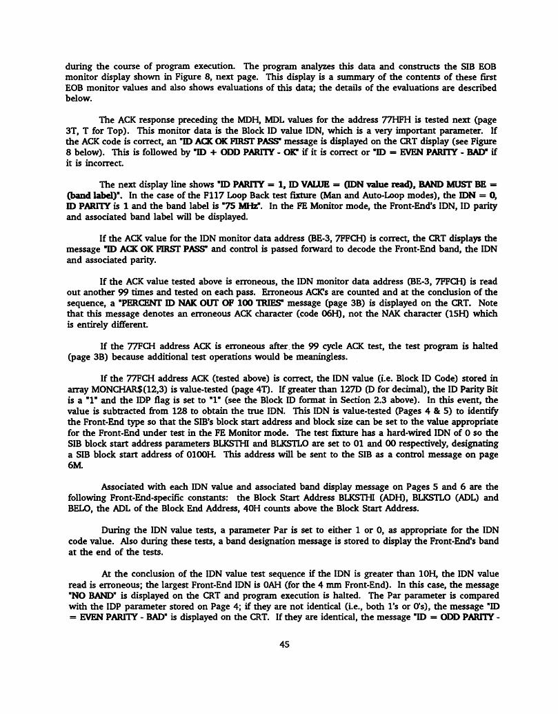
during the course of program execution. The program analyzes this data and constructs the SIB EOB monitor display shown in Figure 8, next page. This display is a summary of the contents of these first EOB monitor values and also shows evaluations of this data; the details of the evaluations are described below.
The ACK response preceding the MDH, MDL values for the address 77HFH is tested next (page 3T, T for Top). This monitor data is the Block ID value IDN, which is a very important parameter. If the ACK code is correct, an "ID ACK OK FIRST PASS" message is displayed on the CRT display (see Figure 8 below). This is followed by "ID + ODD PARITY - OKT if it is correct or "ID = EVEN PARITY - BAD" if it is incorrect.
The next display line shows "ID PARITY = 1, ID VALUE = (IDN value read), BAND MUST BE = (band label)". In the case of the F117 Loop Back test fixture (Man and Auto-Loop modes), the IDN = 0, ID PARITY is 1 and the band label is "75 MHz". In the FE Monitor mode, the Front-End's IDN, ID parity and associated band label will be displayed.
If the ACK value for the IDN monitor data address (BE-3, 7FFCH) is correct, the CRT displays the message "ID ACK OK FIRST PASS" and control is passed forward to decode the Front-End band, the IDN and associated parity.
If the ACK value tested above is erroneous, the IDN monitor data address (BE-3, 7FFCH) is read out another 99 times and tested on each pass. Erroneous AOCs are counted and at the conclusion of the sequence, a "PERCENT ID NAK OUT OF 100 TRIES" message (page 3B) is displayed on the CRT. Note that this message denotes an erroneous ACK character (code 06H), not the NAK character (15H) which is entirely different.
If the 77FCH address ACK is erroneous after the 99 cycle ACK test, the test program is halted (page 3B) because additional test operations would be meaningless.
If the 77FCH address ACK (tested above) is correct, the IDN value (i.e. Block ID Code) stored in array MONCHAR$(12,3) is value-tested (page 4T). If greater than 127D (D for decimal), the ID Parity Bit is a "1" and the IDP flag is set to "1" (see the Block ID format in Section 2.3 above). In this event, the value is subtracted from 128 to obtain the true IDN. This IDN is value-tested (Pages 4 & 5) to identify the Front-End type so that die SIB's block start address and block size can be set to the value appropriate for the Front-End under test in the FE Monitor mode. The test fixture has a hard-wired IDN of 0 so die SIB block start address parameters BLKSTHI and BLKSTLO are set to 01 and 00 respectively, designating a SIB block start address of 0100H. This address will be sent to the SIB as a control message on page 6M.
Associated with each IDN value and associated band display message on Pages 5 and 6 are the following Front-End-specific constants: the Block Start Address BLKSTHI (ADH), BLKSTLO (ADL) and BELO, the ADL of the Block End Address, 40H counts above the Block Start Address.
During the IDN value tests, a parameter Par is set to either 1 or 0, as appropriate for the IDN code value. Also during these tests, a band designation message is stored to display the Front-End's band at the end of the tests.
At the conclusion of the IDN value test sequence if the IDN is greater than 10H, the IDN value read is erroneous; the largest Front-End IDN is OAH (for the 4 mm Front-End). In this case, the message "NO BAND" is displayed on the CRT and program execution is halted. The Par parameter is compared with the IDP parameter stored on Page 4; if they are not identical (i.e., both 1's or O's), the message "ID = EVEN PARITY - BAD" is displayed on the CRT. If they are identical, the message "ID = ODD PARITY -
45
OK" is displayed. The band designation message (e.g., "75 MHz" for the test fixture IDN) is also displayed.
If the program did not halt as a result of a failure of the test immediately above, the ACK character for all 16 monitor data readout values in the MONCHARS array are tested (page 7B). If any of the 16 ACK codes is incorrect, the message "NO ACK ONE OR MORE INITIAL MON WORDS" is displayed. If they are all correct, the message "ALL ACK OK IN FIRST PASS" is displayed.
Following the test of the 16 ACK values above, the error counter values (bytes 2 and 3) in the first 14 sets of the MONCHARS array are tested for a zero value (Page 5); the SIB should have initialized these counters to zero. The BE-10 (address 7FF5H, SIB Version and Rev values, D and B respectively) and BE-3 (8032 address 7FFC, IDN) are excluded from the zero-value test because they are never zero. If all of the 12 sets of MDH and MDL values tested are zero, the message "ALL MON WORDS THAT SHOULD BE ZERO - ARE ZERO". If any of the 12 sets of MDH and MDL values tested are not zero, the message "ONE OR MORE MON WORDS NOT ZERO THAT SHOULD BE" is displayed on the CRT. If these words are not all zero, program operation still continues to the 99-cycle loop below.
The final test in this part of the program is to read and display the SIB Version and Revision level (Page 6T). MONCHAR$(5,2) contents are the SIB Version (should be "D") and MONCHAR$(5,3) contents are the SIB Revision (should be "B"). These were read from BE-5 location and are displayed on the CRT with the messages "INTERFACE TYPE = D INTERFACE REVISION = B". The program does not test these values; THE OPERATOR SHOULD VERIFY THEM.
The tests above showed that if successful for at least 16 monitor data requests, the SIB response was correct for its initialized state. The next test (page 67) is a more extensive exercise of the SIB that reads and evaluates these 16 Block-End monitor values in a 99-cycle loop. The 99-cycle loop test repeats the 16-address, single-pass operation described above. The objective of this 99-cycle loop test is to request a lot of monitor data (1584 monitor data readouts) and to test the known values (ACK, IDN, SIB Version and Rev), and to assess the error counter accumulations. If the test environment power is glitch-free and the MCB is not faulty, the SIB error rates should be zero and all the fixed values such as ACK, IDN and SIB Version and Rev should never be incorrect.
Much of the 99-cycle loop code is a replica of the operations described above. During each pass the CRT displays "CHECKING ALL FIRST 16 SIB MON WORDS 100 TIMES - CHECK # (pass number)".
The first operation in the 99-cycle FOR-NEXT loop reads the 16 three-bytes sets of End-Block monitor data and loads it into the MONCHARS array in a 16-cycle FOR-NEXT loop. Unlike the comparable portion of the code above, the 16 sets of data are not printed. This code (Page 6) is virtually a replica of the Page 3 code.
After this data has been stored in the MONCHARS array, the next operation in the 99-cycle loop is to test the 16 ACK characters in the MONCHARS array (page 10T). Each set consists of three bytes; ACK is the first byte in each set. If any of the 16 ACK characters is erroneous, a "NO ACK ONE OR MORE SUBSEQUENT MON WORDS" message is displayed on the CRT. This code is virtually a replica of the Page 5 code.
The next operation in the 99-cycle loop is to test the 13 error counters to verify that they are all zero (Page 7). If one or more error counter values are not zero, the "ONE OR MORE MON WORDS NOT ZERO THAT SHOULD BE" message is displayed on the CRT. This code is virtually a replica of the comparable Page 5 code.
The 99-cycle loop will increment the BE-1 counter which contains a count of the number of
46
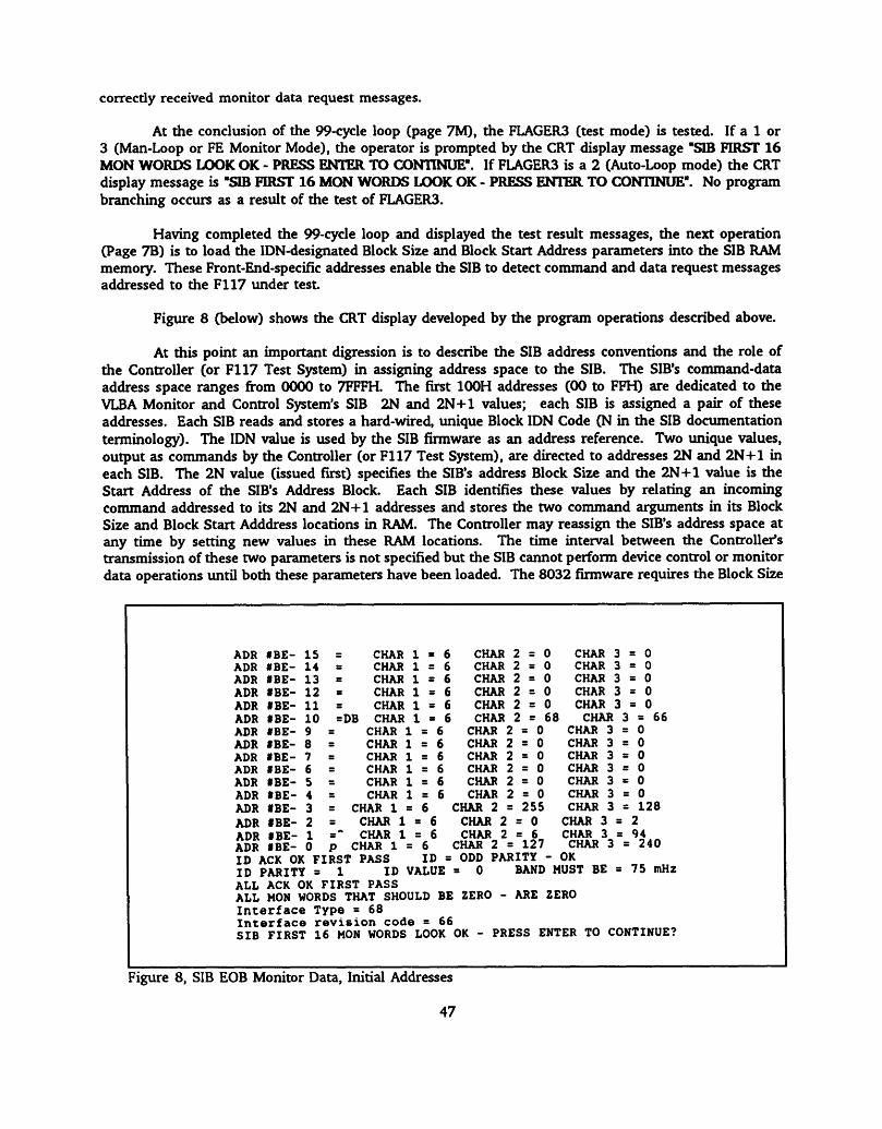
correcdy received monitor data request messages.
At the conclusion of the 99-cycle loop (page 7M), the FLAGER3 (test mode) is tested. If a 1 or 3 (Man-Loop or FE Monitor Mode), the operator is prompted by the CRT display message "SIB FIRST 16 MON WORDS LOOK OK - PRESS ENTER TO CONTINUE". If FLAGER3 is a 2 (Auto-Loop mode) the CRT display message is "SIB FIRST 16 MON WORDS LOOK OK - PRESS ENTER TO CONTINUE". No program branching occurs as a result of the test of FLAGER3.
Having completed the 99-cycle loop and displayed the test result messages, the next operation (Page 7B) is to load the IDN-designated Block Size and Block Start Address parameters into the SIB RAM memory. These Front-End-specific addresses enable the SIB to detect command and data request messages addressed to the F117 under test.
Figure 8 (below) shows the CRT display developed by the program operations described above.
At this point an important digression is to describe the SIB address conventions and the role of the Controller (or F117 Test System) in assigning address space to the SIB. The SIB's command-data address space ranges from 0000 to 7FFFH. The first 100H addresses (00 to FFH) are dedicated to the VLBA Monitor and Control System's SIB 2N and 2N+1 values; each SIB is assigned a pair of these addresses. Each SIB reads and stores a hard-wired, unique Block IDN Code (N in the SIB documentation terminology). The IDN value is used by the SIB firmware as an address reference. Two unique values, output as commands by the Controller (or F117 Test System), are directed to addresses 2N and 2N+1 in each SIB. The 2N value (issued first) specifies the SIB's address Block Size and the 2N+1 value is the Start Address of the SIB's Address Block. Each SIB identifies these values by relating an incoming command addressed to its 2N and 2N+1 addresses and stores the two command arguments in its Block Size and Block Start Adddress locations in RAM. The Controller may reassign the SIB's address space at any time by setting new values in these RAM locations. The time interval between the Controller's transmission of these two parameters is not specified but the SIB cannot perform device control or monitor data operations until both these parameters have been loaded. The 8032 firmware requires the Block Size
ADR «BE- 15 = CHAR 1 * 6 CHAR 2=0 CHAR 3=0 ADR «BE- 14 = CHAR 1*6 CHAR 2=0 CHAR 3=0 ADR #BE- 13 = CHAR 1*6 CHAR 2=0 CHAR 3=0 ADR #BE- 12 = CHAR 1=6 CHAR 2=0 CHAR 3=0 ADR »BE- 11 = CHAR 1=6 CHAR 2=0 CHAR 3=0 ADR #BE- 10 =DB CHAR 1=6 CHAR 2 = 68 CHAR 3 = 66 ADR #BE- 9 = CHAR 1=6 CHAR 2=0 CHAR 3=0 ADR #BE- 8 = CHAR 1=6 CHAR 2=0 CHAR 3=0 ADR #BE- 7 = CHAR 1=6 CHAR 2=0 CHAR 3=0 ADR #BE- 6 = CHAR 1=6 CHAR 2=0 CHAR 3=0 ADR #BE- 5 = CHAR 1=6 CHAR 2=0 CHAR 3=0 ADR #BE- 4 = CHAR 1=6 CHAR 2=0 CHAR 3=0 ADR #BE- 3 = CHAR 1=6 CHAR 2 = 255 CHAR 3 = 128 ADR #BE- 2 = CHAR 1=6 CHAR 2=0 CHAR 3=2 ADR «BE- 1 a* CHAR 1=6 CHAR 2=6 CHAR 3 = 94 ADR »BE- 0 p CHAR 1=6 CHAR 2 = 127 CHAR 3 = 240 ID ACK OK FIRST PASS ID = ODD PARITY - OK ID PARITY =1 ID VALUE = 0 BAND MUST BE = 75 mHz ALL ACK OK FIRST PASS ALL MON WORDS THAT SHOULD BE ZERO - ARE ZERO Interface Type = 68 Interface revision code = 66 SIB FIRST 16 MON WORDS LOOK OK - PRESS ENTER TO CONTINUE?
Figure 8, SIB EOB Monitor Data, Initial Addresses
47
value before the Block Start Address.
Consider some examples: the 75 MHz Front-End's IDN is 0, the 2N address is thus 00H and the 2N+1 address is 01H. The Controller sends 40H (the Block Size) to address 00 (2N address) and 0100H (the Block Start Address) to address 01 (2N+1 address). The 2.3 GHz Front-End's IDN is 3, the 2N address is 06H and the 2N+1 address is 07H. The Controller sends 40H to address 06H (2N) and sends 280H (the Block Start Address) to address 07H (2N+1). The IDN values for each band are tabulated in Section 1.
The ADH for these two commands is 80H; the most-significant bit is a "1" to designate a command message.
When the SIB is powered up, as described above, the 8032 firmware exercises the initialization code which stores a default block size (10H) and block start address (7FF0H) in the 2N and 2N+1 RAM locations. The usage of these last 16 addresses was described above.
The first operation in sending die Block Size and Block Start Address values is to set 1's in all locations of the MONCHARS array (Page 7B).
The page 7B code is general in that it will enable all possible Front-End Block Start address values to be loaded into the SIB as a function of the IDN. In the Man-Loop and Auto-Loop modes, the IDN for the F117 Test Fixture is a hard-wired code of 0 so the Block Start address is commanded to 0100H. If a front-end is connected to the F117 (for the FE Monitor mode tests), the Block Start address will be set to the appropriate value as a function of the IDN value. The Block Size for all Front-Ends is 40H.
Page 7B assigns values to the ADL portions of the 2N and 2N+1 addresses for each IDN. They are labelled CADR1LO and CADR2LO and are used in sending these values to the SIB on Pages 8 and 9. The IDN, CADRILO and CADR2LO values are displayed on the CRT with these labels (Page 8M).
After sending the Block Size (2N) command to the SIB, the Com Routine sends out a monitor data request to the 2N address to read back the 2N address data to confirm that it has been loaded. A message "BLOCK SIZE COMMAND RESPONSE = (block size)" is displayed on the CRT. This is followed by the CRT message "JUST SENT BLOCK SIZE COMMAND".
The Block Start Address must now be sent to die SIB (Page 9T). Following this transmission, the value is read from the SIB and the CRT displays the message "BLOCK START ADDRESS RESPONSE = (block start address)".
The error counter PERROR is cleared (Page 9B), the MONCHARS array is cleared to O's and the message "STARTING RECHECK OF RELOCATED MON WORDS" is displayed on the CRT (Page lOT). This operation will read back all 16 end-of-block monitor values in a 16-cycle For-Next loop.
The ADH (BLKSTHI, from Page 4) for this set is transmitted next (Page 10M). The ADL for the first address is 30H, 10H counts less than 40H, so the ADL (for IDN = 0) is H30; this is transmitted next Note that there are two possible values for ADL as a function of the Block Start Address intervals (80H). If the intervals were 100H, the end-block ADL addresses would be identical. CDH and CDL values of 00H are transmitted following ADL. The data values are loaded into the MONCHARS array.
The 16 end-of-block monitor values read back in the 16-cycle For-Next loop are printed out in the format shown in Figure 9, next page. Note that this data display is very similar to that shown in Figure 8, above. The operations described immediately below generate and display this data.
48

After storage and print-out of the 16 sets of values, the ACK character for the IDN address (ADL = HFC) is checked; this operation is identical to that on Page 3. If it is correct, the message "Relocated ID ACK OK FIRST PASS" is displayed on the CRT.
If the IDN message ACK is bad, this message element (for the 13th value) is read in a 99-cycle FOR-NEXT loop (Page 11M). This test is similar to that performed on Page 3B but does not read the whole 16-value set. Before this loop is started, the MONCHARS array is cleared to O's. At the completion of this 99-cycle loop, the message "relocated PERCENT ID NAK OUT OF 100 TRIES = (percent value)" is displayed on the CRT screen. This is a test of die ACK character 06H, not NAK which is 15H.
Following this ACK error analysis (if it was entered) or if the single IDN ACK test of two paragraphs above was passed, the IDN parity (of the single-pass or the last IDN message tested in the 99- pass try) is determined (Page 12B). The BANDS value is set to indicate the Front-End's frequency band (75 MHz for the F117 Test Fixture) and the two parameters CBLKSTHI and MBLKSTW (for the first addresses of the Wire-Wrap board control and monitor data addresses) are set for subsequent use in the program.
If the IDN is greater than 10, the BANDS parameter is set to "NO BAND" (an erroneous state) and if Par is not equal to IDP, the message "ID = EVEN PARITY - BAD" is displayed on the CRT (Page 12B). If the IDP parity is not erroneous, the messages "ID PARITY = (Value), ID VALUE = (Value) and BAND MUST BE = (Value) are displayed. (The Par parameter test was described in the Page 5B code above).
On Page 13T, all 16 ACK characters in the MONCHARS array are tested; these were loaded by the single pass end-of-block data read operation on Page 11T. If any ACICs are missing, the message "NO ACK ONE OR MORE relocated INITIAL MON WORDS" is displayed on the CRT. If all ACICs are correct, the message "ALL relocated ACK OK FIRST PASS" is displayed on the CRT.
On Page 13M, the error counters are tested for Cs; if any of these twelve counter contents are not zero, the message "ONE OR MORE relocated MON WORDS NOT ZERO THAT SHOULD BE" is displayed on the CRT. If these counter contents are all zero, the message "ALL relocated MON WORDS THAT SHOULD BE ZERO - ARE ZERO" is displayed on the CRT.
Following these analyses, on Page 13B the message "relocated Interface Type = (Type), relocated Interface revision code = (Rev)" is displayed on the CRT.
The analyses above are based upon a single pass through die 16 monitor data messages. On Page 13B, these 16 values are tested in a 100-cycle loop. This test is similar to that performed on Page 6T for the initialized set of addresses (i.e. 7FF0H to 7FFF). The purpose of this test is to evaluate the SIB's performance when it is subjected to 1600 monitor data request messages. Here again, the contents of these addresses are known (if there are no errors), and the ACK and counter contents = O's tests are repeated on each pass through the 100 pass loop. During the pass through the loop, the messages "NO ACK ONE OR MORE SUBSEQUENT relocated MON WORDS", "ONE OR MORE relocated MON WORDS NOT ZERO THAT SHOULD BE" and "CHECKING ALL relocated 16 SIB MON WORDS 100 TIMES - CHECK (pass number)" are displayed on die CRT (Page 151). The two fault messages result from errors discovered in the ACK and zeros tests. The third message identifies the pass and informs the operator that the test is still in progress.
The tests above have exercised the SIB monitor data readout for about 3000 cycles. The tests have also demonstrated that commands to change the SIB's Block Size and Block Start Addresses were properly executed.
49
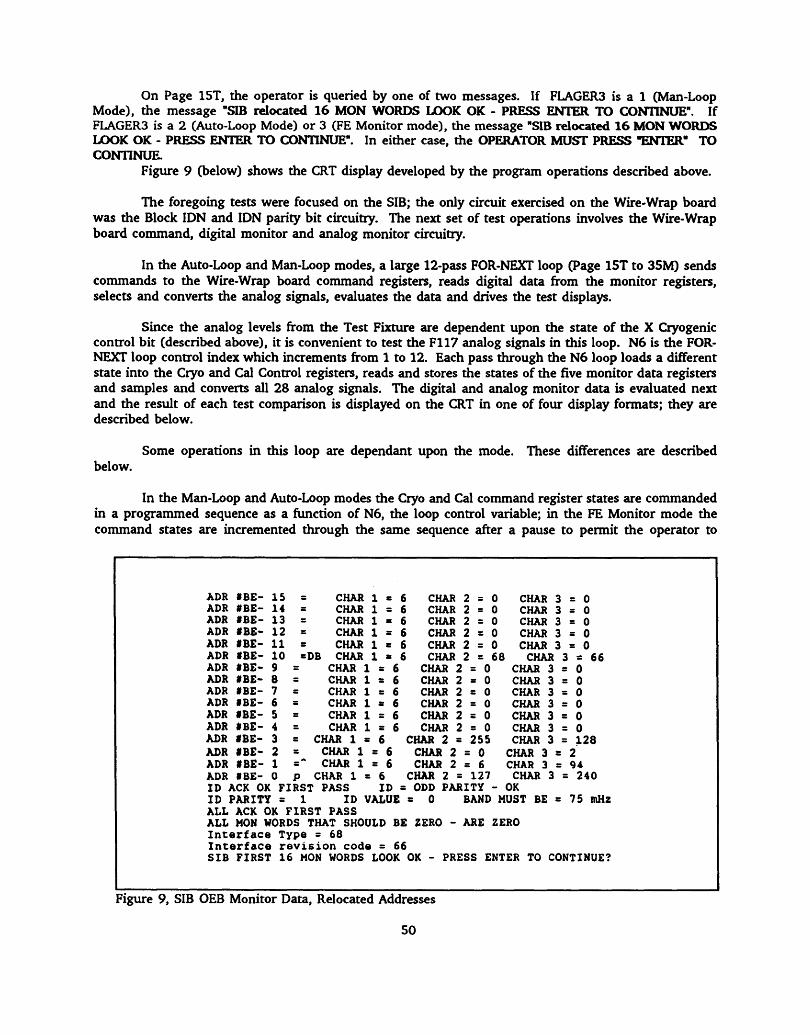
On Page 15T, the operator is queried by one of two messages. If FLAGER3 is a 1 (Man-Loop Mode), the message "SIB relocated 16 MON WORDS LOOK OK - PRESS ENTER TO CONTINUE". If FLAGER3 is a 2 (Auto-Loop Mode) or 3 (FE Monitor mode), the message "SIB relocated 16 MON WORDS LOOK OK - PRESS ENTER TO CONTINUE". In either case, the OPERATOR MUST PRESS "ENTER" TO CONTINUE.
Figure 9 (below) shows the CRT display developed by the program operations described above.
The foregoing tests were focused on the SIB; the only circuit exercised on the Wire-Wrap board was the Block IDN and IDN parity bit circuitry. The next set of test operations involves the Wire-Wrap board command, digital monitor and analog monitor circuitry.
In the Auto-Loop and Man-Loop modes, a large 12-pass FOR-NEXT loop (Page 15T to 35M) sends commands to the Wire-Wrap board command registers, reads digital data from the monitor registers, selects and converts the analog signals, evaluates the data and drives the test displays.
Since the analog levels from the Test Fixture are dependent upon the state of the X Cryogenic control bit (described above), it is convenient to test the F117 analog signals in this loop. N6 is the FOR- NEXT loop control index which increments from 1 to 12. Each pass through die N6 loop loads a different state into the Cryo and Cal Control registers, reads and stores the states of the five monitor data registers and samples and converts all 28 analog signals. The digital and analog monitor data is evaluated next and the result of each test comparison is displayed on the CRT in one of four display formats; they are described below.
Some operations in this loop are dependant upon the mode. These differences are described below.
In the Man-Loop and Auto-Loop modes the Cryo and Cal command register states are commanded in a programmed sequence as a function of N6, the loop control variable; in the FE Monitor mode the command states are incremented through the same sequence after a pause to permit the operator to
ADR iBE- 15 = CHAR 1=6 CHAR 2=0 CHAR 3=0 ADR #BE- 14 = CHAR 1=6 CHAR 2=0 CHAR 3=0 ADR #BE- 13 = CHAR 1=6 CHAR 2=0 CHAR 3=0 ADR iBE- 12 = CHAR 1=6 CHAR 2=0 CHAR 3=0 ADR »BE- 11 = CHAR 1=6 CHAR 2=0 CHAR 3=0 ADR fBE- 10 =DB CHAR 1=6 CHAR 2 = 68 CHAR 3 = 66 ADR #BE- 9 = CHAR 1=6 CHAR 2=0 CHAR 3=0 ADR IBE- 8 = CHAR 1=6 CHAR 2=0 CHAR 3=0 ADR #BE- 7 = CHAR 1=6 CHAR 2=0 CHAR 3=0 ADR fBE- 6 = CHAR 1=6 CHAR 2=0 CHAR 3=0 ADR iBE- 5 = CHAR 1 = 6 CHAR 2 = 0 CHAR 3 = 0 ADR #BE- 4 = CHAR 1=6 CHAR 2=0 CHAR 3=0 ADR #BE- 3 = CHAR 1 = 6 CHAR 2 = 255 CHAR 3 = 128 ADR #BE- 2 = CHAR 1=6 CHAR 2=0 CHAR 3=2 ADR »BE- 1 =~ CHAR 1=6 CHAR 2=6 CHAR 3 = 94 ADR fBE- 0 p CHAR 1=6 CHAR 2 = 127 CHAR 3 = 240 ID ACK OK FIRST PASS ID = ODD PARITY - OK ID PARITY =1 ID VALUE = 0 BAND MUST BE = 75 mHz ALL ACK OK FIRST PASS ALL MON WORDS THAT SHOULD BE ZERO - ARE ZERO Interface Type = 68 Interface revision code = 66 SIB FIRST 16 MON WORDS LOOK OK - PRESS ENTER TO CONTINUE?
Figure 9, SIB OEB Monitor Data, Relocated Addresses
50
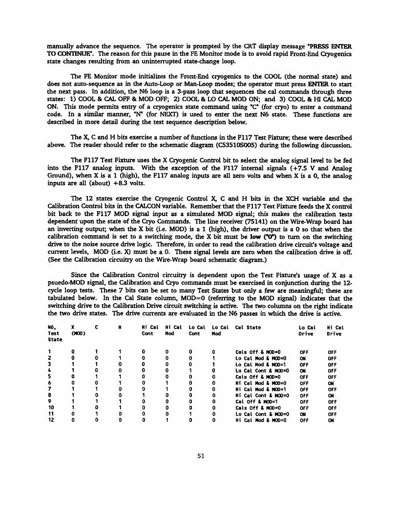
manually advance the sequence. The operator is prompted by the CRT display message "PRESS ENTER TO CONTINUE". The reason for this pause in the FE Monitor mode is to avoid rapid Front-End Cryogenics state changes resulting from an uninterrupted state-change loop.
The FE Monitor mode initializes the Front-End cryogenics to the COOL (the normal state) and does not auto-sequence as in the Auto-Loop or Man-Loop modes; the operator must press ENTER to start the next pass. In addition, the N6 loop is a 3-pass loop that sequences the cal commands through three states: 1) COOL & CAL OFF & MOD OFF; 2) COOL & LO CAL MOD ON; and 3) COOL & HI CAL MOD ON. This mode permits entry of a cryogenics state command using "C" (for cryo) to enter a command code. In a similar manner, "N" (for NEXT) is used to enter the next N6 state. These functions are described in more detail during the test sequence description below.
The X, C and H bits exercise a number of functions in die F117 Test Fixture; these were described above. The reader should refer to the schematic diagram (C53510S005) during the following discussion.
The F117 Test Fixture uses the X Cryogenic Control bit to select the analog signal level to be fed into the F117 analog inputs. With the exception of the F117 internal signals (+7.5 V and Analog Ground), when X is a 1 (high), the F117 analog inputs are all zero volts and when X is a 0, the analog inputs are all (about) +8.3 volts.
The 12 states exercise the Cryogenic Control X, C and H bits in the XCH variable and the Calibration Control bits in the CALCON variable. Remember that the F117 Test Fixture feeds the X control bit back to the F117 MOD signal input as a simulated MOD signal; this makes the calibration tests dependent upon the state of the Cryo Commands. The line receiver (75141) on the Wire-Wrap board has an inverting output; when the X bit (i.e. MOD) is a 1 (high), the driver output is a 0 so that when the calibration command is set to a switching mode, the X bit must be low ("CT) to turn on the switching drive to the noise source drive logic. Therefore, in order to read the calibration drive circuit's voltage and current levels, MOD (i.e. X) must be a 0. These signal levels are zero when the calibration drive is off. (See the Calibration circuitry on the Wire-Wrap board schematic diagram.)
Since the Calibration Control circuitry is dependent upon the Test Fixture's usage of X as a psuedo-MOD signal, the Calibration and Cryo commands must be exercised in conjunction during the 12- cyde loop tests. These 7 bits can be set to many Test States but only a few are meaningful; these are tabulated below. In the Cal State column, MOD=0 (referring to the MOD signal) indicates that the switching drive to the Calibration Drive circuit switching is active. The two columns on die right indicate the two drive states. The drive currents are evaluated in the N6 passes in which the drive is active.
N6, X c H Hi Cal Hi Cal Lo Cal Lo Cal Cal State Lo Cal Hi Cal Test (MOD) Cont Mod Cont Mod Drive Drive State
1 0 0 0 0 0 Cals Off & M00=0 OFF OFF 2 0 0 0 0 0 1 Lo Cal Mod & MOD=0 ON OFF 3 1 0 0 0 1 Lo Cal Mod & M00=1 OFF OFF 4 1 0 0 0 1 0 Lo Cal Cont & MOD=0 ON OFF 5 0 0 0 0 0 Cals Off & M00=0 OFF OFF 6 0 0 0 1 0 0 Hi Cal Mod & MOD=0 OFF ON 7 1 0 0 1 0 0 Hi Cal Mod & M0D=1 OFF OFF 8 1 0 0 1 0 0 0 Hi Cal Cont & M00=0 OFF ON 9 1 0 0 0 0 Cal Off & M0D=1 OFF OFF 10 1 0 0 0 0 0 Cals Off & M00=0 OFF OFF 11 0 0 0 0 1 0 Lo Cal Cont & MOD=0 ON OFF
51
To test the PUT'S Front-End Cryo monitor discretes inputs, the Test Fixture routes the X, C and H Cryogenic Control bits to the X Mon, C Mon and H Mon pins on Jl; therefore these monitor bits should always reflect the state of the command bits. In the following discussion X, C and H designates these three control bits; if the X Mon, C Mon and H Mon bits are referenced, they will have this designation.
The Test Fixture jumpers the F117 multiplex address bits ADDRO, ADDR1 and ADDR2 to the Front-End's control logic output discretes: M - Manual Mode monitor, P - Pump Request, and S - Solenoid state, respectivley. These multiplex address bits cycle the three discretes through 8 states.
When a fault condition is detected in the Auto-Loop mode, FLAGER3 is forced to 1, the Man- Loop mode. This transition enables the operator to make adjustments or measurements. After this transition, program execution continues in the the Man-Loop mode when resumed by the operator; it is not possible to return to the Auto-Loop mode during the balance of the program execution. There are no transitions between FE Monitor mode and the other two modes.
During die digital monitor portion of the loop (Page 16T), the states of the five (addresses H20, .. H24) F117 Monitor Data registers are loaded into the DIGCHAR$ array. The MONCHARS array is defined by the DIM MONCHARS (&H24, 3, 16) statement on Page IT. The &H24 dimension is 36D. During each N6 pass, die array is loaded with 3 bytes x 5 addresses (ACK, MDH and MDL for H20,... H24) or 15 bytes/pass. Thus, the 12 N6 passes load 180 bytes into the array.
In the digital command portion of the loop (Page 15T), the Cryo and Calibration command registers will be set to one of 12 sets of states. The readout of the associated digital monitor registers (addresses H20 and H22) should match the command register states. The contents of the address 23H register (Band Code, Mod Level, and Front-End Serial Number) should reflect the state set by the Test Fixture logic circuits and the X, C and H Cryo command bits. These states are tabulated in the preceding description of the Test Fixture. X Mon, C Mon, H Mon in the Front-End discretes monitor register (address 21H) should be identical to the X, C and H Cryogenic Control bits and discretes M, P and S should reflect the states of the ADDRO, ADDR1 and ADDR2 multiplex address bits. The F117 module Serial Number readout should be the value hard-wired on the Wire-Wrap connector pins.
In the FE Monitor mode, the Front-End's cryogenic state monitor bits (X Mon, C Mon and H Mon from address H20) reflect the state of the Front-End's cryogenic control logic. If the Front-End's manual control switch is in any position other than Computer, the F117 Test System cannot change the Front- End's cryogenic state. If the switch is in the Computer position, the cryogenic state will be controlled by the F117 Test System. Secondly, in this mode the Front-End's M, P and S discrete bits are controlled by the Front-End control logic and reflect die state of this logic, not the test program's commands or states. Finally, in the FE Monitor mode, the ANLG3 inputs on Jl are floating and can assume any value. The Jl pins assigned to ANLG3 are not connected in the Front-End; the ANLG3 analog values in this mode are the result of minute leakage currents driving the A/D's high input impedance. The leakage currents are mulitplexer leakage currents and bias currents in the A/D converter's input amplifier.
The acquistion and storage of analog monitor data is not dependent upon mode but the evaluation (described below) is. The analog data is stored in the ANLGCHARS array which is defined by the DIM ANLGCHAR$(&H1F, 3, 16) statement on Page IT. The first 12 x 16 x 3 sets of locations are cleared to O's (Page 17T).
The address range of the analog data is 28D (1FH minus 3H) which covers all analog addresses. This includes the 8 external multiplexer (ANLG3) addresses (18H - 1FH). The analog data addresses were tabulated in Sections 1 and 2 above. During each pass of the N6 loop, 28 analog values for this address range are read and stored in the ANLGCHARS array. The first address assigned to the F117-Front-End set is 4H for the Low Cal Current and the last is 17H for the Dewar Vacuum. The Test Fixture connects the
52
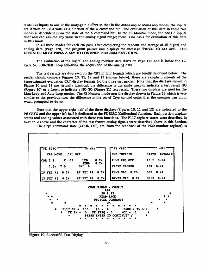
8 ANLG3 inputs to one of the unity-gain buffers so that in the Auto-Loop or Man-Loop modes, the inputs are 0 volts or +8.3 volts as a function of the X command bit. The evaluation of this data in these two modes is dependent upon the state of the X command bit. In the FE Monitor mode, the ANLG3 inputs float and can assume any value in the analog signal range; there is no basis for evaluation of this data in this mode.
In all three modes for each N6 pass, after completing the readout and storage of all digital and analog data (Page 17B), the program pauses and displays the message "PRESS TO GO ON". THE OPERATOR MUST PRESS A KEY TO CONTINUE PROGRAM EXECUTION.
The evaluation of the digital and analog monitor data starts on Page 17B and is inside the 12- cycle N6 FOR-NEXT loop following the acquisition of the analog data.
The test results are displayed on the CRT in four formats which are briefly described below. The reader should compare Figures 10, 11, 12 and 13 (shown below); these are sample print-outs of the (approximate) evaluation CRT display formats for the three test modes. Note that the displays shown in Figure 10 and 11 are virtually identical; the difference is the smile used to indicate a test result GO (Figure 10) or a frown to indicate a NO GO (Figure 11) test result. These two displays are used for the Man-Loop and Auto-Loop modes. The FE Monitor mode uses the display shown in Figure 13 which is very similar to the previous two; the difference is the set of Cryo control codes that the operator can input when prompted to do so.
Note that the upper right half of the three displays (Figures 10, 11 and 12) are dedicated to the FE CRYO and the upper left half is dedicated to the FE ELEC (Calibration) function. Each portion displays states and analog values associated with these two functions. The F117 register states were described in Section 2 above and the character of the test fixture analog signals were described above in this Section.
The Cryo command state (COOL, OFF, etc. from the readback of the H20 monitor register) is
CAL MODE CAL OFF
CAL I 1 V .02
7.5V 7.5
LED 8.24 SENS 8.24
GND 0
LF FET fl 8.24 RT FET fl 8.24
—FE CRYO——
CMD INVALID STATE INVALID
PUMP REQ OFF AC I 8.24
VALVE CLOSED 15K 8.24
IPUMP VAC 8.25 50K 8.24
COMPUT/MAN * COMPUT ADR
< 20 & 22 * * READ-BACK • * DIGITAL COMMANDS * * OK
*********** * F117 SN = 100 ID = 0 BAND = 75 mHz
* FE SN * 0 FE FREQ * 0 MOD « 0 * * PRESS ENTER TO CONTINUE? [ *
***********
* * *
*
Figure 10, Successful Test Display
53

displayed adjacent to the CMD label. The Front-End cryo response state read from the H21 register (e.g. COOL, STRESS, etc. from X Mon, C Mon and H MON) is displayed adjacent to the STATE label. The state of two other discretes, P and S, are displayed with the labels and states PUMP REQ OFF (or ON) and VALVE OPEN (or CLOSED) displayed below the mode states. Analog values also displayed in this field are a function of the N6 loop index and should be either 0 volts or about +8.3 volts (if not erroneous).
Calibration command state (e.g. LO CAL SW, etc.) read from the H22 monitor register is displayed adjacent to the CAL MODE label. The associated analog values of calibration current and voltage are displayed below the mode states. These values are a function of the N6 loop index value and should be either 0 volts or about +8.3 volts.
The fourth display is used only in the Manual-Loop and FE Monitor modes. The analog data is a tabular display of hex addresses and values. Note that the ANLG3 data is displayed; it is not included in the other three displays. The digital data is labeled by a functional label (e.g. CAL) and the hex address. The data is presented as decimal and binary 8-bit values (remember that the H20, H12, H22 and H24 monitor data registers are 8 bit registers). ID1 and ID2 values are the two halves of the 16-bit, H23 register's Front-End Band Code, Mod Code and Serial Number. The top line indicates test conditions. The TEST STATE label indicates the N6 loop index value (tabulated above); ANALOG indicates the 0 or +8.3 volts analog stimulus value; MOD shows the state of the MOD bit and noise source drive currents; the EVEN BITS = (1 or 0) and ODD BITS = (0 or 1) indicates the states of the four calibration control bits.
The text below does not describe how the formats are generated or the display color assignments (the text is monochrome). The reader should note that Figures 10, 11 and 12 are not exact replicas of the actual CRT displays; the difference is small and is the result of the printer's response to the CRTs display code values. These displays were obtained by using the computer's "Print Screen" key; the program does not print a hard copy of the data evaluation.
During each pass through the data evaluation portion of the program, the data values are related to the conditions under which they were stored (tabulated above); these conditions are the basis for the GO/NO-GO evaluation. In the Man-Loop and Auto-Loop modes during die data evaluation, an error flag
CAL MODE LO CAL SW 1
CAL I 3 V 27
7.5V 7.5
.4 LED 8.13 SENS 8.2
GND 0
LF FET #1 6.03 RT FET #1 7.89
-FE CRYO —
CMD PUMP STATE COOL
PUMP REQ ON AC I 8
VALVE OPEN 15K 7.99
PUMP VAC 6. 04 50K 8.01
* *ft
COMPUT/MAN = COMPUT ADR
20 A 22 READ-BACK
DIGITAL COMMANDS OK
*************** F117 SN = 100 ID » 0 BAND = 75 mHz * FE SN « 0 FE FREQ = 0 MOD = 0 *
PRESS ENTER TO CONTINUE? [ i*****************
Figure 11, Failed Test Display
54
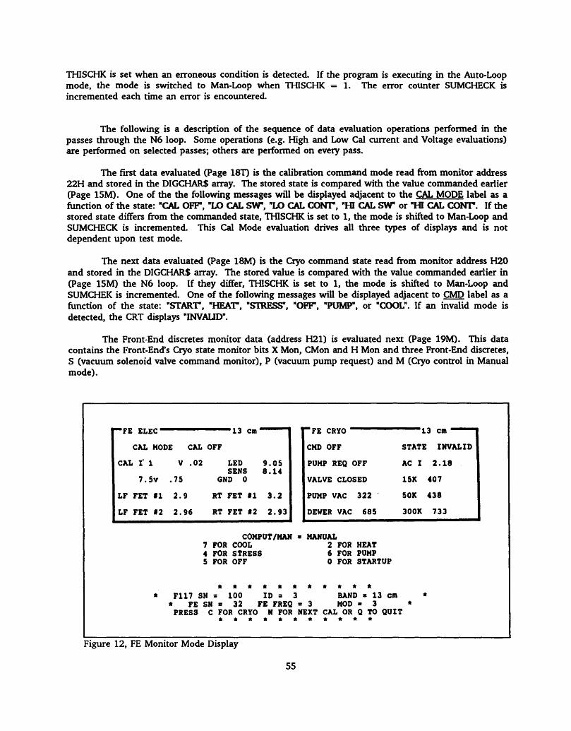
THISCHK is set when an erroneous condition is detected. If the program is executing in the Auto-Loop mode, the mode is switched to Man-Loop when THISCHK = 1. The error counter SUMCHECK is incremented each time an error is encountered.
The following is a description of the sequence of data evaluation operations performed in the passes through the N6 loop. Some operations (e.g. High and Low Cal current and Voltage evaluations) are performed on selected passes; others are performed on every pass.
The first data evaluated (Page 18T) is the calibration command mode read from monitor address 22H and stored in the DIGCHARS array. The stored state is compared with the value commanded earlier (Page 15M). One of the the following messages will be displayed adjacent to the CAL MODE label as a function of the state: "CAL OFF, "LO CAL SW", "LO CAL CONT, "HI CAL SW" or "HI CAL CONT. If the stored state differs from the commanded state, THISCHK is set to 1, the mode is shifted to Man-Loop and SUMCHECK is incremented. This Cal Mode evaluation drives all three types of displays and is not dependent upon test mode.
The next data evaluated (Page 18M) is the Cryo command state read from monitor address H20 and stored in the DIGCHARS array. The stored value is compared with the value commanded earlier in (Page 15M) the N6 loop. If they differ, THISCHK is set to 1, the mode is shifted to Man-Loop and SUMCHEK is incremented. One of the following messages will be displayed adjacent to CMD label as a function of the state: "START, "HEAT, "STRESS", "OFF, "PUMP", or "COOL". If an invalid mode is detected, the CRT displays "INVALID".
The Front-End discretes monitor data (address H21) is evaluated next (Page 19M). This data contains the Front-End's Cryo state monitor bits X Mon, CMon and H Mon and three Front-End discretes, S (vacuum solenoid valve command monitor), P (vacuum pump request) and M (Cryo control in Manual mode).
CAL MODE CAL OFF CMD OFF STATE INVALID 1
CAL 11 V .02 LED 9.05 SENS 8.14
7.5v .75 GND 0
PUMP REQ OFF AC I 2.18
VALVE CLOSED 15K 407
LF FET #1 2.9 RT FET #1 3.2 PUMP VAC 322 50K 438
LF FET #2 2.96 RT FET 92 2.93 DEWER VAC 685 300K 733
COMPUT/MA) 7 FOR COOL 4 FOR STRESS 5 FOR OFF
t * MANUAL 2 FOR HEAT 6 FOR PUMP 0 FOR STARTUP
***********
Figure 12, FE Monitor Mode Display
55

The Front-End's cryo state (X Mon, C Mon and H Mon) is evaluated and one of the following messages is displayed adjacent to the STATE label: "START, "HEAT, "STRESS", "OFF, "PUMP", or "COOL". If an invalid mode is detected, the CRT displays "INVALID".
The Front-End's S, P and M discretes are generated by the Front-End control logic. One of the text messages "OPEN or CLOSED", "ON or OFF will be displayed adjacent to the VALVE and PUMP REQ labels, respectively, to indicate the state of these discrete bits (Page 19M). The M bit indicates the state of the Front-End's cryogenic mode control switch. Either a "MANUAL" or "COMPUT message will be displayed adjacent to die COMPUT/MAN label as a function of this switch position.
If the program is executing in the Auto-Loop or Man-Loop modes, the test fixture's simulated values are read from H21. Remember that X Mon, C Mon and H Mon follow the cryogenic control bits X, C and H. If an error is detected, THISCHK is set to 1 (forcing a transition to the Man-Loop mode) and incrementing SUMCHECK.
When the program is executing in the Auto-Loop or Man-Loop mode with the F117 Test Fixture, these discretes are determined by the fixture circuitry that connects these bits to the three lower mux address bits. In these two modes, the Front-End S, P and M discretes data is determined by the state of mux address H21 (binary 0010 0001). Since S, P and M follow the address bits, then S = 0 (Addr2), P = 0 (Addrl) and M = 1 (AddrO); any other state is an error in the Auto-Loop or Man-Loop mode.
In the Auto-Loop and Man-Loop modes, Low and High Calibration currents through the two 1000 Ohm resistors in the Test Fixture are evaluated next (Page 20T). As noted in the calibration states table above, the Low Calibration drive is on during N6 passes 2 and 11; the High Calibration drive is on during passes 6 and 12. The drive currents and voltages are evaluated on these passes. The calibration drive values (in mA) are displayed adjacent to the CAL I label. The Calibration current data display is identical for all three program modes. If the drive current exceeds +/- 50 mA in any pass, THISCHK is set to 1, SUMCHECK is incremented and the program execution mode is set to Man-Loop. The data display is
TEST STATE 3 ANALOG s 0 V MOD = OFF/I EVEN BITS = 1 ODD BITS = 0
ADR 4 .03 ma ADR 10 6.03 V ADR 5 0 ma ADR 11 7.89 V ADR 18 4.02 V ADR 6 27.4 V ADR 12 8.01 V ADR 19 4.02 V ADR 7 0 V ADR 13 8.01 V ADR 1A 4.02 V ADR 8 6.04 V ADR 14 7.99 K ADR IB 4.02 V ADR 9 8 A ADR 15 8.01 K ADR 1C 4 V ADR A 8.13 V ADR 16 8.01 K ADR ID 4 V ADR B 8.2 V ADR 17 7.96 V ADR IF 4 V ADR C 7.5 V ADR D 0 V
CMD MONIT WORD &H20 — 6 0 0 0 0 0 1 1 0 CAL MONIT WORD &H21 s 255 1 1 1 1 1 1 1 1 STATE MONIT WORD &H22 r 1 0 0 0 0 0 0 0 1 ID1 MONIT WORD &H23 s 255 1 1 1 1 1 1 1 1 ID2 MONIT WORD &H23 s 255 1 1 1 1 1 1 1 1 FE MONIT WORD &H24 s 100 0 1 1 0 0 1 0 0
13, Backup Display
56
identical for all three modes of program execution.
Low and High Calibration voltages across the 1000 Ohm resistors or Front-End's noise sources (scaled to 28 volts) are displayed adjacent to the V label (Page 20M). If the drive voltage is less than +27 volts or greater than +28.5 volts in the N6 passes when the drive is on or exceeds +/- 0.50 volts in the N6 passes when the drive is off, THISCHK is set to 1, SUMCHECK is incremented and the program execution mode is set to Man-Loop. The data display is identical for all three modes of program execution and is displayed adjacent to the V label.
The LED drive voltage is evaluated next (Page 2IT). The data value is displayed adjacent to the LED label. A subroutine CHECKUM is called to evaluate this data; from this point on, CHECKUM is frequendy called for evaluations of analog data. CHECKUM uses fixed limits of +/- 25 mV and +8.0 to +8.5 V as a function of the N6 index value. CHECKUM sets THISCHK = 1 and increments SUMCHECK for values outside these limits.
The SENS voltage is evaluated next (Page 21M). CHECKUM is called to evaluate the data. The data value is displayed adjacent to the SENS label.
The Front-End's AC current load monitor voltage (ACI) is evaluated next (Page 21B). CHECKUM is called to evaluate the data. The data value is displayed adjacent to the AC I label.
The PUT'S +7.5 volt reference voltage is evaluated next (Page 22T). CHECKUM is called to evaluate the data. The data value is displayed adjacent to the 7.5 V label. If the program is operating in the FE Monitor mode, the value printed is 1/10 the measured value.
The analog ground voltage is evaluated next (Page 22M). Since it is an F117 internal function, it has a constant value and is therefore independent of the N6 value. The tolerance range for this signal is +/- 0.25 volts and it is tested on all passes through the 12-cycle loop. The value is displayed adjacent to the GND label and is not dependent upon die program execution mode. When it is outside this tolerance range, THISCHK is set to 1, SUMCHECK is incremented and the program execution mode is set to Man-Loop. In the FE Monitor mode the value printed is 1/10 the measured value.
The 15K voltage is evaluated next (Page 22B). CHECKUM is called to evaluate the data. The value is printed adjacent to the 15K label. In the FE Monitor mode the value printed is 100 times the measured value.
The LF FET #1 voltage is evaluated next (Page 23T). CHECKUM is called to evaluate the data. The value is printed adjacent to the LF FET #1 label.
The RT FET #1 voltage is evaluated next (Page 23M). CHECKUM is called to evaluate the data. The value is printed adjacent to the RT FET #1 label.
The PUMP VAC is evaluated next (Page 23B). CHECKUM is called to evaluate the data. The value is printed adjacent to the PUMP VAC label. In the FE Monitor mode the value printed is 100 times the measured value.
The 50K voltage is evaluated next (Page 24T). CHECKUM is called to evaluate the data. The value is printed adjacent to the 50K label. In the FE Monitor mode the value printed is 100 times the measured value.
The LF FET #2 voltage is evaluated next (Page 24M). CHECKUM is called to evaluate the data. The value is printed adjacent to the LF FET #2 label.
57
The RT FET #2 voltage is evaluated next (Page 24B). CHECKUM is called to evaluate the data. The value is printed adjacent to the RT FET #2 label.
The DEWER VAC voltage is evaluated next (Page 25T). CHECKUM is called to evaluate the data, the value is printed adjacent to the DEWER VAC label. In the FE Monitor mode the value printed is 100 times the measured value.
The 300K voltage is evaluated next (Page 25M). CHECKUM is called to evaluate the data. The value is printed adjacent to the 300K label. In the FE Monitor mode the value printed is 100 times the measured value.
The Band Code, Front-End Serial Number and Mod level codes are extracted from H23 (Page 25M) for printout (described below).
The eight ANLG3 external multiplexer voltages are evaluated next (Page 26T). The values are loaded into the ANVAL array and evaluated by CHECKUM. If outside the CHECKUM tolerances, the message "BAD AUX ANALOG" is displayed. In the Man-Loop and Auto-Loop modes, the ANLG3 lines are driven by the Test Fixture's 0 and +8.3 signals. In the FE Monitor mode the ANLG3 lines float.
The operations described above are the data evaluation and display functions. The next steps in program execution are the final test decisions and generation of the GO (smile) or NOGO (frown) display symbols.
In the Man-Loop and Auto-Loop modes, a final summary message "ADR 20 & 22 READ BACK DIGITAL COMMANDS OK" is displayed (Page 27) for either case of SUMCHECK (either 0 or not 0).
Enclosed within the smile or frown, the Figures 10, 11 and 12 displays show the IDN and the H23-H24 monitor data values displayed adjacent to the following labels: F117 SN = (serial number), ID = (ID value), BAND = (band name), FE SN = (serial number), FE FREQ = (band code), MOD = (mod level). These display values are followed by the prompt: "PRESS ENTER TO CONTINUE".
In the FE Monitor mode, the display shows a set of Cryo control codes and a prompt "PRESS C FOR CRYO N FOR NEXT CAL OR Q TO QUIT. If the operator presses C, he may enter any of the displayed codes to command the associated cryo modes. If die operator presses N, the next FE Monitor cal state (e.g. CAL OFF, LO CAL and HI CAL) in the N6 sequence is commanded and control reverts to the start of the N6 loop (Page 15T). If he presses Q, the Backup display (Figure 13, described above) is entered. This display is also entered in the Man-Loop mode after completing the "PRESS ENTER TO CONTINUE" response of the previous paragraph.
In the FE Monitor mode, after displaying the Backup display (Page 35), the prompt "PRESS ENTER TO CONTINUE" ends the program execution when the operator presses ENTER. This prompt is also displayed in the Man-Loop and Auto-Loop modes; when the operator responds by pressing ENTER, the flag GONO is set to the SUMCHECK value. If GONO is 0, the message "F117 PASSED PASSED TESTING" and the F117 serial number is printed adjacent to the F117 SN = label. If GONO is not 0, the message "F117 FAILED TESTING" and the F117 serial number is printed adjacent to the F117 SN label.
This final ENTER response ends program execution.
Alignment Adjustments
The SIB alignment should be done in the Maxtester system; the F117 module is not an adequate test environment for this board. SIB features that are not testable in the F117 test environment are the
58
CDH output on the upper byte of the CMD/MON bus, the two upper address bits and the SIB state LED drive circuitry. Secondly, the F117 analog circuitry does not provide adequate negative and positive reference voltages for a comprehensive SIB analog alignment and the ANLG-0 input is not testable.
The only alignment adjustments on the Wire-Wrap board are the calibration current monitor zero- adjustment potentiometers, R55 and R56. To adjust these two potentiometers, use a test fixture that approximately simulates a Front-End (i.e. an IDN code, etc.). The test fixture should have two 1000 Ohm resistors to simulate noise source loads with manual switches (or clip leads, etc.) to connect or disconnect the two loads. In the FE Monitor mode, set die calibration drives active (i.e. the calibration drive outputs at +28 volts). With die loads disconnected, adjust the two potentiometers for zero volt outputs on amplifiers 3DA-1 and 3DA-7. Connect the two loads by actuating the switches; the amplifier outputs should be + 0.280 volts since the amplifier scaling is 100 mA/volt.
59

60
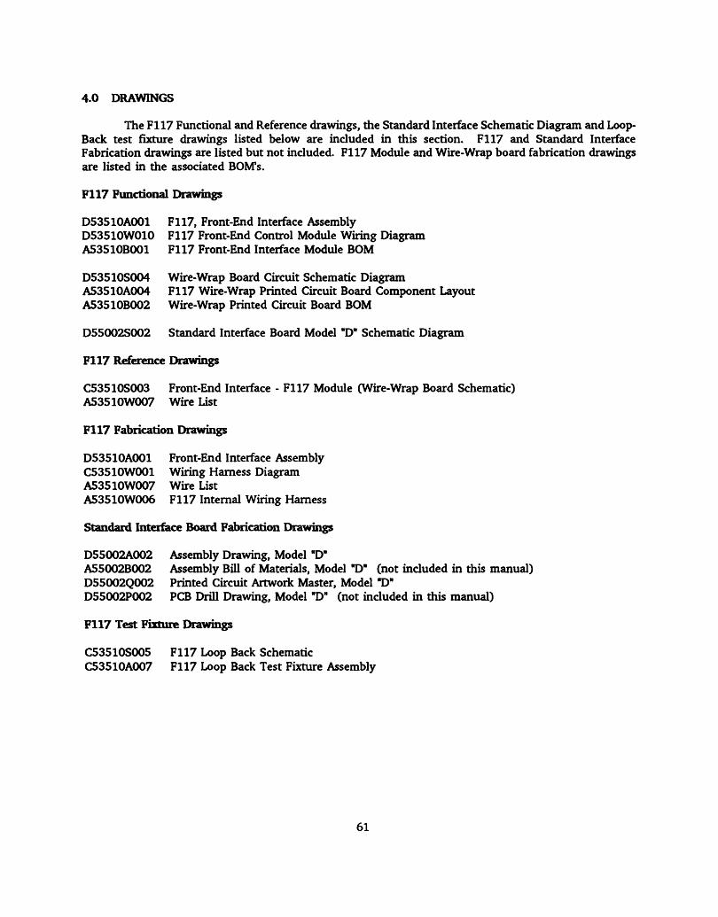
4.0 DRAWINGS
The F117 Functional and Reference drawings, the Standard Interface Schematic Diagram and Loop- Back test fixture drawings listed below are included in this section. F117 and Standard Interface Fabrication drawings are listed but not included. F117 Module and Wire-Wrap board fabrication drawings are listed in the associated BOM'S.
F117 Functional Drawings
D53510A001 F117, Front-End Interface Assembly D53510W010 F117 Front-End Control Module Wiring Diagram A53510B001 F117 Front-End Interface Module BOM
D53510S004 Wire-Wrap Board Circuit Schematic Diagram A53510A004 F117 Wire-Wrap Printed Circuit Board Component Layout A53510B002 Wire-Wrap Printed Circuit Board BOM
D55002S002 Standard Interface Board Model "D" Schematic Diagram
F117 Reference Drawings
C53510S003 Front-End Interface - F117 Module (Wire-Wrap Board Schematic) A53510W007 Wire List
F117 Fabrication Drawings
D53510A001 Front-End Interface Assembly C53510W001 Wiring Harness Diagram A53510W007 Wire List A53510W006 F117 Internal Wiring Harness
Standard Interface Board Fabrication Drawings
D55002A002 Assembly Drawing, Model "D" A55002B002 Assembly Bill of Materials, Model "D" (not included in this manual) D55002Q002 Printed Circuit Artwork Master, Model "D" D55002P002 PCB Drill Drawing, Model "D" (not included in this manual)
F117 Test Fixture Drawings
C53510S005 F117 Loop Back Schematic C53510A007 F117 Loop Back Test Fixture Assembly
61

62
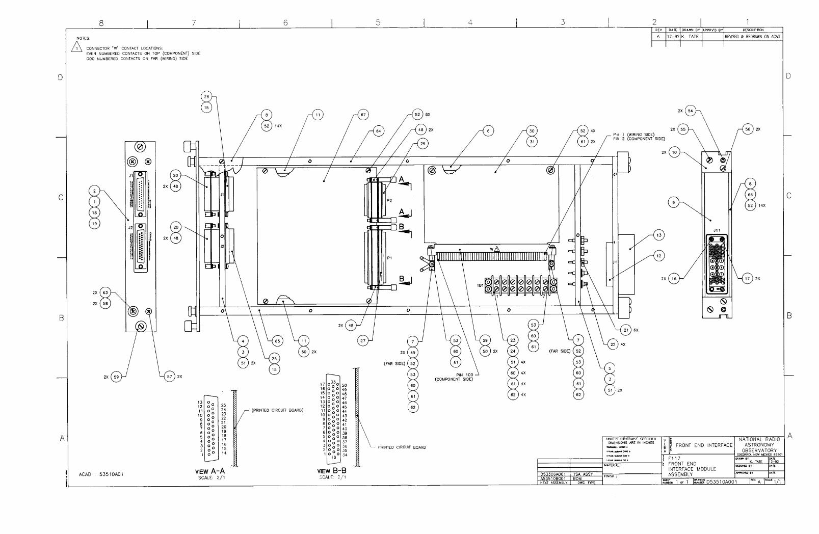
8 5 3
NOTES:
CONNECTOR "W" CONTACT LOCATIONS:
EVEN NUMBERED CONTACTS ON TOP (COMPONENT) SIDE
ODD NUMBERED CONTACTS ON FAR (WIRING) SIDE
2-92 K. TATE REVISED 4 REDRAWN ON ACAD
D
C
B
A
ACAD : 53510A01 VIEW A-A SCALE: 2/1
VIEW B-B SCALE: 2/1
D53306A001 A53510B001 NEXT ASSEMBLY
1SA ASSY BOM
DWG. TYPE
UNLEiS OTHERWISE SPECIFIED DIMENSIONS ARE IN INCHES
t HM* 'CCWU (JCt) *
D
C
B
FRONT END INTERFACE
F117 i FRONT END
INTERFACE MODULE ASSEMBLY
SHEET . . NUMBER I OF I
NATIONAL RADIO ASTRONOMY
OBSERVATORY SOCORRO, NEW MEXICO 67601
DESIGNED BY
APPROVED BY
ISKSf D53510A001 |SCALE 1A
A

5 4
r
D
X.
JII-io ro
FT3
FT4
■I- J11-29 ns
J11-9 RED_ FTS
4^-
^^
^
RFI ENCLOSURE
7 5 .WW BOARD +5. ±15, +2aV
P2
RED
■V 15 16 1* 13 ■
! JLl-f +15V -15V +5V DIG T GND
P2pr_i ■Jr J 34 50
BU<_ mo
c
■-TW "=" PR I
Jll-14 WHTfjy
M & C BUS SIGNALS
PR | /
B
NOT USED
DIG +5V GND hi
STANDARD INTERFACE BOARD VERSION "D"
SYSRST+
SYSRST-
RSTSW
DIG GND
PI.7
P1.6
XACT
DOUT
PARK
BUSY
MSG
DIG GND
+5V
ANALOG GND
ASSEMBLY: SCHEMATIC:
D55002A0O2 D55001S002
ANLG 2+
ANLG 1 +
ANLG 4+
ANLG 5+
ANLG 6+
ANLG 7+
ANLG 1-
ANLG 2-
ANLG 4-
ANLG 5-
ANLG 6-
ANLG 7-
ANLG GND
C/M 0
C/M 1
C/M 2
C/M 3
C/M 4
C/M 5
C/M 6
C/M 7
C/M 8
C/M 9
C/M 10
C/M 11
C/M 12
C/M 13
C/M 14
C/M 15
.T ANALOG MUX SIGNALS
4y ANALOG MUX SIGNALS -r
/ 7^
TRI-STATE CMD/MON BUS
V^T rK'T''' 1 ANLG 0+
18 ANLG 0-
V 'T ADDRO
ADDR1
ADDR2
ADDR3
ADDR4
ADDR5
ADDR6
ADDR7
ANLG3+
ANLG3-
R/W(L)
REV REQ
ocy ACK
ANEN B
H/L(L)SEL
A M0DJ^11 ~-™. L.
>■
ADDRESS BUS
NOT USIED
NOT USIED
T T I I
l_. ACAD : 5351 OW10
—r— DEVICE
CONTROL
y
-K 100 94 95 96 h-
y
REF +5V +5V -15V +15V+28V GND
ANLG1+. ANLG2+ PA(L)
F3
ANLG 4+ F2
ANLG 5+ Fl
ANLG 6+ FO
ANLG 7+ S5
S4
S3
S2
SI
"XT
35 C/M 0
36 C/M 1
37 C/M 2
38 C/M 3
39 C/M 4
40 C/M 5
41 C/M 6
42 C/M 7
43 C/M 8
44 C/M 9
45 C/M 10
46 C/M 11
47 C/M 12
48 C/M 13
51 C/M 14
WIRE-WRAP CIRCUIT BOARD
ASSEMBLY: D53540A004 SCHEMATIC: C53510S003 SCHEMATIC: D53510S004
29 ADDRO
30 ADDR1
31 ADDR2
32 ADOR3
33 ADDR4
Ml
MO
CAL
HI CAL
H(L)
VD
15K
50K
300K
ACI
RFI
RF2
LF1
LF2
LED(L)
0 GND
SENS
M(L)
X MON
C MON
H MON(L)
" 17 H/L(L)
- 93 MOD
■ ^TTSNO
R/wfL) REV REQ
DEV ACK
ANEN B
H/L(L)SEL
MOD
SNO SN1 SN2 SN3 SN4
IT zr j
BAND l/D CODE
7" RCVR SERIAL
NUMBER CODE
4* RCVR MOD CODE
/"CAL DRIVE
/■ CRYO CMD
r- SN5 SN6 SN7 GND +5V
20 21 22 23 24 25 i TO ENCODE MODULE SERIAL NUMBER, CONNECT SNO - SN7 PINS TO:
PIN 28 FOR A "I", PIN 27 FOR A "0"
7 EXT MUX ADDR
7 RCVR ANALOG
MONITOR SIGNALS
INPUT FROM EXTERNAL ANALOG MULTIPLEXER
EXT MUX
7^ RCVR STATE
MONITORS
"1
X
X X
t I
._!
D53510A001 NEXT ASSEMBLY
DRAWN BY APPRVO BY
J2 (CONTROL?
REF GND
REF GND
NOT USED
+ 15V
-15V
NOT USED
PA(L) FRONT END CONTROL CONNECTOR
F3
F2
Fl
FO
S5
S4
S3
S2
S1
SO
NOT USED
M1
MO
CAL
HI CAL
H(L) J2 (CONTROL) A
J1 (MONITOR) / ' \
ADDRO
ADDR1
ADDR2
VP
VD
15K
50K
300K
ACI
RF1
RF2
LF!
LF2
LED(L)
Q GND
SENS
ANLG3+
ANLG3-
S
P
M(L)
X MON
C MON
H MON(L)
NOT USED
JI (MONITOR;
NOTES:
A CONNECTORS Jl 4 J2 HAVE RFI FILTER CONTACTS
2. DRAWN USING NRAO WIRE LIST #A53510W006
FRONT END MONITOR CONNECTOR
D
C
B
ASSEMBLY DWG. TYPE
UNLESS OTHERWISE SPECIFIED DIMENSIONS ARE IN INCHES
) HAS MMMJ POM 1
■ run MOUU txa t
i FRONT END INTERFACE
F117 t FRONT END
CONTROL MODULE WIRING DIAGRAM
NATIONAL RADIO ASTRONOMY
OBSERVATORY SOCORRO. NEW MEXICO 87601
K. TATE
APPROVED BY
'NONE
A

KMSQNS
RCV SMI MMfN IT AMWOBY CESCKPnON
ammwt
APPROVED ■?"
K. TXTE DMl
11-92 SMT
DATE D53510A001
NEXT ASSY
ASSEMBLY USED ON
NATIONAL RADIO ASTRONOMY OBSERVATORY
SOCORRO, NEW KBQOO 37801
V L B A
wwen FRONT END INTERFACE iin£
F117 FRONT END INTERFACE MODULE BOM
ff A53510B001 SHEET 1 V 5

Q
c/>

o
en
s
3 (Q CA
D to
u o to
• m CM
OS
u w
o u
CQ D to
2 I-I
•n CM
OS O H o w
o
CQ
to
U5 u o CO
I
o in
ai O H o w
o o
u
o
CM
o vO CM
rf s a o H
SO CM
SO CM
CM CM •8»
O CM CM
O
3 •H
3
ae o »- CQ </> O < •H
m O «n
j
CM o o
o o
I
m
CM <* CM
i
O •n
o
o
CO
CO m CM
CO 5S CQ O
•n CM
S
CO o m
as
a 04
3 3 en Q
I s o 2 U
I u
o
o
o
u z M u
CM CM CM CM
m CM CM CM
o
i •n <n «n <n m m moo < !*» r^ r* r^
o CO
CM «n
«n I en m I m O O
en m O
m m o
•n m o 1^.
«n
i 3 5 £ 2
Ox en
o CM
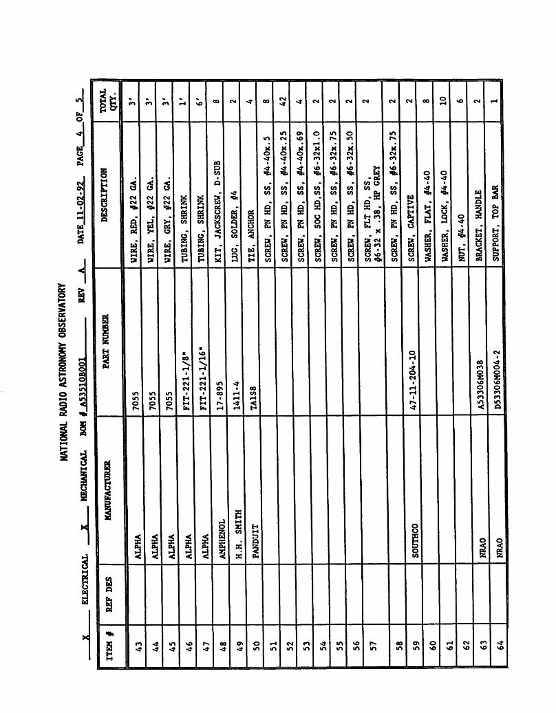
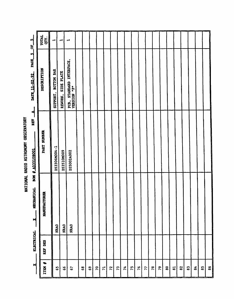
i 3 CO
CO O
s
X 00 VO
Ov VO
o 00
CM 00
en oo oo
•n oo
vo oo

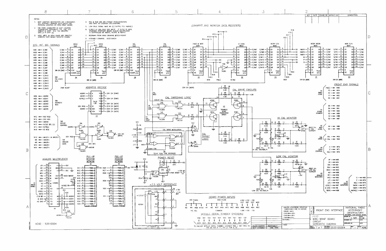


REV DATE DRAWN BY APPRVD BY DESCRIPTION
12-92 K. TATE D.WEBER REVISED AND REDRAWN ON ACAD
Al >* 1 T-
r SK R2 > D1 V
JSC* M
M 9 R8 8
R7 RIO R9 R4 R3 R6
■5g*« 9 R35 8
R34 R33 R32 R39 R38 R37
9 R51 8 R50 R49 R48 R47 R46 R45
16 R44 1
2E™ 5 R43 4
R42 R41
* AD584JH INSTALLED ON AUGAT 608-AG21 TRANSISTOR ADAPTOR
•• AUGAT 606-CG1 DIP HEADER *** AUGAT 608-CG1 DIP HEADER
ACAD : 53510A04
D5351QSQQ4 C5351QSQQ3 A5351QBQQ2 D5351QA001 NEXT ASSEMBLY
SCHEMATIC SCHEMATIC sm. ASSEMBLY
DWG. TYPE
FRONT END INTERFACE
] F117 k WIRE-WRAP
PRINTED CIRCUIT BOARD COMPONENT LAYOUT
SHEET «, * NUMBER 1 OF 1
NATIONAL RADIO ASTRONOMY
OBSERVATORY SOCORRO. NEW MEXICO 87801
DRAWN BY K. TATE
OESCNED BY
DATE 12-92 DME
AT LAYOUT APf,W(M3)BY ["
!gg A53510A004 V" A l3^ NONE

KVBiONS
aev out WWW IT APWD Br OeSCWFTTON
iwum IY
K. TATE OESGNGD IT
APPWYED BY
OHE
11-92 0*TE
DATE A53510A004
NEXT ASSY
ASSEMBLY USED ON
NATIONAL RADIO ASTRONOMY OBSERVATORY
SOCORRO, NEW UEXCQ17801
Y L B A
PROJECT FRONT END INTERFACE
mi F117 WIRE-WRAP PRINTED CICUIT BOARD BOM
owe NO. A53510B002 SHEET 1 Of
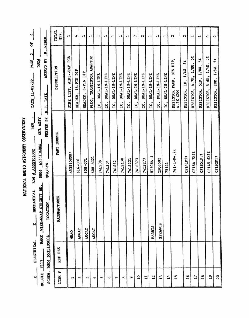
<t
a TOTA
L Q
TY
.
r-l -* r-l r-t t-l r-l r-t r-l r-l r>» CM r-C r-l ft CM CM r-l r-l <t CM
Cm O
CQ
CM G * * oQ ai »4 M
•e. Si O 0 - m M m M rn O BQ 1X4 H O4 « m m
^ Q e O4 IH m » «
§ 04
(14 1 CO aT 00 00 < OO
i S t H4
s 5 »-l 04 11 <» f* \ r-l \ 58
• Q M Oi Id (d (d Id Id Ul Cd (d td Cd O ^v r-i r4 m O O Z ja 25 25 SS 25 25 2; 25 25 t-l - • fid 2 H n n I-I »-i M tH M l-« 1-4 1-1 A u: ak Ui m
CM M h-l 2 CO -J ►4 -1 -J ►4 r4 ►4 _) ►4 J Ui •> r- NS vO Ui Ov & Pk I-I 1-1 • 1 • • I O u • r4 * 0 1 to
Id i CU CO 5Z 5a 55 2; 25 S5 Z 25 55 25 < ft ** m m CM
CM M vO § 52s M 1-1 t-l I-I l-l 1-1 1-1 •-1 1-4 i-« O4 o Q E-* r-l 00 <c • • • t ■ 1 - • • - . 1 CO OS _} Jl J) -1 ^ .-J J> ►4 »4 »4 04 £ 0$ ai OS OS OS
r-i td M - m {-t <: < «< <: «< < -< < < < O S 0 O O O O r-l H •J OS OH P P P P p P P P 3 P H O H H H H f-* s w m M 0 Q O Q 0 O CI Q 0 O CO CO CO CO CO CO w H W 0 >-< * •-4 M 1-4 I-I 1-4 H cn 3 «2 D . > . •. > • • • • « eo r>. CO CO CO CO CO < # !_» u w 3 0 O O O 0 O O CJ 0 O id • td td td td td Q fc
^ » X X o* M »-i 1-1 1-4 «-4 1-4 1-4 1-1 1-4 1-4 otf <a- OS OS OS OS OS
>- l >* & ec CO PQ
e I 3 a <
1 2 ^ 00 P4 CQ 3 o S
>- <» «
s CM o o CQ
o
1 r-l in
I I*- o o r-l m •4 fr« m »4
m in Ui »-<
O en as r-l r-l CM 00 r-l <n en • CM oi m r- Ui vo m
< r-« in , o o O O 00 <* CM en CM !••>. r-« < O • M • r-t • U. in < CO II r-l O O < O O en r-t CM en CM vO in r-l ft r-l •* m m CM
o en 2 11 m « 1 1 CO 2 CO 2 CO CO CO O \o <f • -* 00 CO <f CO m to || en VO 00 09 -1 ►4 —1 #-] ►4 m <y r-l r-l r-l r-l r-l r4 r-l < ■>>. v^ H m r-i 0 O <r -* <* «* -4- <f >J M ru in vo (K4 U* tt, Ui u*
§ *' 8 S -SO' || < VO vO VO r* r^ p» r^ r^ rs. p- X frt r» r>» O O U O 0
H —J « 2$ s ^5 I-H c K- J * S a **
5 o 1 • ». •<
M H 1 £
►
5 * m
5 i H H H
CO I-I
P 0
o g < 0
< 0 § 3
■ Ci3 ^1 || ttj P Q p <j 04
ac o || s <: «< < X CO
d 3 8 |l ||
S o
\
r-t m en m
CO w
r . Ii S 2
1 *»*
» < i 1 5 0 s H
r-( CS en -3 m vC r* 03 <^ 0 rH
rH r-i
en fi ft
in r-l
VO t-l t-H
OO r-l
ejv r-l
0 CM
O to M
a jZ 04
OQ O Q td • -H
td td CO OS OS £
OQ M <
VO CM
(fl M
Q 04 td oS a
td -H
td CO Oi I-I l-l 3 1-4 J*
vo CM
^ OS CQ M
H 04
3 O td -H
td CO OS 1-1
m m
04 H4 <:
Ov O m
en in
vo m
00 m
CM vo
en vo

8 5 4 DRAWN BY APPRVO BY
CPU ADDRESS/DATA BUS
CDNTRDL/MONITOR LINE BUFFERS
D
C
B
WARNING i CPU Ul VILL NOT BUN IF LINK 'R' IS LEFT FLOATING. IT MUST BE TERMINATED TO LINK
»5T I
I RESET 1 SWITCH
A
d— I
Z Z Z Z 2
12 BIT ANALOG CDNV. FROM U14 (SHT 2)
INSTALL HAND VIRE LINK TO P1.7 OR DESIRED SIGNAL
ACAD : SIBDSK-1
n^"17^ R/U
U13-1 CSHT 2)
DESCRIPTION REDRAWN WITH ACAD I
♦ 5V
MT ACTIVE
DATA OUT
PARITT
-H^—JBUSV -t*^^ 1 KSG ACTIVE
ACTIVITY INDICATORS (EXTERNAL)
NOTES i 1. ALL IC's ARE 'LS' LOGIC UNLESS QTHERVISE INDICATED. 2. USE EXACT PART NUMBERS ONLY ON Ul, U2, AND U5. DO
NOT SUBSTITUTE. 3. BYPASS CAPACITORS C01 *Cx* ON ASSEMBLY DWG.) NOT
SHOWN. 4. * = NOT USED. 5. ALL RESISTOR VALUES ARE IN OHMS.
CPU, MEMORY, AND I/O DRIVERS
NEXT ASSEMBLY
UNLESS DIMEN^
OTWERWISE SPECIFIED JONS ARE IN INCHES
! STANDARD 5 INTERFACE ? BOARD STANDARD INTERFACE BOARD MODEL *D* SCHEMATIC DIAGRAM
NATIONAL RADIO ASTRONOMY OBSERVATORY
SOCORRO. NEW MEXICO 87601
APPROVED BY
D
C
B
A


4 3 2 DRAWN BY APPRVD BY
REDRAWN VITH ACAD j
D
C
LI "^
B T
l R/w
U16-I2 - (SHT I)
»*5V D1STR
DEVICE ACKNOWLEDGE
IDR U2-39 -
(SHT 1>
ANALOG ENABLE
L> LSOO
U15 .
D
U16 6
91 Uls'V5—
CHI* CH1-
CH2+ CH2-
CH3t CH3-
CH4+ CH4-
CH5t CHS-
CH6* CH6-
CH7t CH7-
CH8* CH8-
S/H CONT
SiKY 5TR5
U16 LS04
i>^
iD/ TO Ul-12 • CPU INTR-0
(SHT 1)
/ H = DO-Dll IS IN HI-Z STATE L » DO-Dll DUMPED DN BUS
♦ 15V DISTR
ANALOG
EN1 EN2 EN3 Bl] EN
' CONVERSION IN PROGRESS) OUTPUT DO-Dll
SHORT CYCLE
-15V ANALOG COMM
DIG AO Al A2 A3 GND
DLY OUT
SDM854BG (BURR-BROVN) ANALOG DATA ACOU1SITIDN SYSTEM
CONFIGURED FOR
8-CHAN DIFFERETNTIAL INPUTS BIPOLAR OPERATION (tlOV RANGE) 12-BIT RESOLUTION (4.8828 nV/BIT) 2's COMPLIMENT OUTPUT CODING OUTPUT IS Of. 12-BIT VDRH Hl-Z DRIVEUS
DLY ADJ
ai [ii [ii
IY 2Y 3Y 4Y
SEL U6 5LL 74LS157 1A IB 2A 2B 3A 3B 4A
ADDR BUS DRIVER
RAO- RA1- RA2- RA3- RA4- RA5- RA6- RA7-
U4
A5 A6 A7 DIR
ADDR-0 ADDR-1
u—ADDR-2 li—ADDR-3 '-2— ADDR-4 lfi—ADDR-5 &— ADDR-6 iS—ADDR-7
ADDRESS BUS
U19 BURR-BROVN
INA101CM INSTR. AMPL.
-CDN/MON-4 -CON/MON-5 -CDN/MON-6 -CON/MON-? -C0N/M0N-8 -C0N/M0N-9 -CON/MON-10 -CON/MON-U -CON/MDN-12 -CDN/MON-13 -C0N/M0N-14
-C0N/M0N-15
CON/NDN BUS (12-BIT ANALOG CONVERSION)
TO PI (SHT 1)
IMSS nY/frU INSTALL JUMPER IN LIEU OF RIO
5.0 nV/bl-t INSTALL 240 OHM W RESISTOR PER BURR-BROVN SPECS
LOGIC COMM EXTERNAL ACCESSORY DC POWER AVAILABLE
FOR TEST AND ALIGNMENT
±15V CDMM
-15V
c
B
A
ACAD i SIBDSK-2
NEXT ASSEMBLY
ANALOG CIRCUITRY UNLESS OTHERWISE SPEOFIED
DIMENSIONS ARE IN INCHES i STANDARD °i INTERFACE 5 BOARD
STANDARD INTERFACE BOARD MODEL 'D* SCHEMATIC DIAGRAM
NATIONAL RADIO ASTRONOMY OBSERVATORY
SOCORRO, NEW MEXICO S7S01
A
APPROVED BY

4 3
NOTES:
A ONE WIRE ATTACHES TO Jll, PIN 20 ON REAR PANEL OF F117 INTERFACE MODULE, NRAO DRAWING #053510A001
2 REV DATE DRAWN BY APPRVO BY DESCRIPTION
D
C
& \
] C ] c : [
l c
it *J: 1 L
D
JII (REAR PANEL OF
F117 INTERFACE MODULE)
AS REQUIRED
c
B
A
VIEW A-A COMPONENT SIDE
ACAD : 53510A07 C53510S005 NEXT ASSEMBLY
SCHEMATIC DWG. TYPE
13 12 11 10
1
U5 U4 U3 U2 Ul R3, R4 P2 PI
B
ITEM NO. REF. DES. MANUFACTURER PART NUMBER UNLESS OTHERWISE SPECIFIED
DIMENSIONS ARE IN INCHES TUHtMMCB: MMUS *
I RACE OCCMMJ (JOOQ *
t HMX occnuLS (JOQ *
1 PLMX OCOUALS (.X} i
MATERIAL
FINISH
LM324 DG200 AD581LH MC7805CT 74S04 RC42GF102J DB-25S DB-25P
WIRE PIN, WIRE WRAP INTEGRATED CIRCUIT INTEGRATED CIRCUIT INTEGRATED CIRCUIT INTEGRATED CIRCUIT INTEGRATED CIRCUIT RESISTOR, IK, 2W, 5% CONNECTOR CONNECTOR GROMMET BOX, ENCLOSURE PERFBOARD
DESCRIPTION
J FRONT END INTERFACE
F117 LOOP BACK TEST FIXTURE ASSEMBLY
AR 18
QTY NATIONAL RADIO
ASTRONOMY OBSERVATORY
SOCORRO, NEW MEXICO 87801 A
K. TATE DESIGNED BY
L.D. MAY APPROVED BY
NUMBER 1 OF 1 NUMBER C53510A007
DATE
12-92 DATE
12-92
REV._ |SC^N0NE

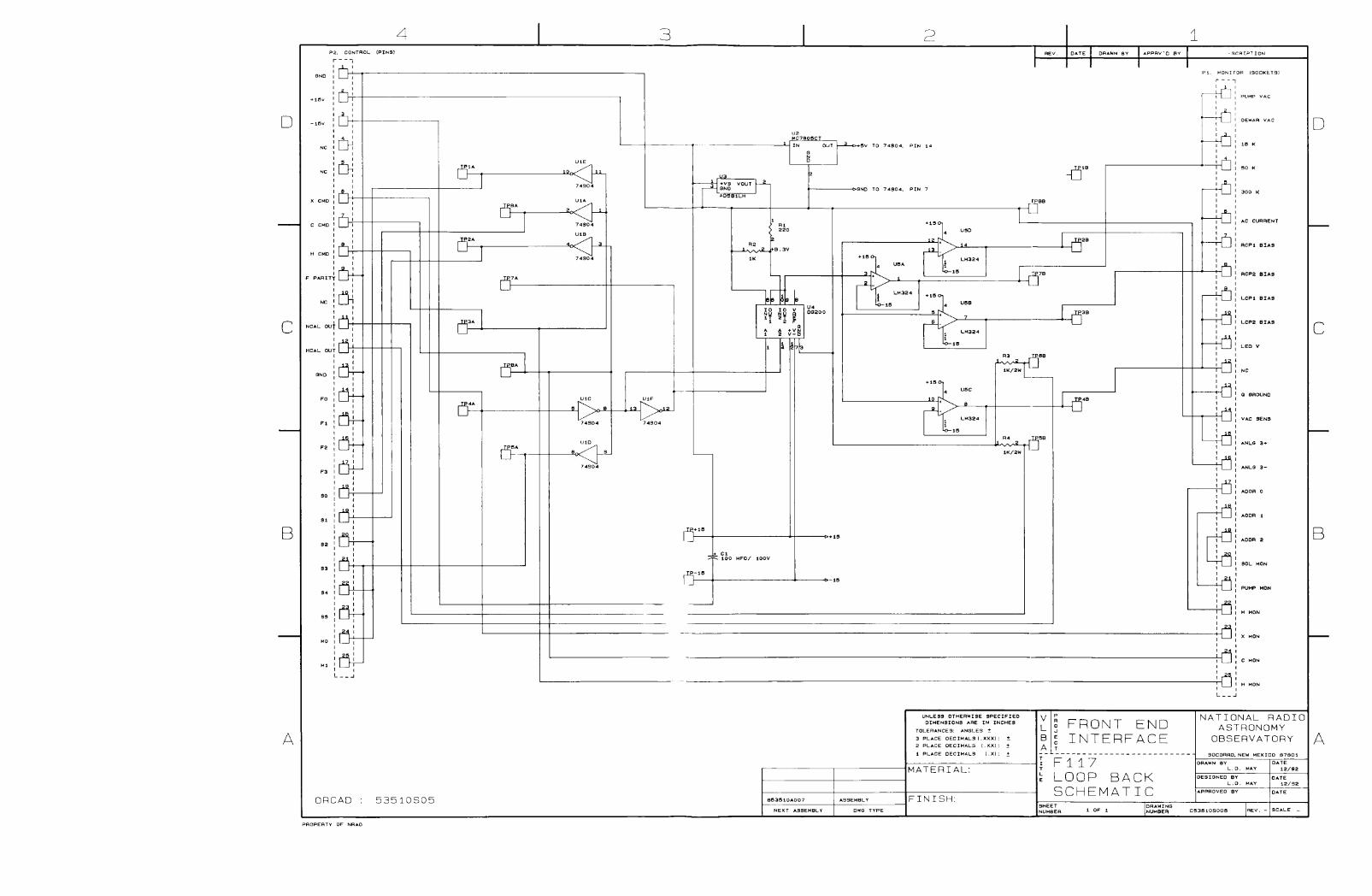
4 P2. CONTROL. (PINS)
D i
ItH
c HCAL OUT
B
d oi
d-
d d oi ioi d- OH
OH
A
ORCAD
PHOPERTY OF NR*0
53510S05
ff
JPZi
D-
ff
ff
ff
ff
ffA
7490 4
U1B
3 2
74904
IN OUT + 5V TO 7 490 4. PIN 14
—OQNO TO 74304. PIN 7
0 fc A +VN 1 s v-b
i J
IT!
iT=
100 MFD/ lOOV
-{J
UBA
-CT
R3 rPBB
J
--^\^2_-_r
DATE [ DRAWN BY
^
-O2'
■ff
■^
1
B53510A007
NEXT A99eMBLY
UNLE99 OTHERWISE SPECIFIED DIMEN9I0N9 ARE IN INCHES
TOLERANCES: ANGLES ±
3 PLACE DECIMALS t. XXX) : ± 2 PLACE DECIMALS (.XX): ±
1 PLACE DECIMALS (.X): +
MATERIAL
FINISH:
S FRONT END i INTERFACE
I Fl 17 Ls LOOP BACK
SCHEMATIC
-SCRIPT ION
PI. MONITOR (SOCKETS)
PUMP VAC
DEWAR VAC
0 MO
0 r40
0
o
0
o o o o
L^O 0
0^ ^O 0 0 0 0 0
AC CURRENT
fiCPl BIAS
RCP2 BIAS
LCP1 BIAS
LCP2 BIAS
Q GROUND
VAC SENS
PUMP MON
NATIONAL RADIO ASTRONOMY OBSERVATORY
SOCORRO, NEW MEXICO 87801
DRAWN BY
DESIGNED BY L.D. MAY
APPROVED BY
CS3010300B
DATE 12/92
D
C
B
A


4 3 2 1 CAL COMMAND
WRT. RD.
D
C
B
A
DIGITAL ID WORD RD.
2 C/MO 5 6
IS £ 15 16 C/M6
APPRV'O BY DESCRIPTION
UPDATED TO NRAO STANDARDS
DIGITAL ID WORD RD. so 3 OO OO
Dl 01 D2 02 03 03 D4 04 oa OS D6 06 07 07
OC G
2 SI 4 C/M5 S2 .!_.. 7 S3 8 34 13 C/M 12 35 14 13 C/M13
ASS 17 16 C/M14 H19 IS C^MIS R20
r-if" R23
CAL/HI-CAL DRIVER
4B-R4 V^—
20K
4B-RS SKS^S-
20K
"H _2.
NPN2E PNP2C
NPN2B PNP2B
NPN2C PNP2E
NPNiE PNP1C
NPN1B PNP2B
NPN1C PNP2E TF55352
QUAD TRANSISTOR ARRAY
-tic
REXT/CEXT
CLR T4L3221-
CAL CURRENT MONITOR
HI-CAL CURRENT MON
5C-R37 10K IX
•*atiu i* Lie R86 1 f
, 3G-R47 , 'W^ ■
3F-R41 - -^v
1 4p VCC
Ul Rl R2 R3 R4 RS R6 R7 RS
COM RIB R14 R13 R12 Rll RIO R9
12 P 113 A 14 R14 4 13 nis
... IS
16 6 11 21 17 ? 18 5 3 R1f)
76 L DCC16 C2 IS CONNECTED WITH THE POSITIV SIDE TO PIN 2 AND NEG. TO 9.
-tf 4B
R5 ' 06 R3
" . Rt
"dfc it ia
it 4} R36
R37 . R3B R39 R32 R33 fl34 R3S
it
3EZ R40 R41 R42 R43
it- MOUNT ADBB4 WITH PIN S. THE TAB, CONNECTED TO THE
Ig HEADER PIN 16.
ORCAD
PROPERTY OF NRAO
53510S03 NEXT ASSEMBLY
UNLESS OTHERWISE SPECIFIED DIMENSIONS ARE IN INCHES
TOLERANCES: ANGLES ± 3 PLACE DECIMALS (.XXX) : ± 2 PLACE DECIMALS (.XX): +
1 PLACE DECIMALS (.X): +
MATERIAL:
FINISH:
60B-AG21
HI-LO/SEL
3/N1 3>N2
3/NB 9/N6
JE
C>M1
C/M3
C/M 11 C/MIB
LFS RFg ISK
300K iD YE A!ll LEO_ ama_
100 ^100
FRONT END
INTERFACE
F117 MODULE SCHEMATIC DIAGRAM
NATIONAL RADIO ASTRONOMY OBSERVATORY
SOCORRO, NEW MEXICO 87801
DESIGNED BY
APPROVED BY
SHEET NUMBER C53510S003
D
C
B
A


This wire list was abstracted from "Technical Manual, F117, FRONT END CONTROL MODULE " by E. Schlecht, July 1990.
VLBA FRONT END MODULE F117 INTERNAL WIRING HARNESS JULY,7,1987 DRAWING:A53510U006 WILLIAM WIREMAN NOTE: (L) INDICATES THE SIGNAL IS LOW TRUE, EX. HI-LO(L) LOLOW SIGNAL
PART I-WIREWRAP CONNECTOR WIRING
PIN FUNCTION SOURCE COLOR GA. PIN FUNCTION SOURCE COLOR GA. 1. GND REF GND BLK 22 2. 5V TB1-4 ORG 22 3. GND 4. 5V 5. ANLG 4+ PI-5 WHT/GRY 26 6. ANLG 5+ PI-6 WHT/VIO 26 7. 8. Q GND J1-13 BLK 22 9. *Q GND PI-19 BLK 26 10. ANLG 1 & 2+ PI-2 WHT/GRN 26 11. R/U(L) PI-49 WHT/BLU 26 12. DEV REQ PI-35 WHT/BRN 26 13. ANLG 6+ PI-7 WHT/YEL 26 14. ANLG 7+ PI-8 WHT/BLK 26 15. DEV ACK PI-36 WHT/GRY 26 16. ID READ P2-9 WHT/ORG 26 17. HI-LO(L)SEL PI-17 WHT/GRN 26 18. ANENB PI-37 WHT/VIO 26 19. S/N 0 GND/5V BUSS 26 20. S/N 1 GND/5V BUSS 26 21. S/N 2 GND/5V BUSS 26 22. S/N 3 GND/5V BUSS 26 23. S/N 4 GND/5V BUSS 26 24. S/N 5 GND/5V BUSS 26 25. S/N 6 GND/5V BUSS 26 26. S/N 7 GND/5V BUSS 26
NOTE: STRAP SERIAL/NUMBER TO PIN 27 FOR ZERO AND PIN 28 FOR A ONE. EX. S/N=18 STRAP S/N 0,2,3,5,647 TO GND PIN 27, AND S/N 1&4 TO +5V PIN 28
29. 31. 33. 35. 37. 39. 41. 43. 45. 47. 49. 51. 53. 55. 57. 59. 61. 63. 65. 67. 69. 71. 73. 75. 77. 79. 81. 83. 85. 87. 89. 91. 93. 95. 97. 99.
PI PI-
ADDR 0 ADDR 2 ADDR 4 C/M 0 C/M 2 C/M 4 C/M 6 C/M 8 C/M 10 C/M 12 GND C/M 14
CAL LF1 LF2 15 K 300 K VP LED(L) PA C GND H-MON(L) X-MON P
0 2 0 0 2 4
F F M S S S MOD 15V GND GND
48,J1-17 46fJ1-19
PI-44 PI-33 PI-32 P1-31 PI-30 P1-29 PI-28 PI-27
J2-11 J1-9 J1-10 J1-3 J1-5 J1-1 J1-11 J2-9 J2-7
J1-25 J1-23 J1-21 J2-14 J2-16 J2-24 J2-18 J2-20 J2-22 FT-6 TBI-6
WHT/VIO WHT/BLK WHT/BLK WHT/ORG WHT/BLU WHT/RED WHT/BLK WHT/YEL WHT/VIO WHT/GRY
BLU WHT/RED WHT/BLU WHT/GRN WHT/GRY WHT/BLU WHT/ORG WHT/RED WHT/YEL
WHT/GRY WHT/GRN WHT/BLU WHT/BLK WHT/BLU WHT/RED WHT/GRN WHT/GRY WHT/YEL WHT/RED RED
26 26 26 26 26 26 26 26 26 26
PI-26 WHT/BRN 26
REF GND BLK
22 26 26 26 26 26 26 26 26
26 26 26 26 26 26 26 26 26 26 22
22
30. 32. 34. 36. 38. 40. 42. 44. 46. 48. 50. 52. 54. 56. 58. 60. 62. 64. 66. 68. 70. 72. 74. 76. 78. 80. 82. 84. 86. 88. 90. 92. 94. 96. 98. 100.
ADDR 1 ADDR 3 ADDR 5 C/M 1 C/M 3 C/M 5 C/M 7 C/M 9 C/M 11 C/M 13
C/M 15
HI-CAL RFI RF2 50 K VD ACI SENS H(L) X
C-MON M(L) S
1 3 1 1 3 5
-15V 28V 5V 5V
P1- 47fJl-18 PI-45 PI-43 P1-16 P1-15 P1-14 P1-13 P1-12 P1-11 P1-10
J1-4 J1-2 J1-6
J1-24 J1-22 J1-20 J2-15 J2-17 J2-25 J2-19 J2-21 J2-23 TB1-5 TB1-7
WHT/YEL WHT/RED WHT/YEL WHT/ORG WHT/BLU WHT/RED WHT/BLK WHT/YEL WHT/VIO WHT/GRY
J2-12 VIO J1-7 WHT/YEL J1-8 WHT/BLK
WHT/BRN WHT/ORG WHT/VIO
J1-14 WHT/GRN J2-8 WHT/BLK J2-6 WHT/VIO
WHT/BRN WHT/ORG WHT/RED WHT/RED WHT/ORG WHT/BLU WHT/BRN WHT/VIO WHT/BLK YEL GRY
26 26 26 26 26 26 26 26 26 26
P1-9 WHT/BRN 26
TBI-4 ORG
22 26 26 26 26 26 26 26 26
26 26 26 26 26 26 26 26 26 22 22
22
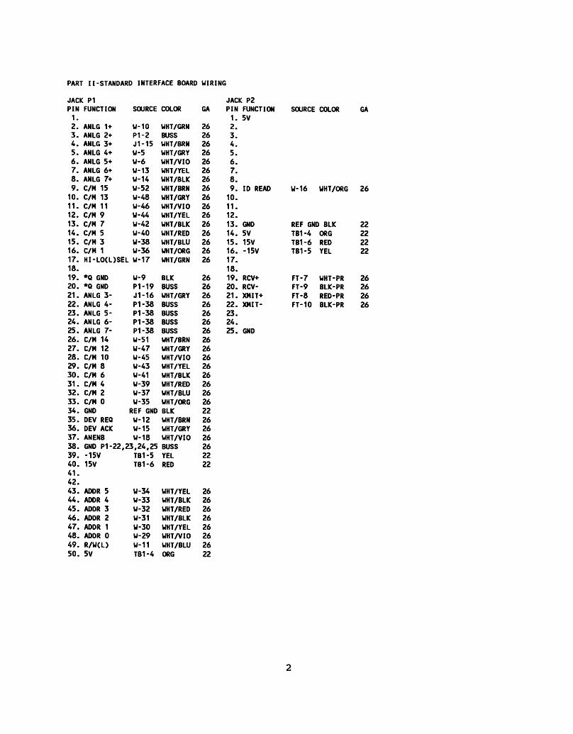
PART 11-STANDARD INTERFACE BOARD WIRING
JACK PI JACK P2 PIN FUNCTION SOURCE COLOR GA PIN FUNCTION SOURCE COLOR GA 1. 1. 5V 2. ANLG 1+ W-10 WHT/GRN 26 2. 3. ANLG 2* P1-2 BUSS 26 3. 4. ANLG 3+ J1-15 WHT/BRN 26 4. 5. ANLG 4+ W-5 WHT/GRY 26 5. 6. ANLG 5+ W-6 WHT/VIO 26 6. 7. ANLG 6+ W-13 WHT/YEL 26 7. 8. ANLG 7* W-14 WHT/BLK 26 8. 9. C/M 15 W-52 WHT/BRN 26 9. ID READ W-16 WHT/ORG 26 10. C/M 13 W-48 WHT/GRY 26 10. 11. C/M 11 W-46 WHT/VIO 26 11. 12. C/M 9 W-44 WHT/YEL 26 12. 13. C/M 7 W-42 WHT/BLK 26 13. GND REF GND BLK 22 14. C/M 5 W-40 WHT/RED 26 14. 5V TBI-4 ORG 22 15. C/M 3 W-38 WHT/BLU 26 15. 15V TBI-6 RED 22 16. C/M 1 W-36 WHT/ORG 26 16. -15V TBI-5 YEL 22 17. HI-LO(L)SEL W-17 WHT/GRN 26 17. 18. 18. 19. *Q GND W-9 BLK 26 19. RCV+ FT-7 WHT-PR 26 20. *Q GND P1-19 BUSS 26 20. RCV- FT-9 BLK-PR 26 21. ANLG 3- J1-16 WHT/GRY 26 21. XMIT+ FT-8 RED-PR 26 22. ANLG 4- P1-38 BUSS 26 22. XMIT- FT-10 BLK-PR 26 23. ANLG 5- PI-38 BUSS 26 23. 24. ANLG 6- PI-38 BUSS 26 24. 25. ANLG 7- PI-38 BUSS 26 25. GND 26. C/M 14 W-51 WHT/BRN 26 27. C/M 12 W-47 WHT/GRY 26 28. C/M 10 W-45 WHT/VIO 26 29. C/M 8 W-43 WHT/YEL 26 30. C/M 6 W-41 WHT/BLK 26 31. C/M 4 W-39 WHT/RED 26 32. C/M 2 W-37 WHT/BLU 26 33. C/M 0 W-35 WHT/ORG 26 34. GND REF GND BLK 22 35. DEV REQ W-12 WHT/BRN 26 36. DEV ACK W-15 WHT/GRY 26 37. ANENB W-18 WHT/VIO 26 38. GND PI-22, ,23,24,25 BUSS 26 39. -15V TB1-5 YEL 22 40. 15V TBI-6 RED 22 41. 42. 43. ADDR 5 W-34 WHT/YEL 26 44. ADDR 4 W-33 WHT/BLK 26 45. ADDR 3 W-32 WHT/RED 26 46. ADDR 2 W-31 WHT/BLK 26 47. ADDR 1 W-30 WHT/YEL 26 48. ADDR 0 W-29 WHT/VIO 26 49. R/W(L) W-11 WHT/BLU 26

PART III-REAR PANEL CONNECTOR WIRING
JACK 11 (AMP 42 PIN) PIN FUNCTION SOURCE COLOR GA PIN FUNCTION SOURCE COLOR GA 1. 2. 3. 4. 5. 6. 7. 8. XMIT+ FT-8 RED-PR 26 9. XMIT- FT-10 BLK- PR 26 10. 5V FT-2 ORG 20 11. 12. MOD FT-6 WHT/RED 26 13. 14. RCV+ FT-7 WHT-PR 26 15. RCV- FT-9 BLK- PR 26 16. 15V FT-5 RED 20 17. -15V FT-3 YEL 20 18. 19. 20. 21. 22. 23. 24. 25. 26. 27. 28. 29. 28V FT-4 GRY 20 30. 31. 32. 33. 34. GND FT-1 BLK 20 35. 36. 37. 38. 39. 40.
PART VI-FRONT PANEL CONNECTOR WIRING
J1-I MONITOR J2-I CONTROL PIN FUNCTION SOURCE COLOR GA PIN FUNCTION SOURCE COLOR GA 1. VP W-65 WHT/BLU 26 1. GND REF GND BLK 22 2. VD W-64 WHT/ORG 26 2. 15V TBI-6 RED 22 3. 15 K W-61 WHT/GRN 26 3. -15V TBI-5 YEL 22 4. 50 K W-62 WHT/BRN 26 4. 5. 300 K W-63 WHT/GRY 26 5. 6. ACI W-66 WHT/VIO 26 6. X W-72 WHT/VIO 26 7. RFI W-58 WHT/YEL 26 7. C W-71 WHT/YEL 26 8. RF2 W-60 WHT/BLK 26 8. H(L) W-70 WHT/BLK 26 9. LF1 W-57 WHT/RED 26 9. PA(L) W-69 WHT/RED 26 10. LF2 W-59 WHT/BLU 26 10. 11. LED W-67 WHT/ORG 26 11. CAL W-55 BLU 22 12. 12. HI-CAL W-56 VIO 22 13. Q GND W-8 BLK 22 13. GND REF GND BLK 22 14. SENS W-68 WHT/GRN 26 14. F 0 W-81 WHT/BLK 26 15. ANLG 3+ PI-3 WHT/BRN 26 15. F 1 W-82 WHT/RED 26 16. ANLG 3- PI-20 WHT/GRY 26 16. F 2 W-83 WHT/BLU 26 17. ADDR 0 W-29 WHT/VIO 26 17. F 3 W-84 WHT/ORG 26 18. ADDR 1 W-30 WHT/YEL 26 18. S 0 W-87 WHT/GRN 26 19. ADDR 2 W-31 WHT/BLK 26 19. S 1 W-88 WHT/BRN 26 20. S W-80 WHT/RED 26 20. S 2 W-89 WHT/GRY 26 21. P W-79 WHT/BLU 26 21. S 3 W-90 WHT/VIO 26 22. M(L) W-78 WHT/ORG 26 22. S 4 W-91 WHT/YEL 26 23. X MON W-77 WHT/GRN 26 23. S 5 W-92 WHT/BLK 26 24. C MON W-76 WHT/BRN 26 24. M 0 W-85 WHT/RED 26
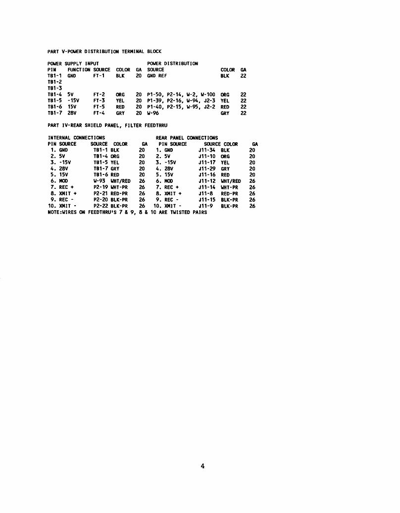
PART V-POWER DISTRIBUTION TERMINAL BLOCK
POWER PIN TB1-1 TBI-2 TB1-3 TBI-4 TBI-5 TBI-6 TB1-7
SUPPLY INPUT POWER DISTRIBUTION FUNCTION SOURCE COLOR GA SOURCE GND FT-1 BLK 20 GND REF
5V FT-2 ORG 20 Pl-50, P2-14, W-2, W-100 -15V FT-3 YEL 20 P1-39, P2-16, W-94, J2-3 15V FT-5 RED 20 PI-40, P2-15, W-95, J2-2 28V FT-4 GRY 20 W-96
COLOR GA BLK 22
ORG 22 YEL 22 RED 22
PART IV-REAR SHIELD PANEL, FILTER FEEDTHRU
INTERNAL CONNECTIONS REAR PANEL CONNECTIONS PIN SOURCE 1. 2. 3. 4. 5. 6. 7. 8. 9. 10.
GND 5V -15V 28V 15V MOD REC + XMIT + REC - XMIT -
NOTE:WIRES ON
SOURCE COLOR TB1-1 BLK TBI-4 ORG TBI-5 YEL TBI-7 GRY TBI-6 RED W-93 WHT/RED P2-19 WHT-PR P2-21 RED-PR P2-20 BLK-PR P2-22 BLK-PR
FEEDTHRU1S 7 & 9,
GA 20 20 20 20 20 26 26 26 26 26
PIN SOURCE 1. GND 2. 5V 3. -15V 4. 28V 5. 15V 6. MOD 7. REC + 8. XMIT + 9. REC - 10. XMIT -
8 & 10 ARE TWISTED PA
SOURCE COLOR 11-34 BLK 11-10 11-17 11-29 11-16 11-12 11-14 11-8 11-15 11-9 RS
ORG YEL GRY RED WHT/RED WHT-PR RED-PR BLK-PR BLK-PR
GA 20 20 20 20 20 26 26 26 26 26

5.0 DATA SHEETS
This section contains the following data sheets:
Front-End Data Sheets
Front-End Vacuum Pressure as a function of Monitor Output Voltage Front-End Card Cage Assembly, D53203A004
F117 Data Sheets
HI506A Harris Analog Multiplexer LF442A National Semiconductor Operational Amplifier LM393 National Semiconductor Analog Comparator AD584 Analog Devices Pin-Programmable Voltage Reference TPQ6502 Sprague Quad Transistor Array 75141 Texas Instruments Dual, Single-Ended Line Receiver
F117 Loop Back Test Fixture Data Sheets
AD581 Analog Devices High Precision 10 V IC Reference LM324 National Semiconductor Low Power Quad Operational Amplifier HI200 Harris Dual SPST CMOS Analog Switch
63

64

^\
-
10000 ot-^ Atmosphere
s* j
A / 9652 ot
1000/im"
- /
^ -
1000
500 h
300
200
100 70 50
30
20
10 7 5
3
2
1 2000 4000 6000 8000
Monitor Output (mV) Vacuum Pressure as a Function of Monitor Output Voltage
Jll JO J9
3IJEQ@H


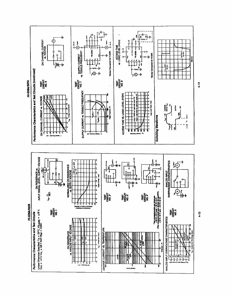
i i o 2 a:
6 ■Jb
i< u z o
o
1: ^Htrl"
7 s ^
-if
1 / 1
k f= p — — i o
c **•
- > / > __ -*
yw *IMU<I3 A|M^ - l«|M.im»v
s s
'i-l TT; 1
Si
to »-
5 +
•X
■s2
lUQ it tea.
«8
1
< «? "f^
_ 7 T
: ? f
= 2 = = = = 33
_
.
1 S 1
~
I

f * 1
i—fl*1 Trl
i^aki I
^9 1Q
sS^ ^g
i
<J ̂ . >— J r s
.a i '■"
•A
^
«» _o.
^ =i
u
Uj rfl'
85
-VSAJ^
ItttC Mi-
l€Hi'
2 UJ. / 9 uA 5 g
s M
^ rr -3A o
1 ^ Uj 9
— 1 Eo
L"
iii w 5> I-fr
LiA v^-i-
si
cl
'cxlr x j r
a S • «. 1
i =iR
^d?:
3^1 Sir
&j-lh
^ ^F-'
-S^d?:
0 5f.

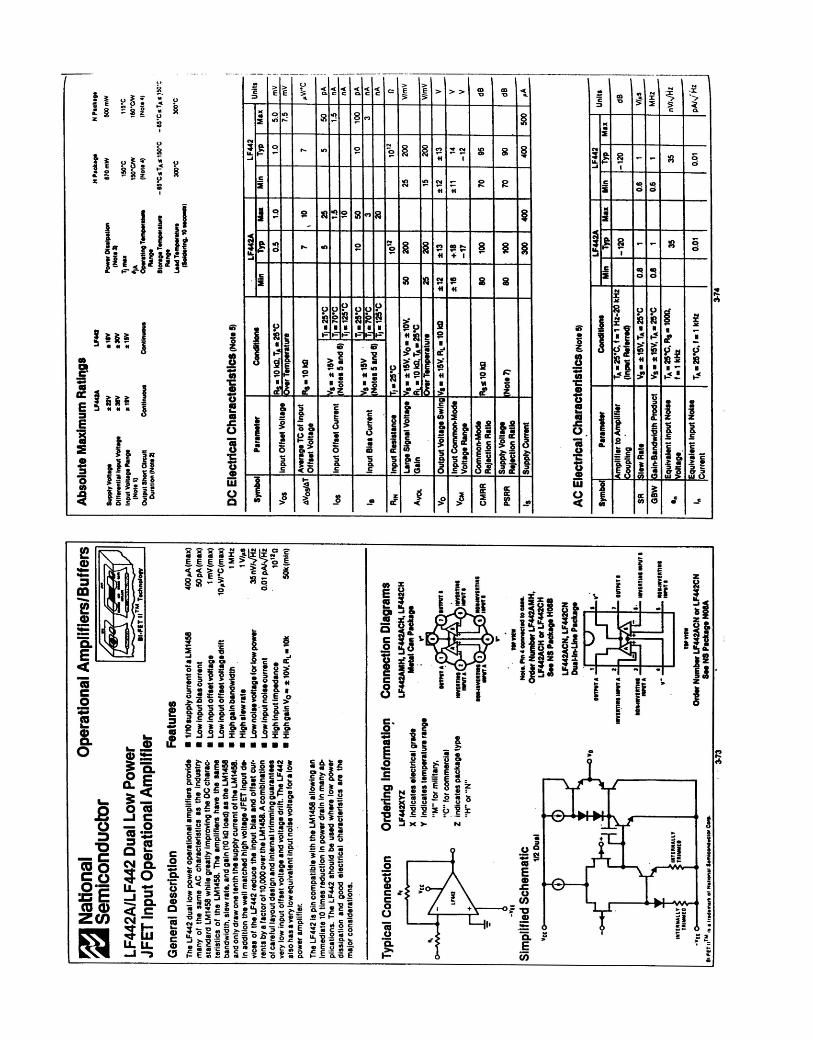
!i
8 V § ^ <
s
2 a 5 *
?*£
iiij»in«
I igi M 2
C 3 « « « S
J 2 j o 3
O CO
2 !iMl 3 S £ 6
8 •c ©
s IS
o 8 •c o « tu O a
< o
>1
^^
< a E E > > >
^2
I'o
I ii
fi IS
a. .2.
1 - 1 c 3
■a •o ^ r 5
c Q.
■
CM
s
3 u. -I s
1 - '- S O
o
c <o (O S o o
IL
S
* 8 - ^ 8 o o
_J i
£ m « 2 o o
N z 8 U o
§ » j -s 8 R i
• 1 D* .* V
^ V if 1
*» o z* » ^5 o o Sij 41 « »* 8
M & 1 K
(0 ^s d? d? ►5i ^ •c a> Z 2
i s | I
s I I
: 1 I
^IM m O J CO £
If i • CD ? ft ■3 §
13 t3 4$ 1 t m H IU ^ o
M OC in
t< > o ^ > fs ^ 8
-_ SS 1 c
ff « « s
s Q. O
o 3 "O
■= c CD O
13 E (0 0) ZU)
!i O CO J c
=! Q. < JE CM r-
U. UL
til Siiifafll e _ S 1 ll
!!
5 &
"5 & to ©
© c ©
£££ ISS l?€ 118 s *» •
I » « •> c
P! O -c Q. = • E ?s>. fl! -^ i s s * = ia <s « •«
-"1 en — -I ? o2 u. « -J >.'0 •SS H- E •)
Hi!* - Jti lSo% s s • s • o t 2
' = S Ss tit S • "-p CO**
■n -C •= >_j g — O Si • £ a
j S • •
OS* § •» 2 >• =
S -a o TJ ~ c TJ 10 o <o c _
o E ap g.
21111 --2 £ =
2 « cp|
r - 3 ! ; E
* g .c 5
-J fe-g 5 5 1*2 £ &3 o
* CT.S •235 fi og • S o 9 •
si5' 8 CU. Olfi s •£ -o a
•> •> m ' S t2*
•. " c as" sl « ° i- 2 ~2 » o c 5 ■ c - o
• E o 2 «■ I- £ Q.-O E
If 'I St 5JJ 1 Higltfj) l
S 34 s 3 5 s L_
! ii!
• s s s
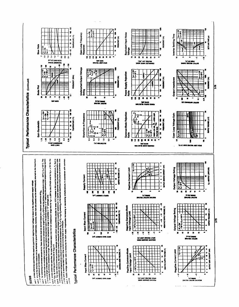
_-.-i::: - A
a 2
— • ■—M i__a 1 1 A
9 •
I* O a
-l«b 7 -•JJ V
/ / n
(t*/*) UVM mm MASCIKUEH)
S * 5
M
u S a
JO O 8
£ 8 Q.
X 8 S - S S i i
(wl mn
(IMNl HlOMMim NflflAUNn
SSS88S3B0
iMnoAMnnuo
8 8 2°
(?H/VA«I jmrwA ismuumuamma
h = = z
Wi- 3 ^ £ rJ
^ f\ ^ ̂ / ' / y
!l. J |— ?77 / »• 'rf /
/ j /
s 8
*i 8 |
B ■ B
" * *? " »= 5 8 '
I 3 a. I
Si —7
^ — * * y
^ = =:=
—
8
Si : r ' 7 7 » 1 1
^ / /
/
/ r /
■ — / /
9 8 g S g 8 8
IVIOUM NOUarMAUMSOMM
3=: = = =B„: VA ♦■fc-
8.
s § s to)
2 s
- s
is
*
tl 1 y f
/ r
-T—
1 1 As
/ UAV,
83888838-
(IflOUMI NOUarai 3Q0H-MMN03 (A/AI ma awnoA «oi ON
ii IS • c 2 8
ll I
iiiii
1=21£slfgfS
©
o S a o © o c ©
i o t: 8.
P a E
s 1 •M ■ ^ s ,s / .£ ^«- u
V i
- *
• 8 "I
1 5 8 » trOuaMmAUMs (AlMMU
mflOAUUlMlAUSU
1^]'::::::: |._":
I :::::: :s::: S it ,.. ? ^ 5.
8 8 eg
\ z
if IS II
Sk A, h AL s s_ ■ * SL » S s
MluoMinniiuuM
esse
fAlUMIJMnOAUWM ]0«MwnN3]«in»i
- s ' s X " ^ i ^ \ \ I sT- V \ Vi X
i I >> 53
8 8 2 •
Mi iNitnin svit ifWMt
T|
8
a
.1 s p
e
^ ̂
-1 == = =a ;— ^n 3
ev \ «s \ ll£S
8 8 8 s a (MAIMNS
mrMAiMina
1 s, v,
& - » -Si* •s
V, \, ^ V
I s
8 S
t*-*awmm mnoAuuino
s \ YA ■g *
<? y/ 3 jr '/? | ^si
/ s V « /
. 3
]9«no« uwino MIIVSJH
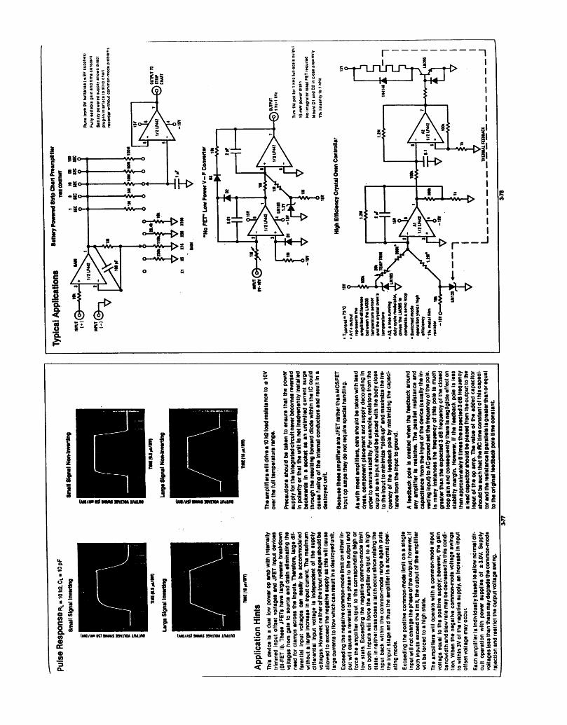
i^^-pOJilrLn-jV/—
WiM ii|iii»
•o c a • J, J. • ~ •= 2 ™ 2 • oi~ 5 — 5
• S « O S •
itllll
ar •- cl a.
£ o • o Q-o 5 ^ osr- ?»•
c c £ ■= o a • « O 3 S.I|E
Hfii Iflli
f-lss
i§ifi
** -S — O" •* Q. U
itji'iii' a?
r? Pis«»a S-EPS'-
m aZ c • 5 2 S £
!t «•g
ll ll
ll So
E Q.2 2 3
— — S • — ^ E 62
"2 * =; ♦^ so
i;f:IsPlii
i? of s •■=- Isf •
lilt
E»£5S oifc-5 •^53 " I & o « 5 g •MS
a o • c s: 3 —
O ■> <• C = 3 " ^ fc *- ^ B O 3
£ "o o I ^
• ffi
S-S--^0— a«I2S
< fsm §| . ,= o= S
c «>• • = o • £ <o |£o?
. « O.C
O • 3 m k
18 H o •
II 85
c Z. o com o • £ E • • c • — 2 o o. E 2
, o 'o s £ > > ♦- rz r^
c io ~ S • • Q « £Sei2 o « -: c o • •
■p = £ • s * • • o _ o J
*s 2 • 3 £ = ^^ c»
g£ an a o
« ci - o> • " x Z S • o.c 2 g
a S x c -o £ « 2.= =
i JC •) o _ S 3 c •o a. E — c
5?c
lis o f o ■ s- • •C 3 • i "* SIE a a- «
III torn
|S5 a • 5
" <0 TJ • = C c o a I- > £>
ll H It o > • • 3
■1 >> •
"SB • 3 E EOT S
Ml? i«8S o o £ o>
mi = • o i
• go
cos.
52 =
£§?5 5 * • 2 fec£ S 2 o « TJ = s » c o. « • • E • *> £ 5 o. « o • o as c • o o S •; • .2 3 o "S"
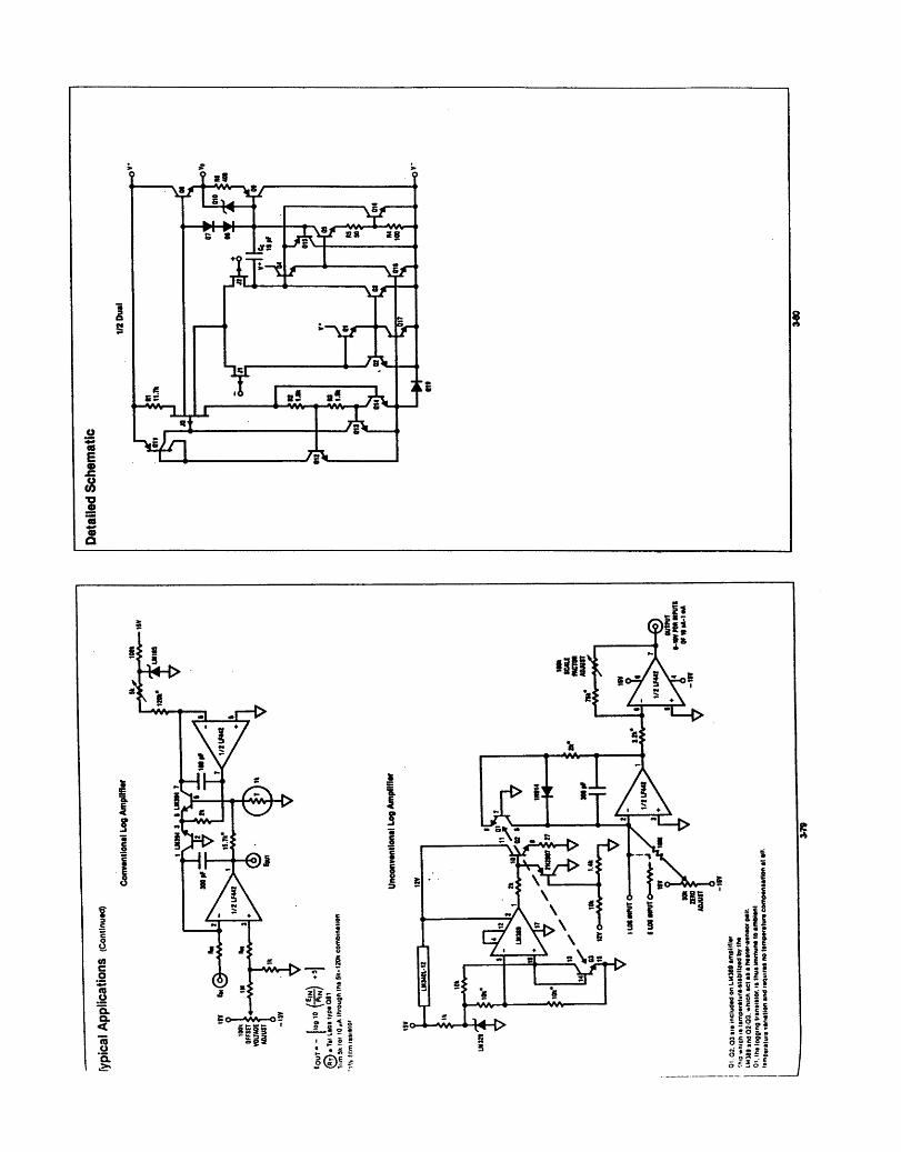
m E ©
"8
53
■W-M- & 8
|«yg ,J,5V-J—
SS 28
■vy
T /iV.
L%i(£Fj[
ss a~ i ^^i fin i ^^II f f s
/Pi.
©
ex Q. <
a
i—"VAAf—^>
.O 5
•HIX
t I *++* »
Lt 12 K 8=?=
*'> \ I i
8 > Wf *
\ Ass
8 -vvv-
8| s s.-f | E * « i 2 Is**! SI:ii 3 S « - | -* • o S £ § f e i i 7 3 u S ■ I S ? » £ 1 8 » c 2 y c « 2 « -E • O Z. £ • 2~ ?s • - O a • ■i c g tf 5 q|gf|
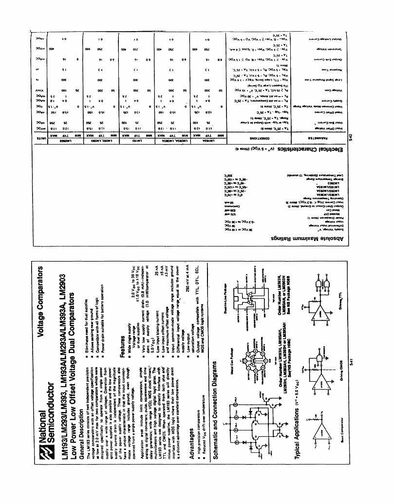
3.SZ - vl oov„ 1 0 10 1 0 1 0 10 DOA S . OA OOA I < 'NIA 0 - "N'A
3„SZ - Vl
lu>iin3 •6<M>1 indino
DOAU. 00» OO* ose oo» Oil 00> osz OO* OSZ vui » > XNISi 0 - ♦NlA MA 1 < NIA
3„SZ ■ vl
«6«i|OA uo*l*(ni«^
30v.u 91 9 91 09 91 09 91 09 91 09 'OOA SI > OA o - ""A MA I < "'A
Ii ••ONI
lu»..<i3 nu.s indino
irt SI
ooc
C'l
ooc
t I
OOC
CI
OOC
CI
OOC
o. sz ' wi Hi i s - 1M MA S - TIA
D.SZ ' vl Ml IS ' 1M MA S ■ ''"A MA » I - J3MA •""•S J-eoi m . NIA
(6u.««s OA ••<«1 uoddns on
A<"/A 001 K OOl OS ooz OS OOZ OS ooz OS MA SI » ,A 'D0sz - *i ui si < in u.»9 ••tilOA
OOyu, sz 1 <il sz sz 1 SZ I 3OA0C - tA'«l™VIIVuo—■ "»«
DflVU. 0 1 »0 1 »0 1 »0 i to I ► 0 3.SZ • *! •noitj«duMO nv ua _ . l)j liMun^ Aiddos
30A Sl-,A 0 Sl-4A 0 Sl ,A 0 Sl ,A 0 Sl ,A 0 19 MONI D.SZ ' Vl aautu (fellOA apoM UOUMUOO indui
DOyu 091 os» OST OSJ SZ' OC* OS* os> SZl ox» 3.SZ • Vi • Nl|- «NI|
IS mNl O.SZ - Vl ••utu
lu*ijn3 IOHO indu)
OOyu OX K 09Z sz 001 sz osz sz 001 sz JUIM-I u| mdrno mm -Nil to *H\\ x luuma mg indu|
30A«, OH OH OS! ou OS. Oli 01. Oli OZi Ol» l«»»oNI-3.SZ-Vl ••(UOA muO I"*"!
UINO XWN 4AL nm XVM MI nm XVM 4Ki. NNfl xvn 4A1 NIM XVM 4K1. NM*
SNOIIKMKX) H313WVIIV4
(» WON) JOQA 9 - +A) so!)S(japejeqo (eopioaig
D.O0C (tpuoMi 01 tuiMpiosi •initMduwx pw-| 3.0Sl»«»D.99- atutH *jniiNdiu«j. •teaois 3.S8»<»D.0»- C06ZM1 3.SZl»m3.SS- vceim/ceim 3.S8»«>D.SZ- VCUM1/C6ZW1
3.IW* •» 3.0 vcacMi/cacMi «ttu«|| •initiaduMX fuiisjado
V«»0S (t •ION) IMA CO- > "'Al lu»iino indui tnonwiuos IZ MOfi) 'punoig oi inaji3ijoi|s indino
AAV DCS <«3l«i»M
AAWOU dlOP»Pton (| JlONl IMMMdnuQ MMO^
MA gc»<>iMA CO- •ttiioA WKhii
MA 9C a6*i|OA I"*"! IWIMUIIIO
DOA8IJK>DOA9C ^A '••«|OA Aiddns
2 o a (0 Q. E o o a> O) CO «••
£ o •o
75 o 5 9 X3 E CD 0)
CO o
CO »- o) a CO o. S E -1 o
-J <D
CO 2 ?5
^ ^ 0)
CO" » co O
ll == o CO Q.
S o
o o •>
• o <£> OS -O S rj — c •
2o IS o- < E o o - '
< < > c c E Ii
S E
= o
tt »- 2 S-o 2 S «» c 2 a
- 5 a 5 ill! iu < o S.
z * if i s
..i - -5 > >
Miff 3 3 g ^
© % > TJ IO -J
11! £ | o
£ E O 3
!!
£ -s
^,
If
I* lis lis £ 5 3
S? -f
€
5 5. 6 -
& 0- I&8 3 » OO
0 ? 3? .5
ill
c c » 0 o s
Hi • •* f c Si o as S I1! 1 5 *>
lilini • o $ f s g
5&££|lSc.
oj>"«.a — 3> •t ?• £ S s o >
-oSll|!^£Si ls!l°o|f.Hll t!-c2«?"3'-o-2c5 a 'c w •*'••• •" a Q
S 0 S .9- If
Q s s ~ Q.O TO S |^
© • 5 a £ s
2 £
fs-itii ft O <• 3 H -
v >- t S <* 2
^1£ ~ - = = a r 2 "8 & M 3 o £ E o
<0
E S2.
c o u © c c o o TJ C © o w E « u
CO

O) s _
- H — : ■ -* ^j:—
("•AI imnoA MMimMin- "A
8 I
8 c u1 , U ii -] P" -
- li ■ 1- T
8 s 2
M •c ©
IS s ©
o © o c ©
i o
1 © o o. .>«
I!
!* 1
ill 111
*-; = 4Vfr- ,1
133323-18- (Al ** (A*1! MA
19V110A 1*41*9 iVtfWAUUm
g 1 M 1 * A"
!&:::::
- a
sass trl uimiM AIMM - ^
" = 35 ("Al 19V110A uuwiaivt^A
1 i il ill III
■i-m
.1
8 A
.1
nrmaiwHU tvuM
'(^OA 9"I- +A « 30A o) •*'•' «po»u-uo»muoj indui H"! Mil 0*0 put :DOA OC <» 3aA S ""'I +A Ml!*" U0 • SU ':>0A ► I « OA 'iwod tpiHW mdine»V =• matt (pmn |!'A|<Mm MMOd•MIISOU MH |0opniiuaouiost MOfqOOACOM) 30A CO-UOH*"(I•Q wu Wtui•»•>« ofcllUAindu)
MO| am-«nt indino Mdojd t apiAOjd HIM jownduios pip *«>u«i opoumouiuioa mt uwpwA «m»iu»i «6»>|OA i»mo in w «uo| «y -|*M|A|diim MMOd wo potaxm A«iuia*i|OA indu) to tMO)ijn»i»» xnmo^ :a<*oM uoiiMf ottu jatMjnp miouijoiJOd inidAi MI 'psuiaqo aq un MI OOC 'f"*' Mj^iiMa MAJ*! JOJ 'MjpjMO A"" 9 WIM don indu; AI*1 001 • iO| <i pomaodi auin otuodwj am -.£. matt
'•eouMpino«|>!M3aAocoioaM3>indu! Miaq JO MMH* inq 'AS'I- 4A <! «•«•» •SntOA opouMwuiuioo Mn jo put joddn oqx "ACO "•Ml •JOUI Aq •Mit6*u a6 o> pnwom oq IOU pfnoqt oAmoA i«uin indui joqiM JO aSnioo opauMMUMiaa mdu) Mix :• matt
twflindui JO OUOJOIOJ oqi uo tinxa •Otmp 6uip«o| ou oo indino am |o oittt am »o iuapuadapu{ 'luaituoo AHoiiuaoM u tuajjfn nqx 'a6«it indw .iNd aqt 01 anp 31 om 10 ino « wajjio mdw am jo uoqsajw aqx =9 atofi
"3 J38* 5 *1 > 3j0r- 0» P«»!U«l •! eoeZWl a«a OJU.* 5 *1 > 3 JO « POIIUIH aja tuotiexip«h ajntuadum vcaCm/CKVn aqi P<J« 3^8* > vl 5 DJit- ox paifuMi aja woiiaaiipadl anuajadiun ||« VC6Zm/C6ZIKn am mm paiaw atuauamo ttaiufi 'ojail* > vl > 3J»- f— 3aA 9 - +A JO| A|d* iuotW3i|padi anqx :» OMN
OQA CO- uom jaiaajt anfa* a oi tujniaj wata '•AiitCau ttM ipiMM 'oAnioA indui am uaqM imqait»ai DM* utaii indino (auijou put aAiumnap iou « niix "a*iio6au uaiqjp m indw ua loqt uoiiajnp aui|i am Jo» |»»j4>J»*o oajai a JO| punojam JO| ftat O6«|OA ^A am oi oa oi tjoiajtdiuos aqi io taeano* indino am atnea uaa uonaa JOIMUOJI tnix °d|<P 31 am uo uoiua joitiniaji 9|i|<ajad ttdN lajaiai ot|« •) ajam 'uotiaa opoip aim oi uomppa u| •o*iiaia ipoip mdu) oa auiiaa Aqaj^i put paniq pjaMjoi au|«uooaq uoi<<iuaj| 4H4 mdui am io wa|iaun< ataq JOWHOJ am oi anp t| li -aoiiaaau U*MJP •( tp«a< indu) am |a Aua ia MOMOA am uaitM una A|uo WM wauna mdu; ONX if matt
'«A io apniiuaauj Mil |0 luapuadopuj vui OE AiaiouMiiOJdda tj tuajjns indino umujimu aqx uoiiinjuop itniuM* put awitaq aiunasxt tints uts +A OI indino tqt tt>OJ| timajp uoqs :{ t»of| tttjniti oi ptMOiit aja uounutu mdino tqi papuiojd (M"" 001 > a<JI lltun Aja* uojitdntiptliip aqt tdaai) nndino aqi |0 aiuijauajaip „j JO-NO~ am
put uditdiisip niq MOI aqx "tjnitjaduiai ootwonl umwxtui OJKI a uo ptiaq ptiuap aq isnui vceZMl/CeZMl/VCGHmi/CeiMl aqx iu*qujt jit tiiw t ui (uiiajado 'pjaoq iinoira pmuijd a u| pajaptM aMap tqi JOI Mi|ddt qaiqw M/3.SZI to aouaisisaj ituuaqi a put amiajadwai uotounl umuiixtuj 0.SZI • uo P«tq paitJtp tq itnui C06ZM"I put VCecm/CSCMl aqi 'ujnttjtduiti \0>n it auttajado J04 u aiON
MA 8Z
OOvX 01
MA¬ 001
MA OZ-.A
OOwu 00s
30Vu ooz 00*
osu
01
001
(rz-,A ooc
001;
01
ou 0Z-,A
00»
osu 0>
0 1
001
0Z-,A
OOC
001 s
0»
lanoM •(P«n I!'_ A JO) 30A 0 < «.NI A IIV <»t»JI
■MA OC - OA -MA 1 < ♦NIA -O - -NIA
■VUI , > XNIS| "o . 'NIA -MA l < "NIA
a6u«t| MMjil ui indino MUM -Nl| io *NI|
-Nl| - »NI|
16 MONI
t(tl|OA mdui (tiluutuiQ
lutun) «AlMn mdinQ
•**l|OA uoiltjniis
•aiMH attiioA •pOM-uouniioo indu)
tutjKO MIS indu|
Hwuno iwwo indu)
••«|OA w«»*0 mdui
XVN dAl XVN JAl XVM iAl
cecMi 'cazni VCaCMl VC6ZM1 SNOIllONOS uaiawviiw
(panuuuoo) soijsuapejBgo leouioau

I—I ii 8
' " k £ /\ J
/l\ ■; f 8 s / \ , k
« 5
w c o « O
CL O. < 75 o Q. T—r
h
I t
-vi% Ivvi. |»
A A A M !
T T
/ /
i3—J
«
I- i
C-UiHN
wv |>
W c X c o w o oL Q. <
- 8.1 5
* I • o> ^ « 0
1*35
C - rt
- - ?o = £ -ri
o|«i!iI
. » o £ = ■£ '5 £ V S = S S S « « • s > i:
a « ™ o So*"
P "I I •> - 2 3 >■
S » "- « ■^ oc « =
-Is fi O ^ 3 C
TJ O ■= c* 5 •s. c - a E c J S ™ 3 •> O •> " fc o S C t «i
« o • 9 i 5 £ *- £ •- » * •» 2 .. 2 2 • S * J ^Mi- w TJ -- ■- £ 2
lis a! .a!
"So
:* 3 I - :l|>5 !- 5 £ 5 o O '" .g
M C o © o "5. Q. < "<5 u
'SL .>»
Hi1
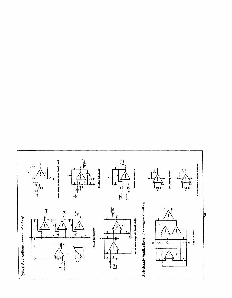
viv ► r wo¬
rn c o « o
O. < o '5. >.
vw> |»
^^ |h
"¥
w c o © O "5. Q. < Q. Q. 3 Ui
Q. (0
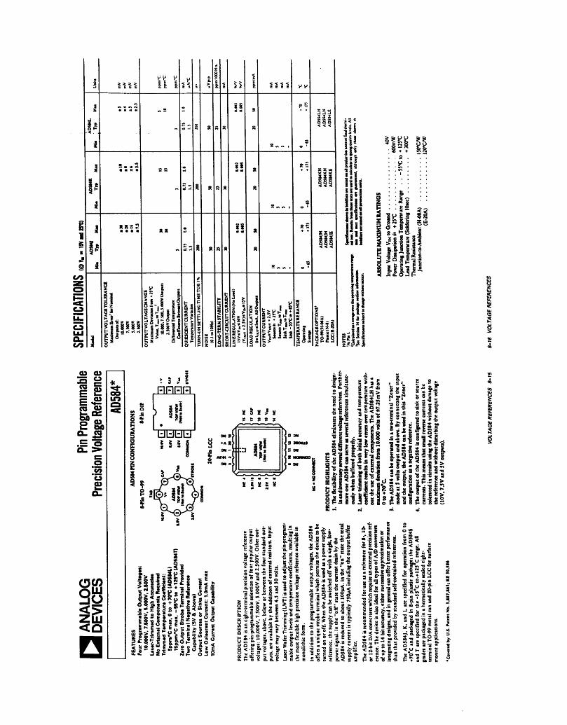
oo
C9
a. oo
t' y
iJ-.i M £ I"
oh* t E J o
il
i Mi
II
88
ss
< < < <
I Z ui X * u iii S S S < < <
ii
$ s S»- I * g 2 a s H* s 2 ♦ * is.S 3r •t *!
iUIii Q O Ml
I 2 M
SSS < < <
uiz z *5 O « 1 H < * » n
JlifiJ t 8. i E 5 &
I2ijl|
labl
e en
ce
3r t: »- OO
E^ m ^3
rogr
a ge
Re
**
o. js .E o CL. >
c= o <o o o 1— Q.
So ^> ZUJ
FIRFin
x 5 s >* 2
s-8 >>. li S 8"s.* 8!i
_- » o a •? K g
o JS * -fi 2 < •-
••sills
o s o «, - = s ** "■ o ■* TJ « « S '= S ". c *• t .2 a § « .sc.a 3 ^
"^ E-S |S S:g- £"0 3 K 8.3 3 S
- .5 = 8 S 8
E u .2 § " JO 8 i ss a a"s j; o c 3 .50-0 .= <l.s|l
u -• c a J7 H o 6 6 .S
c — m
O
JS< „
1 - § * 1 B — a» ••
•2 S.* S3 "S .2 2 >> c <! « u ^ a. W O.U\ O M
2 p. « I S * «o ■£ -= c
_1 c >. « g -» — £ <= — c "2 - 2 -
:-iiiM w 'S ^ o^ — TT1 ^ O. ■• A .2 i -r, « OL o ■=
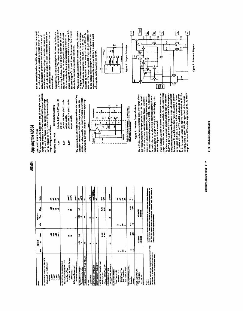
5 i* — ° - 2
■£ - JZ w '5 ii
•i o E • 2 ■0 "3 K-2 S.
s 1 i
i^ 6 ■OS —
HI U * ^ SPt u
§ 5 c J5 2 5 | 8
s
0 3-
■S -o -o C
« o "3 ° u 5 c s*-0 c-:
a «> S 5 !! 2 K *-
c - u 9 fl 3 7! ••
is 2'2 2 » o c 2^1 - s -5 0
3 — U ** o « c >.
2-S s a > tt E «. 3 0 3^»
*So- s " 2 1 S S
S o 9
8 S-S
8
- - J= ♦ -
s a s s u a <« 8 2
0 la" a u-S 3 g
' S- H 1 9" 2 -I* 8- s c <~ » 2 Jul
c « - 3 "Sao ■S 1 J-S
5 g> H I u-o 'S 2 g > g -. g -2 E > E " g "
■S-S-Zui 2 6 £-■0
Q Q
bo82^~-H^ oj-j -osSo^
■ „ u 2 - % 5 £ =3 S-" S o ^ 2 5 5 o u B j" •• "l u
1 S5T, uj * ? 5 u. w 3 g £ 3 8 >"SH-8fi8-3!5
s m o «c a> j= ♦^ t>IJ
S g.g.S «»-5 » C
|2g8 ^ S -o >.
"Si 12: ■g = : s
S e-Z 2 >o 2 2 «• a."5"" <'« S"2 S 2 w — ■£ u ~ c E Srlit » S- H - ^^ 5 g1 O S = _ -o -5 S *ile|
% -s S - ae < S < o. E D.
1*
5 > -iS^S On u -^ u w
5 •££ .S-S.S
^sa sag
H »•* *A
I ill •sl-s • - w C 9 2-s eh ^ 2'E 1
1 s-s:-s u 3 - £• 5 3 a-c U Z 3
J B £ us ■ C S .2
* 2 -«= I Ml Ho? 9 u « .E .1-a s i ? := S Si *3 Q 2 P^ < Q.
oo
1 l^%% tu il I
1
1 li 1 1111 vv
1
i
« « « « = R 2
e - s 8 «*• St
!!
8
a.8n
5£
il
1 « M « «
R^ d — § a s a
si
8
s«8-
as * * X Ul
as < <
1 i lis
Ill
il| US Ml
1^4
2 - .* =2 2 2 2- S f c SS-g g 55 § | > S * 3 S S s -1 -1s I 8 „ z * !• 3 0.
o8|52|| o i" 0 s 8 H."? £ ISIS*" .8 S«-2r 8 s-i^.
s 11 ] E a ^ •? i ■3 sS-s> c 1J - SSugMg^a 2 a "a - 5 & S fr O 5 2 If o S •• "©.Sg^jOuc v-" t u S .2 & 2
15 8 S -s f -e i?-g
82 8 I I 58* ill s
S3 8jg V O « •*
i< 8 5
cjsteg 111 ii
iki
■i—w^-
i "Xf
S: > a. s
6 IWllfi i
%&
ii
2 si e 2 « g.5 ■8 6 .& 8 2 •■ g
8^818.1*?
■? ■" -g 5 ? 2 3
* * t ^ 8- 2 8 g 2 5 § & g §• J! g. s w < .5 ^ -s U. 0 * 0 a ss S.s3 S.-&S.
1 & Q >
1 1 Ui
ci tt: Uj
5 O * s
^ £

z o o l>
OC u> UO i0
^I=iii'i^2i8 Sfilijsii^ ^s ^
P-S
S-3 &£-a-5-8 2x2

2
—I U3 m oo ^r o» .-= c s CM g O* 5 *» K RJ^S co ^, en
to s o g^S 38-K CSI CM CSI OJ CM CM SSs CM CM
s Ss CM CM g-i
S tcr c. c o 0 0 0 0 c. «> 5 «-» 3 eo OO "r "* eo eo "* "* "•
-^< ^ rf» *r» •c» •rt @£ *r» 0 0 0 0
■""*
• T3 JJJ eD 0 0 "" ^ . CM
SS SS o O SS OO o c o
TO -^ ro -^ en — —* CO — CO — —
i^s °S ss s s ss ss CO s s 2 -i cvi -^ CM o —* e* —* CM o o
s
1 l/> ^
a £j!iz 32 22 ««• CD e> -J s 2 CM
^s C3 C3 O O C3 IS O 13 o o o ooo o oo o o ^ O CD
5 s m v> ui m •n tn u> m wi an wi an •rt in in «rt ^* ™* ^*
i B -f s ssgs S2S8 2S22 ^^ m ^ ^ do-i— S2S8 S2SS d c» — 3SS2 2S2
£ o
2 I I-r ass S SiCSS SiCiCS ssss sgs s SSSS S«JSS 8SSS SSS
+ -* —. « _ ll
^ s 5? s s s S s S s ti J
!£ ^^ o o s O "* 5
iS8s
o o o o o o o o o •n •n ■n •n •ci *n m •ri wi
f^ ac Ags s s s •«
CO s <3 •rt s
i^ 3 oe ,_ s _- .^ i _ CM
g s r; A Z s s ^ o s S s us <A
.rvi_ _rviJ Tdnnrtrtrtrbrtr SCBQtn
ixr LA]
ndcrtrbrtrtnzr
o sssis
>- 2 <
O tt & g
= 1 tf)
Q <
O
IrnzTTzTtrbrbTbr
JSLHJsLRJiLR-PLa ^ixrixr1
ISlpg rvi fVl
s 4 -1599
IggH
*» M o a.
? * 15 z j- i. o a, ♦i ii r/i JL, S " • o S S M e S c t» 'S G M O C ** S > -a ■o _ O c § § "o «•
P S s " S ». a.
co « ,0 • HI u <_ o
O "> g> - < o •= Z
sa 1S "
■i-s 5
■* aa ti — «o Sf io •>« 2 c 5 .5
•sil E— o « 3 ** O
<~ U U U /= - sr s •nog
u o 0" O 9- 3 c _ E < •■= «o
ii •Sc
5* 18 it 3 O *" C *» •— t* c J! o
M C .n c 3-§
1 S=££ + + s s
Irt VF z
i 1 1 CM
+ s ' 3 s -^ . : s « a •■ •—' 3 11^1 i
ach
Tf
otal
Pi
Ran
ge
nge.
T
a ^fc s<S of 2 *•
ca
ipat
ion,
Tem
pera
mpe
ratu
•S ^ •* m
a
W*
« A e JS .2 o
eg >» * S 0 « S & o §•3 |o-S.S
Ss^as
■a .a Ele
ctri
c ic
ondu
c m
brok
e ew
Ham
3)
224-
1
o S « g cu 2 S
■BH g^s-g 3a o.s 8
H •o 5 o e co
OU cu


>>>>>S<JOOOC> coinminto E^n^s^^o
•■HuioCMi^mo® o — o — " ^
■ . IO O — l
§ s
CI U> IO " io r^
§ M M
fl
2 a.
82 S o
E E S S
1 ". B B . I 1 * __ s
> S 8
rf § a 8^ a ? s 5 # e "5 * 2 s S 2 -s * ; s « * I 2?lit If : I "S .? I § g J o
Si
o 5
I s
1 s
.2 .2 u ^ e CO ID 5 * -
ii 3 3
s ? • • a a a I E E I TJ "O ^
£
i I ! 1 ! 1
CO I- z UJ
I m;
< X UJ t-
3> z u
t X J -1
8 g J X X
(0 Z td
Si
< x UJ
< »- LL. —
OC = UJ O
cc ,- _
-^ 5 S . o ? S
& '1 o -g a ■ g t-g ^ «« SlSf § <? 5 > > ■■i'JjOo r c c «>o<cS> 2 6E ^sc ._|o«» ■* cc OiO *rMC3_l • £ t CT-O"5'-'-1 ^ OO
io « "- 3 O O o = = -s 2 c m Q g ^ 3 E _• o r E t 2 S
S .1 .1 ? E • E S « E 8
* > «t
jt tn in as
•J^ OC 3
«t in 53 ^ r^ in •— UJ 2 OC 111
IT, 2s
m ~ BC 5 9P CO UJ a. w^->
.^•ui a *= o
535* in co UJ z .as ut e — ^ ^'-' C/9 «- UJ m r* a. r^< >-Za
If I!
-5 85*
6 f i
>" *
! ! 5 •
u 6
P: S
> > u> >«
8B§< > > > K
II
(ti t- Z UJ
a «5
(0" < X u
A-a6a»|OA WdinQ-OA
'f* Ui 2 •* tc ^ •— UJ
5S> £z uj ac co CJ <o UJ
•*2 UJ
^ •" a mr- m z zco CO . .e
?£ in in r* mZ zco co CO UJ Ob >-
!« > > > > > 1 4 a 1 t > 1 11
8 5 '- d d d - — w 1 f 88 8 % sss; > p 0 « 8 3 s ?
1
> ^ «) m c u> « 58 fc «- ti
8 z — N » n ■
• 5 X ri
? > s 3 > > .
«! •
11 P
u
a -1
d
w
ri
X .fc O ■ c is >
E 8
> >" E 8
> E 8
> ■o 5 1
1 *
e e > > 3 3
S 0 ^ 1 < > 8 >?1 ;%<
c : > s
> >. •• > > > >" >
Y* LT J ■
!. 2 ■ CD ■n r» > O d 0 ^ •»« ? ? "8 3 c> fi in
P ^ 0 0
J X X -1 j j add a d i a a > 9 > « > «. r > > > > > > -ooc
> > > s J> >
5J II "5 0 . , 1 f
« I 5 g i 15
5 1 = * sis* l i 5? i ifi ii iif 7
w u |-i oc L> U O -1
!H •- U) > — £ i 0 1 s s & i g *
0 0
.5 "S S? 1 < r - II l i 5 5
el M c - if • 1 » " in 2 > 5 5? ? 5 ? ? S ■£ E -3 ? 5 • 5 ^ 2 .
5 b *I1 tl i • t 1 il 111% * 1 ii ii Hi
1 -1 1 -1 1 x E
2» 0 > 3 G Xf, X -1 « in > > E =! 0 > > > 0 > > ?r
x J a MOO 3 0 O
1- z ? 3
E
1 S
z I
3
R tf)
m
i & u.
i J
i ! 10
_l O
(0
z u
h. s 1!
*"~z
OT" < X Ul
o O •> O a> > '5 s

^- ^ -4+ -— ^_ =; J
ac - - c «
-^msA N—WO '0A
in in
t in
CO
*^> . «* UJ
•~ S oe in Z "■ m co UJ Z .z CO ^ ->
co?^ UJ m -J ^ r*i <
< a
o 2 < U
< K »- U. """ O in —1 ^—^—^^ ^—^—^
< X Ul _ _
55So ^ n 2 R —
0 ? > .b E **
■2 3
I? o 1 „ TJ
I* o l-
i:
ii O u
ii
1! •5 11
=: , WM =« v,A c t «Oi ' m S ol- -■ «
.•: M M i . . :,v " V ^ $ i*^ * / /
V — —/■'
: !> — — /1 • / ' o<
/ ^_ / h. S
//nrtiii
*HW-*3«»nb»jj-|
€^5
III M 5 fc
OT I- Z u
s s OT" < X UJ
_r en CO 2 ** oc V a— UJ
2Z m z co o CO uj
^t2 UJ 7Z *** st
•- in ■■ mz zco CO .
«=. m in r^ mZ zco CO
CO
OT H Z UJ
So 3wi
Es r-c
zs OT" < X u
-co to 5 * OC
5S> »5z UJ Zco CJ to UJ
^ 2 UJ ss z in 2 **^ z co CO —i
< rr * a «» a- fa •- in mr- ins
^ Zco CO < .e Q
Omt Z * T o «i in
$ mr-. inz zco _l CO 8: CO < UJ -i
OT I- Z UJ
So
£« r"o MS
~~z OT" < X u H

> & o u 5 eS8
V
V
CO
CD UJ a. co
.I >.$
.5.S
3 8
5S s
< < < "i E i » 1
£ If' ts
i
J E 1 i E / E / h.-A I ll 1111 ^v
1 - 2 o ,3,| I : 5?
3
fjf g;s s c s I
1 2.8^ S5
1 : 5 = I- SS
£
l^ §;g3 t s s <
1 2.8. ss
i X 5 . .3.8 12 52
m
P SSS! It s * <
i 2.8. ss
> 31 ii B^ e il 5. 1
i"6
H 3 „ 5
I
i i 5
= 3 :-• y c H"" O IM g. U
SO ♦ g "3 o - l-««
^> sil u Si 8. § S
■S J " E
S E

to. S 5-5-2
li c E
Hi lor HI .9 2 3
8.ao*.aSpc|-S2.E ■£5 20SSE>2S-53o- :5 sus-l^a^o i-s is0-. M g? IfH-l 3«>ao."Ec9*-.3.2«
fr S -S . « S S e 8 •S52 5-'a §=§.!- S:
■o"c22i-sss^
aS-sl^gcsgp-S
Isnsiiii? 3 * *
::-^-:j:::ffi ■ 7 ■■!- j-—t-
ffTOK'ttfl i ._ ^ 1 — — ^
MM
I I 5
u il
-rl V - — -■
i
\ \- A \ \
' i \ \
rfeM l-"S|iS "8 Is Z ■o." * g
gills
»• O C W .
11 IK
.5-2 g S S
•?Si = g -iil.l3-2 ^ •€ .1 .?Js = e 2 « 3 «= TJ ^ -g
.- fr ; a g & s | r 5 ^ S § * 5 3 S w"S U
le v S * S-E
ago o . •»» - E
5«■j"8 i
< K £ i r-
< 8 ll" skills-
e o* g
.5 s E fr e 2 £ •- -a « « c
^ s - -a ■ » S •• ii E 2
111
* J g
IH MB l|l
«l *• 4J ** JS "O MO
o ^ U £
-5 3 o g
,8 E7-S
»8 ■S" -9-6
t 5 J " - i « 6." -S 5 g
S ii
£ i- H E.
I I 3 t % o
- o •• w
S -s « 9 2 o o r & u.i -g
I Mill -Vf «• « «i ]•
-S -a = . c o- _ S ■ •> £ e "8 - » « B
a 3 .e -; ^^ a E E c = «»■ Cs •= o s „ o a -o o « c E E j t g 2
lllil u ^ -ts *• a 5 w an M •-*
II ■o -a
I! n
il JL2
Si
ii « & . •■ .9 Q
s:8 -slv :l>-7
•n -a E i i i
JI
3 Sl&.SgTJi 5 0 0.= s « g - •" t81S1-io •• W -S ^ S = t C
Ui ili'n '' i1 il
§ s s ■o — >.
lis 1*8 •&
111 ifl 88 - ■§ S 3
6-S •S - •< •c M rs o
!' "■ I! j
f. a-g-J
c 2 * o
=3 g-SJ
g-38 i
. E u 8 i>8-s a &
<S * J; .2 >..s >»
c a s J E S"!
S S.2: -"S R ? s .fr-S § .1S a - g""? "= "S < 5
■5 1 I f 3 &£ s g -s £ s g s
S ■£ g 2 > S
8-5 H* 3 ^'lllg
o S <
§§§ .^
0 ——ytf y I MWi 1 MO a VM> «
L%i 1 TT
0 -fV
-^v
-I-2
Ul -o .
" si ui 5 9 o: -o < ui --* H 6 c * e r > 1 g III ** :3 w
"" "- "o Z^X O « o
81: §£1
o £ e S. s s s c - B E c * S S 2 S g " MS •- *; f ft- E •• 2 S |-s 3 5. ?
,2 <* •• P s o's o o> „ £ ^v* *" •• Z£ E1 E-3 o 2 — — a o. > " £• i- a'0
2 u
Ho 921' -l-aSaal
8 8 - +. O r- *» • S O aa c -J
g .§ -s g j as E s/s iH § -s 5
o _ 2 0 3 (i S S- >, o. c S--x o V E frm n J= a. g o. -5 -
« 2SSa| H o pic o 5
e,:isS.-s« 8 U " 2 — "2
" S KOI
E-fi 5^8
- -a H g .5 ? o. * 0.0 J- * C o
s 55
"S 'i "2 B-g fr- 5 ._„ *-330s«in.a-S si r^ si's .si* 3»2.-
Ug-'S j-S'S"-g^-g §
= «s':-'§g«E-!stS
iiJiin*iii!iH- 5 T» t -s 5 s H
fr
I •5 " - it F sSi>&8£o|S r-a-? . .t S o o g -G 5 . S i! «■
2^S8:.9-3-
|S=<^-ajj2-5 ;tsoocogs I ■£ v * S-2 » -2 S
II go 2 g-S « E
>',osoSjj«"'g
■ ^lYKlfsSS s-if
54lililll
3 fr -111 I?
-& -J *
B - « g I v o « -9 g •1 " 5 P s ■S -o -c c c ' = ■8 i-l os a. 5 ^ •£
= C E .S> 8 ~ s 3
|H fill 2 i- 2 -g 2 ? — ? 315 5 i-i g ^ Sc-s ■g1-:8.a X ■• o.^ „ o g >, Z - S.H a.C g g
SSSsss-sfS 0< c .0 -5 u. C •— C
SSH-S 82 2 S-fs
.a £ S.2 " •- x o.1- g - Q s -o
SJ -■S o'it-S fr 2 § s-U-g-s-s >>i«hOOL.O— uo- C.-<>3-eo.-!« < O ^ 1. - - — 3 •* "" «i
Zs *r §1 s s--s
8i3ile 5 -3

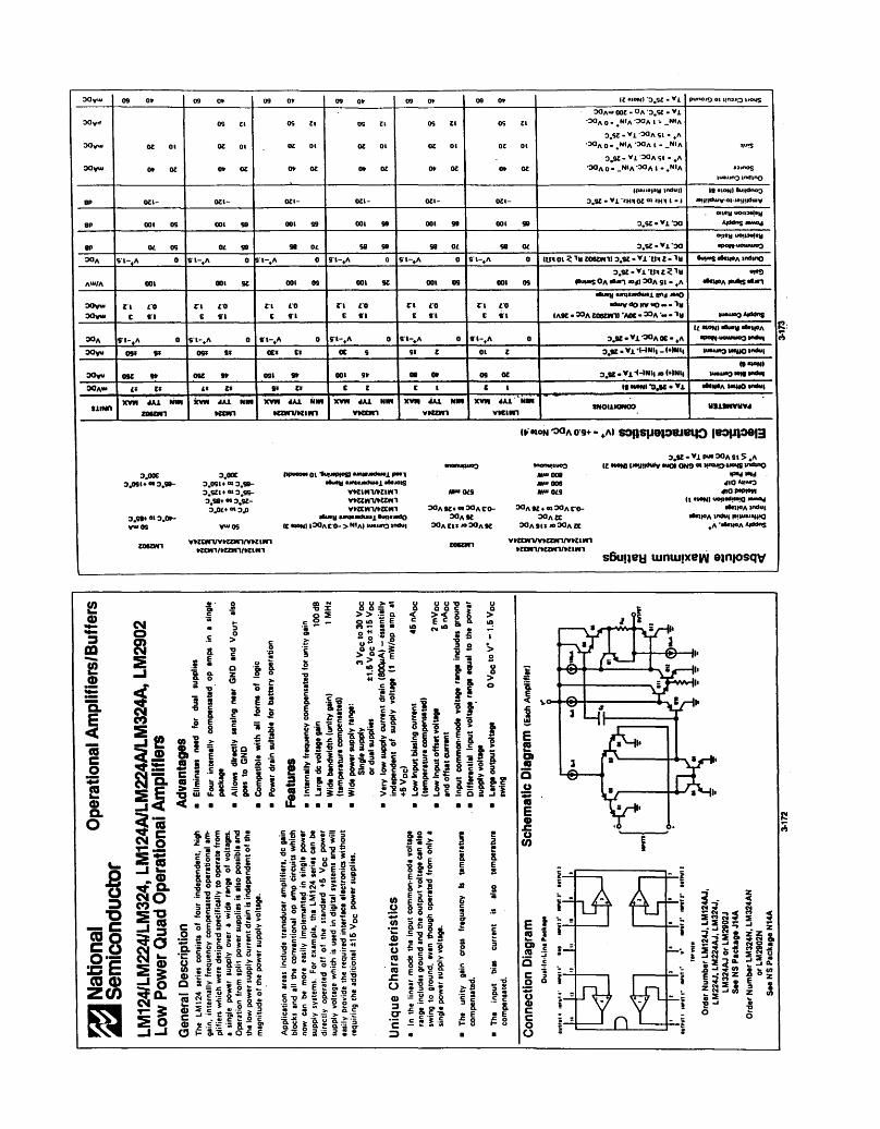
OOyul 09 0» | 09 0> 09 Of 1 09 0* 09 - 1 09 0» | (Z MONI 3.9Z - vl punoiO oi IIIUII.O IIOMS
DOvK
DO vui
Oi
0»
01
oz
OS II
02 Ot
0» 01
OS
oz
0»
tl
01
oz
OS li
OZ 01
o» oz
09 Zl
OZ 01
0* oz
09
OZ
oa
Zl
01
OZ
OOf.m OOZ - OA O.SZ - Vx
•30A 0 . tNIA DOA I - _NIA
D.9Z - Vx MA 91 - ,A
'^A 0 ■ /"A OOA I - _NI A
3.SZ - Vl OOA Sl - ,A
•3<lA0-_NlA-3OAl.,NlA
>|U'S
»inos
iu«ijn3 indinQ
8P Ml- OZl- 011- ozi- OZI- ozi-
|paiM|a)j indui)
3.SZ - *! ''m OZ « IHH I - 1
18 MONI lujldnoo
j«|i|duiv^>|.|«t!|duiv
8P 001 OS 001 S9 001 S9 001 99 001 99 001 99 3.SZ - Vx 30
oi»u uotlMtou
Aiddns JMMrf
8P 01 OS 01 99 se 01 58 99 ss ot SS Ot 3.SZ.VX-30
OIIIU uoiiMfau
3<JA Sl-.A 0 Sl%A 0 Sl-^A 0 8I-»A 0 Sl-+A o 9-l-+A 0 •III 01 Z iM Z06ZW-I) 3.SZ - *1 Ul Z - iM Bw-is^ntOAindmo
AUI/A 001 001 SZ 001 OS 001 SZ 001 OS 001 09
s.sz-^i'uiz^iu (6uiMS OA ••iai JOj| SOA 91 - tA
utao
rtat|OAiau9|saljn
aoyw
DOyui
ri to C VI
rt to t 91 C VI
ri to
C 91 c ro 9-1
ri ro c 9-1
rtuau aintajaduiax Itnj ja«o
•*uV<«OIIV«JO--"»«
IA9Z • 33A ZOOZM-H *A0C • 33A'-• iH IU.JJCO Aiddns
OOA 9-1-.A 0 9l-tA 0 «• IV* 0 S-l-.A 0 8-l-tA 0 ffl-+A 0 3.9Z->'l,3aA0C-»A
tt aWNI lauaii aaai^A
5 DOyu OW 9» 09» 8* OCT t* OC 9 SI t 01 I 3^Z.Vx'MNI,.UMl| luaijno wauo »"*»!
DOyu OK 9t osz m 091 S» 001 St 00 oa 09 OZ 3.9Z.VX(-»NI|JO(+INI|
WaMNI
luainQMiflindui
OOAUI « l» tt tf 9* » c z 1 c . C 1 l9«aNI'3.K.Vx a9ai|«A MMO mdui
txmn XVN JA1
ZOKMI
Nm XVN JA1 NM
KCNl
XVN Mi NIM
Mzm/Kun XVN 4A1 NIM
vwon XVN 4A1 NM
V»tZNl
XVN 4KL Htm
VKIN1 SNOI1ION03 M113NVUVJ
12 ©
3 CQ
E < CO c o i a S 0) Q. o
£ o
■=: c (0 o
s E CD 0) zco
CM o
i 5.
_E I3<
CMQ
. CO
SB
3 §
5 5=- >> 5 ft O m c t n — fi <a
>^,< E
> < E ?
J? o
i 2 £ o - 2 £ 5
GO "$ 3
f 2 • .£ 1° l s £ •? : * is ~ ' •g a £ a < §. 3 < ■ ■ ■ ■
« 1 i ^
«> 8 S ** S c
S* E 3« I S i
53!
fi ?!
i .nniii
f 8 11 ft & o. >«. il
-.11 !> I ifSl
■E • 2 * • -
il S Q
.9- i C o o " CA s
Q S — •o- « 2
1=loll
5 5 I « 8 f S ay a ™ *
o E &- g-o >
& O S t 5
'.a
Mil ■as o^ * 8
II & o
8= ss C -■ TJ oi
ai W O 3
s&
S .2 si
tils- s* *o
•- OI m * ■ — . u c 2 o c c — '5 S. • 0" Si. -o-E E
s ^
s " — ^. « 6 0 -S
* "s E £ n
| S c > 0 § 25 3 >• ■= >
* o- S o- ? o. £ a 03.-- c » -o
?5 €8 -O £ 11 :
a c
■a 2 P s 3 1 f
O 0)
3
8.? R 5 c .E c • 3 8. & S £0 £0
< vo--^
E S o» a a o "5 E o £ U
E I 2 I .S 2 a i
Il o <D c c o o
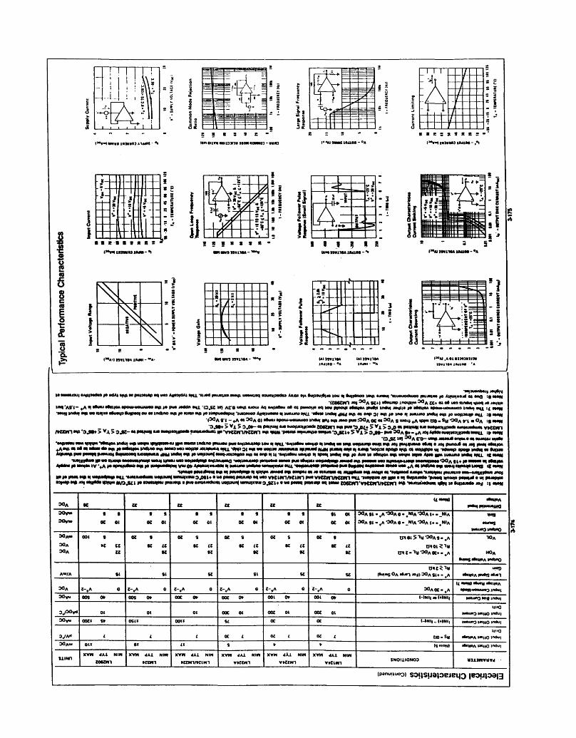
c 2 I a
mm ^T&\
I c
= r^= m L '1 i
J It f- A 1 A / / \ t
i-i 1 _ t ' i
* _...
n
V
1.
s -*> _
T
H»I einm aaiuxin loom amwo] - aum
i i M
I' *AI sauis iiMina - "A
sassassss
l~»-i Miaaai UMIM - ,*i
Hi -i , yyr. ^
rtfe "li
-^-^ «• « .». ^ "«" / s^
i!
I * * ? I III i
A •-♦
/ \ i^ 1
LJ r.
1 V) •c T5 S «0 J= O
s c ID
O t:
CO jj Q.
■ KISSXSS
i*S^ inaiiM HUM - ■■ * » a i s i ■
■n anu M«IIM - ■"•"a 3 I I J| S 2
UM naiiM UMiaa - •»
" & _ S
s u
s i 5;
('•AI MVIIM uuiaa - •*
X <
s *
. 2 i i zitizzzz c Jr 1 f i \
8 S
1 . 1 |||<| | MI
tl rf"> -^ I
3 B 1
("•A'I »vnaA IAMI - ""Ai NM imra »»IIOA - ,~>» i^Ai.AaiaiMiaMm lavnaA iiuina TA
•aaiauanbajt janBui
•(Z06ZN1 »! OQA 9Z*I aaauiap inomiM OOyy ttt o, oe uaa nndm ipoq JO jamia
-»iif|V>dU(a<pMtU|xaa6iM<ptu|pao|Ouea>n«iwa<0joa)auai0^iuapijadapu)->^^ .9mm
_w _ '9^»4'>>'X>3J>»-«PM|W!|aja«ua|wa|||3adi206tm«M>PW'9JB<«>Vl>3^««pai|«Wajaauo|ta9|||aa*
•» ^Z "1 ^A CO- "a"* JaiawO an|M • at MIMMJ iqalo •aimaau aaM ipmM 'a6ai^A tndu) aw IMHM iniqaia»«i MM aama indino tauuou pua aAOMuiMp iou * aNi-aAfwaau UOAHI a| indiq ia tasi Miwinp ai^ aia iO| |a*|4UMO a6ja| a jot puno^ o» JO) |aAa| a6at|0A ^am ot ol a« (*M tfo am |e aaOano* mdwo a* aams uaa noma JomauaA mi •** Ot "H »o uopso jou<auu mtmmd mn tumat aapaiaiain'uotuaapoipiw oi Mwppaui-aduiapapoptMfciiaa tunaa
30A K zt CC Zt Zt zc U-m —VA
30V«u
30vui • •
OZ 01
t 9
OC 01
9 9
OZ 01
1 9
OZ 01
1 9
OZ ot
•1 Oi
OZ ot
30A SI • .A "SOA 0 - /^A '30A »♦ - _NIA
30A 91 - ,A -SOA 0 - _NlA -SOA 1* - /MA •uws MMunO mdrno
DOAU.
SOA
30A
001 9
»Z CZ ZZ
OZ s
K ZZ 9Z
OZ 9
9Z ll M
OZ 9
oz zz K
OZ s
K ZZ K
OZ 9
K ZZ 9Z
in 01 > "In "SO A 9-, A
UIOl^lM inZ-lyOOAOC^-.A
■WA
HOA
•uMi$a6ti|OAind|iio
AUI/A 91 91 SZ Sl SZ SZ mt<iu
(IWMS OA aein JOJI 30A SU - tA u«
aaniOA l>i*s •to-i
3aA Z-^A 0 Z-»A 0 Z-.A 0 Z%A 0 Z-,A 0 Z-tA 0 3OA0C.+A IZ awM Kuau *ai|OA
■pawumuuiajindui SOyu 009 0» 009 0* OOC 0* OOZ 0» 001 0» 001 0* I-)NI|JO(*INI| MMJMO nig indu)
O^SOyd Ot 01 01 OOC 01 OOZ 01 OOZ 01 HMO
waunaiMMOindui 30yu OOZ? s» 09 U oou « OC OC (-|NI| - (<INI| lu>iin3 l»i)|0 indu)
OJA* I I I OC I OZ I OZ t uo-s« UfO
"•maA i-MO l"du| 00** ou Of If s * » (S »l°Nl ••niOA —HtO mdui
UINO XVN 4AX NIM XVM dAX NIM
»ZCM-l
XVM 4AI NIM
>ZZN1/»ZIW1
XVM 4A1 NIM
VtZCMl
XVM 4k± NIM
V»ZZM1
XVM 4X1 NIM
vaziMi SNOIIIONOO H31]MVliVJ -

(0 c o « o OL O. <
a. a. at 9 o> c V)
"3 o Q.
11
8? ♦-/'"-•-^AAi-fll
i—r
i—i

M e o
| Q. OU <
& 3
Ol c tn m o a.
i^/l «!i -^WV-Ill
"ii Sf Z*!-^!
ii n .-I- 03
~L<?H.
to C O «5 SS o
Q. < >» CL 3 (0 4 CD C
(JO
t—
I In|:[ 1 =«|:8rf;
-I L—MWSr-Jli
% '*
T 1

f
w c o « o
Q. < a. a. a w i o
CO
Ti o Q.
11
il ll < 3
M
Lm
^5 tU^(H" l=F=i zS

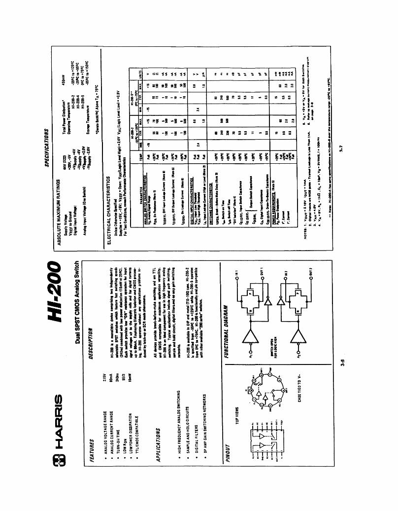
o o S <J u> m o tn
S e 11 = B S.
li
^1^
o. a. & o.
iiii
o z g cc
s 3 Z X < s iu > s
H
i £ e
i i i 1
■a "-B 1
x
_■ *
ll g ii OC •-•£
I— ""^
^ l"l
< € ■ o
OC So.'-
4*
ec -it %% %;
T S§ S§ S§ S§
* S8 -1 -i -8
SS -8 -8 -§
f S? £' 2 R2 *S* K5 R2 if t
i ! i i
4» s 5 S 2 2
i s S 2 = -
§ §
sa§s22 = -S
if if 4* *• V *• g « 8 R R 8 8 % u
8 S S
a "' 2
l2|2|2
i i
I >
M ? ■ » rf
« I s« • £ •• >
11 V< > O V V
i i
0 1 0 g*
^ ^1 s % i
CO 5
iiSiS
t = f ? - » ■ i S «
s'|€| o cr s *
Itll*
2 • ? o. .
llili &- gi-i
< Sxl 9 2
^ o f
Is! L -s -3 O « "g W
• " *» i 1 IS*
—5 <-» ?
X J! £ *
•n e a n » 2S
G *
s M F-
a 0 z 0 0 3
z C3
z z 0 Z < < t? m z < a
X
Ul 1- ►- >- u z <
1- 2 ae
X 3 0
2 z 0 5
0 X
Z
s 5
. 0 > 0 a < z <
CI (3 O < 5
t- .-r 0 z cc 1-
•
z 0
£ 0
s 0
s 0
•
0 s 0
t •
s a
u- X (3 X
•
z <
z
•
•Z
< (3 a •
< 0 a. X < 0
•
S £j
I I I 11 I I
H>-71 1 1 1 i 1 1 1

§
s i
i I
2*-
-i o
S9f
1—-mm-
8 a. 3 3 3**2 taMio - aMtwnau «o
s •I
o >• -» r1
ill
il a*
i
♦
1 \ 1
\ *
\llN 1
T
\> > i 1 It
$ > i
/
/ i ^ /
[
s
niMio - awtHKail «0
ll
•ne-rT
i i
I
{P^
TT
PI
©
-Qr
o o Z UJ
-11^-4^:
T o T : iirhif
T t T
ifrhif
^—R-
a < ■» <W «M
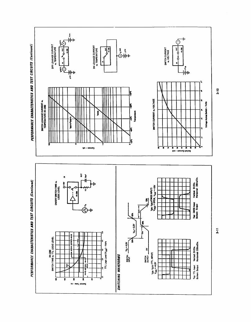
oe a =» i- u < (3 UJ
(J
CO
s i
f
^ = 8
/ -GH'lHi-
H'lH"
! >
I ... \ "x ♦
X Ul ac s *" . . . -
\
X 1 .. < ac
S i \
5 f
<? i
1 _x _ A
! \
\
a „ e * it
SSSSSXRS- yui - luajjnj ipitiws
§
1 1
I
P3J 0-+0
S a I g i i
I THVJI.
> s "1" s -i
t> C3 O 5
f y S.4 L ^
z i- / t X u 1- 1^ s / 2 *
.i < g -^
tu - aunx M5li*>S
P ♦
I 5 si
J2 S.
17^ il ^ 1.
^ <«, ■^ A
-. -> — -^
IS ii ll s - IS •• 5 o o X .. « E .. o
K 7^
<,_ Si £
II« = = ^
II
_, o t E

6.0 APPENDIX
List of Relevant NRAO Technical Reports, Memos and Reference Data
VLBA Technical Report No. 12, VLBA Standard Interface Board Manual, W. Koski and D. Weber, July 1991
VLBA Technical Report No. 1, Low Noise, 8.4 GHz, Cryogenic GASFET Front-End S. Weinreb, H. Dill, R. Harris August 1984
VLBA Technical Report No. 2, 1.5 GHz Cryogenic Front-End, R. Norrod, September 1986
VLBA Technical Report No. 3, 4.8 GHz Cryogenic Front-End, R. Norrod, December 1986
VLBA Technical Report No. 10, Model F104, 2.3 Ghz Cryogenic Front-End R. Norrod, M. Masterman, June 3, 1991
Discussion of the Front-End Monitor and Control System, VLBA Electronics Memo 41, Dick Thompson, April 1985
Vertex Room Interfacing, VLBA Electronics Memo 42, R. Norrod, April 1985
Front-End Monitor and Control, VLBA Electronics Memo 43, S. Weinreb, April 1985
Meeting on Front-End Interface, VLBA Electronics Memo 44, Dick Thompson, May 1985
Specifications:
A55001N002-A Monitor and Control Standard Interface A55001N001 Monitor and Control Bus at VLBA Stations EIA RS-485 Standard
Listing of F117 Test Program, F117_2T.BAS
65


F117 TEST PROGRAM F117_2.BAS VERSION 1/2/93
Written by Larry May
The program listed below is the F117 module test program used to test the VLBA F117 module in the AOC Front-End Laboratory. It is used in an IBM-compatible AT class PC using the C53510A007 Loop Back Test Fixture. The program was written in Microsoft BASIC.
******************************************************************************************** Program F117_2.BAS, Version 1/2/93 DEFINT A-Z •(INCLUDE: 'COMMOECL.BAS' DECLARE SUB CHECKUM () DECLARE SUB DELAY2 () DECLARE SUB SERCON () DECLARE SUB DELAY1 () DECLARE SUB CHKPRNT1 () DECLARE SUB RDMON1 () DECLARE SUB HEAD1 () DECLARE SUB SETUP1 () DIN PORTCONFIG AS ModemType DIM MONCHAR$(16, 3) DIM DIGCHAR$<&H24, 3, 16) DIM ANLGCHAR$(&H1F, 3, 16) DIM ANVAL(&H1F# 16) COMMON MONCHAR$() COMMON FLAGER1 COMMON PERERROR COMMON DLY1 CALL OpenComC'COMl: 57600,Er8>1(RB512n) IF ERR THEN PRINT "ERROR OPENING THE COM PORT" END
END IF DLY1 = 800 SUMCHECK = 0 'total test sanation flag GONO = 0 CMD = 5 'preset cryo to off for monit mode
' F117 TEST PROGRAM CLS HEAD1 ' creates main header SETUP1 ' displays setup requests
' select 117 or FE test CLS •PALETTE 0, 1 COLOR 3 PRINT "" PRINT "" PRINT "" PRINT •• PRINT •' * L.MAY 04-92 *•• PRINT •' * *" PRINT " * SELECT FOR *" PRINT " * *" PRINT " * *" PRINT " * 1 F117 MAN LOOP TEST *" PRINT " * *" PRINT " * 2 F117 AUTO LOOP TEST *" PRINT " * *" PRINT " * 3 Front End MONIT *" PRINT " * *"
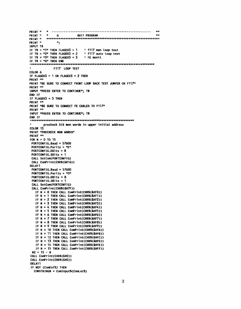
PRINT " * *" PRINT " * Q QUIT PROGRAM *» PRINT " *****************************************************************II
PRINT " "; INPUT T$ IF T$ = "1" THEN FLAGER3 =1 ' f117 man loop test IF T$ = "2" THEN FLAGER3 =2 • f117 auto loop test IF T$ = "3" THEN FLAGER3 =3 • FE monit IF T$ = "Q" THEN END i************************************************************************
• F117 LOOP TEST COLOR 6 IF FLAGER3 = 1 OR FLAGER3 = 2 THEN PRINT "" PRINT "BE SURE TO CONNECT FRONT LOOP BACK TEST JUMPER ON F117" PRINT •"• INPUT "PRESS ENTER TO CONTINUE"; T$ END IF IF FLAGER3 = 3 THEN PRINT "" PRINT "BE SURE TO CONNECT FE CABLES TO F117" PRINT "" INPUT "PRESS ENTER TO CONTINUE"; T$ END IF i************************************************************
' precheck SIB mon words in upper initial address COLOR 13 PRINT "PRECHECK MON WORDS" PRINT "" FOR N = 0 TO 15 PORTCONFIG.Baud = 57600 PORTCONFIG.Parity = "E" PORTCONFIG.DBits = 8 PORTCONFIG.SBits = 1 CALL SetCom(PORTCONFIG) CALL CoinPrint(CHR$(&Hl6))
DELAY1 PORTCONFIG.Baud = 57600 PORTCONFIG.Parity = "0" PORTCONFIG.DBitS = 8 PORTCONFIG.SBits = 1 CALL SetCom(PORTCONFIG) CALL ComPrint(CHR$(&H7F))
IF N = 0 THEN CALL ComPrint(CHR$(&HFO)) IF N = 1 THEN CALL ComPrint(CHR$(&HFl)) IF N = 2 THEN CALL ComPrint(CHR$(&HF2)) IF N = 3 THEN CALL CoinPrint(CHR$(&HF3)) IF N = 4 THEN CALL CoinPrint(CHR$(&HF4)) IF N = 5 THEN CALL ComPrint(CHR$(&HF5)) IF N = 6 THEN CALL CoinPrint(CHR$(&HF6)) IF N = 7 THEN CALL ComPrint(CHR$(&HF7)) IF N = 8 THEN CALL ComPrint(CHR$(&HF8)) IF N = 9 THEN CALL ComPrint(CHR$(&HF9)) IF N = 10 THEN CALL Coirf>rint(CHR$(&HFA)) IF N = 11 THEN CALL ComPrint(CHR$(&HFB)) IF N = 12 THEN CALL Co(T)Print(CHR$(&HFC)) IF N = 13 THEN CALL ComPrint(CHR$(&HFD)) IF N = 14 THEN CALL ComPrint(CHR$(&HFE)) IF N = 15 THEN CALL ComPrint(CHR$(&HFF))
N2 = 15 - N CALL ConiPrint(CHR$(&HO)) CALL Co<nPrint(CHR$(&HO)) DELAY1 IF NOT (ConCof%) THEN COMSTRINGS = ComInput$(ComLoc%)
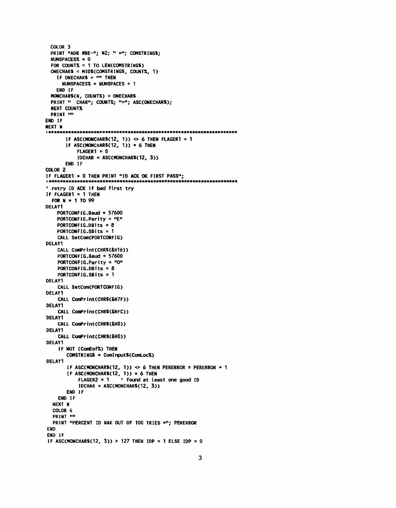
COLOR 3 PRINT "ADR #BE-"; N2; " ="; COMSTRINGS; NUMSPACESX = 0 FOR COUNTX = 1 TO LEN(COMSTRING$) ONECHARS = MIDtCCOMSTRINGS, COUNTX, 1)
IF ONECHARS = "" THEN NUMSPACESX = NUMSPACES + 1
END IF MONCHAR$(N, COUNTX) = ONECHARS PRINT " CHAR"; COUNTX; "='•; ASC(ONECHARS); NEXT COUNTX PRINT ""
END IF NEXT N i*******************************************************************
IF ASC(MONCHAR$(12, 1)) <> 6 THEN FLAGER1 = 1 IF ASC(MONCHAR$(12, 1)) = 6 THEN
FLAGER1 = 0 IDCHAR - ASC(MONCHAR$(12, 3))
END IF COLOR 2 IF FLAGER1 = 0 THEN PRINT "ID ACK OK FIRST PASS";
' retry ID ACK if bad first try IF FLAGER1 = 1 THEN
FOR N = 1 TO 99 DELAY1
PORTCONFIG.Baud = 57600 PORTCONFIG.Parity = "E" PORTCONFIG.DBitS = 8 PORTCONFIG.SBits = 1 CALL SetCom(PORTCONFIG)
DELAY1 CALL Co(nPrint(CHR$(&Hl6)) PORTCONFIG.Baud = 57600 PORTCONFIG.Parity = "0" PORTCONFIG.DBitS = 8 PORTCONFIG.SBits = 1
DELAY1 CALL SetCom(PORTCONFIG)
DELAY1 CALL ComPrint(CHR$(&H7F))
DELAY1 CALL Co<nPrint(CHR$(&HFC))
DELAY1 CALL CoinPrint(CHR$(&HO))
DELAY1 CALL CoinPrint(CHR$(&HO))
DELAY1 IF NOT (ComEofX) THEN
COMSTRINGS = ComInput$(ComLocX) DELAY1
IF ASC(MONCHAR$(12( 1)) <> 6 THEN PERERROR = PERERROR + 1 IF ASC(MONCHAR$(12, 1>) = 6 THEN
FLAGER2 = 1 ' found at least one good ID IDCHAR = ASC(MONCHAR$(12, 3))
END IF END IF
NEXT N COLOR 4 PRINT "" PRINT "PERCENT ID NAK OUT OF 100 TRIES ="; PERERROR
END END IF IF ASC(MONCHAR$(12, 3)) > 127 THEN IDP = 1 ELSE IDP = 0
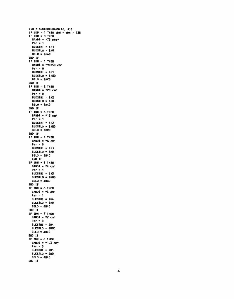
IDN = ASC(M0NCHAR$(12, 3)) IF IDP = 1 THEN IDN = IDN - 128 IF IDN = 0 THEN BANDS = "75 mHz" Par = 1 BLKSTHI = &H1 BLKSTLO = &H0 BELO = &H40
END IF IF IDN = 1 THEN BANDS = "90/50 cm" Par = 0 BLKSTHI = &H1 BLKSTLO = &H80 BELO = &HC0
END IF IF IDN s 2 THEN BANDS = "20 cm" Par = 0 BLKSTHI = &H2 BLKSTLO = &H0 BELO = &H40
END IF IF IDN s 3 THEN BANDS = "13 cm" Par = 1 BLKSTHI = &H2 BLKSTLO = &H80 BELO = &HC0
END IF IF IDN = 4 THEN BANDS = "6 cm" Par = 0 BLKSTHI = &H3 BLKSTLO = &H0 BELO = &H40 END IF
IF IDN = 5 THEN BANDS = "4 cm" Par = 1 BLKSTHI = &H3 BLKSTLO = &H80 BELO = &HC0
END IF IF IDN = 6 THEN BANDS = "3 cm" Par = 1 BLKSTHI = &H4 BLKSTLO = &H0 BELO = &H40
END IF IF IDN = 7 THEN BANDS = "2 cm" Par = 0 BLKSTHI = &H4 BLKSTLO = &H80 BELO = &HC0
END IF IF IDN = 8 THEN BANDS = "1.3 cm" Par = 0 BLKSTHI = &H5 BLKSTLO = &H0 BELO = &H40
END IF

IF IDN = 9 THEN BANDS = "7 nm" Par = 1 BLKSTHI = &H5 BLKSTLO = &H80 BELO = &HC0
END IF IF IDN = 10 THEN BANDS = "4 mm" Par = 1 BLKSTHI = &H6 BLKSTLO = &H0 BELO = &H40
END IF IF IDN > 10 THEN BANDS = "NO BAND" IF Par <> IDP THEN
COLOR 4 PRINT " ID = EVEN PARITY - BAD"
END IF IF Par = IDP THEN
COLOR 13 PRINT " ID = ODD PARITY - OK"
END IF COLOR 2 PRINT "ID PARITY = "; COLOR 13 PRINT IDP; COLOR 2 PRINT " ID VALUE = "; COLOR 13 PRINT IDN; COLOR 2 PRINT " BAND MUST BE = "; COLOR 13 PRINT BANDS IF IDN > 10 THEN END i**********************************************************
1 check all 16 char ack FLAGER1 = 0 FOR N3 = 0 TO 15 IF ASC(MONCHAR$(N3, 1)) <> 6 THEN FLAGER1 = 1 NEXT N3 IF FLAGER1 = 1 THEN
COLOR 4 PRINT "NO ACK ONE OR MORE INITIAL MON WORDS" END
END IF IF FLAGER1 = 0 THEN
COLOR 2 PRINT "ALL ACK OK FIRST PASS"
END IF ******************************************************************
• check for zeros FLAGER1 = 0 FOR N3 = 0 TO 13
FOR N4 = 2 TO 3 IF ASC(MONCHARS(N3( N4)) <> 0 AND N3 <> 5 AND N3 <> 12 THEN FLAGER1 = 1
NEXT N4 NEXT N3 IF FLAGER1 = 1 THEN COLOR 4 PRINT "ONE OR MORE MON WORDS NOT ZERO THAT SHOULD BE" END
END IF IF FLAGER1 = 0 THEN
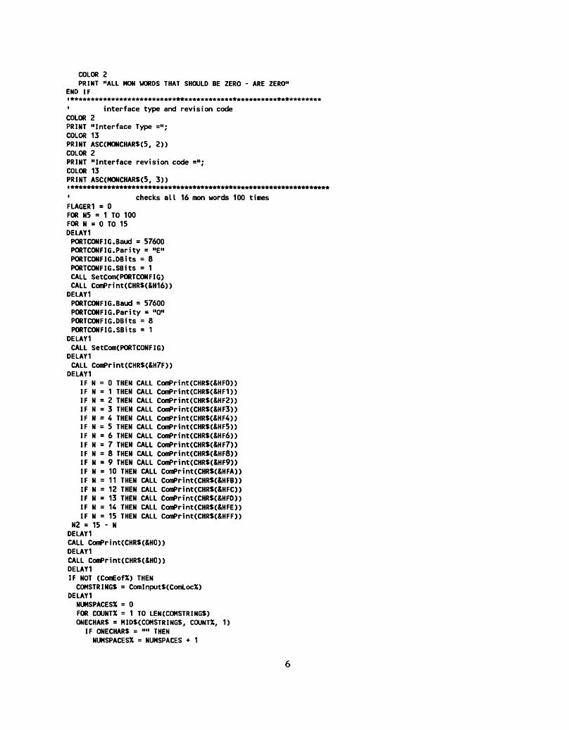
COLOR 2 PRINT "ALL MON WORDS THAT SHOULD BE ZERO - ARE ZERO"
END IF i**************************************************************
1 interface type and revision code COLOR 2 PRINT "Interface Type ="; COLOR 13 PRINT ASC<MONCHARS(5, 2)) COLOR 2 PRINT "Interface revision code ="; COLOR 13 PRINT ASC(MONCHARS(5, 3)) 1**************************************************************4
' checks all 16 mon words 100 times FLAGER1 = 0 FOR N5 = 1 TO 100 FOR N = 0 TO 15 DELAY1 PORTCONFIG.Baud = 57600 PORTCONFIG.Parity = "E" PORTCONFIG.DBitS = 8 PORTCONFIG.SBits = 1 CALL SetCom(PORTCONFIG) CALL ComPrint(CHRS(&H16))
DELAY1 PORTCONFIG.Baud = 57600 PORTCONFIG.Parity = "O" PORTCONFIG.DBitS = 8 PORTCONFIG.SBits = 1
DELAY1 CALL SetCom(PORTCONFIG)
DELAY1 CALL ComPrint(CHR$(&H7F))
DELAY1 IF N = 0 THEN CALL ComPrint(CHRS(&HFO)) IF N = 1 THEN CALL ComPrint(CHR$(&HF1)) IF N = 2 THEN CALL ComPrint(CHR$(&HF2)) IF N = 3 THEN CALL ComPrint(CHRS(&HF3)) IF N = 4 THEN CALL ConiPrint(CHR$(&HF4)) IF N = 5 THEN CALL ComPrint(CHRS(&HF5)) IF N = 6 THEN CALL ComPrint(CHRS(&HF6)) IF N = 7 THEN CALL CofnPrint(CHR$(&HF7)) IF N = 8 THEN CALL CoinPrint(CHRS(&HF8)) IF N = 9 THEN CALL ComPrint(CHR$(&HF9)) IF N = 10 THEN CALL CoinPrint(CHRS(&HFA)) IF N = 11 THEN CALL ComPrint(CHRS(&HFB)) IF N = 12 THEN CALL ComPrint(CHRS(&HFC)) IF N = 13 THEN CALL ComPrint(CHRS(&HFD)) IF N = 14 THEN CALL ComPrint(CHR$(&HFE)) IF N = 15 THEN CALL ComPrint(CHR$(&HFF))
N2 = 15 - N DELAY1 CALL ComPrint(CHRS(&HO)) DELAY1 CALL ComPrint(CHRS(&HO)) DELAY1 IF NOT (ComEofX) THEN COMSTRINGS = ComlnputS(ComLocX)
DELAY1 NUMSPACESX = 0 FOR COUNTX = 1 TO LEN(COMSTRINGS) ONECHARS = MID$(COMSTRINGS, COUNTX, 1)
IF ONECHARS = "" THEN NUMSPACESX = NUMSPACES + 1

END IF MONCHARS(N, COUNTX) = ONECHARS NEXT COUNTX
END IF NEXT N ********************************************************************
CHKPRNT1 ' checks values of monitor words & prints error message i**********************************************************
' check all 16 char ack FLAGER1 = 0 FOR N3 = 0 TO 15
IF ASC(M0NCHAR$(N3, 1)) <> 6 THEN FLAGER1 = 1 NEXT N3 IF FLAGER1 = 1 THEN
COLOR 4 PRINT "NO ACK ONE OR MORE SUBSEQUENT MON WORDS" END
END IF i*****************************************************************
' check for zeros FLAGER1 = 0 FOR N3 = 0 TO 13
FOR N4 = 2 TO 3 IF ASC(MONCHAR$(N3, N4)) <> 0 AND N3 <> 5 AND N3 <> 12 THEN FLAGER1 = 1
NEXT N4 NEXT N3 IF FLAGER1 = 1 THEN COLOR 4 PRINT "ONE OR MORE MON WORDS NOT ZERO THAT SHOULD BE" END
END IF LOCATE 24, 1 PRINT "CHECKING ALL FIRST 16 SIB MON WORDS 100 TIMES - CHECK #"; N5; NEXT N5 LOCATE 24, 1 PRINT " "; LOCATE 24, 1 COLOR 14 IF FLAGER3 = 1 THEN INPUT "SIB FIRST 16 MON WORDS LOOK OK - PRESS ENTER TO CONTINUE"; TS IF FLAGER3 = 2 OR FLAGER3 = 3 THEN PRINT "SIB FIRST 16 MON WORDS LOOK OK - PRESS ENTER TO CONTINUE"; TS
i**********************************************************************
' relocate response address of sib
• clear array FOR N = 0 TO 15
FOR COUNTX = 1 TO 3 MONCHAR$(Nf COUNTX) = "1"
NEXT COUNTX NEXT N i***********************************************
• begin repeat of initial sib test CLS PRINT "IDN ="; IDN IF IDN = 0 THEN
CADRILO = &H0 CADR2LO = &H1
END IF IF IDN = 1 THEN
CADRILO = &H2 CADR2LO = &H3
END IF IF IDN = 2 THEN
CADR1LO = &H4 CADR2LO = &H5

END IF IF IDN = 3 THEN
CADRILO = &H6 CADR2LO = &H7
END IF IF IDN = 4 THEN
CADR1LO = &H8 CADR2LO = &H9
END IF IF IDN = 5 THEN
CADRILO = &HA CADR2LO = &HB
END IF IF IDN = 6 THEN
CADRILO = &HC CADR2LO = &HD
END IF IF IDN = 7 THEN
CADRILO = &HE CADR2LO = &HF
END IF IF IDN = 8 THEN
CADRILO = &H10 CADR2LO = &H11
END IF IF IDN = 9 THEN
CADRILO = &H12 CADR2LO = &H13
END IF IF IDN = 10 THEN
CADRILO = &H14 CADR2LO = &H15
END IF PRINT "IDN ="; IDN; " CADRILO ="; CADR1LO; " CADR2LO ="; CADR2LO i****************************************************
' send new block size PRINT "" DELAY1 PORTCONFIG.Baud = 57600 PORTCONFIG.Parity = "E" PORTCONFIG.DBitS = 8 PORTCONFIG.SBits = 1 CALL SetCom(PORTCONFIG) CALL CofnPrint<CHRS<&H16))
DELAY1 PORTCONFIG.Baud = 57600 PORTCONFIG.Parity = "0" PORTCONFIG.DBitS = 8 PORTCONFIG.SBits = 1 CALL SetCom(PORTCONFIG)
DELAY1 CALL ComPrint(CHR$(&H80)) • msb of adr to load data
DELAY1 CALL ComPrint(CHR$(CADRILO)) ' Isb of adr to load data
DELAY1 CALL ComPrint(CHRS(&H0)) • msb block size
DELAY1 CALL ComPrint(CHR$(&H40)) ' Isb block size
DELAY1 DELAY1 IF NOT (ComEofX) THEN COMSTRINGS = ComInput$(ComLocX) DELAY1 COLOR 3 PRINT " BLOCK SIZE COMMAND RESPONSE ="; COMSTRINGS;

NUMSPACESX = 0 FOR COUNTX = 1 TO LEN(COMSTRINGS) ONECHARS = MID$(COMSTRINGS, COUNTX, 1)
IF ONECHARS = "" THEN NUMSPACESX = NUMSPACES + 1
END IF PRINT " CHAR"; COUNTX; » ="; ASC(ONECHAR$); NEXT COUNTX PRINT ""
END IF PRINT "JUST SENT BLOCK SIZE COMMAND" i****************************************************
' send new block start adr PRINT "" DELAY1 PORTCONFIG.Baud = 57600 PORTCONFIG.Parity = "E" PORTCONFIG.DBitS = 8 PORTCONFIG.SBits = 1 CALL SetCom(PORTCONFIG)
DELAY1 CALL CoinPrint(CHRS(&Hl6))
DELAY1 PORTCONFIG.Baud = 57600 PORTCONFIG.Parity = "0" PORTCONFIG.DBitS = 8 PORTCONFIG.SBits = 1 CALL SetCom(PORTCONFIG)
DELAY1 DELAY1 CALL ComPrint(CHRS(&H80)) • msb adr to load data
DELAY1 DELAY1 CALL ComPrint(CHRS(CADR2LO)) ' Isb adr to load data
DELAY1 DELAY1 PRINT "BLKSTHI="; BLKSTHI CALL CoinPrint(CHRS(BLKSTHI)) ' msb block start adr hi
DELAY1 DELAY1 PRINT "BLKSTLO+"; BLKSTLO CALL ComPrint(CHRS(BLKSTLO)) ' Isb block start adr lo
DELAY1 DELAY1 IF NOT (ComEofX) THEN COMSTRINGS = ComInput$(ComLocX) DELAY1 COLOR 3 PRINT "BLOCK START ADR COMMAND RESPONSE ="; COMSTRINGS; NUMSPACESX = 0 FOR COUNTX = 1 TO LEN(COMSTRINGS) ONECHARS = MIDS(COMSTRINGS, COUNTX, 1)
IF ONECHARS = "" THEN NUMSPACESX = NUMSPACES + 1
END IF PRINT " CHAR"; COUNTX; " ="; ASC(ONECHAR$); NEXT COUNTX PRINT ""
END IF i*********************************************************************
' repeat initial mon word checks at relocated address PERERROR = 0 'CLEAR ERROR COUNTER DELAY1 FOR N2 = 0 TO 15
FOR N3 = 0 TO 3

M0NCHAR$(N2, N3) = "0" NEXT N3
NEXT N2 PRINT "" PRINT " STARTING RECHECK OF RELOCATED MON WORDS" PRINT "" DELAY1
IF BELO = &H40 THEN X = 1 IF BELO = &HC0 THEN X = 2
FOR N = 0 TO 15 DELAY1 PORTCONFIG.Baud = 57600 PORTCONFIG.Parity = "E" PORTCONFIG.DBitS = 8 PORTCONFIG.SBits = 1 CALL SetCom(PORTCONFIG) CALL CoinPrint(CHRS(&Hl6))
DELAY1 PORTCONFIG.Baud = 57600 PORTCONFIG.Parity = "0" PORTCONFIG.DBitS = 8 PORTCONFIG.SBits = 1 CALL SetCom(PORTCONFIG)
DELAY1 CALL ComPrint(CHRS(BLKSTHI)) ' msb block start adr hi
DELAY1 IF N = 0 AND X = 1 THEN CALL CoinPrint(CHRS(&H30)) IF N = 0 AND X = 2 THEN CALL CofnPrint(CHR$(&HBO)) IF N = 1 AND X = 1 THEN CALL ComPrint(CHRS(&H31)) IF N = 1 AND X = 2 THEN CALL ComPrint(CHR$(&HBl)) IF N = 2 AND X = 1 THEN CALL ComPrint(CHRS(&H32)) IF N = 2 AND X = 2 THEN CALL ComPrint(CHR$(&HB2)) IF N = 3 AND X = 1 THEN CALL ComPrint(CHRS(&H33)) IF N = 3 AND X = 2 THEN CALL ComPrint(CHRS(&HB3)) IF N = 4 AND X = 1 THEN CALL ComPrint(CHRS(&H34)) IF N = 4 AND X = 2 THEN CALL ComPrint(CHR$(&HB4)) IF N = 5 AND X = 1 THEN CALL ComPrint(CHRS(&H35)) IF N = 5 AND X = 2 THEN CALL ComPrint(CHRS(&HB5)) IF N = 6 AND X = 1 THEN CALL CofnPrint(CHRS(&H36)) IF N = 6 AND X = 2 THEN CALL ComPrint(CHR$(&HB6)) IF N = 7 AND X = 1 THEN CALL ComPrint(CHRS(&H37)) IF N = 7 AND X = 2 THEN CALL ComPrint(CHR$(&HB7)) IF N = 8 AND X = 1 THEN CALL ComPrint(CHR$(&H38)) IF N = 8 AND X = 2 THEN CALL ComPrint(CHR$(&HB8)) IF N = 9 AND X = 1 THEN CALL CoinPrint(CHRS(&H39)) IF N = 9 AND X = 2 THEN CALL ComPrint(CHRS(&HB9)) IF N = 10 AND X = 1 THEN CALL CoinPrint(CHRS(&H3A)) IF N = 10 AND X = 2 THEN CALL ComPrint(CHR$(&HBA)) IF N = 11 AND X = 1 THEN CALL ComPrint(CHRS(&H3B)) IF N = 11 AND X = 2 THEN CALL ComPrint(CHRS(&HBB)) IF N = 12 AND X = 1 THEN CALL ComPrint(CHR$(&H3C)) IF N = 12 AND X = 2 THEN CALL ComPrint(CHRS(&HBC)) IF N = 13 AND X = 1 THEN CALL ComPrint(CHRS(&H3D)) IF N = 13 AND X = 2 THEN CALL ComPrint(CHRS(&HBD)) IF N = 14 AND X = 1 THEN CALL ComPrint(CHRS(&H3E)) IF N = 14 AND X = 2 THEN CALL ComPrint(CHRS(&HBE)) IF N = 15 AND X = 1 THEN CALL ComPrint(CHRS(&H3F)) IF N = 15 AND X = 2 THEN CALL ComPrint(CHRS(&HBF))
N2 = 15 - N DELAY1 CALL ComPrint(CHRS(&H0)) DELAY1 CALL ComPrint(CHRS(&H0)) DELAY1 IF NOT (ComEofX) THEN
10

COMSTRINGS = ComlnputS(CofnLocX) COLOR 3 PRINT "ADR #BE-"; N2; " ="; COMSTRINGS; NUMSPACESX = 0 FOR COUNTX = 1 TO LEN(COMSTRINGS) ONECHARS = MID$(COMSTRINGS, COUNTX, 1)
IF ONECHARS = "" THEN NUMSPACESX = NUMSPACES + 1
END IF MONCHAR$(N, COUNTX) = ONECHARS PRINT " CHAR"; COUNTX; "="; ASC(ONECHARS); NEXT COUNTX PRINT ""
END IF NEXT N
IF ASC(MONCHARS(12, 1)) <> 6 THEN FLAGER1 = 1 IF ASC(MONCHARS(12, 1)) = 6 THEN
FLAGER1 = 0 IDCHAR = ASC(MONCHARS(12, 3))
END IF COLOR 2 IF FLAGER1 = 0 THEN PRINT "relocated ID ACK OK FIRST PASS"; i*******************************************************************
• retry ID ACK if bad first try IF FLAGER1 = 1 THEN
FOR N3 = 1 TO 99 LOCATE 20, 20 PRINT N3; MONCHARS(12, 3) = "0" FOR N = 12 TO 12 DELAY1 DELAY1
PORTCONFIG.Baud = 57600 PORTCONFIG.Parity = "E" PORTCONFIG.DBitS = 8 PORTCONFIG.SBits = 1 CALL SetCom(PORTCONFIG)
DELAY1 CALL Co<nPrint(CHRS(&H16))
DELAY1 PORTCONFIG.Baud = 57600 PORTCONFIG.Parity = "0" PORTCONFIG.DBitS = 8 PORTCONFIG.SBits = 1 CALL SetCom(PORTCONFIG)
DELAY1 CALL ComPrint(CHRS(BLKSTHI)) DELAY1
IF N = 0 AND X = 1 THEN CALL ComPrint(CHR$(&H30)): PRINT "LO ADR = &H30 OK"; N3 IF N = 0 AND X = 2 THEN CALL ComPrint(CHR$(&HBO)) IF N = 1 AND X = 1 THEN CALL ComPrint(CHRS(&H31)) IF N = 1 AND X = 2 THEN CALL ComPrint(CHRS(&HBl)) IF N = 2 AND X = 1 THEN CALL CoinPrint(CHR$(&H32)) IF N = 2 AND X = 2 THEN CALL ComPrint(CHR$(&HB2)) IF N = 3 AND X = 1 THEN CALL ComPrint(CHRS(&H33)) IF N = 3 AND X = 2 THEN CALL ComPrint(CHRS(&HB3)) IF N = 4 AND X = 1 THEN CALL ComPrint(CHRS(&H34)) IF N = 4 AND X = 2 THEN CALL CofnPrint(CHRS(&HB4)) IF N = 5 AND X = 1 THEN CALL CoinPrint(CHR$(&H35)) IF N = 5 AND X = 2 THEN CALL COfnPrint(CHRS(&HB5)) IF N = 6 AND X = 1 THEN CALL ComPrint(CHR$(&H36)) IF N = 6 AND X = 2 THEN CALL ComPrint(CHRS(&HB6)) IF N = 7 AND X = 1 THEN CALL ComPrint(CHR$(&H37)) IF N = 7 AND X = 2 THEN CALL ComPrint(CHR$(&HB7))
11
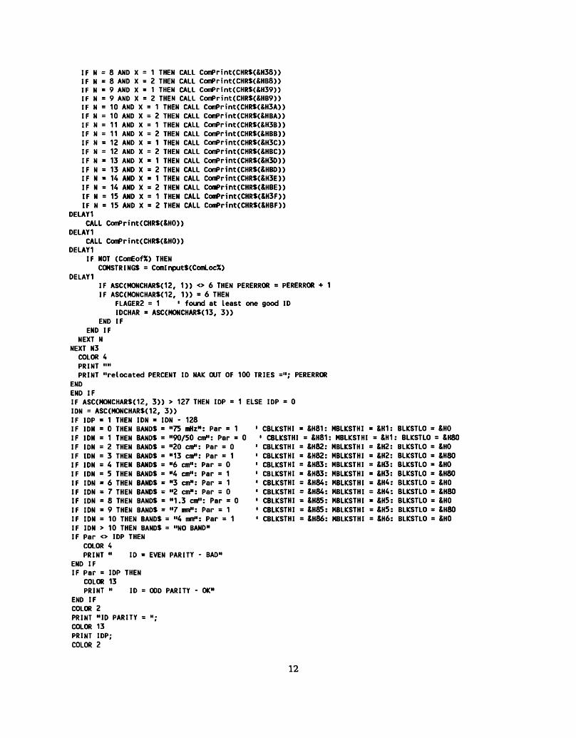
IF N IF N IF N IF N IF N IF N IF N IF N IF N IF N IF N IF N IF N IF N IF N
8 AND X = 1 THEN CALL ComPrint(CHRS(&H38)) 8 AND X = 2 THEN CALL ComPrint(CHRS(&HB8)) 9 AND X = 1 THEN CALL ComPrint(CHR$(&H39)) 9 AND X = 2 THEN CALL ComPrint(CHRS(&HB9)) 10 AND X = 1 THEN CALL ComPrint(CHRS(&H3A)) 10 AND X = 2 THEN CALL ComPrint(CHRS(&HBA)) 11 AND X = 1 THEN CALL ComPrint(CHRS(&H3B)) 11 AND X = 2 THEN CALL ConiPrint(CHR$(&HBB)) 12 AND X = 1 THEN CALL ComPrint(CHRS(&H3C)) 12 AND X = 2 THEN CALL ComPrint(CHRS(&HBC)) 13 AND X = 1 THEN CALL ComPrint(CHR$(&H3D)) 13 AND X = 2 THEN CALL ComPrint(CHRS(&HBD)) 14 AND X = 1 THEN CALL CoinPrint(CHR$(&H3E)) 14 AND X = 2 THEN CALL CoinPrint(CHR$(&HBE)) 15 AND X = 1 THEN CALL ComPrint(CHR$(&H3F)) 15 AND X = 2 THEN CALL ComPrint(CHRS(&HBF)) IF N
DELAY1 CALL ComPrint(CHRS(&HO))
DELAY1 CALL ComPrint(CHRS(&HO))
DELAY1 IF NOT (ComEofX) THEN
COMSTRINGS = ComlnputS(ComLocX) DELAY1
IF ASC(MONCHARS(12, 1)) <> 6 THEN PERERROR = PERERROR + 1 IF ASC(MONCHARS(12, 1)) = 6 THEN
FLAGER2 = 1 ' found at least one good ID IDCHAR = ASC(MONCHARS(13, 3))
END IF END IF
NEXT N NEXT N3
COLOR 4 PRINT "" PRINT "relocated PERCENT ID NAK OUT OF 100 TRIES ="; PERERROR
END END IF IF ASC(HONCHARS(12, 3)) > 127 THEN IDP = 1 ELSE IDP = 0 IDN = ASC(MONCHARS(12, 3)) IF IDP = 1 THEN IDN = IDN - 128 IF IDN = 0 THEN BANDS = "75 mHz": Par = 1 CBLKSTHI = &H81: MBLKSTHI = &H1: BLKSTLO = &H0 IF IDN = 1 THEN BANDS = "90/50 cm": Par = 0 • CBLKSTHI = &H81 : MBLKSTHI = &H1 : BLKSTLO = &H80 IF IDN = 2 THEN BANDS = "20 cm": Par = 0 CBLKSTHI = &H82: MBLKSTHI = &H2: BLKSTLO = &H0 IF IDN = 3 THEN BANDS = "13 cm": Par = 1 CBLKSTHI = &H82: MBLKSTHI = &H2: BLKSTLO = &H80 IF IDN = 4 THEN BANDS = "6 cm": Par = 0 CBLKSTHI = &H83: MBLKSTHI = &H3: BLKSTLO = &H0 IF IDN = 5 THEN BANDS = "4 cm": Par = 1 CBLKSTHI = &H83: MBLKSTHI = &H3: BLKSTLO = &H80 IF IDN = 6 THEN BANDS = "3 cm": Par = 1 CBLKSTHI = &H84: MBLKSTHI = &H4: BLKSTLO = &H0 IF IDN = 7 THEN BANDS = "2 cm": Par = 0 CBLKSTHI = &H84: MBLKSTHI = &H4: BLKSTLO = &H80 IF IDN = 8 THEN BANDS = "1.3 cm": Par = 0 CBLKSTHI = &H85: MBLKSTHI = &H5: BLKSTLO - &H0 IF IDN = 9 THEN BANDS = "7 mn": Par = 1 CBLKSTHI = &H85: MBLKSTHI = &H5: BLKSTLO = &H80 IF IDN = 10 THEN BANDS = "4 mm": Par = 1 CBLKSTHI = &H86: MBLKSTHI = &H6: BLKSTLO = &H0 IF IDN > 10 THEN BANDS = "NO BAND" IF Par <> IDP THEN
COLOR 4 PRINT " ID = EVEN PARITY - BAD"
END IF IF Par = IDP THEN
COLOR 13 PRINT " ID = ODD PARITY - OK"
END IF COLOR 2 PRINT "ID PARITY = "; COLOR 13 PRINT IDP;
12
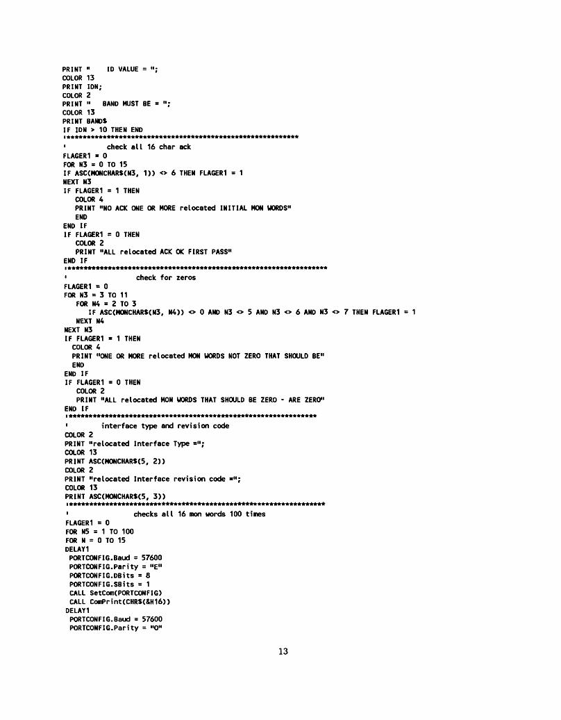
PRINT " ID VALUE = "; COLOR 13 PRINT IDN; COLOR 2 PRINT " BAND MUST BE = "; COLOR 13 PRINT BANDS IF IDN > 10 THEN END i**********************************************************
' check all 16 char ack FLAGER1 = 0 FOR N3 = 0 TO 15 IF ASC(MONCHARS(N3, 1)) <> 6 THEN FLAGER1 = 1 NEXT N3 IF FLAGER1 = 1 THEN
COLOR 4 PRINT "NO ACK ONE OR MORE relocated INITIAL MON WORDS" END
END IF IF FLAGER1 = 0 THEN
COLOR 2 PRINT "ALL relocated ACK OK FIRST PASS"
END IF
' check for zeros FLAGER1 = 0 FOR N3 = 3 TO 11
FOR N4 = 2 TO 3 IF ASC(MONCHARS(N3, N4)) <> 0 AND N3 <> 5 AND N3 <> 6 AND N3 <> 7 THEN FLAGER1 = 1
NEXT N4 NEXT N3 IF FLAGER1 = 1 THEN COLOR 4 PRINT "ONE OR MORE relocated MON WORDS NOT ZERO THAT SHOULD BE" END
END IF IF FLAGER1 = 0 THEN
COLOR 2 PRINT "ALL relocated MON WORDS THAT SHOULD BE ZERO - ARE ZERO"
END IF i**************************************************************
' interface type and revision code COLOR 2 PRINT "relocated Interface Type ="; COLOR 13 PRINT ASC(MONCHARS(5, 2)) COLOR 2 PRINT "relocated Interface revision code ="; COLOR 13 PRINT ASC(MONCHARS(5, 3))
1 checks all 16 mon words 100 times FLAGER1 = 0 FOR N5 = 1 TO 100 FOR N = 0 TO 15 DELAY1 PORTCONFIG.Baud = 57600 PORTCONFIG.Parity = "E" PORTCONFIG.DBitS = 8 PORTCONFIG.SBits = 1 CALL SetCom(PORTCONFIG) CALL ComPrint(CHR$(&Hl6))
DELAY1 PORTCONFIG.Baud = 57600 PORTCONFIG.Parity = "0"
13
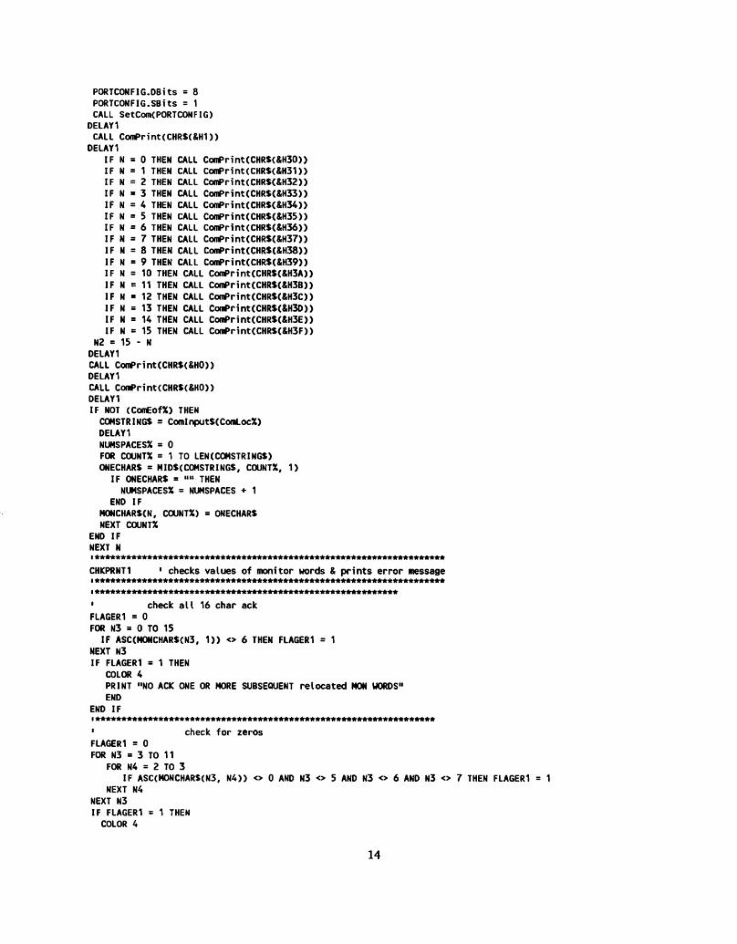
N = 0 N = 1 N = 2 N = 3 N = 4 N X 5 N X 6
PORTCONFIG.DBitS = 8 PORTCONFIG.SBits = 1 CALL SetCom(PORTCONFIG)
DELAY1 CALL ComPrint(CHR$(&H1))
DELAY1 THEN CALL ConiPrint(CHRS(&H30)) THEN CALL ComPrint(CHRS(&H31)) THEN CALL ComPrint(CHR$(&H32)) THEN CALL ComPrint(CHRS(&H33)) THEN CALL ComPrint(CHRS(&H34)) THEN CALL ComPrint(CHRS(&H35)) THEN CALL ComPrint(CHRS(&H36)) THEN CALL ComPrint(CHRS(&H37))
IF N = 8 THEN CALL ComPrint(CHRS(&H38)) IF N = 9 THEN CALL ComPrint(CHRS(&H39)) IF N = 10 THEN CALL ComPrint(CHRS(&H3A)) IF N = 11 THEN CALL ComPrint(CHRS(&H3B)) IF N = 12 THEN CALL ComPrint(CHRS(&H3C)) IF N = 13 THEN CALL ComPrint(CHRS(&H3D)) IF N = 14 THEN CALL ComPrint(CHRS(&H3E)) IF N = 15 THEN CALL ComPrint(CHRS(&H3F))
N2 = 15 - N DELAY1 CALL ComPrint(CHRS(&HO)) DELAY1 CALL CornPrint(CHRS(&HO)) DELAY1 IF NOT (ComEofX) THEN COMSTRINGS = ComlnputS(ComLocX) DELAY1 NUMSPACESX = 0 FOR COUNTX = 1 TO LEN(COMSTRINGS) ONECHARS = MIDS(COMSTRINGS, COUNTX, 1)
IF ONECHARS = "" THEN NUMSPACESX = NUMSPACES + 1
END IF MONCHARS(N, COUNTX) = ONECHARS NEXT COUNTX
END IF NEXT N i*******************************************************************
CHKPRNT1 ' checks values of monitor words & prints error message ******************************************************************** i**********************************************************
' check all 16 char ack FLAGER1 = 0 FOR N3 = 0 TO 15
IF ASC(HONCHAR$(N3, 1)) <> 6 THEN FLAGER1 = 1 NEXT N3 IF FLAGER1 = 1 THEN
COLOR 4 PRINT "NO ACK ONE OR MORE SUBSEQUENT relocated MON WORDS" END
END IF i*****************************************************************
' check for zeros FLAGER1 = 0 FOR N3 = 3 TO 11
FOR N4 = 2 TO 3 IF ASC(MONCHAR$(N3, N4)) <> 0 AND N3 <> 5 AND N3 <> 6 AND N3 <> 7 THEN FLAGER1 = 1
NEXT N4 NEXT N3 IF FLAGER1 = 1 THEN COLOR 4
14

PRINT "ONE OR MORE relocated MON WORDS NOT ZERO THAT SHOULD BE" END
END IF LOCATE 24, 1 PRINT "CHECKING ALL relocated 16 SIB MON WORDS 100 TIMES - CHECK #"; N5; NEXT N5 LOCATE 24, 1 PRINT " «; LOCATE 24, 1 COLOR 14 IF FLAGER3 = 1 THEN INPUT "SIB relocated 16 MON WORDS LOOK OK - PRESS ENTER TO CONTINUE"; TS IF FLAGER3 = 2 OR FLAGER3 = 3 THEN PRINT "SIB relocated 16 MON WORDS LOOK OK - PRESS ENTER TO CONTINUE"; TS
sssssssss
' send out digital control lines FOR N6 = 1 TO 12 ' types of STATE & CAL control conditions CLS IF FLAGER3 = 3 THEN N6 = 1 'initialize state for fe monit FELOOP: 'fe loop restart point for refresh display DO IF FLAGER3 = 3 THEN TS = INKEYS IF TS = "N" OR TS = "n" THEN LOCATE 23, 20 INPUT "PRESS ENTER TO CONTINUE"; TS N6 = N6 + 1 'increment cal condition for fe monit IF N6 > 3 THEN N6 = 1
END IF END IF IF FLAGER3 <> 3 THEN
IF N6 = 1 THEN XCH = &H3: CALCON = &H0 'CAL OFF & MOD OFF IF N6 = 2 THEN XCH = &H1: CALCON = &H1 'LO CAL MOD & MOD ON IF N6 = 3 THEN XCH = &H6: CALCON = &H1 'LO CAL MOO & MOD OFF IF N6 = 4 THEN XCH = &H4: CALCON = &H2 'LO CAL CONT & MOD ON IF N6 = 5 THEN XCH = &H3: CALCON = &H0 'CAL OFF & MOD OFF IF N6 = 6 THEN XCH = &H1: CALCON = &H4 'HI CAL MOO & MOO ON IF N6 = 7 THEN XCH = &H6: CALCON = &H4 'HI CAL MOD & MOD OFF IF N6 = 8 THEN XCH = &H4: CALCON = &H8 'HI CAL CONT & MOD OFF IF N6 = 9 THEN XCH = &H7: CALCON = &H0 'CAL OFF & MOD OFF IF N6 = 10 THEN XCH = &H5: CALCON = &H0 'CAL OFF & MOD OFF IF N6 = 11 THEN XCH = &H2: CALCON = &H2 'LO CAL CONT & MOD OFF IF N6 = 12 THEN XCH = &H0: CALCON = &H4 'HI CAL MOD & MOO OFF
END IF IF FLAGER3 = 3 THEN
IF N6 = 1 THEN XCH = &H7: CALCON = &H0 'COOL & CAL OFF & MOD OFF IF N6 = 2 THEN XCH = &H7: CALCON = &H2 'COOL & LO CAL MOD ON IF N6 = 3 THEN XCH = &H7: CALCON = &H8 'COOL & HI CAL MOD ON
END IF DELAY1 FOR DIGOUT = &H20 TO &H22 'dig out control adresses DELAY1 PORTCONFIG.Baud = 57600 PORTCONFIG.Parity = "E" PORTCONFIG.DBitS = 8 PORTCONFIG.SBits = 1 CALL SetCom(PORTCONFIG)
DELAY1 CALL ComPrint(CHRS(&H16)) DELAY1 PORTCONFIG.Baud = 57600 PORTCONFIG.Parity = "0" PORTCONFIG.DBitS = 8 PORTCONFIG.SBits = 1 CALL SetConKPORTCONFIG)
15

DELAY1 BNDADRHI = &H80 + BLKSTHI ' start adr + offset hi CALL ComPrint(CHR$(BNDADRHI)) • send adr hi
DELAY1 BNDADRLO = DI GOUT + BLKSTLO • start adr + offset lo CALL ComPrint(CHRS(BNDADRLO)) • send adr lo
DELAY1 IF DIGOUT = &H20 OR DIGOUT = &H21 THEN CALL ComPrint(CHR$(XCH)) • msb data out INCLDING &H21? ********** IF DIGOUT = &H22 THEN CALL ComPrint(CHRS(CALCON)) ' msb data out DELAY1 IF DIGOUT = &H20 OR DIGOUT = &H21 THEN CALL ComPrint(CHR$(XCH)) ' Isb data out INCLUDING &H21? ********** IF DIGOUT = &H22 THEN CALL ComPrint(CHRS(CALCON)) • msb data out DELAY1 IF NOT (ComEofX) THEN COMSTRINGS = ComlnputS(ComLocX) DELAY1 COLOR 3 NUMSPACESX = 0 FOR COUNTX = 1 TO LEN(COMSTRINGS) ONECHARS = MID$(COMSTRINGS, COUNTX, 1)
IF ONECHARS = "" THEN NUMSPACESX = NUMSPACES + 1
END IF NEXT COUNTX
END IF NEXT DIGOUT
' read all digital lines FOR DIGREAD = &H20 TO &H24 DELAY1 PORTCONFIG.Baud = 57600 PORTCONFIG.Parity = "E" PORTCONFIG.DBitS = 8 PORTCONFIG.SBits = 1 CALL SetCom(PORTCONFIG)
DELAY1 CALL ComPrint(CHRS(&Hl6))
DELAY1 PORTCONFIG.Baud = 57600 PORTCONFIG.Parity = "0" PORTCONFIG.DBitS = 8 PORTCONFIG.SBits = 1 CALL SetConKPORTCONFIG)
DELAY1 BNDADRHI = &H0 + BLKSTHI • start adr + offset hi CALL ComPrint(CHRS(BNDADRHI)) • send adr hi
DELAY1 BNDADRLO = DIGREAD + BLKSTLO • start adr + offset lo CALL ComPrint(CHRS(BNDADRLO)) ' send adr lo
DELAY1 CALL ComPrint(CHR$(&HO)) • msb filler
DELAY1 CALL ComPrint(CHRS(&HO)) • msb filler
DELAY1 IF NOT (ComEofX) THEN COMSTRINGS = ComlnputS(ComLocX)
DELAY1 COLOR 3 NUMSPACESX = 0 FOR COUNTX = 1 TO LEN(COMSTRINGS) ONECHARS = MID$(COMSTRINGS, COUNTX, 1)
IF ONECHARS = "" THEN NUMSPACESX = NUMSPACES + 1
END IF DIGCHAR$(DIGREAD, COUNTX, N6) = ONECHARS:
16
NEXT COUNTX END IF DELAY1 NEXT DIGREAD DELAY1 DELAY1 DELAY1 DELAY1 i**********************************************************************
' read all analog lines FOR ANLGRD = &H4 TO &H1F
FOR CNTX = 1 TO 3 FOR G6 = 1 TO 16
ANLGCHAR$(ANLGRD, CNTX, G6) = "0" NEXT G6
NEXT CNTX NEXT ANLGRD FOR ANLGRD = &H4 TO &H1F DELAY1 PORTCONFIG.Baud = 57600 PORTCONFIG.Parity = "E" PORTCONFIG.DBitS = 8 PORTCONFIG.SBits = 1 CALL SetCom(PORTCONFIG) CALL CofnPrint(CHRS(&Hl6))
DELAY1 PORTCONFIG.Baud - 57600 PORTCONFIG.Parity = "0" PORTCONFIG.DBitS = 8 PORTCONFIG.SBits = 1 CALL SetCom(PORTCONFIG)
DELAY1 BNDADRHI = &H0 + BLKSTHI ' start adr + offset hi CALL ComPrint(CHRS(BNDADRHI)) • send adr hi
DELAY1 BNDADRLO = ANLGRD + BLKSTLO • start adr + offset lo CALL ComPrint(CHRS(BNDADRLO)) • send adr lo
DELAY1 CALL ComPrint(CHRS(&HO)) • msb filler
DELAY1 CALL ComPrint(CHRS(&HO)) • Isb filler
DELAY1 IF NOT (ComEofX) THEN COMSTRINGS = ComlnputS(ComLocX)
DELAY1 COLOR 3 NUMSPACESX = 0 FOR COUNTX = 1 TO LEN(COMSTRINGS) ONECHARS = MIDS(COMSTRINGS, COUNTX, 1)
IF ONECHARS = "" THEN NUMSPACESX = NUMSPACES + 1
END IF ANLGCHAR$(ANLGRD, COUNTX, N6) = ONECHARS NEXT COUNTX
END IF DELAY1 NEXT ANLGRD i*********************************************************************
' check status of all returned data i*********************************************************************
1 print all data SCREEN 9 LINE (5, 5)-(295, 176), 14, B 'draw box LINE (7, 7)-(293, 174), 14, B 'draw box LINE (305, 5)-(600, 176), 14, B 'draw box
17
LINE (307, 7)-(598, 174), 14, B 'draw box COLOR 15 LOCATE 1, 3 PRINT " FE ELEC "; LOCATE 1, 25 PRINT " "; BANDS; » "; LOCATE 1, 41 PRINT " FE CRYO "; LOCATE 1, 63 PRINT " "; BANDS; " "; CALMODE = ASC(DIGCHARS(&H22, 3, N6))
IF CALMODE = 0 THEN CALS = "CAL OFF" = 1 THEN CALS = "LO CAL SW" = 2 THEN CALS = "LO CAL CONT" = 4 THEN CALS = "HI CAL SW" = 8 THEN CALS = "HI CAL CONT"
0 AND CALMODE <> 0 THEN SUMCHECK AND CALMODE <> 1 THEN SUMCHECK AND CALMODE <> 1 THEN SUMCHECK AND CALMODE <> 2 THEN SUMCHECK AND CALMODE <> 0 THEN SUMCHECK AND CALMODE <> 4 THEN SUMCHECK AND CALMODE <> 4 THEN SUMCHECK
IF CALMODE IF CALMODE IF CALMODE IF CALMODE THISCHK =
N6 = 1 / N6 = 2 i N6 = 3 i N6 = 4 i N6 = 5 i N6 = 6
IF N6 = 8 AND CALMODE <> 8 THEN SUMCHECK = IF N6 = 9 AND CALMODE <> 0 THEN SUMCHECK = IF N6 = 10 AND CALMODE <> 0 THEN SUMCHECK IF N6 = 11 AND CALMODE <> 2 THEN SUMCHECK IF N6 = 12 AND CALMODE <> 4 THEN SUMCHECK
6
SUMCHECK SUMCHECK SUMCHECK SUMCHECK SUMCHECK SUMCHECK SUMCHECK SUMCHECK SUMCHECK
= SUMCHECK + = SUMCHECK + = SUMCHECK +
THISCHK THISCHK THISCHK THISCHK THISCHK THISCHK THISCHK THISCHK THISCHK THISCHK = 1 THISCHK = 1 THISCHK = 1
LOCATE 3, COLOR 2 PRINT "CAL MODE"; LOCATE 3, 17 PRINT " »; LOCATE 3, 17 COLOR 13 IF THISCHK = 1 AND FLAGER3 <> 3 THEN COLOR 4: FLAGER3 = 1 PRINT CALS; IF FLAGER3 = 1
IF CMD IF IF IF IF IF IF
CMD = CMD = CMD •- CMD = CMD = CMD =
THISCHK IF N6 = IF N6 = IF N6 = IF N6 = IF N6 = IF N6 = IF N6 =
OR THEN THEN THEN
FLAGER3 = 2 THEN CMD = ASC(DIGCHAR$(&H20, 3, N6)) CMOS = "START" CMOS = "HEAT" CMOS = "STRESS"
THEN CMOS = "OFF" THEN CMOS = "PUMP" THEN CMOS = "COOL" OR CMD = 3 THEN CMOS = "INVALID"
0 AND CMD AND CMD AND CMD AND CMD AND CMD AND CMD AND CMD
IF N6 = 8 AND CMD IF N6 = 9 AND CMD
10 AND CMD 11 AND CMD 12 AND CMD
<> <> <> <> <> <> <> <> <> <> <> <>
IF N6 = 10 AND CMD <> 5 IF N6 = 11 AND CMD <> 2 IF N6 = 12 AND CMD <> 0
LOCATE 3, 41 COLOR 2 PRINT "CMD" LOCATE 3, 45 COLOR 13 IF THISCHK = 1 AND FLAGER3 <> 3
THEN SUMCHECK = THEN SUMCHECK = THEN SUMCHECK = THEN SUMCHECK = THEN SUMCHECK = THEN SUMCHECK = THEN SUMCHECK = THEN SUMCHECK = THEN SUMCHECK = THEN SUMCHECK THEN SUMCHECK THEN SUMCHECK
SUMCHECK SUMCHECK SUMCHECK SUMCHECK SUMCHECK SUMCHECK SUMCHECK SUMCHECK SUMCHECK
= SUMCHECK = SUMCHECK = SUMCHECK
THISCHK = THISCHK = THISCHK = THISCHK = THISCHK = THISCHK = THISCHK = THISCHK = THISCHK = THISCHK THISCHK
= 1 = 1
THISCHK = 1
THEN COLOR 4: FLAGER3 = 1
18

PRINT CMOS; SBIT3 = 0 SBIT4 = 0 SBIT5 = 0 State = ASC(DIGCHARS(&H21, 3, N6)) IF State >= 128 THEN State = State - 128 IF State >= 64 THEN State = State - 64 IF State >= 32 THEN State = State - 32 SBIT5 = 1
END IF IF State >= 16 THEN State = State - 16 SBIT4 = 1
END IF IF State >= 8 THEN State = State - 8 SBIT3 = 1
END IF IF State = IF State = IF State = IF State =
0 THEN STATEPS = "START" 2 THEN STATEPS = "HEAT" 4 THEN STATEPS = "STRESS" 5 THEN STATEPS = "OFF"
IF State = 6 THEN STATEPS = "PUMP" IF State = 7 THEN STATEPS = "COOL" IF State = 1 OR State = 3 THISCHK = 0 IF N6 = 1 AND State <> 3 IF N6 = 2 AND State <> 1 IF N6 = 3 AND State <> 6 IF N6 = 4 AND State <> 4 IF N6 ■ 5 AND State <> 3 IF N6 = 6 AND State <> 1 IF N6 = 7 AND State <> 6
8 AND State <> 4 9 AND State <> 7 10 AND State <> ! 11 AND State <> ', 12 AND State <> (
THEN STATEPS = "INVALID"
THEN SUMCHECK = THEN SUMCHECK = THEN SUMCHECK = THEN SUMCHECK = THEN SUMCHECK = THEN SUMCHECK = THEN SUMCHECK = THEN SUMCHECK = THEN SUMCHECK = THEN SUMCHECK = THEN SUMCHECK = THEN SUMCHECK =
SUMCHECK SUMCHECK SUMCHECK SUMCHECK SUMCHECK SUMCHECK SUMCHECK SUMCHECK SUMCHECK SUMCHECK + 1 SUMCHECK + 1 SUMCHECK + 1
IF N6 IF N6 IF N6 IF N6 IF N6
COLOR 2 LOCATE 3, 60 PRINT "STATE"; COLOR 13 IF THISCHK - 1 AND FLAGER3 <> 3 THEN COLOR 4: FLAGER3 = 1 LOCATE 3, 67 PRINT STATEPS; COLOR 2 LOCATE 14, 28 PRINT "COMPUT/MAN = "; COLOR 13 IF SBIT3 = 1 THEN PRINT "COMPUT"; IF SBIT3 = 0 THEN PRINT "MANUAL"; COLOR 2 LOCATE 5, 41 PRINT "PUMP REQ"; COLOR 13 LOCATE 5, 50 IF SBIT4 = 1 THEN PRINT "ON"; IF SBIT4 = 0 THEN PRINT "OFF"; COLOR 2 LOCATE 7, 41 PRINT "VALVE"; COLOR 13 LOCATE 7, 47 IF SBIT5 = 1 THEN PRINT "OPEN";
THISCHK = THISCHK = THISCHK = THISCHK = THISCHK = THISCHK = THISCHK = THISCHK = THISCHK = THISCHK = THISCHK = THISCHK =
19

IF SBIT5 = 0 THEN PRINT "CLOSED"; COLOR 2 LOCATE 5, 3 PRINT "CAL I"; PRINT " "; LOCATE 5, 8 COLOR 13 IF N6 < 4.5 OR N6 = 11 THEN NUM1& = ASC(ANLGCHARS(&H4, 2, N6)) NUM2& = ASC(ANLGCHARS(&H4, 3, N6)) AND &HF0 END IF IF N6 > 4.5 AND N6 <> 11 THEN NUM1& = ASC(ANLGCHARS(&H5, 2, N6)) NUM2& = ASC(ANLGCHARS(&H5, 3, N6)) AND &HF0 END IF SNUM = 0 IF NUM1& >= 128 THEN NUM1& = NUM1& - 128: SNUM = 1 ANVAL& = 256 * NUM1& + NUM2& IF SNUM = 1 THEN ANVAL& = 32768 - ANVAL& IF FLAGER3 = 3 THEN ANVAL = 1000 * ANVAL& / 32768 IF FLAGER3 < 3 THEN ANVAL = 1000 * ANVAL& / 32768 IF N6 < 4.5 OR N6 = 11 THEN ANVAL(&H4, N6) = ANVAL IF N6 > 4.5 AND N6 <> 11 THEN ANVAL(&H5, N6) = ANVAL THISCHK = 0
IF N6 = 1 AND (ANVAL < -500 OR ANVAL > IF N6 = 2 AND (ANVAL < -500 OR ANVAL > IF N6 = 3 AND (ANVAL < -500 OR ANVAL > IF N6 = 4 AND (ANVAL < -500 OR ANVAL > IF N6 = 5 AND (ANVAL < -500 OR ANVAL > IF N6 = 6 AND (ANVAL < -500 OR ANVAL > IF N6 = 7 AND (ANVAL < -500 OR ANVAL > IF N6 = 8 AND (ANVAL < -500 OR ANVAL > IF N6 = 9 AND (ANVAL < -500 OR ANVAL > IF N6 = 10 AND (ANVAL < -500 OR ANVAL > 500) THEN SUMCHECK = SUMCHECK + IF N6 = 11 AND (ANVAL < -500 OR ANVAL > 500) THEN SUMCHECK = SUMCHECK + IF N6 = 12 AND (ANVAL < -500 OR ANVAL > 500) THEN SUMCHECK = SUMCHECK + COLOR 13 IF THISCHK = 1 AND FLAGER3 <> 3 THEN COLOR 4: FLAGER3 = 1 PRINT INT(ANVAL);
COLOR 2 LOCATE 5, 15 PRINT "V"; LOCATE 5, 16 PRINT " "; LOCATE 5, 16 COLOR 13 IF N6 < 4.5 OR N6 = 11 THEN NUM1& = ASC(ANLGCHARS(&H6, 2, N6)) NUM2& = ASC(ANLGCHARS(&H6, 3, N6)) AND &HF0 END IF IF N6 > 4.5 AND N6 <> 11 THEN NUM1& = ASC(ANLGCHARS(&H7, 2, N6)) NUM2& = ASC(ANLGCHARS(&H7/ 3, N6)) AND &HF0 END IF SNUM = 0 IF NUM1& >= 128 THEN NUM1& = NUM1& - 128: SNUM = 1 ANVAL& = 256 * NUM1& + NUM2& IF SNUM = 1 THEN ANVAL& = 32768 - ANVAL& IF FLAGER3 = 3 THEN ANVAL = 4000 * ANVAL& / 32768 IF FLAGER3 < 3 THEN ANVAL = 4000 * ANVAL& / 32768 IF N6 < 4.5 OR N6 = 11 THEN ANVAL(&H6, N6) = ANVAL IF N6 > 4.5 AND N6 <> 11 THEN ANVAL(&H7, N6) = ANVAL THISCHK = 0
IF N6 = 1 AND (ANVAL < -25 OR ANVAL > 25) THEN SUMCHECK = SUMCHECK + 1: IF N6 = 2 AND (ANVAL < 2700 OR ANVAL > 2850) THEN SUMCHECK = SUMCHECK +
500) THEN SUMCHECK 500) THEN SUMCHECK 500) THEN SUMCHECK 500) THEN SUMCHECK 500) THEN SUMCHECK 500) THEN SUMCHECK 500) THEN SUMCHECK 500) THEN SUMCHECK 500) THEN SUMCHECK
SUMCHECK SUMCHECK SUMCHECK SUMCHECK SUMCHECK SUMCHECK SUMCHECK SUMCHECK SUMCHECK
THISCHK = THISCHK = THISCHK = THISCHK - THISCHK = THISCHK = THISCHK = THISCHK = THISCHK =
1: THISCHK = 1 1: THISCHK = 1 1: THISCHK = 1
THISCHK = 1 1: THISCHK = 1
20

IF N6 = 3 AND (ANVAL < -25 OR ANVAL > 25) THEN SUMCHECK = SUMCHECK + 1: THISCHK = 1 IF N6 = 4 AND (ANVAL < 2700 OR ANVAL > 2850) THEN SUMCHECK = SUMCHECK + 1: THISCHK = 1 IF N6 = 5 AND (ANVAL < -25 OR ANVAL > 25) THEN SUMCHECK = SUMCHECK + 1: THISCHK = 1 IF N6 = 6 AND (ANVAL < 2700 OR ANVAL > 2850) THEN SUMCHECK = SUMCHECK + 1: THISCHK = 1 IF N6 = 7 AND (ANVAL < -25 OR ANVAL > 25) THEN SUMCHECK = SUMCHECK + 1: THISCHK = 1 IF N6 = 8 AND (ANVAL < 2700 OR ANVAL > 2850) THEN SUMCHECK = SUMCHECK + 1: THISCHK = 1 IF N6 = 9 AND (ANVAL < -25 OR ANVAL > 25) THEN SUMCHECK = SUMCHECK + 1: THISCHK = 1 IF N6 = 10 AND (ANVAL < -25 OR ANVAL > 25) THEN SUMCHECK = SUMCHECK + 1: THISCHK = 1 IF N6 = 11 AND (ANVAL < 2700 OR ANVAL > 2850) THEN SUMCHECK = SUMCHECK + 1: THISCHK = 1 IF N6 = 12 AND (ANVAL < 2700 OR ANVAL > 2850) THEN SUMCHECK = SUMCHECK + 1: THISCHK = 1 COLOR 13 IF THISCHK = 1 AND FLAGER3 <> 3 THEN COLOR 4: FLAGER3 = 1 PRINT ANVAL / 100;
COLOR 2 LOCATE 5, 25 PRINT "LED"; LOCATE 5, 31 COLOR 13 NUM1& = ASC(ANLGCHARS(&HA, 2, N6)) NUM2& = ASC(ANLGCHARS(&HAr 3, N6)) AND &HF0 SNUM = 0 IF NUM1& >= 128 THEN NUM1& = NUM1& - 128: SNUM = 1 ANVAL& = 256 * NUM1& + NUM2& IF SNUM = 1 THEN ANVAL& = 32768 - ANVAL& IF FLAGER3 = 3 THEN ANVAL = 1000 * ANVAL& / 32768 IF FLAGER3 < 3 THEN ANVAL = 1000 * ANVAL& / 32768 ANVAL(&HA, N6) = ANVAL CHECKUM COLOR 13 PRINT ANVAL / 100; LOCATE 6, 25 COLOR 2 PRINT "SENS"; LOCATE 6, 31 COLOR 13 NUM1& = ASC(ANLGCHARS(&HB, 2, N6)) NUM2& = ASC(ANLGCHARS(&HB, 3, N6)) AND &HF0 SNUM = 0 IF NUM1& >= 128 THEN NUM1& = NUM1& - 128: SNUM = 1 ANVAL& = 256 * NUM1& + NUM2& IF SNUM = 1 THEN ANVAL& = 32768 - ANVAL&'- &H8000 IF FLAGER3 = 3 THEN ANVAL = 1000 * ANVAL& / 32768 IF FLAGER3 < 3 THEN ANVAL = 1000 * ANVAL& / 32768 ANVAL(&HB, N6) = ANVAL CHECKUM COLOR 13 PRINT ANVAL / 100; LOCATE 5, 60 COLOR 2 PRINT "AC I"; LOCATE 5, 65 COLOR 13 NUM1& = ASC(ANLGCHARS(&H9, 2, N6)) NUM2& = ASC(ANLGCHAR$(&H9, 3, N6)) AND &HF0 SNUM = 0 IF NUM1& >= 128 THEN NUM1& = NUM1& - 128: SNUM = 1 ANVAL& = 256 * NUM1& + NUM2& IF SNUM = 1 THEN ANVAL& = 32768 - ANVAL&'- &H8000 ANVAL = 1000 * ANVAL& / 32768 ANVAL(&H9, N6) = ANVAL CHECKUM COLOR 13 PRINT ANVAL / 100; LOCATE 7, 7 COLOR 2
21
PRINT "7.5v"; LOCATE 7, 12 COLOR 13 NUM1& = ASC(ANLGCHARS(&HC, 2, N6)) NUM2& = ASC(ANLGCHARS(&HC, 3, N6)) AND &HF0 SNUM = 0 IF NUM1& >= 128 THEN NUM1& = NUM1& - 128: SNUM = 1 ANVAL& = 256 * NUM1& + NUM2& IF SNUM = 1 THEN ANVAL& = 32768 - ANVAL&'- &H8000 IF FLAGER3 = 3 THEN ANVAL = 1000 * ANVAL& / 32768 IF FLAGER3 < 3 THEN ANVAL = 1000 * ANVAL& / 32768 ANVAL(&HC, N6) = ANVAL CHECKUM IF FLAGER3 < 3 THEN PRINT ANVAL / 100; IF FLAGER3 = 3 THEN COLOR 13 PRINT ANVAL / 1000;
END IF LOCATE 7, 23 COLOR 2 PRINT "GND"; LOCATE 7, 27 COLOR 13 NUM1& = ASC(ANLGCHARS(&HD, 2, N6)) NUM2& = ASC(ANLGCHARS(&HD, 3, N6)) AND &HF0 SNUM = 0 IF NUM1& >= 128 THEN NUM1& = NUM1& - 128: SNUM = 1 ANVAL& = 256 * NUM1& + NUM2& IF SNUM = 1 THEN ANVAL& = 32768 - ANVAL&'- &H8000 IF FLAGER3 = 3 THEN ANVAL = 1000 * ANVAL& / 32768 IF FLAGER3 < 3 THEN ANVAL = 1000 * ANVAL& / 32768 ANVAL(&HD, N6) = ANVAL THISCHK = 0
IF N6 = 1 AND (ANVAL < -25 OR ANVAL > 25) THEN SUMCHECK = SUMCHECK + 1: THISCHK = IF N6 = 2 AND (ANVAL < -25 OR ANVAL > 25) THEN SUMCHECK = SUMCHECK + 1: THISCHK = IF N6 = 3 AND (ANVAL < -25 OR ANVAL > 25) THEN SUMCHECK = SUMCHECK + 1: THISCHK = IF N6 = 4 AND (ANVAL < -25 OR ANVAL > 25) THEN SUMCHECK = SUMCHECK + 1: THISCHK = IF N6 = 5 AND (ANVAL < -25 OR ANVAL > 25) THEN SUMCHECK = SUMCHECK + 1: THISCHK = IF N6 = 6 AND (ANVAL < -25 OR ANVAL > 25) THEN SUMCHECK = SUMCHECK + 1: THISCHK = IF N6 = 7 AND (ANVAL < -25 OR ANVAL > 25) THEN SUMCHECK = SUMCHECK + 1: THISCHK = IF N6 = 8 AND (ANVAL < -25 OR ANVAL > 25) THEN SUMCHECK = SUMCHECK + 1: THISCHK = IF N6 = 9 AND (ANVAL < -25 OR ANVAL > 25) THEN SUMCHECK = SUMCHECK + 1: THISCHK = IF N6 = 10 AND (ANVAL < -25 OR ANVAL > 25) THEN SUMCHECK = SUMCHECK + 1: THISCHK = 1 IF N6 = 11 AND (ANVAL < -25 OR ANVAL > 25) THEN SUMCHECK = SUMCHECK + 1: THISCHK = 1 IF N6 = 12 AND (ANVAL < -25 OR ANVAL > 25) THEN SUMCHECK = SUMCHECK + 1: THISCHK = 1
COLOR 13 IF THISCHK = 1 AND FLAGER3 <> 3 THEN COLOR 4: FLAGER3 = 1 IF FLAGER3 < 3 THEN PRINT ANVAL / 100; IF FLAGER3 = 3 THEN
COLOR 13 PRINT ANVAL / 1000;
END IF LOCATE 7, 60 COLOR 2 PRINT "15K" LOCATE 7, 64 COLOR 13 NUM1& = ASC(ANLGCHARS(&H14, 2, N6)) NUM2& = ASC(ANLGCHARS(&H14, 3, N6)) AND &HF0 SNUM = 0 IF NUM1& >= 128 THEN NUM1& = NUM1& - 128: SNUM = 1 ANVAL& = 256 * NUM1& + NUM2& IF SNUM = 1 THEN ANVAL& = 32768 - ANVALfc'- &H8000 IF FLAGER3 = 3 THEN ANVAL = 1000 * ANVAL& / 32768 IF FLAGER3 < 3 THEN ANVAL = 1000 * ANVAL& / 32768
22
ANVAL(&H14, N6) = ANVAL CHECKUM IF FLAGER3 < 3 THEN PRINT ANVAL / 100; IF FLAGER3 = 3 THEN
COLOR 13 PRINT ANVAL;
END IF LOCATE 9, 3 COLOR 2 PRINT "LF FET #1"; LOCATE 9, 13 COLOR 13 NUM1& = ASC(ANLGCHARS(&H10, 2, N6)) NUM2& = ASC(ANLGCHARS(&H10( 3, N6)) AND &HF0 SNUM = 0 IF NUM1& >= 128 THEN NUM1& = NUM1& - 128: SNUM = 1 ANVAL& = 256 * NUM1& + NUM2& IF SNUM = 1 THEN ANVAL& = 32768 - ANVALft'- &H8000 IF FLAGER3 = 3 THEN ANVAL = 1000 * ANVAL& / 32768 IF FLAGER3 < 3 THEN ANVAL = 1000 * ANVAL& / 32768 ANVAL(&H10, N6) = ANVAL CHECKUM IF FLAGER3 < 3 THEN PRINT ANVAL / 100; IF FLAGER3 = 3 THEN
COLOR 13 PRINT ANVAL / 100;
END IF LOCATE 9, 22 COLOR 2 PRINT "RT FET #1" LOCATE 9, 32 COLOR 13 NUM1& = ASC(ANLGCHARS(&H11, 2, N6)) NUM2& = ASC(ANLGCHARS(&H11, 3, N6)) AND &HF0 SNUM = 0 IF NUM1& >= 128 THEN NUM1& = NUM1& - 128: SNUM = 1 ANVAL& = 256 * NUM1& + NUM2& IF SNUM = 1 THEN ANVAL& = 32768 - ANVAL&'- &H8000 IF FLAGER3 = 3 THEN ANVAL = 1000 * ANVAL& / 32768 IF FLAGER3 < 3 THEN ANVAL = 1000 * ANVAL& / 32768 ANVAL(&H11, N6) = ANVAL CHECKUM IF FLAGER3 < 3 THEN PRINT ANVAL / 100; IF FLAGER3 = 3 THEN
COLOR 13 PRINT ANVAL / 100;
END IF LOCATE 9, 41 COLOR 2 PRINT "PUMP VAC"; LOCATE 9, 50 COLOR 13 NUM1& = ASC(ANLGCHARS(&H8, 2, N6)) NUM2& = ASC(ANLGCHARS(&H8, 3, N6)) AND &HF0 SNUM = 0 IF NUM1& >= 128 THEN NUM1& = NUM1& - 128: SNUM = 1 ANVAL& = 256 * NUM1& + NUM2& IF SNUM = 1 THEN ANVAL& = 32768 - ANVAL&'- &H8000 IF FLAGER3 = 3 THEN ANVAL = 1000 * ANVAL& / 32768 IF FLAGER3 < 3 THEN ANVAL = 1000 * ANVAL& / 32768 ANVAL(&H8, N6) = ANVAL CHECKUM IF FLAGER3 < 3 THEN PRINT ANVAL / 100;
23

PRINT ANVAL; END IF LOCATE 9, 60 COLOR 2 PRINT "50K"; LOCATE 9, 64 COLOR 13 NUM1& = ASC(ANLGCHARS(&H15, 2, N6)) NUM2& = ASC(ANLGCHARS(&H15, 3, N6)) AND &HF0 SNUM = 0 IF NUM1& >= 128 THEN NUM1& = NUM1& - 128: SNUM = 1 ANVAL& = 256 * NUM1& + NUM2& IF SNUM = 1 THEN ANVAL& = 32768 - ANVAL&'- &H8000 IF FLAGER3 = 3 THEN ANVAL = 1000 * ANVAL& / 32768 IF FLAGER3 < 3 THEN ANVAL - 1000 * ANVAL& / 32768 ANVAL(&H15, N6) = ANVAL CHECKUM IF FLAGER3 < 3 THEN PRINT ANVAL / 100; IF FLAGER3 = 3 THEN
COLOR 13 PRINT ANVAL;
END IF LOCATE 11, 3 COLOR 2 PRINT "LF FET #2"; LOCATE 11, 13 COLOR 13 NUM1& = ASC(ANLGCHAR$(&H12, 2, N6)) NUM2& = ASC(ANLGCHARS(&H12, 3, N6)) AND &HF0 SNUM = 0 IF NUM1& >= 128 THEN NUM1& = NUM1& - 128: SNUM = 1 ANVAL& = 256 * NUM1& + NUM2& IF SNUM = 1 THEN ANVAL& = 32768 - ANVAL&'- &H8000 IF FLAGER3 = 3 THEN ANVAL = 1000 * ANVAL& / 32768 IF FLAGER3 < 3 THEN ANVAL = 1000 * ANVAL& / 32768 ANVAL(&H12, N6) = ANVAL CHECKUM IF FLAGER3 < 3 THEN PRINT ANVAL / 100; IF FLAGER3 = 3 THEN
COLOR 13 PRINT ANVAL / 100;
END IF LOCATE 11, 22 COLOR 2 PRINT "RT FET #2"; LOCATE 11, 32 COLOR 13 NUM1& = ASC(ANLGCHARS(&H13, 2, N6)) NUM2& - ASC(ANLGCHARS(&H13, 3, N6)) AND &HF0 SNUM = 0 IF NUM1& >= 128 THEN NUM1& - NUM1& - 128: SNUM = 1 ANVAL& = 256 * NUM1& + NUM2& IF SNUM = 1 THEN ANVAL& = 32768 - ANVAL&'- &H8000 IF FLAGER3 = 3 THEN ANVAL = 1000 * ANVAL& / 32768 IF FLAGER3 < 3 THEN ANVAL = 1000 * ANVAL& / 32768 ANVAL(&H13, N6) = ANVAL CHECKUM IF FLAGER3 < 3 THEN PRINT ANVAL / 100; IF FLAGER3 = 3 THEN
COLOR 13 PRINT ANVAL / 100;
END IF LOCATE 11, 41 COLOR 2 PRINT "DEWER VAC";
24

LOCATE 11, 51 COLOR 13 NUM1& = ASC(ANLGCHAR$(&H17, 2, N6)) NUM2& = ASC(ANLGCHARS(&H17, 3, N6)) AND &HF0 SNUM = 0 IF NUM1& >= 128 THEN NUM1& = NUM1& - 128: SNUM = 1 ANVAL& = 256 * NUM1& + NUM2& IF SNUM = 1 THEN ANVAL& = 32768 - ANVAL&'- &H8000 IF FLAGER3 = 3 THEN ANVAL = 1000 * ANVAL& / 32768 IF FLAGER3 < 3 THEN ANVAL = 1000 * ANVAL& / 32768 ANVAL(&H17, N6) = ANVAL CHECKUM IF FLAGER3 < 3 THEN PRINT ANVAL / 100; IF FLAGER3 = 3 THEN
COLOR 13 PRINT ANVAL;
END IF LOCATE 11, 60 COLOR 2 PRINT "SOOK"; LOCATE 11, 65 COLOR 13 NUM1& = ASC(ANLGCHARS(&H16, 2, N6)) NUN2& = ASC(ANLGCHARS(&H16, 3, N6)) AND &HF0 SNUM = 0 IF NUM1& >= 128 THEN NUM1& = NUM1& - 128: SNUM = 1 ANVAL& = 256 * NUM1& + NUM2& IF SNUM = 1 THEN ANVAL& = 32768 - ANVAL&'- &H8000 IF FLAGER3 = 3 THEN ANVAL = 1000 * ANVAL& / 32768 IF FLAGER3 < 3 THEN ANVAL = 1000 * ANVAL& / 32768 ANVAL(&H16, N6) = ANVAL CHECKUM IF FLAGER3 = 3 THEN COLOR 13 PRINT ANVAL;
END IF IF FLAGER3 < 3 THEN PRINT ANVAL / 100; FULIDS = HEX$(ASC(DIGCHARS(&H23, 2, 1))) + HEX$(ASC(DIGCHARS(&H23, 3, 1))) FREQS = RIGHTS(FULIDS, 1) MMOD1S = MID$(FULIDS, 3, 1) MMOD = ASC(MMODIS) IF MMOD >= 48 AND MMOD <= 57 THEN MMOD = MMOD - 48 IF MMOD >= 65 AND MMOD <= 70 THEN MMOD = MMOD - 55 IF MMOD >= 8 THEN MMOO = MMOD - 8 IF MMOD >= 4 THEN MMOD = MMOD - 4 HISNS = MIDS(FULIDS, 1,1) HISN = ASC(HISNS) IF HISN >= 48 AND HISN <= 57 THEN HISN = HISN - 48 IF HISN >= 65 AND HISN <= 70 THEN HISN = HISN - 55 SNSUM = 0 IF HISN >= 8 THEN HISN = HISN - 8 IF HISN >= 4 THEN HISN = HISN - 4 IF HISN >= 2 THEN HISN = HISN - 2: SNSUM = SNSUM + 32 IF HISN >= 1 THEN HISN = HISN - 1: SNSUM = SNSUM + 16 LOSNS = MID$(FULID$, 2, 1) LOSN = ASC(LOSNS) IF LOSN >= 48 AND LOSN <= 57 THEN LOSN = LOSN - 48 IF LOSN >= 65 AND LOSN <= 70 THEN LOSN = LOSN - 55 IF LOSN >= 8 THEN LOSN = LOSN - 8: SNSUM = SNSUM + 8 IF LOSN >= 4 THEN LOSN = LOSN - 4: SNSUM = SNSUM + 4 IF LOSN >= 2 THEN LOSN = LOSN - 2: SNSUM = SNSUM + 2 IF LOSN >= 1 THEN LOSN = LOSN - 1: SNSUM = SNSUM + 1
NUM1& = ASC(ANLGCHAR$(&H18, 2, N6))
25

NUM2& = ASC(ANLGCHARS(&H18, 3, N6)) AND &HFO SNUM = 0 IF NUM1& >= 128 THEN NUM1& = NUM1& - 128: SNUM = 1 ANVAL& = 256 * NUM1& + NUM2& IF SNUM = 1 THEN ANVAL& = 32768 - ANVAL& ANVAL = 1000 * ANVAL& / 32768 ANVAL(&H18, N6) = ANVAL CHAN(1) = ANVAL NUM1& = ASC(ANLGCHARS(&H19, 2, N6)) NUM2& = ASC(ANLGCHARS(&H19, 3, N6)) AND &HF0 SNUM = 0 IF NUM1& >= 128 THEN NUM1& = NUM1& - 128: SNUM = 1 ANVAL& = 256 * NUM1& + NUM2& IF SNUM = 1 THEN ANVAL& = 32768 - ANVAL& ANVAL = 1000 * ANVAL& / 32768 ANVAL(&H19, N6) = ANVAL CHAN(2) = ANVAL NUM1& = ASC(ANLGCHARS(&H1A, 2, N6)) NUM2& = ASC(ANLGCHARS(&H1A, 3, N6)) AND &HF0 SNUM = 0 IF NUM1& >= 128 THEN NUM1& = NUM1& - 128: SNUM = 1 ANVAL& = 256 * NUM1& + NUM2& IF SNUM = 1 THEN ANVAL& = 32768 - ANVAL& ANVAL = 1000 * ANVAL& / 32768 ANVAL(&H1A, N6) = ANVAL CHAN(3) = ANVAL NUM1& = ASC(ANLGCHARS(&H1B, 2, N6)) NUM2& = ASC(ANLGCHARS(&H1B, 3, N6)) AND &HF0 SNUM = 0 IF NUM1& >= 128 THEN NUM1& = NUM1& - 128: SNUM = 1 ANVAL& = 256 * NUM1& + NUM2& IF SNUM = 1 THEN ANVAL& = 32768 - ANVAL& ANVAL = 1000 * ANVAL& / 32768 ANVAL(&H1B, N6) = ANVAL CHAN(4) = ANVAL NUM1& = ASC(ANLGCHARS(&H1C, 2, N6)) NUM2& = ASC(ANLGCHARS(&H1C, 3, N6)) AND &HF0 SNUM = 0 IF NUM1& >= 128 THEN NUM1& = NUM1& - 128: SNUM = 1 ANVAL& = 256 * NUM1& + NUM2& IF SNUM = 1 THEN ANVAL& = 32768 - ANVAL& ANVAL = 1000 * ANVAL& / 32768 ANVAL(&H1C, N6) = ANVAL CHAN(5) = ANVAL NUM1& = ASC(ANLGCHARS(&H1D, 2, N6)) NUM2& = ASC(ANLGCHARS(&H1D, 3, N6)) AND &HF0 SNUM = 0 IF NUM1& >= 128 THEN NUM1& = NUM1& - 128: SNUM = 1 ANVAL& = 256 * NUM1& + NUM2& IF SNUM = 1 THEN ANVAL& = 32768 - ANVAL& ANVAL = 1000 * ANVAL& / 32768 ANVAL(&H1D, N6) = ANVAL CHAN(6) = ANVAL NUM1& = ASC(ANLGCHARS(&H1E, 2, N6)) NUM2& = ASC(ANLGCHARS(&H1E, 3, N6)) AND &HF0 SNUM = 0 IF NUM1& >= 128 THEN NUM1& = NUM1& - 128: SNUM = 1 ANVAL& = 256 * NUM1& + NUM2& IF SNUM = 1 THEN ANVAL& = 32768 - ANVAL& ANVAL = 1000 * ANVAL& / 32768 ANVAL(&H1E, N6) = ANVAL CHAN(7) = ANVAL NUM1& = ASC(ANLGCHAR$(&H1F, 2, N6)) NUM2& = ASC(ANLGCHAR$(&H1F, 3, N6)) AND &HF0 SNUM = 0
26
IF NUM1& >= 128 THEN NUM1& = NUM1& - 128: SNUM = 1 ANVAL& = 256 * NUM1& + NUM2& IF SNUM = 1 THEN ANVAL& = 32768 - ANVAL& ANVAL = 1000 * ANVAL& / 32768 ANVAL(&H1F, N6) = ANVAL CHAN(8) = ANVAL FOR N = 1 TO 8 ANVAL = CHAN(N) CHECKUM
IF THISCHK > 0 THEN COLOR 4 PRINT "BAD AUX ANLALOG"
END IF IF THISCHK = 0 THEN COLOR 13
NEXT N i*****************************************************************
' test faces IF FLAGER3 = 1 OR FLAGER3 = 2 THEN LOCATE 15, 1 IF SUMCHECK < .5 THEN COLOR 2
ADR"
20 & 22";
*II
* *II.
READ-BACK";
* *II
* *II.
DIGITAL COMMANDS";
* *II
* *II.
OK";
* *II
.5 THEN
ADR"
20 & 22";
READ-BACK";
DIGITAL COMMANDS";
PRINT II
COLOR 3 PRINT H *l COLOR 2 PRINT II
COLOR 3 PRINT II
PRINT II <
COLOR 2 PRINT II
COLOR 3 PRINT II
PRINT II
COLOR 2 PRINT n COLOR 3 PRINT II
PRINT II
COLOR 13 PRINT •i
COLOR 3 PRINT u LOCATE 21, 1
END IF IF SUMCHECK > COLOR 2 PRINT H COLOR 4 PRINT mi. f COLOR 2 PRINT H COLOR 4 PRINT Mil
PRINT llll. 1
COLOR 2 PRINT n
COLOR 4 PRINT llll
PRINT llll. f
COLOR 2 PRINT n
COLOR 4 PRINT llll
27
COLOR 13 PRINT " OK"; COLOR 4 LOCATE 21, 1
END IF END IF i*****************************************************************
IF ((FLAGER3 = 1 OR FLAGER3 = 2) AND SUMCHECK < .5) OR FLAGER3 = 3 THEN LOCATE 20, 11 COLOR 3 PRINT " ********** *II
PRINT » *"; COLOR 2 PRINT " F117 SN = "; COLOR 13 PRINT ASC(DIGCHARS(&H24, 3, 1)); COLOR 2 PRINT " ID = "; COLOR 13 PRINT IDN; COLOR 2 PRINT " BAND = "; COLOR 13 PRINT BANDS; COLOR 3 PRINT " *" PRINT " *"; COLOR 2 PRINT " FE SN = "; COLOR 13 PRINT SNSUM; COLOR 2 PRINT " FE FREQ = »; COLOR 13 PRINT FREQS; COLOR 2 PRINT " MOD = "; COLOR 13 PRINT MMOD; COLOR 3 PRINT " *" PRINT " *"; COLOR 14 IF FLAGER3 <> 3 THEN PRINT " PRESS ENTER TO CONTINUE"; END IF IF FLAGER3 = 3 THEN PRINT " "; END IF COLOR 3 PRINT " *" PRINT " ********** *II.
END IF IF (FLAGER3 = 1 OR FLAGER3 = 2) AND SUMCHECK > .5 THEN LOCATE 20, 1 COLOR 4 PRINT " ************** *ii
PRINT " *"; COLOR 2 PRINT " F117 SN = "; COLOR 13 PRINT ASC(DIGCHARS(&H24, 3, 1)); COLOR 2 PRINT " ID = "; COLOR 13
28
PRINT IDN; COLOR 2 PRINT " BAND = "; COLOR 13 PRINT BANDS; COLOR 4 PRINT " *" PRINT " *"; COLOR 2 PRINT " FE SN = "; COLOR 13 PRINT SNSUM; COLOR 2 PRINT " FE FREQ = "; COLOR 13 PRINT FREQS; COLOR 2 PRINT " MOD = •'; COLOR 13 PRINT MMOD; COLOR 4 PRINT " *" PRINT " *"; COLOR 14 IF FLAGER3 <> 3 THEN PRINT " PRESS ENTER TO CONTINUE"; END IF IF FLAGER3 = 3 THEN PRINT " "; END IF COLOR 4 PRINT " *" PRINT" ****************
END IF LOCATE 23, 26
PRINT " "; COLOR 14 IF FLAGER3 = 1 THEN LOCATE 23, 26 INPUT "PRESS ENTER TO CONTINUE"; TS
END IF IF FLAGER3 = 3 THEN LOCATE 23, 20 PRINT " "; LOCATE 23, 14 PRINT "PRESS "; COLOR 13 PRINT "C"; COLOR 3 PRINT " FOR CRYO "; COLOR 13 PRINT " N"; COLOR 3 PRINT " FOR NEXT CAL OR "; COLOR 13 PRINT "Q"; COLOR 3 PRINT " TO QUIT"; T3S = INKEYS LOCATE 15, 20 PRINT "7 FOR COOL" LOCATE 16, 20 PRINT "4 FOR STRESS" LOCATE 17, 20 PRINT "5 FOR OFF"
29
LOCATE 15, 45 PRINT "2 FOR HEAT" LOCATE 16, 45 PRINT "6 FOR PUMP" LOCATE 17, 45 PRINT "0 FOR STARTUP" LOCATE 18, 28 COLOR 2 IF TS = "C" OR TS = "c" THEN
INPUT "ENTER CRYO CMD # ="; CMD END IF
END IF IF FLAGER3 = 2 OR FLAGER3 = 3 THEN TS = "" IF FLAGER3 = 3 AND T3$ <> "Q" AND T3S <> "q" THEN GOTO FELOOP LOOP UNTIL TS = "" LOCATE 25, 28 PRINT " " LOCATE 25, 28
IF IF IF IF IF IF IF IF IF IF IF IF IF IF IF IF IF IF IF IF IF IF IF IF
COLOR PRINT COLOR PRINT COLOR
AND N9 = &H4 THEN N9S AND N9 = &H5 THEN N9S AND N9 = &H6 THEN N9S
' backup display IF FLAGER3 = 1 OR FLAGER3 = 3 THEN CLS FOR N9 = &H4 TO &H1F COEF! = 1 DIV! = 100 IF FLAGER3 <> 2
FLAGER3 <> 2 FLAGER3 <> 2 FLAGER3 <> 2 FLAGER3 <> 2 FLAGER3 <> 2 FLAGER3 <> 2 FLAGER3 <> 2 FLAGER3 <> 2 FLAGER3 <> 2 FLAGER3 <> 2 FLAGER3 <> 2 FLAGER3 <> 2 FLAGER3 <> 2 FLAGER3 <> 2 FLAGER3 <> 2 FLAGER3 <> 2 FLAGER3 <> 2 FLAGER3 <> 2 FLAGER3 <> 2 FLAGER3 <> 2 FLAGER3 <> 2 FLAGER3 <> 2 FLAGER3 <> 2 FLAGER3 <> 2
COLOR 3 LOCATE 1, 1 PRINT "TEST STATE
13 N6; 2 " ANALOG = 13
'display for man test
= "ma": XI =
AND N9 AND N9 AND N9 AND N9 AND N9 AND N9 AND N9 AND N9 AND N9 AND N9 AND N9 AND N9
AND N9 AND N9 AND N9 AND N9 AND N9 AND N9 AND N9 AND N9
&H7 THEN N9S = &H8 THEN N9S = &H9 THEN N9S = &HA THEN N9S = &HB THEN N9S = &HC THEN N9S = &HD THEN N9$ = &H10 THEN N9S &H11 THEN N9S &H12 THEN N9S &H13 THEN N9S &H14 THEN N9S
AND N9 = &H15 THEN N9S AND N9 = &H16 THEN N9S
&H17 THEN N9$ &H18 THEN N9S &H19 THEN N9S &H1A THEN N9S &H1B THEN N9$ &H1C THEN N9S &H1D THEN N9S &H1E THEN N9S
"ma" "V": "V": "V": "A": "V": "V": "V": "V":
• nyii : 'lyi - iiyn
= "V" - iigii - IIKII
= "K" - iiyu
s iiV" - iiyu - iiyu - iiyu - iiyu - iiyu - iiyu
XI = XI = XI = XI = XI = XI = XI = XI = XI = XI XI XI XI XI XI XI XI XI XI XI XI XI X1 XI
Yl = 3 Yl = 4
Y1 Yl Yl Yl Yl Yl Yl Yl
25: 25: 25: 25: 25: 25: 25: 25: 50: 50: 50: 50: 50: 50: 50:
5' 6 7 8 9 10 11 12 3 4 5 6 7 8 9 10 4 5 6 7 8 9 10
IF N6 = 1 OR N6 = 2 OR N6 = 5 OR N6 = 6 OR N6 = 11 OR N6 = 12 THEN PRINT "8.2"; OR N6 = 4 OR N6 = 7 OR N6 = 8 OR N6 = 9 OR N6 = 10 THEN PRINT "0"; IF N6
COLOR PRINT COLOR
MOD =
= 3 2 n v
13 IF N6 = 1 OR N6 IF N6 = 3 OR N6
2 OR N6 = 5 OR N6 = 6 OR N6 = 8 OR N6 = 11 OR N6 = 12 THEN PRINT "ON/0"; 4 OR N6 = 7 OR N6 = 8 OR N6 = 9 OR N6 = 10 THEN PRINT "OFF/I";
30

COLOR 2 PRINT " EVEN BITS = "; COLOR 13 IF N6 = 1 OR N6 = 2 OR N6 = 5 OR N6 = 6 OR N6 IF N6 = 3 OR N6 = 4 OR N6 = 7 OR N6 = 8 OR N6 COLOR 2 PRINT " ODD BITS = "; COLOR 13 IF N6 = 1 OR N6 = 3 OR N6 = 5 OR N6 = 7 OR N6
9 OR N6 = 10 THEN PRINT "0"; 11 OR N6 = 12 THEN PRINT "1";
9 OR N6 = 11 THEN PRINT "0"; 10 OR N6 = 12 THEN PRINT "1";
COLOR 2 LOCATE Yl, XI IF N9 <> &HE AND N9 <> &HF THEN PRINT "ADR "; HEX$(N9); « «; COLOR 13 IF N9 <> &HE AND N9 <> &HF THEN PRINT (COEF! * ANVAL(N9, N6)) / DIV!; N9$ COLOR 2 LOCATE 14, 1 PRINT "CMD MONIT WORD &H20 ="; COLOR 13 CHAR1 = ASC(DIGCHARS(&H20, 3, N6)) PRINT CHAR1; IF CHAR1 < 128 THEN BITC8 = 0 IF CHAR1 >= 128 THEN BITC8 = 1 CHAR1 = CHAR1 - 128
END IF IF CHAR1 < 64 THEN BITC7 = 0 IF CHAR1 >= 64 THEN BITC7 = 1 CHAR1 = CHAR1 - 64
END IF IF CHAR1 < 32 THEN BITC6 = 0 IF CHAR1 >= 32 THEN BITC6 = 1 CHAR1 = CHAR1 - 32
END IF IF CHAR1 < 16 THEN BITC5 = 0 IF CHAR1 >= 16 THEN BITC5 = 1 CHAR1 = CHAR1 - 16
END IF IF CHAR1 < 8 THEN BITC4 = 0 IF CHAR1 >= 8 THEN BITC4 = 1 CHAR1 = CHAR1 - 8
END IF IF CHAR1 < 4 THEN BITC3 = 0 IF CHAR1 >= 4 THEN BITC3 = 1 CHAR1 = CHAR1 - 4
END IF IF CHAR1 < 2 THEN BITC2 = 0 IF CHAR1 >= 2 THEN BITC2 = 1 CHAR1 = CHAR1 - 2
END IF BITC1 = CHAR1
LOCATE 14, 30
PRINT " "; BITC8; BITC7; BITC6; BITC5; BITC4; BITC3; BITC2; BITC1 COLOR 2 PRINT "CAL MONIT WORD &H21 ="; COLOR 13 CHAR1 = ASC(DIGCHAR$(&H21, 3, N6)) PRINT CHAR1;
31
IF CHAR1 < 128 THEN BITC8 = 0 IF CHAR1 >= 128 THEN BITC8 = 1 CHAR1 = CHAR1 - 128
END IF IF CHAR1 < 64 THEN BITC7 = 0 IF CHAR1 >= 64 THEN BITC7 = 1 CHAR1 = CHAR1 - 64
END IF IF CHAR1 < 32 THEN BITC6 = 0 IF CHAR1 >= 32 THEN BITC6 = 1 CHAR1 = CHAR1 - 32
END IF IF CHAR1 < 16 THEN BITC5 = 0 IF CHAR1 >= 16 THEN BITC5 = 1 CHAR1 - CHAR1 - 16
END IF IF CHAR1 < 8 THEN BITC4 = 0 IF CHAR1 >= 8 THEN BITC4 = 1 CHAR1 = CHAR1 - 8
END IF IF CHAR1 < 4 THEN BITC3 = 0 IF CHAR1 >= 4 THEN BITC3 = 1 CHAR1 = CHAR1 • 4
END IF IF CHAR1 < 2 THEN BITC2 = 0 IF CHAR1 >= 2 THEN BITC2 = 1 CHAR1 = CHAR1 - 2
END IF BITC1 = CHAR1
LOCATE 15, 30 PRINT " "; BITC8; BITC7; BITC6; BITC5; BITC4; BITC3; BITC2; BITC1 COLOR 2 PRINT "STATE MONIT WORD &H22 ="; COLOR 13 CHAR1 = ASC(DIGCHARS(&H22, 3, N6)) PRINT CHAR1; IF CHAR1 < 128 THEN BITC8 = 0 IF CHAR1 >= 128 THEN BITC8 = 1 CHAR1 = CHAR1 - 128
END IF IF CHAR1 < 64 THEN BITC7 = 0 IF CHAR1 >= 64 THEN BITC7 = 1 CHAR1 = CHAR1 - 64
END IF IF CHAR1 < 32 THEN BITC6 = 0 IF CHAR1 >= 32 THEN BITC6 = 1 CHAR1 = CHAR1 - 32
END IF IF CHAR1 < 16 THEN BITC5 = 0 IF CHAR1 >= 16 THEN BITC5 = 1 CHAR1 = CHAR1 - 16
END IF IF CHAR1 < 8 THEN BITC4 = 0 IF CHAR1 >= 8 THEN
32
BITC4 = 1 CHAR1 = CHAR1 - 8
END IF IF CHAR1 < 4 THEN BITC3 = 0 IF CHAR1 >= 4 THEN BITC3 = 1 CHAR1 = CHAR1 - 4
END IF IF CHAR1 < 2 THEN BITC2 = 0 IF CHAR1 >= 2 THEN BITC2 = 1 CHAR1 = CHAR1 - 2
END IF BITC1 = CHAR1
LOCATE 16, 30 PRINT " "; BITC8; BITC7; BITC6; BITC5; BITC4; BITC3; BITC2; BITC1 COLOR 2 PRINT "ID1 MONIT WORD &H23 ="; COLOR 13 CHAR1 = ASC(DIGCHARS(&H23, 2, N6)) PRINT CHAR1; IF CHAR1 < 128 THEN BITC8 = 0 IF CHAR1 >= 128 THEN BITC8 = 1 CHAR1 = CHAR1 - 128
END IF IF CHAR1 < 64 THEN BITC7 = 0 IF CHAR1 >= 64 THEN BITC7 = 1 CHAR1 = CHAR1 - 64
END IF IF CHAR1 < 32 THEN BITC6 = 0 IF CHAR1 >= 32 THEN BITC6 = 1 CHAR1 = CHAR1 - 32
END IF IF CHAR1 < 16 THEN BITC5 = 0 IF CHAR1 >= 16 THEN BITC5 = 1 CHAR1 = CHAR1 - 16
END IF IF CHAR1 < 8 THEN BITC4 = 0 IF CHAR1 >= 8 THEN BITC4 = 1 CHAR1 = CHAR1 - 8
END IF IF CHAR1 < 4 THEN BITC3 = 0 IF CHAR1 >= 4 THEN BITC3 = 1 CHAR1 = CHAR1 - 4
END IF IF CHAR1 < 2 THEN BITC2 = 0 IF CHAR1 >= 2 THEN BITC2 = 1 CHAR1 = CHAR1 - 2
END IF BITC1 = CHAR1
LOCATE 17, 30 PRINT " "; BITC8; BITC7; BITC6; BITC5; BITC4; BITC3; BITC2; BITC1 COLOR 2 PRINT "ID2 MONIT WORD &H23 ="; COLOR 13 CHAR1 = ASC(DIGCHAR$(&H23, 3, N6)) PRINT CHAR1; IF CHAR1 < 128 THEN BITC8 = 0
33

IF CHAR1 >= 128 THEN BITC8 = 1 CHAR1 = CHAR1 - 128
END IF IF CHAR1 < 64 THEN BITC7 = 0 IF CHAR1 >= 64 THEN BITC7 = 1 CHAR1 = CHAR1 - 64
END IF IF CHAR1 < 32 THEN BITC6 = 0 IF CHAR1 >= 32 THEN BITC6 = 1 CHAR1 = CHAR1 - 32
END IF IF CHAR1 < 16 THEN BITC5 = 0 IF CHAR1 >= 16 THEN BITC5 = 1 CHAR1 = CHAR1 - 16
END IF IF CHAR1 < 8 THEN BITC4 = 0 IF CHAR1 >= 8 THEN BITC4 = 1 CHAR1 = CHAR1 - 8
END IF IF CHAR1 < 4 THEN BITC3 = 0 IF CHAR1 >= 4 THEN BITC3 = 1 CHAR1 = CHAR1 - 4
END IF IF CHAR1 < 2 THEN BITC2 = 0 IF CHAR1 >= 2 THEN BITC2 = 1 CHAR1 = CHAR1 - 2
END IF BITC1 = CHAR1
LOCATE 18, 30 PRINT " "; BITC8; BITC7; BITC6; BITC5; BITC4; BITC3; BITC2; BITC1 COLOR 2 PRINT "FE MONIT WORD &H24 ="; COLOR 13 CHAR1 = ASC(DIGCHARS(&H24, 3, N6)) PRINT CHAR1; IF CHAR1 < 128 THEN BITC8 = 0 IF CHAR1 >= 128 THEN BITC8 = 1 CHAR1 = CHAR1 - 128
END IF IF CHAR1 < 64 THEN BITC7 = 0 IF CHAR1 >- 64 THEN BITC7 = 1 CHAR1 = CHAR1 - 64
END IF IF CHAR1 < 32 THEN BITC6 = 0 IF CHAR1 >= 32 THEN BITC6 = 1 CHAR1 = CHAR1 - 32
END IF IF CHAR1 < 16 THEN BITC5 = 0 IF CHAR1 >= 16 THEN BITC5 = 1 CHAR1 = CHAR1 - 16
END IF IF CHAR1 < 8 THEN BITC4 = 0 IF CHAR1 >= 8 THEN BITC4 = 1
34
CHAR1 = CHAR1 - 8 END IF IF CHAR1 < 4 THEN BITC3 = 0 IF CHAR1 >= 4 THEN BITC3 = 1 CHAR1 = CHAR1 - 4
END IF IF CHAR1 < 2 THEN BITC2 = 0 IF CHAR1 >= 2 THEN BITC2 = 1 CHAR1 = CHAR1 • 2
END IF BITC1 = CHAR1
LOCATE 19, 30 PRINT " "; BITC8; BITC7; BITC6; BITC5; BITC4; BITC3; BITC2; BITC1 NEXT N9 END IF ' end of back up display COLOR 14 LOCATE 23, 1 IF FLAGER3 = 1 OR FLAGER3 = 3 THEN INPUT "PRESS ENTER TO CONTINUE"; TS IF FLAGER3 = 3 THEN END IF SUMCHECK > .5 THEN GONO = SUMCHECK SUMCHECK = 0 NEXT N6 IF (FLAGER3 = 1 OR FLAGER3 = 2) AND GONO < .5 THEN CLS COLOR 2 LOCATE 10, 30 PRINT "F117"; COLOR 14 PRINT " PASSED"; COLOR 2 PRINT " TESTING" LOCATE 12, 34 PRINT "F117 SN = "; COLOR 13 PRINT ASC(DIGCHARS(&H24, 3, 1)) COLOR 3 LOCATE 16, 37 PRINT TIMES LOCATE 18, 36 PRINT DATES PLAY "03 T255 E8 E3»
END IF IF (FLAGER3 - 1 OR FLAGER3 - 2) AND GONO > .5 THEN CLS COLOR 2 LOCATE 10, 30 PRINT "F117 "; COLOR 4 PRINT " FAILED"; COLOR 2 PRINT " TESTING" LOCATE 12, 34 PRINT "F117 SN = "; COLOR 13 PRINT ASC(DIGCHARS(&H24, 3, 1)) COLOR 3 LOCATE 16, 37 PRINT TIMES LOCATE 18, 36 PRINT DATES PLAY "T70 00 D-"
END IF LOCATE 23, 31
35
THISCHK = 0 IF N6 = 1 AND (ANVAL < I IF N6 - 2 AND (ANVAL < 1 IF N6 = 3 AND (ANVAL < IF N6 = 4 AND (ANVAL < IF N6 = 5 AND (ANVAL < I IF N6 = 6 AND (ANVAL < 1 IF N6 = 7 AND (ANVAL < IF N6 = 8 AND (ANVAL < IF N6 = 9 AND (ANVAL < IF N6 = 10 AND (ANVAL <
INPUT "PRESS ENTER TO END"; X$ CALL CloseCom END SUB CHECKUM
'checks if within window value SHARED ANVAL SHARED SUMCHECK
800 OR ANVAL > 850) THEN SUMCHECK = SUMCHECK + 1: THISCHK = 1 800 OR ANVAL > 850) THEN SUMCHECK = SUMCHECK + 1: THISCHK = 1 -25 OR ANVAL > 25) THEN SUMCHECK = SUMCHECK + 1: THISCHK = 1 -25 OR ANVAL > 25) THEN SUMCHECK = SUMCHECK + 1: THISCHK = 1 800 OR ANVAL > 850) THEN SUMCHECK = SUMCHECK + 1: THISCHK = 1 800 OR ANVAL > 850) THEN SUMCHECK = SUMCHECK + 1: THISCHK = 1 -25 OR ANVAL > 25) THEN SUMCHECK = SUMCHECK + 1: THISCHK = 1 -25 OR ANVAL > 25) THEN SUMCHECK = SUMCHECK + 1: THISCHK = 1 -25 OR ANVAL > 25) THEN SUMCHECK = SUMCHECK + 1: THISCHK = 1 -25 OR ANVAL > 25) THEN SUMCHECK = SUMCHECK + 1: THISCHK - 1 800 OR ANVAL > 850) THEN SUMCHECK - SUMCHECK + 1: THISCHK = 1
IF N6 = 12 AND (ANVAL < 800 OR ANVAL > 850) THEN SUMCHECK = SUMCHECK + 1: THISCHK = 1 IF THISCHK = 0 THEN COLOR 13 IF THISCHK = 1 THEN COLOR 4 END SUB SUB CHKPRNT1 1 checks mon ID words ACK & prints error messages SHARED MONCHARSO SHARED FLAGER1 SHARED PERERROR '**** ID check FLAGER1 = 0 • error flag MONCHR = ASC(MONCHARS(12, 1)) IF MONCHR - 6 THEN FLAGER1 = 0 IF MONCHR <> 6 THEN FLAGER1 = 1 IF FLAGER1 = 1 THEN COLOR 4 PRINT "ERROR - NO ID ACK ON FIRST TRY" PERERROR = 1
END IF END SUB SUB DELAY1 ' creates timing delay SHARED DLY1 FOR T = 1 TO DLY1 Z = 1 NEXT T END SUB SUB DELAY2 ' analog read delay FOR N10 = 1 TO 2 Z = LOG(37.65) LOCATE 24, 20 PRINT N10 NEXT N10 END SUB SUB HEAD1 ' main header COLOR 3 PRINT "" PRINT ii********************************************************************"
PRINT "* VLBA *" PRINT "* F117 MODULE TEST PROGRAM *" PRINT "* & *" PRINT "* FE MONITOR *" PRINT "* by *" PRINT "* LDM MAR 92 *"
36

PRINT "* *" PRINT "* needs: F117, F117 test box / pwr sply, F117 cables & RS232 cable *" PRINT H********************************************************************" PRINT "" PRINT "" END SUB SUB SETUP1 ' setup requests COLOR 14 PRINT "Connect F117 rear cables to Willy box" PRINT "" COLOR 9 INPUT "Press ENTER when ready"; TS PRINT "" PRINT "" COLOR 14 PRINT "Connect RS232 cable between Willy box & PC" PRINT "" COLOR 9 INPUT "Press ENTER when ready"; TS PRINT "" PRINT "" COLOR 14 PRINT "Connect F117 front jumpers" PRINT "" COLOR 9 INPUT "Press ENTER when ready"; TS PRINT "" COLOR 14 PRINT "Connect ac pwr to F117 & turn ON" PRINT "" COLOR 9 INPUT "Press ENTER when ready"; TS PRINT "" END SUB
37