vlsi implementation of integrating the discrete … implementation of integrating the discrete...
TRANSCRIPT
International Journal of Applied Engineering Research ISSN 0973-4562 Volume 12, Number 16 (2017) pp. 5594-5603
© Research India Publications. http://www.ripublication.com
5594
VLSI Implementation of Integrating the Discrete Cosine and Wavelet
Transform with PTS for PAPR Reduction
Gayathri K M1, Dr. S.Bhargavi2 and Dr. Thangadurai. N3
1 Research Scholar, Department of Electronics and Communication Engineering,
School of Engineering and Technology, Jain University, Bangalore- 562112, India.
Orcid: 0000-0002-8299-8833
2Professor and Head of Department, Department of Telecommunication Engineering,
Sri Jagadguru Chandra Sekaranath Aswamiji Institute of Technology, Chickballapur- 562101, India.
3Associate Professor & Research Coordinator, Department of Electronics and Communication Engineering,
School of Engineering and Technology, Jain University, Bangalore, India.
Orcid: 0000-0002-2149-9440
Abstract
Peak to Average Power Ratio (PAPR) is an important
parameter to be considered in any advanced digital
communication system. Continuous efforts have been applied
in the direction to reduce PAPR. The system proposed here
for Orthogonal Frequency Division Modulation (OFDM) to
reduce the PAPR and improve the Bit Error Rate (BER). In
this technique, a combination of Partial Transmit Sequence
(PTS), Discrete Cosine Transformation (DCT) and Wavelet
Transform is used in a single system to achieve the desired
results. The proposed work is focused on design and
implementation of modified OFDM system. The OFDM
system incorporates Quadrature Amplitude Modulation
(QAM), Symbol Generator (SG), Zero Padding, 128-point
Inverse Fast Fourier Transform (IFFT), Cyclic Prefix, Output
Module, Inverse Discrete Cosine Transform (IDCT), and
Inverse Wavelet Transform. The design has been coded in
Verilog. The design is simulated and implemented on FPGA
board. The results obtained from the proposed system have
been compared with existing system for obtained PAPR and
also for the BER. It has been observed that the proposed
system considerably better than the existing system.
Keywords: Partial Transmit Sequence, Wavelet Packet
Transform, Discrete Cosine Transform, Fast Fourier
Transform.
INTRODUCTION
A. PEAK AVERAGE POWER RATIO
Let us assume a collection of data series of M sub carrier’s M
= {M0, M1, M2, ………, MN-1, where M is a number of
subcarriers represented as a vector. Each symbol in the
vector M modulates one set of subcarriers. Let fm, m= 0, 1,
2,……., m-1, the subcarriers in OFDM system must be
orthogonal to each other i.e., fm=mΔf, where Δf is denoted
1/YT and hence T is a duration of symbol in vector M. Hence
the intricate wrap of the OFDM transmitted signal is written
as
S(t) =1
√Y∑ Mm
M−1m=0 ej2πm∆f, 0 ≤ t ≤ MT (1)
Where j is given by √-1, △f is the subcarrier spacing, and
YT is given by the effective data block duration. PAPR is
described as the proportion of maximum instantaneous power
to its average power during OFDM symbol duration.
The PAPR of OFDM symbol can be represented as
PAPR =max
0≤t≤NT[|x(t)|2]
1 NT ∫ |x(t)|2NT0
⁄ dt (2)
where x(t) is input signal.
The idea behind scaling down PAPR is to decrease the
maximum power of signal x(t). Since predominance of the
system demands the discrete-time signals, dealt is sampled by
amplitude in most of the peak average power reduction
techniques. If some time the signal peak missies, symbol
spaced sampling shown in (1) produces an optimistic decision
for the PAPR. With a factor of L on oversampling (1) signal
samples are obtained which come close to the true PAPR. The
time domain L-times oversampled samples are derived by an
LN-point Inverse Fast Fourier Transform (IFFT) of the given
data block considering zero-padding [1].
B. VLSI IMPLEMENTATION
The VLSI is abbreviated as Very Large-Scale Integration. In
International Journal of Applied Engineering Research ISSN 0973-4562 Volume 12, Number 16 (2017) pp. 5594-5603
© Research India Publications. http://www.ripublication.com
5595
earlier days, many forms of integration of more than 10000
transistors per chip were developed. This can be operating by
specialized programming language. Also, they opened the way
for ASIC designs, VLSI design flows and standard integrated
circuits. These designed helped in revolutionizing the IC
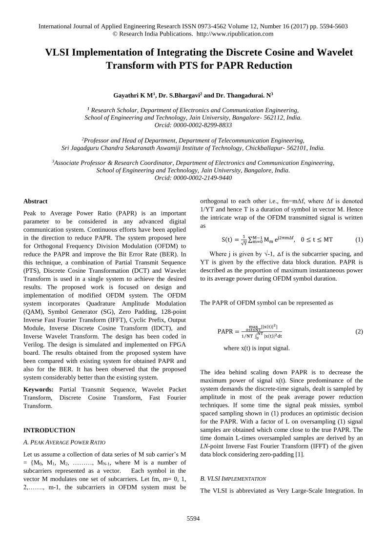
technology. Figure 1 shows the flow diagram of VLSI Design.
Figure 1: VLSI Design Flow
Though VLSI designs are successful, continues efforts are put
for improvements and advancements in increasing the number
of transistors per chip in the area of VLSI. This leads to
another technology called as ultra VLSI technologies. The
VLSI design is used to minimize the parameters like power
consumption, process variations and so on.
VHDL stands for Very high-speed IC Hardware Description
Language. It is used in electronic design automation to give
the description of digital systems such as field-programmable
gate arrays and integrated circuits. First, it entitles the
description of structure of the system, i.e., how a system is
disintegrated into sub-systems and how these sub-systems are
concatenated. Second, it allows specification of the function
of the system so that the designer knows what to do. Thirdly,
it defines the detailed structure of the system to be designed.
A Field-programmable Gate Array (FPGA) is an integrated
circuit designed to be configured by the designer after
manufacturing. The configuration of FPGA is generally using
a specified hardware description language (HDL), Any logical
function can be implemented using FPGAs. FPGA includes
programmable logic components such as "logic blocks", and a
hierarchy of reconfigurable interconnects that allow the blocks
to be "wired together". It is like numerous logic gates that can
be wired in different configurations. The simple and complex
combinational functions are performed by configuring the
logic blocks. In most of the FPGAs, the logic blocks also
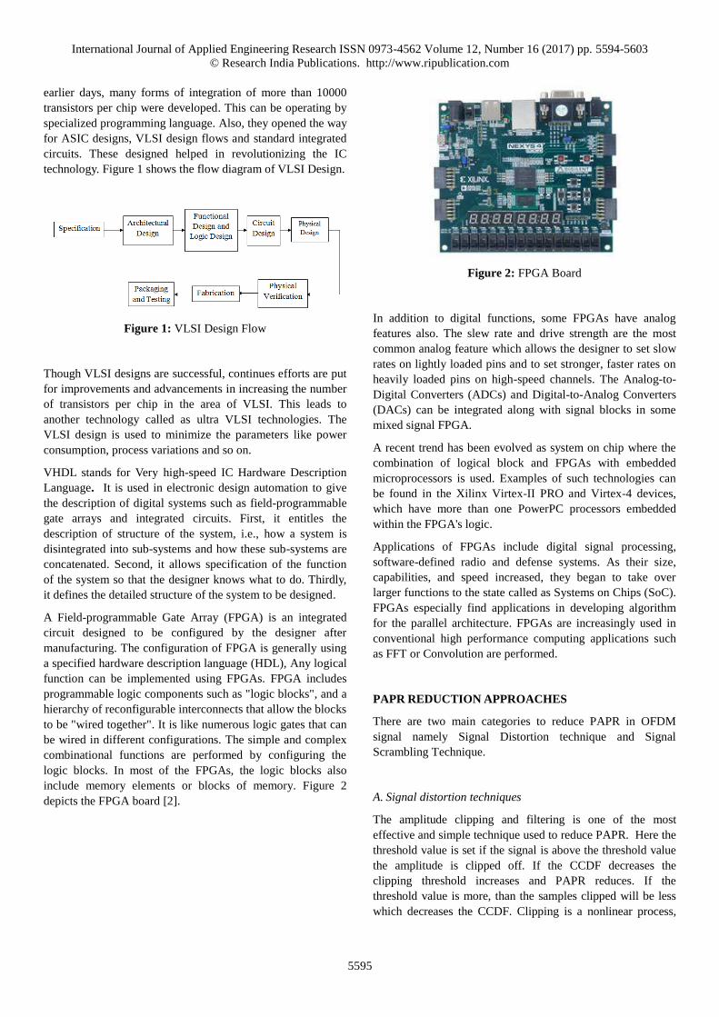
include memory elements or blocks of memory. Figure 2
depicts the FPGA board [2].
Figure 2: FPGA Board
In addition to digital functions, some FPGAs have analog
features also. The slew rate and drive strength are the most
common analog feature which allows the designer to set slow
rates on lightly loaded pins and to set stronger, faster rates on
heavily loaded pins on high-speed channels. The Analog-to-
Digital Converters (ADCs) and Digital-to-Analog Converters
(DACs) can be integrated along with signal blocks in some
mixed signal FPGA.
A recent trend has been evolved as system on chip where the
combination of logical block and FPGAs with embedded
microprocessors is used. Examples of such technologies can
be found in the Xilinx Virtex-II PRO and Virtex-4 devices,
which have more than one PowerPC processors embedded
within the FPGA's logic.
Applications of FPGAs include digital signal processing,
software-defined radio and defense systems. As their size,
capabilities, and speed increased, they began to take over
larger functions to the state called as Systems on Chips (SoC).
FPGAs especially find applications in developing algorithm
for the parallel architecture. FPGAs are increasingly used in
conventional high performance computing applications such
as FFT or Convolution are performed.
PAPR REDUCTION APPROACHES
There are two main categories to reduce PAPR in OFDM
signal namely Signal Distortion technique and Signal
Scrambling Technique.
A. Signal distortion techniques
The amplitude clipping and filtering is one of the most
effective and simple technique used to reduce PAPR. Here the
threshold value is set if the signal is above the threshold value
the amplitude is clipped off. If the CCDF decreases the
clipping threshold increases and PAPR reduces. If the
threshold value is more, than the samples clipped will be less
which decreases the CCDF. Clipping is a nonlinear process,
International Journal of Applied Engineering Research ISSN 0973-4562 Volume 12, Number 16 (2017) pp. 5594-5603
© Research India Publications. http://www.ripublication.com
5596
where the distortion is viewed as noise. The peak windowing is
one of the approaches used to reduce the PAPR. Here the
Gaussian shaped window is multiplied to a huge signal peak to
minimize PAPR. The obtained spectrum is a convolution of
indigenous OFDM and window spectrum. This technique
scales down PAPR at a demand of raise in bit error rate [2].
B. Signal scrambling techniques
To reduce PAPR the linear coding is also used. The key factor
to reduce PAPR is to select a proper codeword for
transmission. Coding scheme uses a known data block with
constellation modulation such as QPSK and PSK. The code
word which is having high peak power is blocked from
transmission. This method is useful only for limited number of
sub carriers where PAPR reduction is achieved.
The fundamental objective of tone injection approach is to
magnify the constellation size and map the indigenous
constellation into analogues points in that. For every symbol in
the data block there are many constellations which are mapped
in extended constellation. The amount of scaling down PAPR
is dependent on the modified symbols in the data block. As this
method occupies the same frequency band for injected signal,
it is more complicated when compared to tone reservation.
Due to injected signal, the power and the implementation
complexity increase [3-4].
Tone reservation is one of the efficient methods used for
minimization of PAPR. The idea in this technique is it reserves
the tone both at transmitter and receiver. In tone reservation,
the main aim is to find the value of time domain signal ‘C’
with the help of convex optimization problem which can be
solved using linear programming.
Equivalent to tone injection technique, Active constellation
technique is used for PAPR reduction. The outer signal
constellation is expanded toward outside of the indigenous
constellation so the PAPR is scaled down. This can be
implemented in different modulation techniques such as QAM,
QPSK and MPSK. The combination of additional signals can
be used for peak cancellation. This method reduces the bit
error rate and no side information is required for transmission.
But it demands for a larger constellation size modulation
technique [5-6]
Selected Mapping is one of the probabilistic schemes used for
PAPR reduction. This method generates parallel OFDM
signals in time domain which are asymptotically independent.
For these parallel input data, the phase sequence is multiplied
and then IFFT is applied for each data. Out of that the one
having a less PAPR is selected and transmitted. Each data
block is expanded with some sequences which results in ‘S’
different blocks of data. Along with these altered data block
the one with less PAPR is chosen for transmitted along with
the corresponding phase vector as side information. To recover
the original data, block the reserve operation is done. In order
to implement this method, we require S IFFT block and for
every data block the necessary side information is [𝑙𝑜𝑔2𝑆]. The
reduction of PAPR relies on the design of phase factor and
number of phase sequences. The improved version of SLM
technique is used to minimize PAPR [7-8][10].
In OFDM the powerful probabilistic based PAPR reduction
technique is Partial Transmit Sequence (PTS). In this scheme,
the original data X is divided into N non-overlapping sub
blocks. In each sub-block the sub carriers are weighted by a
phase factor. The selection of phase factors make sure that the
PAPR is reduced. The flow of PTS algorithm is a) The OFDM
sub carrier is split into M non-overlapping sub blocks. b) For
every sub block the OFDM signal is generated by taking
IFFT. c) The OFDM signal combined with weighted phase
factor bi. d) By using optimization algorithm the phase factors
are generated. e) To retrieve the data at the receiver, receiver
should know the generation scheme [12].
PROPOSED ALGORITHM
The binary data is the input to the OFDM system. The stream
of binary data is given to the convolution encoder. The
encoded samples are modulated using QAM modulator. After
modulation, the Discrete Cosine transform and Wavelet
transform is applied in order to reduce the PAPR of the
OFDM system. The output is then applied the conventional
OFDM and PTS technique. The output from PTS technique is
given to the AWGN channel and at the receiver end the
reverse process of the transmitter will be done and finally the
BER is calculated [9][11].
The FPGA flow involves the following steps:
Design Entry – to achieve the proposed system the
hardware description language such as Verilog is
used.
Synthesis – the proposed design is synthesized into a
hardware circuit that consists of the logic blocks.
Functional Simulation – the synthesized circuit is
verified with its functional working.
Implementation – the logical blocks are placed into
the actual FPGA with the help of netlist. It also
chooses routing wires in the chip to make the
required connections.
Programming and Configuration – the proposed
circuit is implemented in a physical FPGA chip by
programming the configuration switches that
configure the logical blocks and establish the
required wiring connections.
International Journal of Applied Engineering Research ISSN 0973-4562 Volume 12, Number 16 (2017) pp. 5594-5603
© Research India Publications. http://www.ripublication.com
5597
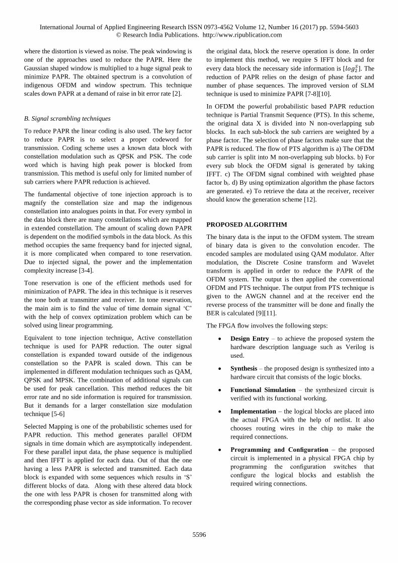
Input Binary stream
Apply Convolution Encoding
QAM-M Modulation
Apply DCT operation
OFDM Modulation
Partial Transmit Sequence
AWGN Channel
Apply Inverse Partial Transmit sequence
operation
OFDM De-Modulation
Apply IDCT operation
QAM-M De-Modulation
Apply Viterbi Decoder
Re arrange the Data to the Original
Format
Stop
Input Data in Binary format
Calculate
BER
Save
BER
Calculate
PAPR
Save
PAPR
Figure 3: Proposed algorithm flow
SIMULATION RESULTS
A. Conventional OFDM
Serial to parallel converter
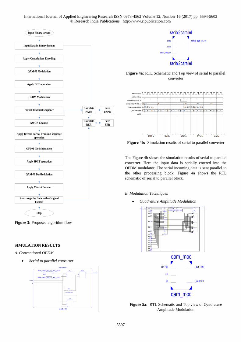
Figure 4a: RTL Schematic and Top view of serial to parallel
converter
Figure 4b: Simulation results of serial to parallel converter
The Figure 4b shows the simulation results of serial to parallel
converter. Here the input data is serially entered into the
OFDM modulator. The serial incoming data is sent parallel to
the other processing block. Figure 4a shows the RTL
schematic of serial to parallel block.
B. Modulation Techniques
Quadrature Amplitude Modulation
Figure 5a: RTL Schematic and Top view of Quadrature
Amplitude Modulation
International Journal of Applied Engineering Research ISSN 0973-4562 Volume 12, Number 16 (2017) pp. 5594-5603
© Research India Publications. http://www.ripublication.com
5598
Figure 5b: Simulation results of Quadrature Amplitude
Modulation
The Figure 5a shows the simulation results of QAM
modulation. Here the bits entering to the modulator is divided
into two equal parts namely quadrature and in phase which is
multiplied by cosine and sine values respectively. Figure 5b
shows the RTL schematic of QAM modulator.
Binary Phase Shift Keying
The Figure 6a shows the output wave form of the BPSK. As
the message signal changes from 1 to 0 or from 0 to 1 the
carrier wave will experience a phase shift of 180o. The Figure
6b shows the RTL schematic of BPSK. There are four
modules of BPSK each of 8 bits and the final BPSK output is
32 bits. The figure shows the top view of BPSK it has clock,
enable and data in as input pins and bpsk_out as output pin.
.
Figure 6a: RTL Schematic and Top view of Binary Phase
Shift Keying
Figure 6b: Simulation results of Binary Phase Shift Keying
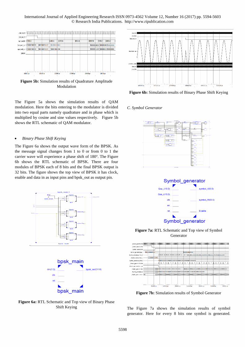
C. Symbol Generator
Figure 7a: RTL Schematic and Top view of Symbol
Generator
Figure 7b: Simulation results of Symbol Generator
The Figure 7a shows the simulation results of symbol
generator. Here for every 8 bits one symbol is generated.
International Journal of Applied Engineering Research ISSN 0973-4562 Volume 12, Number 16 (2017) pp. 5594-5603
© Research India Publications. http://www.ripublication.com
5599
Figure 7b shows the RTL schematic and top view of symbol
generator.
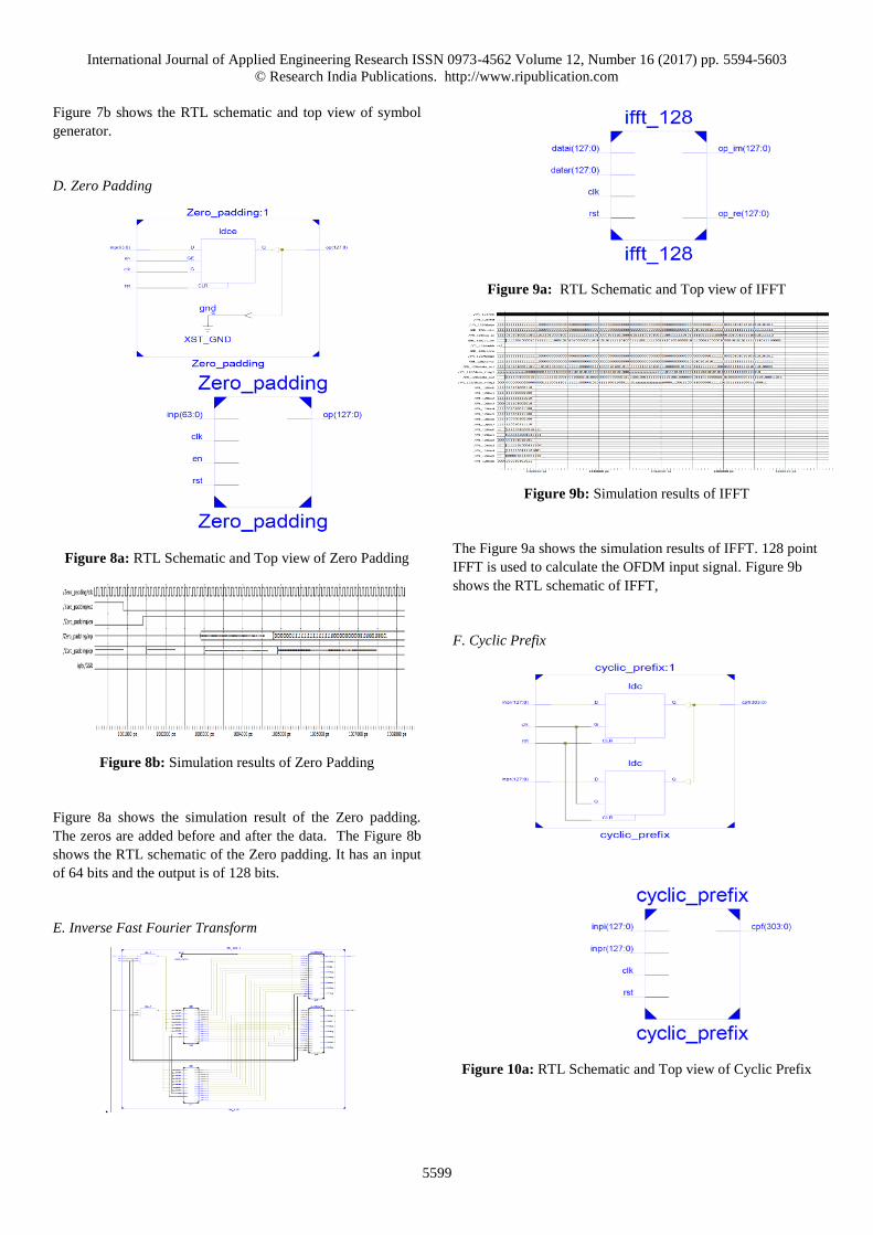
D. Zero Padding
Figure 8a: RTL Schematic and Top view of Zero Padding
Figure 8b: Simulation results of Zero Padding
Figure 8a shows the simulation result of the Zero padding.
The zeros are added before and after the data. The Figure 8b
shows the RTL schematic of the Zero padding. It has an input
of 64 bits and the output is of 128 bits.
E. Inverse Fast Fourier Transform
.
Figure 9a: RTL Schematic and Top view of IFFT
Figure 9b: Simulation results of IFFT
The Figure 9a shows the simulation results of IFFT. 128 point
IFFT is used to calculate the OFDM input signal. Figure 9b
shows the RTL schematic of IFFT,
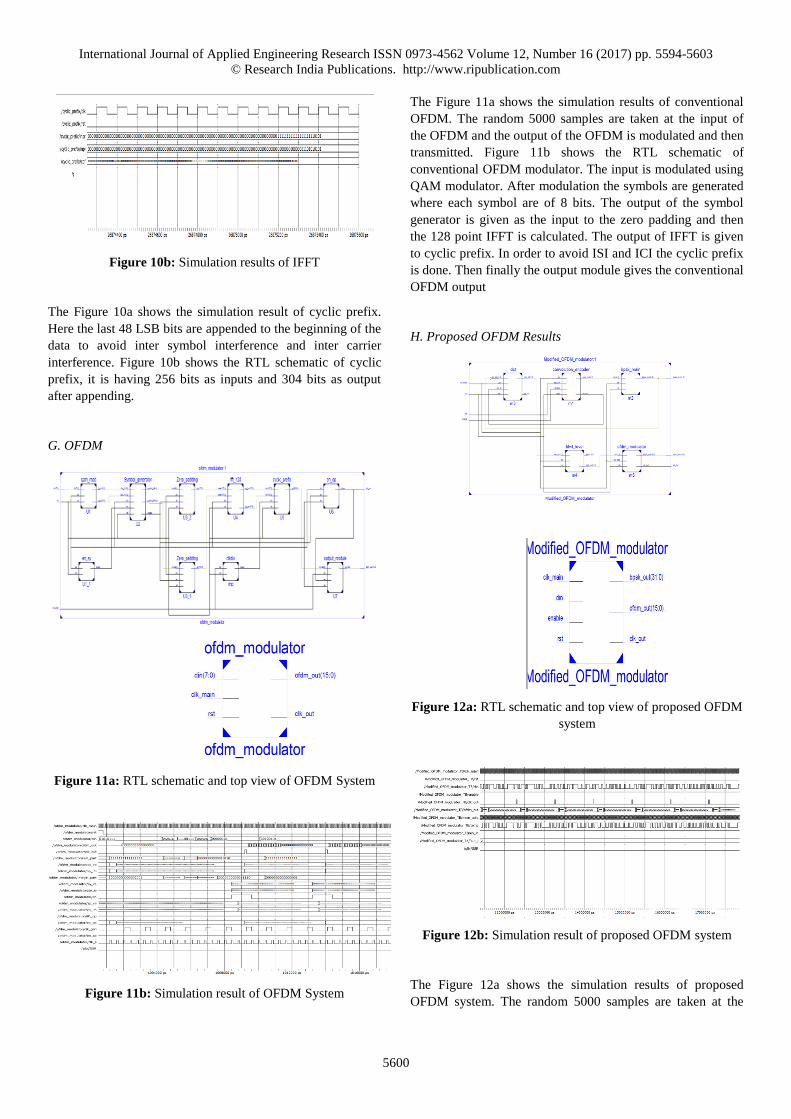
F. Cyclic Prefix
Figure 10a: RTL Schematic and Top view of Cyclic Prefix
International Journal of Applied Engineering Research ISSN 0973-4562 Volume 12, Number 16 (2017) pp. 5594-5603
© Research India Publications. http://www.ripublication.com
5600
Figure 10b: Simulation results of IFFT
The Figure 10a shows the simulation result of cyclic prefix.
Here the last 48 LSB bits are appended to the beginning of the
data to avoid inter symbol interference and inter carrier
interference. Figure 10b shows the RTL schematic of cyclic
prefix, it is having 256 bits as inputs and 304 bits as output
after appending.
G. OFDM
Figure 11a: RTL schematic and top view of OFDM System
Figure 11b: Simulation result of OFDM System
The Figure 11a shows the simulation results of conventional
OFDM. The random 5000 samples are taken at the input of
the OFDM and the output of the OFDM is modulated and then
transmitted. Figure 11b shows the RTL schematic of
conventional OFDM modulator. The input is modulated using
QAM modulator. After modulation the symbols are generated
where each symbol are of 8 bits. The output of the symbol
generator is given as the input to the zero padding and then
the 128 point IFFT is calculated. The output of IFFT is given
to cyclic prefix. In order to avoid ISI and ICI the cyclic prefix
is done. Then finally the output module gives the conventional
OFDM output
H. Proposed OFDM Results
Figure 12a: RTL schematic and top view of proposed OFDM
system
Figure 12b: Simulation result of proposed OFDM system
The Figure 12a shows the simulation results of proposed
OFDM system. The random 5000 samples are taken at the
International Journal of Applied Engineering Research ISSN 0973-4562 Volume 12, Number 16 (2017) pp. 5594-5603
© Research India Publications. http://www.ripublication.com
5601
input of the OFDM and the output of the OFDM is modulated
and then transmitted. Figure 12b shows the RTL schematic of
modified OFDM modulator. The input is given to the
convolution encoder. The output of convolution encoder is
modulated using BPSK. The output of the modulator is given
to the IDCT for auto correlation. The output of the IDCT is
given to the wavelet transforms and then the final output is
taken after the conventional OFDM modulator.
I. Convolution encoder
Figure 13a: RTL schematic and top view of convolution
encoder
Figure 13b: Simulation result of convolution encoder
Figure 13a shows the simulation of a convolution encoder. It
is a simplest way of channel encoding technique used for
AWGN channel. Here we have used a 1/3 convolution
encoder with a constraint length of 5 i.e., the five shift
registers are used to calculate the output. The Figure 13b
shows the RTL schematic of convolution encoder. The state
machine is used to code the encoder in verilog. The figure
shows the top view of convolution encoder it has clock,
enable and data in as input pins and code_out as output pin
which is 3 bits.
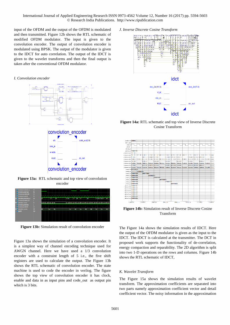
J. Inverse Discrete Cosine Transform
Figure 14a: RTL schematic and top view of Inverse Discrete
Cosine Transform
Figure 14b: Simulation result of Inverse Discrete Cosine
Transform
The Figure 14a shows the simulation results of IDCT. Here
the output of the OFDM modulator is given as the input to the
IDCT. The IDCT is calculated at the transmitter. The DCT in
proposed work supports the functionality of de-correlation,
energy compaction and reparability. The 2D algorithm is split
into two 1-D operations on the rows and columns. Figure 14b
shows the RTL schematic of IDCT,
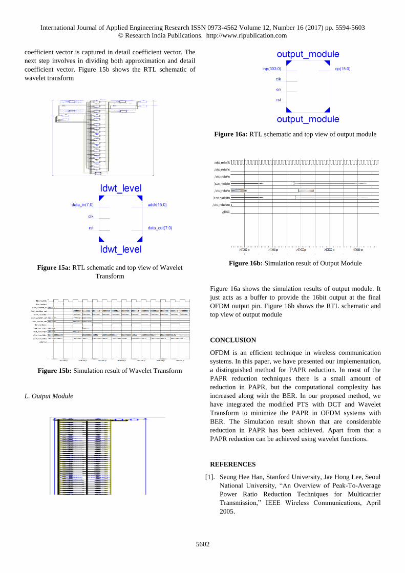
K. Wavelet Transform
The Figure 15a shows the simulation results of wavelet
transform. The approximation coefficients are separated into
two parts namely approximation coefficient vector and detail
coefficient vector. The noisy information in the approximation
International Journal of Applied Engineering Research ISSN 0973-4562 Volume 12, Number 16 (2017) pp. 5594-5603
© Research India Publications. http://www.ripublication.com
5602
coefficient vector is captured in detail coefficient vector. The
next step involves in dividing both approximation and detail
coefficient vector. Figure 15b shows the RTL schematic of
wavelet transform
Figure 15a: RTL schematic and top view of Wavelet
Transform
Figure 15b: Simulation result of Wavelet Transform
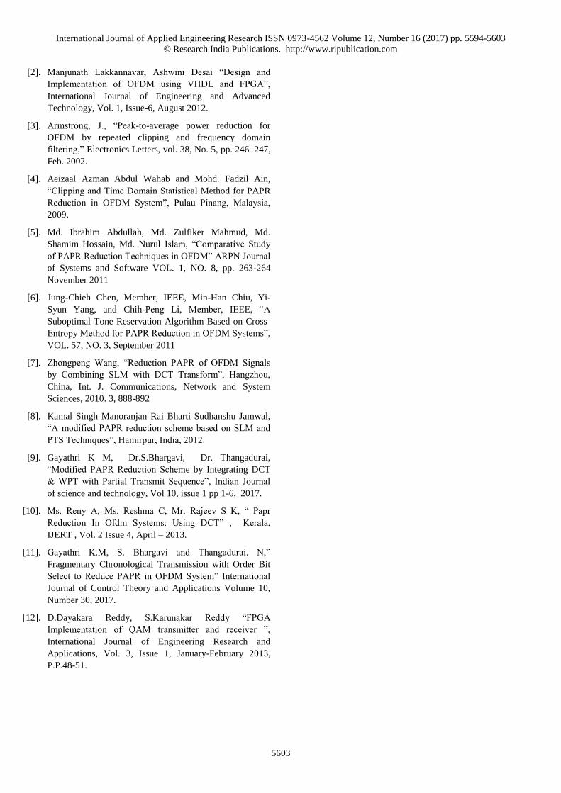
L. Output Module
Figure 16a: RTL schematic and top view of output module
Figure 16b: Simulation result of Output Module
Figure 16a shows the simulation results of output module. It
just acts as a buffer to provide the 16bit output at the final
OFDM output pin. Figure 16b shows the RTL schematic and
top view of output module
CONCLUSION
OFDM is an efficient technique in wireless communication
systems. In this paper, we have presented our implementation,
a distinguished method for PAPR reduction. In most of the
PAPR reduction techniques there is a small amount of
reduction in PAPR, but the computational complexity has
increased along with the BER. In our proposed method, we
have integrated the modified PTS with DCT and Wavelet
Transform to minimize the PAPR in OFDM systems with
BER. The Simulation result shown that are considerable
reduction in PAPR has been achieved. Apart from that a
PAPR reduction can be achieved using wavelet functions.
REFERENCES
[1]. Seung Hee Han, Stanford University, Jae Hong Lee, Seoul
National University, “An Overview of Peak-To-Average
Power Ratio Reduction Techniques for Multicarrier
Transmission,” IEEE Wireless Communications, April
2005.
International Journal of Applied Engineering Research ISSN 0973-4562 Volume 12, Number 16 (2017) pp. 5594-5603
© Research India Publications. http://www.ripublication.com
5603
[2]. Manjunath Lakkannavar, Ashwini Desai “Design and
Implementation of OFDM using VHDL and FPGA”,
International Journal of Engineering and Advanced
Technology, Vol. 1, Issue-6, August 2012.
[3]. Armstrong, J., “Peak-to-average power reduction for
OFDM by repeated clipping and frequency domain
filtering,” Electronics Letters, vol. 38, No. 5, pp. 246–247,
Feb. 2002.
[4]. Aeizaal Azman Abdul Wahab and Mohd. Fadzil Ain,
“Clipping and Time Domain Statistical Method for PAPR
Reduction in OFDM System”, Pulau Pinang, Malaysia,
2009.
[5]. Md. Ibrahim Abdullah, Md. Zulfiker Mahmud, Md.
Shamim Hossain, Md. Nurul Islam, “Comparative Study
of PAPR Reduction Techniques in OFDM” ARPN Journal
of Systems and Software VOL. 1, NO. 8, pp. 263-264
November 2011
[6]. Jung-Chieh Chen, Member, IEEE, Min-Han Chiu, Yi-
Syun Yang, and Chih-Peng Li, Member, IEEE, “A
Suboptimal Tone Reservation Algorithm Based on Cross-
Entropy Method for PAPR Reduction in OFDM Systems”,
VOL. 57, NO. 3, September 2011
[7]. Zhongpeng Wang, “Reduction PAPR of OFDM Signals
by Combining SLM with DCT Transform”, Hangzhou,
China, Int. J. Communications, Network and System
Sciences, 2010. 3, 888-892
[8]. Kamal Singh Manoranjan Rai Bharti Sudhanshu Jamwal,
“A modified PAPR reduction scheme based on SLM and
PTS Techniques”, Hamirpur, India, 2012.
[9]. Gayathri K M, Dr.S.Bhargavi, Dr. Thangadurai,
“Modified PAPR Reduction Scheme by Integrating DCT
& WPT with Partial Transmit Sequence”, Indian Journal
of science and technology, Vol 10, issue 1 pp 1-6, 2017.
[10]. Ms. Reny A, Ms. Reshma C, Mr. Rajeev S K, “ Papr
Reduction In Ofdm Systems: Using DCT” , Kerala,
IJERT , Vol. 2 Issue 4, April – 2013.
[11]. Gayathri K.M, S. Bhargavi and Thangadurai. N,”
Fragmentary Chronological Transmission with Order Bit
Select to Reduce PAPR in OFDM System” International
Journal of Control Theory and Applications Volume 10,
Number 30, 2017.
[12]. D.Dayakara Reddy, S.Karunakar Reddy “FPGA
Implementation of QAM transmitter and receiver ”,
International Journal of Engineering Research and
Applications, Vol. 3, Issue 1, January-February 2013,
P.P.48-51.