voltage regulation and reactive power compensation · pdf filevoltage regulation and reactive...
TRANSCRIPT
DOKUZ EYLÜL UNIVERSITY
GRADUATE SCHOOL OF NATURAL AND APPLIED SCIENCES
VOLTAGE REGULATION AND
REACTIVE POWER COMPENSATION
USING STATCOM
by
Abdül BALIKCI
February, 2014
İZMİR
VOLTAGE REGULATION AND
REACTIVE POWER COMPENSATION
USING STATCOM
A Thesis Submitted to the
Graduate School of Natural and Applied Sciences of Dokuz Eylül University
In Partial Fulfillment of the Requirements for the Degree of Doctor of
Philosophy in Electrical and Electronics Engineering,
Electrical and Electronics Program
by
Abdül BALIKCI
February, 2014
İZMİR

iii
ACKNOWLEDGMENTS
First and foremost, I express my deepest gratitude to my advisor Prof. Dr. Eyüp
AKPINAR for his guidance, support and advices at every stage of this dissertation.
His valuable insights, experiences, and encouragement will guide me in all aspects of
my academic life in the future.
This work has been carried out as a part of project sponsored by Turkish Scientific
and Research Council (TUBİTAK) under contract 110E205. I would like to thank
them for their financial support.
I would like to thank Asst. Prof. Dr. Kadir Vardar for his support on design of
prototype unit and I would like to thank Buket Turan Azizoğlu for her support on
simulation of PSPICE.
I would like to thank my Thesis Progress Committee member, namely Prof. Dr.
Coşkun Sarı and Asst. Prof. Dr. Tolga Sürgevil for their useful comments and
suggestions.
Finally, I express my gratitude to my family and especially to my little daughter
for their patience and moral support.
Abdül BALIKCI

iv
VOLTAGE REGULATION AND REACTIVE POWER COMPENSATION
USING STATCOM
ABSTRACT
In this thesis, a novel five level multilevel converter has been designed as
STATCOM application. Star or delta connected, five-level Static Synchronous
Compensator with reduced number of switches is proposed for compensation of
balanced and unbalanced loads. The active and reactive powers demanded by the
load are estimated by using two different methods that are single phase P-Q and
impedance matching methods. Firstly, single phase P-Q is applied on each phase
independently to compensate the reactive power from star-connected compensator.
Secondly, compensator is connected in delta-form to carry out load balancing with
reactive power compensation.
The system is implemented in the laboratory by using floating point DSP
TMS320F28335 central processor unit. The control algorithm is programmed in C
language by using Code Composer Studio compiler and is tested by co-operating
Matlab/Simulink with DSP. This interactive method assures elimination of
programming mistakes before implementation circuit. A dedicated model of single-
phase converter has been obtained at synchronously rotating reference frame. The
performance of proposed converter is compared with results of simulation, dedicated
model and implementation. A feed forward controller is designed by using dedicated
model to make system settle down in shorter time.
Finally, the novel converter is connected to grid first time for bi-directional
power control. All results from the dedicated model, Simulink and implementation
work are compared to each other and it is verified that this converter has all the
features of conventional H-bridge converter.
Keywords: Reactive Power Compensation, Digital signal processor, Single Phase P-
Q, Load Balancing, STATCOM, AC/DC Converter
v
GERİLİM DÜZENLEMESİ VE REAKTİF GÜÇ KOMPANZASYONUNDA
STATCOM UYGULAMASI
ÖZ
Bu tezde, STATCOM uygulamaları için beş seviyeli yeni konvertör yapısı
tasarlandı. Yarı iletken sayısı azaltılmış beş seviyeli STATCOM yıldız ve üçgen
bağlanılarak dengeli ve dengesiz yüklerin kompanzasyonu için önerilmektedir. Yük
tarafından talep edilen aktif ve reaktif yükler iki farklı metot kullanılarak
hesaplanmıştır, bunlar tek faz P-Q ve empedans eşleme metodudur. İlk olarak, her bir
fazdaki reaktif güç talebinin bağımsız olarak kompanze edildiği tek faz P-Q yıldız
bağlı kompanzatöre uygulandı. İkinci olarak, kompanzatör üçgen bağlanarak reaktif
güç kompanzasyonu yanında aktif yük dengelemesi yapılmıştır.
Sistem kayar noktalı DSP TMS320F28335 merkezi işlem birimi kullanılarak
laboratuvarda uygulanmıştır. Kontrol algoritması Code Composer Studio derleyicisi
kullanılarak C programlama dilinde yazılmış ve Matlab/Simulink ve DSP’nin ortak
çalıştırılmasıyla yazılan program kodu test edilmiştir. Bu etkileşimli metot uygulama
devresi öncesi programlama hatalarının giderilmesini garanti etmektedir. Tek faz
konvertöre ait model senkron hızda dönen referans düzlemde elde edilmiştir.
Önerilen konvertörün performansı benzetim, model ve uygulama sonuçları
kullanılarak karşılaştırılmıştır. Konvertöre özel model kullanılarak sistemin daha
hızlı kararlı hale gelmesi ileri beslemeli denetleyici tasarlanarak sağlanmıştır.
Sonuç olarak, yeni tasarlanan konvertör ilk kez şebekeye bağlanmış ve iki yönlü
güç akışı yapması sağlanmıştır. Önerilen konvertöre ait benzetim, model ve
uygulama sonuçları birbirine göre karşılaştırılmış ve sonuç olarak önerilen
konvertörün geleneksel H- köprü yapısına sahip konvertörün tüm özelliklerine sahip
olduğu doğrulanmıştır.
Anahtar Kelimeler: Reaktif güç kompanzasyonu, Sayısal işaret işleyicisi, Tek faz
P-Q, Yük dengeleme, STATCOM, AC/DC dönüştürücü
vi
CONTENTS
Page
THESIS EXAMINATION RESULT FORM .............................................................. ii
ACKNOWLEDGEMENTS ........................................................................................ iii
ABSTRACT ................................................................................................................ iv
ÖZ ................................................................................................................................ v
LIST OF FIGURES ................................................................................................... xi
LIST OF TABLES .................................................................................................. xxii
CHAPTER ONE – INTRODUCTION .................................................................... 1
CHAPTER TWO – REACTIVE POWER AND COMPENSATION .................. 6
2.1 FACTS Concepts ............................................................................................... 6
2.2 Shunt Connected Controller .............................................................................. 7
2.2.1 Static VAR Compensators ......................................................................... 8
2.2.2 Static Synchronous Compensator (STATCOM) ........................................ 9
2.3 Reactive Power Compensation Using Shunt Connected STATCOM ............ 10
2.4 Estimation of Instantaneous Reactive Power .................................................. 14
2.4.1 Three Phase Instantaneous Reactive Power Theory ................................ 14
2.4.2 Single Phase Instantaneous Reactive Power Theory ............................... 15
2.5 Investigation of Single Phase P-Q with Distorted Waveform ......................... 17
2.5.1 Investigation of Single Phase P-Q with only Current Harmonics............ 17
CHAPTER THREE – PROPOSED MULTILEVEL CONVERTER ................. 20
3.1 Introductory Remarks ...................................................................................... 20
3.2 Type of Multilevel Converters as STATCOM ................................................ 21
3.2.1 Diode-Clamped Multilevel Converter ..................................................... 21
3.2.2 Flying-Capacitor Multilevel Converter .................................................... 22
vii
3.2.3 Cascaded-Multilevel Converters .............................................................. 24
3.2.4 Modular Multilevel Converter ................................................................. 25
3.3 General Appearance of Proposed Converter ................................................... 27
3.4 Switching States of Proposed Converter ......................................................... 29
3.5 Discussing on Employed Modulation Techniques for Proposed Converter ... 33
3.5.1 Selective Harmonic Elimination Methods ............................................... 34
3.5.2 STATCOM Application with Selective Harmonic Elimination .............. 38
3.5.2.1 Delta Connected Operation ............................................................. 38
3.5.2.2 Star Connected Operation ............................................................... 43
3.5.3 Sinusoidal Pulse Width Modulation (SPWM) Method ............................ 45
3.5.4 Simulation and Experimental Verification of SPWM on Converter ....... 51
3.6 DC Capacitor Voltage Balancing .................................................................... 54
3.7 Power Losses of Proposed Converter .............................................................. 58
CHAPTER FOUR – DESIGN OF THREE PHASE MULTILEVEL STATCOM
.................................................................................................................................... 61
4.1 Introductory Remarks ...................................................................................... 61
4.2 Hardware Design ............................................................................................. 61
4.2.1 Design of Main Control Cards ................................................................. 61
4.2.2 Design of Snubber Circuit ........................................................................ 70
4.3 Software Design .............................................................................................. 73
4.3.1 General Control Algorithm ...................................................................... 73
4.3.2 Design of PLL .......................................................................................... 75
4.3.3 Application of Digital PI Controller ........................................................ 76
4.3.4 Design of DC Link Voltage Controller .................................................... 77
4.3.5 Programming of Single Phase P-Q .......................................................... 78
4.3.6 Execution Times of Program Code .......................................................... 79
4.3.7 Checking Program code with Co-operation of Matlab/Simulink and
DSP ................................................................................................................... 80
viii
CHAPTER FIVE – MODELLING OF STATCOM............................................. 82
5.1 Introductory Remarks ...................................................................................... 82
5.2 Single Phase Transformation from - to d-q Axis ........................................ 83
5.3 Switching Functions ........................................................................................ 88
5.4 Comparing Results of Model and Matlab Simulation ..................................... 92
CHAPTER SIX – REACTIVE POWER COMPENSATION WITH STATCOM
USING SINGLE PHASE P-Q ................................................................................. 97
6.1 Introductory Remarks ...................................................................................... 97
6.2 Star Connection of STATCOM with Neutral Line ......................................... 98
6.2.1 Balance Load in Parallel to Star-Connected STATCOM ........................ 99
6.2.1.1 Balance R-L Load in Parallel to Star-Connected STATCOM ...... 100
6.2.1.2 Balance R-C Load in Parallel to Star-Connected STATCOM...... 102
6.2.1.3 Balance R Load in Parallel to Star-Connected STATCOM.......... 103
6.2.1.4 Balance L Load in Parallel to Star-Connected STATCOM .......... 105
6.2.1.5 Balance C Load in Parallel to Star-Connected STATCOM.......... 107
6.2.2 Unbalanced Load in Parallel to Star-Connected STATCOM ................ 108
6.2.2.1 Unbalanced R-L Load with Star-Connected STATCOM ............. 109
6.2.2.2 Unbalanced R-C Load with Star-Connected STATCOM ............. 110
6.2.2.3 Unbalanced R Load with Star-Connected STATCOM ................. 111
6.2.2.4 Unbalanced L Load with Star-Connected STATCOM ................. 113
6.2.2.5 Unbalanced C Load with Star-Connected STATCOM ................. 114
6.2.3 Evaluation of Star-Connected Converter as STATCOM ....................... 115
6.3 Basic Circuit Configuration of Delta-Connected STATCOM ...................... 116
6.3.1 Balanced Loading Condition for Delta-Connected STATCOM ............ 120
6.3.1.1 Balanced R-L load on Delta-Connected STATCOM ................... 120
6.3.1.2 Balanced R-C load on Delta-Connected STATCOM ................... 122
6.3.1.3 Balanced R load on Delta-Connected STATCOM ....................... 124
6.3.1.4 Balanced L load on Delta-Connected STATCOM ....................... 125
6.3.1.5 Balanced C load on Delta-Connected STATCOM ....................... 127
ix
6.3.2 Unbalanced Loading Conditions for Delta-Connected STATCOM ...... 129
6.3.2.1 Unbalanced R-L load on Delta-Connected STATCOM ............... 130
6.3.2.2 Unbalanced R-C load on Delta-Connected STATCOM ............... 131
6.3.2.3 Unbalanced R load on Delta-Connected STATCOM ................... 132
6.3.2.4 Unbalanced L load on Delta-Connected STATCOM ................... 133
6.3.2.5 Unbalanced C load on Delta-Connected STATCOM ................... 135
6.3.3 Evaluation of Delta-Connected Proposed Converter as STATCOM ..... 136
CHAPTER SEVEN – LOAD BALANCING WITH STATCOM ..................... 137
7.1 Introductory Remarks .................................................................................... 137
7.2 Basic Circuit Configuration of Delta-Connected Compensator .................... 138
7.3 Impedance Matching Method for Delta-Connected Compensator ................ 139
7.3.1 Controlling Susceptance Value of STATCOM...................................... 139
7.3.2 Reactive Power Compensation and Load Balancing ............................. 140
7.4 Balanced Loading Condition for Delta-connected STATCOM .................... 150
7.4.1 Balanced R-L load on Delta-Connected STATCOM ............................ 151
7.4.2 Balanced R-C load on Delta-Connected STATCOM ............................ 152
7.4.3 Balanced R load on Delta-Connected STATCOM ................................ 154
7.4.4 Balanced L load on Delta-Connected STATCOM ................................ 156
7.4.5 Balanced C load on Delta-Connected STATCOM ................................ 157
7.5 Unbalanced Loading Condition for Delta-connected STATCOM ................ 159
7.5.1 Unbalanced R-L load on Delta-Connected STATCOM ........................ 160
7.5.2 Unbalanced R-C load on Delta-Connected STATCOM ........................ 161
7.5.3 Unbalanced R load on Delta-Connected STATCOM ............................ 162
7.5.4 Unbalanced L load on Delta-Connected STATCOM ............................ 163
7.5.5 Unbalanced C load on Delta-Connected STATCOM ............................ 155
7.6 Evaluation of Delta-Connected Proposed Converter as STATCOM ............ 166
CHAPTER EIGHT – CONCLUSIONS ............................................................... 167

x
REFERENCES ....................................................................................................... 170
APPENDICES ........................................................................................................ 177
xi
LIST OF FIGURES
Figure 2.1 Types of Facts controller a) Series controller b) Shunt controller c)
Combined series-series controller d) Combined series-shunt controller 7
Figure 2.2 Reactive power compensation units ....................................................... 8
Figure 2.3 Basic connection of STATCOM to AC ................................................ 10
Figure 2.4 Phasor diagrams of STATCOM on capacitive Mode .......................... 11
Figure 2.5 Phasor diagrams of STATCOM on inductive Mode ........................... 11
Figure 2.6 Phasor diagrams of STATCOM on capacitive Mode with power
angle. .................................................................................................. 13
Figure 2.7 Phasor diagrams of STATCOM on inductive Mode with power angle
........................................................................................................... 13
Figure 2.8 Reactive power calculation in single phase P-Q algorithm under pure
sinusoidal waveforms ......................................................................... 18
Figure 2.9 Reactive power calculation in single phase P-Q algorithm under non-
sinusoidal waveforms ........................................................................ 19
Figure 3.1 Five level diode-clamped multilevel converter for three-phase .......... 21
Figure 3.2 Five level flying capacitor multilevel converter for three-phase ......... 23
Figure 3.3 a) Single phase H-Bridge cell b) Cascaded converter cell .................. 24
Figure 3.4 Three-phase connection of modular multilevel converter ................... 26
Figure 3.5 a) Proposed multilevel converter b) Cascaded multilevel converter ... 27
Figure 3.6 Comparison of multilevel converter in terms of power component
requirements per phase ....................................................................... 29
Figure 3.7 Current paths of the proposed converter when input voltage is a) 2Vdc
b) -2Vdc c) Vdc d) -Vdc e) zero with left side f) zero with right side 30
Figure 3.8 PSPICE simulation results of IGBT gate pulses in sequence S1 through
S6 for fundamental switching conditions ........................................... 32
Figure 3.9 PSPICE simulation result of output voltage waveform of proposed
converter for fundamental switching conditions ................................ 32
Figure 3.10 Experimental results of IGBT gate pulses and output voltage waveform
of proposed converter for fundamental switching conditions ............ 33
xii
Figure 3.11 a) Output voltage waveform of converter b) V1 c) V2 d) V3 e) V4 f) V5
g) V6 ...................................................................................................... 35
Figure 3.12 Delta-connected configuration of STATCOM .................................... 36
Figure 3.13 Calculated firing angle versus modulation index ................................ 39
Figure 3.14 Output voltage waveform of converter and its FFT ............................ 39
Figure 3.15 Control schematic of delta connected STATCOM .............................. 40
Figure 3.16 Matlab/Simulink-DSP Co-operation result at inductive load a)Reactive
power b) STATCOM voltage¤t c) Source voltage¤t d)
DC link voltages ................................................................................. 41
Figure 3.17 Matlab/Simulink-DSP Co-operation result at capacitive load a)Reactive
power b)STATCOM voltage¤t c)Source voltage¤t d)DC
link voltages........................................................................................ 42
Figure 3.18 Calculated firing angle versus modulation index ................................ 43
Figure 3.19 Output voltage waveform of converter for elimination fifth harmonic 43
Figure 3.20 Control schematic of star-connected STATCOM ............................... 44
Figure 3.21 Experimental result at no-load a)Source current b)STATCOM voltage
c)Source voltage ................................................................................. 45
Figure 3.22 Kind of level shifted carrier based SPWM a) Phase Disposition (PD) b)
Phase Opposite Disposition (POD) c) Alternative Phase Opposition
Disposition (APOD) ........................................................................... 46
Figure 3.23 Harmonic analysis of STATCOM output voltage with SPWM method
............................................................................................................ 47
Figure 3.24 Level shifted carrier based SPWM .................................................... 48
Figure 3.25 Level shifted carrier based SPWM comparison logic and generated gate
signal ..................................................................................................... 48
Figure 3.26 a) Proposed multilevel converter b) Cascaded multilevel converter .... 49
Figure 3.27 Switching logic of conventional five level cascaded multilevel
converter ................................................................................................ 50
Figure 3.28 Switching logic of proposed five level multilevel converter ................ 51
Figure 3.29 Control schematic of star connected STATCOM ................................. 52
Figure 3.30 Simulation result at no-load a)Source current b)STATCOM voltage
c)DC link voltage (C1) d)DC link voltage (C2).................................... 53
xiii
Figure 3.31 Experimental result at no-load a)Source current b)STATCOM voltage
c)DC link voltage (C1) d)DC link voltage (C2) ..................................... 53
Figure 3.32 DC link capacitor rotating algorithm ..................................................... 55
Figure 3.33 Switching conditions for swapping algorithm a) Converter output voltage
is Vdc b) Converter output voltage is –Vdc .......................................... 55
Figure 3.34 DC link capacitor charge and discharge with load angle ...................... 56
Figure 3.35 a) DC link capacitor voltages for phase A b) Capacitor voltages under
no-load condition c) Capacitor voltages under R-L load d) Capacitor
voltages under R-C load ........................................................................ 57
Figure 3.36 Experimental result of swapping algorithm a) Source current b)
STATCOM voltage c) Capacitor 1 for phase A d) Capacitor 2 for
phase A .................................................................................................. 58
Figure 3.37 Number of conducted components in multilevel converter topologies per
phase ...................................................................................................... 59
Figure 3.38 Peak inverse voltages of proposed converter......................................... 60
Figure 4.1 a) Photography of power semiconductor b) Circuit diagram ............... 62
Figure 4.2 Voltage transducer circuit ..................................................................... 63
Figure 4.3 Three-phase supply voltage measurements card .................................. 64
Figure 4.4 DC link voltage measurements card ..................................................... 64
Figure 4.5 Current transducer circuit ..................................................................... 65
Figure 4.6 Three-phase supply current measurements card ................................... 65
Figure 4.7 Voltage conditioning card..................................................................... 66
Figure 4.8 Current conditioning card ..................................................................... 66
Figure 4.9 DSP and main control card ................................................................... 67
Figure 4.10 IGBT protection card ............................................................................ 68
Figure 4.11 IGBT protection card and Skyper 32 Pro R ......................................... 68
Figure 4.12 Completed installation of STATCOM. ................................................ 69
Figure 4.13 Proposed converter with snubber circuit .............................................. 70
Figure 4.14 a) Snubber current in simulation from PSPICE b) Snubber current in
experiment ............................................................................................. 71
Figure 4.15 a) Simulation from PSPICE and experimental results between collector-
emitter voltage of IGBTs without snubber b) Simulation from PSPICE
xiv
and experimental results between collector-emitter voltages of IGBTs
with snubber .......................................................................................... 72
Figure 4.16 General control algorithm of STATCOM ............................................ 74
Figure 4.17 Block diagram of traditional PLL ......................................................... 76
Figure 4.18 Block diagram of PI controller. ............................................................ 77
Figure 4.19 Charging resistor connection in star connected STATCOM ................ 77
Figure 4.20 First order low pass digital filter ........................................................... 78
Figure 4.21 Bode plot of first order low pass digital filter ...................................... 79
Figure 4.22 Matlab/Simulink and DSP28335 CCS interface................................... 81
Figure 5.1 Circuit diagram of three-phase STATCOM with neutral connection .. 84
Figure 5.2 Block diagram of d-q model of single phase STATCOM .................... 87
Figure 5.3 Switching function a)2Vdc b)Vdc c)-Vdc d) -2Vdc............................. 89
Figure 5.4 Model of single phase STATCOM ....................................................... 91
Figure 5.5 Comparison of mathematical model and simulation result a)reactive load
b)capacitor voltages c)Peak value of STATCOM voltage per phase
d)Peak value of STATCOM current per phase ..................................... 93
Figure 5.6 Mathematical model d-q parameters a) reactive load b) d-q components
of STATCOM voltage c) d-q components of STATCOM current d) d-q
components of switching functions ....................................................... 94
Figure 5.7 Feed forward control............................................................................. 95
Figure 5.8 Results from dedicated model and simulation under feed forward control
a) Reactive load b) Capacitor voltages c) Peak value of STATCOM
voltage per phase d) Peak value of STATCOM current per phase ....... 96
Figure 6.1 Control schematic of star with neutral connected STATCOM ............ 99
Figure 6.2 Simulation and implementation result from balanced R-L load a)
STATCOM voltage (V) b) Source voltage (V) c) Source current (A) d)
STATCOM current (A) ....................................................................... 101
Figure 6.3 Power & Energy measurement a) STATCOM is disconnected b)
STATCOM is connected c) Harmonic content of source current ....... 101
Figure 6.4 Transient response of STATCOM with balanced R-L load a) DC link
voltage (V) b) STATCOM voltage (V) c) Source current (A) d)
STATCOM current (A) ....................................................................... 101
xv
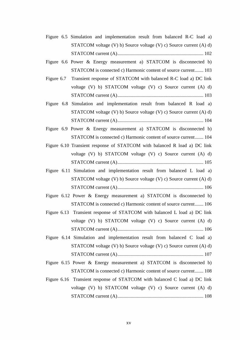
Figure 6.5 Simulation and implementation result from balanced R-C load a)
STATCOM voltage (V) b) Source voltage (V) c) Source current (A) d)
STATCOM current (A) ....................................................................... 102
Figure 6.6 Power & Energy measurement a) STATCOM is disconnected b)
STATCOM is connected c) Harmonic content of source current ....... 103
Figure 6.7 Transient response of STATCOM with balanced R-C load a) DC link
voltage (V) b) STATCOM voltage (V) c) Source current (A) d)
STATCOM current (A) ....................................................................... 103
Figure 6.8 Simulation and implementation result from balanced R load a)
STATCOM voltage (V) b) Source voltage (V) c) Source current (A) d)
STATCOM current (A) ....................................................................... 104
Figure 6.9 Power & Energy measurement a) STATCOM is disconnected b)
STATCOM is connected c) Harmonic content of source current ....... 104
Figure 6.10 Transient response of STATCOM with balanced R load a) DC link
voltage (V) b) STATCOM voltage (V) c) Source current (A) d)
STATCOM current (A) ....................................................................... 105
Figure 6.11 Simulation and implementation result from balanced L load a)
STATCOM voltage (V) b) Source voltage (V) c) Source current (A) d)
STATCOM current (A) ....................................................................... 106
Figure 6.12 Power & Energy measurement a) STATCOM is disconnected b)
STATCOM is connected c) Harmonic content of source current ....... 106
Figure 6.13 Transient response of STATCOM with balanced L load a) DC link
voltage (V) b) STATCOM voltage (V) c) Source current (A) d)
STATCOM current (A) ....................................................................... 106
Figure 6.14 Simulation and implementation result from balanced C load a)
STATCOM voltage (V) b) Source voltage (V) c) Source current (A) d)
STATCOM current (A) ....................................................................... 107
Figure 6.15 Power & Energy measurement a) STATCOM is disconnected b)
STATCOM is connected c) Harmonic content of source current ....... 108
Figure 6.16 Transient response of STATCOM with balanced C load a) DC link
voltage (V) b) STATCOM voltage (V) c) Source current (A) d)
STATCOM current (A) ....................................................................... 108

xvi
Figure 6.17 Simulation and implementation result from unbalanced R-L load a)
STATCOM voltage (V) b) Source voltage (V) c) Source current (A) d)
STATCOM current (A) ....................................................................... 110
Figure 6.18 Power & Energy measurement a) STATCOM is disconnected b)
STATCOM is connected c) Harmonic content of source current ....... 110
Figure 6.19 Simulation and implementation result from unbalanced R-C load a)
STATCOM voltage (V) b) Source voltage (V) c) Source current (A) d)
STATCOM current (A) ....................................................................... 111
Figure 6.20 Power & Energy measurement a) STATCOM is disconnected b)
STATCOM is connected c) Harmonic content of source current ....... 111
Figure 6.21 Simulation and implementation result from unbalanced R load a)
STATCOM voltage (V) b) Source voltage (V) c) Source current (A) d)
STATCOM current (A) ....................................................................... 112
Figure 6.22 Power & Energy measurement a) STATCOM is disconnected b)
STATCOM is connected c) Harmonic content of source current ....... 112
Figure 6.23 Simulation and implementation result from unbalanced L load a)
STATCOM voltage (V) b) Source voltage (V) c) Source current (A) d)
STATCOM current (A) ....................................................................... 113
Figure 6.24 Power & Energy measurement a) STATCOM is disconnected b)
STATCOM is connected c) Harmonic content of source current ....... 113
Figure 6.25 Simulation and implementation result from unbalanced C load a)
STATCOM voltage (V) b) Source voltage (V) c) Source current (A) d)
STATCOM current (A) ....................................................................... 114
Figure 6.26 Power & Energy measurement a) STATCOM is disconnected b)
STATCOM is connected c) Harmonic content of source current ....... 115
Figure 6.27 Control schematic of delta-connected STATCOM ........................... 117
Figure 6.28 Simulation and implementation result from balanced R-L load a)
STATCOM voltage (V) b) Source voltage (V) c) Source current (A) d)
STATCOM current (A) ....................................................................... 121
Figure 6.29 Power & Energy measurement a) STATCOM is disconnected b)
STATCOM is connected c) Harmonic content of source current ....... 121
xvii
Figure 6.30 Transient response of STATCOM with balanced R-L load a) DC link
voltage (V) b) STATCOM voltage (V) c) Source current (A) d)
STATCOM current (A) ....................................................................... 122
Figure 6.31 Simulation and implementation result from balanced R-C load a)
STATCOM voltage (V) b) Source voltage (V) c) Source current (A) d)
STATCOM current (A) ....................................................................... 123
Figure 6.32 Power & Energy measurement a) STATCOM is disconnected b)
STATCOM is connected c) Harmonic content of source current ....... 123
Figure 6.33 Transient response of STATCOM with balanced R-C load a) DC link
voltage (V) b) STATCOM voltage (V) c) Source current (A) d)
STATCOM current (A) ....................................................................... 123
Figure 6.34 Simulation and implementation result from balanced R load a)
STATCOM voltage (V) b) Source voltage (V) c) Source current (A) d)
STATCOM current (A) ....................................................................... 124
Figure 6.35 Power & Energy measurement a) STATCOM is disconnected b)
STATCOM is connected c) Harmonic content of source current ....... 125
Figure 6.36 Transient response of STATCOM with balanced R load a) DC link
voltage (V) b) STATCOM voltage (V) c) Source current (A) d)
STATCOM current (A) ....................................................................... 125
Figure 6.37 Simulation and implementation result from balanced L load a)
STATCOM voltage (V) b) Source voltage (V) c) Source current (A) d)
STATCOM current (A) ....................................................................... 126
Figure 6.38 Power & Energy measurement a) STATCOM is disconnected b)
STATCOM is connected c) Harmonic content of source current ....... 126
Figure 6.39 Transient response of STATCOM with balanced L load a) DC link
voltage (V) b) STATCOM voltage (V) c) Source current (A) d)
STATCOM current (A) ....................................................................... 127
Figure 6.40 Simulation and implementation result from balanced C load a)
STATCOM voltage (V) b) Source voltage (V) c) Source current (A) d)
STATCOM current (A) ....................................................................... 128
Figure 6.41 Power & Energy measurement a) STATCOM is disconnected b)
STATCOM is connected c) Harmonic content of source current ....... 128
xviii
Figure 6.42 Transient response of STATCOM with balanced C load a) DC link
voltage (V) b) STATCOM voltage (V) c) Source current (A) d)
STATCOM current (A) ....................................................................... 129
Figure 6.43 Simulation and implementation result from unbalanced R-L load a)
STATCOM voltage (V) b) Source voltage (V) c) Source current (A) d)
STATCOM current (A) ....................................................................... 130
Figure 6.44 Power & Energy measurement a) STATCOM is disconnected b)
STATCOM is connected c) Harmonic content of source current ....... 131
Figure 6.45 Simulation and implementation result from unbalanced R-C load a)
STATCOM voltage (V) b) Source voltage (V) c) Source current (A) d)
STATCOM current (A) ....................................................................... 132
Figure 6.46 Power & Energy measurement a) STATCOM is disconnected b)
STATCOM is connected c) Harmonic content of source current ....... 132
Figure 6.47 Simulation and implementation result from unbalanced R load a)
STATCOM voltage (V) b) Source voltage (V) c) Source current (A) d)
STATCOM current (A) ....................................................................... 133
Figure 6.48 Power & Energy measurement a) STATCOM is disconnected b)
STATCOM is connected c) Harmonic content of source current ....... 133
Figure 6.49 Simulation and implementation result from unbalanced L load a)
STATCOM voltage (V) b) Source voltage (V) c) Source current (A) d)
STATCOM current (A) ....................................................................... 134
Figure 6.50 Power & Energy measurement a) STATCOM is disconnected b)
STATCOM is connected c) Harmonic content of source current ....... 134
Figure 6.51 Simulation and implementation result from unbalanced R-L load a)
STATCOM voltage (V) b) Source voltage (V) c) Source current (A) d)
STATCOM current (A) ....................................................................... 135
Figure 6.52 Power & Energy measurement a) STATCOM is disconnected b)
STATCOM is connected c) Harmonic content of source current ....... 135
Figure 7.1 Control schematic of delta-connected STATCOM .............................. 138
Figure 7.2 Equivalent circuits of STATCOM ........................................................ 139
Figure 7.3 Delta-connected configuration of proposed converter as STATCOM . 141
Figure 7.4 Three-phase wye connected load .......................................................... 142

xix
Figure 7.5 Three-phase delta equivalent of load .................................................... 143
Figure 7.6 Parallel connected compensation susceptance...................................... 144
Figure 7.7 Parallel connected compensation susceptance in delta connection ...... 144
Figure 7.8 Compensated unbalanced real load ...................................................... 144
Figure 7.9 a) Single phase unbalanced load between phase A and B b) Compensated
single phase load with connecting capacitor and inductor .................. 145
Figure 7.10 Compensated load between phase A and B ......................................... 145
Figure 7.11 a) Single phase unbalanced load between phase B and C b) Compensated
single phase load with connecting capacitor and inductor c)
Compensated load between phase B and C......................................... 146
Figure 7.12 a) Single phase unbalanced load between phase C and A b) Compensated
single phase load with connecting capacitor and inductor c)
Compensated load between phase C and A ........................................ 147
Figure 7.13 a) Application of single phase load balancing b) Compensated single
phase load ............................................................................................ 148
Figure 7.14 Delta-connected compensator and unbalanced load ............................ 148
Figure 7.15 Simulation and implementation result from balanced R-L load a)
STATCOM voltage (V) b) Source voltage (V) c) Source current (A) d)
STATCOM current (A) ....................................................................... 151
Figure 7.16 Power & Energy measurement a) STATCOM is disconnected b)
STATCOM is connected c) Harmonic content of source current ....... 152
Figure 7.17 Transient response of STATCOM with balanced R-L load a) DC link
voltage (V) b) STATCOM voltage (V) c) Source current (A) d)
STATCOM current (A) ....................................................................... 152
Figure 7.18 Simulation and implementation result from balanced R-C load a)
STATCOM voltage (V) b) Source voltage (V) c) Source current (A) d)
STATCOM current (A) ....................................................................... 153
Figure 7.19 Power & Energy measurement a) STATCOM is disconnected b)
STATCOM is connected c) Harmonic content of source current ....... 153
Figure 7.20 Transient response of STATCOM with balanced R-C load a) DC link
voltage (V) b) STATCOM voltage (V) c) Source current (A) d)
STATCOM current (A) ....................................................................... 154
xx
Figure 7.21 Simulation and implementation result from balanced R load a)
STATCOM voltage (V) b) Source voltage (V) c) Source current (A) d)
STATCOM current (A) ....................................................................... 155
Figure 7.22 Power & Energy measurement a) STATCOM is disconnected b)
STATCOM is connected c) Harmonic content of source current ....... 155
Figure 7.23 Transient response of STATCOM with balanced R load a) DC link
voltage (V) b) STATCOM voltage (V) c) Source current (A) d)
STATCOM current (A) ....................................................................... 155
Figure 7.24 Simulation and implementation result from balanced L load a)
STATCOM voltage (V) b) Source voltage (V) c) Source current (A) d)
STATCOM current (A) ....................................................................... 156
Figure 7.25 Power & Energy measurement a) STATCOM is disconnected b)
STATCOM is connected c) Harmonic content of source current ....... 157
Figure 7.26 Transient response of STATCOM with balanced L load a) DC link
voltage (V) b) STATCOM voltage (V) c) Source current (A) d)
STATCOM current (A) ....................................................................... 157
Figure 7.27 Simulation and implementation result from balanced C load a)
STATCOM voltage (V) b) Source voltage (V) c) Source current (A) d)
STATCOM current (A) ....................................................................... 158
Figure 7.28 Power & Energy measurement a) STATCOM is disconnected b)
STATCOM is connected c) Harmonic content of source current ....... 158
Figure 7.29 Transient response of STATCOM with balanced C load a) DC link
voltage (V) b) STATCOM voltage (V) c) Source current (A) d)
STATCOM current (A) ....................................................................... 159
Figure 7.30 Simulation and implementation result from unbalanced R-L load a)
STATCOM voltage (V) b) Source voltage (V) c) Source current (A) d)
STATCOM current (A) ....................................................................... 161
Figure 7.31 Power & Energy measurement a) STATCOM is disconnected b)
STATCOM is connected c) Harmonic content of source current ....... 161
Figure 7.32 Simulation and implementation result from unbalanced R-C load a)
STATCOM voltage (V) b) Source voltage (V) c) Source current (A) d)
STATCOM current (A) ....................................................................... 162
xxi
Figure 7.33 Power & Energy measurement a) STATCOM is disconnected b)
STATCOM is connected c) Harmonic content of source current ....... 162
Figure 7.34 Simulation and implementation result from unbalanced R load a)
STATCOM voltage (V) b) Source voltage (V) c) Source current (A) d)
STATCOM current (A) ....................................................................... 163
Figure 7.35 Power & Energy measurement a) STATCOM is disconnected b)
STATCOM is connected c) Harmonic content of source current ....... 163
Figure 7.36 Simulation and implementation result from unbalanced L load a)
STATCOM voltage (V) b) Source voltage (V) c) Source current (A) d)
STATCOM current (A) ....................................................................... 164
Figure 7.37 Power & Energy measurement a) STATCOM is disconnected b)
STATCOM is connected c) Harmonic content of source current ....... 164
Figure 7.38 Simulation and implementation result from unbalanced C load a)
STATCOM voltage (V) b) Source voltage (V) c) Source current (A) d)
STATCOM current (A) ....................................................................... 165
Figure 7.39 Power & Energy measurement a) STATCOM is disconnected b)
STATCOM is connected c) Harmonic content of source current ....... 165
xxii
LIST OF TABLES
Table 3.1 Switch states of five level diode-clamped multilevel converter ............ 21
Table 3.2 Switch states of five level flying-capacitor multilevel converter .......... 23
Table 3.3 Switch states of five level cascaded multilevel converter...................... 25
Table 3.4 Switch states of five level proposed multilevel converter ..................... 27
Table 3.5 Comparison of multilevel converter in terms of power component
requirements per phase ............................................................................ 28
Table 3.6 Loading conditions for selective harmonic elimination method using a
delta-connected STATCOM ................................................................... 41
Table 3.7 Switch states according to reference and triangular signals for cascaded
multilevel converter................................................................................. 49
Table 3.8 Switch states according to reference and triangular signals for proposed
multilevel converter................................................................................. 49
Table 4.1 Technical specifications of SKM75GB123D ........................................ 62
Table 4.2 Execution times of single phase P-Q method in DSP ........................... 80
Table 5.1 Switching conditions of STATCOM ..................................................... 88
Table 6.1 Balanced loading conditions for star-connected STATCOM .............. 100
Table 6.2 Unbalanced loading conditions for star with neutral connected
STATCOM ............................................................................................ 109
Table 6.3 THD of the source current at balanced Loaded star-connected
STATCOM ............................................................................................ 116
Table 6.4 Balanced loading conditions for delta-connected STATCOM ............ 120
Table 6.5 Unbalanced Loading Conditions for Delta-Connected STATCOM .... 129
Table 6.6 THD of the Source current at balanced loaded star-connected
STATCOM .......................................................................................... 136

1
CHAPTER ONE
INTRODUCTION
In an ideal transmission system, voltages and currents should be pure sinusoidal
and in phase. Maximum efficiency can be obtained from transmission line if the
voltage and current harmonics cancel out and power factor can be reached unity.
Quality and performance of the power system can be improved by managing the
reactive power compensation if the power system is free from harmonics. Reactive
power should be compensated as close as to the load. As a result, transmission lines
are not loaded unnecessarily and transferring of the real power is achieved with less
loss of power (Miller, 1982).
Static synchronous compensator (STATCOM) using voltage source inverter is a
state of art technology for reactive power control in power system. It is also capable
to replace conventional thyristor switched capacitor (TSC), Thyristor Switched
Reactor (TSR) and Thyristor Controlled Reactor (TCR) which inject current
harmonics and voltage spikes into power system (Lai, 1996; Al-Hadidi, 2003; Miller,
1982; Hingorani, 1999). While the Transmission STATCOM (T-STATCOM) has an
important role in high voltage level transmission system in terms of voltage
regulation (Gültekin, 2013), Distribution STATCOM (D-STATCOM) has an
important role in terms of reactive power compensation in medium voltage
distribution systems (Sano, 2012).
The flying-capacitor, diode-clamped and H-bridge cascade inverters are widely
used multilevel topologies in STATCOM applications because of their advantages
with low frequency switching, specific harmonic elimination and high voltage
applications (Cheng, 2006; Peng, 1998; Rodriguez, 2002). A detailed comparison of
multilevel converters is given in (Abu-Rub, 2010) on the basis of topology,
application, control algorithm and switching frequency. The multilevel converters
can be connected medium voltage distribution line without the use of transformer by
increasing the number of output level enough. Since power switches share high
2
voltage among them and lower voltage resistant switches can be used at high voltage
(Sano, 2012).
There are many papers published on multilevel converters having reduced
number of solid state switches and their drive circuits but most of them are
designated for inverter applications without grid connections (Banaei, 2011; Babaei,
2008). Decreasing the number of devices in the converter tends to increase the
reliability and efficiency of the system. The quality of the input and output voltage
waveforms of the converters is highly affected from the topology and control
algorithms used. The chopper-cell type modular multilevel converter (Lesnicar,
2003) has been presented as an alternative topology for high power and high voltage
applications. The voltage balancing control (Hagiwara, 2009) and circulating current
between converter arms are still the current research area on this converter
(Jiangchao, 2012). H-bridge and chopper-cell type of modular multilevel converters
can be used for STATCOM and energy storage systems, while the chopper-cell type
is also suitable for adjustable speed drives since its structure has the terminals for
single DC voltage input (Hagiwara, 2009).
Three-phase Transmission STATCOM (T-STATCOM) and Distribution
STATCOM (D-STATCOM) are usually considered for the three-phase power system
without the neutral line at high and medium voltage levels (Gültekin, 2013).
However, these reactive power compensation systems (Abu-Rub, 2010) can be taken
into consideration as an alternative solution to the techniques (i.e., multi-stage
capacitors with relays) implemented at low voltage level when the control is carried
out on each phase. The unbalanced and single phase reactive power demands in a
three-phase distribution system can be compensated by using the star connection of
STATCOM with neutral line (Xu, 2010; Song, 2009).
The reactive power demand of the load can be estimated by using the various
algorithms given in (IEEE std, 2010). The instantaneous reactive power method
among them (Mulla, 2013) is widely used in three-phase system for reactive power
compensation and extraction of current harmonics for active power filters. But
3
recently, this method has been expanded for single phase systems while keeping the
same assumptions made on three-phase voltages and currents (Sharma, 2011;
Khadkikar, 2009; Haque, 2002).
There are many modulation techniques used in multilevel topologies. The
fundamental harmonic frequency switching technique based on selective harmonic
elimination method is the most preferred one for high voltage applications. Whereas
higher switching frequency modulation techniques are preferred for low voltage
applications in order to reduce total harmonic distortion at the source current, the
carrier based Sinusoidal Pulse Width Modulation (SPWM) method has been used for
the proposed converter as the modulation technique (Malinowski, 2010; McGrath,
2002; Saeedifard, 2009).
The DC link voltage balancing that is important issue for multilevel converters,
affects stable operation and harmonic content at the output voltage. DC capacitor
voltage levels are regulated by the PI controllers whose output is the power angle
(phase difference) between AC source voltage and converter voltage (Gültekin,
2013; Chen, 1997; Peng, 1996; Peng, 1997). In the meantime, the charging time
intervals are swapped for balancing the voltage levels.
The control algorithm is programmed in C language by using Code Composer
Studio compiler for TMS320F28335 floating point Digital Signal Processor (DSP)
(Sepulveda, 2013). The converter model built in Matlab/Simulink is co-operated with
DSP (Balikci, 2010; Balikci, 2011). This interactive method assures elimination of
programming mistakes (Vardar, 2009; Vardar, 2011) and it is a useful tool for fast
prototyping and functional test of software. A modelling approach for single phase
AC to DC converter based on rotating reference frame theory (Rao, 2000; Kumar,
2008; Kumar, 2009; Sirisukprassert, 2003; Blasko, 1997; Saeedifard, 2009) has been
used here for the analysis of STATCOM. This system is implemented in the
laboratory under three-phase balanced and unbalanced inductive and capacitive loads
(Balikci, 2012a; Balikci, 2012b; Balikci, 2013).
4
This thesis is organized as follows:
In chapter two, Flexible AC Transmission System (FACTS) devices and
definitions are introduced. Single phase and three-phase reactive power estimation
methods are given. The method that is single phase P-Q is investigated with pure
sinusoidal and distorted waveform.
In chapter three, advantages and disadvantages of existing multilevel topologies
are given and compared with the proposed converter. Applied methods of switching
are compared. The comparison is supported by the results of the simulation and
implementation. The details are given for selected level shifted carrier based SPWM
method. Lastly, switching conditions of conventional H-bridge converter and
proposed converter are given and compared for SPWM method.
In chapter four, a design procedure for five level proposed STATCOM is
presented. Hardware and software designs are shown in detail, respectively. In
hardware design, the circuit schematics and photography of designed STATCOM are
given and encountered problems and their solutions are included. In software design,
a detailed flow chart of the program code and execution times of each task are given.
In chapter five, a detailed model of single phase converter has been investigated at
the synchronously rotating reference frame which is useful to generate average value
model of switching functions and the complete block diagram of the system with
adequate transfer functions. Phase A of multilevel converter is transformed into d-q
reference frame and its transient and steady state characteristics versus reactive load
variation are observed.
In chapter six, proposed multilevel STATCOM structure is examined for star and
delta connections by using simulation and implementation results. The single phase
P-Q method is tested in Matlab/Simulink and is performed in implementation of
proposed STATCOM. Proposed converter and single phase P-Q algorithm are tested
for compensation of balanced and unbalanced loads at star and delta connections.

5
In chapter seven, delta-connected proposed STATCOM topology is examined
with impedance matching algorithm by using simulation and implementation results.
The impedance matching method is based on converting unbalanced delta-connected
load into balanced resistive star-connected load. As a result, active power balancing
has been done with proposed STATCOM in addition to reactive power
compensation.
Finally, the contributions of thesis are briefly summarized and conclusion on
designed five level proposed STATCOM are given.

6
CHAPTER TWO
REACTIVE POWER AND COMPENSATION
2.1 FACTS Concepts
Flexible AC Transmission System is power electronic based static controller that
increases power transfer capability of existing transmission system. In the IEEE
terms and definitions, the FACTS and FACTS Controller terms are described as
below, respectively (Hingorani, 1999).
Flexible AC Transmission System (FACTS): “Alternating current transmission
systems incorporating power electronic-based and other static controllers to
enhance controllability and increase power transfer capability.”
FACTS Controller: “A power electronic-based system and other static equipment
that provide control of one or more AC transmission system parameters.” (IEEE
Terms and Definitions, 1997)
The FACTS Controller is used to improve system performance against electro-
mechanical controller device used in power system. Active and reactive power flow
can be controlled faster and more consistent than conventional reactive power
controller in order to use distribution and transmission system more efficiently.
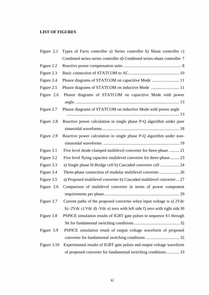
FACTS Controller is divided basically into four sub categories;
1. Series Controller injects variable voltage to the line by serial connection. As
in Figure 2.1a, it has power electronic based variable voltage source with DC
storage and inductor.
2. Shunt Controller injects variable current to line by shunt connection. As in
Figure 2.1b, it has variable source with DC storage and coupling inductor.
Aim of this study is to investigate the shunt reactive power compensation in
three-phase system.

7
3. Combined Series-Series Controller is a combination of individual series
controller that can work independently in multiline transmission system and
compensate unbalanced reactive power. It can be seen in Figure 2.1c, that
each line has a series controller using a common DC Storage.
4. Combined Series-Shunt Controller is a combination of individual series
and shunt controller. While current is injected by the shunt controller to the
line, series part injects variable voltage to the line. It has a DC storage
element and common control algorithm with coordination in Figure 2.1d
(Hingorani, 1999).
Figure 2.1 Types of Facts controller a) Series controller b) Shunt controller c) Combined series-series
controller d) Combined series-shunt controller
2.2 Shunt Connected Controller
The most popular FACTS controller is shunt type controller, which has a variable
impedance and variable source or combination of them, such as capacitors. It is

8
connected in parallel to the load and injects variable current to the system. Shunt
FACTS controller can only supply or consume reactive power because the controller
current is phase quadrature with source voltage. Thyristor Controlled Reactor (TCR),
Thyristor Switched Reactor (TSR), Thyristor Switched Capacitor (TSC) and Static
Synchronous Compensator (STATCOM) are used as Static Shunt Compensators for
variable loads.
Figure 2.2 Reactive power compensation units
2.2.1 Static VAR Compensators
Static VAR Compensator (SVC) is based on switching thyristor to compensate
reactive power by absorbing or generating it. SVC is defined in IEEE terms as “A
shunt connected static var generator or absorber whose output is adjusted to
exchange capacitive or inductive current so as to maintain or control specific
parameters (voltage level and/or power factor) of the electrical power system.”
(IEEE Terms and Definitions, 1997)
Reactive power can be compensated dynamically using TCR and TSR where anti-
parallel thyristors are connected in series with compensation inductance. The reactive
power supplied is varied by adjusting thyristor’s delay angle in TCR. In IEEE terms
and definitions TCR and TSR terms are given below.
9
Thyristor Controlled Reactor (TCR): “A shunt-connected, thyristor-controlled
inductor whose effective reactance is varied in a continuous manner by partial
conduction control of the thyristor valve.” (IEEE Terms and Definitions, 1997)
Thyristor Switched Reactor (TSR): “A shunt-connected, thyristor-switched
inductor whose effective reactance is varied in a stepwise manner by full- or zero
conduction operation of the thyristor valve.” (IEEE Terms and Definitions, 1997)
Reactive power can also be compensated by anti-parallel connected thyristors in
series with a capacitor. Compensating capacitors are switched to full or zero
conduction mode by thyristor. In IEEE terms and definitions TSC term is that
“A shunt-connected, thyristor-switched capacitor whose effective reactance is
varied in a stepwise manner by full or zero conduction operation of the thyristor
valve” (Hingorani, 1999). (IEEE Terms and Definitions, 1997)
2.2.2 Static Synchronous Compensator (STATCOM)
STATCOM is one of the essential shunt connected FACTS controller. It is
defined in IEEE definition as “A static synchronous generator operated as shunt-
connected static VAR compensator whose capacitive or inductive output current can
be controlled independent of the AC system voltage”. It may contain the voltage
source converter or current source converter. The voltage source converter is the
preferred one since it can control reactive current flow by adjusting its output
voltage. The structure of STATCOM also has the ability to work as active power
filter to cancel out current harmonics.
In IEEE definition, Static Synchronous Generator (SSG) is defined as “A static
self-commutated switching power converter supplied from an appropriate electric
energy source and operated to produce a set of adjustable multiphase output
voltages, which may be coupled to an AC power system for the purpose of
10
exchanging independently controllable real and reactive power.” (IEEE Terms and
Definitions, 1997)
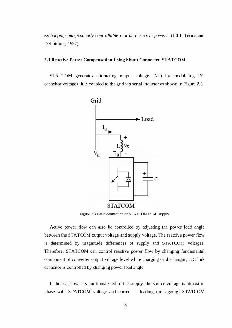
2.3 Reactive Power Compensation Using Shunt Connected STATCOM
STATCOM generates alternating output voltage (AC) by modulating DC
capacitor voltages. It is coupled to the grid via serial inductor as shown in Figure 2.3.
Figure 2.3 Basic connection of STATCOM to AC supply
Active power flow can also be controlled by adjusting the power load angle
between the STATCOM output voltage and supply voltage. The reactive power flow
is determined by magnitude differences of supply and STATCOM voltages.
Therefore, STATCOM can control reactive power flow by changing fundamental
component of converter output voltage level while charging or discharging DC link
capacitor is controlled by changing power load angle.
If the real power is not transferred to the supply, the source voltage is almost in
phase with STATCOM voltage and current is leading (or lagging) STATCOM
11
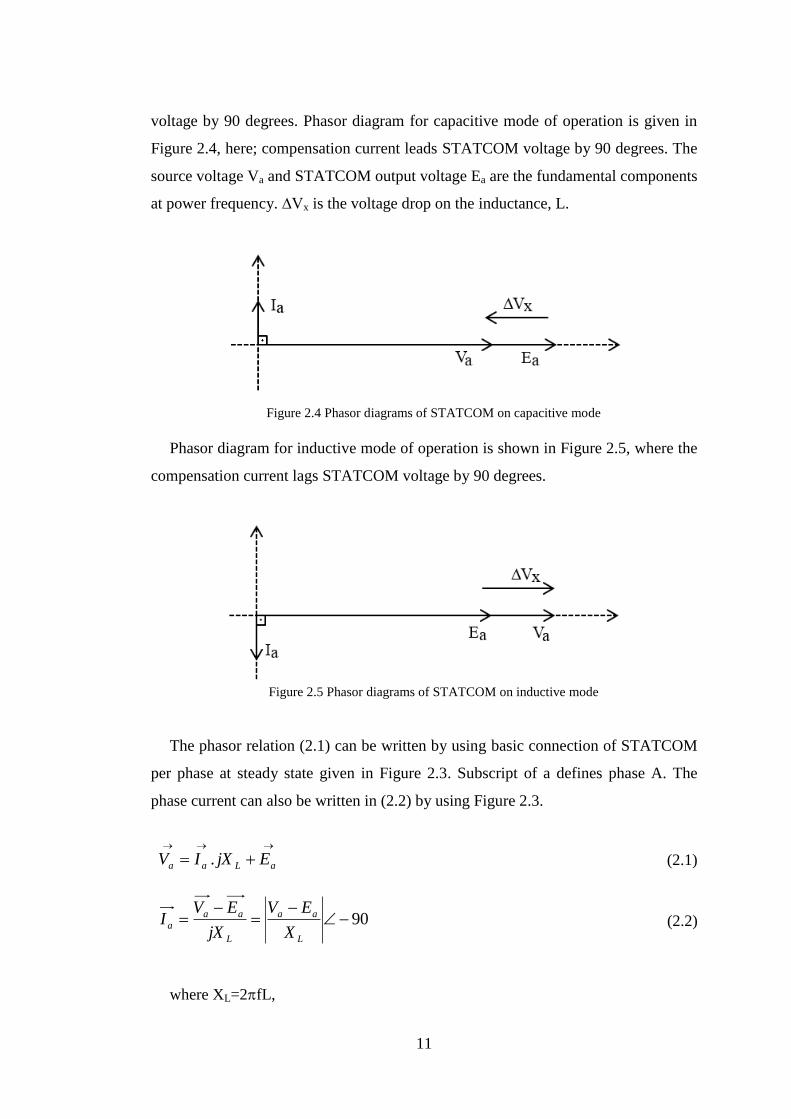
voltage by 90 degrees. Phasor diagram for capacitive mode of operation is given in
Figure 2.4, here; compensation current leads STATCOM voltage by 90 degrees. The
source voltage Va and STATCOM output voltage Ea are the fundamental components
at power frequency. ∆Vx is the voltage drop on the inductance, L.
Figure 2.4 Phasor diagrams of STATCOM on capacitive mode
Phasor diagram for inductive mode of operation is shown in Figure 2.5, where the
compensation current lags STATCOM voltage by 90 degrees.
Figure 2.5 Phasor diagrams of STATCOM on inductive mode
The phasor relation (2.1) can be written by using basic connection of STATCOM
per phase at steady state given in Figure 2.3. Subscript of a defines phase A. The
phase current can also be written in (2.2) by using Figure 2.3.
aLaa EjXIV . (2.1)
90
L
aa
L
aa
aX
EV
jX
EVI (2.2)
where XL=2fL,
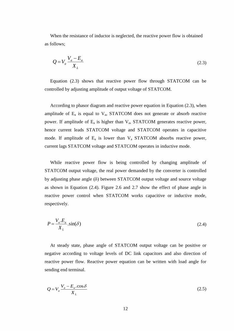
12
When the resistance of inductor is neglected, the reactive power flow is obtained
as follows;
L
aaa
X
EVVQ
(2.3)
Equation (2.3) shows that reactive power flow through STATCOM can be
controlled by adjusting amplitude of output voltage of STATCOM.
According to phasor diagram and reactive power equation in Equation (2.3), when
amplitude of Ea is equal to Va, STATCOM does not generate or absorb reactive
power. If amplitude of Ea is higher than Va, STATCOM generates reactive power,
hence current leads STATCOM voltage and STATCOM operates in capacitive
mode. If amplitude of Ea is lower than Va STATCOM absorbs reactive power,
current lags STATCOM voltage and STATCOM operates in inductive mode.
While reactive power flow is being controlled by changing amplitude of
STATCOM output voltage, the real power demanded by the converter is controlled
by adjusting phase angle () between STATCOM output voltage and source voltage
as shown in Equation (2.4). Figure 2.6 and 2.7 show the effect of phase angle in
reactive power control when STATCOM works capacitive or inductive mode,
respectively.
)sin(..
L
aa
X
EVP (2.4)
At steady state, phase angle of STATCOM output voltage can be positive or
negative according to voltage levels of DC link capacitors and also direction of
reactive power flow. Reactive power equation can be written with load angle for
sending end terminal.
L
aaa
X
EVVQ
cos. (2.5)

13
Figure 2.6 Phasor diagrams of STATCOM on capacitive mode with power angle
Figure 2.7 Phasor diagrams of STATCOM on inductive mode with power angle
14
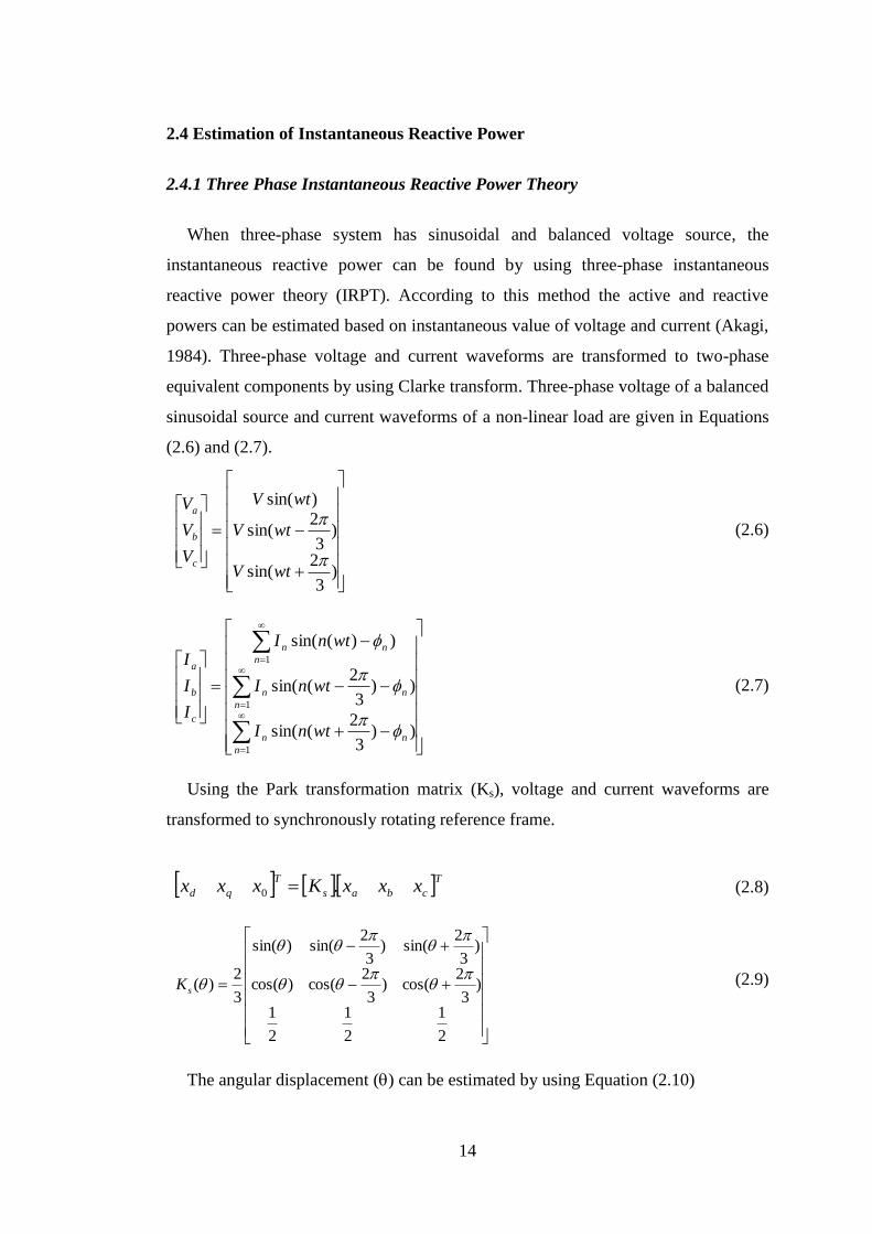
2.4 Estimation of Instantaneous Reactive Power
2.4.1 Three Phase Instantaneous Reactive Power Theory
When three-phase system has sinusoidal and balanced voltage source, the
instantaneous reactive power can be found by using three-phase instantaneous
reactive power theory (IRPT). According to this method the active and reactive
powers can be estimated based on instantaneous value of voltage and current (Akagi,
1984). Three-phase voltage and current waveforms are transformed to two-phase
equivalent components by using Clarke transform. Three-phase voltage of a balanced
sinusoidal source and current waveforms of a non-linear load are given in Equations
(2.6) and (2.7).
)3
2sin(
)3
2sin(
)sin(
wtV
wtV
wtV
V
V
V
c
b
a
(2.6)
1
1
1
))3
2(sin(
))3
2(sin(
))(sin(
n
nn
n
nn
n
nn
c
b
a
wtnI
wtnI
wtnI
I
I
I
(2.7)
Using the Park transformation matrix (Ks), voltage and current waveforms are
transformed to synchronously rotating reference frame.
Tcbas
T
qd xxxKxxx .0 (2.8)
2
1
2
1
2
1
)3
2cos()
3
2cos()cos(
)3
2sin()
3
2sin()sin(
3
2)(
sK (2.9)
The angular displacement () can be estimated by using Equation (2.10)
15
)0()(0
dw
t
(2.10)
where w is the speed of the reference frame.
After conversion of three-phase instantaneous voltages and currents to the two
axis coordinates at synchronously rotating reference frame, then the active and
reactive power equations are as follows;
)(2
3qqdddq ivivP (2.11)
)(2
3dqqddq ivivQ (2.12)
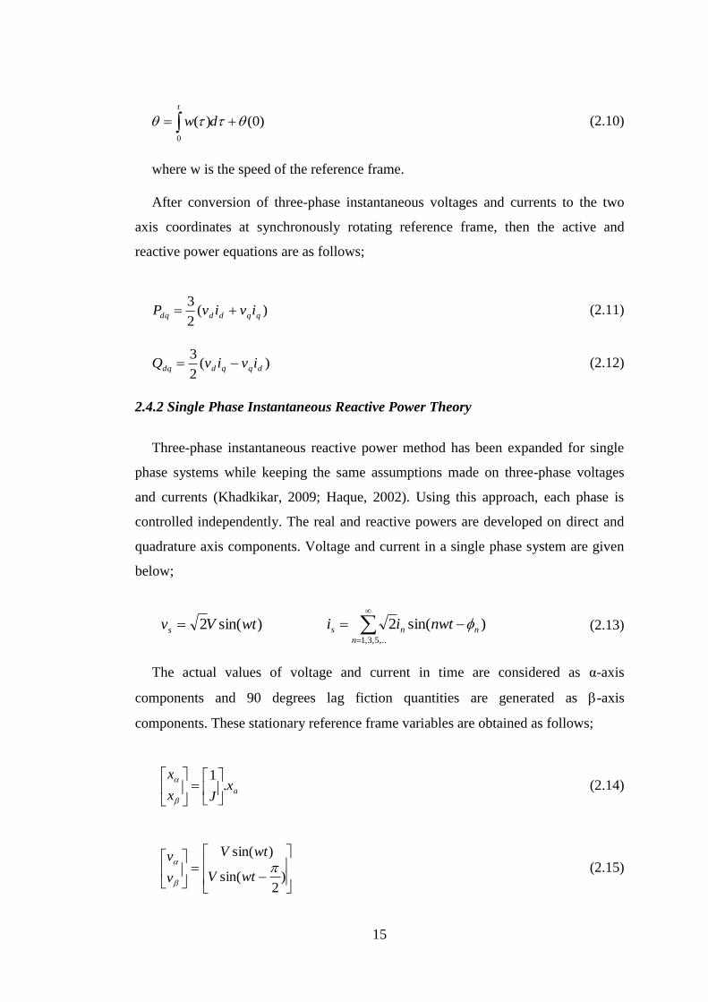
2.4.2 Single Phase Instantaneous Reactive Power Theory
Three-phase instantaneous reactive power method has been expanded for single
phase systems while keeping the same assumptions made on three-phase voltages
and currents (Khadkikar, 2009; Haque, 2002). Using this approach, each phase is
controlled independently. The real and reactive powers are developed on direct and
quadrature axis components. Voltage and current in a single phase system are given
below;
)sin(2 wtVvs
,..5,3,1
)sin(2n
nns nwtii (2.13)
The actual values of voltage and current in time are considered as α-axis
components and 90 degrees lag fiction quantities are generated as -axis
components. These stationary reference frame variables are obtained as follows;
axJx
x.
1
(2.14)
)2
sin(
)sin(
wtV
wtV
v
v (2.15)
16
..5,3,1
..5,3,1
))2
(sin(
)sin(
n
nn
n
nn
wtni
nwti
i
i
(2.16)
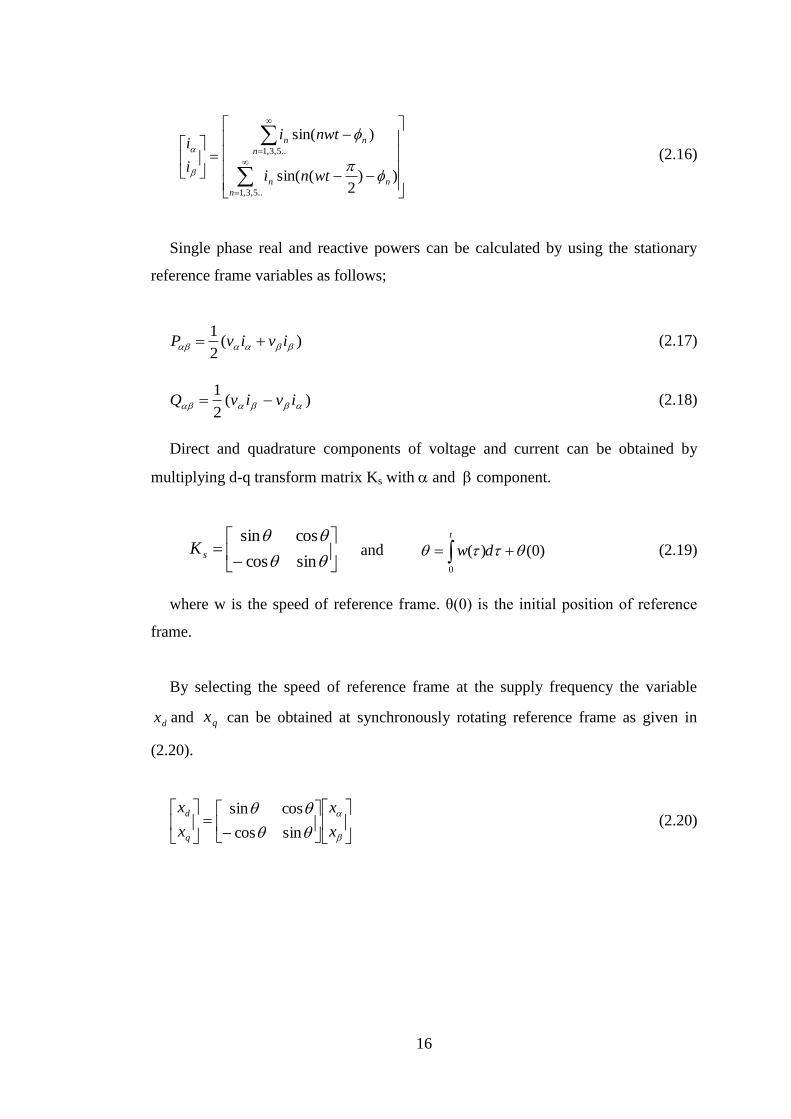
Single phase real and reactive powers can be calculated by using the stationary
reference frame variables as follows;
)(2
1 ivivP (2.17)
)(2
1 ivivQ (2.18)
Direct and quadrature components of voltage and current can be obtained by
multiplying d-q transform matrix Ks with and component.
sincos
cossinsK and )0()(
0
dw
t
(2.19)
where w is the speed of reference frame. θ(0) is the initial position of reference
frame.
By selecting the speed of reference frame at the supply frequency the variable
dx and qx can be obtained at synchronously rotating reference frame as given in
(2.20).
x
x
x
x
q
d
sincos
cossin (2.20)
17
2.5 Investigation of Single Phase P-Q with Distorted Waveform
2.5.1 Investigation of Single Phase P-Q with only Current Harmonics
The voltage is defined to include the fundamental component; current is defined
with harmonic components as Equation (2.13). The following relations can be
obtained for reactive powers using single phase P-Q method under distorted current
waves. Where, Q1 is defined as fundamental reactive power that is obtained with
multiplication of fundamental voltage and current and Q1k is defined as distortion
power that is obtained with multiplication of fundamental voltage versus harmonic
currents (2.21).
n
k
kQQQ1
11 (2.21)
Using the Equations from (2.13) to (2.20) the reactive power is calculated with
sinusoidal and non-sinusoidal currents.
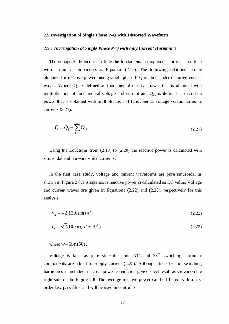
In the first case study, voltage and current waveforms are pure sinusoidal as
shown in Figure 2.8, instantaneous reactive power is calculated as DC value. Voltage
and current waves are given in Equations (2.22) and (2.23), respectively for this
analysis.
)sin(.130.2 wtva (2.22)
)30sin(.10.2 0 wtia (2.23)
where )50.(.2w ,
Voltage is kept as pure sinusoidal and 31st and 33
rd switching harmonic
components are added to supply current (2.25). Although the effect of switching
harmonics is included, reactive power calculation give correct result as shown on the
right side of the Figure 2.8. The average reactive power can be filtered with a first
order low-pass filter and will be used in controller.
18
)sin(.130.2 wtva (2.24)
))30.(33sin(.
33
1))30.(31sin(.
31
1)30sin(.10.2 000 wtwtwtia (2.25)
Figure 2.8 Reactive power calculation in Single Phase P-Q algorithm under pure sinusoidal
waveforms
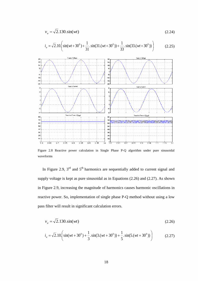
In Figure 2.9, 3rd
and 5th
harmonics are sequentially added to current signal and
supply voltage is kept as pure sinusoidal as in Equations (2.26) and (2.27). As shown
in Figure 2.9, increasing the magnitude of harmonics causes harmonic oscillations in
reactive power. So, implementation of single phase P-Q method without using a low
pass filter will result in significant calculation errors.
)sin(.130.2 wtva (2.26)
))30.(5sin(.
5
1))30.(3sin(.
3
1)30sin(.10.2 000 wtwtwtia (2.27)
19
Figure 2.9 Reactive power calculation in Single Phase P-Q algorithm under non-sinusoidal waveforms
20
CHAPTER THREE
PROPOSED MULTILEVEL CONVERTER
3.1 Introductory Remarks
The concept of multilevel inverter proposed in 1975 and applied with five level
diode-clamped multilevel converter (Nabae, 1981). In multilevel converters, output
voltage waveform approaches to sinusoidal waveform with increasing the number of
capacitor.
Cascaded multilevel converter is introduced in 1996 and the advantages and
disadvantages of this new topology are discussed (Lai, 1996). This converter is quite
ideal for high power application due to its modular design. It can be connected
medium and high voltage transmission systems without requiring a transformer with
the increasing number of output level. Besides the structure of modularity, it does not
need clamping diodes or flying capacitors like other multilevel converters.
Despite the advantage of being modular, increasing output level of cascaded
multilevel converter may lead to problems in terms of cost and size. The main
semiconductor switches and driver units bring considerable cost and space problems
in the power cabinet. Thus reducing the number of semiconductors has become a
subject of the study. The simulation results show that some proposed converters can
produce the same output voltage with conventional ones. Unfortunately, some of
them work only in inverter mode of operation (Babaei, 2008; Banaei, 2011).
The multilevel converter used in this study was presented at first in (Banaei, 2011)
with the simulation results taken from the inverter operations. In this thesis, proposed
converter has been connected to the power system and operated under bi-directional
power flow. It is investigated if the performance remains same with conventional
cascaded multilevel converters or not, while reducing the number of semiconductor
and drive units.

21
3.2 Type of Multilevel Converters as STATCOM
3.2.1 Diode-Clamped Multilevel Converter
Diode-clamped multilevel converter can produce m-level output voltage with m-1
units DC link capacitor. Bus voltage on DC link is shared with series connected
capacitors. Five level diode-clamped converter contains four DC bus capacitors for a
phase. Three-phase structure is given in Figure 3.1. Voltage stress on each capacitor
and semiconductor is limited to Vdc/4 when DC bus voltage is equal to Vdc.
Figure 3.1 Five level diode-clamped multilevel converter for three-phase
The operational logic is given in Table 3.1.
Table 3.1 Switch states of five level diode-clamped multilevel converter
Output
S1
S2
S3
S4
S1’
S2’
S3’
S4’
2Vdc 1 1 1 1 0 0 0 0
Vdc 0 1 1 1 1 0 0 0
0 0 0 1 1 1 1 0 0
-Vdc 0 0 0 1 1 1 1 0
-2Vdc 0 0 0 0 1 1 1 1

22
Advantages of diode-clamped multilevel converter against other topologies are;
All of the phases can be connected common DC link capacitors. So
the converter requires fewer capacitors (cost, weight and volume is
reduced).
The capacitors can be pre-charged.
Can be connected to a single DC source.
Disadvantages are;
Clamping diodes are subject of high voltage stress when there is more
than three output level. Clamping diodes need series connection in
order to avoid high voltage stress.
Difficult to keep in balance of DC link capacitors when there is more
than three output level.
Number of diodes grows quadratic ally according to number of output
level.
Difficulties with active power flow. (Rashid, Power Electronic
Handbook, 2006)
3.2.2 Flying-Capacitor Multilevel Converter
Flying-capacitor multilevel converter can also produce m-level output voltage
with m-1 units DC link capacitor. Capacitors in converter are connected as ladder
structure and each capacitor voltage differs from the others. In three-phase structure,
outer loop capacitors from C1 to C4 are DC link capacitors and inner loop capacitors
are balancing capacitor for each phase.
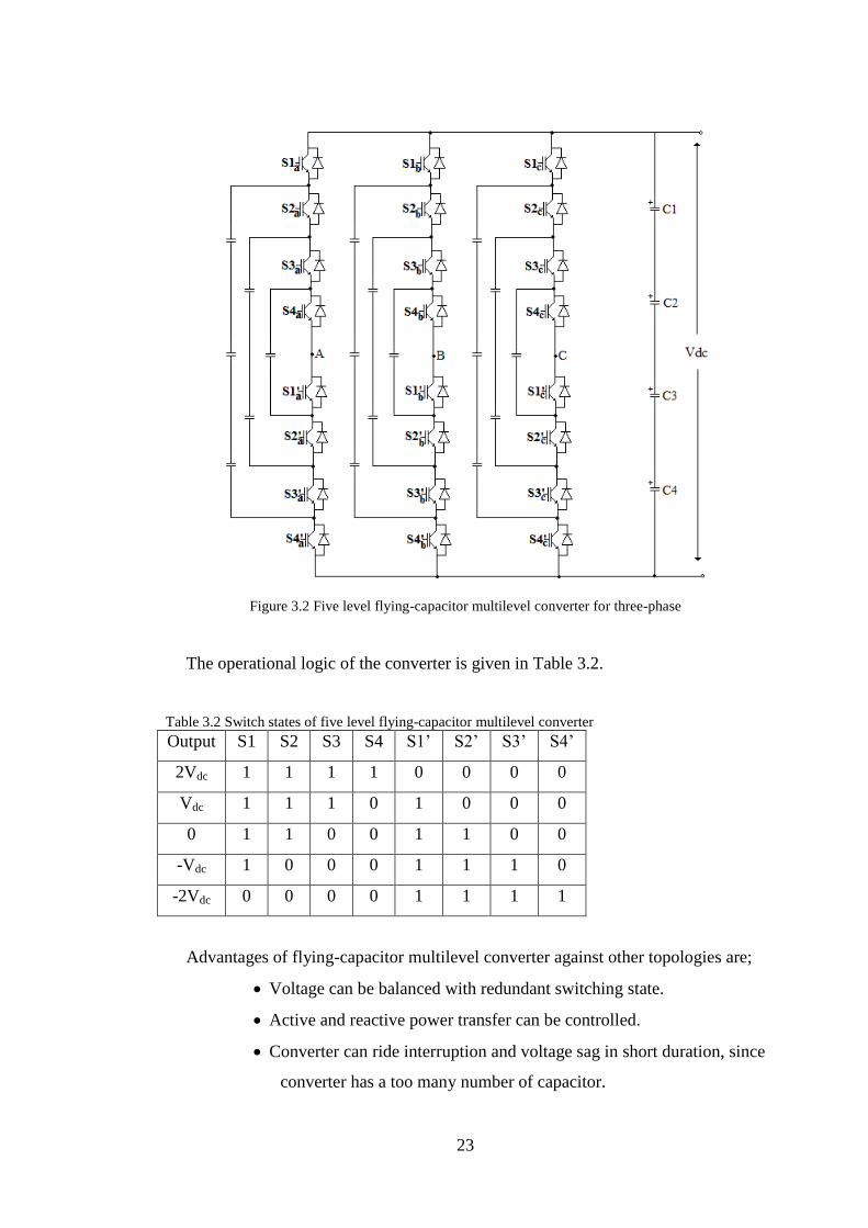
23
Figure 3.2 Five level flying-capacitor multilevel converter for three-phase
The operational logic of the converter is given in Table 3.2.
Table 3.2 Switch states of five level flying-capacitor multilevel converter
Output
S1
S2
S3
S4
S1’
S2’
S3’
S4’
2Vdc 1 1 1 1 0 0 0 0
Vdc 1 1 1 0 1 0 0 0
0 1 1 0 0 1 1 0 0
-Vdc 1 0 0 0 1 1 1 0
-2Vdc 0 0 0 0 1 1 1 1
Advantages of flying-capacitor multilevel converter against other topologies are;
Voltage can be balanced with redundant switching state.
Active and reactive power transfer can be controlled.
Converter can ride interruption and voltage sag in short duration, since
converter has a too many number of capacitor.
24
Disadvantages are;
Requires many capacitors (A large number of capacitors are bulky and
expensive than clamping diode that used in diode-clamped multilevel
converter).
Pre-charging of all the capacitor to the same DC voltage level is
complex.
Controlling of DC voltage levels for all capacitor is complicated.
(Rashid, Power Electronic Handbook, 2006)
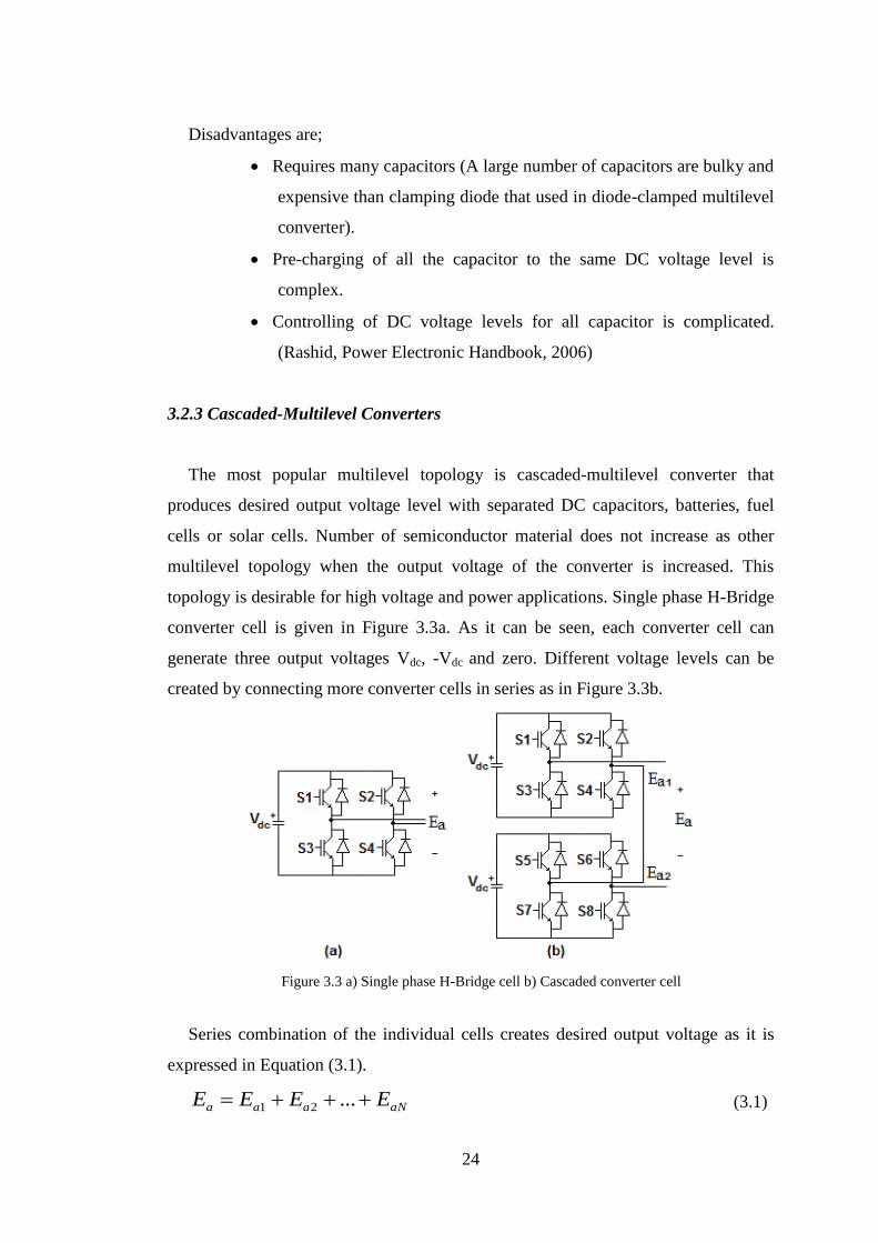
3.2.3 Cascaded-Multilevel Converters
The most popular multilevel topology is cascaded-multilevel converter that
produces desired output voltage level with separated DC capacitors, batteries, fuel
cells or solar cells. Number of semiconductor material does not increase as other
multilevel topology when the output voltage of the converter is increased. This
topology is desirable for high voltage and power applications. Single phase H-Bridge
converter cell is given in Figure 3.3a. As it can be seen, each converter cell can
generate three output voltages Vdc, -Vdc and zero. Different voltage levels can be
created by connecting more converter cells in series as in Figure 3.3b.
Figure 3.3 a) Single phase H-Bridge cell b) Cascaded converter cell
Series combination of the individual cells creates desired output voltage as it is
expressed in Equation (3.1).
aNaaa EEEE ...21 (3.1)
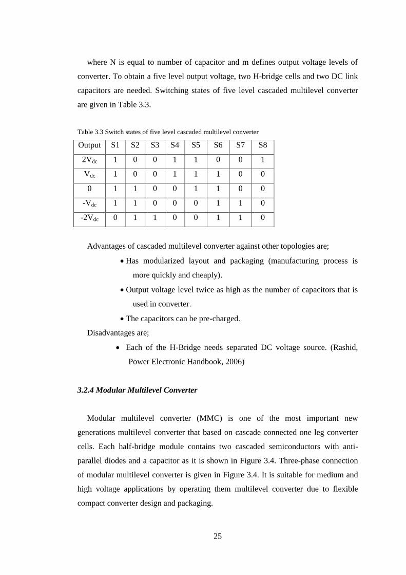
25
where N is equal to number of capacitor and m defines output voltage levels of
converter. To obtain a five level output voltage, two H-bridge cells and two DC link
capacitors are needed. Switching states of five level cascaded multilevel converter
are given in Table 3.3.
Table 3.3 Switch states of five level cascaded multilevel converter
Output
S1
S2
S3
S4
S5
S6
S7
S8
2Vdc 1 0 0 1 1 0 0 1
Vdc 1 0 0 1 1 1 0 0
0 1 1 0 0 1 1 0 0
-Vdc 1 1 0 0 0 1 1 0
-2Vdc 0 1 1 0 0 1 1 0
Advantages of cascaded multilevel converter against other topologies are;
Has modularized layout and packaging (manufacturing process is
more quickly and cheaply).
Output voltage level twice as high as the number of capacitors that is
used in converter.
The capacitors can be pre-charged.
Disadvantages are;
Each of the H-Bridge needs separated DC voltage source. (Rashid,
Power Electronic Handbook, 2006)
3.2.4 Modular Multilevel Converter
Modular multilevel converter (MMC) is one of the most important new
generations multilevel converter that based on cascade connected one leg converter
cells. Each half-bridge module contains two cascaded semiconductors with anti-
parallel diodes and a capacitor as it is shown in Figure 3.4. Three-phase connection
of modular multilevel converter is given in Figure 3.4. It is suitable for medium and
high voltage applications by operating them multilevel converter due to flexible
compact converter design and packaging.
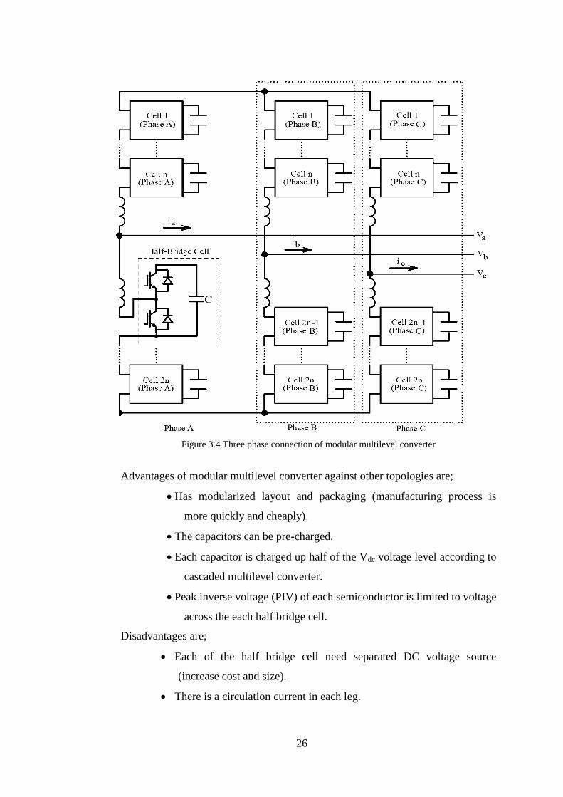
26
Figure 3.4 Three phase connection of modular multilevel converter
Advantages of modular multilevel converter against other topologies are;
Has modularized layout and packaging (manufacturing process is
more quickly and cheaply).
The capacitors can be pre-charged.
Each capacitor is charged up half of the Vdc voltage level according to
cascaded multilevel converter.
Peak inverse voltage (PIV) of each semiconductor is limited to voltage
across the each half bridge cell.
Disadvantages are;
Each of the half bridge cell need separated DC voltage source
(increase cost and size).
There is a circulation current in each leg.
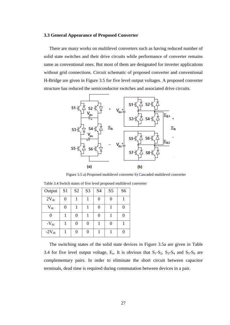
27
3.3 General Appearance of Proposed Converter
There are many works on multilevel converters such as having reduced number of
solid state switches and their drive circuits while performance of converter remains
same as conventional ones. But most of them are designated for inverter applications
without grid connections. Circuit schematic of proposed converter and conventional
H-Bridge are given in Figure 3.5 for five level output voltages. A proposed converter
structure has reduced the semiconductor switches and associated drive circuits.
Figure 3.5 a) Proposed multilevel converter b) Cascaded multilevel converter
Table 3.4 Switch states of five level proposed multilevel converter
Output
S1
S2
S3
S4
S5
S6
2Vdc 0 1 1 0 0 1
Vdc 0 1 1 0 1 0
0 1 0 1 0 1 0
-Vdc 1 0 0 1 0 1
-2Vdc 1 0 0 1 1 0
The switching states of the solid state devices in Figure 3.5a are given in Table
3.4 for five level output voltage, Ea. It is obvious that S1-S2, S3-S4 and S5-S6 are
complementary pairs. In order to eliminate the short circuit between capacitor
terminals, dead time is required during commutation between devices in a pair.
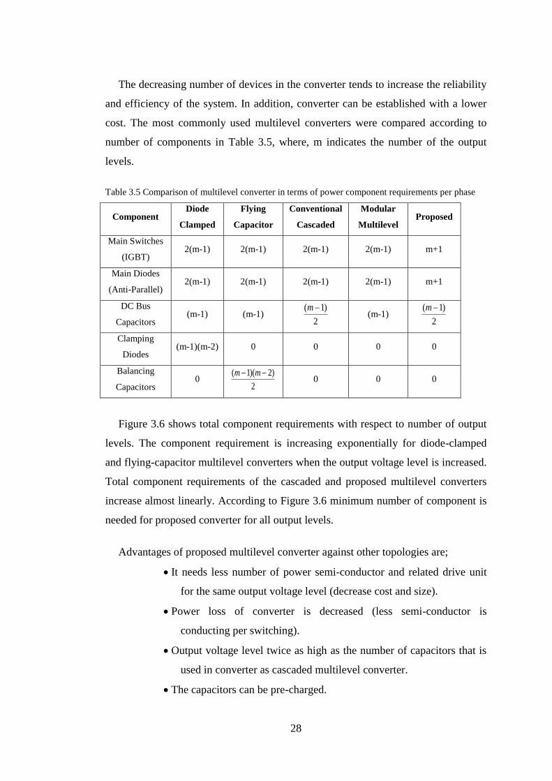
28
The decreasing number of devices in the converter tends to increase the reliability
and efficiency of the system. In addition, converter can be established with a lower
cost. The most commonly used multilevel converters were compared according to
number of components in Table 3.5, where, m indicates the number of the output
levels.
Table 3.5 Comparison of multilevel converter in terms of power component requirements per phase
Component Diode
Clamped
Flying
Capacitor
Conventional
Cascaded
Modular
Multilevel Proposed
Main Switches
(IGBT) 2(m-1) 2(m-1) 2(m-1) 2(m-1) m+1
Main Diodes
(Anti-Parallel) 2(m-1) 2(m-1) 2(m-1) 2(m-1) m+1
DC Bus
Capacitors (m-1) (m-1)
2
)1( m (m-1)
2
)1( m
Clamping
Diodes (m-1)(m-2) 0 0 0 0
Balancing
Capacitors 0
2
)2)(1( mm 0 0 0
Figure 3.6 shows total component requirements with respect to number of output
levels. The component requirement is increasing exponentially for diode-clamped
and flying-capacitor multilevel converters when the output voltage level is increased.
Total component requirements of the cascaded and proposed multilevel converters
increase almost linearly. According to Figure 3.6 minimum number of component is
needed for proposed converter for all output levels.
Advantages of proposed multilevel converter against other topologies are;
It needs less number of power semi-conductor and related drive unit
for the same output voltage level (decrease cost and size).
Power loss of converter is decreased (less semi-conductor is
conducting per switching).
Output voltage level twice as high as the number of capacitors that is
used in converter as cascaded multilevel converter.
The capacitors can be pre-charged.

29
Disadvantages are;
Each of the H-Bridge needs separated DC voltage source.
Peak inverse voltage of the semi-conductor that is located at the
middle of the converter is doubled when it is compared to other
devices in the circuit.
Figure 3.6 Comparison of multilevel converter in terms of power component requirements per phase
3.4 Switching States of Proposed Converter
The current paths and the direction of current (I) in the solid state devices during
different voltage levels are shown in Figure 3.7. There are twelve possible switching
modes for five level output voltages. When the gate pulses are applied to S2, S3 and
S6, current can flow through body diodes of S2, S3 and S6 in mode 1 or S2, S3 and
S6 in mode 2 according to direction of current flow to generate 2Vdc at the output of
STATCOM. To generate -2Vdc at the output of STATCOM, current can flow through
S1, S4 and S5 in mode 3 or body diodes of S1, S4 and S5 in mode 4. According to
direction of current flow, Vdc can be generated by mode 5 and 6; -Vdc can be

30
generated by mode 7 and 8. Other four modes (mode 9, 10, 11 and 12) show zero
levels of voltage for different switching state.
Figure 3.7 Current paths of the proposed converter when input voltage is a) 2Vdc b) -2Vdc c) Vdc d) -
Vdc e) zero with left side f) zero with right side
31
The transient analysis mode of PSPICE program computes the voltage waveforms
across the nodes defined on the circuit as a function of time by using a large signal
analysis. The non-linear characteristics of semiconductor devices are taken into
account in this approach. In the power electronic circuit proposed here, some default
values of the PSPICE program are changed without losing accuracy of the solution.
IGBT gate pulses that are used in PSPICE program are given in Figure 3.8. These
pulses are in sequence from top to bottom for the switches named S1, S2, S3, S4, S5
and S6. The stray inductance of the wiring is included into the analysis. The
inductance of 200nH is used in the path of circulating current from DC link
capacitors to IGBT module. The IGBTs part number in the implemented circuit is
SKM75GB123D by Semikron. The detailed parameters of the device related to turn-
on and turn-off behaviour have been obtained from the manufacturer data book that
is given in Appendix B. The converter output voltage over one period is obtained
from the PSPICE analysis as it is given in Figure 3.9.
When the gate pulses are applied to S1, S3 and S5 in mode 9 and mode 10, output
voltage of STATCOM decreases to zero during t1 time interval as shown in the
Figure 3.9. After turning off the gate pulses applied to these devices and turn on the
devices S2, S4 and S6 at time instant 8 msec. in Figure 3.9 a dead time of 3.5 s are
spent in order to get rid of possible short circuit across the capacitors. During this
dead time, the current circulates through the body diodes of S2, S3 and S6 and
capacitors in the network given in mode 1 and mode 2 during t2 in Figure 3.9. It is
clear that there is a voltage spike at the level of capacitor voltages (2 Vdc) between
collector and emitter of IGBT (S4) during this period and it appears on the output
voltage of converter even if the effect of stray inductance is neglected. After the dead
time, S2, S4 and S6 are activated and output voltage of STATCOM goes to zero
during t3. Experimental result of switching signals is also given in Figure 3.10.

32
Figure 3.8 PSPICE simulation results of IGBT gate pulses in sequence S1 through S6 for fundamental
switching conditions.
Figure 3.9 PSPICE simulation result of output voltage waveform of proposed converter for
fundamental switching conditions

33
Figure 3.10 Experimental results of IGBT gate pulses (S1, S2 and S3) and output voltage waveform of
proposed converter for fundamental switching conditions
3.5 Discussing on Employed Modulation Techniques for Proposed Converter
The purpose of designed STATCOM is reactive power compensation at low
voltage levels with minimum current harmonics. Reactive power compensation is
based on the control of modulation index parameter that controls the rms value of the
output voltage. Modulation techniques are generally categorized in two groups
according to switching strategies described below (Rashid, 2006).
1. Fundamental Switched Modulation: In this method, semiconductors are
switched once in a period. It is divided into two sub-categories as follows;
Selective Harmonic elimination
Space Vector Control
34
2. Pulse Width Modulation (PWM): All of the methods have high switching
frequency. It is divided into three sub-categories as follows;
Space Vector PWM
Phase Shifted PWM
Level Shifted PWM
In the thesis, selective harmonic elimination and level shifted carrier based
SPWM are implemented on proposed converter.
3.5.1 Selective Harmonic Elimination Methods
Harmonic elimination at the output voltage of multilevel converter is based on the
values of switching angle which can be estimated by using Newton-Rhapson method.
Consequently, modulation index, m defined in Equation (3.6) is also considered to
control the voltage magnitude of multilevel converter. Output voltage waveform of a
five level multilevel inverter in Figure 3.5a is depicted in Figure 3.11a. 1, 2, 3, 4,
5 and 6 indicate the instant of level change on the voltage waveform.
The square-wave voltage signals are given in Figure 3.11b through 3.11g. The
output voltage waveform is obtained by summing these voltage waveforms by using
equation below;
Vout=V1-V2+V3+V4-V5+V6 (3.2)
Equations of each voltage waveform can be written as Equation (3.3) and Fourier
series expansion of them are written as Equation (3.4).
kkdc
kkdc
kV
VV
,
2,)( (3.3)
)sin())(cos(4
)(,...5,3,1
tnnn
VtV
n
k
dc
(3.4)

35
By using the linearity property of Fourier transform which claims that if multiple
signals can be summed, their Fourier spectrums will also be summed.
According to this relationship, the Fourier series expansion of the voltage
waveform is given in Equation (3.5).
)sin())cos()cos()cos()cos()cos()(cos(4
)( 65432
,...5,3,1
1 tnnnnnnnn
VtV
n
dc
(3.5)
Let us define modulation index, m;
where s is defined as number of switching angle,
dcVs
Vm
.4.
.1 (3.6)
Figure 3.11 a) Output voltage waveform of converter b) V1 c) V2 d) V3 e) V4 f) V5 g) V6

36
The third harmonic in the line currents is automatically cancelled out for a
balanced three-phase system, if the STATCOM is delta connected as shown in
Figure 3.12. Therefore, 5th
, 7th
, 11th
, 13th
and 17th
order harmonics are eliminated to
minimize the Total Harmonic Distortion (THD) value of output voltage.
Figure 3.12 Delta-connected configuration of STATCOM
Six equations are written to solve unknown parameters 1, 2, 3, 4, 5 and 6,
simultaneously. This set of equations can be written in matrix form as follows;
Hf )( (3.7)
where 0<θ1<θ2<θ3<θ4<θ5<θ6</2
The Taylor series for a non-linear function f(θ+∆θ) is as follows;
).()()( 'fff (3.8)
High order terms are neglected.
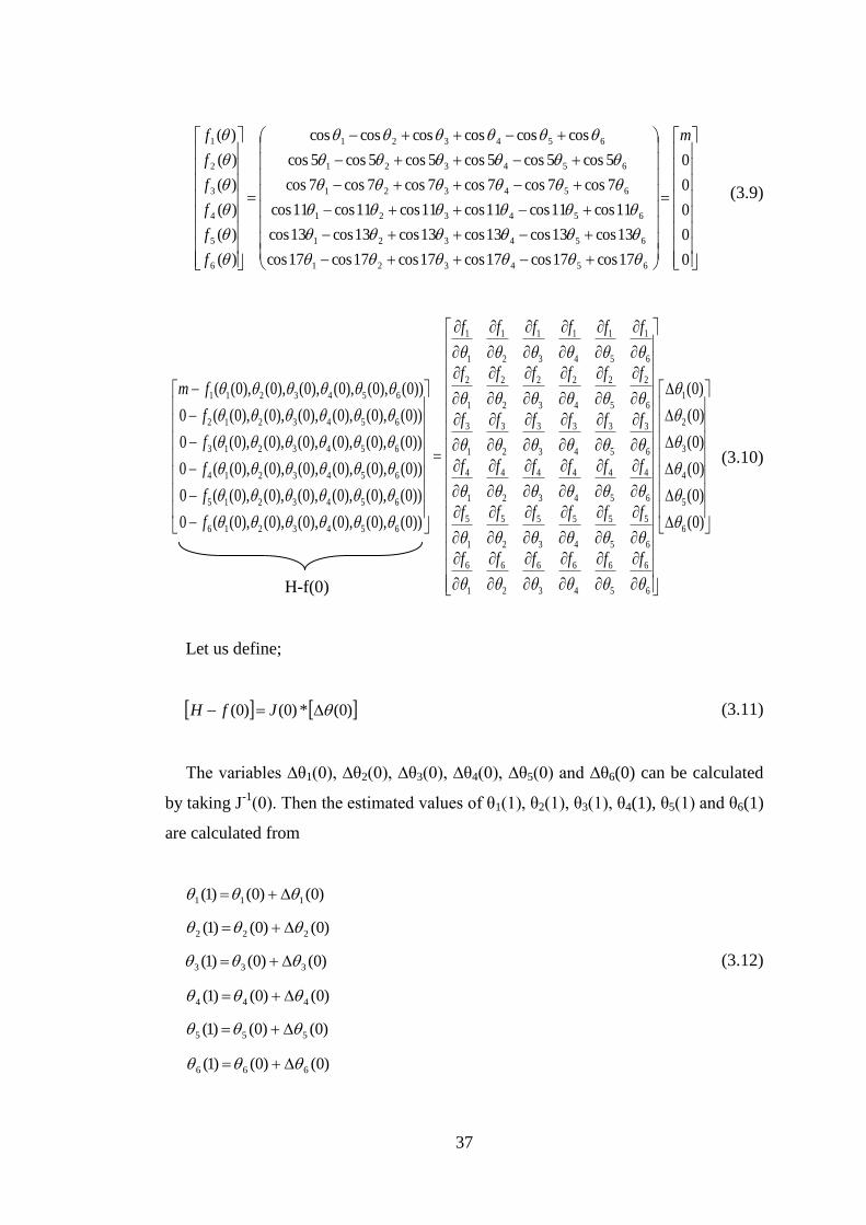
37
0
0
0
0
0
17cos17cos17cos17cos17cos17cos
13cos13cos13cos13cos13cos13cos
11cos11cos11cos11cos11cos11cos
7cos7cos7cos7cos7cos7cos
5cos5cos5cos5cos5cos5cos
coscoscoscoscoscos
)(
)(
)(
)(
)(
)(
654321
654321
654321
654321
654321
654321
6
5
4
3
2
1 m
f
f
f
f
f
f
(3.9)
)0(
)0(
)0(
)0(
)0(
)0(
))0(),0(),0(),0(),0(),0((0
))0(),0(),0(),0(),0(),0((0
))0(),0(),0(),0(),0(),0((0
))0(),0(),0(),0(),0(),0((0
))0(),0(),0(),0(),0(),0((0
))0(),0(),0(),0(),0(),0((
6
5
4
3
2
1
6
6
5
6
4
6
3
6
2
6
1
6
6
5
5
5
4
5
3
5
2
5
1
5
6
4
5
4
4
4
3
4
2
4
1
4
6
3
5
3
4
3
3
3
2
3
1
3
6
2
5
2
4
2
3
2
2
2
1
2
6
1
5
1
4
1
3
1
2
1
1
1
6543216
6543215
6543214
6543213
6543212
6543211
ffffff
ffffff
ffffff
ffffff
ffffff
ffffff
f
f
f
f
f
fm
(3.10)
Let us define;
)0(*)0()0( JfH (3.11)
The variables ∆θ1(0), ∆θ2(0), ∆θ3(0), ∆θ4(0), ∆θ5(0) and ∆θ6(0) can be calculated
by taking J-1
(0). Then the estimated values of θ1(1), θ2(1), θ3(1), θ4(1), θ5(1) and θ6(1)
are calculated from
)0()0()1( 111
)0()0()1( 222
)0()0()1( 333 (3.12)
)0()0()1( 444
)0()0()1( 555
)0()0()1( 666
H-f(0)
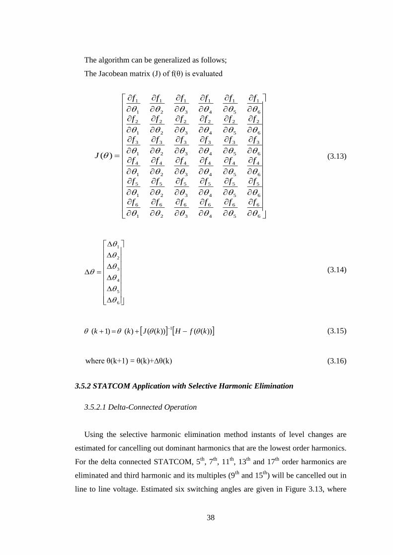
38
The algorithm can be generalized as follows;
The Jacobean matrix (J) of f(θ) is evaluated
6
6
5
6
4
6
3
6
2
6
1
6
6
5
5
5
4
5
3
5
2
5
1
5
6
4
5
4
4
4
3
4
2
4
1
4
6
3
5
3
4
3
3
3
2
3
1
3
6
2
5
2
4
2
3
2
2
2
1
2
6
1
5
1
4
1
3
1
2
1
1
1
)(
ffffff
ffffff
ffffff
ffffff
ffffff
ffffff
J (3.13)
6
5
4
3
2
1
(3.14)
))(())(()()1(1
kfHkJkk
(3.15)
where θ(k+1) = θ(k)+∆θ(k) (3.16)
3.5.2 STATCOM Application with Selective Harmonic Elimination
3.5.2.1 Delta-Connected Operation
Using the selective harmonic elimination method instants of level changes are
estimated for cancelling out dominant harmonics that are the lowest order harmonics.
For the delta connected STATCOM, 5th
, 7th
, 11th
, 13th
and 17th
order harmonics are
eliminated and third harmonic and its multiples (9th
and 15th
) will be cancelled out in
line to line voltage. Estimated six switching angles are given in Figure 3.13, where
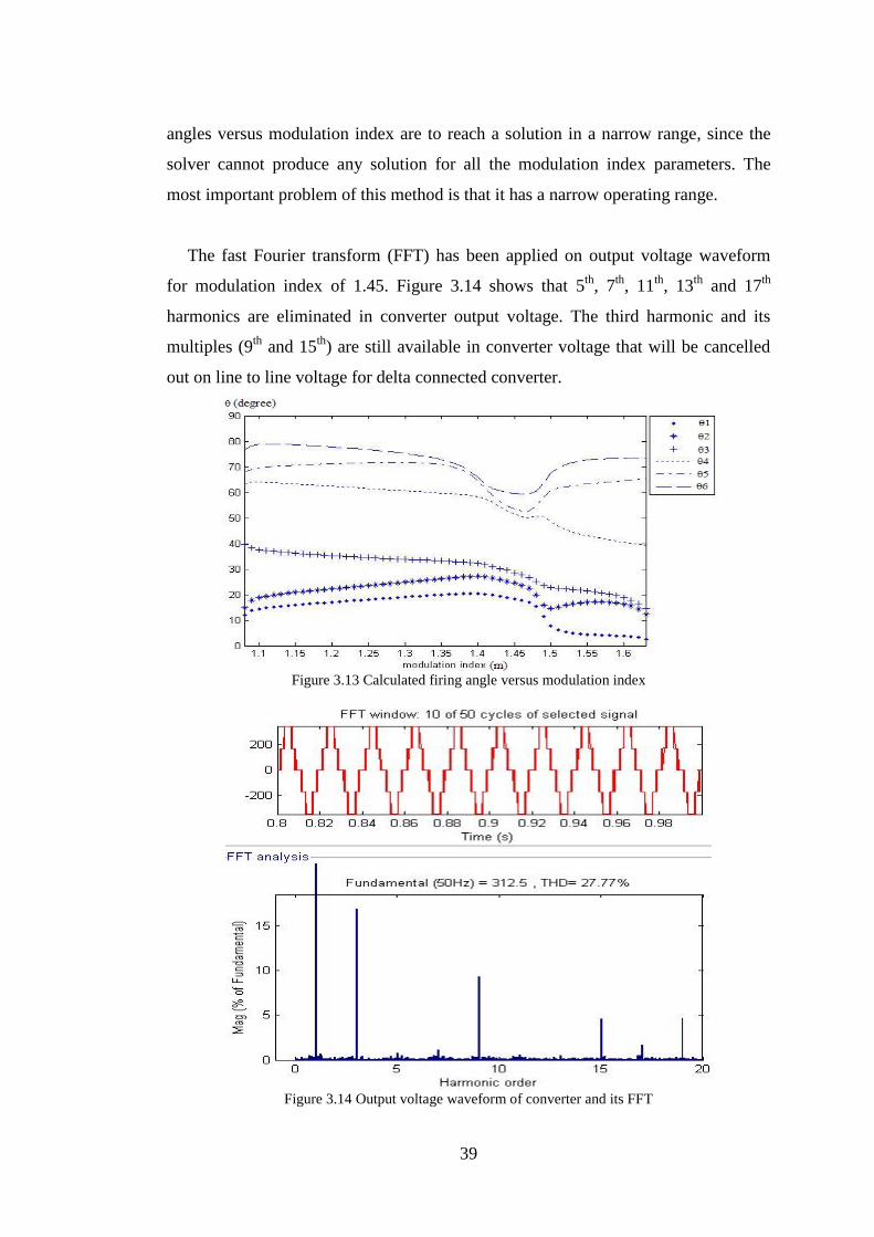
39
angles versus modulation index are to reach a solution in a narrow range, since the
solver cannot produce any solution for all the modulation index parameters. The
most important problem of this method is that it has a narrow operating range.
The fast Fourier transform (FFT) has been applied on output voltage waveform
for modulation index of 1.45. Figure 3.14 shows that 5th
, 7th
, 11th
, 13th
and 17th
harmonics are eliminated in converter output voltage. The third harmonic and its
multiples (9th
and 15th
) are still available in converter voltage that will be cancelled
out on line to line voltage for delta connected converter.
Figure 3.13 Calculated firing angle versus modulation index
Figure 3.14 Output voltage waveform of converter and its FFT
40
The general block diagram of five level delta-connected multilevel STATCOM is
given in Figure 3.15. The estimated reference reactive power is compared with actual
one; in order to generate the modulation index. When the modulation index is
known, the switching angles are obtained from look-up table that contains pre-
estimated angles. Thus, the conduction window of each semiconductor element is
obtained by adding switching angles with power angles.
Figure 3.15 Control schematic of delta-connected STATCOM
The entire system is simulated in Matlab/Simulink. The control algorithm of
STATCOM is also programmed on DSP and run in co-operation with power block in
Matlab/Simulink for testing the logic applicable. Table 3.6 shows the load
parameters.

41
Table 3.6 Loading conditions for selective harmonic elimination method using a delta-connected
STATCOM
seconds
Reactive Power (VAR) Load type Qa Qb Qc
time<1 0 0 0 No-load
1<time<2 2500 2500 2500 inductive
2<time<3 2500 2500 2500 capacitive
The results of simulation in Matlab with DSP co-operated are given in Figure
3.16. A 2.5 kVAR inductive load per phase is connected to the supply at t= 1 second.
The reactive power supplied to the load is computed as shown in Figure 3.16a. The
source current and phase voltage of STATCOM are given in Figure 3.16b. The
source current and voltage per phase are given in Figure 3.16c. It shows that current
becomes in phase with voltage after the system settles down with the response of
STATCOM. The variations of capacitor’s voltage in one phase are given in Figure
3.16d under the reference value of 300 volts.
Figure 3.16 Matlab/Simulink-DSP Co-operation result at inductive load a) Reactive power b)
STATCOM voltage & current c) Source voltage & current d) DC link voltages
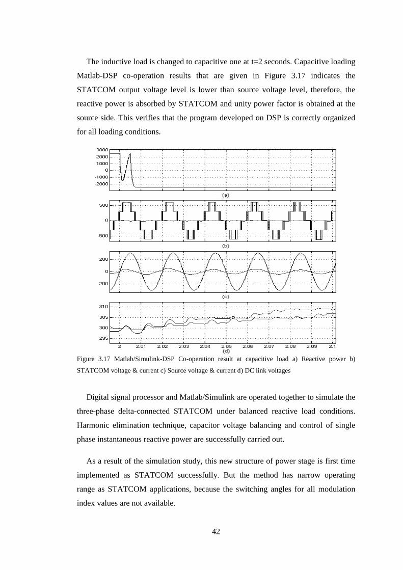
42
The inductive load is changed to capacitive one at t=2 seconds. Capacitive loading
Matlab-DSP co-operation results that are given in Figure 3.17 indicates the
STATCOM output voltage level is lower than source voltage level, therefore, the
reactive power is absorbed by STATCOM and unity power factor is obtained at the
source side. This verifies that the program developed on DSP is correctly organized
for all loading conditions.
Figure 3.17 Matlab/Simulink-DSP Co-operation result at capacitive load a) Reactive power b)
STATCOM voltage & current c) Source voltage & current d) DC link voltages
Digital signal processor and Matlab/Simulink are operated together to simulate the
three-phase delta-connected STATCOM under balanced reactive load conditions.
Harmonic elimination technique, capacitor voltage balancing and control of single
phase instantaneous reactive power are successfully carried out.
As a result of the simulation study, this new structure of power stage is first time
implemented as STATCOM successfully. But the method has narrow operating
range as STATCOM applications, because the switching angles for all modulation
index values are not available.
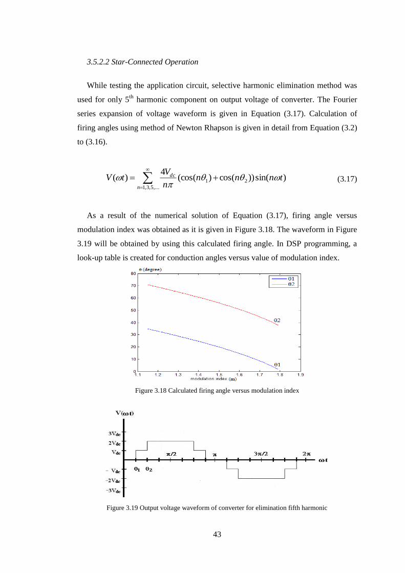
43
3.5.2.2 Star-Connected Operation
While testing the application circuit, selective harmonic elimination method was
used for only 5th
harmonic component on output voltage of converter. The Fourier
series expansion of voltage waveform is given in Equation (3.17). Calculation of
firing angles using method of Newton Rhapson is given in detail from Equation (3.2)
to (3.16).
)sin())cos()(cos(4
)( 2
,...5,3,1
1 tnnnn
VtV
n
dc
(3.17)
As a result of the numerical solution of Equation (3.17), firing angle versus
modulation index was obtained as it is given in Figure 3.18. The waveform in Figure
3.19 will be obtained by using this calculated firing angle. In DSP programming, a
look-up table is created for conduction angles versus value of modulation index.
Figure 3.18 Calculated firing angle versus modulation index
Figure 3.19 Output voltage waveform of converter for elimination fifth harmonic
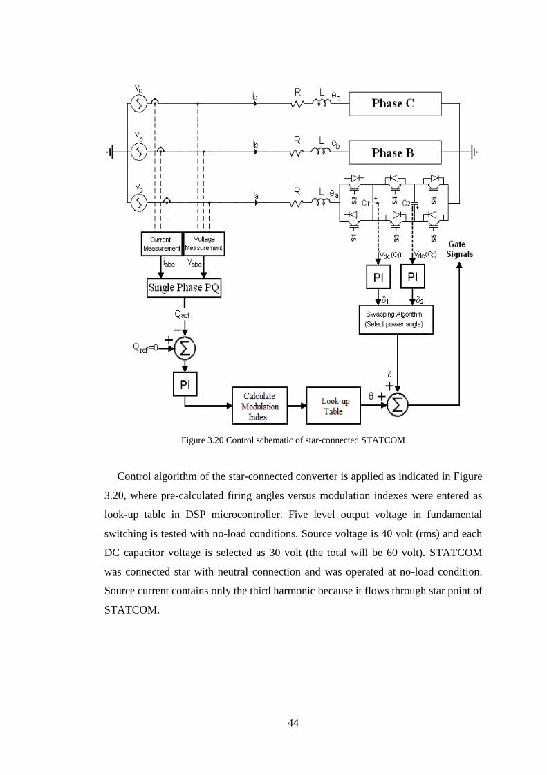
44
Figure 3.20 Control schematic of star-connected STATCOM
Control algorithm of the star-connected converter is applied as indicated in Figure
3.20, where pre-calculated firing angles versus modulation indexes were entered as
look-up table in DSP microcontroller. Five level output voltage in fundamental
switching is tested with no-load conditions. Source voltage is 40 volt (rms) and each
DC capacitor voltage is selected as 30 volt (the total will be 60 volt). STATCOM
was connected star with neutral connection and was operated at no-load condition.
Source current contains only the third harmonic because it flows through star point of
STATCOM.
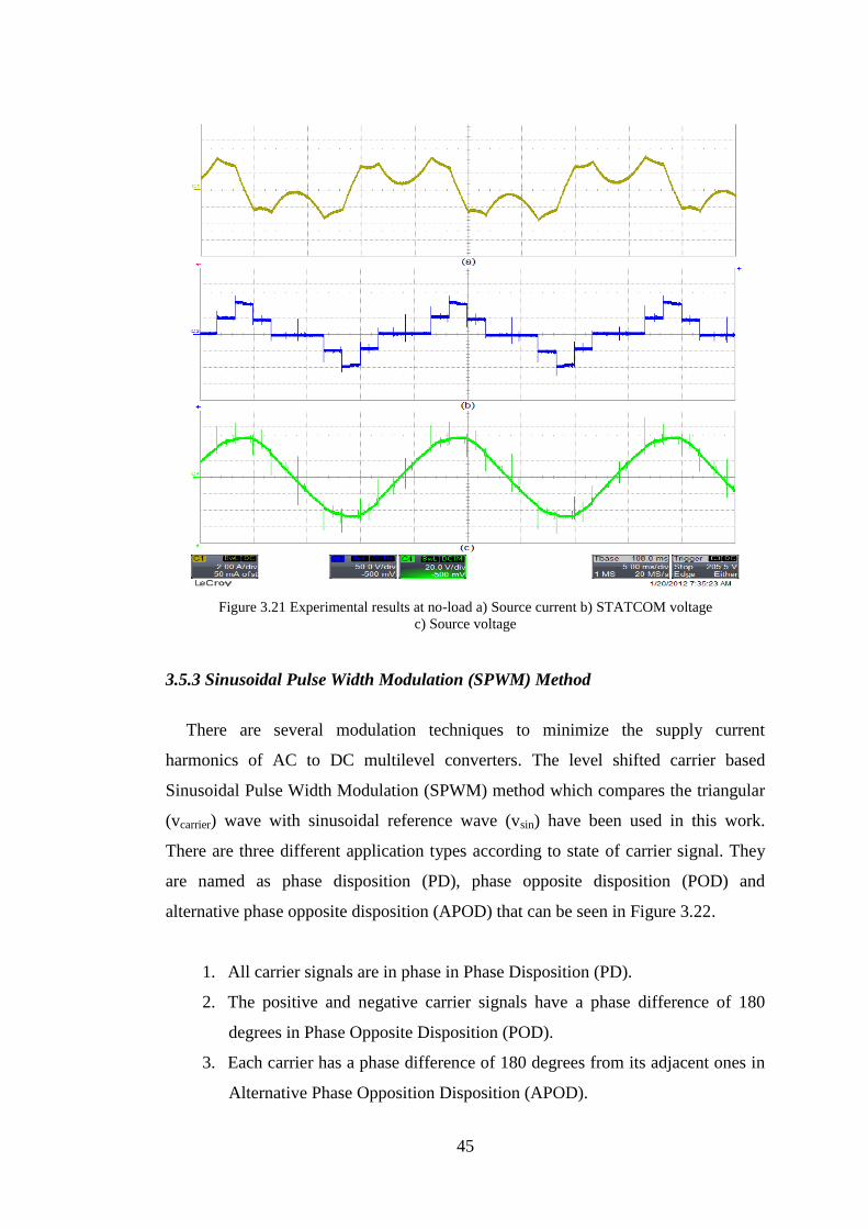
45
Figure 3.21 Experimental results at no-load a) Source current b) STATCOM voltage
c) Source voltage
3.5.3 Sinusoidal Pulse Width Modulation (SPWM) Method
There are several modulation techniques to minimize the supply current
harmonics of AC to DC multilevel converters. The level shifted carrier based
Sinusoidal Pulse Width Modulation (SPWM) method which compares the triangular
(vcarrier) wave with sinusoidal reference wave (vsin) have been used in this work.
There are three different application types according to state of carrier signal. They
are named as phase disposition (PD), phase opposite disposition (POD) and
alternative phase opposite disposition (APOD) that can be seen in Figure 3.22.
1. All carrier signals are in phase in Phase Disposition (PD).
2. The positive and negative carrier signals have a phase difference of 180
degrees in Phase Opposite Disposition (POD).
3. Each carrier has a phase difference of 180 degrees from its adjacent ones in
Alternative Phase Opposition Disposition (APOD).
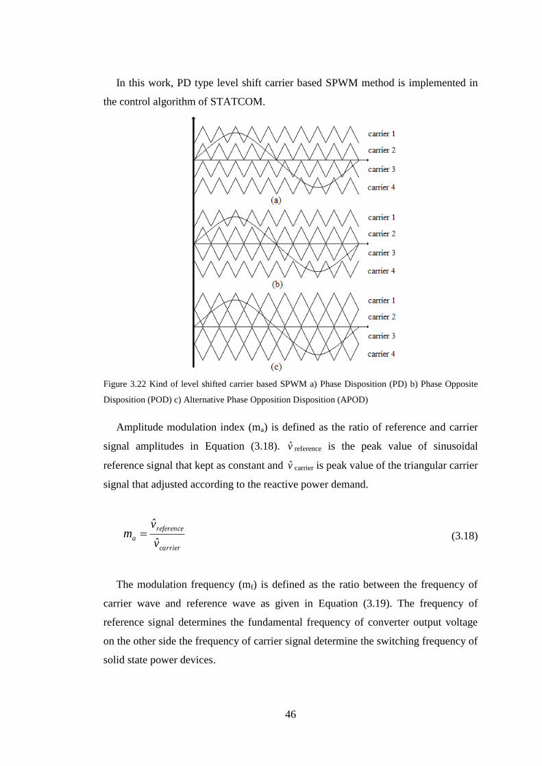
46
In this work, PD type level shift carrier based SPWM method is implemented in
the control algorithm of STATCOM.
Figure 3.22 Kind of level shifted carrier based SPWM a) Phase Disposition (PD) b) Phase Opposite
Disposition (POD) c) Alternative Phase Opposition Disposition (APOD)
Amplitude modulation index (ma) is defined as the ratio of reference and carrier
signal amplitudes in Equation (3.18). v reference is the peak value of sinusoidal
reference signal that kept as constant and v carrier is peak value of the triangular carrier
signal that adjusted according to the reactive power demand.
carrier
reference
av
vm
ˆ
ˆ (3.18)
The modulation frequency (mf) is defined as the ratio between the frequency of
carrier wave and reference wave as given in Equation (3.19). The frequency of
reference signal determines the fundamental frequency of converter output voltage
on the other side the frequency of carrier signal determine the switching frequency of
solid state power devices.
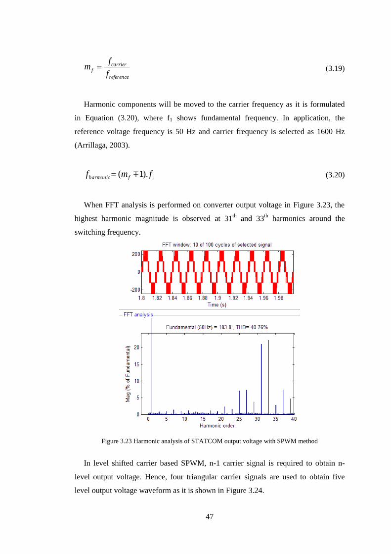
47
reference
carrierf
f
fm (3.19)
Harmonic components will be moved to the carrier frequency as it is formulated
in Equation (3.20), where f1 shows fundamental frequency. In application, the
reference voltage frequency is 50 Hz and carrier frequency is selected as 1600 Hz
(Arrillaga, 2003).
1).1( fmf fharmonic (3.20)
When FFT analysis is performed on converter output voltage in Figure 3.23, the
highest harmonic magnitude is observed at 31th
and 33th
harmonics around the
switching frequency.
Figure 3.23 Harmonic analysis of STATCOM output voltage with SPWM method
In level shifted carrier based SPWM, n-1 carrier signal is required to obtain n-
level output voltage. Hence, four triangular carrier signals are used to obtain five
level output voltage waveform as it is shown in Figure 3.24.
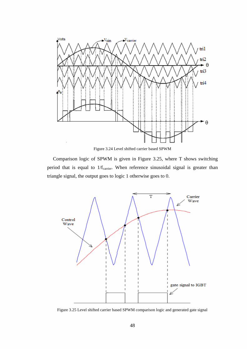
48
Figure 3.24 Level shifted carrier based SPWM
Comparison logic of SPWM is given in Figure 3.25, where T shows switching
period that is equal to 1/fcarrier. When reference sinusoidal signal is greater than
triangle signal, the output goes to logic 1 otherwise goes to 0.
Figure 3.25 Level shifted carrier based SPWM comparison logic and generated gate signal

49
In Figure 3.26, five level proposed and cascaded multilevel converter structures
are given again. The comparison logic of reference signal and triangular carrier
signal are given for cascaded multilevel converter and proposed multilevel converter
in Table 3.7 and Table 3.8, respectively. The switching states of each semiconductor
are defined for level shifted carrier based SPWM methods. In Figure 3.24, tri1, tri2,
tri3 and tri4 are shown as triangular carrier signals and Vsin is shown as sinusoidal
reference signal.
Figure 3.26 a) Proposed multilevel converter b) Cascaded multilevel converter
Table 3.7 Switch states according to reference and carrier signals for cascaded multilevel converter
S1 S2 S3 S4 S5 S6 S7 S8
Vsin > 0
Vsin < tri2
& Vsin > 0
or
Vsin > tri3
& Vsin < 0
Vsin < 0
Vsin > tri2
& Vsin > 0
or
Vsin < tri3
& Vsin < 0
Vsin < 0
Vsin < tri1
& Vsin > 0
or
Vsin > tri4
& Vsin < 0
Vsin > 0
Vsin > tri1
& Vsin > 0
or
Vsin < tri4
& Vsin < 0
Table 3.8 Switch states according to reference and carrier signals for proposed multilevel converter
S1 S2 S3 S4 S5 S6
Vsin < tri2
& Vsin > 0
or
Vsin > tri3
& Vsin < 0
Vsin > tri2
& Vsin > 0
or
Vsin < tri3
& Vsin < 0
Vsin > 0 Vsin < 0
Vsin < tri1
& Vsin > 0
or
Vsin > tri4
&Vsin < 0
Vsin > tri1
& Vsin > 0
or
Vsin < tri4
& Vsin < 0
The resulting switching states of cascaded and proposed multilevel converter are
given in Figure 3.27 and Figure 3.28, respectively. Considering the switching
signals, switching states of the proposed converter are the same as the conventional
cascaded multilevel converter.

50
Figure 3.27 Switching logic of conventional five level cascaded multilevel converter
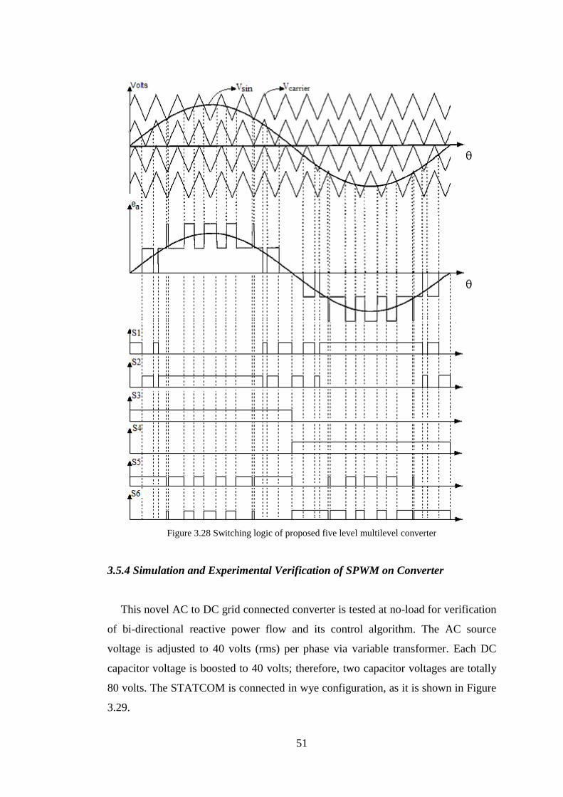
51
Figure 3.28 Switching logic of proposed five level multilevel converter
3.5.4 Simulation and Experimental Verification of SPWM on Converter
This novel AC to DC grid connected converter is tested at no-load for verification
of bi-directional reactive power flow and its control algorithm. The AC source
voltage is adjusted to 40 volts (rms) per phase via variable transformer. Each DC
capacitor voltage is boosted to 40 volts; therefore, two capacitor voltages are totally
80 volts. The STATCOM is connected in wye configuration, as it is shown in Figure
3.29.
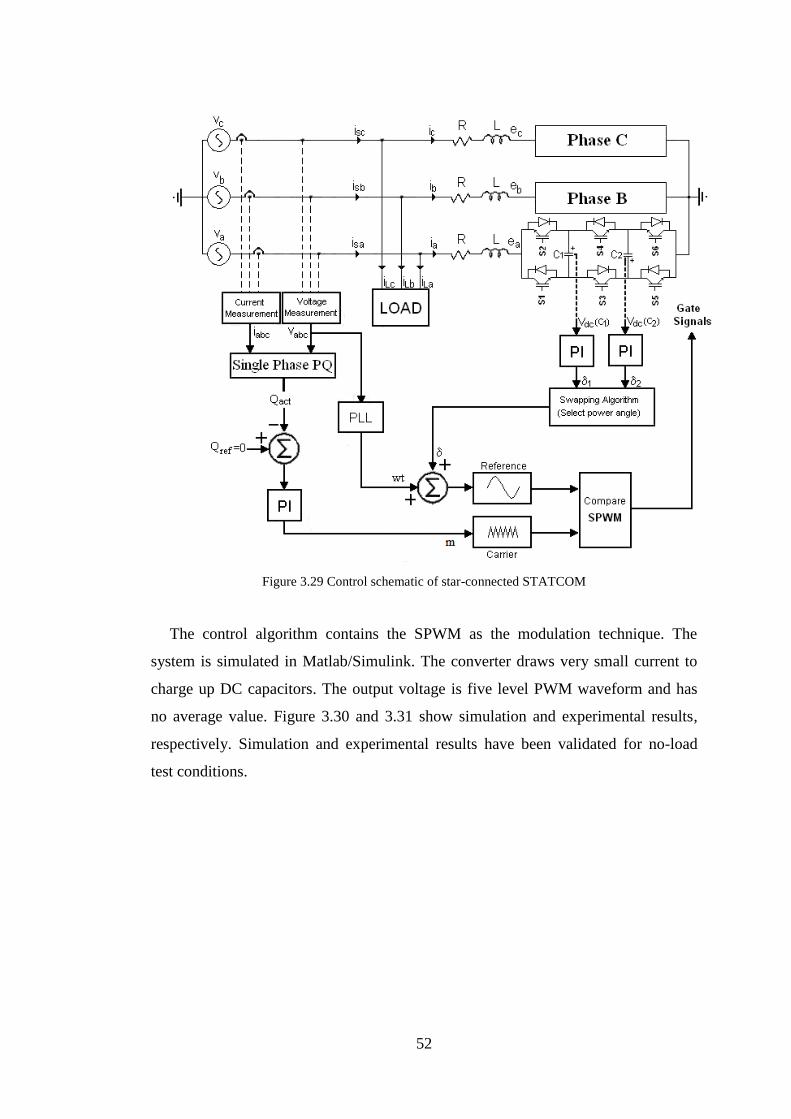
52
Figure 3.29 Control schematic of star-connected STATCOM
The control algorithm contains the SPWM as the modulation technique. The
system is simulated in Matlab/Simulink. The converter draws very small current to
charge up DC capacitors. The output voltage is five level PWM waveform and has
no average value. Figure 3.30 and 3.31 show simulation and experimental results,
respectively. Simulation and experimental results have been validated for no-load
test conditions.
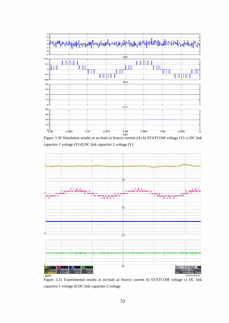
53
Figure 3.30 Simulation results at no-load a) Source current (A) b) STATCOM voltage (V) c) DC link
capacitor 1 voltage (V) d) DC link capacitor 2 voltage (V)
Figure 3.31 Experimental results at no-load a) Source current b) STATCOM voltage c) DC link
capacitor 1 voltage d) DC link capacitor 2 voltage
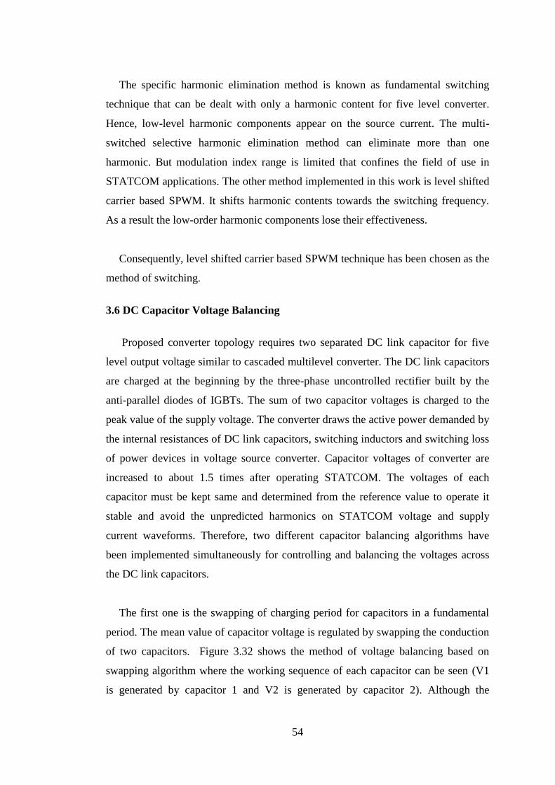
54
The specific harmonic elimination method is known as fundamental switching
technique that can be dealt with only a harmonic content for five level converter.
Hence, low-level harmonic components appear on the source current. The multi-
switched selective harmonic elimination method can eliminate more than one
harmonic. But modulation index range is limited that confines the field of use in
STATCOM applications. The other method implemented in this work is level shifted
carrier based SPWM. It shifts harmonic contents towards the switching frequency.
As a result the low-order harmonic components lose their effectiveness.
Consequently, level shifted carrier based SPWM technique has been chosen as the
method of switching.
3.6 DC Capacitor Voltage Balancing
Proposed converter topology requires two separated DC link capacitor for five
level output voltage similar to cascaded multilevel converter. The DC link capacitors
are charged at the beginning by the three-phase uncontrolled rectifier built by the
anti-parallel diodes of IGBTs. The sum of two capacitor voltages is charged to the
peak value of the supply voltage. The converter draws the active power demanded by
the internal resistances of DC link capacitors, switching inductors and switching loss
of power devices in voltage source converter. Capacitor voltages of converter are
increased to about 1.5 times after operating STATCOM. The voltages of each
capacitor must be kept same and determined from the reference value to operate it
stable and avoid the unpredicted harmonics on STATCOM voltage and supply
current waveforms. Therefore, two different capacitor balancing algorithms have
been implemented simultaneously for controlling and balancing the voltages across
the DC link capacitors.
The first one is the swapping of charging period for capacitors in a fundamental
period. The mean value of capacitor voltage is regulated by swapping the conduction
of two capacitors. Figure 3.32 shows the method of voltage balancing based on
swapping algorithm where the working sequence of each capacitor can be seen (V1
is generated by capacitor 1 and V2 is generated by capacitor 2). Although the
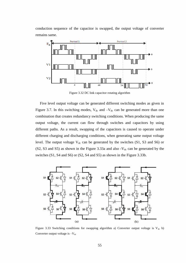
55
conduction sequence of the capacitor is swapped, the output voltage of converter
remains same.
Figure 3.32 DC link capacitor rotating algorithm
Five level output voltage can be generated different switching modes as given in
Figure 3.7. In this switching modes, Vdc and –Vdc can be generated more than one
combination that creates redundancy switching conditions. When producing the same
output voltage, the current can flow through switches and capacitors by using
different paths. As a result, swapping of the capacitors is caused to operate under
different charging and discharging conditions, when generating same output voltage
level. The output voltage Vdc can be generated by the switches (S1, S3 and S6) or
(S2, S3 and S5) as shown in the Figure 3.33a and also -Vdc can be generated by the
switches (S1, S4 and S6) or (S2, S4 and S5) as shown in the Figure 3.33b.
Figure 3.33 Switching conditions for swapping algorithm a) Converter output voltage is Vdc b)
Converter output voltage is –Vdc
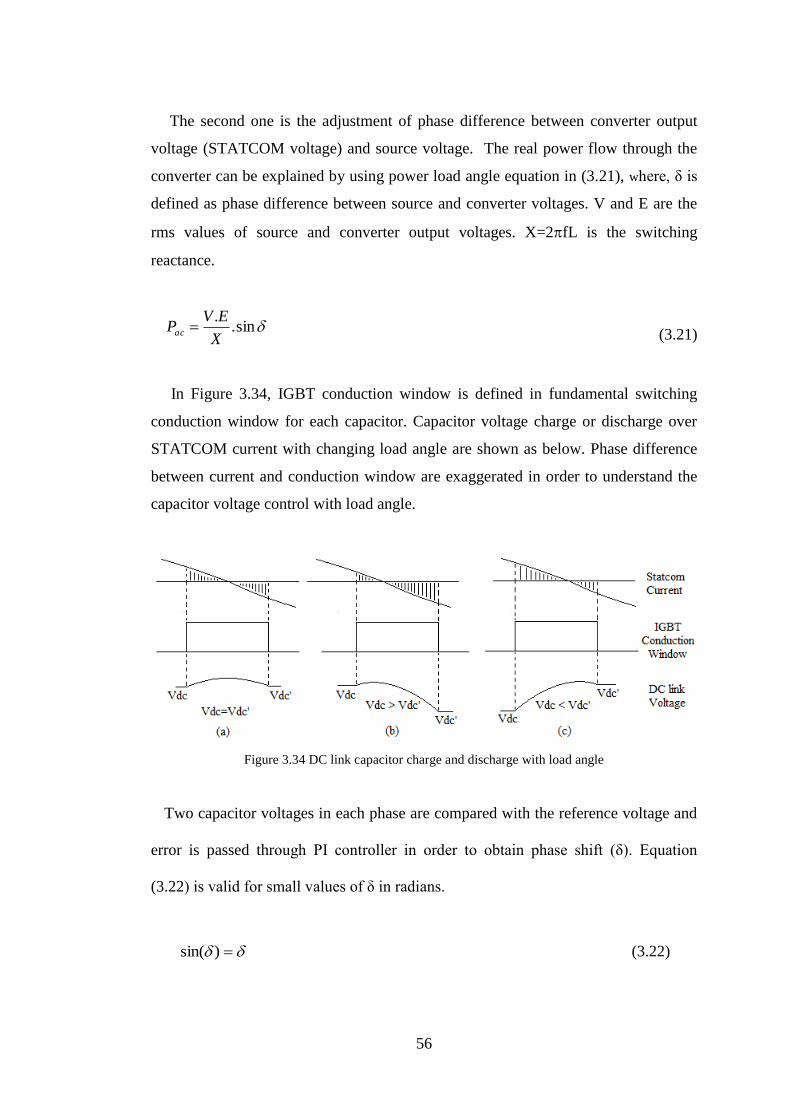
56
The second one is the adjustment of phase difference between converter output
voltage (STATCOM voltage) and source voltage. The real power flow through the
converter can be explained by using power load angle equation in (3.21), where, δ is
defined as phase difference between source and converter voltages. V and E are the
rms values of source and converter output voltages. X=2fL is the switching
reactance.
sin..
X
EVPac (3.21)
In Figure 3.34, IGBT conduction window is defined in fundamental switching
conduction window for each capacitor. Capacitor voltage charge or discharge over
STATCOM current with changing load angle are shown as below. Phase difference
between current and conduction window are exaggerated in order to understand the
capacitor voltage control with load angle.
Figure 3.34 DC link capacitor charge and discharge with load angle
Two capacitor voltages in each phase are compared with the reference voltage and
error is passed through PI controller in order to obtain phase shift (δ). Equation
(3.22) is valid for small values of δ in radians.
)sin( (3.22)
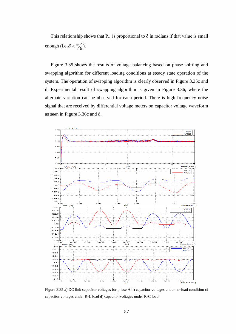
57
This relationship shows that Pac is proportional to δ in radians if that value is small
enough (i.e,6
).
Figure 3.35 shows the results of voltage balancing based on phase shifting and
swapping algorithm for different loading conditions at steady state operation of the
system. The operation of swapping algorithm is clearly observed in Figure 3.35c and
d. Experimental result of swapping algorithm is given in Figure 3.36, where the
alternate variation can be observed for each period. There is high frequency noise
signal that are received by differential voltage meters on capacitor voltage waveform
as seen in Figure 3.36c and d.
Figure 3.35 a) DC link capacitor voltages for phase A b) capacitor voltages under no-load condition c)
capacitor voltages under R-L load d) capacitor voltages under R-C load
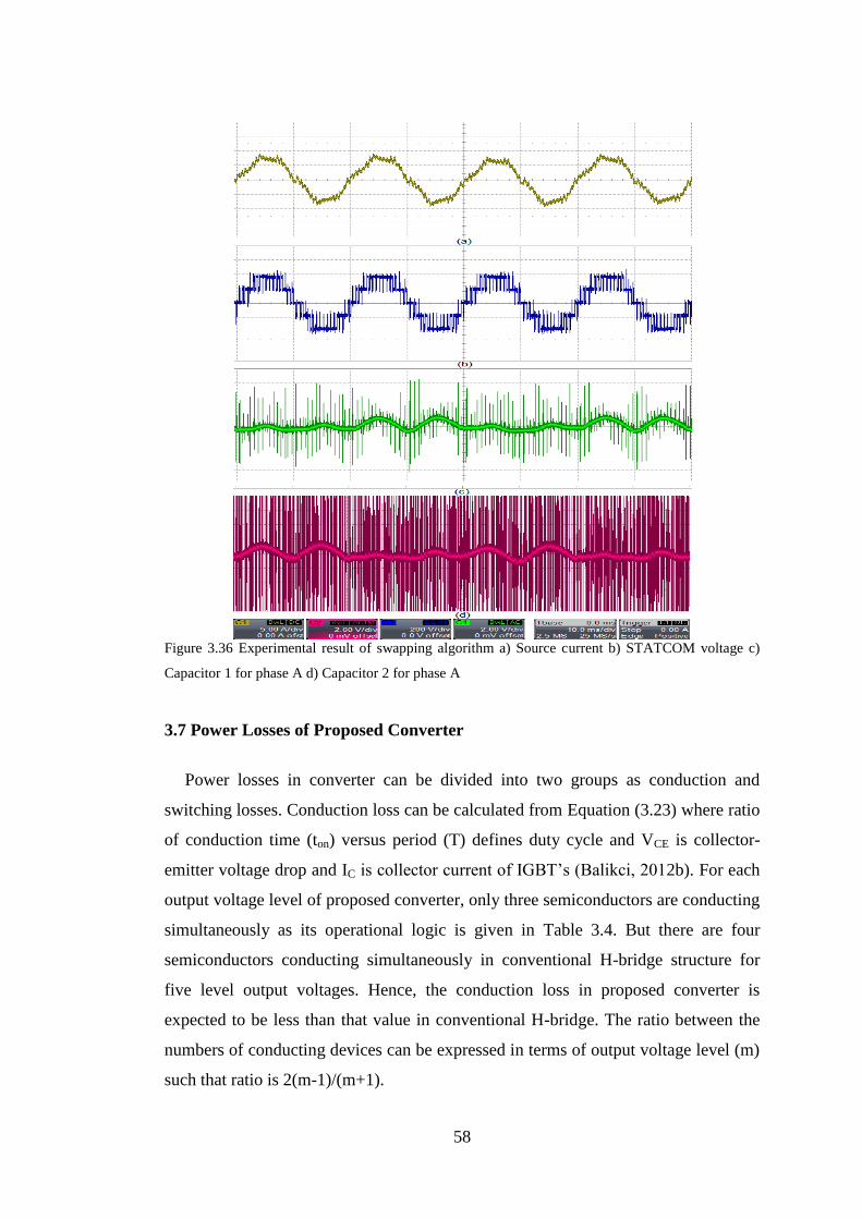
58
Figure 3.36 Experimental result of swapping algorithm a) Source current b) STATCOM voltage c)
Capacitor 1 for phase A d) Capacitor 2 for phase A
3.7 Power Losses of Proposed Converter
Power losses in converter can be divided into two groups as conduction and
switching losses. Conduction loss can be calculated from Equation (3.23) where ratio
of conduction time (ton) versus period (T) defines duty cycle and VCE is collector-
emitter voltage drop and IC is collector current of IGBT’s (Balikci, 2012b). For each
output voltage level of proposed converter, only three semiconductors are conducting
simultaneously as its operational logic is given in Table 3.4. But there are four
semiconductors conducting simultaneously in conventional H-bridge structure for
five level output voltages. Hence, the conduction loss in proposed converter is
expected to be less than that value in conventional H-bridge. The ratio between the
numbers of conducting devices can be expressed in terms of output voltage level (m)
such that ratio is 2(m-1)/(m+1).
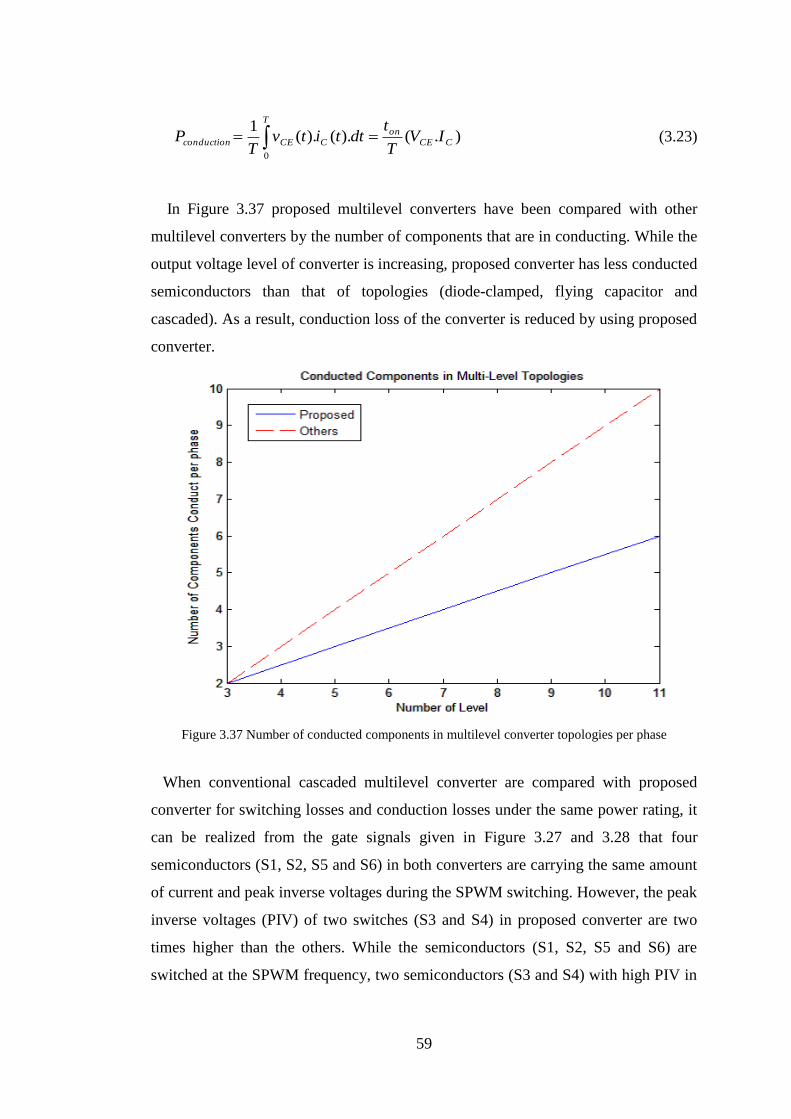
59
).().().(1
0
CCE
on
T
CCEconduction IVT
tdttitv
TP (3.23)
In Figure 3.37 proposed multilevel converters have been compared with other
multilevel converters by the number of components that are in conducting. While the
output voltage level of converter is increasing, proposed converter has less conducted
semiconductors than that of topologies (diode-clamped, flying capacitor and
cascaded). As a result, conduction loss of the converter is reduced by using proposed
converter.
Figure 3.37 Number of conducted components in multilevel converter topologies per phase
When conventional cascaded multilevel converter are compared with proposed
converter for switching losses and conduction losses under the same power rating, it
can be realized from the gate signals given in Figure 3.27 and 3.28 that four
semiconductors (S1, S2, S5 and S6) in both converters are carrying the same amount
of current and peak inverse voltages during the SPWM switching. However, the peak
inverse voltages (PIV) of two switches (S3 and S4) in proposed converter are two
times higher than the others. While the semiconductors (S1, S2, S5 and S6) are
switched at the SPWM frequency, two semiconductors (S3 and S4) with high PIV in
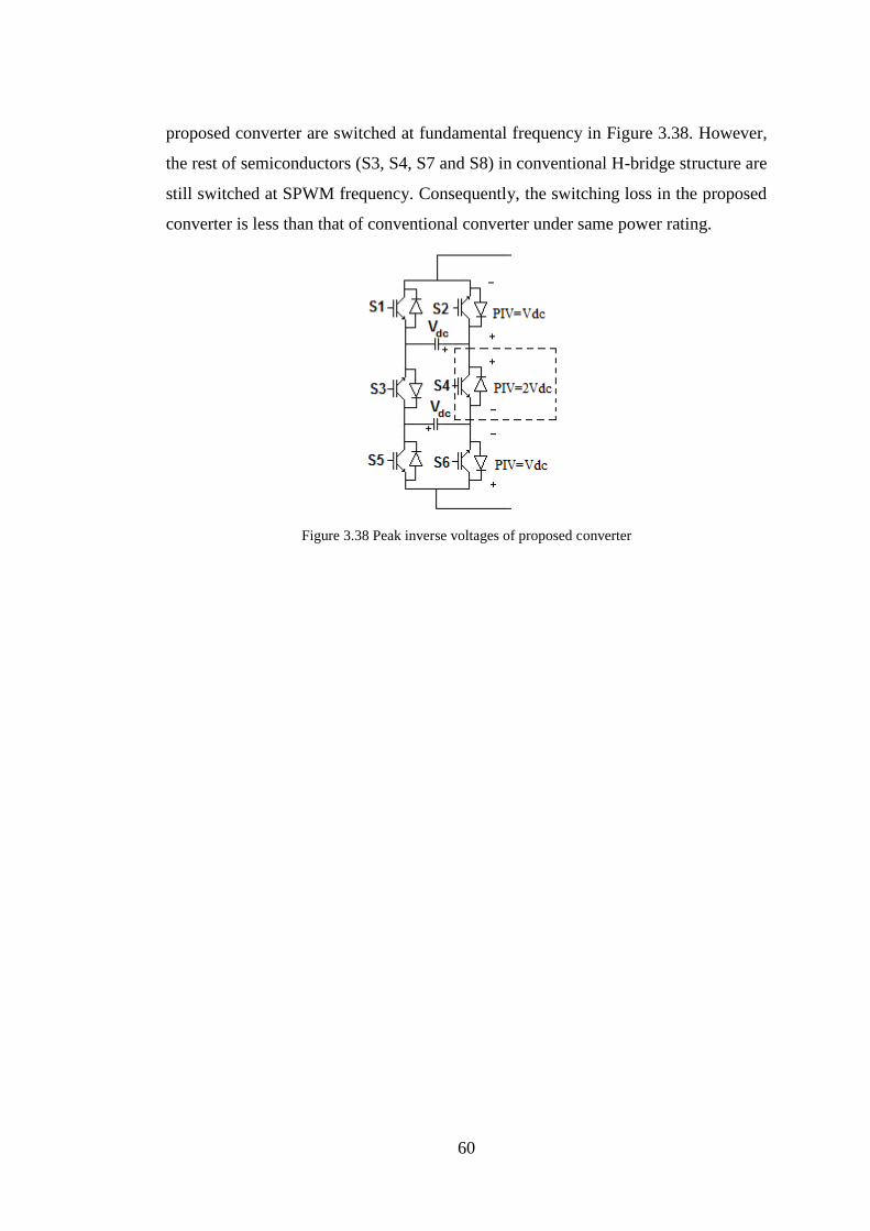
60
proposed converter are switched at fundamental frequency in Figure 3.38. However,
the rest of semiconductors (S3, S4, S7 and S8) in conventional H-bridge structure are
still switched at SPWM frequency. Consequently, the switching loss in the proposed
converter is less than that of conventional converter under same power rating.
Figure 3.38 Peak inverse voltages of proposed converter
61
CHAPTER FOUR
DESIGN OF THREE PHASE MULTILEVEL STATCOM
4.1 Introductory Remarks
In literature, DSP based three-phase STATCOM applications are presented. In
past the DSP is used for firing angle control, digital Phase Locked Loop (PLL),
digital Proportional Integral (PI) controller and reactive power estimation (Singh,
2000). Usage of conventional six-pulse voltage source converter, sinusoidal pulse
width modulation are applied with DSP that control reactive power flow,
synchronization with supply and DC link balancing (Xu., 2001). A distribution Static
VAR Compensator is controlled with DSP and its detailed circuit schematics were
given in (Mishra, 2006). A transmission static synchronous compensator is
implemented for reactive power compensation and power system stability. A master
DSP and slave DSP in a single application were used for system controller and a
FPGA was used for auxiliary operations (Gultekin, 2012).
In this chapter, hardware and software design for STATCOM are presented.
Implementation problems encountered and their solutions are included. Circuit
schematics and photography of the final version of the each hardware, switching
topology of the proposed converter are also given. A detailed flow chart of the
program code and execution times of each task are also presented.
4.2 Hardware Design
4.2.1 Design of Main Control Cards
Hardware of power converter is designed with SEMIKRON SKM75GB123D
IGBT modules. Technical specifications of dual pack IGBT modules are given in
Table 4.1 for 25 0C ambient temperature. While picture of semiconductor shows
power and driver connection pins for IGBT in Figure 4.1a, circuit diagram of dual
pack modules are given in Figure 4.1b. IGBT modules are driven with SEMIKRON
SKYPER 32 PRO R dual pack IGBT driver modules that have short circuit, over-
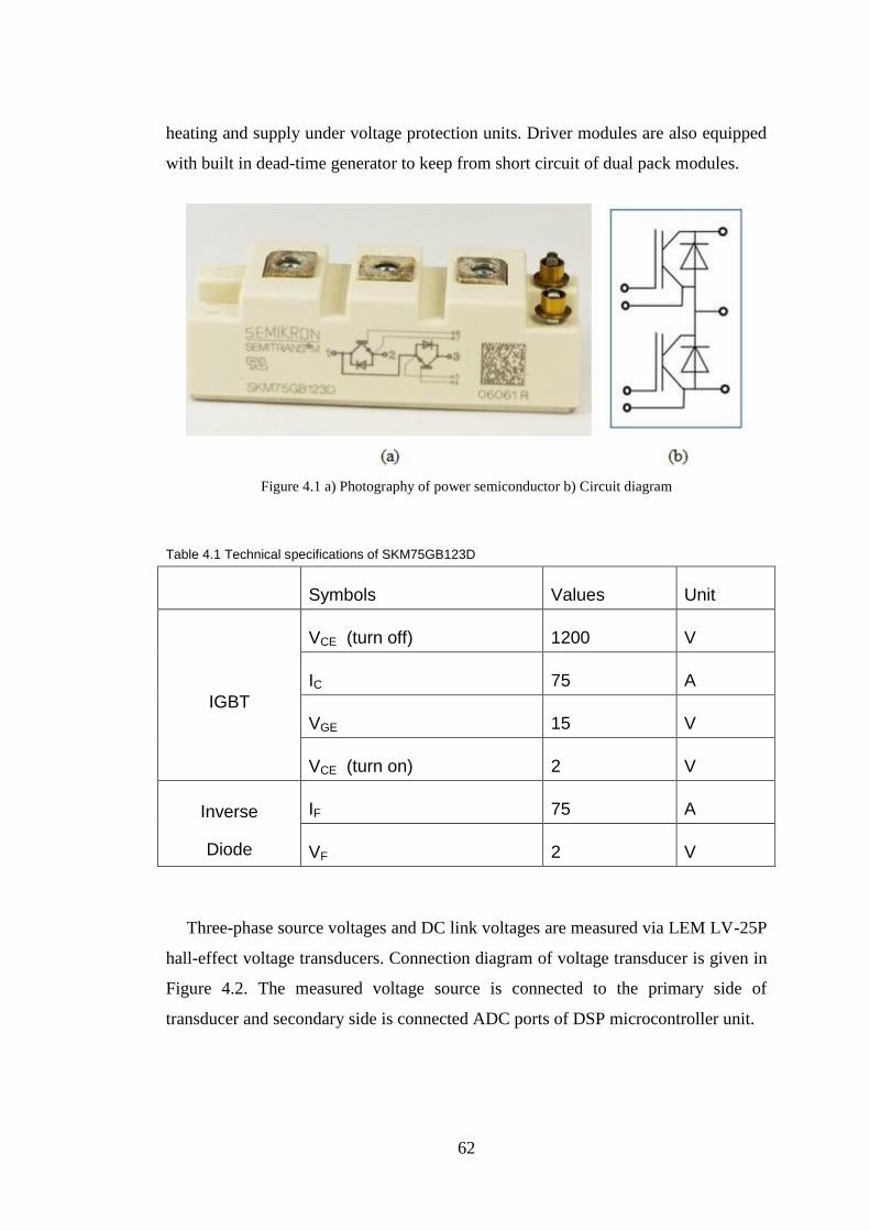
62
heating and supply under voltage protection units. Driver modules are also equipped
with built in dead-time generator to keep from short circuit of dual pack modules.
Figure 4.1 a) Photography of power semiconductor b) Circuit diagram
Table 4.1 Technical specifications of SKM75GB123D
Symbols Values Unit
IGBT
VCE (turn off) 1200 V
IC 75 A
VGE 15 V
VCE (turn on) 2 V
Inverse
Diode
IF 75 A
VF 2 V
Three-phase source voltages and DC link voltages are measured via LEM LV-25P
hall-effect voltage transducers. Connection diagram of voltage transducer is given in
Figure 4.2. The measured voltage source is connected to the primary side of
transducer and secondary side is connected ADC ports of DSP microcontroller unit.
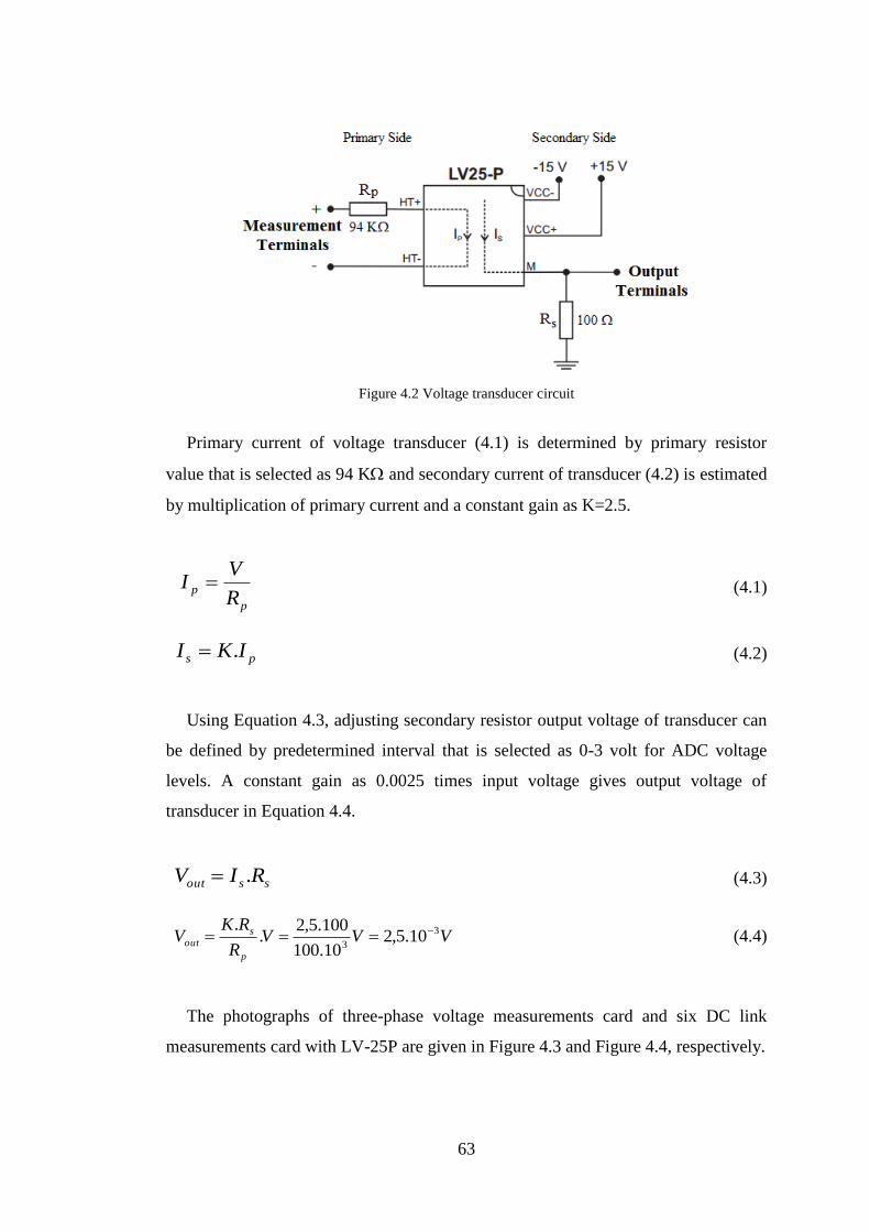
63
Figure 4.2 Voltage transducer circuit
Primary current of voltage transducer (4.1) is determined by primary resistor
value that is selected as 94 K and secondary current of transducer (4.2) is estimated
by multiplication of primary current and a constant gain as K=2.5.
p
pR
VI (4.1)
ps IKI . (4.2)
Using Equation 4.3, adjusting secondary resistor output voltage of transducer can
be defined by predetermined interval that is selected as 0-3 volt for ADC voltage
levels. A constant gain as 0.0025 times input voltage gives output voltage of
transducer in Equation 4.4.
ssout RIV . (4.3)
VVVR
RKV
p
s
out
3
310.5,2
10.100
100.5,2.
. (4.4)
The photographs of three-phase voltage measurements card and six DC link
measurements card with LV-25P are given in Figure 4.3 and Figure 4.4, respectively.
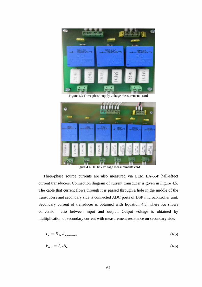
64
Figure 4.3 Three phase supply voltage measurements card
Figure 4.4 DC link voltage measurements card
Three-phase source currents are also measured via LEM LA-55P hall-effect
current transducers. Connection diagram of current transducer is given in Figure 4.5.
The cable that current flows through it is passed through a hole in the middle of the
transducers and secondary side is connected ADC ports of DSP microcontroller unit.
Secondary current of transducer is obtained with Equation 4.5, where KN shows
conversion ratio between input and output. Output voltage is obtained by
multiplication of secondary current with measurement resistance on secondary side.
measuredNs IKI . (4.5)
msout RIV . (4.6)
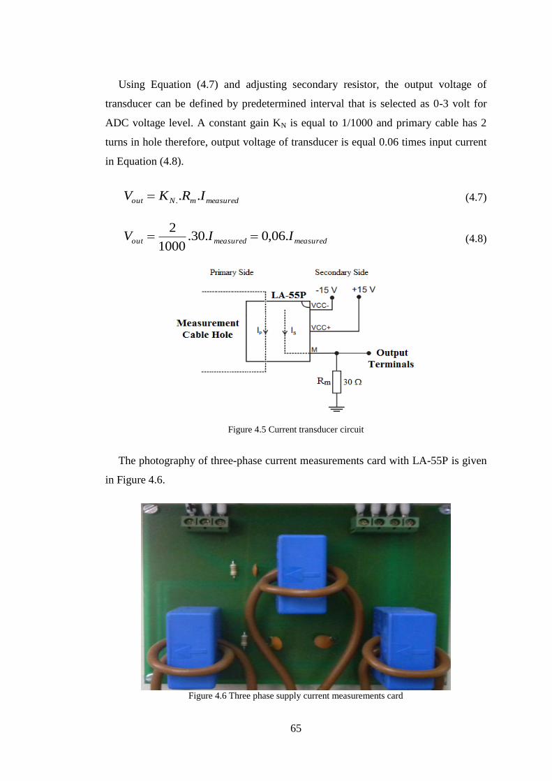
65
Using Equation (4.7) and adjusting secondary resistor, the output voltage of
transducer can be defined by predetermined interval that is selected as 0-3 volt for
ADC voltage level. A constant gain KN is equal to 1/1000 and primary cable has 2
turns in hole therefore, output voltage of transducer is equal 0.06 times input current
in Equation (4.8).
measuredmNout IRKV ... (4.7)
measuredmeasuredout IIV .06,0.30.1000
2 (4.8)
Figure 4.5 Current transducer circuit
The photography of three-phase current measurements card with LA-55P is given
in Figure 4.6.
Figure 4.6 Three phase supply current measurements card
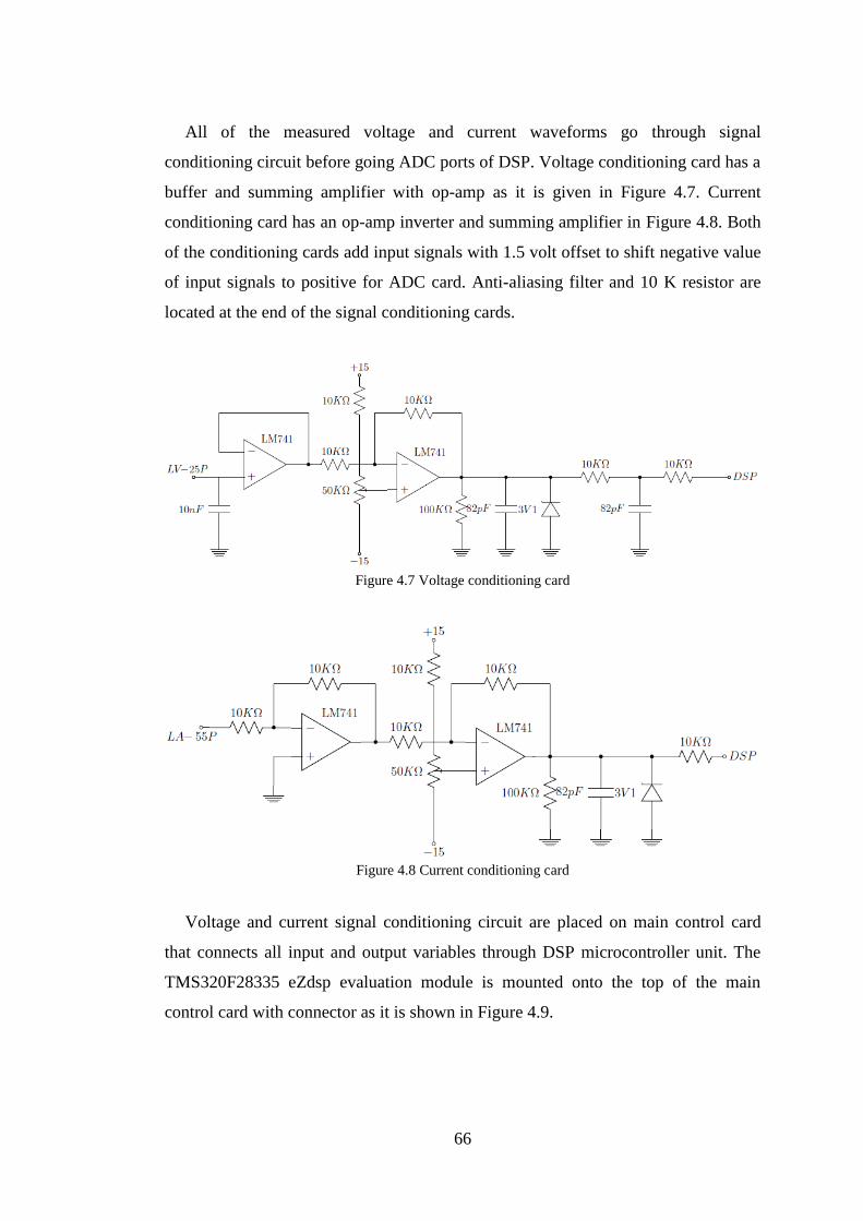
66
All of the measured voltage and current waveforms go through signal
conditioning circuit before going ADC ports of DSP. Voltage conditioning card has a
buffer and summing amplifier with op-amp as it is given in Figure 4.7. Current
conditioning card has an op-amp inverter and summing amplifier in Figure 4.8. Both
of the conditioning cards add input signals with 1.5 volt offset to shift negative value
of input signals to positive for ADC card. Anti-aliasing filter and 10 K resistor are
located at the end of the signal conditioning cards.
Figure 4.7 Voltage conditioning card
Figure 4.8 Current conditioning card
Voltage and current signal conditioning circuit are placed on main control card
that connects all input and output variables through DSP microcontroller unit. The
TMS320F28335 eZdsp evaluation module is mounted onto the top of the main
control card with connector as it is shown in Figure 4.9.
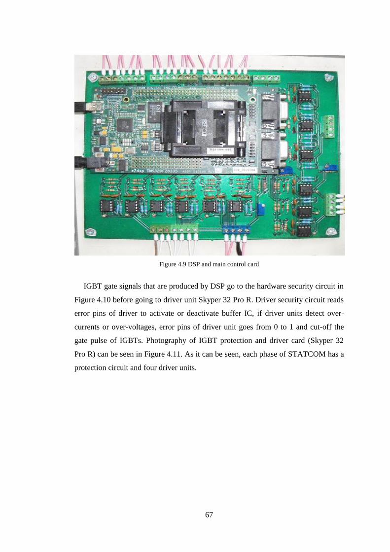
67
Figure 4.9 DSP and main control card
IGBT gate signals that are produced by DSP go to the hardware security circuit in
Figure 4.10 before going to driver unit Skyper 32 Pro R. Driver security circuit reads
error pins of driver to activate or deactivate buffer IC, if driver units detect over-
currents or over-voltages, error pins of driver unit goes from 0 to 1 and cut-off the
gate pulse of IGBTs. Photography of IGBT protection and driver card (Skyper 32
Pro R) can be seen in Figure 4.11. As it can be seen, each phase of STATCOM has a
protection circuit and four driver units.
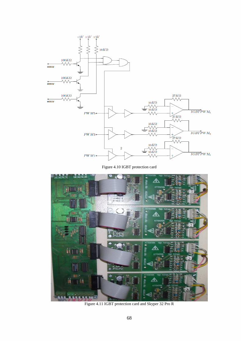
68
Figure 4.10 IGBT protection card
Figure 4.11 IGBT protection card and Skyper 32 Pro R
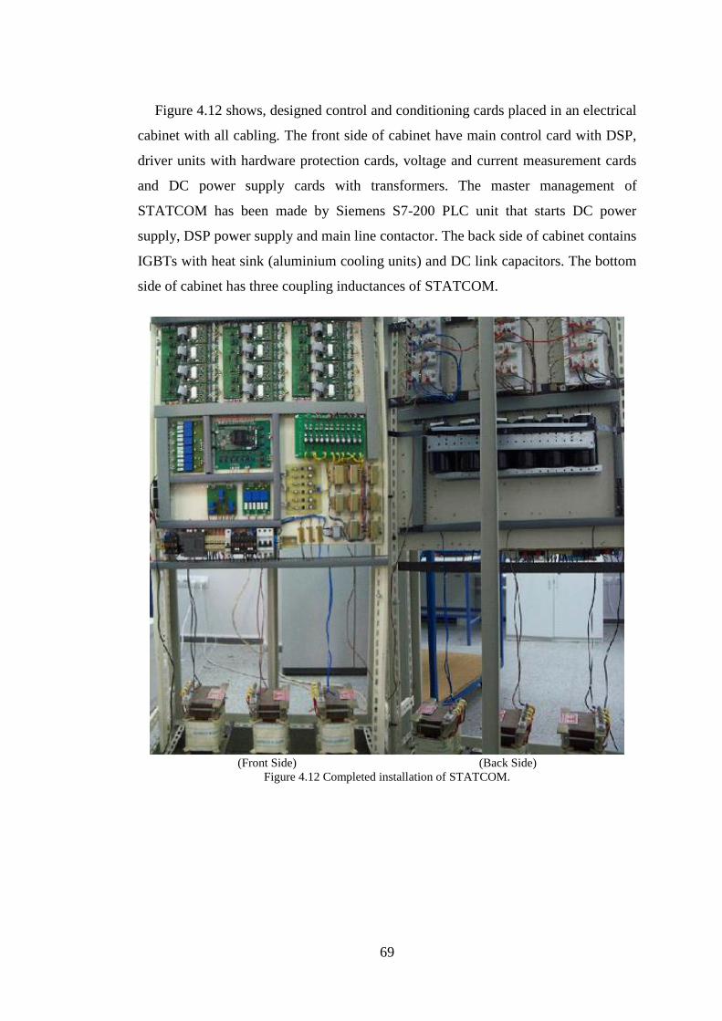
69
Figure 4.12 shows, designed control and conditioning cards placed in an electrical
cabinet with all cabling. The front side of cabinet have main control card with DSP,
driver units with hardware protection cards, voltage and current measurement cards
and DC power supply cards with transformers. The master management of
STATCOM has been made by Siemens S7-200 PLC unit that starts DC power
supply, DSP power supply and main line contactor. The back side of cabinet contains
IGBTs with heat sink (aluminium cooling units) and DC link capacitors. The bottom
side of cabinet has three coupling inductances of STATCOM.
(Front Side) (Back Side)
Figure 4.12 Completed installation of STATCOM.
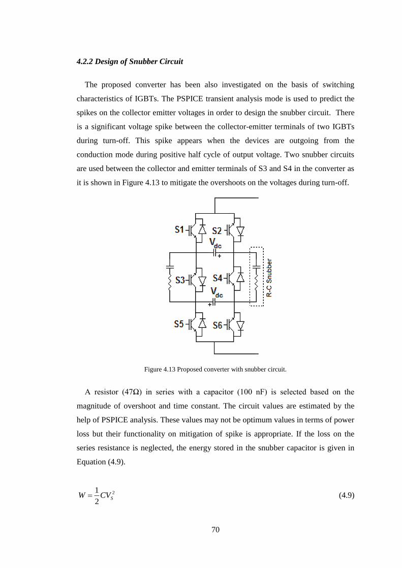
70
4.2.2 Design of Snubber Circuit
The proposed converter has been also investigated on the basis of switching
characteristics of IGBTs. The PSPICE transient analysis mode is used to predict the
spikes on the collector emitter voltages in order to design the snubber circuit. There
is a significant voltage spike between the collector-emitter terminals of two IGBTs
during turn-off. This spike appears when the devices are outgoing from the
conduction mode during positive half cycle of output voltage. Two snubber circuits
are used between the collector and emitter terminals of S3 and S4 in the converter as
it is shown in Figure 4.13 to mitigate the overshoots on the voltages during turn-off.
Figure 4.13 Proposed converter with snubber circuit.
A resistor (47Ω) in series with a capacitor (100 nF) is selected based on the
magnitude of overshoot and time constant. The circuit values are estimated by the
help of PSPICE analysis. These values may not be optimum values in terms of power
loss but their functionality on mitigation of spike is appropriate. If the loss on the
series resistance is neglected, the energy stored in the snubber capacitor is given in
Equation (4.9).
2
2
1SCVW (4.9)

71
This energy is transferred mostly to the resistor during conduction time of IGBT.
The transfer of energy is repeated twice in each period of converter output voltage.
Hence, the power absorbed by the resistor can be calculated from the Equation
(4.10).
fCVP S
2 (4.10)
Additional losses may occur due to the forward and reverse recovery process of
snubber diodes in converter, but this effect is not investigated in this work.
Simulation and experimental results after connecting the snubber circuits are given
in Figures 4.14 and Figure 4.15. The peak value of snubber current is limited by the
snubber resistance as it is seen in Figure 4.14. The time constant of snubber circuit
(4.7 s ) is small enough compared to the shortest conduction time of IGBT that is
62.5s, appearing from sampling frequency of DSP (16 kHz.). The shortest expected
on-time for the IGBT is around sampling period, if device changes status at two
consecutive sampling. The peak value of spike on collector emitter voltage is around
1.2 times of the DC link voltage (sum of two capacitor voltages) as it is observed in
Figure 4.15a. The maximum level of converter output voltage is equal to the sum of
two capacitor voltages as it is shown in Figure 4.15b.
Figure 4.14 a) Snubber current in simulation from PSPICE b) Snubber current in experiment
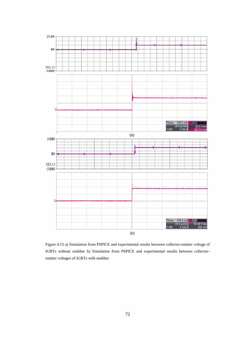
72
Figure 4.15 a) Simulation from PSPICE and experimental results between collector-emitter voltage of
IGBTs without snubber b) Simulation from PSPICE and experimental results between collector-
emitter voltages of IGBTs with snubber
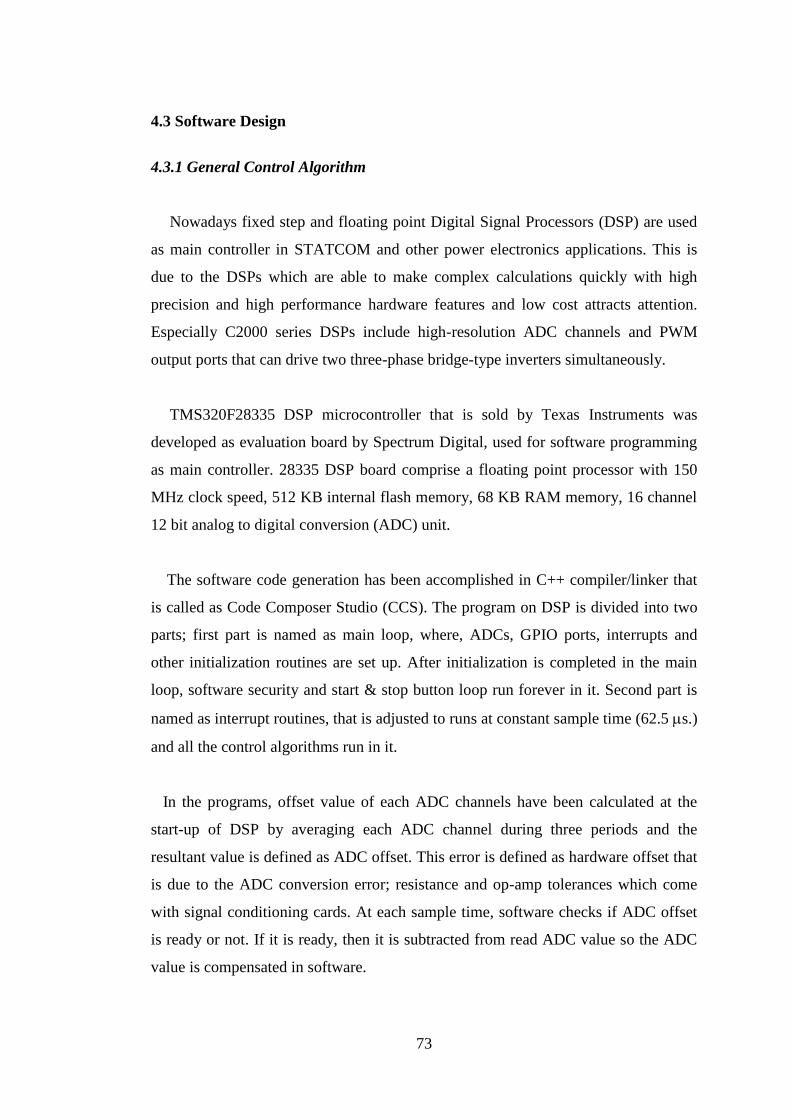
73
4.3 Software Design
4.3.1 General Control Algorithm
Nowadays fixed step and floating point Digital Signal Processors (DSP) are used
as main controller in STATCOM and other power electronics applications. This is
due to the DSPs which are able to make complex calculations quickly with high
precision and high performance hardware features and low cost attracts attention.
Especially C2000 series DSPs include high-resolution ADC channels and PWM
output ports that can drive two three-phase bridge-type inverters simultaneously.
TMS320F28335 DSP microcontroller that is sold by Texas Instruments was
developed as evaluation board by Spectrum Digital, used for software programming
as main controller. 28335 DSP board comprise a floating point processor with 150
MHz clock speed, 512 KB internal flash memory, 68 KB RAM memory, 16 channel
12 bit analog to digital conversion (ADC) unit.
The software code generation has been accomplished in C++ compiler/linker that
is called as Code Composer Studio (CCS). The program on DSP is divided into two
parts; first part is named as main loop, where, ADCs, GPIO ports, interrupts and
other initialization routines are set up. After initialization is completed in the main
loop, software security and start & stop button loop run forever in it. Second part is
named as interrupt routines, that is adjusted to runs at constant sample time (62.5 s.)
and all the control algorithms run in it.
In the programs, offset value of each ADC channels have been calculated at the
start-up of DSP by averaging each ADC channel during three periods and the
resultant value is defined as ADC offset. This error is defined as hardware offset that
is due to the ADC conversion error; resistance and op-amp tolerances which come
with signal conditioning cards. At each sample time, software checks if ADC offset
is ready or not. If it is ready, then it is subtracted from read ADC value so the ADC
value is compensated in software.
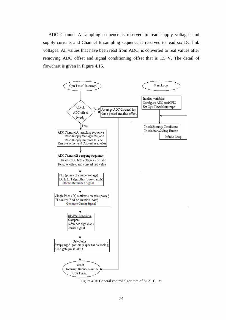
74
ADC Channel A sampling sequence is reserved to read supply voltages and
supply currents and Channel B sampling sequence is reserved to read six DC link
voltages. All values that have been read from ADC, is converted to real values after
removing ADC offset and signal conditioning offset that is 1.5 V. The detail of
flowchart is given in Figure 4.16.
Figure 4.16 General control algorithm of STATCOM
75
4.3.2 Design of PLL
Phase information of supply voltage is needed for balancing DC capacitor
voltages. Three-phase PLL algorithm given in Figure 4.17 is used to obtain phase
information. A commonly used three phase PLL method is based on Clarke-Park
transformation, where supply voltages are transformed to stationary reference frames
by Clarke transform (CT) given in (4.11) then the park transform (PT) given in (4.12)
is applied to synchronize it to the supply frequency (Chattopadhyay, 2011). Phase
information is obtained by passing direct axis component of supply voltages (Vd) on
PI controller and adding output of PI to the reference frequency (wref), if the result
(w*) is integrated then phase information is obtained (Phipps, 2006), (Chung, 2000).
2
1
2
1
2
12
3
2
30
2
1
2
11
3
2TC (4.11)
cossin
sincosTP (4.12)
The PLL application provides θ and the supply voltages as follows;
SinVa (4.13)
)3
2(
SinVb (4.14)
)3
2(
SinVc (4.15)
Therefore, the phase difference () between supply and STATCOM voltage can
be added to θ in order to control real power flow.
76
Figure 4.17 Block diagram of traditional PLL
4.3.3 Application of Digital PI Controller
In the closed loop control of reactive power and DC link voltage, the error
between the reference and actual values are passed through a proportional-integral
(PI) controllers. Analog PI controller is expressed in Equation (4.16). The output of
analog PI controller is evaluated expressed by error signal ((t)), proportional (Kp)
and integral (Ki) error gains terms.
dttKtKtu iP )()()( (4.16)
In DSP microcontroller, discrete (digital) form of the analog PI controller is used.
The output of digital PI controller is evaluated in terms of error, change of error and
sampling time (Ts) as follows:
)()()( SESCES TnKTnKTnu (4.17)
Integral time constant KE is a function of sampling period. It is obtained by
multiplying of integral gain (Ki) with sampling period (Ts) (KE=Ki.Ts). The change of
error constant (KCE) is equal to proportional gain (Kp) (KCE= Kp). It is defined in DSP

77
code as constant at the initialization. The block diagram of the digital PI controller is
given in Figure 4.18.
Figure 4.18 Block diagram of PI controller.
4.3.4 Design of DC Link Voltage Controller
The DC link capacitors are charged at the beginning by the three-phase
uncontrolled rectifier built with the anti-parallel diodes of IGBTs in voltage source
converter. There are three resistors (in parallel with electro-mechanical relays)
connected between source voltages and converter. At the starting the relays are kept
open and inrush current through the capacitors and diodes is reduced. After charging
up the capacitors the switches are closed and the resistors are bypassed.
Figure 4.19 charging resistor connection in star connected STATCOM
The converter draws the active power demanded by the internal resistances of DC
link capacitors, switching inductors and switching loss of IGBTs in voltage source
converter.

78
DC link voltage error signal is calculated by subtracting DC link voltage from
reference value. Digital PI controller unit takes error signal and the result presents
the power angle (). Adding this angle to the output of PLL, reference sinusoidal
signal is generated.
4.3.5 Programming of Single Phase P-Q
The reactive power demanded by the load is estimated by using single phase P-Q
method. According to this algorithm instantaneous active and reactive power can be
calculated using components of real and imaginary parts of voltage and current under
balanced sinusoidal AC voltage source. In program code the imaginary part of the
current is obtained by using buffer. The size of the buffer (80 samples) is determined
by the sampling time so as to delay the voltage and current by 90 degrees. Cross-
multiplication of real and imaginary components of voltage and current are given in
(4.18) yields instantaneous reactive power (Qact).
ivivQact .. (4.18)
In software, first order digital low pass filter is added to eliminate the harmonic
components on estimated reactive power. Filter with a cut-off frequency of 80 Hz is
programmed in the DSP microcontroller. Transfer function of the digital filter is
given in Equation (4.20).
]1[)1(][][ kQKkQKkQ filteredactfiltered (4.19)
1).1(1)(
zK
KzH (4.20)
Figure 4.20 First order low pass digital filter
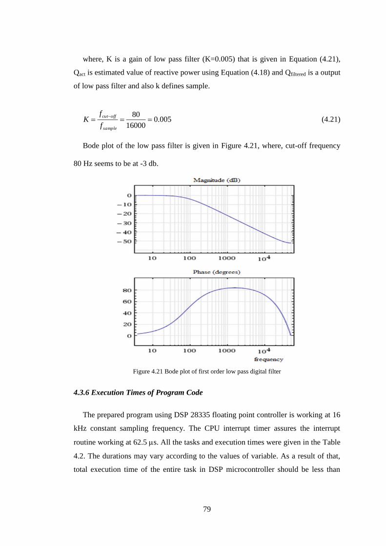
79
where, K is a gain of low pass filter (K=0.005) that is given in Equation (4.21),
Qact is estimated value of reactive power using Equation (4.18) and Qfiltered is a output
of low pass filter and also k defines sample.
005.016000
80
sample
offcut
f
fK (4.21)
Bode plot of the low pass filter is given in Figure 4.21, where, cut-off frequency
80 Hz seems to be at -3 db.
Figure 4.21 Bode plot of first order low pass digital filter
4.3.6 Execution Times of Program Code
The prepared program using DSP 28335 floating point controller is working at 16
kHz constant sampling frequency. The CPU interrupt timer assures the interrupt
routine working at 62.5 s. All the tasks and execution times were given in the Table
4.2. The durations may vary according to the values of variable. As a result of that,
total execution time of the entire task in DSP microcontroller should be less than
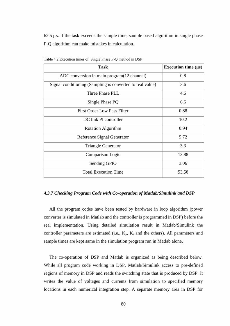
80
62.5 s. If the task exceeds the sample time, sample based algorithm in single phase
P-Q algorithm can make mistakes in calculation.
Table 4.2 Execution times of Single Phase P-Q method in DSP
Task Execution time (μs)
ADC conversion in main program(12 channel) 0.8
Signal conditioning (Sampling is converted to real value) 3.6
Three Phase PLL 4.6
Single Phase PQ 6.6
First Order Low Pass Filter 0.88
DC link PI controller 10.2
Rotation Algorithm 0.94
Reference Signal Generator 5.72
Triangle Generator 3.3
Comparison Logic 13.88
Sending GPIO 3.06
Total Execution Time 53.58
4.3.7 Checking Program Code with Co-operation of Matlab/Simulink and DSP
All the program codes have been tested by hardware in loop algorithm (power
converter is simulated in Matlab and the controller is programmed in DSP) before the
real implementation. Using detailed simulation result in Matlab/Simulink the
controller parameters are estimated (i.e., Kp, Ki and the others). All parameters and
sample times are kept same in the simulation program run in Matlab alone.
The co-operation of DSP and Matlab is organized as being described below.
While all program code working in DSP, Matlab/Simulink access to pre-defined
regions of memory in DSP and reads the switching state that is produced by DSP. It
writes the value of voltages and currents from simulation to specified memory
locations in each numerical integration step. A separate memory area in DSP for
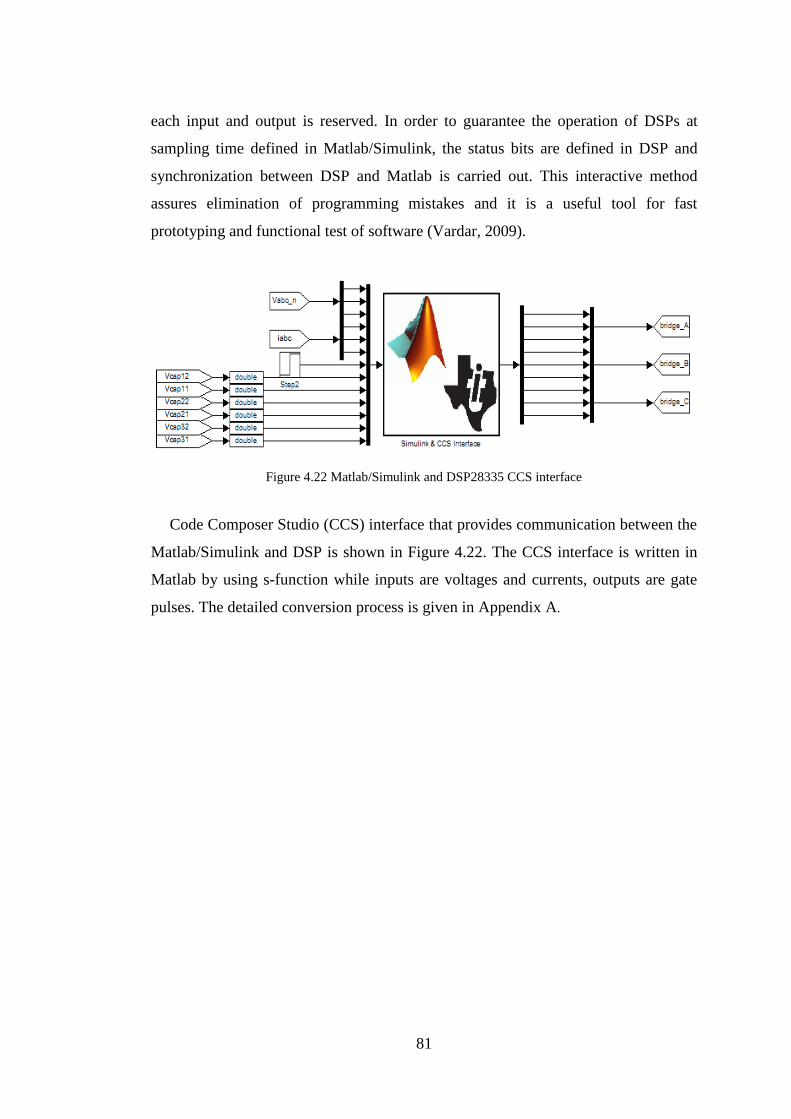
81
each input and output is reserved. In order to guarantee the operation of DSPs at
sampling time defined in Matlab/Simulink, the status bits are defined in DSP and
synchronization between DSP and Matlab is carried out. This interactive method
assures elimination of programming mistakes and it is a useful tool for fast
prototyping and functional test of software (Vardar, 2009).
Figure 4.22 Matlab/Simulink and DSP28335 CCS interface
Code Composer Studio (CCS) interface that provides communication between the
Matlab/Simulink and DSP is shown in Figure 4.22. The CCS interface is written in
Matlab by using s-function while inputs are voltages and currents, outputs are gate
pulses. The detailed conversion process is given in Appendix A.
82
CHAPTER FIVE
MODELLING OF STATCOM
5.1 Introductory Remarks
In literature, analytical model of cascaded multilevel converter can be obtained
using three-phase d-q reference frame theory and examined by using linearization
equations (Kumar, 2009). The source voltages are balanced and have sinusoidal
waveform. Furthermore, all switches and capacitors are assumed to be lossless and
harmonics of converter voltage are neglected. A simplified model is based on AC
small signal model that was derived from average value model of STATCOM.
Accuracy of model was verified by comparing dynamic responses with computer
simulation program. A feedback control unit is designed to balance DC link voltages
in the model (Sirisukprasert, 2003). Three-phase model of STATCOM is
transformed to synchronously rotating reference frame and nonlinearity of state
equations on control angle are linearized in the d-q frame. The stability of
STATCOM is examined independently from control strategy (Rao, 2000).
Single phase converters can also be examined in d-q reference frame. Model of
single phase inverter was obtained in two phase rotating reference frame (Zhang,
2002). By using two phase transformation matrix, single phase H-bridge converter is
transformed into the d-q reference frame. After transformation, open loop and closed
loop model are studied for inverter mode (Roshan, 2007).
In this chapter, a detailed model of single phase AC to DC converter has been
investigated at the synchronously rotating reference frame which is useful to generate
average value model of switching functions and the complete block diagram of the
system with adequate transfer functions.
Proposed multilevel converter structure has two separated DC sources and
produces five different output voltage levels: +2Vdc, +Vdc, 0, -Vdc, -2Vdc by
combination of six semiconductors, namely S1, S2, S3, S4, S5 and S6. Using
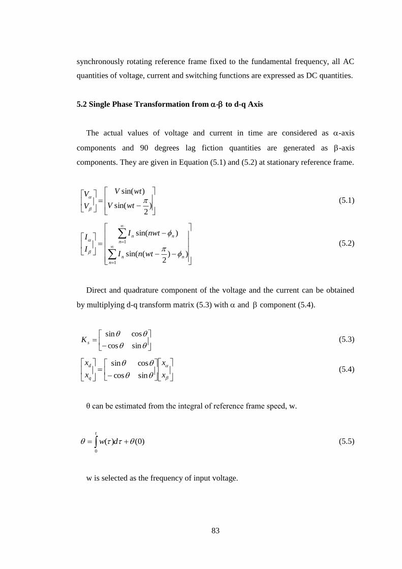
83
synchronously rotating reference frame fixed to the fundamental frequency, all AC
quantities of voltage, current and switching functions are expressed as DC quantities.
5.2 Single Phase Transformation from - to d-q Axis
The actual values of voltage and current in time are considered as -axis
components and 90 degrees lag fiction quantities are generated as -axis
components. They are given in Equation (5.1) and (5.2) at stationary reference frame.
)2
sin(
)sin(
wtV
wtV
V
V (5.1)
1
1
))2
(sin(
)sin(
n
nn
n
nn
wtnI
nwtI
I
I
(5.2)
Direct and quadrature component of the voltage and the current can be obtained
by multiplying d-q transform matrix (5.3) with and component (5.4).
sincos
cossinsK (5.3)
x
x
x
x
q
d
sincos
cossin (5.4)
θ can be estimated from the integral of reference frame speed, w.
)0()(0
dw
t
(5.5)
w is selected as the frequency of input voltage.
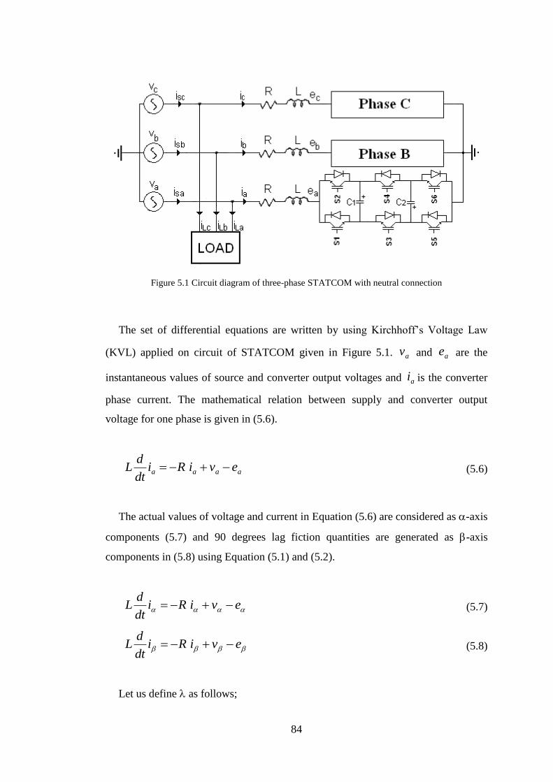
84
Figure 5.1 Circuit diagram of three-phase STATCOM with neutral connection
The set of differential equations are written by using Kirchhoff’s Voltage Law
(KVL) applied on circuit of STATCOM given in Figure 5.1. av and ae are the
instantaneous values of source and converter output voltages and ai is the converter
phase current. The mathematical relation between supply and converter output
voltage for one phase is given in (5.6).
aaaa eviRidt
dL (5.6)
The actual values of voltage and current in Equation (5.6) are considered as -axis
components (5.7) and 90 degrees lag fiction quantities are generated as -axis
components in (5.8) using Equation (5.1) and (5.2).
eviRidt
dL (5.7)
eviRidt
dL (5.8)
Let us define as follows;

85
iL. (5.9)
Differential equation in stationary reference frame can be rewritten as (5.10).
eviRp . (5.10)
where p is the derivative term (dt
dp ). R is the resistance of coupling
inductance. Hence,
R
RR
0
0 (5.11)
Using Transformation matrix Ks all variable are transformed into synchronous
rotating reference frame. dqSK 1 , dqRR , dqS iKi 1 , dqS vKv 1 and
dqS eKe 1 are substituted into (5.10) and Equation (5.12) is obtained.
dqSdqSdqSdqS eKvKiRKKp 1111 ).( (5.12)
If both sides are multiplied by transformation matrix Ks:
dqSSdqSSdqSSdqSS eKKvKKiKRKKpK 1111 ).( (5.13)
Equation (5.14) is obtained by taking derivative term at left side of Equation
(5.13), where derivative of inverse transformation matrix ].[ 1
SKp is given in (5.15)
and multiplication result with transformation matrix ][ 1
SS KpK is given in (5.16).
dqdqdqSdqSdqSSqdSS eiKRKpKKKpK 111 )(])[( (5.14)
cossin
sincos].[ 1
SKp (5.15)
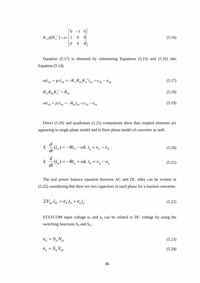
86
000
001
010
][ 1 SS KpK (5.16)
Equation (5.17) is obtained by substituting Equations (5.15) and (5.16) into
Equation (5.14).
dqdqdqSdqSdqqd eiKRKp 1. (5.17)
dqSdqS RKRK 1 (5.18)
dqdqdqdqdqqd eiRp . (5.19)
Direct (5.20) and quadrature (5.21) components show that coupled elements are
appearing in single phase model and in three phase model of converter as well.
ddqdd eviLRiidt
dL )( (5.20)
qqdqq eviLRiidt
dL )( (5.21)
The real power balance equation between AC and DC sides can be written in
(5.22) considering that there are two capacitors in each phase for a lossless converter.
qqdddcdc ieieiV ....2 (5.22)
STATCOM input voltage ed and eq can be related to DC voltage by using the
switching functions Sd and Sq.
dcdd VSe . (5.23)
dcqq VSe . (5.24)
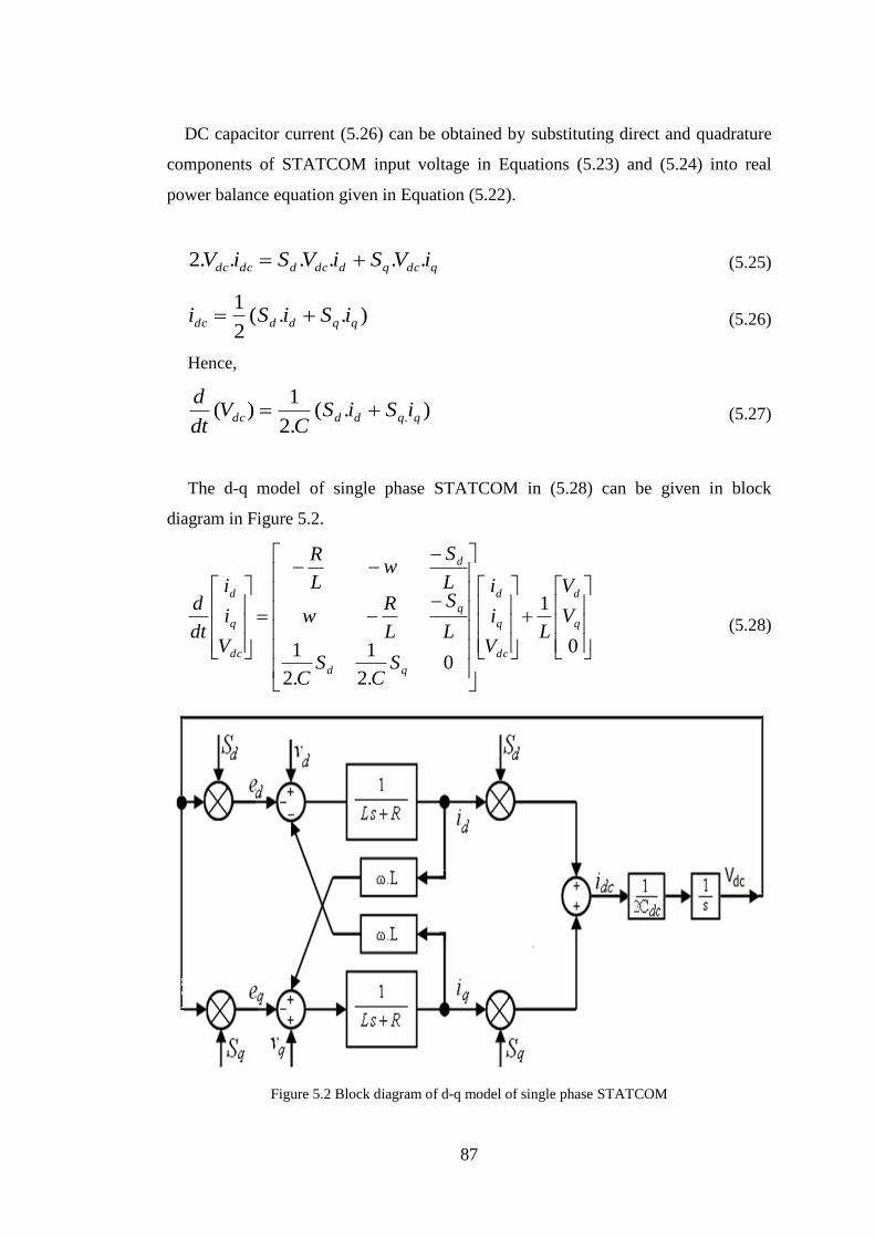
87
DC capacitor current (5.26) can be obtained by substituting direct and quadrature
components of STATCOM input voltage in Equations (5.23) and (5.24) into real
power balance equation given in Equation (5.22).
qdcqddcddcdc iVSiVSiV ......2 (5.25)
)..(2
1qqdddc iSiSi (5.26)
Hence,
).(.2
1)( . qqdddc iSiS
CV
dt
d (5.27)
The d-q model of single phase STATCOM in (5.28) can be given in block
diagram in Figure 5.2.
0
1
0.2
1
.2
1
q
d
dc
q
d
qd
q
d
dc
q
d
V
V
LV
i
i
SC
SC
L
S
L
Rw
L
Sw
L
R
V
i
i
dt
d (5.28)
Figure 5.2 Block diagram of d-q model of single phase STATCOM
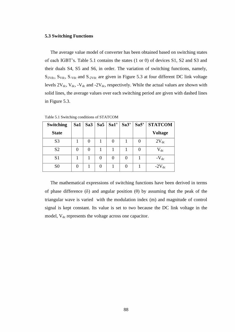
88
5.3 Switching Functions
The average value model of converter has been obtained based on switching states
of each IGBT’s. Table 5.1 contains the states (1 or 0) of devices S1, S2 and S3 and
their duals S4, S5 and S6, in order. The variation of switching functions, namely,
S2Vdc, SVdc, S-Vdc and S-2Vdc are given in Figure 5.3 at four different DC link voltage
levels 2Vdc, Vdc, -Vdc and -2Vdc, respectively. While the actual values are shown with
solid lines, the average values over each switching period are given with dashed lines
in Figure 5.3.
Table 5.1 Switching conditions of STATCOM
Switching
State
Sa1 Sa3 Sa5 Sa1’ Sa3’ Sa5’ STATCOM
Voltage
S3 1 0 1 0 1 0 2Vdc
S2 0 0 1 1 1 0 Vdc
S1 1 1 0 0 0 1 -Vdc
S0 0 1 0 1 0 1 -2Vdc
The mathematical expressions of switching functions have been derived in terms
of phase difference () and angular position (θ) by assuming that the peak of the
triangular wave is varied with the modulation index (m) and magnitude of control
signal is kept constant. Its value is set to two because the DC link voltage in the
model, Vdc represents the voltage across one capacitor.

89
Figure 5.3 Switching function a) 2Vdc b) Vdc c) -Vdc d) -2Vdc
When STATCOM input voltage is reached to 2Vdc level indicated in Figure 5.3a,
average value of switching function is modelled by using equation in (5.29). Here m
is modulation index, is load angle and is angular position signals.
otherwise
mmwt
mS Vdc
,0
)2
(sin)2
(sin,1)sin(2 11
2
(5.29)
When STATCOM input voltage is reached to Vdc level, seen in Figure 5.3b, the
average value of switching function which is modelled in Equation (5.30). Here the
value of switching function is determined by angular position signals.
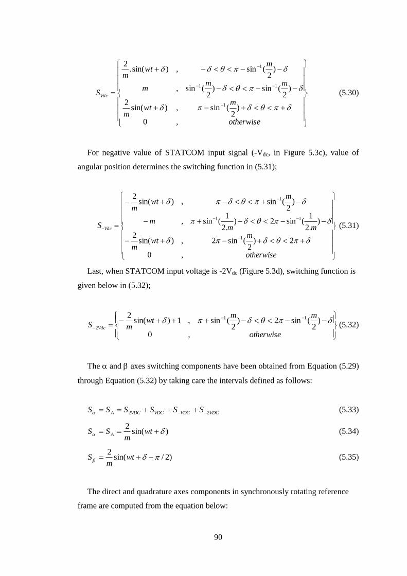
90
otherwise
mwt
m
mmm
mwt
m
SVdc
,0
)2
(sin,)sin(2
)2
(sin)2
(sin,
)2
(sin,)sin(.2
1
11
1
(5.30)
For negative value of STATCOM input signal (-Vdc, in Figure 5.3c), value of
angular position determines the switching function in (5.31);
otherwise
mwt
m
mmm
mwt
m
S Vdc
,0
2)2
(sin2,)sin(2
).2
1(sin2)
.2
1(sin,
)2
(sin,)sin(2
1
11
1
(5.31)
Last, when STATCOM input voltage is -2Vdc (Figure 5.3d), switching function is
given below in (5.32);
otherwise
mmwt
mS Vdc
,0
)2
(sin2)2
(sin,1)sin(2 11
2
(5.32)
The and axes switching components have been obtained from Equation (5.29)
through Equation (5.32) by taking care the intervals defined as follows:
VDCVDCVDCVDCA SSSSSS 22 (5.33)
)sin(2
wtm
SS A (5.34)
)2/sin(2
wtm
S (5.35)
The direct and quadrature axes components in synchronously rotating reference
frame are computed from the equation below:
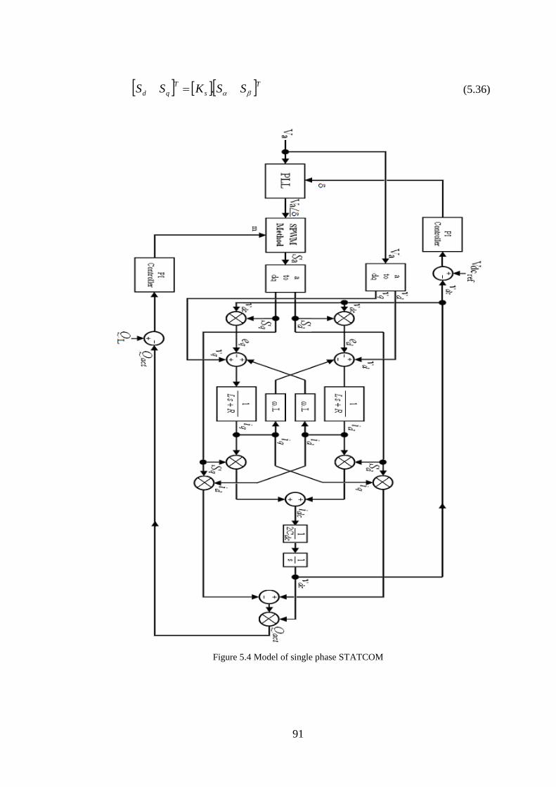
91
Ts
T
qd SSKSS . (5.36)
Figure 5.4 Model of single phase STATCOM
92
A pure sinusoidal function obtained in Equations (5.34) and (5.35) shows that the
proposed converter can be controlled by the SPWM modulation technique by using
the variables of modulation index and power angle. The analysis of STATCOM has
been carried out by using the complete model given in Figure 5.4.
In Figure 5.4, angular position (θ) is obtained by using PLL. STATCOM phase
information (Va) is obtained by adding angular position of source voltage to DC
link PI controller output (). SPWM controller uses phase information and
modulation index that is obtained from the output of reactive power PI controller.
Output of SPWM controller is switching function of phase A which is transformed to
d-q reference frame by multiplying Ks transform.
5.4 Comparing Results of Model with Matlab Simulation
Results obtained from the analysis of model are compared with ones from the
detailed simulation prepared in Matlab/Simulink. Figure 5.5 shows that the average
value model gives almost the same values with the results of Matlab simulation,
when the amplitude and rise time are compared during transient applications. It
should be noted that the simulation results at the same operating condition have been
compared to experimental ones as well.
When the simulation time is equal to 2 seconds, 350 VAR inductive load is
connected to system and STATCOM generates 350 VAR reactive powers for
compensation. After the system reaches the steady state level, 350 VAR capacitive
load is added to system at time of 4 seconds, hence STATCOM draws 350 VAR
reactive powers from system to bring the source power factor to unity.
When the results of Matlab/Simulink and single phase d-q model are compared
with each other, all response time and amplitude variable are compatible.
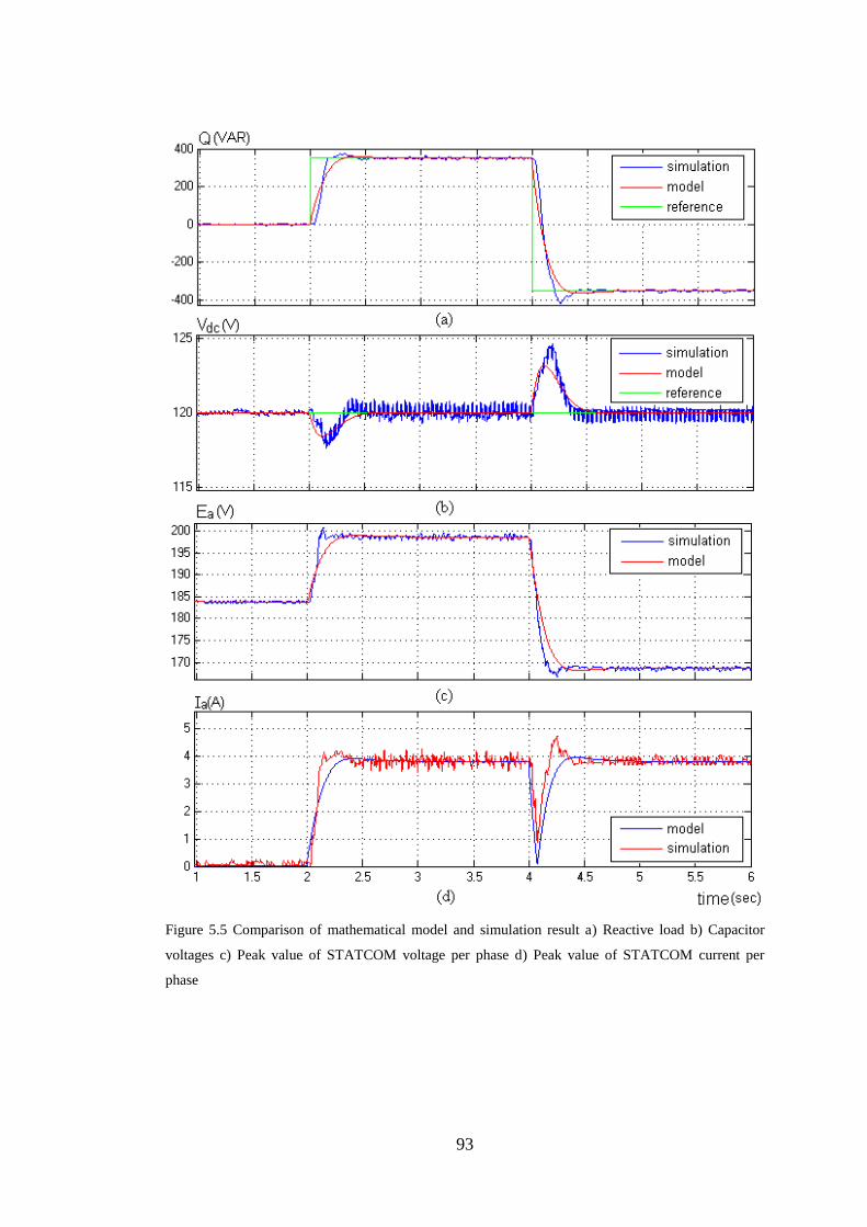
93
Figure 5.5 Comparison of mathematical model and simulation result a) Reactive load b) Capacitor
voltages c) Peak value of STATCOM voltage per phase d) Peak value of STATCOM current per
phase
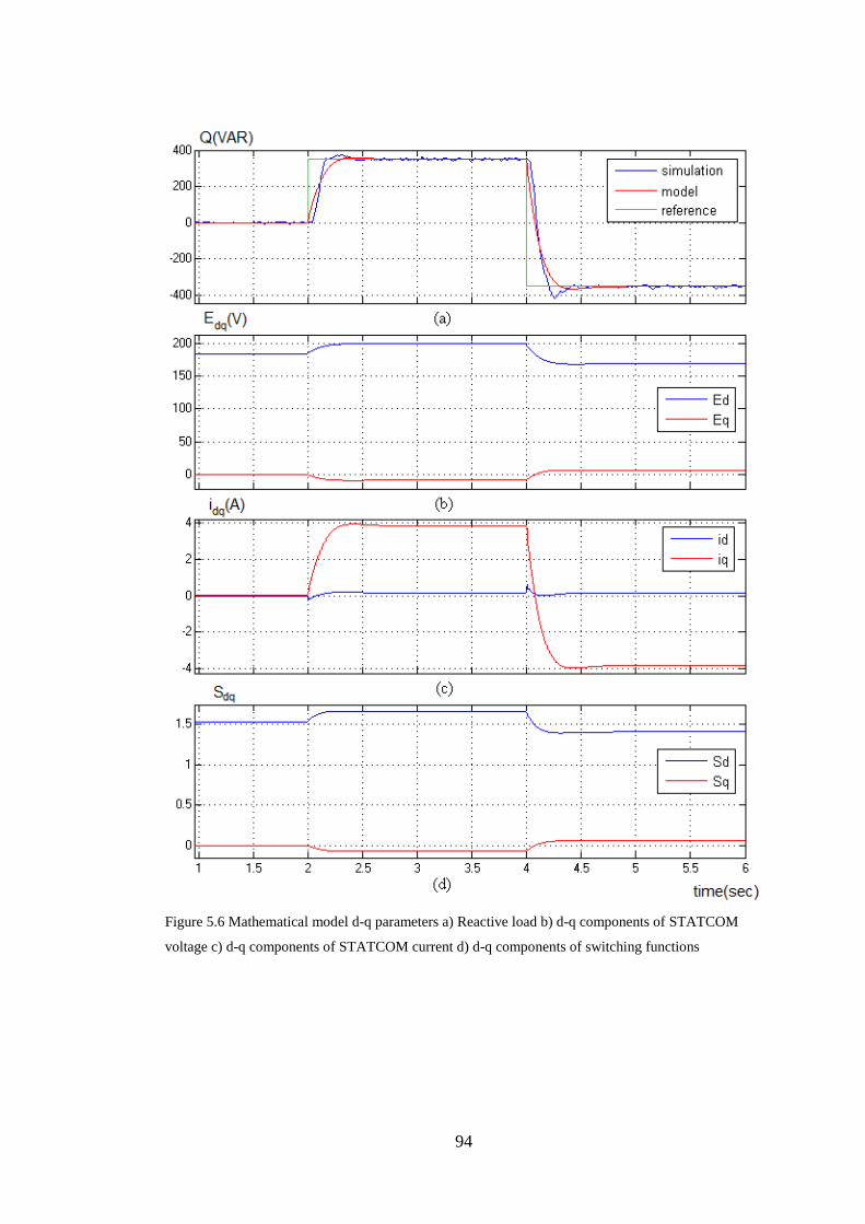
94
Figure 5.6 Mathematical model d-q parameters a) Reactive load b) d-q components of STATCOM
voltage c) d-q components of STATCOM current d) d-q components of switching functions
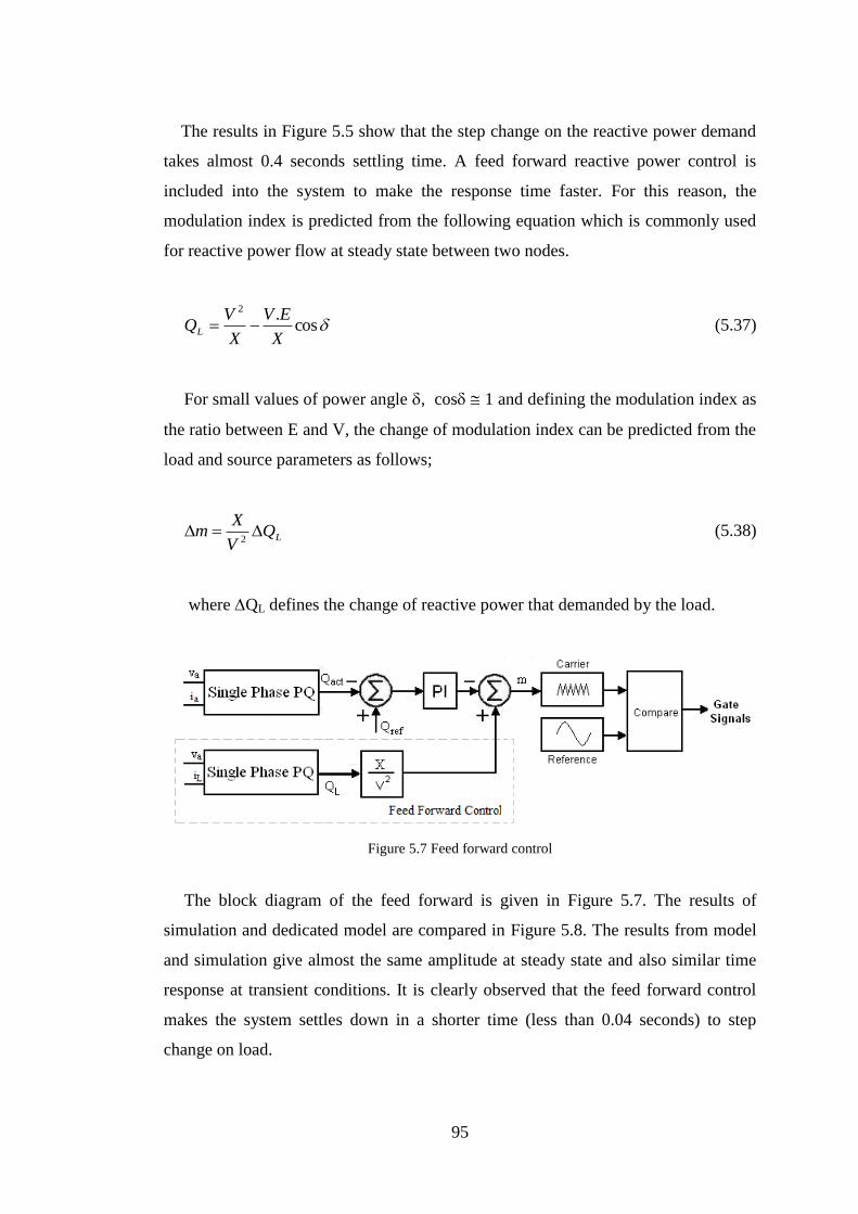
95
The results in Figure 5.5 show that the step change on the reactive power demand
takes almost 0.4 seconds settling time. A feed forward reactive power control is
included into the system to make the response time faster. For this reason, the
modulation index is predicted from the following equation which is commonly used
for reactive power flow at steady state between two nodes.
cos.2
X
EV
X
VQL (5.37)
For small values of power angle , cos 1 and defining the modulation index as
the ratio between E and V, the change of modulation index can be predicted from the
load and source parameters as follows;
LQV
Xm
2 (5.38)
where QL defines the change of reactive power that demanded by the load.
Figure 5.7 Feed forward control
The block diagram of the feed forward is given in Figure 5.7. The results of
simulation and dedicated model are compared in Figure 5.8. The results from model
and simulation give almost the same amplitude at steady state and also similar time
response at transient conditions. It is clearly observed that the feed forward control
makes the system settles down in a shorter time (less than 0.04 seconds) to step
change on load.
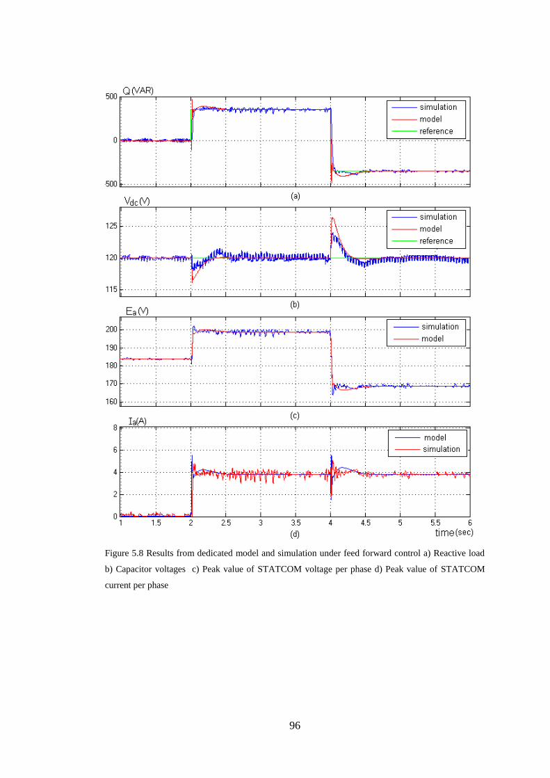
96
Figure 5.8 Results from dedicated model and simulation under feed forward control a) Reactive load
b) Capacitor voltages c) Peak value of STATCOM voltage per phase d) Peak value of STATCOM
current per phase
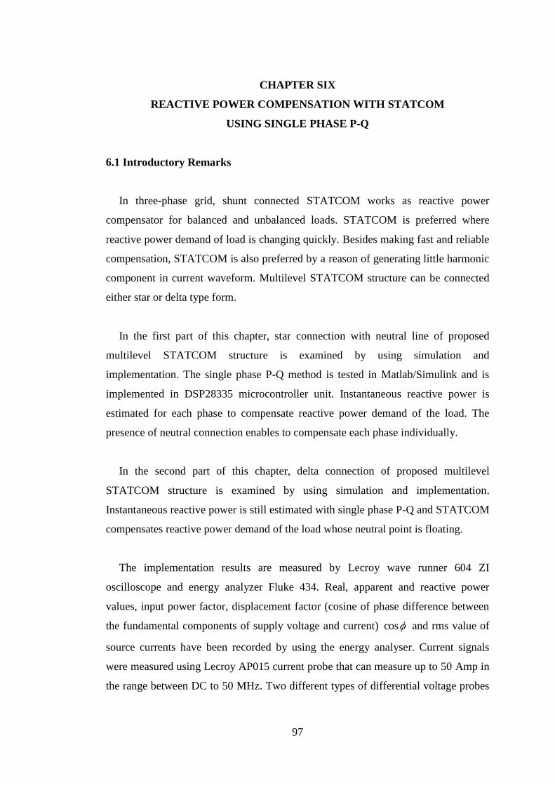
97
CHAPTER SIX
REACTIVE POWER COMPENSATION WITH STATCOM
USING SINGLE PHASE P-Q
6.1 Introductory Remarks
In three-phase grid, shunt connected STATCOM works as reactive power
compensator for balanced and unbalanced loads. STATCOM is preferred where
reactive power demand of load is changing quickly. Besides making fast and reliable
compensation, STATCOM is also preferred by a reason of generating little harmonic
component in current waveform. Multilevel STATCOM structure can be connected
either star or delta type form.
In the first part of this chapter, star connection with neutral line of proposed
multilevel STATCOM structure is examined by using simulation and
implementation. The single phase P-Q method is tested in Matlab/Simulink and is
implemented in DSP28335 microcontroller unit. Instantaneous reactive power is
estimated for each phase to compensate reactive power demand of the load. The
presence of neutral connection enables to compensate each phase individually.
In the second part of this chapter, delta connection of proposed multilevel
STATCOM structure is examined by using simulation and implementation.
Instantaneous reactive power is still estimated with single phase P-Q and STATCOM
compensates reactive power demand of the load whose neutral point is floating.
The implementation results are measured by Lecroy wave runner 604 ZI
oscilloscope and energy analyzer Fluke 434. Real, apparent and reactive power
values, input power factor, displacement factor (cosine of phase difference between
the fundamental components of supply voltage and current) cos and rms value of
source currents have been recorded by using the energy analyser. Current signals
were measured using Lecroy AP015 current probe that can measure up to 50 Amp in
the range between DC to 50 MHz. Two different types of differential voltage probes
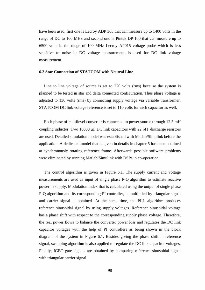
98
have been used, first one is Lecroy ADP 305 that can measure up to 1400 volts in the
range of DC to 100 MHz and second one is Pintek DP-100 that can measure up to
6500 volts in the range of 100 MHz Lecroy AP015 voltage probe which is less
sensitive to noise in DC voltage measurement, is used for DC link voltage
measurement.
6.2 Star Connection of STATCOM with Neutral Line
Line to line voltage of source is set to 220 volts (rms) because the system is
planned to be tested in star and delta connected configuration. Thus phase voltage is
adjusted to 130 volts (rms) by connecting supply voltage via variable transformer.
STATCOM DC link voltage reference is set to 110 volts for each capacitor as well.
Each phase of multilevel converter is connected to power source through 12.5 mH
coupling inductor. Two 10000 F DC link capacitors with 22 k discharge resistors
are used. Detailed simulation model was established with Matlab/Simulink before the
application. A dedicated model that is given in details in chapter 5 has been obtained
at synchronously rotating reference frame. Afterwards possible software problems
were eliminated by running Matlab/Simulink with DSPs in co-operation.
The control algorithm is given in Figure 6.1. The supply current and voltage
measurements are used as input of single phase P-Q algorithm to estimate reactive
power in supply. Modulation index that is calculated using the output of single phase
P-Q algorithm and its corresponding PI controller, is multiplied by triangular signal
and carrier signal is obtained. At the same time, the PLL algorithm produces
reference sinusoidal signal by using supply voltages. Reference sinusoidal voltage
has a phase shift with respect to the corresponding supply phase voltage. Therefore,
the real power flows to balance the converter power loss and regulates the DC link
capacitor voltages with the help of PI controllers as being shown in the block
diagram of the system in Figure 6.1. Besides giving the phase shift in reference
signal, swapping algorithm is also applied to regulate the DC link capacitor voltages.
Finally, IGBT gate signals are obtained by comparing reference sinusoidal signal
with triangular carrier signal.

99
Figure 6.1 Control schematic of star with neutral connected STATCOM
6.2.1 Balance Load in Parallel to Star-Connected STATCOM
In the first case, results of the balanced loading conditions for star connected
STATCOM have been obtained from simulation and implementation.
Five different balanced loading conditions have been used during the tests and
have been given in terms of real (P) and reactive (Q) powers in Table 6.1. Load 1
shows balanced resistive and inductive (R-L) load, load 2 shows balanced resistive
and capacitive (R-C) load, load 3 shows balanced resistive (R) load, load 4 shows
balanced inductive (L) load and load 5 shows balanced capacitive (C) load.

100
Table 6.1 Balanced loading conditions for star-connected STATCOM
Phase A Phase B Phase C
P
(W)
Q
(VAR)
P
(W)
Q
(VAR)
P
(W)
Q
(VAR)
Load 1 (Balanced R-L) 700 350 700 350 700 350
Load 2 (Balanced R-C) 700 -350 700 -350 700 -350
Load 3 (Balanced R) 700 0 700 0 700 0
Load 4 (Balanced L) 0 350 0 350 0 350
Load 5 (Balanced C) 0 -350 0 -350 0 -350
6.2.1.1 Balance R-L Load in Parallel to Star-Connected STATCOM
Figures 6.2 shows the simulation and implementation results of balanced R-L load
that compensated by STATCOM. The rms magnitude of STATCOM output voltage
is greater than supply voltage and STATCOM current leads voltage by 90 degrees. It
generates the reactive power and compensates the demand of inductive load. Figure
6.3 has the recorded values of powers, power factor, voltages and currents by using
the energy analyzer. The load power factor is 0.92 and real power demand is around
0.73 kW and reactive power demand is around 0.31 kVAR as it is given in Figure
6.3a. After activating the STATCOM, cosϕ becomes unity and reactive power
supplied from the source is going to zero as it is shown in Figure 6.2b. Some current
harmonics are observed on source current due to the switching ripple of STATCOM
as it is clearly realized from Figure 6.2c.
Start-up characteristics of STATCOM under R-L loading conditions can be seen
in Figure 6.4, where transient response of DC link voltage and current are in the safe
operating range. Proportional and Integral controller (PI) shows successful operation
under load.

101
Figure 6.2 Simulation and implementation result from balanced R-L load a) STATCOM voltage (V)
b) Source voltage (V) c) Source current (A) d) STATCOM current (A)
Figure 6.3 Power & Energy measurement a) STATCOM is disconnected b) STATCOM is connected
c) Harmonic content of source current
Figure 6.4 Transient response of STATCOM with balanced R-L load a) DC link voltage (V) b)
STATCOM voltage (V) c) Source current (A) d) STATCOM current (A)
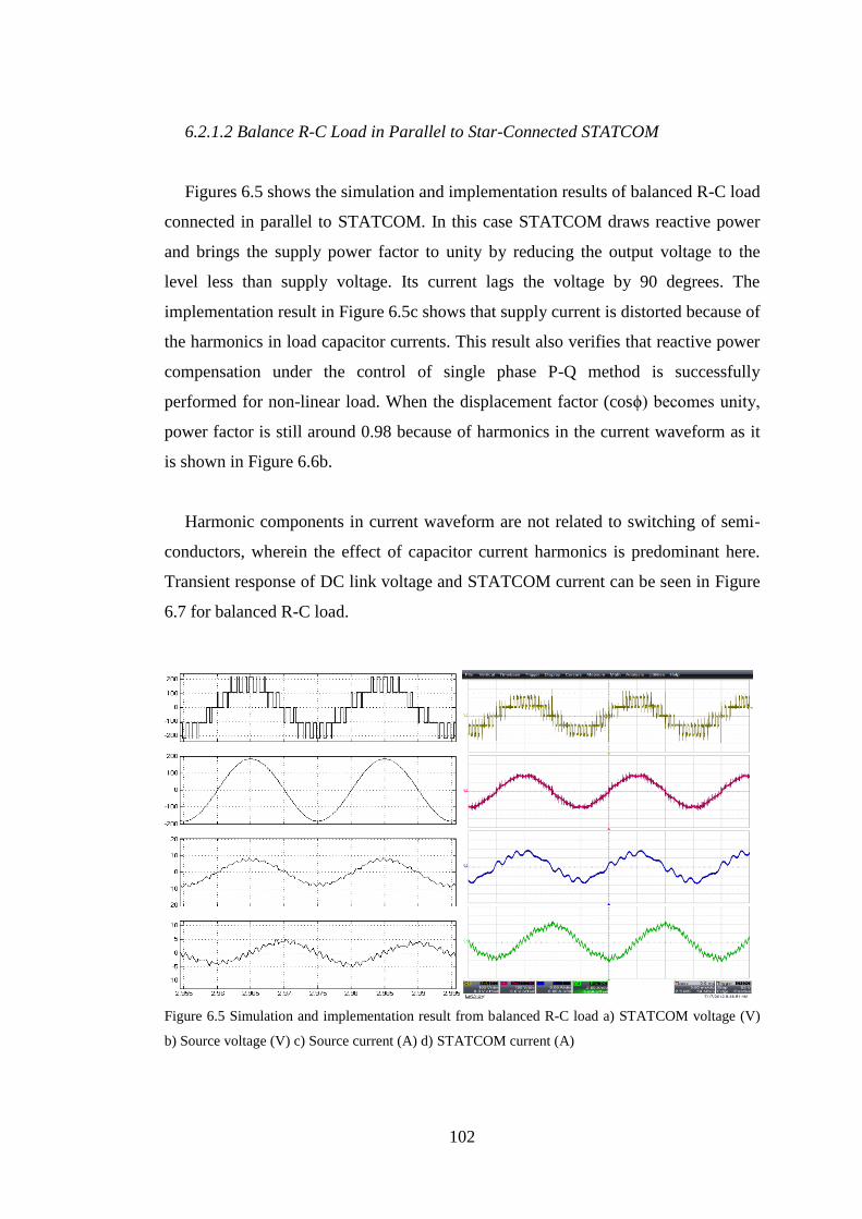
102
6.2.1.2 Balance R-C Load in Parallel to Star-Connected STATCOM
Figures 6.5 shows the simulation and implementation results of balanced R-C load
connected in parallel to STATCOM. In this case STATCOM draws reactive power
and brings the supply power factor to unity by reducing the output voltage to the
level less than supply voltage. Its current lags the voltage by 90 degrees. The
implementation result in Figure 6.5c shows that supply current is distorted because of
the harmonics in load capacitor currents. This result also verifies that reactive power
compensation under the control of single phase P-Q method is successfully
performed for non-linear load. When the displacement factor (cosϕ) becomes unity,
power factor is still around 0.98 because of harmonics in the current waveform as it
is shown in Figure 6.6b.
Harmonic components in current waveform are not related to switching of semi-
conductors, wherein the effect of capacitor current harmonics is predominant here.
Transient response of DC link voltage and STATCOM current can be seen in Figure
6.7 for balanced R-C load.
Figure 6.5 Simulation and implementation result from balanced R-C load a) STATCOM voltage (V)
b) Source voltage (V) c) Source current (A) d) STATCOM current (A)
103
Figure 6.6 Power & Energy measurement a) STATCOM is disconnected b) STATCOM is
connected c) Harmonic content of source current
Figure 6.7 Transient response of STATCOM with balanced R-C load a) DC link voltage (V) b)
STATCOM voltage (V) c) Source current (A) d) STATCOM current (A)
6.2.1.3 Balance R Load in Parallel to Star-Connected STATCOM
Figure 6.8 shows the simulation and implementation results of balanced resistive
R load. Its parameters are given in Table 6.1. In this case STATCOM does not draw
or generate reactive power and power factor in supply continues to remain unity.
STATCOM output voltage is kept equal to the supply voltage to ensure that there is
no reactive power flow on system however small amount active power must be
drawn from supply in order to keep voltage level of capacitor at predefined value.
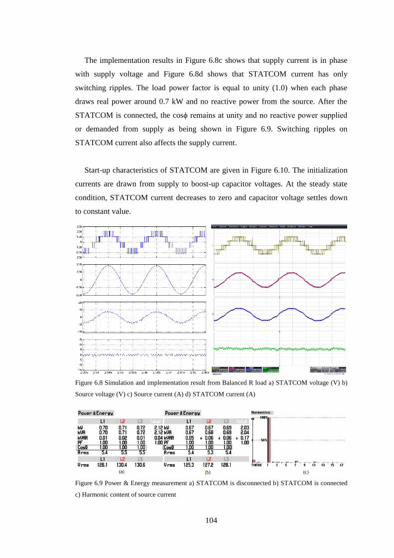
104
The implementation results in Figure 6.8c shows that supply current is in phase
with supply voltage and Figure 6.8d shows that STATCOM current has only
switching ripples. The load power factor is equal to unity (1.0) when each phase
draws real power around 0.7 kW and no reactive power from the source. After the
STATCOM is connected, the cosϕ remains at unity and no reactive power supplied
or demanded from supply as being shown in Figure 6.9. Switching ripples on
STATCOM current also affects the supply current.
Start-up characteristics of STATCOM are given in Figure 6.10. The initialization
currents are drawn from supply to boost-up capacitor voltages. At the steady state
condition, STATCOM current decreases to zero and capacitor voltage settles down
to constant value.
Figure 6.8 Simulation and implementation result from Balanced R load a) STATCOM voltage (V) b)
Source voltage (V) c) Source current (A) d) STATCOM current (A)
Figure 6.9 Power & Energy measurement a) STATCOM is disconnected b) STATCOM is connected
c) Harmonic content of source current
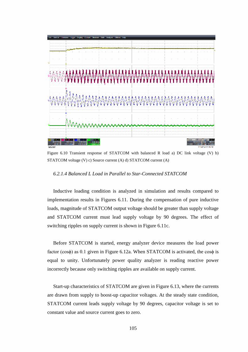
105
Figure 6.10 Transient response of STATCOM with balanced R load a) DC link voltage (V) b)
STATCOM voltage (V) c) Source current (A) d) STATCOM current (A)
6.2.1.4 Balanced L Load in Parallel to Star-Connected STATCOM
Inductive loading condition is analyzed in simulation and results compared to
implementation results in Figures 6.11. During the compensation of pure inductive
loads, magnitude of STATCOM output voltage should be greater than supply voltage
and STATCOM current must lead supply voltage by 90 degrees. The effect of
switching ripples on supply current is shown in Figure 6.11c.
Before STATCOM is started, energy analyzer device measures the load power
factor (cosϕ) as 0.1 given in Figure 6.12a. When STATCOM is activated, the cosϕ is
equal to unity. Unfortunately power quality analyzer is reading reactive power
incorrectly because only switching ripples are available on supply current.
Start-up characteristics of STATCOM are given in Figure 6.13, where the currents
are drawn from supply to boost-up capacitor voltages. At the steady state condition,
STATCOM current leads supply voltage by 90 degrees, capacitor voltage is set to
constant value and source current goes to zero.

106
Figure 6.11 Simulation and implementation result from balanced L load a) STATCOM voltage (V) b)
Source voltage (V) c) Source current (A) d) STATCOM current (A)
Figure 6.12 Power & Energy measurement a) STATCOM is disconnected b) STATCOM is connected
c) Harmonic content of source current
Figure 6.13 Transient response of STATCOM with balanced L load a) DC link voltage (V) b)
STATCOM voltage (V) c) Source current (A) d) STATCOM current (A)
107
6.2.1.5 Balanced C Load in Parallel to Star-Connected STATCOM
Another loading condition that is confirmed simulation and implementation works
are the capacitive loading as shown in the Figures 6.14. Magnitude of STATCOM
voltage becomes less than supply voltage for the compensation of pure capacitive
load and STATCOM current must lag supply voltage by 90 degrees. The
compensated supply current has only switching ripples as it is clearly observed in
Figure 6.14c
0.35 KVAR reactive powers are produced by capacitive load with zero power
factor as being shown in Figure 6.15. When the STATCOM is activated cosϕ
becomes unity. However power quality analyzer is reading reactive power
incorrectly because there is only switching ripple on supply current as it can be seen
on Figure 6.14c.
Start-up characteristics of STATCOM under balanced C load are given in Figure
6.16. The currents are drawn from supply to boost-up capacitor voltages. At the
steady state condition, STATCOM current lags supply voltage by 90 degrees,
capacitor voltage is set to constant value and source current decreases to zero.
Figure 6.14 Simulation and implementation result from balanced C load a) STATCOM voltage (V) b)
Source voltage (V) c) Source current (A) d) STATCOM current (A)

108
Figure 6.15 Power & Energy measurement a) STATCOM is disconnected b) STATCOM is connected
c) Harmonic content of source current
Figure 6.16 Transient response of STATCOM with balanced C load a) DC link voltage (V) b)
STATCOM voltage (V) c) Source current (A) d) STATCOM current (A)
6.2.2 Unbalanced Load in Parallel to Star-Connected STATCOM
Five different balanced loading conditions are compensated successfully by three-
phase star-connected STATCOM. Single phase P-Q algorithm can calculate reactive
power of each phase separately owing to the neutral connection that regardless of the
load balanced or unbalanced.
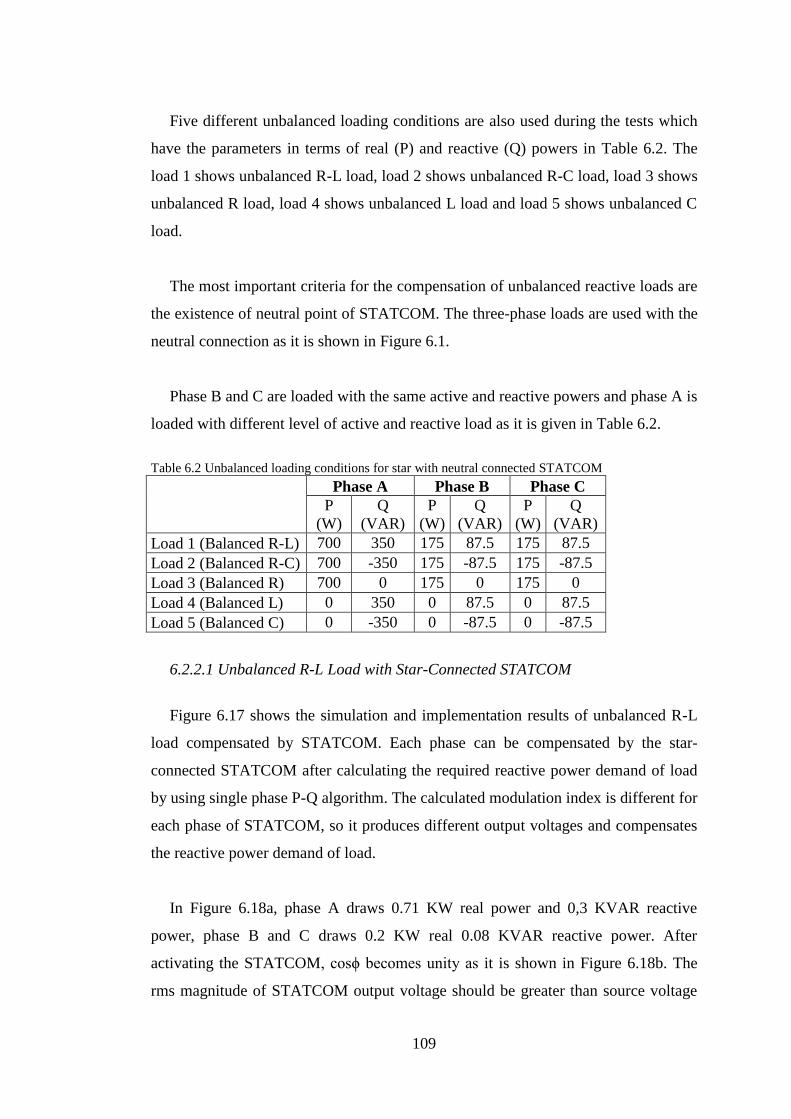
109
Five different unbalanced loading conditions are also used during the tests which
have the parameters in terms of real (P) and reactive (Q) powers in Table 6.2. The
load 1 shows unbalanced R-L load, load 2 shows unbalanced R-C load, load 3 shows
unbalanced R load, load 4 shows unbalanced L load and load 5 shows unbalanced C
load.
The most important criteria for the compensation of unbalanced reactive loads are
the existence of neutral point of STATCOM. The three-phase loads are used with the
neutral connection as it is shown in Figure 6.1.
Phase B and C are loaded with the same active and reactive powers and phase A is
loaded with different level of active and reactive load as it is given in Table 6.2.
Table 6.2 Unbalanced loading conditions for star with neutral connected STATCOM
Phase A Phase B Phase C
P
(W)
Q
(VAR)
P
(W)
Q
(VAR)
P
(W)
Q
(VAR)
Load 1 (Balanced R-L) 700 350 175 87.5 175 87.5
Load 2 (Balanced R-C) 700 -350 175 -87.5 175 -87.5
Load 3 (Balanced R) 700 0 175 0 175 0
Load 4 (Balanced L) 0 350 0 87.5 0 87.5
Load 5 (Balanced C) 0 -350 0 -87.5 0 -87.5
6.2.2.1 Unbalanced R-L Load with Star-Connected STATCOM
Figure 6.17 shows the simulation and implementation results of unbalanced R-L
load compensated by STATCOM. Each phase can be compensated by the star-
connected STATCOM after calculating the required reactive power demand of load
by using single phase P-Q algorithm. The calculated modulation index is different for
each phase of STATCOM, so it produces different output voltages and compensates
the reactive power demand of load.
In Figure 6.18a, phase A draws 0.71 KW real power and 0,3 KVAR reactive
power, phase B and C draws 0.2 KW real 0.08 KVAR reactive power. After
activating the STATCOM, cosϕ becomes unity as it is shown in Figure 6.18b. The
rms magnitude of STATCOM output voltage should be greater than source voltage
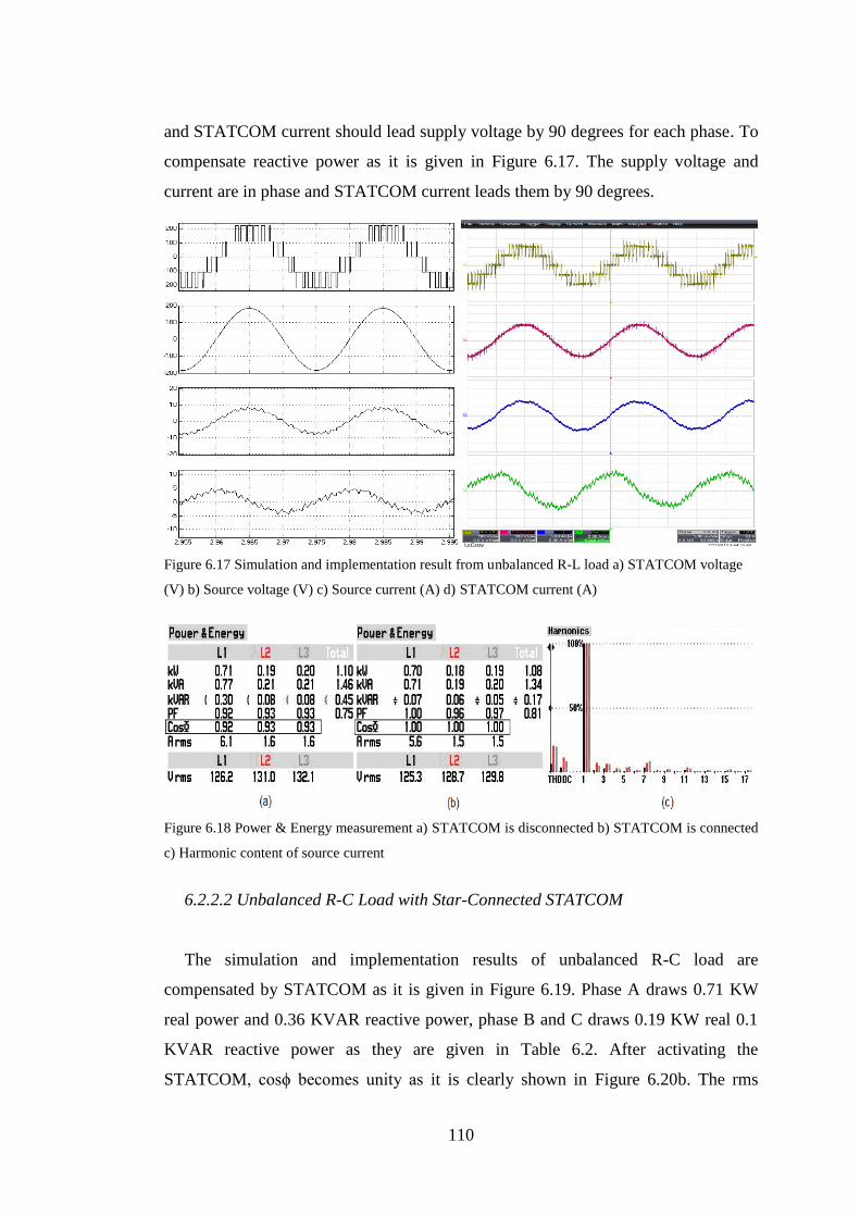
110
and STATCOM current should lead supply voltage by 90 degrees for each phase. To
compensate reactive power as it is given in Figure 6.17. The supply voltage and
current are in phase and STATCOM current leads them by 90 degrees.
Figure 6.17 Simulation and implementation result from unbalanced R-L load a) STATCOM voltage
(V) b) Source voltage (V) c) Source current (A) d) STATCOM current (A)
Figure 6.18 Power & Energy measurement a) STATCOM is disconnected b) STATCOM is connected
c) Harmonic content of source current
6.2.2.2 Unbalanced R-C Load with Star-Connected STATCOM
The simulation and implementation results of unbalanced R-C load are
compensated by STATCOM as it is given in Figure 6.19. Phase A draws 0.71 KW
real power and 0.36 KVAR reactive power, phase B and C draws 0.19 KW real 0.1
KVAR reactive power as they are given in Table 6.2. After activating the
STATCOM, cosϕ becomes unity as it is clearly shown in Figure 6.20b. The rms

111
magnitude of STATCOM output voltage is lower than source voltage and
STATCOM current lags supply voltage by 90 degrees for each phase as it is
observed from Figure 6.19. The supply voltage and current are in phase and
STATCOM current lags them by 90 degrees.
Figure 6.19 Simulation and implementation result from unbalanced R-C load a) STATCOM voltage
(V) b) Source voltage (V) c) Source current (A) d) STATCOM current (A)
Figure 6.20 Power & Energy measurement a) STATCOM is disconnected b) STATCOM is connected
c) Harmonic content of source current
6.2.2.3 Unbalanced R Load with Star-Connected STATCOM
Figure 6.21 shows the simulation and implementation results of unbalanced R
load and its parameters are given in Table 6.2. The phase A draws 0.69 KW reel
power, phase B and C draw 0.19 KW reel power as it is shown in Figure 6.22a. In
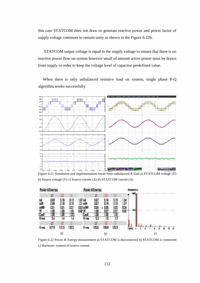
112
this case STATCOM does not draw or generate reactive power and power factor of
supply voltage continues to remain unity as shown in the Figure 6.22b.
STATCOM output voltage is equal to the supply voltage to ensure that there is no
reactive power flow on system however small of amount active power must be drawn
from supply in order to keep the voltage level of capacitor predefined value.
When there is only unbalanced resistive load on system, single phase P-Q
algorithm works successfully.
Figure 6.21 Simulation and implementation result from unbalanced R load a) STATCOM voltage (V)
b) Source voltage (V) c) Source current (A) d) STATCOM current (A)
Figure 6.22 Power & Energy measurement a) STATCOM is disconnected b) STATCOM is connected
c) Harmonic content of source current
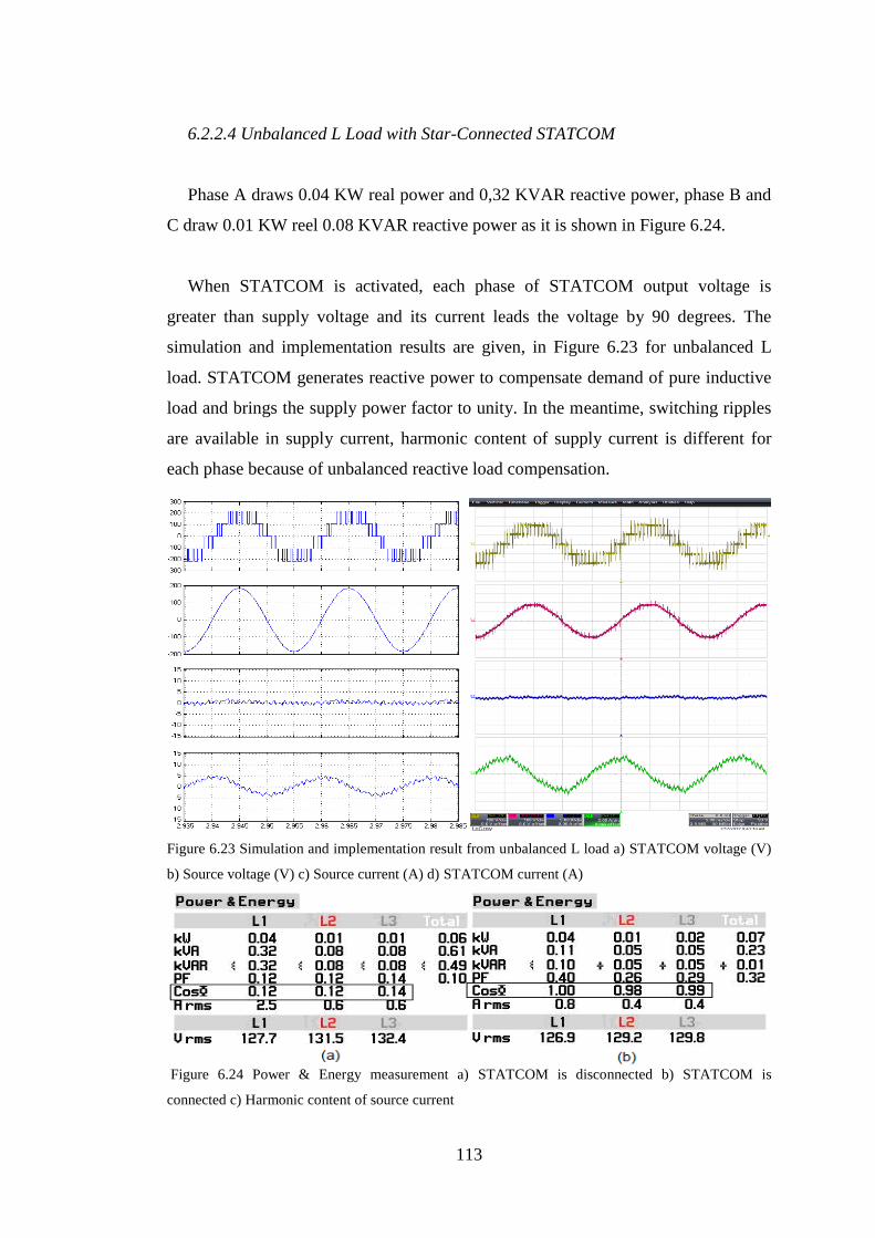
113
6.2.2.4 Unbalanced L Load with Star-Connected STATCOM
Phase A draws 0.04 KW real power and 0,32 KVAR reactive power, phase B and
C draw 0.01 KW reel 0.08 KVAR reactive power as it is shown in Figure 6.24.
When STATCOM is activated, each phase of STATCOM output voltage is
greater than supply voltage and its current leads the voltage by 90 degrees. The
simulation and implementation results are given, in Figure 6.23 for unbalanced L
load. STATCOM generates reactive power to compensate demand of pure inductive
load and brings the supply power factor to unity. In the meantime, switching ripples
are available in supply current, harmonic content of supply current is different for
each phase because of unbalanced reactive load compensation.
Figure 6.23 Simulation and implementation result from unbalanced L load a) STATCOM voltage (V)
b) Source voltage (V) c) Source current (A) d) STATCOM current (A)
Figure 6.24 Power & Energy measurement a) STATCOM is disconnected b) STATCOM is
connected c) Harmonic content of source current
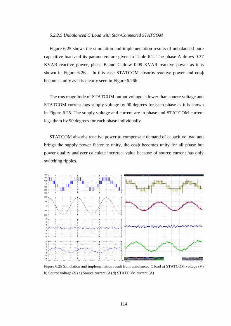
114
6.2.2.5 Unbalanced C Load with Star-Connected STATCOM
Figure 6.25 shows the simulation and implementation results of unbalanced pure
capacitive load and its parameters are given in Table 6.2. The phase A draws 0.37
KVAR reactive power, phase B and C draw 0.09 KVAR reactive power as it is
shown in Figure 6.26a. In this case STATCOM absorbs reactive power and cosϕ
becomes unity as it is clearly seen in Figure 6.26b.
The rms magnitude of STATCOM output voltage is lower than source voltage and
STATCOM current lags supply voltage by 90 degrees for each phase as it is shown
in Figure 6.25. The supply voltage and current are in phase and STATCOM current
lags them by 90 degrees for each phase individually.
STATCOM absorbs reactive power to compensate demand of capacitive load and
brings the supply power factor to unity, the cosϕ becomes unity for all phase but
power quality analyzer calculate incorrect value because of source current has only
switching ripples.
Figure 6.25 Simulation and implementation result from unbalanced C load a) STATCOM voltage (V)
b) Source voltage (V) c) Source current (A) d) STATCOM current (A)

115
Figure 6.26 Power & Energy measurement a) STATCOM is disconnected b) STATCOM is connected
c) Harmonic content of source current
6.2.3 Evaluation of Star-Connected Converter as STATCOM
A proposed converter that has reduced number of switches is used as three-phase
star-connected STATCOM. The result of the simulation and implementation work
shows that this converter has all the features of conventional H-bridge converter.
Besides, it is verified that level shifted carrier based SPWM, capacitor voltage
balancing technique and control of single phase instantaneous reactive power method
are successfully implemented in the program on floating point DSP. The results show
that the reactive power control method and proposed converter can be used for
balanced load compensation if star connection is performed with neutral line. If the
neutral point of load is available, then each phase can be compensated independently.
In Table 6.3, proposed STATCOM structure is examined according to THD
performance under loaded conditions. The resistive load is a linear load however
inductance is somehow affected from saturation (level of current) and capacitive load
can show non-linear effect with source parameters and harmonics generated by the
STATCOM. The high THD value in the R-C loading in experimental work is due to
capacitive load itself.
The energy analyzer Fluke 434 can measure up to 17th
harmonics in three-phase
harmonics and THD measurements mode. For this reason, the THD values obtained
in the simulation study are slightly higher than the implementation results.
Matlab/Simulink THD measurement tool uses the entire frequency spectrum.
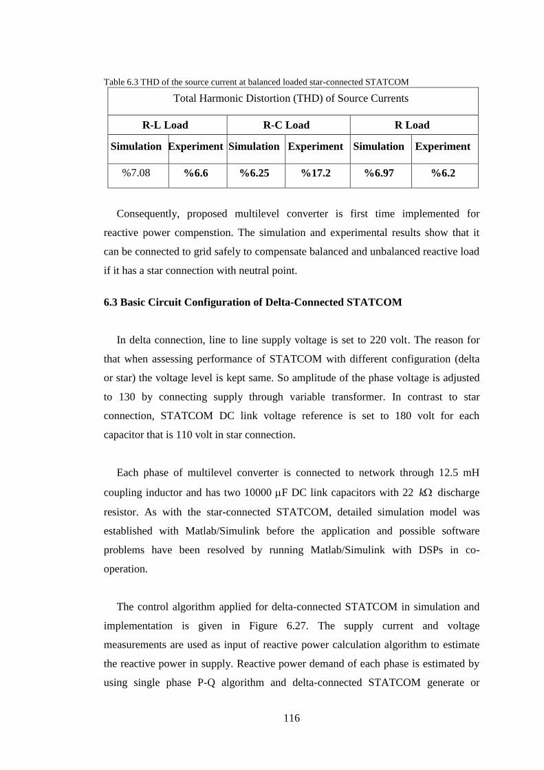
116
Table 6.3 THD of the source current at balanced loaded star-connected STATCOM
Total Harmonic Distortion (THD) of Source Currents
R-L Load R-C Load R Load
Simulation Experiment Simulation Experiment Simulation Experiment
%7.08 %6.6 %6.25 %17.2 %6.97 %6.2
Consequently, proposed multilevel converter is first time implemented for
reactive power compenstion. The simulation and experimental results show that it
can be connected to grid safely to compensate balanced and unbalanced reactive load
if it has a star connection with neutral point.
6.3 Basic Circuit Configuration of Delta-Connected STATCOM
In delta connection, line to line supply voltage is set to 220 volt. The reason for
that when assessing performance of STATCOM with different configuration (delta
or star) the voltage level is kept same. So amplitude of the phase voltage is adjusted
to 130 by connecting supply through variable transformer. In contrast to star
connection, STATCOM DC link voltage reference is set to 180 volt for each
capacitor that is 110 volt in star connection.
Each phase of multilevel converter is connected to network through 12.5 mH
coupling inductor and has two 10000 F DC link capacitors with 22 k discharge
resistor. As with the star-connected STATCOM, detailed simulation model was
established with Matlab/Simulink before the application and possible software
problems have been resolved by running Matlab/Simulink with DSPs in co-
operation.
The control algorithm applied for delta-connected STATCOM in simulation and
implementation is given in Figure 6.27. The supply current and voltage
measurements are used as input of reactive power calculation algorithm to estimate
the reactive power in supply. Reactive power demand of each phase is estimated by
using single phase P-Q algorithm and delta-connected STATCOM generate or

117
absorb it by changing modulation index. PI controller that controls the modulation
index, allows compensating reactive power on three-phase.
The main differences between applied control algorithm in delta-connected
STATCOM and star-connected STATCOM are line to line voltages read for software
and neutral connections of load. STATCOM has no connection to the neutral point of
supply. Modulation index is calculated by using the output of reactive power
calculation algorithm. The PI controller output is multiplied by triangular signal and
carrier signal is obtained. In the mean time, the PLL circuit produces reference
sinusoidal signal by using line to line supply voltages. Reference sinusoidal voltage
has a phase shift with respect to the corresponding supply line to line voltage. The
reason for this is to control real power flows to balance the converter power loss and
regulating the DC link capacitor voltages with the help of PI controllers as being
shown in the block diagram of the system in Figure 6.27. Besides the giving phase
shift in reference signal, swapping algorithm is also applied to balance DC link
capacitor voltages by changing phase angle in every period. Finally, IGBT gate
signals are obtained by comparing reference sinusoidal signal with triangular carrier
signal.
Figure 6.27 Control schematic of delta-connected STATCOM
118
According to the simulation and implementation results obtained, while the
unbalanced reactive power is compensated, it is observed that the real power flow
through each phase has changed. This is not exactly a load balancing; it is a situation
that is created by reactive power estimated with phase voltage and current.
Firstly, balanced loading conditions for delta-connected STATCOM are analyzed
in simulation and it is implemented. In the next stage, the same study is repeated for
unbalanced loads.
Three phase supply voltages are as follows;
)sin(. vVa (6.1)
)3
2sin(.
vVb (6.2)
)3
2sin(.
vVc
(6.3)
The line to line voltage can be obtained from phase voltages;
)6
sin(..3
vVab (6.4)
)2
sin(..3
vVbc (6.5)
)6
5sin(..3
vVca
(6.6)
STATCOM current leads line to line supply voltages by 90 degrees that is assured
by coupling inductance of STATCOM in order to compensate the inductive load;
)3
2sin(.
iI ab (6.7)
)sin(. iIbc (6.8)
)3
2sin(.
iI ca (6.9)
119
Phase current A can be found by subtracting line current as given Equation (6.10).
If substituted line current in Equation (6.11), phase current A is found as leading
phase voltage 90 degrees.
caaba III (6.10)
)3
2sin(.)
3
2sin(.
iiI a
(6.11)
)2
sin(..3
iI a (6.12)
Phase current B can also be found as below,
abbcb III (6.13)
)3
2sin(.)sin(.
iiIb
(6.14)
)6
sin(..3
iIb (6.15)
Phase current C can also be found as follows,
bccac III (6.16)
)sin(.)3
2sin(.
iiIc (6.17)
)6
5sin(..3
iI c
(6.18)
If the capacitive load is compensated by STATCOM, source current will be as
follows;
)2
sin(..3
iI a (6.19)
)6
5sin(..3
iIb (6.20)
)6
sin(..3
iI c (6.21)

120
The analysis shows that, all phase currents lead or lag phase voltages by 90
degrees and the reactive power can be compensated by following the line to line
voltages.
6.3.1 Balanced Loading Condition for Delta-Connected STATCOM
Five different balanced loading conditions used during the tests are given in terms
of real (P) and reactive (Q) powers in Table 6.4. The load 1 shows balanced R-L
load, load 2 shows balanced R-C load, load 3 shows balanced R load, load 4 shows
balanced L load and load 5 shows balanced C load.
Table 6.4 Balanced loading conditions for delta-connected STATCOM
Phase A Phase B Phase C
P
(W)
Q
(VAR)
P
(W)
Q
(VAR)
P
(W)
Q
(VAR)
Load 1 (Balanced R-L) 700 350 700 350 700 350
Load 2 (Balanced R-C) 700 -350 700 -350 700 -350
Load 3 (Balanced R) 700 0 700 0 700 0
Load 4 (Balanced L) 0 350 0 350 0 350
Load 5 (Balanced C) 0 -350 0 -350 0 -350
6.3.1.1 Balanced R-L load on Delta-Connected STATCOM
The simulation and implementation results of balanced R-L load are given in
Figures 6.28. The rms magnitude of STATCOM output voltage is greater than source
voltage and STATCOM current leads voltage by 90 degrees. It generates the reactive
power and compensates the demand of inductive load. The load power factor is 0.92
and real power demand of around 0.73 kW and reactive power demand is around
0.31 KVAR as it is shown in Figure 6.29a. After activating the STATCOM, cosϕ
becomes unity and reactive power supplied from the source is going to zero as it can
be observed from Figure 6.29b. The effect of switching harmonics can be seen on
supply current in Figure 6.29c.
Start-up characteristics of delta-connected STATCOM under R-L loading
conditions are seen in Figure 6.30. The starting currents are drawn from supply to
boost-up capacitor voltages. At the steady state condition, STATCOM current goes
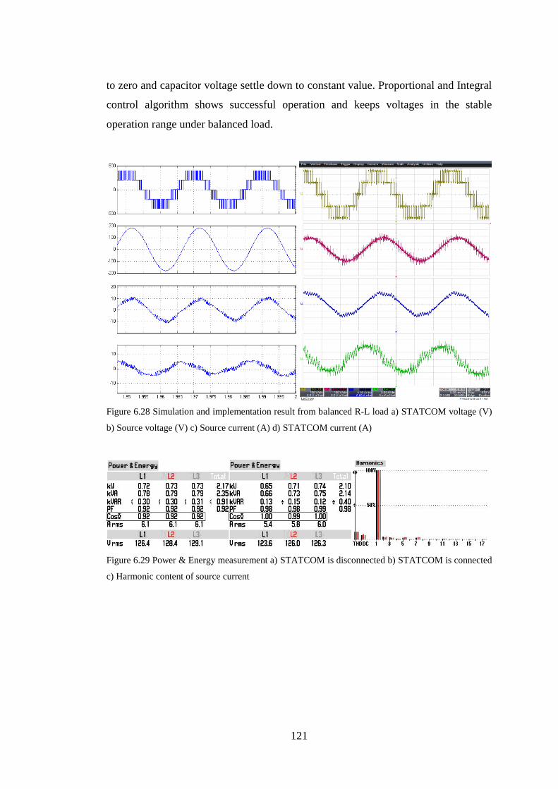
121
to zero and capacitor voltage settle down to constant value. Proportional and Integral
control algorithm shows successful operation and keeps voltages in the stable
operation range under balanced load.
Figure 6.28 Simulation and implementation result from balanced R-L load a) STATCOM voltage (V)
b) Source voltage (V) c) Source current (A) d) STATCOM current (A)
Figure 6.29 Power & Energy measurement a) STATCOM is disconnected b) STATCOM is connected
c) Harmonic content of source current
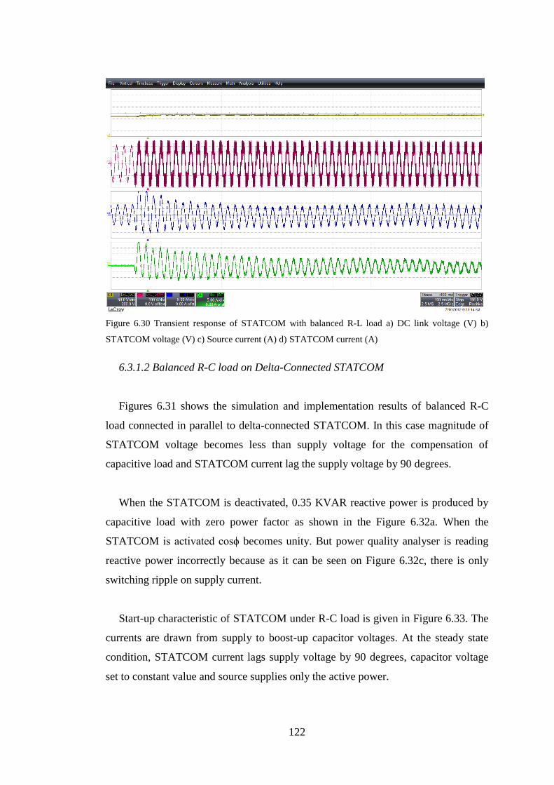
122
Figure 6.30 Transient response of STATCOM with balanced R-L load a) DC link voltage (V) b)
STATCOM voltage (V) c) Source current (A) d) STATCOM current (A)
6.3.1.2 Balanced R-C load on Delta-Connected STATCOM
Figures 6.31 shows the simulation and implementation results of balanced R-C
load connected in parallel to delta-connected STATCOM. In this case magnitude of
STATCOM voltage becomes less than supply voltage for the compensation of
capacitive load and STATCOM current lag the supply voltage by 90 degrees.
When the STATCOM is deactivated, 0.35 KVAR reactive power is produced by
capacitive load with zero power factor as shown in the Figure 6.32a. When the
STATCOM is activated cosϕ becomes unity. But power quality analyser is reading
reactive power incorrectly because as it can be seen on Figure 6.32c, there is only
switching ripple on supply current.
Start-up characteristic of STATCOM under R-C load is given in Figure 6.33. The
currents are drawn from supply to boost-up capacitor voltages. At the steady state
condition, STATCOM current lags supply voltage by 90 degrees, capacitor voltage
set to constant value and source supplies only the active power.
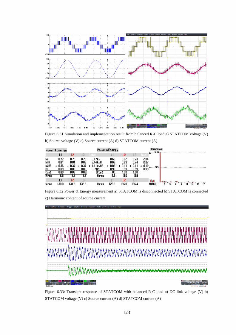
123
Figure 6.31 Simulation and implementation result from balanced R-C load a) STATCOM voltage (V)
b) Source voltage (V) c) Source current (A) d) STATCOM current (A)
Figure 6.32 Power & Energy measurement a) STATCOM is disconnected b) STATCOM is connected
c) Harmonic content of source current
Figure 6.33: Transient response of STATCOM with balanced R-C load a) DC link voltage (V) b)
STATCOM voltage (V) c) Source current (A) d) STATCOM current (A)
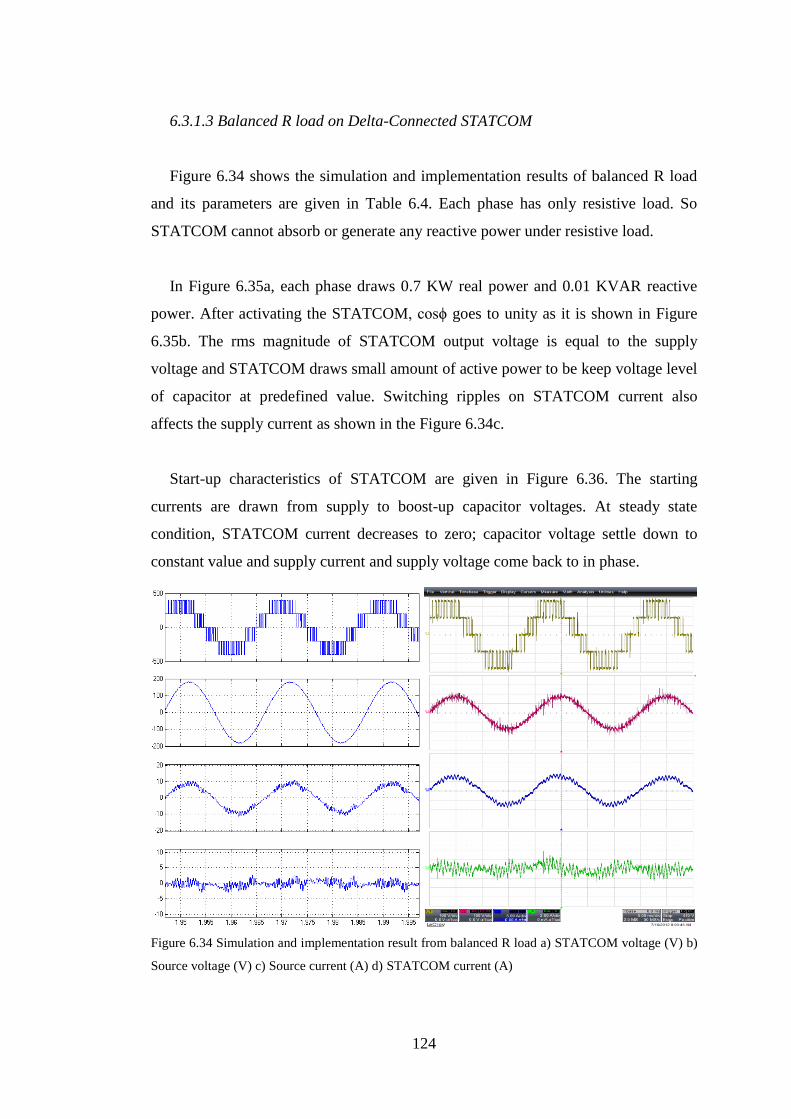
124
6.3.1.3 Balanced R load on Delta-Connected STATCOM
Figure 6.34 shows the simulation and implementation results of balanced R load
and its parameters are given in Table 6.4. Each phase has only resistive load. So
STATCOM cannot absorb or generate any reactive power under resistive load.
In Figure 6.35a, each phase draws 0.7 KW real power and 0.01 KVAR reactive
power. After activating the STATCOM, cosϕ goes to unity as it is shown in Figure
6.35b. The rms magnitude of STATCOM output voltage is equal to the supply
voltage and STATCOM draws small amount of active power to be keep voltage level
of capacitor at predefined value. Switching ripples on STATCOM current also
affects the supply current as shown in the Figure 6.34c.
Start-up characteristics of STATCOM are given in Figure 6.36. The starting
currents are drawn from supply to boost-up capacitor voltages. At steady state
condition, STATCOM current decreases to zero; capacitor voltage settle down to
constant value and supply current and supply voltage come back to in phase.
Figure 6.34 Simulation and implementation result from balanced R load a) STATCOM voltage (V) b)
Source voltage (V) c) Source current (A) d) STATCOM current (A)
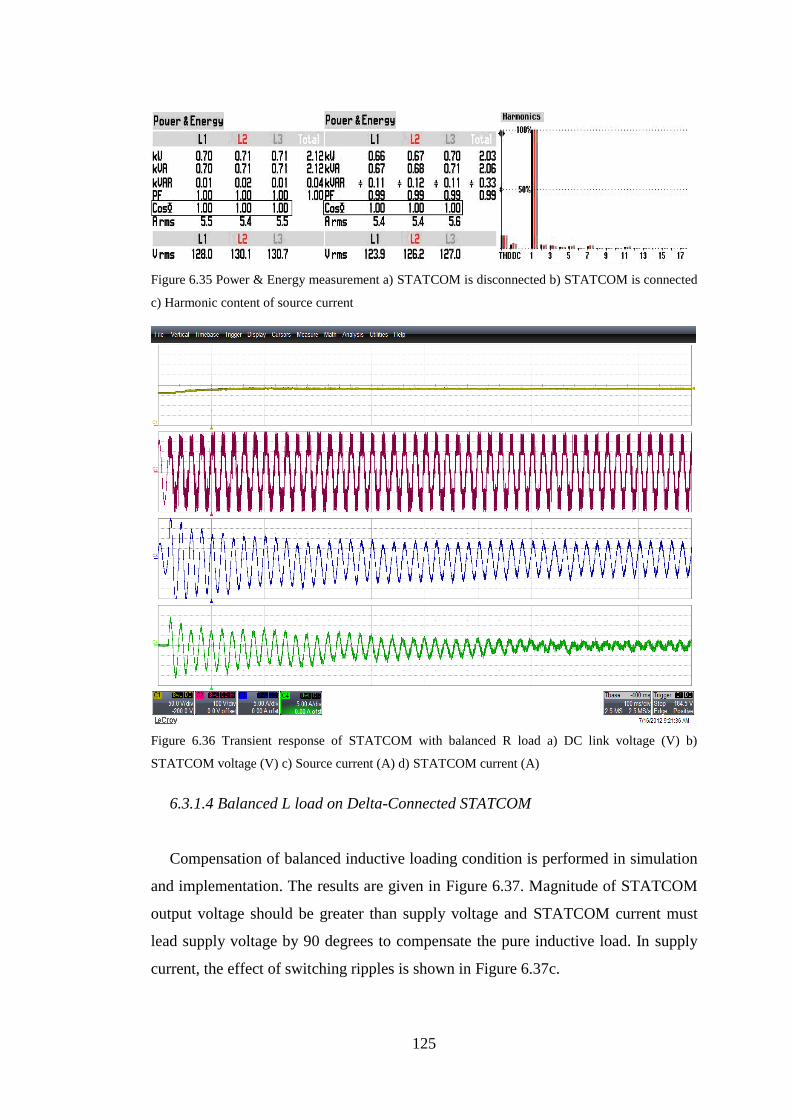
125
Figure 6.35 Power & Energy measurement a) STATCOM is disconnected b) STATCOM is connected
c) Harmonic content of source current
Figure 6.36 Transient response of STATCOM with balanced R load a) DC link voltage (V) b)
STATCOM voltage (V) c) Source current (A) d) STATCOM current (A)
6.3.1.4 Balanced L load on Delta-Connected STATCOM
Compensation of balanced inductive loading condition is performed in simulation
and implementation. The results are given in Figure 6.37. Magnitude of STATCOM
output voltage should be greater than supply voltage and STATCOM current must
lead supply voltage by 90 degrees to compensate the pure inductive load. In supply
current, the effect of switching ripples is shown in Figure 6.37c.
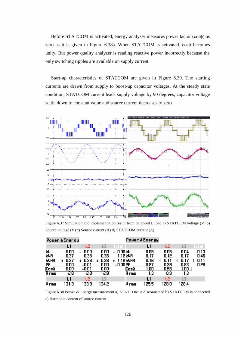
126
Before STATCOM is activated, energy analyzer measures power factor (cosϕ) as
zero as it is given in Figure 6.38a. When STATCOM is activated, cosϕ becomes
unity. But power quality analyzer is reading reactive power incorrectly because the
only switching ripples are available on supply current.
Start-up characteristics of STATCOM are given in Figure 6.39. The starting
currents are drawn from supply to boost-up capacitor voltages. At the steady state
condition, STATCOM current leads supply voltage by 90 degrees, capacitor voltage
settle down to constant value and source current decreases to zero.
Figure 6.37 Simulation and implementation result from balanced L load a) STATCOM voltage (V) b)
Source voltage (V) c) Source current (A) d) STATCOM current (A)
Figure 6.38 Power & Energy measurement a) STATCOM is disconnected b) STATCOM is connected
c) Harmonic content of source current
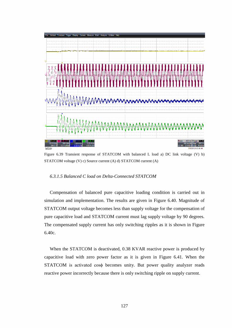
127
Figure 6.39 Transient response of STATCOM with balanced L load a) DC link voltage (V) b)
STATCOM voltage (V) c) Source current (A) d) STATCOM current (A)
6.3.1.5 Balanced C load on Delta-Connected STATCOM
Compensation of balanced pure capacitive loading condition is carried out in
simulation and implementation. The results are given in Figure 6.40. Magnitude of
STATCOM output voltage becomes less than supply voltage for the compensation of
pure capacitive load and STATCOM current must lag supply voltage by 90 degrees.
The compensated supply current has only switching ripples as it is shown in Figure
6.40c.
When the STATCOM is deactivated, 0.38 KVAR reactive power is produced by
capacitive load with zero power factor as it is given in Figure 6.41. When the
STATCOM is activated cosϕ becomes unity. But power quality analyzer reads
reactive power incorrectly because there is only switching ripple on supply current.
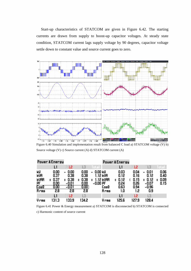
128
Start-up characteristics of STATCOM are given in Figure 6.42. The starting
currents are drawn from supply to boost-up capacitor voltages. At steady state
condition, STATCOM current lags supply voltage by 90 degrees, capacitor voltage
settle down to constant value and source current goes to zero.
Figure 6.40 Simulation and implementation result from balanced C load a) STATCOM voltage (V) b)
Source voltage (V) c) Source current (A) d) STATCOM current (A)
Figure 6.41 Power & Energy measurement a) STATCOM is disconnected b) STATCOM is connected
c) Harmonic content of source current

129
Figure 6.42 Transient response of STATCOM with balanced C load a) DC link voltage (V) b)
STATCOM voltage (V) c) Source current (A) d) STATCOM current (A)
6.3.2 Unbalanced Loading Conditions for Delta-Connected STATCOM
Five different unbalanced loading conditions are compensated successfully by
three-phase delta-connected STATCOM. The method uses single-phase PQ in delta-
connected STATCOM. It estimates the required reactive power for compensation.
Five different unbalanced loading conditions are used during the tests. Their
values are given in terms of real (P) and reactive (Q) powers in Table 6.5. The load 1
shows unbalanced R-L load, load 2 shows unbalanced R-C load, load 3 shows
unbalanced R load, load 4 shows unbalanced L load and load 5 shows unbalanced C
load.
Table 6.5 Unbalanced loading conditions for delta-connected STATCOM
Phase A Phase B Phase C
P
(W)
Q
(VAR)
P
(W)
Q
(VAR)
P
(W)
Q
(VAR)
Load 6 (Unbalanced R-L) 700 350 175 87.5 175 87.5
Load 7 (Unbalanced R-C) 700 -350 175 -87.5 175 -87.5
Load 8 (Unbalanced R) 700 0 700 0 700 0
Load 9 (Unbalanced L) 0 350 0 87.5 0 87.5
Load 10 (Unbalanced C) 0 -350 0 -87.5 0 -87.5
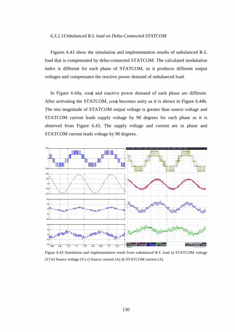
130
6.3.2.1Unbalanced R-L load on Delta-Connected STATCOM
Figures 6.43 show the simulation and implementation results of unbalanced R-L
load that is compensated by delta-connected STATCOM. The calculated modulation
index is different for each phase of STATCOM, so it produces different output
voltages and compensates the reactive power demand of unbalanced load.
In Figure 6.44a, cosϕ and reactive power demand of each phase are different.
After activating the STATCOM, cosϕ becomes unity as it is shown in Figure 6.44b.
The rms magnitude of STATCOM output voltage is greater than source voltage and
STATCOM current leads supply voltage by 90 degrees for each phase as it is
observed from Figure 6.43. The supply voltage and current are in phase and
STATCOM current leads voltage by 90 degrees.
Figure 6.43 Simulation and implementation result from unbalanced R-L load a) STATCOM voltage
(V) b) Source voltage (V) c) Source current (A) d) STATCOM current (A)
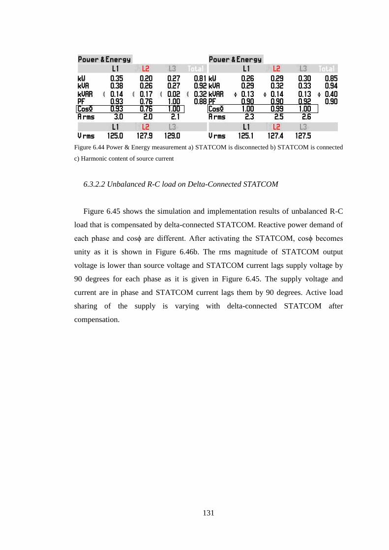
131
Figure 6.44 Power & Energy measurement a) STATCOM is disconnected b) STATCOM is connected
c) Harmonic content of source current
6.3.2.2 Unbalanced R-C load on Delta-Connected STATCOM
Figure 6.45 shows the simulation and implementation results of unbalanced R-C
load that is compensated by delta-connected STATCOM. Reactive power demand of
each phase and cosϕ are different. After activating the STATCOM, cosϕ becomes
unity as it is shown in Figure 6.46b. The rms magnitude of STATCOM output
voltage is lower than source voltage and STATCOM current lags supply voltage by
90 degrees for each phase as it is given in Figure 6.45. The supply voltage and
current are in phase and STATCOM current lags them by 90 degrees. Active load
sharing of the supply is varying with delta-connected STATCOM after
compensation.
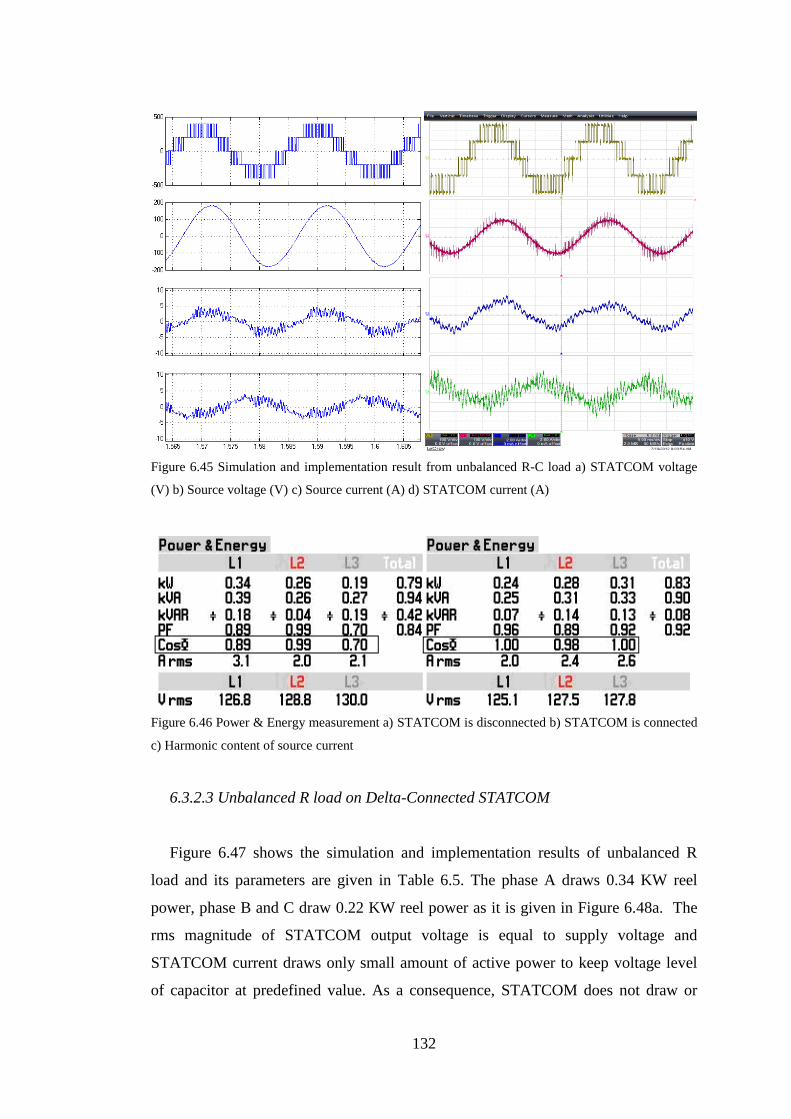
132
Figure 6.45 Simulation and implementation result from unbalanced R-C load a) STATCOM voltage
(V) b) Source voltage (V) c) Source current (A) d) STATCOM current (A)
Figure 6.46 Power & Energy measurement a) STATCOM is disconnected b) STATCOM is connected
c) Harmonic content of source current
6.3.2.3 Unbalanced R load on Delta-Connected STATCOM
Figure 6.47 shows the simulation and implementation results of unbalanced R
load and its parameters are given in Table 6.5. The phase A draws 0.34 KW reel
power, phase B and C draw 0.22 KW reel power as it is given in Figure 6.48a. The
rms magnitude of STATCOM output voltage is equal to supply voltage and
STATCOM current draws only small amount of active power to keep voltage level
of capacitor at predefined value. As a consequence, STATCOM does not draw or
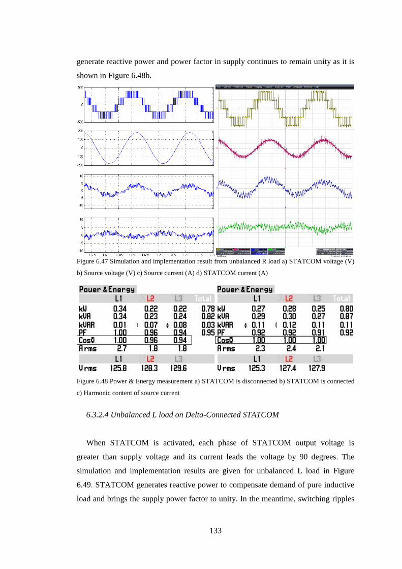
133
generate reactive power and power factor in supply continues to remain unity as it is
shown in Figure 6.48b.
Figure 6.47 Simulation and implementation result from unbalanced R load a) STATCOM voltage (V)
b) Source voltage (V) c) Source current (A) d) STATCOM current (A)
Figure 6.48 Power & Energy measurement a) STATCOM is disconnected b) STATCOM is connected
c) Harmonic content of source current
6.3.2.4 Unbalanced L load on Delta-Connected STATCOM
When STATCOM is activated, each phase of STATCOM output voltage is
greater than supply voltage and its current leads the voltage by 90 degrees. The
simulation and implementation results are given for unbalanced L load in Figure
6.49. STATCOM generates reactive power to compensate demand of pure inductive
load and brings the supply power factor to unity. In the meantime, switching ripples
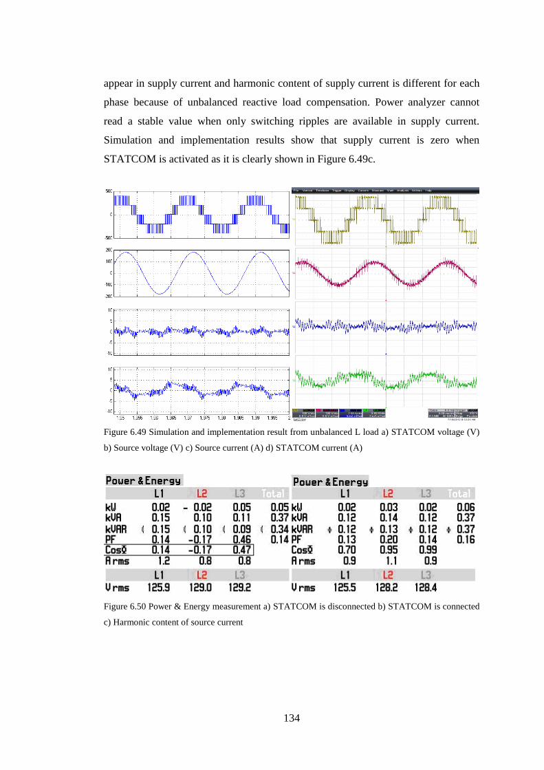
134
appear in supply current and harmonic content of supply current is different for each
phase because of unbalanced reactive load compensation. Power analyzer cannot
read a stable value when only switching ripples are available in supply current.
Simulation and implementation results show that supply current is zero when
STATCOM is activated as it is clearly shown in Figure 6.49c.
Figure 6.49 Simulation and implementation result from unbalanced L load a) STATCOM voltage (V)
b) Source voltage (V) c) Source current (A) d) STATCOM current (A)
Figure 6.50 Power & Energy measurement a) STATCOM is disconnected b) STATCOM is connected
c) Harmonic content of source current
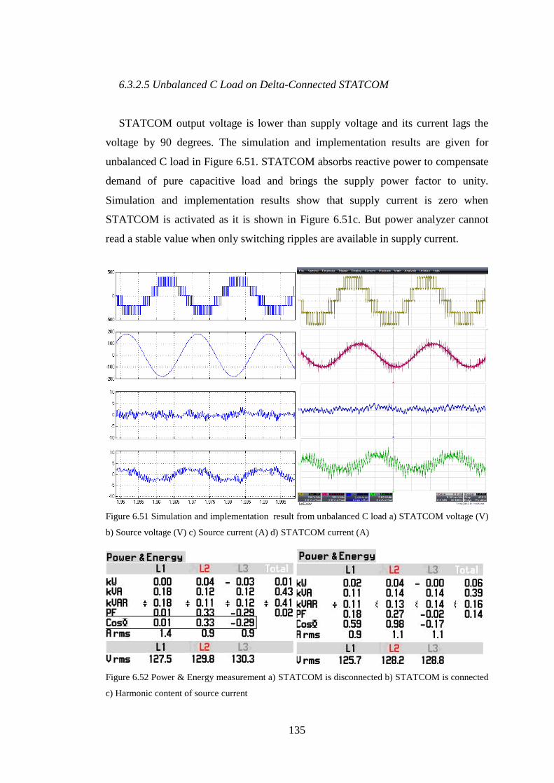
135
6.3.2.5 Unbalanced C Load on Delta-Connected STATCOM
STATCOM output voltage is lower than supply voltage and its current lags the
voltage by 90 degrees. The simulation and implementation results are given for
unbalanced C load in Figure 6.51. STATCOM absorbs reactive power to compensate
demand of pure capacitive load and brings the supply power factor to unity.
Simulation and implementation results show that supply current is zero when
STATCOM is activated as it is shown in Figure 6.51c. But power analyzer cannot
read a stable value when only switching ripples are available in supply current.
Figure 6.51 Simulation and implementation result from unbalanced C load a) STATCOM voltage (V)
b) Source voltage (V) c) Source current (A) d) STATCOM current (A)
Figure 6.52 Power & Energy measurement a) STATCOM is disconnected b) STATCOM is connected
c) Harmonic content of source current
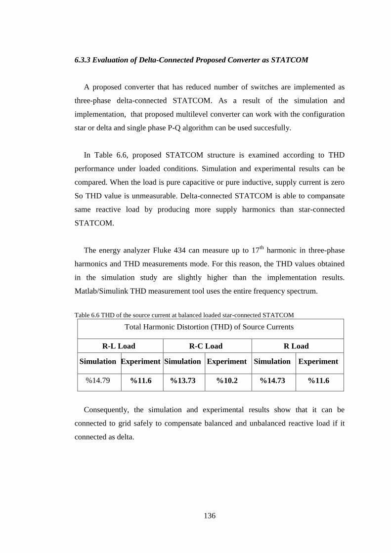
136
6.3.3 Evaluation of Delta-Connected Proposed Converter as STATCOM
A proposed converter that has reduced number of switches are implemented as
three-phase delta-connected STATCOM. As a result of the simulation and
implementation, that proposed multilevel converter can work with the configuration
star or delta and single phase P-Q algorithm can be used succesfully.
In Table 6.6, proposed STATCOM structure is examined according to THD
performance under loaded conditions. Simulation and experimental results can be
compared. When the load is pure capacitive or pure inductive, supply current is zero
So THD value is unmeasurable. Delta-connected STATCOM is able to compansate
same reactive load by producing more supply harmonics than star-connected
STATCOM.
The energy analyzer Fluke 434 can measure up to 17th
harmonic in three-phase
harmonics and THD measurements mode. For this reason, the THD values obtained
in the simulation study are slightly higher than the implementation results.
Matlab/Simulink THD measurement tool uses the entire frequency spectrum.
Table 6.6 THD of the source current at balanced loaded star-connected STATCOM
Total Harmonic Distortion (THD) of Source Currents
R-L Load R-C Load R Load
Simulation Experiment Simulation Experiment Simulation Experiment
%14.79 %11.6 %13.73 %10.2 %14.73 %11.6
Consequently, the simulation and experimental results show that it can be
connected to grid safely to compensate balanced and unbalanced reactive load if it
connected as delta.
137
CHAPTER SEVEN
LOAD BALANCING WITH STATCOM
7.1 Introductory Remarks
Star connection has been only used for reactive power compensation. However,
delta connection can be preferred if the active power balancing in addition to reactive
power compensation is taken into consideration. This method is named as load
balancing.
In literature, mathematical model of the method is impedance matching in delta
connected systems, is derived and introduced for static thyristor-controlled shunt
compensator. The theory is originally investigated by C. P. Steinmetz (Gyugyi,
1978). After that, impedance matching method is described in details for Static VAR
compensator (SVC) (Miller, 1982). In other work, it is experimentally shown that,
three phase bridge circuit injects negative sequence current and balance active power
flow in supply (Bhavaraju, 1993). Finally, 11 levels cascaded multilevel converter is
connected as delta and controlled by using impedance matching method. As a result
of that work, unbalanced supply current is only balanced without any reactive power
compensation. It means that the system can be operated as a negative sequence
compensator (Peng, 2004).
At this part of thesis delta-connected STATCOM topology is examined with
impedance matching algorithm by using simulation and implementation results.
Unlike star-connected STATCOM, overall compensation is made instead of
compensation each phase individually. Besides, the reactive power compensation
with that method, load balancing can also be performed. The method is based on
converting unbalanced delta-connected load into balanced resistive star-connected
load. This is achieved by eliminating of the imaginary part of positive sequence
component and eliminating negative sequence component.

138
Reactive power compensation with impedance matching method is analyzed in
Matlab/Simulink and is implemented by using DSP28335 microcontroller unit.
7.2 Basic Circuit Configuration of Delta-Connected Compensator
In delta-connection, line to line supply voltage is set to 220 volts. STATCOM DC
link voltage reference is set to 180 volts for each capacitor. The detailed simulation
model has been established with Matlab/Simulink. Also the DSP has been co-
operated with converter model in Simulink to test the program on DSP.
The control algorithm is applied for delta-connected STATCOM in simulation
and implementation is given in Figure 7.1. Using supply voltages and currents,
required susceptance values for compensation are estimated by impedance matching
method. Required susceptance values are provided by changing modulation index
with PI controller that adjusts the output voltage of STATCOM as it is given in
Equation (7.6).
Figure 7.1 Control schematic of delta-connected STATCOM
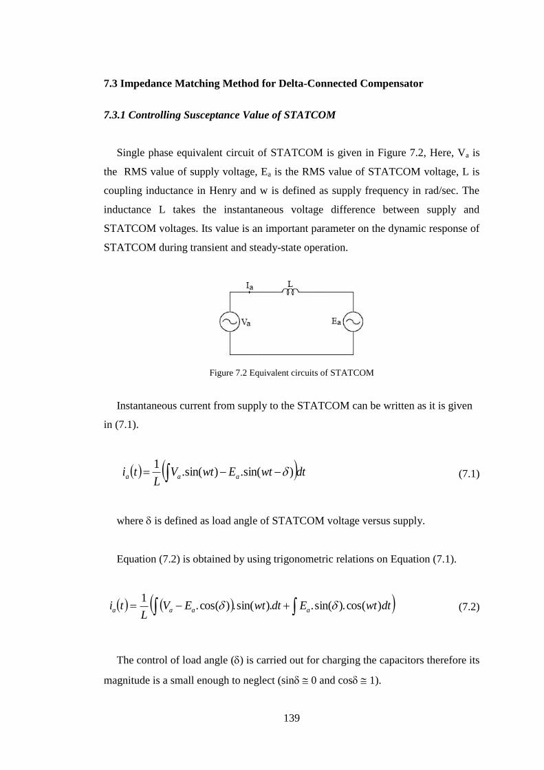
139
7.3 Impedance Matching Method for Delta-Connected Compensator
7.3.1 Controlling Susceptance Value of STATCOM
Single phase equivalent circuit of STATCOM is given in Figure 7.2, Here, Va is
the RMS value of supply voltage, Ea is the RMS value of STATCOM voltage, L is
coupling inductance in Henry and w is defined as supply frequency in rad/sec. The
inductance L takes the instantaneous voltage difference between supply and
STATCOM voltages. Its value is an important parameter on the dynamic response of
STATCOM during transient and steady-state operation.
Figure 7.2 Equivalent circuits of STATCOM
Instantaneous current from supply to the STATCOM can be written as it is given
in (7.1).
dtwtEwtVL
ti aaa )sin(.)sin(.1
(7.1)
where is defined as load angle of STATCOM voltage versus supply.
Equation (7.2) is obtained by using trigonometric relations on Equation (7.1).
dtwtEdtwtEVL
ti aaaa )cos(.)sin(..)sin(.)cos(.1
(7.2)
The control of load angle () is carried out for charging the capacitors therefore its
magnitude is a small enough to neglect (sin 0 and cos 1).
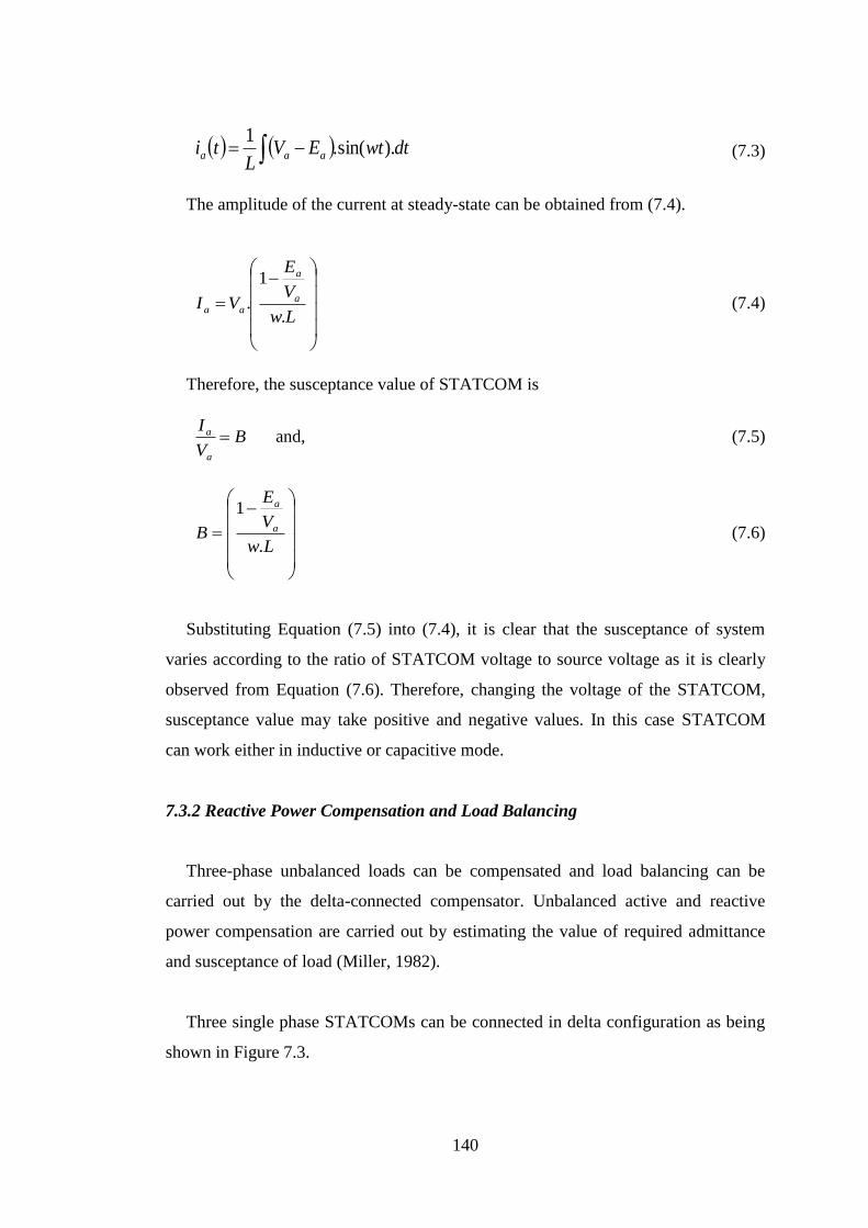
140
dtwtEVL
ti aaa ).sin(.1 (7.3)
The amplitude of the current at steady-state can be obtained from (7.4).
Lw
V
E
VI a
a
aa.
1
. (7.4)
Therefore, the susceptance value of STATCOM is
BV
I
a
a and, (7.5)
Lw
V
E
B a
a
.
1
(7.6)
Substituting Equation (7.5) into (7.4), it is clear that the susceptance of system
varies according to the ratio of STATCOM voltage to source voltage as it is clearly
observed from Equation (7.6). Therefore, changing the voltage of the STATCOM,
susceptance value may take positive and negative values. In this case STATCOM
can work either in inductive or capacitive mode.
7.3.2 Reactive Power Compensation and Load Balancing
Three-phase unbalanced loads can be compensated and load balancing can be
carried out by the delta-connected compensator. Unbalanced active and reactive
power compensation are carried out by estimating the value of required admittance
and susceptance of load (Miller, 1982).
Three single phase STATCOMs can be connected in delta configuration as being
shown in Figure 7.3.
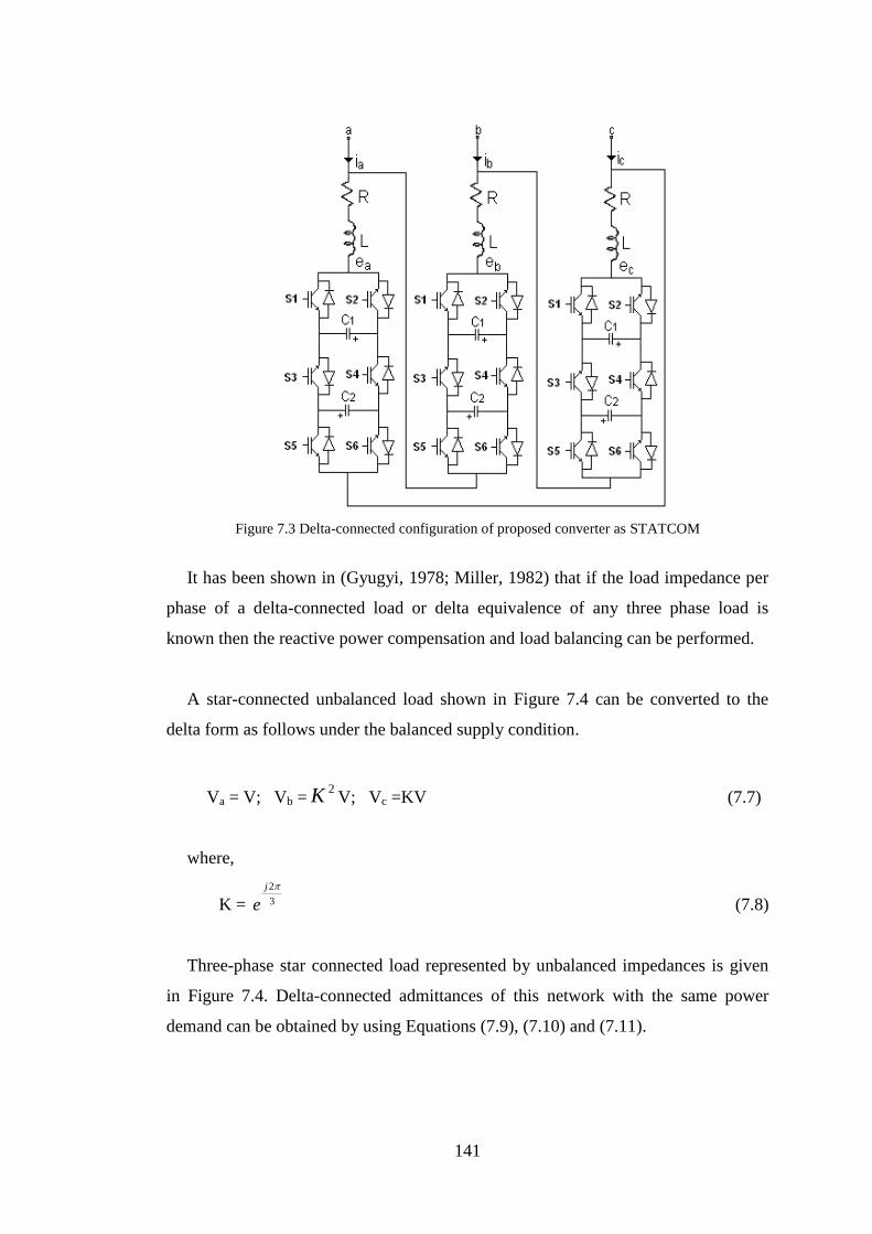
141
Figure 7.3 Delta-connected configuration of proposed converter as STATCOM
It has been shown in (Gyugyi, 1978; Miller, 1982) that if the load impedance per
phase of a delta-connected load or delta equivalence of any three phase load is
known then the reactive power compensation and load balancing can be performed.
A star-connected unbalanced load shown in Figure 7.4 can be converted to the
delta form as follows under the balanced supply condition.
Va = V; Vb =2K V; Vc =KV (7.7)
where,
K = 3
2j
e (7.8)
Three-phase star connected load represented by unbalanced impedances is given
in Figure 7.4. Delta-connected admittances of this network with the same power
demand can be obtained by using Equations (7.9), (7.10) and (7.11).

142
Figure 7.4 Three-phase wye connected load
c
accbbaab
Z
ZZZZZZZ
... (7.9)
a
accbbabc
Z
ZZZZZZZ
... (7.10)
b
accbbaca
Z
ZZZZZZZ
... (7.11)
Admittance values can be obtained from impedances as follows;
c
c
b
b
a
aY
ZY
ZY
Z1
,1
,1
(7.12)
Therefore,
cba
ba
ab
abYYY
YY
ZY
.1 (7.13)
cba
cb
bc
bcYYY
YY
ZY
.1 (7.14)
cba
ac
ca
caYYY
YY
ZY
.1 (7.15)
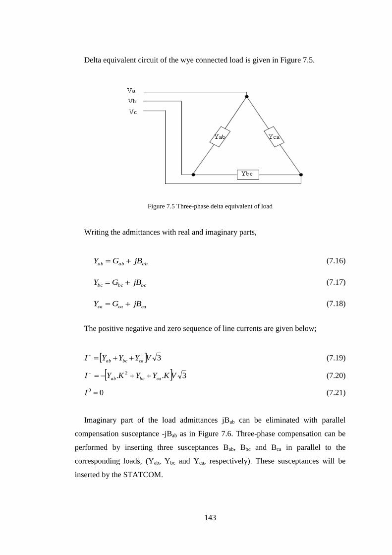
143
Delta equivalent circuit of the wye connected load is given in Figure 7.5.
Figure 7.5 Three-phase delta equivalent of load
Writing the admittances with real and imaginary parts,
ababab jBGY (7.16)
bcbcbc jBGY (7.17)
cacaca jBGY (7.18)
The positive negative and zero sequence of line currents are given below;
3VYYYI cabcab (7.19)
3.. 2 VKYYKYI cabcab (7.20)
00 I (7.21)
Imaginary part of the load admittances jBab can be eliminated with parallel
compensation susceptance -jBab as in Figure 7.6. Three-phase compensation can be
performed by inserting three susceptances Bab, Bbc and Bca in parallel to the
corresponding loads, (Yab, Ybc and Yca, respectively). These susceptances will be
inserted by the STATCOM.
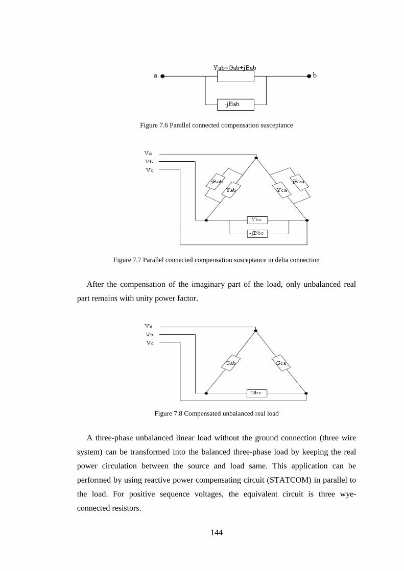
144
Figure 7.6 Parallel connected compensation susceptance
Figure 7.7 Parallel connected compensation susceptance in delta connection
After the compensation of the imaginary part of the load, only unbalanced real
part remains with unity power factor.
Figure 7.8 Compensated unbalanced real load
A three-phase unbalanced linear load without the ground connection (three wire
system) can be transformed into the balanced three-phase load by keeping the real
power circulation between the source and load same. This application can be
performed by using reactive power compensating circuit (STATCOM) in parallel to
the load. For positive sequence voltages, the equivalent circuit is three wye-
connected resistors.
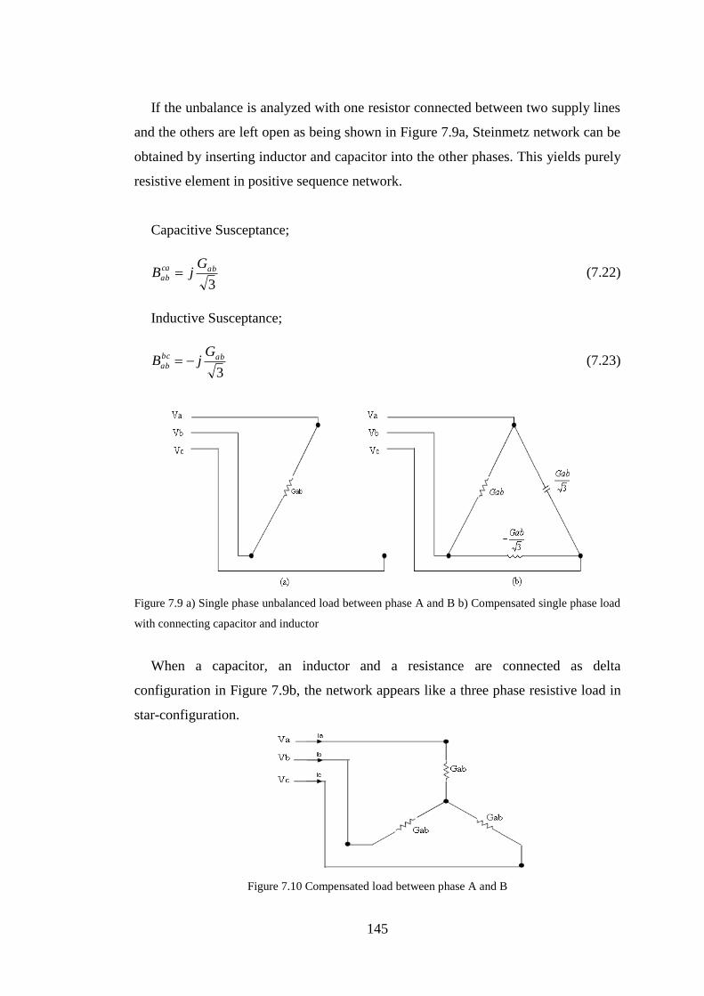
145
If the unbalance is analyzed with one resistor connected between two supply lines
and the others are left open as being shown in Figure 7.9a, Steinmetz network can be
obtained by inserting inductor and capacitor into the other phases. This yields purely
resistive element in positive sequence network.
Capacitive Susceptance;
3
abca
ab
GjB (7.22)
Inductive Susceptance;
3
abbc
ab
GjB (7.23)
Figure 7.9 a) Single phase unbalanced load between phase A and B b) Compensated single phase load
with connecting capacitor and inductor
When a capacitor, an inductor and a resistance are connected as delta
configuration in Figure 7.9b, the network appears like a three phase resistive load in
star-configuration.
Figure 7.10 Compensated load between phase A and B
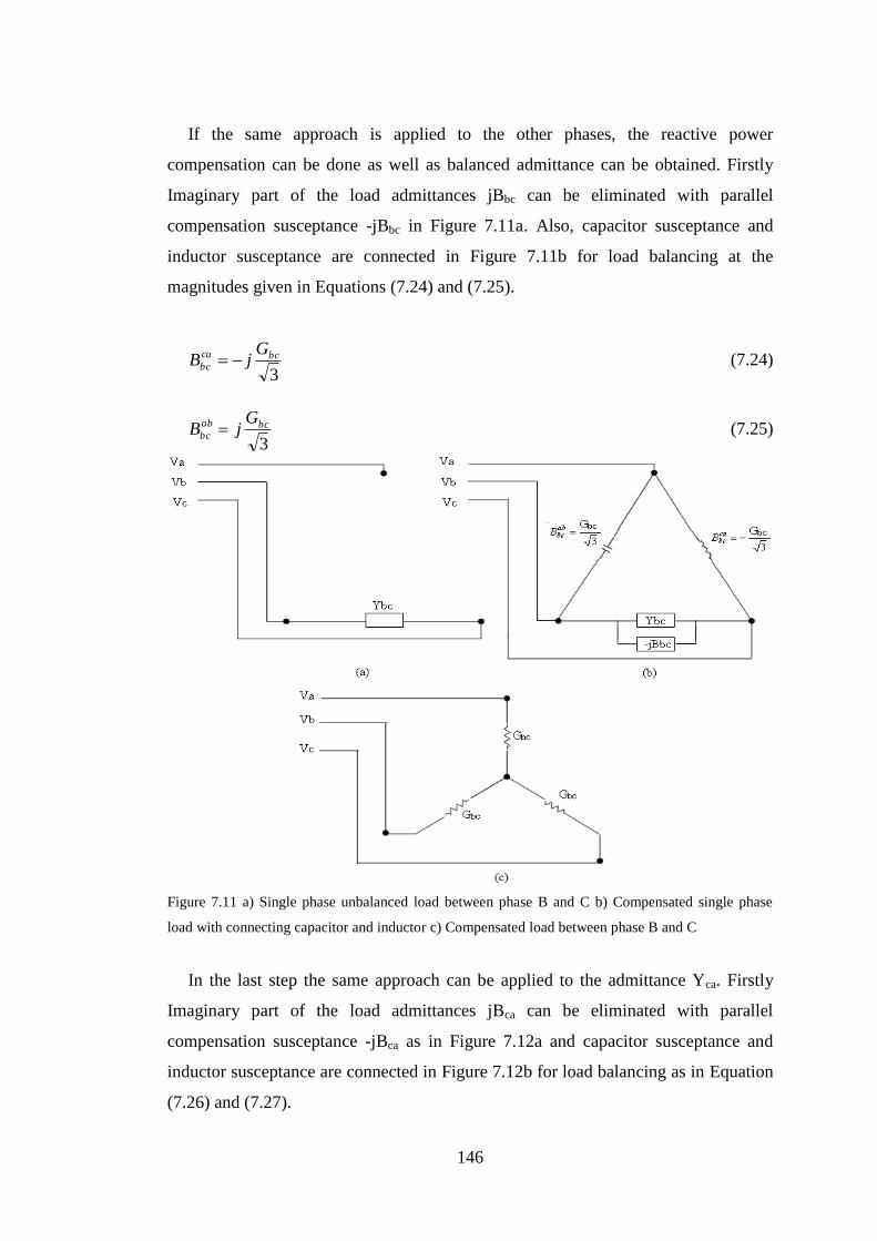
146
If the same approach is applied to the other phases, the reactive power
compensation can be done as well as balanced admittance can be obtained. Firstly
Imaginary part of the load admittances jBbc can be eliminated with parallel
compensation susceptance -jBbc in Figure 7.11a. Also, capacitor susceptance and
inductor susceptance are connected in Figure 7.11b for load balancing at the
magnitudes given in Equations (7.24) and (7.25).
3
bcca
bc
GjB (7.24)
3
bcab
bc
GjB (7.25)
Figure 7.11 a) Single phase unbalanced load between phase B and C b) Compensated single phase
load with connecting capacitor and inductor c) Compensated load between phase B and C
In the last step the same approach can be applied to the admittance Yca. Firstly
Imaginary part of the load admittances jBca can be eliminated with parallel
compensation susceptance -jBca as in Figure 7.12a and capacitor susceptance and
inductor susceptance are connected in Figure 7.12b for load balancing as in Equation
(7.26) and (7.27).

147
Figure 7.12 a) Single phase unbalanced load between phase C and A b) Compensated single phase
load with connecting capacitor and inductor c) Compensated load between phase C and A
3
caab
ca
GjB (7.26)
3
cabc
ca
GjB (7.27)
Complete compensation is obtained by adding each single balancing susceptance
from Equation (7.22) through (7.27). The resultant compensation susceptance;
Babcomp
, Bbccomp
, Bcacomp
are given in Equations (7.28), (7.29) and (7.30), respectively.
)33
( cabcab
ca
ab
bc
abab
comp
ab
GGBBBBB (7.28)
)33
( abcabc
ab
bc
ca
bcbc
comp
bc
GGBBBBB (7.29)
)33
( bcabl
ca
bc
ca
ab
caca
comp
ca
GGBBBBB (7.30)
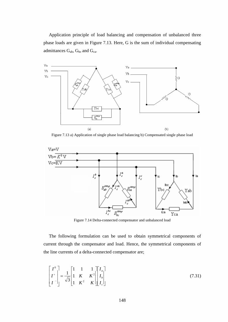
148
Application principle of load balancing and compensation of unbalanced three
phase loads are given in Figure 7.13. Here, G is the sum of individual compensating
admittances Gab, Gbc and Gca.
Figure 7.13 a) Application of single phase load balancing b) Compensated single phase load
Figure 7.14 Delta-connected compensator and unbalanced load
The following formulation can be used to obtain symmetrical components of
current through the compensator and load. Hence, the symmetrical components of
the line currents of a delta-connected compensator are;
c
b
a
I
I
I
KK
KK
I
I
I
2
2
0
1
1
111
3
1 (7.31)
149
00 compI (7.32)
3VBBBI cabcabcomp (7.33)
3.. 2 VKBBKBI cabcabcomp (7.34)
Zero, positive and negative sequence components of unbalanced load current are
obtained in Equation (7.35), (7.36) and (7.37), respectively. The value of zero
sequence components is zero because of unconnected neutral line on load. When
load is balanced, negative sequence component is cancelled out.
03
0
cba IIII (7.35)
33
2
VYYYIKKII
I cabcab
cba
(7.36)
3..3
. 2
2
VKYYKYIKIKI
I cabcab
cba
(7.37)
Eliminating imaginary part of positive sequence component of load current is
enough to compensate balanced reactive power. So, imaginary part of compensator
and load current in positive sequence should be zero. Therefore,
0Im
compII (7.38)
To compensate unbalanced reactive power of load, imaginary parts of negative
sequence component of load current and compensator should be zero. Therefore,
0Im
compII (7.39)
The real part of negative sequence component of load current and compensator
should be zero to get balanced active power transferred to the load. Therefore,
0Re
compII (7.40)
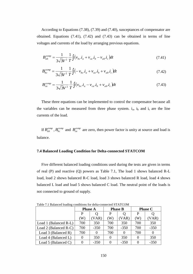
150
According to Equations (7.38), (7.39) and (7.40), susceptances of compensator are
obtained. Equations (7.41), (7.42) and (7.43) can be obtained in terms of line
voltages and currents of the load by arranging previous equations.
dtivivivTV
B cabbcaabc
comp
ab ...1
33
12
(7.41)
dtivivivTV
B cabbcaabc
comp
bc ...1
33
12
(7.42)
dtivivivTV
B cabbcaabc
comp
ca ...1
33
12
(7.43)
These three equations can be implemented to control the compensator because all
the variables can be measured from three phase system. ia, ib and ic are the line
currents of the load.
Ifcomp
abB ,comp
bcB and comp
caB are zero, then power factor is unity at source and load is
balance.
7.4 Balanced Loading Condition for Delta-connected STATCOM
Five different balanced loading conditions used during the tests are given in terms
of real (P) and reactive (Q) powers as Table 7.1, The load 1 shows balanced R-L
load, load 2 shows balanced R-C load, load 3 shows balanced R load, load 4 shows
balanced L load and load 5 shows balanced C load. The neutral point of the loads is
not connected to ground of supply.
Table 7.1 Balanced loading conditions for delta-connected STATCOM
Phase A Phase B Phase C
P
(W)
Q
(VAR)
P
(W)
Q
(VAR)
P
(W)
Q
(VAR)
Load 1 (Balanced R-L) 700 350 700 350 700 350
Load 2 (Balanced R-C) 700 -350 700 -350 700 -350
Load 3 (Balanced R) 700 0 700 0 700 0
Load 4 (Balanced L) 0 350 0 350 0 350
Load 5 (Balanced C) 0 -350 0 -350 0 -350
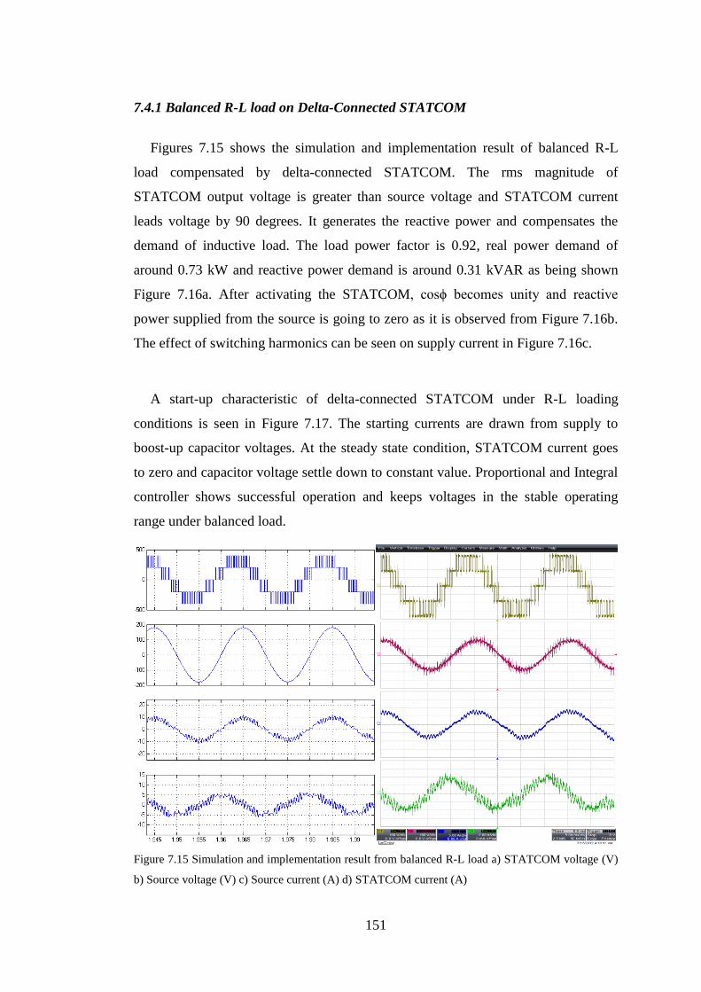
151
7.4.1 Balanced R-L load on Delta-Connected STATCOM
Figures 7.15 shows the simulation and implementation result of balanced R-L
load compensated by delta-connected STATCOM. The rms magnitude of
STATCOM output voltage is greater than source voltage and STATCOM current
leads voltage by 90 degrees. It generates the reactive power and compensates the
demand of inductive load. The load power factor is 0.92, real power demand of
around 0.73 kW and reactive power demand is around 0.31 kVAR as being shown
Figure 7.16a. After activating the STATCOM, cosϕ becomes unity and reactive
power supplied from the source is going to zero as it is observed from Figure 7.16b.
The effect of switching harmonics can be seen on supply current in Figure 7.16c.
A start-up characteristic of delta-connected STATCOM under R-L loading
conditions is seen in Figure 7.17. The starting currents are drawn from supply to
boost-up capacitor voltages. At the steady state condition, STATCOM current goes
to zero and capacitor voltage settle down to constant value. Proportional and Integral
controller shows successful operation and keeps voltages in the stable operating
range under balanced load.
Figure 7.15 Simulation and implementation result from balanced R-L load a) STATCOM voltage (V)
b) Source voltage (V) c) Source current (A) d) STATCOM current (A)
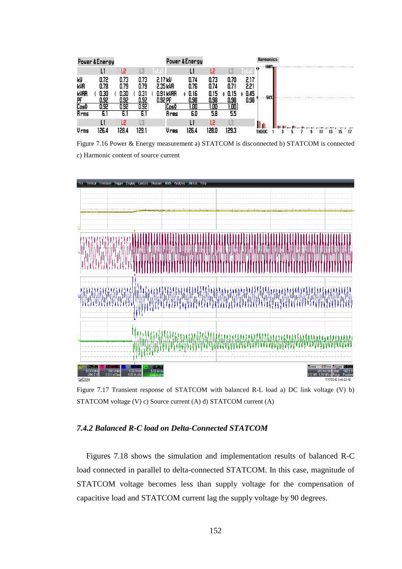
152
Figure 7.16 Power & Energy measurement a) STATCOM is disconnected b) STATCOM is connected
c) Harmonic content of source current
Figure 7.17 Transient response of STATCOM with balanced R-L load a) DC link voltage (V) b)
STATCOM voltage (V) c) Source current (A) d) STATCOM current (A)
7.4.2 Balanced R-C load on Delta-Connected STATCOM
Figures 7.18 shows the simulation and implementation results of balanced R-C
load connected in parallel to delta-connected STATCOM. In this case, magnitude of
STATCOM voltage becomes less than supply voltage for the compensation of
capacitive load and STATCOM current lag the supply voltage by 90 degrees.
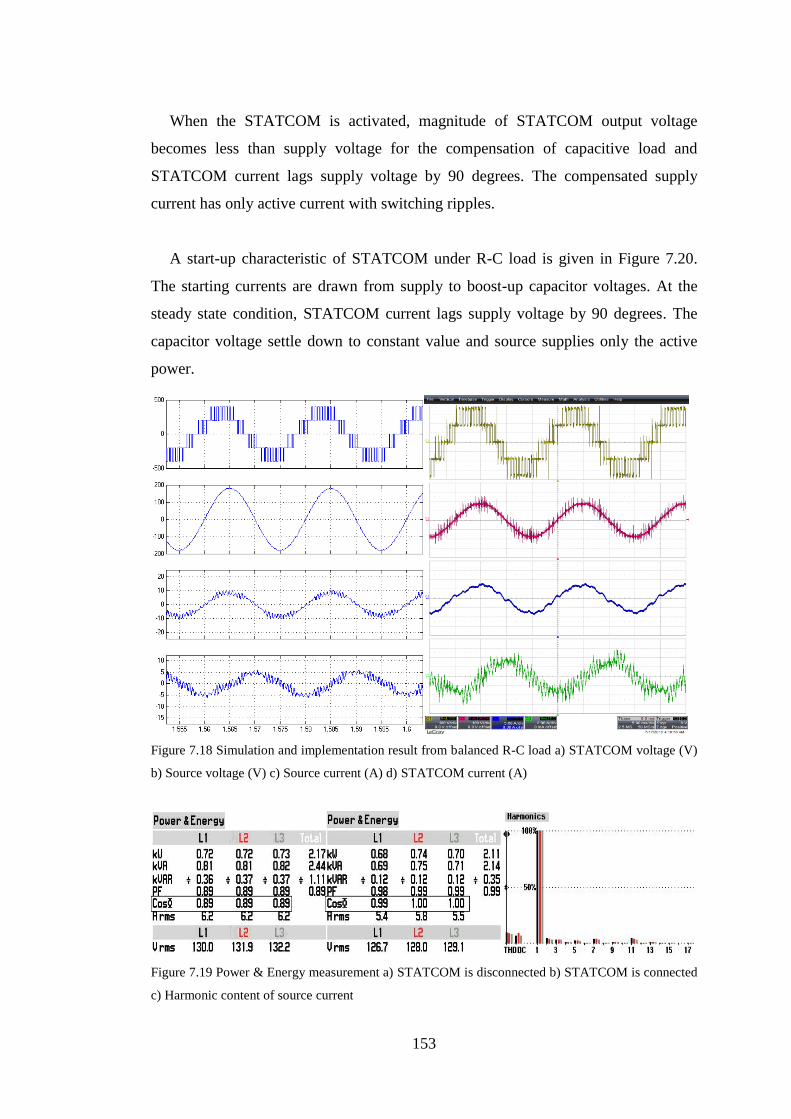
153
When the STATCOM is activated, magnitude of STATCOM output voltage
becomes less than supply voltage for the compensation of capacitive load and
STATCOM current lags supply voltage by 90 degrees. The compensated supply
current has only active current with switching ripples.
A start-up characteristic of STATCOM under R-C load is given in Figure 7.20.
The starting currents are drawn from supply to boost-up capacitor voltages. At the
steady state condition, STATCOM current lags supply voltage by 90 degrees. The
capacitor voltage settle down to constant value and source supplies only the active
power.
Figure 7.18 Simulation and implementation result from balanced R-C load a) STATCOM voltage (V)
b) Source voltage (V) c) Source current (A) d) STATCOM current (A)
Figure 7.19 Power & Energy measurement a) STATCOM is disconnected b) STATCOM is connected
c) Harmonic content of source current

154
Figure 7.20 Transient response of STATCOM with balanced R-C load a) DC link voltage (V) b)
STATCOM voltage (V) c) Source current (A) d) STATCOM current (A)
7.4.3 Balanced R load on Delta-Connected STATCOM
Figure 7.21 shows the simulation and implementation results of balanced R load
and its parameters are given in Table 6.2. Each phase only have resistive balanced
load. So STATCOM should not absorb or generate any reactive power under
resistive load.
In Figure 7.22a, each phase draws 0.7 KW real power and 0.01 KVAR reactive
powers. After activating the STATCOM, cosϕ becomes unity as it is shown in Figure
7.22b. The rms magnitude of STATCOM output voltage is equal to supply voltage
and STATCOM draws small amount active power to be keep voltage level of
capacitor at predefined value. Switching ripples on STATCOM current also affects
the supply current as it is observed from Figure 7.21c.
Start-up characteristics of STATCOM are given in Figure 7.23. The starting
currents are drawn from supply to boost-up capacitor voltages. At the steady state
condition, STATCOM current goes to zero, capacitor voltage settle down to constant
value and supply current and supply voltage come back to in phase.

155
Figure 7.21 Simulation and implementation result from Balanced R load a) STATCOM voltage (V) b)
Source voltage (V) c) Source current (A) d) STATCOM current (A)
Figure 7.22 Power & Energy measurement a) STATCOM is disconnected b) STATCOM is connected
c) Harmonic content of source current
Figure 7.23 Transient response of STATCOM with balanced R load a) DC link voltage (V) b)
STATCOM voltage (V) c) Source current (A) d) STATCOM current (A)

156
7.4.4 Balanced L load on Delta-Connected STATCOM
Compensation of balanced inductive loading condition is confirmed by simulation
and implementation in Figures 7.24. Magnitude of STATCOM output voltage should
be greater than supply voltage and STATCOM current must lead supply voltage by
90 degrees to compensate the pure inductive load. In supply current, the effect of
switching ripples is observed in Figure 7.24c.
Before STATCOM is activated, energy analyzer measures power factor (cosϕ) as
zero Figure 7.25a. When STATCOM is activated cosϕ becomes unity. But power
quality analyzer is reading reactive power incorrectly because the only switching
ripples are available on supply current.
Start-up characteristics of STATCOM are given in Figure 7.26. The starting
currents are drawn from supply to boost-up capacitor voltages. At the steady state
condition, STATCOM current leads supply voltage by 90 degrees. The capacitor
voltage settle down to constant value and source current goes to zero.
Figure 7.24 Simulation and implementation result from balanced L load a) STATCOM voltage (V) b)
Source voltage (V) c) Source current (A) d) STATCOM current (A)
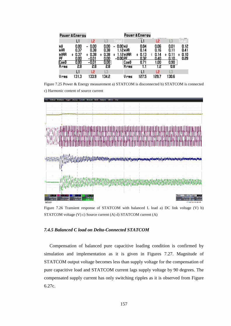
157
Figure 7.25 Power & Energy measurement a) STATCOM is disconnected b) STATCOM is connected
c) Harmonic content of source current
Figure 7.26 Transient response of STATCOM with balanced L load a) DC link voltage (V) b)
STATCOM voltage (V) c) Source current (A) d) STATCOM current (A)
7.4.5 Balanced C load on Delta-Connected STATCOM
Compensation of balanced pure capacitive loading condition is confirmed by
simulation and implementation as it is given in Figures 7.27. Magnitude of
STATCOM output voltage becomes less than supply voltage for the compensation of
pure capacitive load and STATCOM current lags supply voltage by 90 degrees. The
compensated supply current has only switching ripples as it is observed from Figure
6.27c.
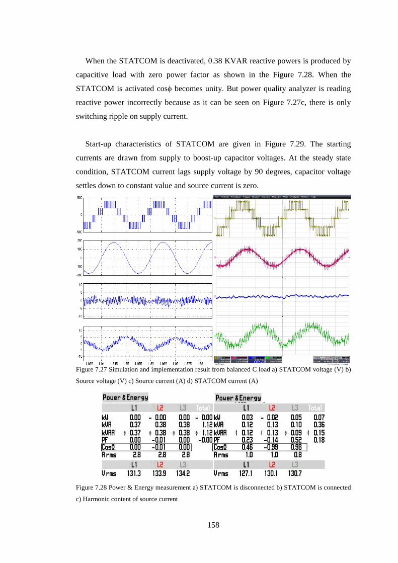
158
When the STATCOM is deactivated, 0.38 KVAR reactive powers is produced by
capacitive load with zero power factor as shown in the Figure 7.28. When the
STATCOM is activated cosϕ becomes unity. But power quality analyzer is reading
reactive power incorrectly because as it can be seen on Figure 7.27c, there is only
switching ripple on supply current.
Start-up characteristics of STATCOM are given in Figure 7.29. The starting
currents are drawn from supply to boost-up capacitor voltages. At the steady state
condition, STATCOM current lags supply voltage by 90 degrees, capacitor voltage
settles down to constant value and source current is zero.
Figure 7.27 Simulation and implementation result from balanced C load a) STATCOM voltage (V) b)
Source voltage (V) c) Source current (A) d) STATCOM current (A)
Figure 7.28 Power & Energy measurement a) STATCOM is disconnected b) STATCOM is connected
c) Harmonic content of source current
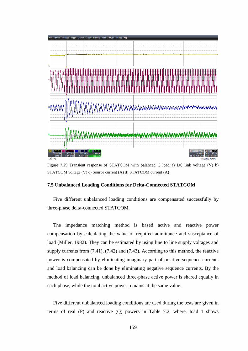
159
Figure 7.29 Transient response of STATCOM with balanced C load a) DC link voltage (V) b)
STATCOM voltage (V) c) Source current (A) d) STATCOM current (A)
7.5 Unbalanced Loading Conditions for Delta-Connected STATCOM
Five different unbalanced loading conditions are compensated successfully by
three-phase delta-connected STATCOM.
The impedance matching method is based active and reactive power
compensation by calculating the value of required admittance and susceptance of
load (Miller, 1982). They can be estimated by using line to line supply voltages and
supply currents from (7.41), (7.42) and (7.43). According to this method, the reactive
power is compensated by eliminating imaginary part of positive sequence currents
and load balancing can be done by eliminating negative sequence currents. By the
method of load balancing, unbalanced three-phase active power is shared equally in
each phase, while the total active power remains at the same value.
Five different unbalanced loading conditions are used during the tests are given in
terms of real (P) and reactive (Q) powers in Table 7.2, where, load 1 shows
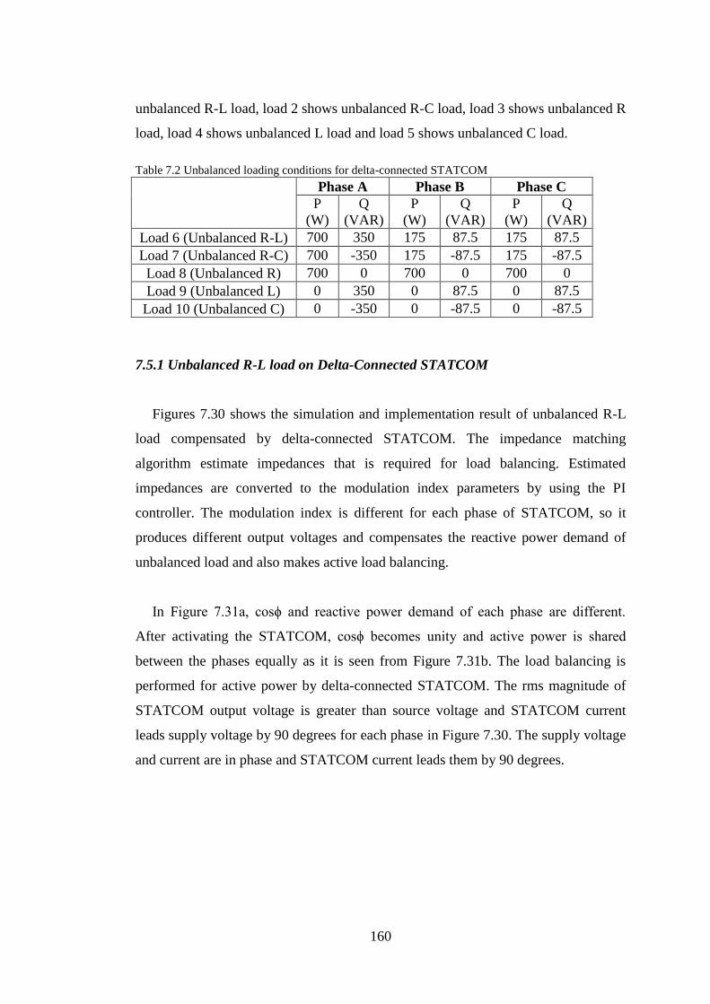
160
unbalanced R-L load, load 2 shows unbalanced R-C load, load 3 shows unbalanced R
load, load 4 shows unbalanced L load and load 5 shows unbalanced C load.
Table 7.2 Unbalanced loading conditions for delta-connected STATCOM
Phase A Phase B Phase C
P
(W)
Q
(VAR)
P
(W)
Q
(VAR)
P
(W)
Q
(VAR)
Load 6 (Unbalanced R-L) 700 350 175 87.5 175 87.5
Load 7 (Unbalanced R-C) 700 -350 175 -87.5 175 -87.5
Load 8 (Unbalanced R) 700 0 700 0 700 0
Load 9 (Unbalanced L) 0 350 0 87.5 0 87.5
Load 10 (Unbalanced C) 0 -350 0 -87.5 0 -87.5
7.5.1 Unbalanced R-L load on Delta-Connected STATCOM
Figures 7.30 shows the simulation and implementation result of unbalanced R-L
load compensated by delta-connected STATCOM. The impedance matching
algorithm estimate impedances that is required for load balancing. Estimated
impedances are converted to the modulation index parameters by using the PI
controller. The modulation index is different for each phase of STATCOM, so it
produces different output voltages and compensates the reactive power demand of
unbalanced load and also makes active load balancing.
In Figure 7.31a, cosϕ and reactive power demand of each phase are different.
After activating the STATCOM, cosϕ becomes unity and active power is shared
between the phases equally as it is seen from Figure 7.31b. The load balancing is
performed for active power by delta-connected STATCOM. The rms magnitude of
STATCOM output voltage is greater than source voltage and STATCOM current
leads supply voltage by 90 degrees for each phase in Figure 7.30. The supply voltage
and current are in phase and STATCOM current leads them by 90 degrees.
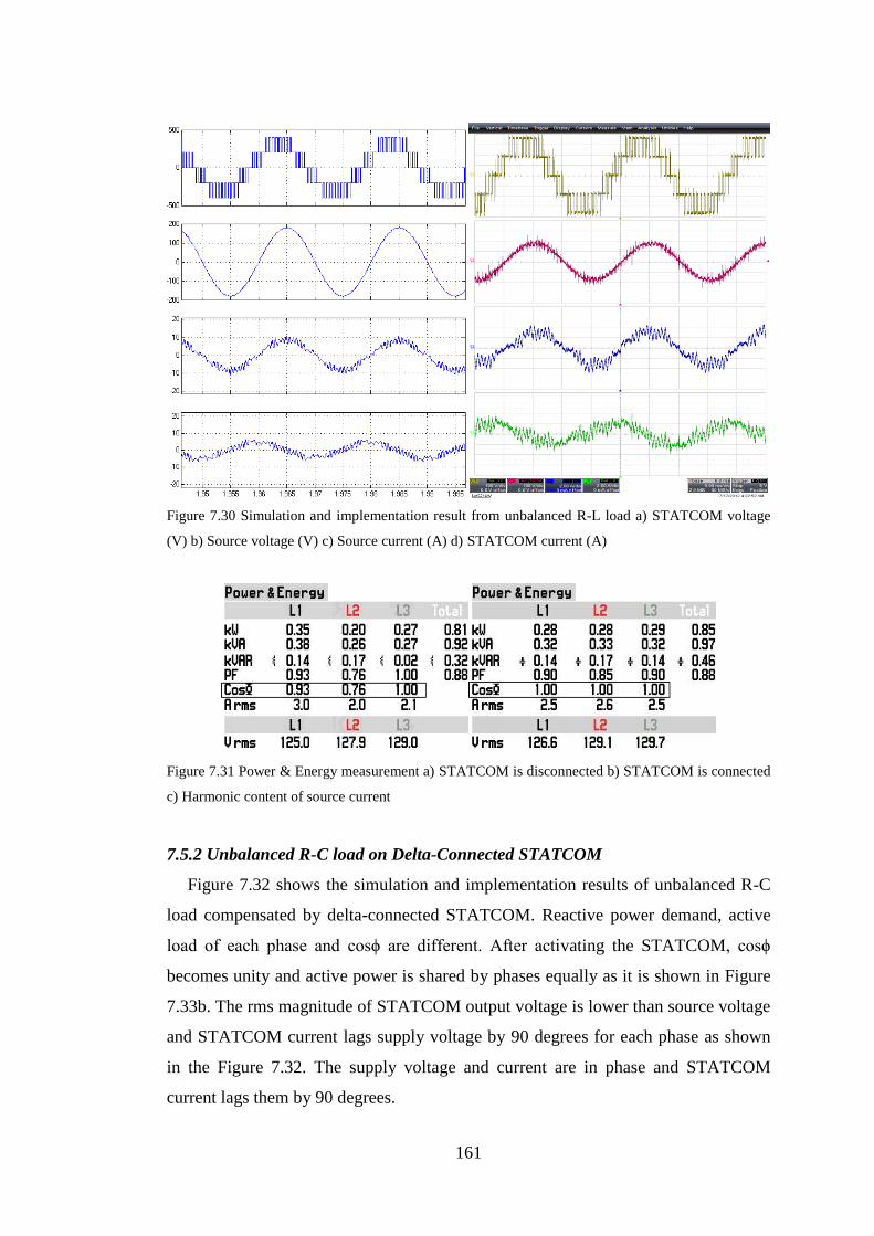
161
Figure 7.30 Simulation and implementation result from unbalanced R-L load a) STATCOM voltage
(V) b) Source voltage (V) c) Source current (A) d) STATCOM current (A)
Figure 7.31 Power & Energy measurement a) STATCOM is disconnected b) STATCOM is connected
c) Harmonic content of source current
7.5.2 Unbalanced R-C load on Delta-Connected STATCOM
Figure 7.32 shows the simulation and implementation results of unbalanced R-C
load compensated by delta-connected STATCOM. Reactive power demand, active
load of each phase and cosϕ are different. After activating the STATCOM, cosϕ
becomes unity and active power is shared by phases equally as it is shown in Figure
7.33b. The rms magnitude of STATCOM output voltage is lower than source voltage
and STATCOM current lags supply voltage by 90 degrees for each phase as shown
in the Figure 7.32. The supply voltage and current are in phase and STATCOM
current lags them by 90 degrees.
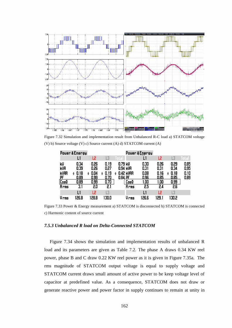
162
Figure 7.32 Simulation and implementation result from Unbalanced R-C load a) STATCOM voltage
(V) b) Source voltage (V) c) Source current (A) d) STATCOM current (A)
Figure 7.33 Power & Energy measurement a) STATCOM is disconnected b) STATCOM is connected
c) Harmonic content of source current
7.5.3 Unbalanced R load on Delta-Connected STATCOM
Figure 7.34 shows the simulation and implementation results of unbalanced R
load and its parameters are given as Table 7.2. The phase A draws 0.34 KW reel
power, phase B and C draw 0.22 KW reel power as it is given in Figure 7.35a. The
rms magnitude of STATCOM output voltage is equal to supply voltage and
STATCOM current draws small amount of active power to be keep voltage level of
capacitor at predefined value. As a consequence, STATCOM does not draw or
generate reactive power and power factor in supply continues to remain at unity in
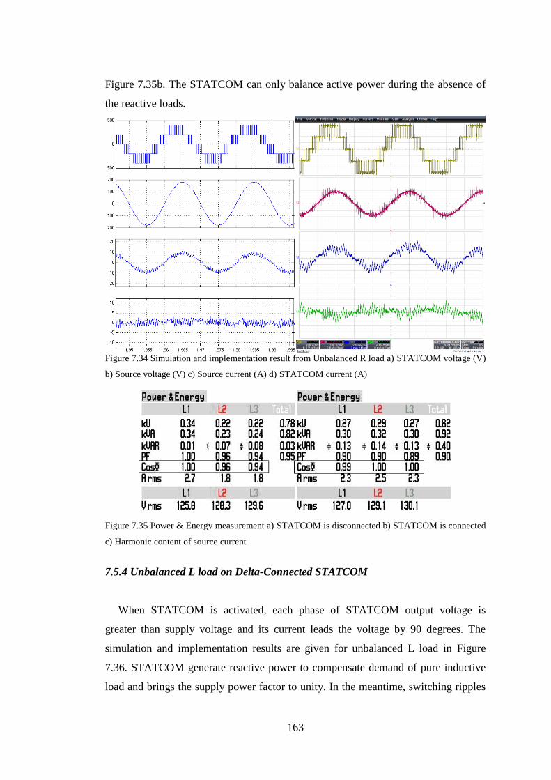
163
Figure 7.35b. The STATCOM can only balance active power during the absence of
the reactive loads.
Figure 7.34 Simulation and implementation result from Unbalanced R load a) STATCOM voltage (V)
b) Source voltage (V) c) Source current (A) d) STATCOM current (A)
Figure 7.35 Power & Energy measurement a) STATCOM is disconnected b) STATCOM is connected
c) Harmonic content of source current
7.5.4 Unbalanced L load on Delta-Connected STATCOM
When STATCOM is activated, each phase of STATCOM output voltage is
greater than supply voltage and its current leads the voltage by 90 degrees. The
simulation and implementation results are given for unbalanced L load in Figure
7.36. STATCOM generate reactive power to compensate demand of pure inductive
load and brings the supply power factor to unity. In the meantime, switching ripples
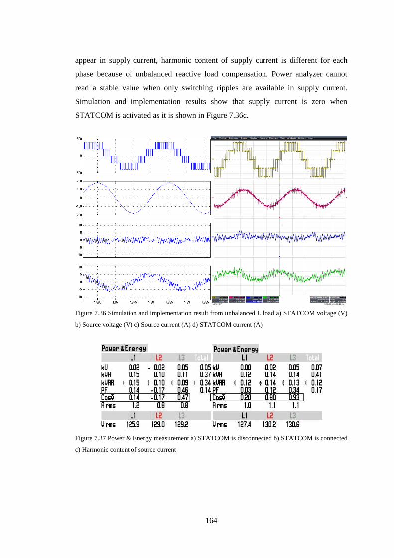
164
appear in supply current, harmonic content of supply current is different for each
phase because of unbalanced reactive load compensation. Power analyzer cannot
read a stable value when only switching ripples are available in supply current.
Simulation and implementation results show that supply current is zero when
STATCOM is activated as it is shown in Figure 7.36c.
Figure 7.36 Simulation and implementation result from unbalanced L load a) STATCOM voltage (V)
b) Source voltage (V) c) Source current (A) d) STATCOM current (A)
Figure 7.37 Power & Energy measurement a) STATCOM is disconnected b) STATCOM is connected
c) Harmonic content of source current
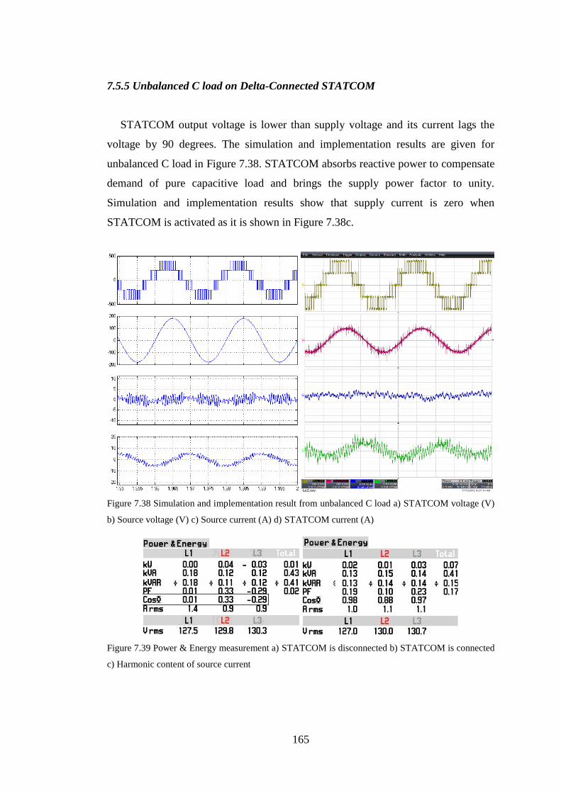
165
7.5.5 Unbalanced C load on Delta-Connected STATCOM
STATCOM output voltage is lower than supply voltage and its current lags the
voltage by 90 degrees. The simulation and implementation results are given for
unbalanced C load in Figure 7.38. STATCOM absorbs reactive power to compensate
demand of pure capacitive load and brings the supply power factor to unity.
Simulation and implementation results show that supply current is zero when
STATCOM is activated as it is shown in Figure 7.38c.
Figure 7.38 Simulation and implementation result from unbalanced C load a) STATCOM voltage (V)
b) Source voltage (V) c) Source current (A) d) STATCOM current (A)
Figure 7.39 Power & Energy measurement a) STATCOM is disconnected b) STATCOM is connected
c) Harmonic content of source current
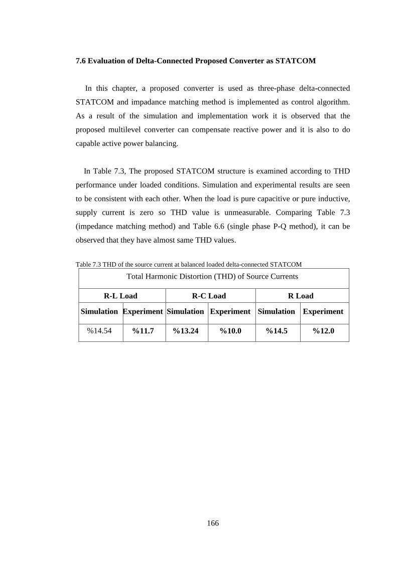
166
7.6 Evaluation of Delta-Connected Proposed Converter as STATCOM
In this chapter, a proposed converter is used as three-phase delta-connected
STATCOM and impadance matching method is implemented as control algorithm.
As a result of the simulation and implementation work it is observed that the
proposed multilevel converter can compensate reactive power and it is also to do
capable active power balancing.
In Table 7.3, The proposed STATCOM structure is examined according to THD
performance under loaded conditions. Simulation and experimental results are seen
to be consistent with each other. When the load is pure capacitive or pure inductive,
supply current is zero so THD value is unmeasurable. Comparing Table 7.3
(impedance matching method) and Table 6.6 (single phase P-Q method), it can be
observed that they have almost same THD values.
Table 7.3 THD of the source current at balanced loaded delta-connected STATCOM
Total Harmonic Distortion (THD) of Source Currents
R-L Load R-C Load R Load
Simulation Experiment Simulation Experiment Simulation Experiment
%14.54 %11.7 %13.24 %10.0 %14.5 %12.0
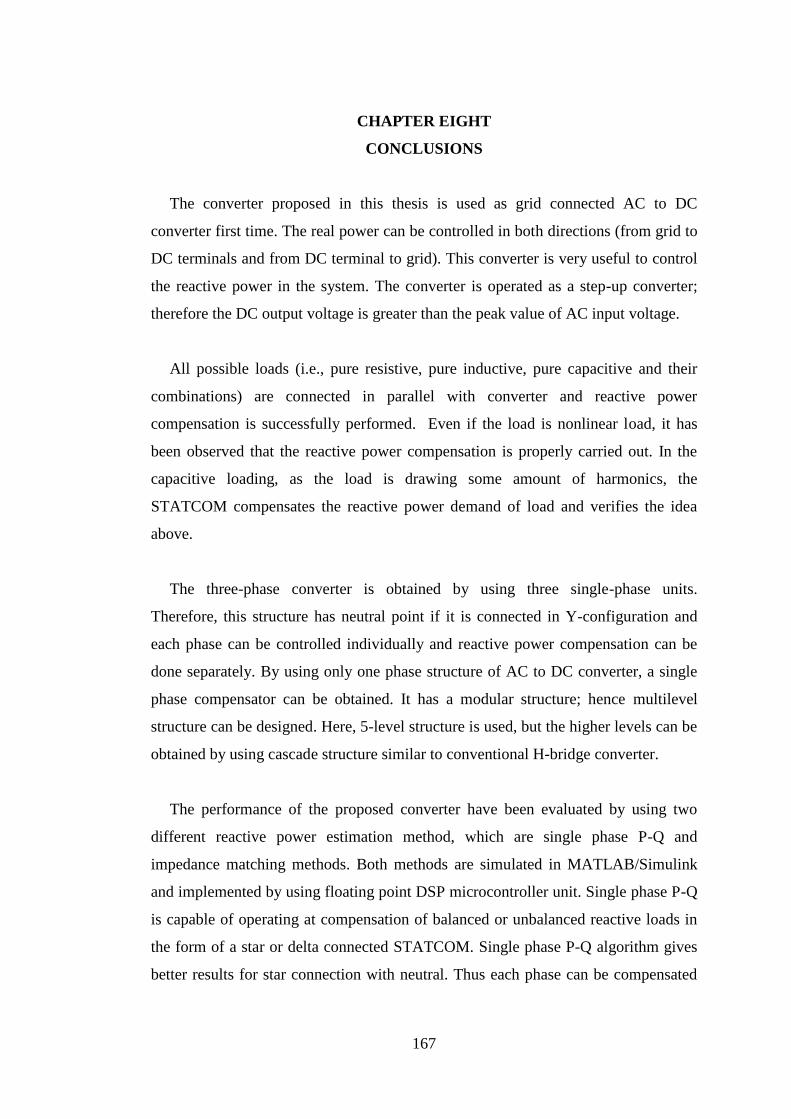
167
CHAPTER EIGHT
CONCLUSIONS
The converter proposed in this thesis is used as grid connected AC to DC
converter first time. The real power can be controlled in both directions (from grid to
DC terminals and from DC terminal to grid). This converter is very useful to control
the reactive power in the system. The converter is operated as a step-up converter;
therefore the DC output voltage is greater than the peak value of AC input voltage.
All possible loads (i.e., pure resistive, pure inductive, pure capacitive and their
combinations) are connected in parallel with converter and reactive power
compensation is successfully performed. Even if the load is nonlinear load, it has
been observed that the reactive power compensation is properly carried out. In the
capacitive loading, as the load is drawing some amount of harmonics, the
STATCOM compensates the reactive power demand of load and verifies the idea
above.
The three-phase converter is obtained by using three single-phase units.
Therefore, this structure has neutral point if it is connected in Y-configuration and
each phase can be controlled individually and reactive power compensation can be
done separately. By using only one phase structure of AC to DC converter, a single
phase compensator can be obtained. It has a modular structure; hence multilevel
structure can be designed. Here, 5-level structure is used, but the higher levels can be
obtained by using cascade structure similar to conventional H-bridge converter.
The performance of the proposed converter have been evaluated by using two
different reactive power estimation method, which are single phase P-Q and
impedance matching methods. Both methods are simulated in MATLAB/Simulink
and implemented by using floating point DSP microcontroller unit. Single phase P-Q
is capable of operating at compensation of balanced or unbalanced reactive loads in
the form of a star or delta connected STATCOM. Single phase P-Q algorithm gives
better results for star connection with neutral. Thus each phase can be compensated
168
independently. Simulation and implementation results show that single phase P-Q
and proposed converter can be used for non-linear loads under one phase, balanced
three-phase and unbalanced loading conditions if the star connection is performed
with neutral line. The impedance matching method that can only works for delta
connection of STATCOM. Delta connected proposed converter with impedance
matching method can compensate balanced or unbalanced reactive loads and share
active power among three phase equally according to simulation and implementation
results.
A detailed average value model of the proposed multilevel STATCOM has been
obtained at the synchronously rotating reference frame for single phase converter.
Average value model of switching function that is level shifted carrier based SPWM,
is also obtained by taking care the defined time intervals. Simulation results of
Matlab/Simulink and single phase d-q model are compared with each other for
transient and steady-state operations.
A novel converter for a three-phase STATCOM with reduced number of switches
is modelled, simulated and tested. All results from the dedicated model, Simulink
and implementation work are compared with each other and it is verified that this
converter has all the features of conventional H-bridge converter.
FURTHER WORK:
Since this converter is designed and implemented first time due to best of our
knowledge depending on published literature, there are several works to be done on
it. Most important ones are as follows:
i) The power loss on the converter should be analyzed based on applied
mathematics and experimental work. A detailed comparison should be
made with the conventional structures, such as H-bridge structure.
ii) This converter can be used in the application of active power filters,
therefore a detailed study should be carried out in that field.

169
iii) This converter can be used in high voltage direct current (HVDC)
application; therefore, possible problems with the application should be
investigated.
iv) In multilevel application, the problems with levels more than five should
be investigated on this converter structure.
170
REFERENCES
Abu-Rub, H., Holtz, J., Rodriquez, J., & Boaming, G. (2010). Medium-voltage
multilevel converters-state of the art, challenges, and requirements in industrial
applications, IEEE Transactions on Industrial Electronics, 57, (8), 2581-2596.
Akagi, H., Kazanawa, Y., & Nabae, A., (1984). Instantaneous reactive power
compensators comprising switching devices without energy storage components.
IEEE Transaction on Industry Applications, 20, (3), 625-630.
Al-Hadidi, H.K., & Menzies, R.W., (2003). Investigation of a cascade multilevel
inverter as an STATCOM, Power Engineering Society General Meeting IEEE, 1,
187-193.
Arrillaga, J., & Watson, N.R. (2003). Power System Harmonics, John Wiley & Sons
Babaei, E. (2008). A cascade multilevel converter topology with reduced number of
switches, IEEE Transaction on Power Electronics, 23, (6), 2657-2664.
Balikci, A., & Akpinar, E. (2010). Analysis of STATCOM under 3 phase balanced
reactive load, Electrical, Electronics and Computer Engineering National
Conference on, 137–141.
Balikci, A., & Akpinar, E. (2011). A novel multilevel converter used for three phase
STATCOM under unbalanced load. Electrical Machines and Power Electronics
and Electromotion Joint Conference, 158–163.
Balikci, A., & Akpinar, E. (2012a). A three-phase four wire STATCOM with
reduced number of switches for unbalanced loads, The 10th International
Conference on AC and DC Power Transmission IET, 1-6.
Balikci, A., Akpinar, E.,,Vardar, K. & Azizoglu, B. (2012b). Design and PSPICE
analysis of a grid connected multilevel converter with reduced number of
switches. AC and DC Power Transmission, 1–6.
171
Balikci, A., & Akpinar, E. (2013). A three-phase four wire static synchronous
compensator with reduced number of switches for unbalanced loads, IET Power
Electronics.
Banaei, M.R., & Salary, E. (2011). Analysis of a generalized symmetrical
multilevel inverter. Journal of Circuits, Systems, and Computers, 20, (299),
299-311.
Bhavaraju, V.B., & Enjeti P.N., (1993). Analysis and design of an active power filter
for balancing unbalanced loads, IEEE Transaction on Power Electronics, 8, (4),
640-647
Blasko, V., & Kaura, V. (1997). A new mathematical model and control of a three-
phase AC-DC voltage source converter, IEEE Transaction on Power Electronics,
12, (1), 116-123.
Chattopadhyay, S., Mitra, M., & Senqupta, S. (2011). Electric Power Quality.
Springer
Chen, Y., Mwinyiwiwa, B., Wolanski, Z., & Ooi, B.T. (1997). Regulating and
equalizing DC capacitance voltages in multilevel STATCOM, IEEE Transaction
on Industrial Application, 12, (2), 901-907.
Cheng, Y., Qian, C., Crow, M.L., Pekarek, S., & Atcitty, S. (2006). A comparison of
diode-clamped and cascaded multilevel converters for a STATCOM with energy
storage, IEEE Transaction on Industial Electronics, 53, (5), 1512-1521.
Chung, S.K. (2000). Phase-locked loop for grid-connected three-phase power
conversion systems, IEE Proceedings Electric Power Applications, 147, (3), 213-
219.
Gultekin, B., Gerçek, C.O., Atalik, T., Deniz, M., Biçer, N., Ermis, M., et al.
(2012). Design and implementation of a 154 KV ±50-MVAR transmission
STATCOM based on 21-Level cascaded multilevel converter. IEEE transaction
on Industry Applications, 48, 3, 1030–1045.

172
Gültekin, B., & Ermis, M. (2013). Cascaded multilevel converter-based transmission
STATCOM: system design methodology and development of a 12 kv ±12Mvar
power stage, IEEE Transaction on Power Electronic, 28, (11), 4930-4950.
Gyugyi, L., Otto, R.A., & Putman T.H. (1978). Prınciples and applications of static,
thyristor-controlled shunt compensators, IEEE Transaction on Power Apparatus
and Systems, 97, (5), 1935-1945.
Hagiwara, M., Akagi, H. (2009). Control and experiment of pulsewidth-modulated
modular multilevel converters, IEEE Transaction on Power Electronics, 24, (7),
1737 – 1746.
Haque, M.T.(2002). Single-phase PQ theory. 33rd Annual IEEE Power Electronic
Specialist Conference, 4, 1815-1820.
Hingorani, N.G.,& Gyugyul, L. (1999), Understanding FACTS, IEEE Press
IEEE Std 1459-2010 (2010). IEEE standard definition for the measurement of
electric power quantities under sinusoidal, nonsinusoidal, balanced, or
unbalanced conditions
IEEE Terms and Definitions, (1997). Proposed terms and definition for flexible AC
transmission system, IEEE Transaction on Power Delivery, 12, (4), 1848-1853
Jiangchao, Q., & Saeedifard, M. (2012). Predictive control of a modular multilevel
converter for a back to back hvdc system, IEEE Transaction on Power Delivery,
27, (3), 1538-1547.
Khadkikar, V., Chandra, A., & Singh, B.N. (2009). Generalised single-phase P-Q
theory for active power filtering: simulation and DSP-based experimental
investigation. IET Power Electronics, 2, (1), 67-78.
Kumar, A.K., & Padiyar, K.R. (2008). Modeling, analysis and control of a chain cell
converter, Power System Technology and IEEE Power India Conference, 1-8.
173
Kumar, J., Das, B., & Agarwal, P. (2009). Modeling of 11-Level cascade multilevel
STATCOM, International Journal of Recent Trends in Engineering, 2, (5), 352-
356.
Lai, J.S., & Peng F.Z. (1996). Multilevel converters-A new breed of power
converters, IEEE Transaction on Industry Applications, 32, (3), 509-517.
Lesnicar, A., & Marquardt, R. (2003). An innovative modular multilevel converter
topology suitable for a wide power range, Power Tech Conference IEEE
Bologna, 3.
Lim, T.C., Williams, B.W. & Finney, S.J. (2010). Active snubber energy recovery
circuit for series-connected IGBTs, IEEE Transaction on Power Electronics, 26,
(7), 1879-1889.
Malinowski, M., Gopakumar, K., Rodriguez, J., & Pérez, M.A. (2010). A survey on
cascaded multilevel inverters, IEEE Transaction on Industrial Electronics, 57,
(7), 2197-2206.
McGrath, B.P., & Holmes, D.G. (2002). Multicarrier PWM strategies for multilevel
inverters, IEEE Transaction on Industrial Electronics, 49, (4), 858-867.
Miller, T.H.E.(1982) Reactive Power Control in Electrical Systems, John Willey &
Sons
Mishra, M.K., Karthikeyan, K., & Linash, P.K. (2006). A development and
implementation of DSP based DSTATCOM to compensate unbalanced
nonlinear loads, Power India Conference.
Mulla, M.A., Rajagopalan, C., & Chowdhury, A. (2013). Hardware
implementation of series hybrid active power filter using a novel control
strategy based on generalised instantaneous power theory, IET Power
Electronics, 6, (3), 592-600.
Nabae, A., Takahashi, I., & Akagi, H. (1981). A new neutral-point-clamped PWM
inverter, IEEE transactions on Industry Applications, 1, (17), 518-523.
174
Peng, F.Z., Lai, J.S., McKeever, J., & Coevering, J.V. (1996). A multilevel voltage-
source inverter with separate DC sources for static VAR generation, IEEE
Transaction on Industry Application, 32, (5), 1130-1138.
Peng, F.Z., Mckeever, J.W., & Adams DJ. (1997). Cascade multilevel inverters for
utility applications, Industrial Electronics, Control and Instrumentation, 2, 437-
442.
Peng, F.Z., Lai, J.S., McKeever, J., & Coevering, J.V. (1998). A power line
conditioner using cascade multilevel inverter for distribution system, IEEE
Transaction on Industry Applications, 34, (6), 1293-1298.
Peng, F.Z., & Wang, J. (2004). A Universal STATCOM with delta-connected
cascade multilevel inverter, Power Electronics Specialists Conference, 5, 3529-
3533.
Phipps, W., Harrison, M.J., & Duke, R.M. (2006). Three-phase phase-locked loop
control of a new generation power converter, 1ST IEEE Conference on Industrial
Electronics and Applications.
Rao, P., Crow, M.L., & Yang, Z. (2000). STATCOM control for power system
voltage control applications, IEEE Transaction on Power Delivery, 15, (4), 1311-
1317.
Rashid, M. H., (2006), Power electronics handbook, New York: Academic Press
Rodriguez, J., Lai, J.S., & Peng, F.Z. (2002). Multilevel inverters: a survey of
topologies, controls and applications, IEEE Transaction on Industrial
Electronics, 49, (4), 724-738.
Roshan, A., Burgos, R., Baisden, A.C., & Wang, F. (2007). A D-Q frame controller
for a full-bridge single phase inverter used in small distributed power generation
systems, IEEE Applied Power Electronics Conference 2nd
, 641-647.
175
Saeedifard, M., Iravani, R., Pou, J. (2009). Control and dc capacitor voltage
balancing of a space vector-modulated five level STATCOM, IET Power
Electronics, 2, (3), 203-215.
Sano, K., & Takasaki, M. (2012). A transformerless D-STATCOM based on a
multivoltage cascade converter requiring no dc sources. IEEE Transaction on
Power Electronic, 27, (6), 2783-2795.
Sepulveda, C.A., Munoz, J.A., Espinoza, J.R., Figueroa, M.E., & Baier, C.R. (2013).
FPGA v/s DSP performance comparison for a VSC-based STATCOM control
application, IEEE Transaction on Industrial Informatics, 9, (3), 1351-1360.
Sharma, S., & Singh, B. (2011). Performance of voltage and frequency controller in
isolated wind power generation for a three-phase four-wire system, IEEE
Transactions on Power Electronics, 26, (12), 3443-3452.
Singh, B. N., Chandra, A., & Haddad, K.A. (2000). Dsp based indirect current
controlled STATCOM Part1: Evaluation of current control techniques. Electric
Power Applications IEE Proceedings, 147, 2, 107–112.
Sirisukpraset, S.,Huang, A.Q., & Lai, J.S. (2003). Modeling, analysis and control of
cascaded-multilevel converter-based STATCOM, IEEE Power Engineering
Society General Meeting, 4, 2561-2568.
Song, Q., & Liu, W. (2009). Control of a cascade STATCOM with star configuration
under unbalanced conditions, IEEE Transaction on Power Electronics, 24, (1),
45-58.
Xu, L., Angelidis, V. G., & Acha, E. (2001). Development considerations of DSP-
controlled PWM VSC-based STATCOM, Electric Power Applications IEE
Proceedings, 148, 5, 449–455.
Xu, Y., Tolbert, L.M., Kueck, J.D., & Rizy, D.T. (2010). Voltage and current
unbalance compensation using a static var compensator, IET Power
Electronics, 3, (6), 977-988.
176
Vardar, K., & Akpinar, E. (2011). Comparing ADALINE and IRPT methods based
on shunt active power filters, European Transactions on Electrical Power, 21,
(1), 924-936.
Vardar, K., Surgevil, T., & Akpinar, E. (2009b). Rapid prototyping applications on
three-phase PWM rectifier and shunt active power filter. 6th International
Conference on Electrical And Electronics Engineering, 258–262.
Zhang, R., Cardinal, M., Szczesny, P., & Dame, M. (2002). A grid simulator with
control of single-phase power converters in D-Q rotating frame, IEEE Power
Electronics Specialists Conference, 3, 1431-1436.

177
APPENDIX A
Matlab-DSP Co-operation Steps
1-Create a new S-file in Matlab. Write S-function communication code that is given
below into newly created S-file and name it “communicate”.
2-Insert S-Function block in Matlab/Simulink using Simulink Library Browser and
call the S-file named as “communicate” in step 1.
3-Prepare the Matlab/Simulink simulation program and set required number of input
and output. The number of input and output in S-File has been adjusted due to the
link between Matlab/DSP..
4- ADC ports, PWM ports and I/O ports should be replaced with predefined
addresses in C code written in Code Composer.
Matlab and DSP communication block (s-function block)
S-function communication code for Co-operation of Matlab and DSP
function communicate(block)
% Matlab/Simulink and EzDSP communication s-function code
global cc
cc = ccsdsp('boardnum',0,'procnum',0);
run(cc);
setup(block);
function setup(block)

178
% Setting up input and output ports
block.NumInputPorts = 1;
block.NumOutputPorts = 1;
block.SetPreCompInpPortInfoToDynamic;
block.SetPreCompOutPortInfoToDynamic;
% Setting up properties of input and output ports
%Properties of input ports (13 inputs)
block.InputPort(1).Complexity = 'Real';
block.InputPort(1).DataTypeId = 0;
block.InputPort(1).SamplingMode = 'Sample';
block.InputPort(1).Dimensions = 13;
%Properties of output ports (12 outputs)
block.OutputPort(1).Complexity = 'Real';
block.OutputPort(1).DataTypeId = 0;
block.OutputPort(1).SamplingMode = 'Sample';
block.OutputPort(1).Dimensions = 12;
block.InputPort(1).DirectFeedthrough = true;
block.SampleTimes = [-1 0];
%Run accelerator on TLC
block.SetAccelRunOnTLC(true);
% Register methods
block.RegBlockMethod('Outputs', @Output);
%endfunction
% each step time input reads from DSP and output writes to the DSP
function Output(block)
write(cc, [hex2dec('8410')], single(block.InputPort(1).Data) );
write(cc, [hex2dec('8400')], single(1) );
%delay time required for communication of Matlab and DSP
pause(0.01);
block.OutputPort(1).Data = double(read(cc, [hex2dec('9000')], 'single', 12 ));
%endfunction
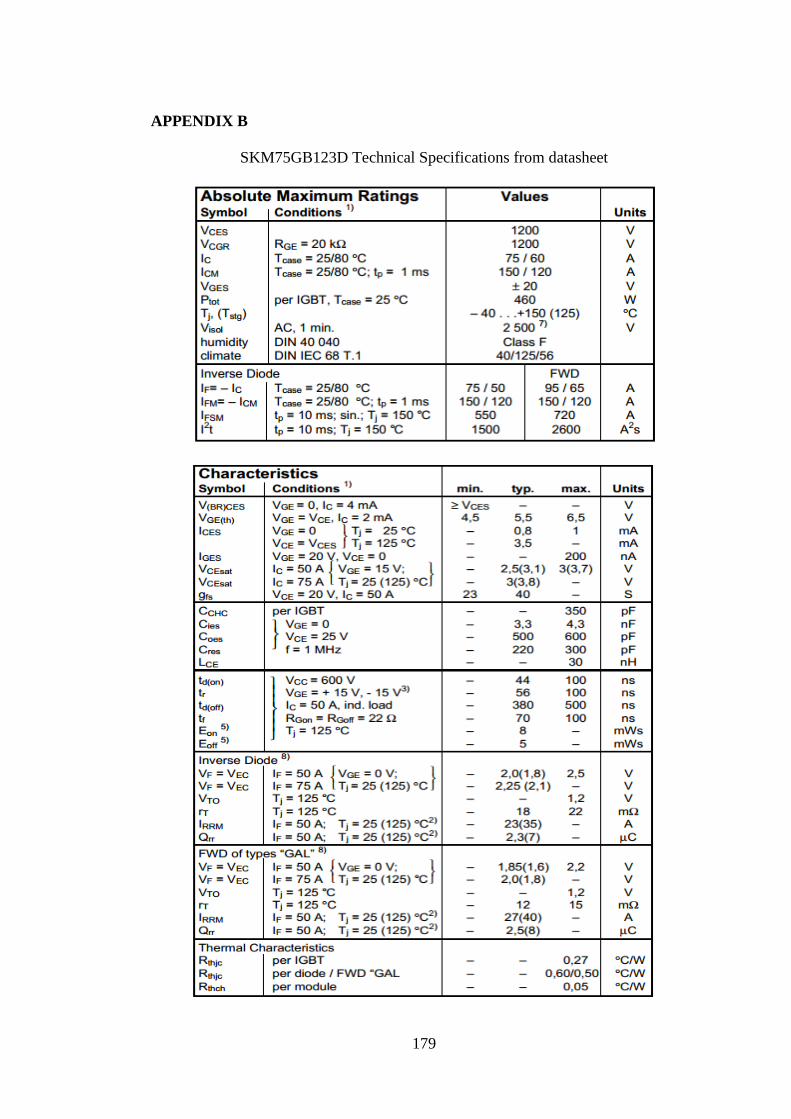
179
APPENDIX B
SKM75GB123D Technical Specifications from datasheet

180
ORCAD Model Editor Parameters for SKM75GB
.SUBCKT SKM75GB C G E
D_D1 E C DSEP8-12A
Z_Q1 C G E SKM75GB
*DEVICE=SKM75GB,NIGBT
* SKM75GB NIGBT model
* updated using Model Editor release 9.2.1 on 02/24/04 at 16:54
* The Model Editor is a PSpice product hem.
.MODEL SKM75GB NIGBT
+ TAU=117.55E-9
+ KP=10.139
+ AREA=25.000E-6
+ AGD=10.000E-6
+ WB=117.00E-6
+ VT=4.2231
+ MUN=3.5000E3
+ MUP=900
+ BVF=6.5380
+ KF=.5005
+ CGS=18.567E-9
+ COXD=37.349E-9
+ VTD=-5
*DEVICE=DSEP8-12A,D
* DSEP8-12A D model
* updated using Model Editor release 9.2.1 on 02/25/04 at 11:09
* The Model Editor is a PSpice product hem.
.MODEL DSEP8-12A D
+ IS=3.7288E-6
+ N=4.9950
+ RS=72.502E-3
+ IKF=999
+ CJO=1.0000E-12
+ M=.3333
+ VJ=.75
+ ISR=4.8113E-6
+ BV=1.2002E3
+ IBV=21.554E-3
+ TT=6E-8
.ENDS

181
APPENDIX C
LIST OF SYMBOLS
L Coupling inductance
R Internal resistance of coupling inductance
C DC link capacitor
av , bv , cv Supply voltages
ae , be , ce Terminal voltages of STATCOM
ai , bi , ci STATCOM currents
Lai , Lbi , Lci Load currents
Sai , Sbi , Sci Supply currents
aS , bS , cS Switching functions of each phase
dS , qS d, q components of switching functions
di , qi d, q components of STATCOM currents in SRF
dv , qv d, q components of terminal voltages
de , qe d, q components of STATCOM voltages
dci DC link current
dcv DC link voltage
Leakage Inductance
Synchronously angular velocity
Angular position
Load angle
P Active power
Q Reactive power
LQ Reactive power of load
Error signal
Kp, Ki Proportional and integral gains of PI controller.
EK , CEK Proportional and integral gains of digital PI controller.