w4a.002 3-d microcoils as a metamaterial …dr-walther.com/transducersproceedings11.pdf · 3-d...
TRANSCRIPT

3-D MICROCOILS AS A METAMATERIAL WITH ELECTRIC AND MAGNETIC RESPONSE
K. Kratt1, S. Waselikowski2, V. Badilita1,*, U. Wallrabe1, M. Walther2, J. G. Korvink1,3
1Department of Microsystems Engineering (IMTEK) 2Freiburg Materials Research Center (FMF)
3Freiburg Institute for Advanced Studies (FRIAS) University of Freiburg, Germany
ABSTRACT
This paper reports a terahertz metamaterial consisting of 3-D microcoils fabricated with an automatic wire bonder in a fully MEMS-compatible manner. The response of the system to an incident electromagnetic wave was characterized by terahertz time-domain spectroscopy (TDS) and by numerical simulations. Depending on the light polarization relative to the structure, fundamental and higher order electric or magnetic resonances were excited in the coils.
KEYWORDS
wire bonding, microcoil, metamaterial, terahertz INTRODUCTION
Metamaterials have attracted considerable interest in recent years due to the unprecedented control over their electromagnetic properties not attainable by naturally occurring materials. If a periodical collection of optically responding objects has size and spacing of considerably less than the wavelength of an electromagnetic wave, this group of single items can be viewed as homogeneous material at that wavelength, a “metamaterial”. Initially demonstrated at microwave frequencies, advances in structure miniaturization pushed the limits for applications of metamaterials towards optical wavelengths [1]. Possible applications are flux ducting in MRI [2], a “perfect” lens [3], a broadband circular polarizer [4], and an invisibility cloak [5].
As already mentioned, the dimensions of the periodical structures must be smaller than the targeted wavelength. As will be shown in this paper, we are able to fabricate arrays of structures with each having dimensions of 200 µm or less. Therefore, an electromagnetic wave in the low terahertz (THz) range (corresponding to a wavelength of several hundred micrometers to millimeters) is qualified to test the feasibility of our structures as a metamaterial.
Located at the interface between electronic and optical regimes, the terahertz range is particularly suited for the detailed investigation of metamaterial properties. Due to the moderate structure sizes and the availability of powerful characterization techniques, such as near-field microscopy or time-domain spectroscopy (TDS) [6], the terahertz regime provides the ideal testbed for investigating novel metamaterial structures and designs. The inherent scalability of metamaterial
structure allows the transfer of concepts to other frequencies.
To achieve a resonant response, metamaterials are typically built of sub-wavelength LC-oscillators consisting of an inductive element with inductance L and a capacitor with capacitance C. Consequently, their fundamental resonant frequency is
!
f0 =1
2" LC. (1)
Split-ring resonators (SRRs) are widely used LC-resonators and have been applied as metamaterial building blocks up to the high terahertz and infrared regime. An SRR is a two-dimensional conducting ring with a small gap whose dimensions define the resonant frequency. Recently, SRRs have been fabricated with MEMS technologies such as surface micromachining [7], multi-layer electroplating [8], and inkjet printing [9].
We fabricated 3-D LC-oscillator structures as shown in Figure 1. Gold pads are defined and serve as capacitors, whereas coils are wound with an automatic wire bonder around SU-8 posts as will be explained in more detail in the next section. The figure shows part of an array consisting of 10 x 10 coil-pad-structures with a periodicity of 700 !m.
Figure 1: Microscope picture of the manufactured metamaterial consisting of 10 x 10 coils. Each coil had a diameter of 200 !m, 2 windings, and a pitch of 50 !m. The coils were arranged with 700 µm periodicity. The inset shows an illustration of a single coil [14]. FABRICATION
Figure 2 shows a schematic of the process flow [10,11]. The substrate for our structures is made of glass. In a first step, a Cr/Au layer with 50/500 nm
W4A.002
978-1-4577-0156-6/11/$26.00 ©2011 IEEE Transducers’11, Beijing, China, June 5-9, 20112666

thickness was sputtered onto the wafer and structured with standard lithography to define pads. Pad dimensions, and therefore capacitor geometry, were 100 !m x 150 !m.
Figure 2: Schematic of the process flow. After gold pad patterning, thick SU-8 lithography is used to form the posts. Finally, the coils were made by wire bonding [10].
Secondly, high aspect ratio SU-8 processing with
UV-lithography formed the posts. The posts had a diameter of 200 !m with a height of about 650 !m. The posts were arranged with 700 !m periodicity in both, x- and y-direction.
In the final step, the coils were made. Starting from the gold pads, an automatic wire bonder wrapped insulated gold wire with a diameter of 25 !m around the posts. Wire bonders are usually used to connect a (semiconductor) chip with a leadframe in a 2-D trajectory. We have modified this trajectory to a 3-D motion around the pillars where the wire gets deformed plastically to the shape of the post. Each coil took about 200 ms to fabricate, resulting in a total bonding time for an array of 10 x 10 coils of about 20 s. We made coils with 2 windings each with a pitch between the windings of 50 !m. A snapshot of the bonding process is shown in Figure 3.
Figure 3: Snapshot during winding of coil [10].
EXPERIMENTS AND SIMULATION
The microcoil array was experimentally characterized by conventional THz-TDS based on the coherent emission and detection of free-space THz pulses from optically gated photoconductive antennas [12]. The amplitude transmission through the array was determined from measurements of the terahertz electric field transmitted under normal incidence through the sample and through the bare glass substrate as a reference.
In the simulation with COMSOL Multiphysics an individual microcoil structure was positioned in a 3-D simulation volume. The wire as well as the bond pads
were modeled as real metals with finite conductivity. A terahertz pulse was excited on one boundary and scattering boundary conditions have been imposed on the remaining sides of the simulation volume. Only excitation of a single coil was considered in the simulation since interaction between the coils can be neglected due to their large separation. In order to obtain a transmission spectrum from the simulation the terahertz electric field transient was sampled 1 mm behind the glass substrate. Division of the Fourier-transformed waveforms with and without the coil yields the transmission spectrum.
Figure 4 shows measured THz transmission spectra through the microcoil array for different excitation conditions and compares them to simulated data. Measurements were made with the sample plane normal to the beam for two orthogonal polarizations of the electric field relative to the microcoil structure (Ex and Ey) allowing to drive different resonances, which appear as characteristic transmission minima in the spectra. In both cases, excitation occurs via electric polarization of the structure, either across the gap between the bond pads (Figure 4(a), Ey excitation), or along the two parallel wire arms (Figure 4(b), Ex excitation). Alternatively, the structures can be magnetically excited if the incident magnetic field is oscillating along the coil axis (Bz excitation, dotted curve in Figure 4(a)). In this case, the same resonances are excited as for Ey excitation [13]. Note that pure magnetic excitation requires tilting of the probe by 90°. Our setup did not easily allow tilting, so that only electric excitation is shown experimentally. The fundamental mode (n = 1) had a frequency of 44 GHz, the highest order harmonic (n = 7) had a frequency of 524 GHz.
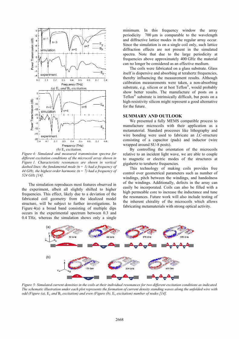
Figure 5 shows snapshots of the simulated electric current vectors for the resonance frequencies. The size of the arrows scales with the absolute value of current and the color indicates clockwise (blue) or anti-clockwise (red) current flow. The illustration under each plot sketches the corresponding current density standing wave pattern forming along the unwound wire. For Bz excitation (or similarly Ey excitation) only modes with an odd number of nodes are excited. These magnetic modes are associated with circulating currents in the ring forming the coil, resulting in strong magnetic moments. In contrast, for Ex excitation only even modes are formed: counter-propagating currents in the coil interfere destructively, so that only an electric dipole is formed in the far-field [14].
DISCUSSION
Due to the moderate size, the resonances were in the low terahertz range. If higher resonant frequencies are required, the post diameter (to decrease the inductance) or the pads size (to decrease the capacitance) must be decreased. Further miniaturization is possible down to a post diameter of about 100 µm, e. g. with posts made of PMMA by X-ray lithography [15].
2667
(a) Ey and Bz excitation.
(b) Ex excitation.
Figure 4: Simulated and measured transmission spectra for different excitation conditions of the microcoil array shown in Figure 1. Characteristic resonances are shown in vertical dashed lines: the fundamental mode (n = 1) had a frequency of 44 GHz, the highest order harmonic (n = 7) had a frequency of 524 GHz [14].
The simulation reproduces most features observed in
the experiment, albeit all slightly shifted to higher frequencies. This effect, likely due to a deviation of the fabricated coil geometry from the idealized model structure, will be subject to further investigations. In Figure 4(a) a broad band consisting of multiple dips occurs in the experimental spectrum between 0.3 and 0.4 THz, whereas the simulation shows only a single
minimum. In this frequency window the array periodicity !700 !m is comparable to the wavelength and diffractive lattice modes in the regular array occur. Since the simulation is on a single coil only, such lattice diffraction effects are not present in the simulated spectra. Note that due to the large periodicity at frequencies above approximately 400 GHz the material can no longer be considered as an effective medium.
The coils were fabricated on a glass substrate. Glass itself is dispersive and absorbing at terahertz frequencies, thereby influencing the measurement results. Although calibration measurements were taken, a non-absorbing substrate, e.g. silicon or at best Teflon®, would probably show better results. The manufacture of posts on a Teflon® substrate is intrinsically difficult, but posts on a high-resistivity silicon might represent a good alternative for the future.
SUMMARY AND OUTLOOK
We presented a fully MEMS compatible process to manufacture microcoils with their application as a metamaterial. Standard processes like lithography and wire bonding were used to fabricate an LC-structure consisting of a capacitor (pads) and inductor (wire wrapped around SU-8 posts).
By controlling the orientation of the microcoils relative to an incident light wave, we are able to couple to magnetic or electric modes of the structures at gigahertz to terahertz frequencies.
This technology of making coils provides free control over geometrical parameters such as number of windings, pitch between the windings, and handedness of the windings. Additionally, defects in the array can easily be incorporated. Coils can also be filled with a high permeable core to increase the inductance and tune the resonances. Future work will also include testing of the inherent chirality of the microcoils which allows fabricating metamaterials with strong optical activity.
Figure 5: Simulated current densities in the coils at their individual resonances for two different excitation conditions as indicated. The schematic illustration under each plot represents the formation of current density standing waves along the unfolded wire with odd (Figure (a), Ey and Bz excitation) and even (Figure (b), Ex excitation) number of nodes [14].
2668

ACKNOLEDGEMENTS Stefan Waselikowski and Markus Walther
acknowledge financial support by the DFG through Grant No. WA 2641 and by the Baden-Württemberg Ministry for Science and Arts through the Research Seed Capital !“RiSC”" program. Kai Kratt and Vlad Badilita acknowledge funding from the EU NEST Project No. 028533 (“microMR”). REFERENCES [1] C. M. Soukoulis, S. Linden, Martin Wegener,
“Negative refractive index at optical wavelengths”, Science, vol. 315, pp. 47-49, 2007.
[2] M. C. K. Wiltshire, J. B. Pendry, D. J. Larkman, D. J. Gilderdale, D. Herlihy, I. R. Young et al., “Geometry preserving flux ducting by magnetic metamaterials”, in Proceedings of ISMRM, Toronto, Canada, p. 713, 2003.
[3] J. B. Pendry, “Negative refraction makes a perfect lens”, Physical Review Letters, vol. 5, 2000.
[4] J. K. Gansel, M. Thiel, M. S. Rill, M. Decker, K. Bade, V. Saile et al., “Gold helix photonic metamaterial as broadband circular polarizer”, Science, vol. 325, pp. 1513-1515, 2009.
[5] T. Ergin, N. Stenger, P. Brenner, J. B. Pendry, M. Wegener, “Three-dimensional invisibility cloak at optical wavelengths”, Science, vol. 28, pp. 337-339, 2010.
[6] A. Bitzer, H. Merbold, A. Thoman, T. Feurer, H. Helm, M. Walther, “Terahertz near-field imaging of electric and magnetic resonances of a planar metamaterial”, Optics Express, vol. 17, pp. 3826-3834, 2009.
[7] H. Tao, A. C. Strikwerda, K. Fan, W. J. Padilla, R. D. Averitt, X. Zhang, “Terahertz metamaterials with simultaneously negative electric and magnetic resonance responses based on bimaterial pop up structures”, in Proceedings of MEMS, Sorrento, Italy, pp. 108-111, 2009.
[8] K. Fan, A. C. Strikwerda, H. Tao, R. D. Averitt, X. Zhang, “3D stand- up metamaterials with a purely magnetic resonance at terahertz frequencies”, in Proceedings of MEMS, Hong Kong, China, pp. 843-846, 2010.
[9] M. Walther, A. Ortner, H. Meier, U. Löffelmann, P. J. Smith, J. G. Korvink, “Terahertz metamaterials fabricated by inkjet printing”, Applied Physics Letters, vol. 95, 251107, 2009.
[10] K. Kratt, V. Badilita, T. Burger, J. G. Korvink, U. Wallrabe, “A fully MEMS-compatible process for 3D high aspect ratio micro coils obtained with an automatic wire bonder”, Journal of Micromechanics and Microengineering, vol. 20, 015021, 2010.
[11] V. Badilita, K. Kratt, N. Baxan, M. Mohammadzadeh, T. Burger, H. Weber et al., “On-chip three dimensional microcoils for MRI at the microscale”, Lab on a Chip, vol. 10, pp. 1387-1390, 2010.
[12] D. Grischkowsky, S. Keiding, M. van Exter, Ch. Fattinger, “Far-infrared time-domain spectroscopy with terahertz beams of dielectrics and semiconductors”, Journal of the Optical Society of America B, vol. 7, pp. 2006-2015, 1990.
[13] N. Katsarakis, T. Koschny, M. Kafesaki, E. N. Economou, C. M. Soukoulis, “Electric coupling to the magnetic resonance of split ring resonators”, Applied Physics Letters, vol. 84, 2943, 2004.
[14] S. Waselikowski, K. Kratt, V. Badilita, U. Wallrabe, J. G. Korvink, M. Walther, “Three-dimensional microcoils as terahertz metamaterial with electric and magnetic response”, Applied Physics Letters, vol. 97, 261105, 2010.
[15] K. Kratt, V. Badilita, T. Burger, J. Mohr, M. Börner, J. G. Korvink et al., “High aspect ratio PMMA posts and characterization method for micro coils manufactured with an automatic wire bonder”, Sensors and actuators A: Physical, vol. 156, pp. 328-333, 2009.
CONTACT
Dr. V. Badilita, Laboratory for Microactuators, Department of Microsystems Engineering – IMTEK, University of Freiburg, Germany, Tel: +49-761-203-7435; Fax: +49-761-203-7439; E-mail: [email protected].
2669