wang, liqiu (2013) quantitative three dimensional atomic...
TRANSCRIPT

Glasgow Theses Service http://theses.gla.ac.uk/
Wang, LiQiu (2013) Quantitative three dimensional atomic resolution characterisation of non-stoichiometric nanostructures in doped bismuth ferrite. PhD thesis. http://theses.gla.ac.uk/4364/ Copyright and moral rights for this thesis are retained by the author A copy can be downloaded for personal non-commercial research or study, without prior permission or charge This thesis cannot be reproduced or quoted extensively from without first obtaining permission in writing from the Author The content must not be changed in any way or sold commercially in any format or medium without the formal permission of the Author When referring to this work, full bibliographic details including the author, title, awarding institution and date of the thesis must be given

Quantitative Three Dimensional
Atomic Resolution Characterisation
of Non-stoichiometric Nanostructures
in Doped Bismuth Ferrite
LiQiu Wang
Presented as a thesis for the degree of Ph.D. at the
school of Physics and Astronomy, University of Glasgow
January 2013
© L.Q. Wang 2013

i
Abstract
Over the last decade, the lead-free, environmentally-friendly multiferroic
material, BiFeO3 (BFO), has once again received tremendous attention from researchers,
not only for its fundamental properties, but also for its potential applications such as
novel devices that can be written by an electric field and read by a magnetic field.
However, one of the most important limitations for applications is the high leakage
current in pure materials. Doping has proved to be an effective way to reduce the
leakage current caused by the electron hopping between Fe2+
and Fe3+
. In this work, a
series of Nd3+
and Ti4+
co-doped BFO compositions have been studied using a
combination of atomic resolution imaging and electron energy loss spectroscopy in
STEM, especially concentrating on nanostructures within the Bi0.85Nd0.15Fe0.9Ti0.1O3
composition, as nanostructures can play an important role in the properties of a crystal.
Two types of novel defects – Nd-rich nanorod precipitates and Ti-cored anti-phase
boundaries (APBs) are revealed for the first time. The 3D structures of these defects
were fully reconstructed and verified by multislice frozen phonon image simulations.
The very formation of these defects was shown to be caused by the excess doping of Ti
into the material and their impact upon the matrix is discussed. The nanorods consist of
8 atom columns with two Nd columns in the very center forming the Nd oxide. Density
functional theory calculation reveals that the structures of the nanorod and its
surrounding perovskites are rather unusual. The Nd in the core is seven coordinated by
oxygen while the coordination of B site Fe3+
at its surroundings are just five-coordinated
by oxygen due to the strain between the nanorod and the surrounding perovskite. The
APB is nonstoichiometric and can be treated as being constructed from two main
structural units - terraces and steps. Within the terraces, Ti4+
occupy the centre of the
terrace with Ti/Fe alternately occupying either side of the terrace. As for the step, this is
constructed from iron oxide alone with a structure similar to -Fe2O3, and Ti is
completely absent. Quantitative analysis of the structure shows the APB is negatively
charged and this results in electric fields around the APBs that induce a local phase
transformation from an antiferroelectric phase to a locally polarised phase in the
perovskite matrix. Based on this thorough investigation of these defects, a new ionic
compensation mechanism was proposed for reducing the conductivity of BiFeO3 without
the complications of introducing non-stoichiometric nanoscale defects.

ii
Acknowledgements
I am very grateful for having the opportunity to be able to study in MCMP group
under the supervision of Dr Ian MacLaren and Prof. Alan Craven. Their guidance,
patience and encouragement have been greatly appreciated. Their attitude toward
research has set up a very good example for me, which will guide me through my career
whatever I will do in the future. Their caring, thoughtful, kind personality will never be
forgotten. I am also very grateful for EPSRC founded me through my study. I would
also like to give lots of thanks to Prof. Ian M Reaney who generously provided those
precious samples and gave many fruitful and stimulating discussions and advice. The
support from Dr Bernhard Schaffer and Dr Quentin Ramasse and other services at
SuperSTEM have been incredible. To all the staff at SuperSTEM, I must say a big
“thank you” to all of you. I am also very appreciated to Dr S. M. Selbach and Prof N.
Spaldin for their wonderful calculation work.
The friendly environment provided by the MCMP group has been wonderful.
Colloquiums organized by Dr Donald MacLaren have been a great benefit to my study.
Technical staff is all very supportive. Especially, I would like to thank Dr Sam
McFadzean for his useful discussions regarding TEM, and Mr Brian Miller who is
missed very much for teaching and making TEM samples so patiently. I am also
indebted to Dr Damien McGrouther for his invaluable help.
I would also like to say thank you all to other staff within the MCMP group and
all the colleagues who stayed together in room 402 and 413 for making my study time so
enjoyable and memorable.
A big thanks and a big hug should also be given to my Mum who is fighting for
her lung cancer at the last stage. Without her support and encouragement and her wise
guidance in my early years, this thesis wouldn’t be made possible. I am also in debt to
my sisters and brothers-in-law for looking my mum when she was ill. My daughter has
contributed a lot to my thesis by being behaved very well, I would say, so a big hug and
kiss to her. At last but not the least, my husband deserves more than thanks for being so
thoughtful and so supportive whenever I needed it.

iii
Declaration
This thesis has been written by myself and details the research I have carried out within
the MCMP group under the supervision of Dr Ian MacLaren and Prof. Alan Craven in
the school of Physics and Astronomy at the University of Glasgow from 2009 - 2013.
The work described is my own except where otherwise stated.
This thesis has not previously been submitted for a higher degree.
Some parts of the work have been published in the following papers:
I. MacLaren, L. Q. Wang, B. Schaffer, Q. M. Ramasse, A. J. Craven, S. M. Selbach, N. A.
Spaldin, S. Miao, K. Kalantari, I. M. Reaney, (2013) Novel Nanorod Precipitate Formation in
Neodymium and Titanium Codoped Bismuth Ferrite, Advanced Functional Materials,
Volume 23, Issue 2, 683-689.
I. M. Reaney, I. MacLaren, L.Q. Wang, B. Schaffer, A. J. Craven, K. Kalantari, I. Sterianou, S.
Miao, S. Karimi, and D. C. Sinclair, (2012) Defect chemistry of Ti-doped antiferroelectric
Bi0.85Nd0.15FeO3, Applied Physics Letters, 100, 182902.
L. Q. Wang, B. Schaffer, A. Craven, I. MacLaren, S. Miao and I. Reaney, (2011) Atomic Scale
Structural and Chemical Quantification of NonStoichiometric Defects in Ti and Bi Doped
BiFeO3. Microscopy and Microanalysis 17 (Suppl. 2, 1896-1897) doi:10.1017/
S143192761101035X.
L. Q. Wang, B. Schaffer, I. MacLaren, S. Miao, A. J. Craven and I. M. Reaney, (2012) Atomic
scale structure and chemistry of anti-phase boundaries in (Bi0.85Nd0.15)(Fe0.9Ti0.1)O3
ceramics, Journal of Physics: Conference Series 371, 012036.
L. Q. Wang, B. Schaffer, I. MacLaren, S. Miao, A. J. Craven and I. M. Reaney, (2012) Atomic-
resolution STEM imaging and EELS-SI of defects in BiFeO3 ceramics co-doped with Nd
and Ti, Journal of Physics: Conference Series 371, 012034.

iv
Contents
Abstract i
Acknowledgements ii
Declaration iii
Contents iv
List of figures and tables viii
1 Introduction 1
1.1 Multiferroics 2
1.2 General Properties of Multiferroics 3
1.2.1 Ferroelectricity 3
1.2.1.1 Crystal symmetry with respect to ferroelectricity 3
1.2.1.2 Curie temperature and phase transitions 5
1.2.1.3 Domain and domain wall in ferroelectrics 6
1.2.1.4 Hysteresis 7
1.2.2 Ferromagnetism 8
1.2.3 Magnetoelectric (ME) effect - coupling between
ferroelectricity and (anti-) ferromagnetism 10
1.3 Properties of BFO 11
1.3.1 Perovskites – ABO3 corner sharing octahedra 11
1.3.2 Properties of BiFeO3 (BFO) 12
1.4 Motivation of This Study 14
2 Instrumentation and Sample Preparation 21
2.1 Overview of The Microscopes Used in This Work 22
2.1.1 The FEI Tecnai T20 22
2.1.2 SuperSTEM2 27
2.1.3 Electron lenses and aberrations 29

v
2.1.3.1 Electromagnetic lenses 29
2.1.3.2 Defects of electromagnetic lenses - aberrations 31
2.1.3.2.1 Geometric aberrations 31
2.1.3.2.2 Chromatic aberration 35
2.1.4 Image resolution and aberration correction 36
2.1.4.1 Spherical aberration limited image resolution 39
2.1.4.2 Chromatic aberration limited image resolution 40
2.1.4.3 Diagnosis of spherical aberration – the electron
Ronchigram 41
2.2 Imaging 43
2.2.1 Image contrast 43
2.2.2 Bright-field and ark-field diffraction contrast imaging –
coherent imaging 43
2.2.3 High angle annular dark field (HAADF) imaging with STEM –
incoherent imaging 45
2.3 Electron Energy-loss Spectroscopy 47
2.3.1 Interactions of electrons with sample 47
2.3.1.1 Elastic scattering 47
2.3.1.2 Inelastic scattering 48
2.3.2 Electron energy-loss spectrometer 48
2.3.3 EELS 50
2.3.4 Spectrum – imaging 52
2.4 Sample Preparation 54
2.4.1 Ceramic preparation 54
2.4.2 Specimens for TEM 54
3 Computational software related to data analysis 59
3.1 Introduction 59
3.2 Principal Component Analysis (PCA) 59
3.3 Drift Correction via The Statistically Determined Spatial Drift (SDSD)
Method 64

vi
3.4 iMtools 66
3.5 Distortion Correction and Primary Model Development 66
3.6 Image Simulation 67
3.6.1 Multislice algorithm 68
3.6.2 Frozen phonon method 70
3.6.3 QSTEM 71
3.7 Density Functional Theory 72
4 Characterisation of nanorod precipitates 77
4.1 Introduction 77
4.2 TEM Imaging of The Nanorods and Their Connection to The Domain
Structure of Bi0.85Nd0.15Fe0.9Ti0.1O3 78
4.3 Quantitative Analysis of Atomic Resolution STEM Imaging and
Chemical Mapping of The Nanorods from Bi0.85Nd0.15Fe0.9Ti0.1O3
sample 80
4.3.1 Quantitative analysis of the atom positions from HAADF STEM
images 80
4.3.2 Chemical mapping of the nanorods from the top view 85
4.3.3 Imaging of the nanorods from the side view 91
4.3.4 Chemical mapping of the nanorods from the side view 92
4.4 The 3-Dimensional Structure of The Nanorods 93
4.4.1 The primary 3D model of the structure of the nanorods 93
4.4.2 Optimum of the 3D structure model by DFT 94
4.4.3 Structural model confirmation by multislice image simulation-
QSTEM 97
4.4.4 Summary of the features for the nanorod structural model 99
4.5 Properties of The Nanorods and Their Effects on The Perovskite
Matrix 100
4.5.1 Strain interactions with the matrix, spontaneous alignment
and domain pinning 100
4.5.2 Electronic properties of the nanorods 101

vii
4.5.3 Doping level effect on the nanorods and the perovskite
matrix 102
4.6 Conclusions 104
5 Novel anti-phase boundaries 108
5.1 Introduction 108
5.2 About The Novel APB 109
5.3 Quantitative Analysis of The APB - Terrace Part 111
5.3.1 Structural and chemical information about terrace 111
5.3.2 Creation of structural model and simulation results 113
5.4 Quantitative Analysis of The APB - Step Part 117
5.5 The Effect of The APB with Its Adjacent Matrix 122
5.6 Conclusions 125
6 Summary and Future Work 130
6.1 Summary 130
6.2 Future Work 131

viii
List of Figures and Tables
List of Figures
Figure 1.1: A schematic diagram of relative permittivity of BaTiO3 changes with the
phase transitions.
Figure 1.2: A schematic diagram of Polarization vs. Electric Field (P-E) hysteresis
loop for a typical ferroelectric crystal.
Figure 1.3: Four types of magnetic dipole ordering in magnetic materials.
Figure 1.4: (a) 3D network of corner sharing octahedra of O2-
ions (left) (b) A cubic
ABO3 perovskite-type unit cell (right).
Figure 1.5: A schematic hexagonal structure of BFO with pseudocubic unit cell
(doubled perovskite unit cell).
Figure 1.6: Preliminary phase diagram for Bi1-xNdxFeO3 derived using a
combination of XRD, DSC, Raman, and TEM data.
Figure 2.1: A schematic diagram of FEI Tecnai T20 column consisting of
illumination system (electron source, C1, C2/ C2 aperture), magnification
system(objective lens, diffraction lens, intermediate lens and projector
lenses, and objective, selected area apertures), SIS camera and GIF.
Figure 2.2: A principal ray diagram of FEI T20 showing the specimen being
illuminated by a parallel beam and a bright-field image will be formed as
the final image.
Figure 2.3: a) A schematic diagram of main components of the column of the Nion
UltraSTEM 100 with an on-site picture of SuperSTEM2 (inserted). b) A
principal ray diagram of SuperSTEM2 showing electrons are formed into
a fine probe and is focused on the specimen after the aberration corrector.
Figure 2.4: A schematic section of a polepiece showing its structure and two paths of
the electron ray due the radial component Br of the magnetic field.

ix
Figure 2.5: A schematic diagram showing spherical aberration - a point object is
imaged as a disk with radius rs≈Csα3 due to spherical aberration that
causes the off-axis rays are not focused at the same point F as those
paraxial rays.
Figure 2.6: Schematic diagram of axial astigmatism. Rays leaving an axial image point,
focused by a lens (with axial astigmatism) into ellipses centred around Fx
if they travel in x-z plane or Fy if they travel in y-z plane, with long axis
normal to the plane they travel, or into a circle of smallest radius - the
disc of least confusion.
Figure 2.7: Schematic diagram of coma aberration which causes an off-axis object
point imaged as comet shaped. Rays travel through the peripheral field of
the lens with an incident angle are focused at different point from those
travel parallel to the optic axis or through the centre.
Figure 2.8: Schematic diagram shows electrons with different energies being focused
at different planes due to chromatic aberration.
Figure 2.9: A schematic diagram of a focused beam on the specimen in CTEM
showing the definition of convergence semi-angle α, which is determined
by the condenser lens and condenser aperture and collection semi-angle
β, which is determined by the spectrometer entrance aperture.
Figure 2.10: A schematic plot of sinχ(α) versus α showing the contrast transfer as a
function of spatial frequency with uncorrected TEM. The first crossover
indicating the maximum allowable spatial frequency for intuitive image
interpretation. Es is the envelope of spatial coherence of the source and Et
is the chromatic aberration envelope.
Figure 2.11: A typical electron Ronchigram with two characteristic rings of infinite
magnification appear around the sample shadow image showing spherical
aberration.
Figure 2.12: Ray diagrams showing how to form BF and DF images. A) a BF image
formed from direct beam. B) a DF image formed from a specific
diffracted beam by displacing the objective aperture. C) a DF image

x
formed by tilting the incident beam so that the scattered beam is on axis.
The area selected by the objective aperture is shown on the viewing
screen below each ray diagram.
Figure 2.13: A SAD pattern showing [001] orientation and its related DF image
showing the grain boundaries clearly as marked by the light blue line
(BiFeO3 co-doped with 10% Nd, 3% Ti).
Figure 2.14: Schematic diagram shows relative positions of different detectors with
semi-angles θ1 < 10 mrad (BF), 10 mrad < θ2 < 50 mrad (MAADF),
θ3 > 50 mrad (HAADF).
Figure 2.15: Schematic diagram showing interactions of direct beam with specimen.
Figure 2.16: EELS showing different energy loss regions of spectrum. A) a spectrum
showing ZLP as marked in orange rectangle and the rest of the peaks are
Plasmon caused by multiple excitation; Plasmon peaks are rather high
because the sample is very thick. B) a spectrum showing core-loss region
with characteristic ionization edges labelled .
Figure 2.17: A schematic diagram of spectrum imaging technique, which can be used
for quantitative analysis.
Figure 2.18: Images of same silicon sample taken at same conditions of TEM. a)
Before gentle milling. b) After gentle milling.
Figure 3.1: Comparison of spectra before and after PCA: left is the original spectrum;
right is the spectrum after PCA was applied
Figure 3.2: An example of the screen plot, showing the correlation between log
eigenvalue and components. Significant features are represented by those
exponentially decreased principal component, experimental random noise
are represented by the straight line in the scree plot. 10 components
reconstructed spectrum image showing the random back ground noise has
been greatly reduced.
Figure 3.3: Selected pairs of the loading spectra and the corresponding score images
of the components showing significant features are represented by those

xi
exponentially decreased principal components in the scree plot of Figure
3.2.
Figure 3.4: (a) One slice from a series of images taken using a dwell time of
5μs/pixel; (b) A sum of the image series after spatial drift correction.
Figure 3.5: Interface of iMtools and fitted peak image (top-right) from the SDSD
corrected HAADF image (left) together with corresponding coordinates
list.
Figure 3.6: A chart of the corresponding defect in Figure 3.5 plotted with Excel
using the coordinations (x, y) extracted by iMtools.
Figure 4.1: a) Dark field image of one area examined by HRSTEM; diffraction
patterns insets show the crystal orientation to either side of the domain
boundary, which appears as a bright diagonal line. b) HAADF image of
nanorod precipitates in an end-on orientation.
Figure 4.2: A typical procedure for linear distortions correction, including shifting
peak positions to zero, rotation correction, shear correction and
magnification correction.
Figure 4.3: HAADF images showing six defects used for quantifying atomic
positions. Scale bars can be worked out by the distance between two
nearest bright A-site spots of the bulk matrix, which is about 3.965Å.
Figure 4.4: Corrected A-site positions for six defects: a) the positions for each of the
six defect images, each in a different colour, together with a symmetry
markers for the proposed 2mm plane symmetry of the defect; b) averages
for each position after averaging all symmetrically equivalent positions to
generate each data point, error bars are 3σ to make them clearly visible.
Figure 4.5: Processing steps involved in creating the maps shown in Figure 4.6: the
initial maps are created from a PCA analysed spectrum image using the
first 20 components, these are then normalised by division by the carbon
map shown to try to normalise them to the total signal entering the
spectrometer. Finally, maps are cleaned up by the application of a low
pass filter.

xii
Figure 4.6: Quantitative imaging and electron energy loss elemental mapping of the
nanorods in an end-on orientation; a) HAADF image formed by summing
46 drift-corrected short acquisitions of one area. b) – e) elemental maps
created from a EELS-SI of one such nanorod: b) Fe map; c) Nd map; d)
Ti map; e) RGB map created where red represents Fe, green represents
Nd and blue represents Ti; f) O K-edge EELS spectra from the nanorod
core, outside the nanorod core and a Nd2O3 spectrum for reference; g)
MLLS fit coefficient map for the O-K edge shape for bulk perovskite; h)
MLLS fit coefficient map for the O-K edge shape for the Nd2O3 edge
shown in f).
Figure 4.7: a) Elemental maps for another defect with similar results as in Figure 4.6.
b) elemental maps for a defect but overlapped with normal BFO crystal
matrix. HAADF images presented in both a) and b) were acquired
simultaneously with EEL-SI.
Figure 4.8: Side views of some different nanorod precipitates (in all cases nanorods
are indicated by yellow arrows): a) and b) lower magnification MAADF
images, showing strain around the precipitates; c)-f) HAADF images
formed by repeat scanning, alignment and summation of multiple scans.
Figure 4.9: Quantitative imaging and electron energy loss elemental mapping of the
nanorods in side-on orientation; a) HAADF image of one such nanorod
formed by summing 27 drift-corrected short acquisitions, pairs of Nd
atoms along the beam direction are indicated by yellow arrows. b)-e)
elemental maps created from a EELS-SI of one such nanorod, the
nanorod lies between the arrows in all maps: b) Fe map; c) Nd map; d) Ti
map; e) RGB map created where red represents Fe, green represents Nd
and blue represent Ti.
Figure 4.10: The initial model of nanorods with all the B-sites atoms 6 coordinated.
Figure 4.11: Regions of the supercell model used for plotting local DOS in Figure
4.12; blue: matrix region; red: nanorod region and green: (outside red):
interface region.

xiii
Figure 4.12: Atomic structure models after DFT structural relaxations in end-on
orientation and their correlated DOS; a) the model with five-coordinated
Ti towards the Nd nanorod columns; b) is the model with six-coordinated
Ti away from the Nd nanorod columns; c) DOS from model with five-
coordinated Ti; d) DOS from model (b) with six-coordinated Ti.
Figure 4.13: HAADF image simulations for this model compared to real images: a)
end-on image of a nanorod; b) simulation of a nanorod extending through
the entire 40 cell thickness of the crystal; c) image of the overlap between
a defect and perfect crystal; d) simulation of 10 unit cells of nanorod on
the entrance surface followed by 30 unit cells of perfect perovskite
BiFeO3; e) image of another overlap between a nanorod and perfect
crystal; f) simulation of 10 cells of perfect perovskite overlaying 20 cells
of nanorod, followed by 10 more cells of perfect crystal; g) side-on view
of a nanorod (detail from the same image as used in Figure 4.9a); h)
simulation of an image of a nanorod lying right at the entrance surface of
the crystal viewed along the a-axis (as shown in Figure 4.12), followed
by perfect crystal, with a total thickness of 30 unit cells.
Figure 4.14: MAADF image of BNFT-12.5_3 sample with inserted HAADF image,
showing the coexistence of end-on (marked with pink colour) and side-on
(marked with yellow-green colour) views of the nanorods.
Figure 4.15: MAADF images of BNFT-10_3 sample, showing the coexistence of end-
on (marked with pink colour) and side-on (marked with yellow-green
colour) view of the nanorods, but the length of side-on defects are quite
short; inserted are HAADF images showing the coexistence of side-on
views of two orientations.
Figure 4.16: MAADF images showing the doping level effect on density and strain
with samples of BNFT-10_3, a); BNFT-12.5_3 ,b); BNFT-15_10, c).
Figure 5.1: a) DF image with SAD pattern showing an area with two darker ribbons
running cross the sample; b) HAADF image reveals the two darker
ribbons are actually APBs consisting of terrace parts with varied length
and steps, and the dark spots between the two ribbons in DF image are

xiv
corresponding the nanorods in between the two APBs. The half unit cell
shifting cross the boundary is marked by the green lines; horizontal shift
of one perovskite unit cell at the steps is indicated by blue lines.
Figure 5.2: Atomic resolution STEM images and EELS maps of the APB (terrace
part) along the first projection; the colour scales are shown for the false
colour images and the same scale was used for both HAADF and BF
images. Insets of the simulated images are overlaid on the experimental
images using exactly the same contrast scale. The EELS maps for
individual images show the full contrast range, whereas the contrast has
been enhanced to remove background intensity and thus to enhance
visibility of the main atomic columns in the RGB image.
Figure 5.3: Elemental maps from two other areas showing the chemistry similarity
of the APBs (terrace part).
Figure 5.4: HAADF image and EELS maps of the antiphase boundary along the
second (perpendicular) projection. An inset of a simulated image is
overlaid on the HAADF image using exactly the same contrast scale. The
EELS maps for individual images show the full contrast range, whereas
the contrast has been enhanced to remove background intensity and thus
to enhance visibility of the main atomic columns in the RGB image.
Figure 5.5: QSTEM simulation results from different models. a) From a model with
no oxygen in the unit occupies the position corresponding the very bright
spot in BF image and very dark place in HAADF image. b) From a model
with only one position in the unit is fully occupied by oxygen, which
shows bright spot as circled, and the other one is half occupied by
oxygen. c) From a model with both positions in the unit occupied by
oxygen, resulting bright spots are circled as well. d) From the final model
with 4 mrad-tilted angle. f) The same BF image in grey scale as was used
in Figure 5.2 for the comparison with image (d). The blue parallelogram
marks the two close pairs of oxygen with contrast difference between
them.

xv
Figure 5.6: 2D visions from the final model of APB (the terrace part) with purple
represents Bi atoms, red represents oxygen atoms, light blue for Ti and
brown for Fe. a) Top view of the model. b) Tilted side view of the model
to show the alternative B-site occupancies of Ti/Fe on either side of the
terrace.
Figure 5.7: HAADF image (left) with two steps and corresponding BF image (right);
For further comparison, the lower step is magnified and displayed
together with the simulation results.
Figure 5.8: Elemental maps from EELS of different areas as indicated by
simultaneously recorded HAADF images (in green framed). Colour
indications are the same as before: red for Fe, blue for Ti and green for
HAADF.
Figure 5.9: Co-efficiency fitting maps corresponding to the O K-edge reference
spectra as displayed below and Fe ELNEFS. (Green colour represents the
spectrum from the perovskite and red represents the spectrum from the
step).
Figure 5.10: Top view of the 3D structural model for APB (step part) with main
feature of the step marked with bright green parallelogram.
Figure 5.11: a) out-of-plane lattice parameter dependence on distance from the
boundary; b) local polarisation dependence on distance from the
boundary.
Figure 5.12: The repeat units for the calculation of charge densities for terrace (a) and
for step (b); purple for Bi, brown for Fe, light-blue for Ti and red for O.
List of Tables
Table 1.1: Point groups for the seven crystal systems.
Table 2.1: Aberration coefficients and their corresponding conventional names.

xvi
Table 3.1: Steps for simulations of STEM images of thick specimen.
Table 4.1: Averaged atomic positions for the defect after reduction to 2mm
symmetry.
Table 4.2: Typical Mapping parameters using in creating the maps.

Chapter 1 Introduction
1
Chapter 1 Introduction
Multiferroics (for a definition see section 1.1) have been an intriguing study field
in recent years because of their fascinating phenomena in physics and wide ranging
applications like high-sensitivity ac magnetic field sensors and electrically tunable
microwave devices such as filters, oscillators and phase shifters (in which the ferri-,
ferro- or antiferro-magnetic resonance is tuned electrically instead of magnetically). One
of the most appealing aspects of multiferroics is the so-called magnetoelectric (ME)
effect, which means ferroelectric polarization can be controlled by a magnetic field and,
conversely, magnetization can be manipulated by an electric field. This effect could be
exploited for the development of new devices including novel spintronics and spin
valves with electric field tuneable functions, or even non-volatile magnetic storage bits
which can combine the advantages of FeRAMs (ferroelectric random access memories)
and MRAMs (magnetic random access memories). However, there are not many
materials that exhibit a strong ME effect - almost all of them are antiferromagnetic or
weak ferromagnets [Mariya 1960, Hill 2000]. Regarding the weak ferromagnetism, there
are two mechanisms. One originates from anisotropic superexchange interactions, and
materials with this type of weak ferromagnetism normally have higher Néel
temperatures. The other is from single spin anisotropy energy and materials with this
type of magnetism tend to have low Néel temperatures [Mariya 1960], which limits their
applications. As for BiFeO3 (BFO), it has the advantages desired by device designers
with both Curie temperature (~830ºC) and Néel temperature (~370ºC) well above room
temperature. Furthermore, the origin of ferroelectricity is different from that of the
antiferromagnetism. The former is caused by the structural distortion introduced by the
6s lone pair electrons of A-site Bi and the later is from the transition metal d-electrons
on the B-site iron. From this aspect, we might be able to manipulate the ferroelectricity
and magnetism separately by substituting A and/or B-site atoms. In this thesis,
investigations to a series of Nd and Ti co-doped BFO samples on nanoscale structures
were carried out. The detailed rationale for these studies will be discussed in more detail
in this chapter (section 4), as well as in further detail in chapters 4 and 5. This thesis is
structured in the following manner: this chapter will briefly review the current state of
knowledge on multiferroics with specific reference to bismuth ferrite and other

Chapter 1 Introduction
2
perovskite multiferroics, and will serve as an introduction to the whole thesis. Chapter 2
will serve as giving an overview of transmission electron microscopy (TEM) and
scanning transmission electron microscopy (STEM). Chapter 3 will detail the data
analysis and computer simulation approaches used in the research described in the
following two chapters. Chapter 4 will then detail the atomic scale structure and
chemistry of nanorod precipitates in Ti, Nd doped bismuth ferrite, together with their
dependence on material composition. Chapter 5 will detail the atomic scale structure,
chemistry and dielectric effects of antiphase boundaries in the same material. Chapter 6
then summarises the conclusions of these studies and outlines the future work that
should be carried out in this area.
As the first chapter of this thesis, we will start with the definition of
multiferroics. In particular, we will discuss two primary ferroic order parameters of
multiferroics: ferroelectricity and related properties, ferromagnetism and related
properties. The coupling between ferroelectricity and (anti-)ferromagnetism is
considered and, finally, the general view of physical properties for BFO and the
motivation of this study with Nd and Ti co-doped BFO is presented.
1.1 Multiferroics
Multiferroics were defined by H. Schmid [Schmid 1994] as materials that exhibit
more than one primary ferroic order parameter simultaneously (i.e. in a single phase)
such as ferroelectricity, ferromagnetism, ferroelasticity and ferrotoroidicity. Today the
term multiferroics has been expanded to include materials that exhibit any type of long
range magnetic ordering, spontaneous electric polarization, ferroelasticity and/or
ferrotoroidicity. Specifically, coupling between ferroelectric and (anti-)ferromagnetic
order parameters would lead to magnetoelectric (ME) effects, in which the
magnetization can be adjusted by an applied electric field and vice versa. The search for
multiferroics with a strong ME effect is driven by the prospect of controlling the
polarization by applied magnetic fields and spins by applied voltages, and using this to
construct new forms of multifunctional devices.

Chapter 1 Introduction
3
1.2 General Properties of Multiferroics
1.2.1 Ferroelectricity
1.2.1.1 Crystal symmetry with respect to ferroelectricity
A 3-dimensional (3D) crystal structure can be obtained by the repetition of a
unit cell. A unit cell is described by giving the symmetry of the structure, the lattice
parameters, and the coordinates for each atom. According to the relationships between
the axes and angles of the unit cells, crystal structures can be classified into seven
different crystal systems: triclinic, monoclinic, orthorhombic, tetragonal, trigonal,
hexagonal, and cubic. A crystallographic unit cell is very similar to a space lattice,
which is a mathematical description of repeating units in solid materials, but with the
highest symmetry of the system. However, for the space lattice, an absolute requirement
is identical surroundings around every single lattice point. Considering the criteria for
the space lattice and crystallographic unit cell, there are only 14 space lattices called
Bravais lattices that can be used to describe the structure of a crystal. These 14 Bravais
lattices can be classified into seven crystal systems too. In addition, each of the Bravais
lattices can possess symmetry elements like centres of symmetry, mirror planes, rotation
axes and points of inversion symmetry. Operations of these symmetry elements can be
combined to form a group of symmetry operations termed as point group. The reasons
for the nomenclature point group is that the symmetry elements of these operations all
pass through a single point of the object and leave the appearance of the crystal structure
unchanged. There are 32 point groups in total, and each one can be classified into one of
the seven crystal systems (see Table 1.1). Considering the operations of the 32 point
groups and translational symmetry operations (pure translations, screw axes and glide
planes) of the 14 Bravais lattices, there are only 230 unique combinations for three-
dimensional symmetry, and these combinations are known as the 230 space groups. As
for the 32 point groups, they can be further classified into (a) crystals having a center of
symmetry and (b) crystals which do not possess a center of symmetry. Crystals with a
center of symmetry include the 11 point groups labeled as centrosymmetric in Table 1.1.
Crystals with these point groups cannot show polarity. The remaining 21 point groups
do not have a center of symmetry (i.e. they are non-centrosymmetric). A crystal having
no center of symmetry may possess one or more crystallographically unique directional

Chapter 1 Introduction
4
axes. All non-centrosymmetric point groups, except the 432 point group, may show
spontaneous polarization resulting in the emergence of the piezoelectric effect
(polarization can be caused by an applied mechanical stress, and not just by an applied
electric field) along unique direction axis. Out of the 20 point groups, ten point groups
(including 1, 2, m, mm2, 4, 4mm, 3, 3m, 6, and 6mm) have only one unique direction
axis, in the sense that it is not repeated by any symmetry element. Such groups
Table 1.1. Point groups for the seven crystal systems.
Crystal
Structure Point Groups
Centro-
Symmetric
Non-centrosymmetric
Piezoelectric Pyroelectric
Triclinic 1, 1 1, 1 1
Monoclinic 2, m, 2/m 2/m 2, m 2, m
Orthorhombic 222, mm2, mmm mmm 222, mm2 mm2
Tetragonal
4 , 422, 4, 4mm,
4 2m, 4/m,
(4/m)mm
4/m,
(4/m)mm
4, 422, ,4
4mm, 4 2m
4, 4mm
Trigonal 3 , 3 m, 3, 32,
3m 3 , 3 m 3, 32, 3m 3, 3m
Hexagonal
6, 622, ,6 6mm,
6 m2, 6/m,
(6/m)mm
6/m,
(6/m)mm
6, 6 , 622,
6mm, 6 m2 6, 6mm
Cubic 23, m3 , 432, 4
3m, m3 m m3 , m3 m 23, 4 3m ------

Chapter 1 Introduction
5
are also called ten polar point groups as listed in red color in Table 1.1. The pyroelectric
effect/pyroelectricity, which results in the appearance of spontaneous polarization even
in the absence of an external electric field can only occur in crystals with symmetry
described by one of the ten polar point groups.
A very closely related property to pyroelectricity is ferroelectricity. A
ferroelectric crystal, like a pyroelectric crystal, also shows spontaneous polarization
from an applied electric field but the direction of the polarization can be reversed by the
applied electric field. Most of ferroelectric crystals have a transition temperature (Curie
point) above which their symmetry changes to a higher symmetry, non-polar group and
only below which the symmetry is reduced to one of the polar groups.
1.2.1.2 Curie temperature and phase transitions
All ferroelectric materials have a transition temperature called the Curie point
(Tc). At a temperature T > Tc the crystal does not exhibit ferroelectricity i.e. it is
paraelectric, while for T < Tc it is ferroelectric. On decreasing the temperature through
the Curie point, a ferroelectric crystal undergoes a structural phase transition from a
centrosymmetric non-polar, i.e. non-ferroelectric, structure to a non-centrosymmetic
polar, i.e. ferroelectric, structure. If there is more than one ferroelectric phase, the
temperature at which the crystal transforms from one ferroelectric phase to another is
called the transition temperature. Near the Curie point or transition temperatures,
thermodynamic properties including dielectric, elastic, optical, and thermal constants
show anomalous behavior. A maximum in the dielectric constant (or relative
permittivity) can only be observed at the Curie temperature due to the phase change
from a paraelectric phase to a ferroelectric phase. The temperature dependence of the
dielectric constant well above the Curie point (T > Tc) in ferroelectric crystals is
governed by the Curie-Weiss law:
= cTT
C
0 (1.1)
where ε is the permittivity of the material, ε0 is the permittivity of vacuum, C is the
Curie constant and Tc is the Curie temperature. Figure 1.1 shows a schematic diagram of
relative permittivity of BaTiO3 changing with several phase transitions.

Chapter 1 Introduction
6
Figure 1.1. A schematic diagram of relative permittivity of BaTiO3 changes with the
phase transitions (Adopted from http://www.murata.com/products/capacitor/design/).
1.2.1.3 Domain and domain wall in ferroelectrics
Ferroelectric crystals possess microscopic regions with uniformly oriented
spontaneous polarization called ferroelectric domains. Within a domain, all the electric
dipoles are aligned in the same direction. A very strong field could lead to the reversal of
the polarization in the domain, known as domain switching. A ferroelectric single
crystal, when grown, might have multiple ferroelectric domains. The formation of
ferroelectric domains is to minimize the electrostatic energy of depolarizing fields and
the elastic energy that is associated with mechanical constraints to which the
ferroelectric material is subjected as it is cooled through paraelectric–ferroelectric phase
transition. Domains in a crystal will be separated by interfaces called domain walls.
Domain walls are spatially extended regions of transition mediating the transfer of the
order parameter from one domain to another. In comparison to domains, domain walls
are not homogeneous and they can have their own symmetry and hence their own
properties. A single domain can be obtained by domain wall motion, made possible by
the application of an appropriate electric field. Characterization of domains and domain
walls is very important when studying the material and its applications because the
behavior of domains and domain walls is directly related to the switching characteristics
of the multiferroics.

Chapter 1 Introduction
7
1.2.1.4 Hysteresis
Figure 1.2. A schematic diagram of Polarization vs. Electric Field (P-E) hysteresis
loop for a typical ferroelectric crystal (after Ok 2006).
As a ferroelectric crystal, the spontaneous alignment of atomic dipole moments
can be reversed by an applied electric field, which is the most important characteristic of
ferroelectric material. The polarization reversal can be observed from the single
hysteresis loop. A typical single hysteresis loop is schematically shown in Figure 1.2.
Initially, when the electric field is small, the polarization increases linearly with the field
amplitude because the field is not strong enough to switch the domains with the
unfavourably oriented direction of polarization. As the electric field strength is
increased, these un-switched domains start to align in the positive direction, giving rise
to a rapid non-linear increase in the polarization. At very high field levels, the
polarization reaches a saturation value (Ps) and cannot be increased further. The value of
the spontaneous polarization Ps is obtained by extrapolating the curve onto the
polarization axes. The polarization does not fall to zero when the external field is
removed. At zero external field, many of the domains still remain aligned in the positive
direction, hence the crystal will show a remnant polarization Pr. The crystal cannot be
completely depolarized until a field of a specific magnitude is applied in the negative
direction. The external field needed to reduce the polarization to zero is called the
+Ec

Chapter 1 Introduction
8
coercive field strength Ec. If the field is increased to a more negative value, the direction
of polarization will be reversed.
1.2.2 Ferromagnetism
Similar to ferroelectricity, ferromagnetism arises from the spontaneous alignment
of atomic magnetic dipole moments which gives a net magnetization. The driving force
for ferromagnetism is the quantum mechanical exchange energy, which is minimized if
all the electrons have the same spin orientation according to Stoner theory [Stoner
1933]. Many properties of ferromagnetic materials are analogous to those of
ferroelectrics, but with the magnetization, M, corresponding to the electric polarization
P; the magnetic field, H, corresponding to electric field, E; and the magnetic flux
density, B, corresponding to electric displacement, D.
A ferromagnetic material will go through a phase transition from one that does
not have a net magnetic moment (paramagnetic phase) to one that has a spontaneous
magnetization even in the absence of an applied magnetic field (ferromagnetic phase)
with temperature changes from high to low. The related temperature point is called
Curie temperature, Tc, as well. With many ferromagnetic materials in the paramagnetic
phase, the susceptibility of the material, χ, is governed by the Curie – Weiss law,
namely,
cTT
C
(1.2)
However, in the immediate vicinity of the Curie point, the Curie-Weiss law fails to
describe the susceptibility of many materials, since it is based on a mean-field
approximation. If the phase transition is from paramagnetic to antiferromagnetic, the
corresponding temperature point is called Neel temperature, TN.
Apart from ferromagnetic and antiferromagnetic ordering, there are other types
of magnetic ordering such as paramagnetic, ferrimagnetic or weak ferromagnetic
ordering, as shown in Figure 1.3. Ferrimagnetic is like antiferromagnetic order with
dipoles aligned antiparallel but some of the dipole moments are larger than others, so the
material has a net magnetic moment. Weak ferromagnetic ordering is used to describe
antiferromagnets with a small canting of the spins away from antiparallel alignment.
This results in a small net magnetization, normally at low temperature.

Chapter 1 Introduction
9
Figure 1.3. Four types of magnetic dipole ordering in magnetic materials.
(a) Paramagnetic; (b) Ferromagnetic; (c) Antiferromagnetic; (d) Ferrimagnetic.
Ferromagnetic materials have domains and normally do not show net
magnetizations because the magnetizations of domains in the sample are oriented in
different directions. When a magnetic field, H, is applied to the sample, the subsequent
reorientation of domains will result in the net magnetization and flux density, B. In an
analogous manner to a ferroelectric material, a hysteresis loop can be obtained with a
ferromagnet by applying a magnetic field. A hysteresis loop (similar to Figure 1.2) starts
with the unmagnetised state of the ferromagnetic material, and with the applied magnetic
field increasing in the positive direction, the magnetization increases from zero to a
saturation value, Ms, due to the motion and growth of the magnetic domains. When this
saturation point is reached, the magnetisation curve no longer retraces the original curve
when H is reduced. This is because the irreversibility of the domain wall displacements.
When the applied field H decreases to zero again, the sample still retains some
magnetisation, known as remnant magnetisation, Mr, due to the existence of some
Paramagnetic Ferromagnetic
Antiferromagnetic
(a) (b)
(c) (d)
Ferrimagnetic

Chapter 1 Introduction
10
domains still aligned in the original direction of the applied field. The reverse field
required to reduce the corresponding magnetic induction, Br, to zero is termed as the
coercivity, Hc. As the field is continuously increased in the negative direction, the
material will again become magnetically saturated but in the opposite direction, thus
switching the magnetisation.
1.2.3 Magnetoelectric (ME) effect - coupling between ferroelectricity
and (anti-) ferromagnetism
In multiferroics, coupling between (anti-) ferroelectricity and (anti-)
ferromagnetism will lead to the ME effect which means magnetic (electric) polarization
will be induced by applying an external electric (magnetic) field. The effects can be
linear or/and non-linear with respect to the external fields. The effect can be obtained
from the differentiation of the expansion of the free energy of a material [Fiebig 2005],
leading to the polarization in the i direction can be represented by
(1.3)
and to the magnetization in the i direction
(1.4)
and
are the spontaneous polarization and magnetization. E
and H
the electric
and magnetic field, tensor
corresponds to induction of polarization by a magnetic
field or of magnetization by an electric field which is termed as the linear ME effect.
High-order ME effects are defined by the tensors
and
. But most research is focused
on the linear ME effect and simply use the word “ME effect” to mean the linear effect.
Nevertheless, it is this prospective property that has driven the search for the materials
with a ME to construct new forms of multiferroic devices. However, much of the early
work, which tried to find materials with both ferroelectricity and ferromagnetism in one
material, have proved this is not easy - almost every known experimental case is
antiferromagnetic if it is ferroelectric; very few insulators are true ferromagnets
[Anderson 1959]. Even with intensive study in recent years, there are still not many
materials that can possess these two order parameters together. This can be understood

Chapter 1 Introduction
11
in terms of the following points: 1) The crystal symmetry factor: some crystal
symmetries prohibit certain spontaneous orders developing [Schmid 2008]. 2) The
electronic structure factor: to be ferroelectrics in perovskite-structure oxides with
transition metals, the hybridization between the transition ions, which need to have
empty d shells, with O 2p ions is essential. But, the existence of magnetic moment, and
the consequent existence of magnetic ordering, requires the d-orbital to be partially
occupied [Hill 2000]. Thus, these two order parameters turned out to be mutually
exclusive. In addition, even if these two orders do coexist, like in BFO (with weak
ferromagnetism of mainly antiferromagnetic crystals), the coupling between them is not
strong enough to be usable due to the fact that the mechanisms of ferroelectricity and
magnetism are quite different and effectively decoupled [Katsufuji 2001, Kimura 2003].
In BFO, the ferroelectricity is largely derived from the structural distortion of magnetic
oxides induced by the stereochemically active 6s lone pair electrons of A-site Bi, while
the magnetism is from the antisymmetric superexchange including the spin-orbital
coupling with O anions from B-site transition-metal ions [Moriya 1960] which results in
the weak ferromagnetism or canted ferromagnetism in this antiferromagnetic material.
Thus interactions between the ferroelectric and antiferromagnetic order are generally
very weak. Nevertheless, due to its higher phase transition temperature, BFO is still
considered by many workers as a very good candidate for the design of future novel
devices.
1.3 Properties of BFO
Since a large class of ferroelectric crystals including BFO is made up of
perovskite-like structure, we will talk about perovskite structure first, and then
specifically about the physical properties of BFO.
1.3.1 Perovskites – ABO3 corner sharing octahedra
Perovskites take their name from the calcium titanium oxide (CaTiO3)
compound, which was first discovered in the Ural Mountains of Russia by Gustav Rose
in 1839. A typical perovskite structure ABO3 with cubic unit cell is shown in Figure
1.4(a), containing corner-sharing octahedra of O2-
ions. Inside each octahedron is a
cation Bb+
where 'b' varies from 3 to 6. The space between the octahedra is occupied by
the Aa+
ions where 'a' varies from 1 to 3. In the ideal cubic unit cell, 12-coordinated A-

Chapter 1 Introduction
12
site cations sit on the corners of the cube, octahedral O ions on the faces, and the B ion is
in the center of the octahedral cage, see Figure 1.4(b). Due to the flexibility of the
corner-sharing octahedra, the perovskite structure can be easily distorted to
accommodate a wide range of valence states on both the A- and B- sites by expanding,
contracting the lattice or by rotating the bond angles. The resulting symmetry of
distorted perovskite could be tetragonal, orthorhombic, rhombohedral or monoclinic.
Figure 1.4. (a) 3D of corner sharing octahedra of O2-
ions (left) (b) A cubic ABO3
perovskite-type unit cell (right). [Red for O, magenta for A-site, slateblue for B-site].
1.3.2 Properties of BiFeO3 (BFO)
At room temperature, BFO has a rhombohedrally distorted perovskite-like
structure with R3c symmetry. A schematic hexagonal structure with a rhombohedral unit
cell (consisting of two distorted perovskite unit cells connected along their body
diagonal) is shown in Figure 1.5. The perovskite-like unit cell has a parameter of apc≈
3.96Å, αpc ≈ 89.3-89.4˚ (pc = pseudocubic) with ferroelectric polarization along [111]
direction of the pseudocubic unit or along the [001] direction of the hexagon if the
structure is described in hexagonal unit [Lebeugle 2008]. The electric polarization is
induced by the structural distortion caused by the stereochemically active lone-pair
orbital of 6s2 of Bi
3+. The FeO6 octahedra are rotated in anti-phase around the same
[111]pc axis by 13.8°, with the Fe cation shifted along the same axis away from the
centre of an oxygen octahedron [Zavaliche 2006]. Below the Curie temperature (Tc ≈
830°C), BFO is ferroelectric [Teague 1973-1974]. Neutron diffraction measurements
[Kiselev 1963] revealed that BFO is antiferromagnetic (AFM) below Neel temperature

Chapter 1 Introduction
13
(TN ≈ 370ºC). The magnetic structure is of G-type with each Fe3+
magnetic ion
surrounded by six Fe3+
nearest neighbours with anti-parallel magnetic moments. High
resolution neutron diffraction studies [Sosnowska 1982, 1992] and line-shape analysis of
nuclear magnetic resonance spectra [Zalesskii 2000] have confirmed that this G-type
AFM is modified by a long-range cycloidal spiral incommensurate modulation in the
[110]h (where h=hexagonal) direction with a long period, λ = 620Å within a (110)h spin
rotation plane. Although BFO should exhibit weak ferromagnetism due to an
antisymmetric superexchange with spin-orbital interactions [Dzyaloshinsky 1958,
Moriya 1960], this canted magnetism is actually completely averaged out by the spin
cycloidal structure. Thus, it is difficult to observe the linear ME effect in BFO, although
its crystal symmetry R3c allows the appearance of the linear ME effect. Indeed, only the
Figure 1.5. A schematic hexagonal structure of BFO with pseudocubic unit cell
(doubled perovskite unit cell) [Lazenca 2012]. The polarisation axis of Fe cations is
along the pseudocubic <111> direction and the long-range cycloidal spiral
incommensurate modulation is along the [110] of hexagonal with a period of λ = 620Å.
For clarity, oxygen is not displayed.

Chapter 1 Introduction
14
quadratic effect has been observed [Tabarez-Munoz 1985]. However, as the
magnetoelectric coupling is determined by the structure and magnetic symmetry of a
crystal [Neaton 2005, Hill 2000, Schmid 2008, Ederer 2005], small modifications might
alter, eliminate or allow magnetoelectric effects. The linear effect may be recovered if
the spiral is ‘unwound’ by applying large magnetic fields of 20T [Popov 1993,
Kadomtseva 1995, Popov 2001], by attempting to introduce thin-film epitaxial
constraints [Wang 2003, Bai 2005, Holcomb 2010] or by chemical substitutions [Yuan
2006, Hu 2009, Levin 2010].
1.4 Motivation of This Study
As we know, the lead zirconate titanate (PZT) based family of ferroelectric
materials has been widely used in applications such as ultrasound transducers and other
sensors, actuators and data storage. However, due to the toxicity of lead and the resulting
EU legislation mandating the reduction or elimination of lead in many applications, it is
desirable to find new materials to replace PZT-based materials in their different
applications. Thus BFO has drawn tremendous interest from researchers in recent years,
both for the multiferroic properties and their applications, outlined above, as well as for
use as a basis for lead-free ferroelectric and piezoelectric ceramics. Polycrystalline
(ceramic) and thin film studies have provided a great opportunity for understanding the
fundamental properties of BFO as they are easier to make and offer a larger variety of
easily achievable compositional modifications than single crystals. This is because
subtle changes in atomic composition can induce distortion of the perovskite cell that
might have dramatic impacts on the properties of the material such as structural
evolution, transport properties, magnetic properties and polarization. Within last decade,
huge progress has been made in the understanding of both bulk and thin film BFO.
Epitaxial thin film with large polarisation has been reported by Wang et al.[Wang 2003].
This large polarisation was originally thought to arise from a secondary phase, but later
on it was confirmed by the measurement of high quality single crystal made by Lebeugle
et al. [Lebeugle 2008] that such large polarisation actually represented the intrinsic
polarization of BFO. With "strain engineering", large spontaneous polarizations caused
by a transformation to a compressive-strain-induced tetragonally-distorted perovskite
phase with a large c/a ratio of ~1.24, also called "T-phase", have been reported in

Chapter 1 Introduction
15
epitaxial films grown on the LaAlO3 substrate [Zeches 2009, Zhang 2011]. Further
theoretical study through DFT calculation [Hatt 2010] found out this highly strained "T-
phase" structure actually has five coordinated Fe ions instead of six coordination in the
bulk rhombohedral BFO phase. On the other hand, as the FE in BFO is directly
associated with its structure, chemical modification becomes a popular method to
investigate its FE properties. The effect of partial "isovalent" rare-earth (RE) substitution
to A-site Bi3+
on thin films by Kan et al. with Sm, Gd and Dy [Kan 2010], and on
ceramics by Karami and coworkers with La, Nd, Sm and Gd [Karami 2009, Levin 2010]
has been investigated independently. All these studies have revealed a compositionally-
driven structural change from rhombohedral (ferroelectric) to orthorhombic
(antiferroelectric) with substantially improved electromechanical and magnetic
properties. Within these studies, they have also observed a PbZrO3-like (PZ-like) phase
as a bridging phase of an antipolar order at the morphotropic phase boundary with Nd or
Sm doped BFO [Karimi 2009, Borisevich 2012]. Using electron diffraction with
electron transmission microscope (TEM), Karami et al. reported this unusual PZ-like
phase is a derivative of PbZrO3 with similar A-site displacement but with a further cell
doubling along the c-axis, resulting the final cell parameters of
( is the cell parameter of the primitive perovskite). Figure 1.6 shows a preliminary
phase diagram regarding Nd3+
substitution to A-site Bi3+
of BFO, derived using a
combination of XRD (X-ray diffraction), differential scanning calorimetry (DSC),
Raman, and TEM data [Karami 2009]. No trace of second phase within the PZ-like
structure has been observed from the XRD data with 15% Nd doped BFO. However,
preliminary electrical data shows the conductivity was too high to obtain radio-
frequency measurements, which is quiet common with BFO materials. It has been
reported that the high conductivity could be caused by the charge defects (e.g. oxygen
vacancies and Bi3+
vacancies) or the polaron hopping between Fe2+
and Fe3+
[Yu 2008,
Cui 2010]. In this case, Ti4+
was used as a donor dopant on the B-site with 15% Nd
doped BFO to reduce the conductivity, which turned out to be very successful [Kalantari
2011]. More interestingly, during their investigation, they found TC shows a non-linear
trend with increasing Ti concentration (Ti<15%) while TN still decreases linearly
although no secondary phase has been observed with XRD. However, electron
diffraction with 10% Ti doped Bi0.85Nd0.15FeO3 did show an incommensurate structure

Chapter 1 Introduction
16
Figure 1.6. Preliminary phase diagram for Bi1-xNdxFeO3 derived using a combination
of XRD, DSC, Raman, and TEM data [Karami 2009].
which is consistent with the broadened peaks of XRD. This phenomenon could indicate
a more complicated process may be going on with the effect of Ti doping as the
concentration increases.
For thorough understanding of materials with fundamental physics, electron
microscopy has played an important role, especially when it is down to microstructure or
even nanostructure. Within recent studies related to BFO, this has been exemplified by
the discrimination of T-phase from the bulk-like rhombohedral phase [Zeches 2009,
Zhang 2011]; characterization of the structural evolution at the morphotropic phase
boundary which revealed a PbZrO3-like phase as a bridging phase for the ferroelectric-
antiferroelectric phase transition [Karimi 2009, Borisevich 2012]. Using atomic
resolution transmission electron microscopy, detailed analysis of octahedral tilt and
polarization across a domain wall in a BFO film [Borisevich 2010] and polarisation and
electric fields across the interfaces of a BFO thin film [Chang 2011] have also been
reported. In the present study, atomic resolution high angle annular dark field (HAADF)
imaging together with spectroscopy in scanning transmission electron microscope
(STEM) is employed to investigate a series of BFO ceramic co-doped with Nd and Ti as

Chapter 1 Introduction
17
part of the work with Kalantari and coworkers and hopefully to give a direct insight into
the properties of defects in nanostructure and their impact on the properties of BFO and
eventually give an explanation for the decrease of Curie temperature nonlinearly with
the increase of doping level reported by Kalantari et al. [Kalantari 2011].
References:
http://www.murata.com/products/capacitor/design/faq/mlcc/property/06_more.html
Anderson P. W., (1959) New approach to the theory of superexchange interactions,
Phys. Rev. 115, 2-13.
Bai F. et al., (2005) Destruction of spin cycloid in (111)c-oriented BiFeO3 thin films by
epitaxial constraint: Enhanced polarization and release of latent magnetization,
Appl. Phys. Lett.86, 032511.
Borisevich A. Y., Ovchinnikov O. S., Chang, H. J., Oxley, M. P., Yu P., Seidel J,
Eliseev E. A., Morozovska AN., Ramesh R., Pennycook S. J., Kalinin S. V.,
(2010) Mapping Octahedral Tilts and Polarization Across a Domain Wall in
BiFeO3 from Z-Contrast Scanning Transmission Electron Microscopy Image
Atomic Column Shape Analysis, Acsnano 4(10), 6071.
Borisevich A. Y., Eliseev E. A., Morozovska A. N., Cheng C. J., Lin J. Y., Chu Y. H.,
Kan D , Takeuchi I., Nagarajan V., Kalinin S. V., (2012) Atomic-scale evolution
of modulated phases at the ferroelectric-antiferroelectric morphotropic phase
boundary controlled by flexoelectric interaction, Nat. Commun. 3, 775.
Cui Y. F., Zhao Y. G., Luo L. B., Yang J. J., Chang H., Zhu M. H., Xie D., Ren T. L.,
(2010) Dielectric, magnetic, and magnetoelectric properties of La and Ti
codoped BiFeO3, Appl. Phys. Lett., 97, 222904.
Dzyaloshinsky I., (1958) A thermodynamic theory of “weak” ferromagnetism of
antiferromagnetics, J. Phys. Chem. Solids Pergamon Press. Vol. 4, 241-255.
Ederer C. and Spaldin N. A., (2005) Weak ferromagnetism and magnetoelectric
coupling in bismuth ferrite, Phys. Rev. B 71, 060401(R).
Fiebig M., (2005), Revival of the magnetoelectric effect, J. Phys. D: Appl. Phys. 38,
123-152.

Chapter 1 Introduction
18
Hatt A. J. and Spaldin N.A., (2010) Strain-induced isosymmetric phase transition in
BiFeO3, Phys. Rev. B 81, 054109.
Hill N. A., (2000) Why are there so few magnetic ferroelectrics?, J. Phs. Chem. B, 104,
6694-6709.
Holcomb M. B., Martin L. W., Scholl A., He Q., Yu P., Yang C. H., Yang S. Y., Glans
P. A., Valvidares M., Huijben M., Kortright J. B., Guo J., Chu Y. H., Ramesh R.,
(2010) Probing the evolution of antiferromagnetism in multiferroics, Phys. Rev.
B 81, 134406.
Hu Z., Li M. Y., Yu B. F., Pei L., Liu J., Wang J., Zhao X. Z., (2009), Enhanced
multiferroic properties of BiFeO3 thin films by Nd and high-valence Mo co-
doping, J. Phys. D: Appl. Phys. 42, 185010.
Jiang A. Q., Wang C., Jin K. J., Liu X. B., Scott J. F., Hwang C. S., Tang T. A., Bin
LuH., Yang G. Z., (2011) A resistive memory in semiconducting BiFeO3 thin-
film capacitors, Adv. Mater. 23, 1277-1281.
Kadomtseva A. M., Popov Yu. F., Vorob’ev G. P., and Zvezdin A. K, (1995) Spin-
density-wave and field-induced phase-transitions in magnetoelectric
antiferromagnets, Physica B 211, 327-330.
Kalantari K., Sterianou I., Karimi S., Ferrarelli, M. C., Miao S., Sinclair D. C., Reaney I.
M., (2011) Ti-doping to reduce conductivity in Bi0.85Nd0.15FeO3 ceramics, Adv.
Func. Mater. 21, 3737-3743.
Kan D., Palova L., Anbusathaiah V., Cheng C. J., Fujino S., Nagarajan V., Rabe K. M.,
Takeuchi I., (2010) Universal behavior and electric-field-induced structural
transition in rare-earth-substituted BiFeO3, Adv. Func. Mater., 20, 1108.
Ok K. M., Chi E. O., and Halasyamani P. S., (2006) Bulk characterization methods for
non-centrosymmetric materials: second-harmonic generation, piezoelectricity,
pyroelectricity, and ferroelectricity, Chem. Soc. Rev. 35, 710–717.
Karimi S., Reaney I. M., Levin I. and Sterianou I., (2009) Nd-doped BiFeO3 ceramics
with antipolar order, Appl. Phys. Lett. 94, 112903.
Katsufuji T., Mori S. , Masaki M., Moritomo Y., Yamamoto N., Takagi H., (2001)
Dielectric and magnetic anomalies and spin frustration in hexagonal RMnO3 (R
= Y, Yb, and Lu), Phys. Rew. B 64,104419.

Chapter 1 Introduction
19
Kimura T., Kawamoto S., Yamada I., Azuma M., Takano M., Tokura Y., (2003)
Magnetocapacitance effect in multiferroic BiMnO3, Phys. Rev. B 67, 180401.
Kiselev S. V., Ozerov R.P., and Zhdanov G. S., (1963), Sov. Phys. Dokl. 7, 742-4.
Lazenka V. V., Zhang G., Vanacken J., Makoed I. I., Ravinski A. F. and Moshchalkov
V. V., (2012) Structural transformation andmagnetoelectric behaviour in
Bi1−xGdxFeO3 multiferroics, J. Phys. D: Appl. Phys., 45, 125002.
Lebeugle D., Colson D., Forget A., Viret M., Bataille A. M., Gukasov A., (2008)
Electric-field-induced spin flop in BiFeO3 single crystal at room temperature,
Phys. Rev. Lett. 100(22), 227602.
Levin I., Karimi S., Provenzano V., Dennis C. L., Wu H., Comyn T. P., Stevenson T. J.,
Smith, R. I., Reaney I. M., (2010) Reorientation of magnetic dipoles at the
antiferroelectric-paraelectric phase transition of Bi1-xNdxFeO3 (0.15 <= x <=
0.25), Phys. Rev. B., 81, (2), 020103.
Moriya T., (1960) Anisotropic Superexchange Interaction and Weak Ferromagnetism,
Phys. Rev. 120, 91.
Neaton J. B., Ederer C., Waghmare U. V., Spaldin N. A., Rabe K. M., (2005) First-
principles study of spontaneous polarization in multiferroic BiFeO3, Phys. Rev.
B 71, 014113.
Popov Yu. F., Kadomteseva A. M, Drotov S. S., Belov D. V., Vorob'ev, G. P., Makhov
P. N., and Zvezdin A. K., (2001), Features of the magnetoelectric properties of
BiFeO3 in high magnetic fields, Low Temp. Phys. 27, 478.
Popov Yu. F., Zvezdin A. K., Vorob'ev G.P., Kadomtseva A. M., Murashev V. A., and
Rakov D. N., (1993) Linear magnetoelectric effect and phase transitions in
bismuth ferrite, BiFeO3, JETP Lett. 57, 69.
Schmid H., (1994) Multi-ferroic magnetoelectrics, Ferroelectrics 162, 665-685.
Schmid H., (2008), Some symmetry aspects of ferroics and single phase multiferroics, J.
Phys.: Condens. Matter 20, 434201.
Sosnowska I., Peterlinneumaier T., Steichele E., (1982) Spiral magnetic-ordering in
bismuth ferrite, J. Phys. C: Solid State Phys. 15 (23), 4835-4846.
Sosnowska I., Loewenhaupt M., David W., Ibberson R. M., (1992) Investigation of the
unusual magnetic spiral arrangement in BiFeO3, Physica B - Condensed Matter,
180, 117–118.

Chapter 1 Introduction
20
Stoner, E. C., (1933) Atomic moments in ferromagnetic metals and alloys with non-
ferromagnetic elements.Philos. Mag. 15, 1080.
Tabarez-Munoz C., Rivera J. P., Bezinges
A., Monnier A., Schmid H., (1985),
Measurement of the quadratic magnetoelectric effect on single crystalline
BiFeO3, Jpn. J. Appl. Phys 24, 1051–1053.
Teague J. R., Gerson R and James W. J., (1970), Solid State Commun. 8, 1973-74.
Wang J., Neaton J. B., Zheng H., Nagarajan V., Ogale S. B., Liu B., Viehland D.,
Vaithyanathan V., Schlom D. G., Waghmare U. V., Spaldin N. A., Rabe K. M.,
Wuttig M., Ramesh R., (2003) Epitaxial BiFeO3 Multiferroic Thin Film
Heterostructures, Science 299, 1719.
Yu B.F., Li M., Wang J., Pei L., Guo D., Zhao X., (2008) Effects of ion doping at
different sites on electrical properties of multiferroic BiFeO3 ceramics, J. Phys.
D: Appl. Phys. 41 185401.
Yuan G.L., Or SW, (2006) Multiferroicity in polarized single-phase Bi0.875Sm0.125FeO3
ceramics, J Appl Phys 100, 024109.
Yuan G. L., Or SW, (2006) Structural transformation and ferroelectromagnetic behavior
in single-phase Bi1−xNdxFeO3 multiferroic ceramics, Appl. Phys. Lett. 89,
052905.
Zalesskii A., Zvezdin A., Frolov A., and Bush A., (2000) Fe-57 NMR study of a
spatially modulated magnetic structure in BiFeO3, JETP Lett. 71 (11), 465-468.
Zavaliche F., Yang S. Y., Zhao T., Chu Y. H., Cruz M. P., Eom C. B. and Ramesh R.,
(2006) Multiferroic BiFeO3 films: domain structure and polarization dynamics,
Phase Transit. 79 (20), 991-1017.
Zhang J. X., He Q., Trassin M., Luo W., Yi D., Rossell M. D., Yu P., You L., Wang
C.H., Kuo C. Y., Heron J. T., Hu Z., Zeches R. J., Lin H. J., Tanaka A., Chen C.
T., Tjeng L. H., Chu Y. H., and Ramesh R., (2011) Microscopic origin of the
giant ferroelectric polarization in tetragonal-like BiFeO3, Phys. Rev. Lett. 107,
147602.

Chapter 2 Instrumentation and sample preparation
21
Chapter 2 Instrumentation and Sample
Preparation
Since the invention of the transmission electron microscope (TEM) in the 1930s,
the resolution of the TEM was limited by spherical and chromatic aberrations to about
d=100λ (λ is the wavelength of electrons) for about 70 years. The motivation to realise
ultrahigh resolution TEM has been driven by the desire to resolve individual atomic
column spacings in a variety of crystal orientations, and the development of quantitative
image analysis methods where the precision of measurement is limited by the resolution
[Nellist 1998]. Non-periodic atomic structures in materials - such as interfaces,
dislocations and other defects, which play important roles in the properties of materials –
can also only be visualized by means of electron microscopes with atomic resolution
[Rose 2005]. With the development of aberration correctors and computer controlled
lenses, TEM has become an even more powerful analytical tool which enables studies in
condensed-matter physics and materials science to be performed at atomic resolution.
New aberration corrected scanning TEMs (STEMs) equipped with high-resolution
electron-energy-loss (EEL) spectrometers have made possible not only the atomic scale
analysis of the structure, but also of the elemental composition and chemical bonding.
Since this chapter serves to outline the principles and practice concerning the
instrumentation and sample preparation for the whole thesis, I will introduce some basic
background knowledge of TEM/STEM and techniques used for our work. First of all, in
section 2.1, I will give a brief overview of the two instruments used in this work – the
FEI Tecnai T20 TEM and the Nion UltraSTEM 100 (SuperSTEM2). After this, the
properties of electromagnetic lens and their related principal aberrations are discussed.
Naturally this discussion will lead to the correlation between these aberrations and
image resolution. The use of Ronchigrams will be described in this section as an
effective way to diagnose spherical aberration and the other low order aberrations, which
are the main limitation on the resolution achievable in STEM. The following section 2.2
will mainly focus on the imaging techniques, which have been used through the
experiments, including diffraction-contrast bright field (BF) and dark field (DF) imaging
in TEM, including selected area diffraction, together with high angle annular dark field
(HAADF) and BF imaging in atomic-resolution STEM. Section 2.3 is an overview of

Chapter 2 Instrumentation and sample preparation
22
EEL spectroscopy. In this section, a brief introduction of beam-specimen interactions
will be described including a discussion of elastic and inelastic scattering, which serves
as a basic background for this whole section. As the spectrometer is an essential tool to
record an EEL spectrum (EELS) for chemical analysis, therefore, the principal features
and construction of the EEL spectrometer are outlined. Once good quality spectra are
recorded, useful information like elemental distribution and chemical bonding can be
extracted, therefore further details of EEL spectra and spectrum imaging are given,
including some details of the processing required to extract quantitative data from
spectra and spectrum images. Finally, some details of sample preparation are described
in section 2.4.
2.1 Overview of The Microscopes Used in This Work
Conventional characterisation of samples was performed using a conventional
FEI Tecnai T20 transmission electron microscope, prior to any scanning TEM
investigations. The FEI Tecnai T20 at the University of Glasgow is a relatively modern
type of conventional TEM (CTEM) without scanning TEM (STEM) capability. The
major difference between CTEM and STEM is that CTEM is a wide-beam technique, in
which a close-to-parallel electron beam is applied to the whole area of interest and the
image is collected in parallel, formed by the objective lens after the thin specimen. In
contrast to this, STEM uses a fine focused beam, to address small areas of the sample in
series as the probe is scanned across the specimen in a raster pattern to form a pixellated
image. Image resolution in CTEM is mainly determined by the imperfections or
aberrations in the objective lens, whilst the resolution of scanned image in STEM is
determined mostly by the beam profile generated by the probe-forming lens(es), which
is also limited by aberrations.
2.1.1 The FEI Tecnai T20
A schematic structure of FEI Tecnai T20 TEM in Glasgow is illustrated in Figure
2.1. A principal ray diagram corresponding to some main components to form a bright
field image is shown in Figure 2.2. This FEI Tecnai T20, operated at 200 keV, is
equipped with a thermionic source - LaB6 filament - to produce electrons when heated.
Compared with tungsten filaments, which are also frequently fitted to conventional
TEMs, LaB6 filaments gives much higher current density than tungsten. The brightness

Chapter 2 Instrumentation and sample preparation
23
is typically 10 times that of tungsten filaments but 1000 of times less than that of field
emission sources. Increased coherency and longer life are other advantages of LaB6 over
tungsten filaments [Williams & Carter 1996]. The electrons emitted from the filament
will be focused into a cross-over acting as the electron source for the optics of the
microscope. Following the electron source is the illumination system which consists of
two condenser lenses (C1, C2) and a set of condenser apertures beneath the C2 lens.
The first lens, C1, is used to form a demagnified image of the electron source and thus
the spot size. The C2 lens determines the illumination mode of the beam to be parallel or
convergent on the sample by changing C2 to be (over) under-focused or focused and
how strongly the beam is focused onto the specimen. As a consequence it varies the
intensity of the beam on the viewing screen. Figure 2.2 shows a principal ray diagram of
how a parallel beam is formed by the condenser lenses and eventually the formation of a
bright field image. Further choice of the illumination conditions is provided by the
aperture strip, which lies below the C2 lens. Selection of a smaller aperture provides a
beam with higher spatial coherence but with decreased current density at the sample.
The magnification system of the microscope consists of a set of five lenses and
two sets of apertures: the objective, diffraction, intermediate, projector1 and projector2
lenses and objective and selected-area apertures. In this Tecnai T20, the so-called
“Supertwin” objective lens is deployed, which gives the second highest resolution
(Cs=1.2mm) of the three objective lenses available from FEI and gives a compromise
between resolution and allowing enough space for tilting the specimen (about ±40/30°
(α/β) is available in the lens for a standard FEI double tilt holder). The setting of the twin
objective lens also determines the optical illumination mode to be microprobe (parallel
illumination) or nanoprobe (convergence beam). The "Supertwin" objective lens will
form a diffraction pattern at the back focal plane or an inverted initial image at the first
intermediate image plane (see Figure 2.2). Before the lower objective lens, an objective
aperture mechanism is installed close to the back focal plane of the objective lens
allowing the selection of a variety of apertures in order to control the image contrast.
After the lower objective lens, a selected-area aperture mechanism is installed at the first
intermediate image plane formed by the objective lens, and a diffraction lens is inserted
between the selected area aperture and the intermediate lens to image the diffraction
pattern and to enable the magnification to be varied. The intermediate lens after the

Chapter 2 Instrumentation and sample preparation
24
diffraction lens is for magnifying the first intermediate image, which is formed just in
front of this lens, or the first diffraction pattern, which is formed in the back focal plane
of the objective lens. Following the intermediate lens are the two projector lenses which
are used to magnify the second intermediate image or the diffraction pattern formed by
the intermediate lens, and project this onto the viewing screen or camera system. Within
the magnification system, the objective lens (for focusing the image) and the diffraction
lens (for focusing the diffraction pattern) are the only lenses that are controlled directly
by the operator. The rest of the individual lenses are not directly controllable by the
operator, but instead there are a number of different pre-programmed magnification
settings for each image and diffraction mode.
In order to get a high acquisition rate of images and diffraction patterns, a SIS
Megaview III CCD camera is installed at the 35mm camera port, and also provides a
wide field of view ideal for low magnification imaging or imaging of low camera length
diffraction pattern. With this camera, areas of suitable crystallographic orientation for
high resolution STEM (HRSTEM) studies were recorded with a wide range of
magnifications from high magnifications of >100 kx of the precise areas of interest, all
the way down to ~100 x to show approximately the locations of the areas of interest on
the whole sample. These micrographs acted like a road map and enabled us to find the
areas of interest easily in SuperSTEM2, since SuperSTEM2 is ideally suited for high
magnification, high resolution studies, and not so convenient for searching at low
magnifications for areas of interest. Below the viewing screen, a Gatan Image Filter
(GIF) was installed. This allows energy-filtered TEM (EFTEM) to be performed, which
is useful for larger area chemical mapping, and spot analysis by EELS. These
capabilities were, however, not extensively used in the present work since the principal
features of interest were on the atomic scale and below the resolution of conventional
EFTEM imaging.

Chapter 2 Instrumentation and sample preparation
25
Figure 2.1. A schematic diagram of FEI Tecnai T20 column consisting of illumination
system (electron source, C1, C2/ C2 aperture), magnification system(objective lens,
diffraction lens, intermediate lens and projector lenses, and objective, selected area
apertures), SIS camera and GIF.
CCD camera
Gatan Image Filter (GIF)
Electron source
C1 lens
C2 Aperture
C2 lens
Upper objective lens Specimen Objective aperture Lower objective lens
SAD aperture
Diffraction lens
Projector lens2
SIS camera
Viewing screen
GIF entrance aperture
Intermediate lens
Projector lens1

Chapter 2 Instrumentation and sample preparation
26
Figure 2.2. A principal ray diagram of FEI T20 showing the specimen being illuminated
by a parallel beam and a bright-field image will be formed as the final image. For
forming a selected area diffraction, the objective aperture need to be taken out and the
selected area aperture to be inserted. Instead of an image, a diffraction pattern will be
formed at the first intermediate image plane. In the end, a selected area diffraction will
be projected on to the final image plane.

Chapter 2 Instrumentation and sample preparation
27
2.1.2 SuperSTEM2
SuperSTEM2 is a Nion UltrastemTM
100 (Nion Inc., Kirkland, WA, USA) –
fuller details of this microscope can be found in Krivanek (2008). Here I merely
summarise some of the main features of this microscope of particular relevance to the
work presented in this thesis. Figure 2.3(a) shows an on-site picture of SuperSTEM2 and
a schematic diagram of the column. A corresponding principal ray diagram is shown in
Figure 2.3(b). A 100 kV VG (Vacuum Generators – company now defunct) cold field
emission gun (CFEG) is used as the electron source with an energy spread of just 0.3 eV
FWHM. After the electron source, a three condenser lens system is used, instead of the
two lens system in CTEM, in order to give greater flexibility for achieving a variable
illumination semi-angle, from <1mrad to >40mrad and an adjustable beam current at the
same time. The main column starts with a quadrupole-octupole C3/C5 aberration
corrector with full correction up to six-fold astigmatism C5,6, which is then followed by
a quadrupole triplet called the quadrupole lens module (QLM) for coupling the corrector
electron-optically to the objective lenses (OL). The OL consists of a lower OL winding
module, sample stage/OL polepiece module, and an upper OL winding module. After
the OL, a four - round - projector - lens system is installed, which again gives a better
flexibility of forming diffraction patterns with a wide range of camera lengths, and
CTEM images. In order to collect signals effectively, a complicated detector module is
placed after the projector system including: a high-angle annular dark-field (HAADF)
detector, a pneumatically controlled beam stop that can be inserted when recording
diffraction patterns, a medium angle annular dark-field (MAADF) detector, a bright field
(BF) detector, a quadrupole-octupole coupling module (QOCM) for optimised coupling
of inelastically scattered electrons into the electron energy loss spectrometer, a fast read-
out CCD camera which is retractable and fibre-optically coupled, and finally a Gatan
Enfina electron energy-loss spectrometer.
In addition to the modular design that enhances the flexibility of the instrument,
other advantages of this instrument include:
1) Each module of the Nion column has integral double μ-metal magnetic shielding
which reduces the sensitivity of the whole system to stray magnetic field and
localized AC fields.

Chapter 2 Instrumentation and sample preparation
28
2) All the round lenses used in SuperSTEM2 have double windings which means
lenses are supplied by two independent power supplies so that the power
dissipation and thus internal heating is held constant at all magnetic excitation
settings, thus stabilises the thermal drift that could otherwise affect microscope
stability for tens of minutes after any change of lens settings.
3) The QOCM before the Gatan Enfina EEL spectrometer overcomes the known
limitations of the Gatan Enfina such as no electrically adjustable second-order
spectrum aberration correction and no third-order aberration adjustment or
correction, and therefore significantly improves the quality of the EELS data.
Figure 2.3. a) A schematic diagram of main components of the column of Nion
UltraSTEM 100 with an on-site picture of SuperSTEM2 (inset). The cold FEG emitter
operated at 100KV with 0.3 eV energy spread; C5 Nion QO corrector with full
correction up to six-fold astigmatism C5,6; Flexible post-specimen optics gives the
advantage of large EELS collection angles and flexible imaging detector setup; QOCM
couples the inelastically scattered electrons into Enfina EELS spectrometer and corrects
the higher order aberrations of the spectrometer. b) A principal ray diagram of
SuperSTEM2 showing electrons are formed into a fine probe and is focused on the
specimen after the aberration corrector.

Chapter 2 Instrumentation and sample preparation
29
4) Ultrastable x, y, z sample stage with multi-holder in-vacuum magazine for
convenient loading and sample exchange.
5) The construction of the whole column gives a resolution in the image controlled
by the size of the probe formed by the pre-specimen lenses, and only limited by
their aberrations and the aperture. In view of the sub-Ångström probe size given
by this, the spatial resolution for EELS mapping is not limited by probe size, but
by the physics of the EELS excitation itself, and the details of the collection angle
used at the spectrometer only.
In summary, the design of the SuperSTEM2 with an integrated aberration
corrector has greatly improved the image resolution to routinely sub-Ångström scales
and increased the current available in a given-sized atomic scale probe by about 10
times, compared to one without aberration corrector. With this dedicated design, atomic-
resolution imaging, together with elemental mapping from EELS is routinely achievable.
2.1.3 Electron lenses and aberrations
As has been made clear above, both microscopes used many electron lenses to
control the path of the electrons. Using electron lenses is based on the concept that
electrons can either be deflected by an electric field due to their electrostatic charge or
deflected by an applied magnetic field as the moving electron beam can be treated as an
electric current in a wire. Taking the advantages of these characters, two types of
electron lenses – either electrostatic or electromagnetic can be used to focus the
electrons in an analogous manner to the convex lens of light optics. In modern electron
microscopes, electromagnetic lenses are preferred since this type of lenses does not
require high-voltage insulation and have lower aberrations and better stability than
electrostatic lenses, which were used in some early electron microscopes [Egerton
2005].
2.1.3.1 Electromagnetic lenses
Electromagnetic lenses are normally composed of polepieces. A schematic
section of a polepiece is shown in Figure 2.4. The polepiece is cylindering
symmetrically formed from magnetic alloy (called magnetic circuit) that has a hole
drilled through it (called the bore) and wound coils (usually made of copper)
surrounding the polepiece, through which a current is passed, thus generating a magnetic

Chapter 2 Instrumentation and sample preparation
30
field in the magnetic circuit. Where the circuit is interrupted (the gap) the magnetic field
goes out into the vacuum thus the bore of the polepiece and creates the lens field for
focusing the electron beam. The strength of the magnetic field and thus the lens field is
proportional to the current passing through the lens coils. A water-cooling system is an
essential part to remove the excess heat from the electrical resistance of the windings
which would otherwise damage them and the microscope. When an electron with charge
e enters a magnetic field it will experience a Lorentz force F:
F = -e (ʋ x B) (2.1)
where ʋ is the electron velocity and B is the magnetic field strength. The direction of the
force is determined by the direction of both ʋ and B and is perpendicular to both of
them. The magnitude of F is given by )sin(BeF , where α is the angle between ʋ
and B at any instant. The field B changes continuously along the bore, and so the force F
varies as the electron passes through the field. Electrons passing through the lens along
the optic axis will experience no force since α is zero, and off-axial electrons will spiral
along a helical trajectory about the optic axis with diminishing radius. This can be easily
understood by considering the magnetic field B can be separated into two components:
axial and radial. The major effect of the radial component to the off-axis electrons would
be spherical aberration, which will be discussed in the following section. The strength of
the magnetic field in the lens controls the path of the electrons and, therefore, the focal
length of the lens. The stronger the magnetic field, the shorter the focal length of the lens
is. For high-resolution, it is essential to keep the focal length of the objective lens short
to minimise the spherical aberration, which will be discussed in the following section.
Other types of lenses that may be used in a electron microscope are multipole
lenses like quadrupole, hexapole or quadrupole-octupole lenses. The most important
difference between multipole lenses and rotationally symmetric (round) lenses is that in
the former the field is mostly perpendicular to the beam while the latter produces a field
largely parallel to the beam. Multipole lenses are mainly used to correct or compensate
for aberrations induced by the rotationally symmetric electromagnetic lenses (round
lens) and parasitic aberrations caused by the imperfections in the manufacture of the
lenses.
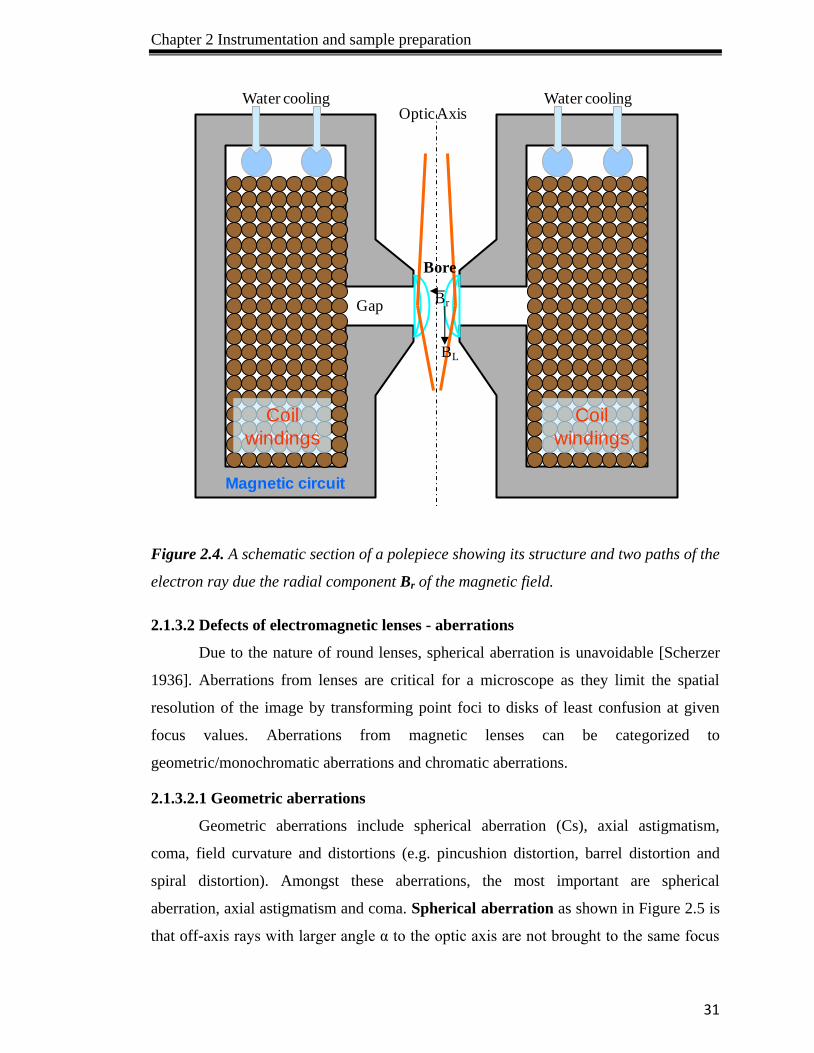
Chapter 2 Instrumentation and sample preparation
31
Figure 2.4. A schematic section of a polepiece showing its structure and two paths of the
electron ray due the radial component Br of the magnetic field.
2.1.3.2 Defects of electromagnetic lenses - aberrations
Due to the nature of round lenses, spherical aberration is unavoidable [Scherzer
1936]. Aberrations from lenses are critical for a microscope as they limit the spatial
resolution of the image by transforming point foci to disks of least confusion at given
focus values. Aberrations from magnetic lenses can be categorized to
geometric/monochromatic aberrations and chromatic aberrations.
2.1.3.2.1 Geometric aberrations
Geometric aberrations include spherical aberration (Cs), axial astigmatism,
coma, field curvature and distortions (e.g. pincushion distortion, barrel distortion and
spiral distortion). Amongst these aberrations, the most important are spherical
aberration, axial astigmatism and coma. Spherical aberration as shown in Figure 2.5 is
that off-axis rays with larger angle α to the optic axis are not brought to the same focus
Gap
Bore
Optic AxisWater cooling Water cooling
BL
Br
Coil
windings
Coil
windings
Magnetic circuit

Chapter 2 Instrumentation and sample preparation
32
point F in the Gaussian image plane as those paraxial rays. Off-axis rays will be
displaced radially from the optic axis as they reach the Gaussian image plane. Therefore,
a point will be imaged by the lens as a blurred disk. The effect of the spherical
aberration can be expressed by the radius of the disk in formula (2.2):
rs ≈ Cs α3 (2.2)
where Cs is known as the coefficient of spherical aberration of the lens. Due to the
physical properties of the magnetic field in round lenses, spherical aberration cannot be
eliminated through careful design of the lens polepieces. However, it can be minimised
by using a strong lens (short focal length) or by using an aperture in the column to limit
the maximum angular deviation α to minimize its effect.
Figure 2.5. A schematic diagram showing spherical aberration - a point object is
imaged as a disk with radius rs≈Csα3 due to spherical aberration that causes the off-axis
rays are not focused at the same point F as those paraxial rays.
Axial astigmatism is caused by one or more of the following reasons: 1)
inhomogeneities in the polepiece material of the lens; 2) geometrical defects in the
manufacture of the ‘cylindrical’ bore of the lens; 3) the build-up of contamination on the
bore of the pole-piece and on the apertures. These potential “defects” will result in a
magnetic field which is no longer axially symmetric. For example, in Figure 2.6, the
magnetic field, Bz, is less powerful in the x-direction than in the normal y-direction. In
this case, electrons originating from a point object on the optic axis may start at equal
angles to the z-axis but those rays travelling in the x-z and y-z planes will be focused at
different points, Fx and Fy, along the z-axis, respectively. Due to astigmatism, points will
be focused by the lens as ellipses with the long axis always normal to the plane within

Chapter 2 Instrumentation and sample preparation
33
which electrons travel rather than disks. The best compromise is achieved at point F, at
which the smallest radius disc is found – the disc of least confusion. Axial astigmatism
can be corrected by a quadrupole lens which is usually referred to as a stigmator. By
using a stigmator, the focal length in the x-z and y-z planes can be made equal thus the
two foci Fx and Fy are brought together to a single point.
Coma is related primarily to rays, which originate from an object point slightly
off the optic axis. All the rays that travel parallel to the optic axis or through the centre
of the lens will still be brought to a point focused on the optic axis but rays which travel
through the peripheral field of the lens with an incident angle will be focused at different
points (see Figure 2.7). This results in an off-axis image which is comet-shaped. Coma
aberration can be avoided by correct alignment of the beam to travel along the optic axis
of the objective lens.
Figure 2.6. Schematic diagram of axial astigmatism [Egerton 2005]. Rays leaving an
axial image point, focused by a lens (with axial astigmatism) into ellipses centred
around Fx if they travel in x-z plane or Fy if they travel in y-z plane, with long axis
normal to the plane they travel, or into a circle of smallest radius - the disc of least
confusion.

Chapter 2 Instrumentation and sample preparation
34
Figure 2.7. Schematic diagram of coma aberration which causes an off-axis object point
imaged as comet shaped. Rays travel through the peripheral field of the lens with an
incident angle are focused at different point from those travel parallel to the optic axis
or through the centre.
Considering the wave nature of electrons, all the geometric aberrations can be
expressed by the wave aberration function, which is defined as the phase difference
between the perfect spherical wavefront and the actual wavefront for a given lens. In
practice, the wave aberration function can be expressed in polynomial form by equation
(2.3) [Hawkes & Kasper 1996, Krivanek 1999], where α is the convergence angle, ϕ is
the azimuthal angle with θx=αcos(ϕ) and θy=αsin(ϕ) and 2π/λ is the incident electron
wavevector:
...])(4/)6(
2/)(4/)(4/)(
3/)3(3/)3(3/)(
3/)(2/)(2/)([2
),(
33
4,3
2224
4,3
22
2,3
44
2,3
222
0,3
22
3,2
22
3,2
22
1,2
22
1,22,1
22
2,1
22
0,1
yxyxbyyxxa
yxyxbyxayx
yxybyxxayxyb
yxxayxbyxayxyx
CC
CCC
CCC
CCCC
(2.3)
In equation 2.3, aberration coefficients are denoted by Cn,m where C denotes an axial
aberration, n is the order of the aberrations and 2π/m denotes the smallest rotational
angle that results in the same phase shift (for m ≥ 1). Note m=0 is used for cylindrically
symmetric aberrations. Moreover, the suffixes a and b refer to 2 mutually orthogonal
contributions to the same aberration that arise for all non-cylindrically symmetric
aberrations. The θx2 + θy
2 term is equal to α
2 and highlights the rotationally symmetric

Chapter 2 Instrumentation and sample preparation
35
nature of the C1, C3 and C5 aberrations. For comparison, table 2.1 shows a list of all of
the aberration coefficients up to, and including, fifth order with corresponding
conventional names. Please note, there are other conventions in use for the definition of
the aberration coefficients in the power series expansion, which were not used in this
work [Hawkes 1989, Uhlemann 1998].
Table 2.1 Aberration coefficients and their corresponding conventional names
Aberration
Coefficients Conventional Name
Azimuthal
symmetry
C01 C01a x Image Shift
1-fold C01b y Image Shift
C10 Defocus Circular
C12 2-fold Astigmatism 2-fold
C21 Coma 1-fold
C23 3-fold Astigmatism 3-fold
C30 (3rd
order) Spherical Aberration Circular
C32 2-fold Astigmatism of Cs
(or 3rd
order 2-fold Astigmatism) 2-fold
C34 4-fold Astigmatism of Cs 4-fold
C41 4th
order Coma 1-fold
C43 4th
order 3-fold Astigmatism 3-fold
C45 5-fold Astigmatism 5-fold
C50 5th
order Spherical Aberration Circular
C52 2-fold Astigmatism of C5 2-fold
C54 4-fold Astigmatism of C5 4-fold
C56 6-fold Astigmatism of C5 6-fold
2.1.3.2.2 Chromatic aberration
Chromatic aberration (see Figure 2.8) arises principally because of the energy
spread in the electrons emitted from the electron source (like light with different
wavelengths), as well as instability of the gun acceleration voltage and lens current
fluctuations. There may also be chromatic aberration effects in the post specimen lenses
for electrons that have experienced inelastic interactions with the sample. Due to
chromatic aberration, electrons with lower energy will be deflected more strongly by the
field, resulting in a higher focusing power and thus a shorter focal length. Consequently,
chromatic aberration results in electrons with a range of energies being focused in

Chapter 2 Instrumentation and sample preparation
36
different planes. For example, electrons emerging from the specimen with no loss of
energy are less strongly focused than those that suffered from energy loss in the
specimen. The effect of chromatic aberration on image resolution will be discussed in
section 2.1.4.2.
Figure 2.8. A schematic diagram showing electrons with different energies being
focused at different planes due to chromatic aberration.
2.1.4 Image resolution and aberration correction
Since the invention of the first electron microscope by Knoll and Ruska in 1932,
the development of electron microscopes has always been driven by efforts to improve
imaging resolution. According to the Rayleigh criterion, which defines the smallest
resolvable distance between two points scatterers, resulting a central drop of the signal
down to 75% of the maximum signal, the theoretical limit for point-to-point image
resolution d can be calculated by formula (2.4) at a given wavelength λ and convergence
semi-angle α (see Figure 2.9),
/22.1dd (2.4)
which is also known as diffraction-limited resolution. Thus, the image resolution can be
improved by increasing the acceleration voltage and/or by reducing the aperture size.
However, there is a knock-on threshold, above which atoms may be displaced from their
lattice sites by inelastic interactions with electrons, which limits the useable acceleration
voltage for any given material. Reducing the aperture size will eventually increases the
diffraction effect, which again will suppress the improvement of resolution [Rose 2005].
Although, in a “perfect” imaging system, the resolution should only be limited by the
diffraction, in reality, spherical aberrations and chromatic aberrations are unavoidable to

Chapter 2 Instrumentation and sample preparation
37
Figure 2.9. A schematic diagram of a focused beam on the specimen in CTEM showing
the definition of convergence semi-angle α, which is determined by the condenser lens
and condenser aperture and collection semi-angle β, which is determined by the
spectrometer entrance aperture.
Figure 2.10. A schematic plot of sinχ(α) versus α showing the contrast transfer as a
function of spatial frequency with uncorrected TEM. The first crossover indicating the
maximum allowable spatial frequency for intuitive image interpretation. Es is the
envelope of spatial coherence of the source and Et is the chromatic aberration envelope.

Chapter 2 Instrumentation and sample preparation
38
rotationally symmetric electromagnetic lenses [Scherzer 1936], which put additional
limits on the image resolution. Achieving optimum performance of a microscope is a
balance between aberrations and diffraction. With simple geometric optics approach
(square root of the sum of the squares of each contributor), this balance could be
achieved by finding an optimum value of convergence semi-angle α. With a more
rigorous wave optical treatment, this balance is essentially guided by the contrast
transfer function (CTF), which is applicable for coherent imaging e.g. HRTEM and BF
STEM imaging, or by the optical transfer function (OTF) which is applicable for
incoherent imaging e.g. HAADF imaging. With coherent imaging, the CTF is defined
by sinχ(α) with χ(α) defined as the aberration function. A plot of sinχ(α) against α in
Figure 2.10 shows the contrast transfer as a function of spatial frequency within the
image [Hall 1953]. It shows maxima whenever the aberration function χ(α) assumes
values of ±2
m (m is an odd number) and zero contrast when χ(α) is ± nπ (n is integral).
Specific frequency components above a certain value can be removed by using an
aperture, and to achieve a simple and interpretable image contrast with all spatial
frequency components having the same sign, the aperture needs to be placed at the first
crossover (first zero contrast point) of CTF at Scherzer defocus. Therefore, the CTF
gives an indication of the maximum allowable frequency to ensure intuitive image
interpretation. In practice, the oscillations of χ(α) in CTF are modified by the spatial
coherence of the source Es and by chromatic aberration effects Et which can be
described by an envelope function. The effect of the envelope function is to impose a
virtual aperture in the back focal plane of the objective lens resulting in damping of
higher spatial frequencies that might normally pass through higher-order windows. This
cut-off imposes an ultimate resolution limit on the microscope, which is called the
“information limit”. In the case of incoherent imaging, as widely used in STEM, the
OTF is defined as the Fourier Transform of the STEM probe intensity function.
Generally it is a positive, monotonically decaying function but with a doubled spatial
frequency range, compared with the CTF for the same lens parameters [Nellist 2011].
This means that the aperture radius can almost be as twice large as that for coherent
imaging, meaning that a higher spatial resolution can be readily achieved for incoherent
imaging.

Chapter 2 Instrumentation and sample preparation
39
2.1.4.1 Spherical aberration limited image resolution
In a STEM, the image resolution is limited by the probe size formed by the pre-
specimen lenses of the microscope. In a simple geometric optic approach, there are three
factors that contribute to the probe size: the effect of a finite source size (the ‘gun’), the
aberrations induced by rotationally symmetric lens (the spherical aberration (Cs or Cn0)
term), and the diffraction limit. Contributions from these factors can be expressed by
formula (2.5):
2
1
2
0
22
22
2/1222 ])()61.0()4
[()( n
nn
probe
sphds CAB
Idddd
(2.5)
where B is the brightness of the source, α is the convergence semi-angle and λ is the
electron wavelength. An is a numerical constant, which for the third order case, A3, is
1/4; as the order of aberration increases it is normally taken as unity. Cn0 is defined as the
spherical aberration coefficient (e.g. for C30). By choosing an appropriate
demagnification of the source to set ds to the required value for a given current Iprobe, the
minimum probe size with an optimum probe angle, αopt, can be obtained. The ultimate
probe size is determined by the optimized value of αopt. For a conventional TEM
without aberration correction in the STEM mode, this value is typically restricted to the
order of 10 mrad due to unavoidable aberrations of the round electron lenses, resulting in
the resolution of about 100 times the electron wavelength. With aberration correction,
this αopt value could be several times bigger. While the geometric approach suits a larger
probe where the source size term dominates, it consistently overestimates the size of the
probe and underestimates the size of the optimum convergence semi-angle for high
resolution STEM imaging. Nevertheless, it can be taken as a guide on how to optimise
performance. A wave-optical treatment can give a more realistic solution by considering
more details with variation of these parameters. According to wave-optical theory and
based on Scherzer aberration function
24
2
1
4
12)(
fCs [Scherzer 1949]
with maximum allowable phase shift of π/2 across the objective lens, if considering the
spherical aberration only up to 3rd
order, then the minimum attainable probe size at given
optimized α is [Scherzer 1949]:

Chapter 2 Instrumentation and sample preparation
40
41
3
303 )(43.0 Cd with 4
1
30
41
30
41.14
CC
(2.6)
which for 100 kV (λ=3.7pm) and C30 = 1.0 mm gives a minimum probe size of 2.0 Å
with αopt about 15.5 mrad and for 200 kV (λ = 2.5 pm) with C30 = 0.5 mm is 1.2 Å. For
the same instrument with C3-corrector (C3 fully corrected), the probe size is limited by
C5 which gives
61
5
505 )(43.0 Cd with 6
1
50
61
50
41.14
CC
(2.7)
For 100 kV and C5 = 100 mm is 0.87Å with αopt about 32mrad and for 200kV and C50 =
5 mm is about 0.38Å. Thus the resolution is improved by a factor of about 2 for 100 kV
STEM. With aberration correction, even the resolution at lower accelerating voltages
(100 kV) can still be better than that at higher accelerating voltages (at 200 kV) without
correction. With spherical aberration correction, there is no need to use very high
acceleration voltage or to make a further reduction of the geometrical pole-piece
dimensions of objective lenses to reduce the spherical aberration for the improvement of
resolution [Haider 1998].
2.1.4.2 Chromatic aberration limited image resolution
Just like spherical aberration, chromatic aberration is another major problem that
needs to be tackled in order to improve the resolution of electron microscope especially
for lower acceleration voltages because chromatic aberration effects increase as the
accelerating voltage decreases. Another benefit of chromatic aberration correction in the
post specimen lenses would be for spectrum imaging, which uses inelastically scattered
electrons to reveal information about chemical composition of the specimen on the sub-
nanometer scale or even atomic scale. Chromatic aberration limited resolution can be
defined as [Zach 2009]:
cc C
E
EBd ***
(2.8)
where B is the numerical values of the order of 1, λ is the electron wavelength, E and ΔE
are the mean energy and energy width of the primary beam, respectively, and Cc is the
chromatic aberration coefficients. Formula (2.8) shows us clearly that resolution could
be improved by:

Chapter 2 Instrumentation and sample preparation
41
increasing the acceleration voltage V which defines λ but not always feasible
because of the beam damage effect
reducing the chromatic aberration coefficient Cc
minimising the energy spread of the electron beam ΔE/E
The use of cold field emission and Schottky electron sources together with the
improved stability of high voltage and lens power supplies would reduce the influence of
chromatic aberration considerably. A monochromator could be used to reduce the
energy-spread ΔE of the incident electron beam to 0.1 eV and an energy filter could also
be helpful to reduce the beam broadening after the beam being scattered by the
specimen. However, chromatic aberration is not as important as spherical aberration
with STEM HAADF imaging at high resolution. This is because, in STEM, chromatic
aberration puts an overall weakening of contrast transfer without actually cutting any
spatial frequencies out. [Nellist 1998, Dellby 2001]. The phase difference due to
chromatic aberration is independent of defocus changes, which are used to compensate
for Cs. Thus, the effects of chromatic aberration become less important and negligible
than spherical aberration. But chromatic aberration correction will still be very useful for
improving the spatial resolution for electron energy loss spectrum analysis and becomes
more important for low voltage STEM.
2.1.4.3 Diagnosis of spherical aberration – the electron Ronchigram
After Scherzer had realised that spherical and chromatic aberrations are
unavoidable for round lenses, he proposed non-rotationally symmetric multipole lenses
[Scherzer 1947] to correct chromatic and spherical aberrations. But his attempts at a
practical realisation of this were unsuccessful due to the extraordinary complexity of
aligning the instrument by hand including the corrector system, together with electrical
instabilities in the power supplies. This use of the electron Ronchigram together with
new computer technology have provided a convenient route for the diagnosis of
spherical aberration, and thus have made aligning a STEM a practical proposition
[Dellby 2001, Krivanek 1999]. The electron Ronchigram is very useful in diagnosis of
spherical aberration and optimum objective aperture size.
Figure 2.11 shows a typical electron Ronchigram simulated by computer with an
amorphous sample in STEM with spherical aberration present. Similar features are

Chapter 2 Instrumentation and sample preparation
42
readily seen experimentally. In the simulation, the specimen was placed at a position
giving a small but finite defocus, in order to see the aberrations of the uncorrected lens
easily. The very centre of this image is a normal shadow image of the specimen at rather
high magnification, known as “sweet spot” as marked by a green circle. The size of the
“sweet spot” can be used as a guidance of the optimum objective aperture size to
exclude rays distorted by spherical aberration and other uncorrected aberrations whilst
maintaining the largest possible probe convergence angle, and thus optimises the probe
size. Within this region, the spatial information of the sample is delivered faithfully with
no distortion due to spherical aberration. Beyond this region, there are two characteristic
rings caused by the spherical aberration from objective lens. The inner one is streaked
out in the radial direction, which is called the ring of infinite radial magnification. The
outer one is a ring formed by high angle rays, where everything is streaked out into a
circular pattern and is called the ring of infinite azimuthal magnification. Other
aberrations might cause the Ronchigram to be not be circularly symmetric, for instance,
astigmatism will cause the rings to be elliptical. Therefore, in order to get a good STEM
image, the Ronchigram must be as round as possible and the details of the Ronchigram
are a powerful and useful guide in optimising lens, stigmator and corrector settings to
minimise aberrations. This adjustment may be done by a skilled operator, or
automatically, by suitable software.
Figure 2.11. A typical electron Ronchigram with two characteristic rings of infinite
magnification appear around the sample shadow image showing spherical aberration.
High angle rays
Axial rays
Radial infinite
magnification
Specimen
Azimuthal ring of infinite
magnification
Shadow image
of specimen
Optic
axis

Chapter 2 Instrumentation and sample preparation
43
2.2 Imaging
2.2.1 Image contrast
For photography, contrast is the difference in visual properties that makes an
object (or its representation in an image) distinguishable from other objects and the
background. Increasing contrast can help to improve the image resolution. With TEM
image, contrast is defined as the variation of electron intensities between neighbouring
regions. The contrast of BF images in CTEM is dominated by diffraction contrast or
phase contrast, depending on the size and location of the objective aperture, and
sometimes with mass-thickness contrast present. Contrast from conventional dark field
(DF) imaging or medium angle annular dark field imaging (MAADF) in STEM is very
similar to that of conventional BF imaging. “Z-contrast” from Rutherford-like scattering
is strongly dependent upon the atomic number and is well-known as the principal source
of contrast in HAADF images. Contrast from HAADF imaging is therefore more mass-
thickness dependent than that from BF, DF and MAADF imaging.
2.2.2 Bright-field and dark-field diffraction contrast imaging –
coherent imaging
A bright-field (BF) image is formed by selecting the direct beam (undiffracted
electrons) travel through the objective aperture with small angle (5~20 mrad) and a dark-
field (DF) image can be formed either by shifting the objective aperture to the selected
Bragg-diffraction spot or (preferably) by tilting the incident beam so that one of the
diffracted beams is on axis to form the image. The method of tilting the illumination has
the advantage that off-axis aberrations are avoided. BF and DF are two common
techniques used for imaging with CTEM. In contrast to high angle angular dark field
(HAADF) imaging with STEM, which is an incoherent imaging technique as will be
discussed in the following section, BF and DF imaging are coherent. Image contrast for
BF and DF images of crystalline materials is dominated by diffraction contrast, at least
for thin specimens (less than 100 – 200 nm). Figure 2.12 schematically shows how to
form BF and DF images. Generally BF imaging is a quick and useful method for
specimen inspection, imaging the size and morphology of nanostructures. But when
imaging defects such as dislocations, phase boundaries, precipitates, stacking faults, and

Chapter 2 Instrumentation and sample preparation
44
Figure 2.12. Ray diagrams showing how to form BF and DF images. A) a BF image
formed from direct beam. B) a DF image formed from a specific diffracted beam by
displacing the objective aperture. C) a DF image formed by tilting the incident beam so
that the scattered beam is on axis. The area selected by the objective aperture is shown
on the viewing screen below each ray diagram. (Adapted from Williams & Carter 1996).
Figure 2.13. A SAD pattern showing [001] orientation and its related DF image
showing the grain boundaries clearly as marked by the light blue line (BiFeO3 co-doped
with 10% Nd, 3% Ti).

Chapter 2 Instrumentation and sample preparation
45
defect clusters, DF imaging can often be more useful though sometimes need to be
combined with BF imaging. In order to interpret either bright or dark field images, they
need to be coupled with crystallographic information from selected-area diffraction
(SAD). To form a SAD pattern, a selected area aperture, which is located below the
specimen in the first image plane (see Figure 2.2), is inserted to define the area to be
investigated, then the condenser lens settings are changed to provide a broad, parallel
electron beam to form the diffraction pattern consisting of sharp diffraction spots. By
choosing specific diffraction spots in a diffraction pattern for use in the formation of
dark field images, specific features in a crystal, or secondary phases with different
crystal structures or orientations associated with those diffraction spots can be defined
and characterised. Within our study, SAD is essential for choosing grains of interest –
which in our case means of specific crystallographic orientations. Figure 2.13 shows a
SAD pattern and its related DF image of the grain we studied indicating the grain
orientation is [001] along the beam direction.
2.2.3 High angle annular dark field (HAADF) imaging with STEM –
incoherent imaging
HAADF images are formed by collecting those electrons (mostly from
Rutherford scattered electrons) scattered to high angle with an ADF detector, as
proposed by Howie (1979) in STEM. Figure 2.14 schematically shows the relative
positions of different detectors, which can be used for imaging. When the inner angle of
the HAADF detector exceeds a critical value, normally over 40 mrads, thermal diffuse
scattering (TDS) resulting from the thermal lattice vibration (approximately equivalent
to Rutherford scattering) will progressively dominate over coherent elastic scattering
from the specimen [Hall 1965] and predominantly falls upon HAADF detector.
Therefore the HAADF image will not be strongly affected by Bragg diffraction effects.
The HAADF image is also referred as a Z-contrast image because of its sensitivity to the
variation of the atomic number, which would be approximately proportional to Z2 for
isolated atoms (Rutherford 1911).
Considering the screening effect of the orbital
electrons, the exponent could be less than 2, depending on the actual value of the inner
and outer angles of the detector [Hartel 1996]. For an uncorrected STEM, operated at
100 kV with a semi-illumination angle α of 10 mrad, an inner angle of 60 mrad will give

Chapter 2 Instrumentation and sample preparation
46
a good contrast. For SuperSTEM2, a 5th
order corrected STEM, with a value of α of
30mrad, it is found that an inner angle of ~100 mrad is suitable and this results in an
outer angle of ~185 mrad for this microscope [Craven 2011].
Figure 2.14. Schematic diagram shows relative positions of different detectors with
semi-angles θ1< 10mrad (BF), 10mrad<θ2<50mrad (MAADF), θ3>50mrad (HAADF).
HAADF imaging has become the most widely used imaging method in STEM.
Images with atomic resolution acquired by HAADF detectors in aberration corrected
STEM are, in general, more straightforward to interpret than HRTEM images due to the
nature of incoherent imaging, which gives no contrast reversals over a wide range of
spatial frequencies, as discussed in section 2.1.4. Contrast reversals may happen with
HRTEM due to the specimen thickness or the objective-lens defocus [Pennycook 1990].
In the HAADF image, bright contrast generally indicates the presence of atoms or atom
columns. However, HAADF imaging alone cannot uniquely identify atoms by just using
the change of contrast in the image, except in some very well-defined cases [Allen 2008,
MAADFHAADF
BF
Specimen
Outer radiusInner radius
Incident beam
HAADF
θ2
θ3
θ1

Chapter 2 Instrumentation and sample preparation
47
Krivanek 2010]. In general, to be able to determine the compositional changes at atomic
scale, a fine focused probe with STEM and an electron energy loss spectrometer and/or
x-ray spectrometer need to be used as a complementary way. In the following section,
we will discuss electron energy-loss spectrometry in more detail.
2.3 Electron Energy-loss Spectroscopy
2.3.1 Interactions of electrons with sample
TEM works via the interaction of a fast electron beam with a thin specimen.
Considering both the particle and wave aspects of the character of electrons, electron
interactions with specimen can be classified as elastic scattering, inelastic scattering,
coherent and incoherent scattering. Figure 2.15 shows some of the important interactions
of fast electron beam with thin specimen. Here we will only outline two main processes:
elastic scattering and inelastic scattering.
Figure 2.15. Schematic diagram showing interactions of a direct beam with specimen.
2.3.1.1 Elastic scattering
Considering electrons as particles, when they interact with an isolated atom,
elastic scattering can happen via one of two ways: either as a result of electrons
interacting with electron cloud and scattered through small angles of a few degrees
(1~2º), or attracted to the positive nucleus and scattered through large angles up to 180°.
Elastic scattering will not cause energy loss for electrons. Within crystalline materials,

Chapter 2 Instrumentation and sample preparation
48
the low-angle elastic scattering is strongly affected by the arrangement of atoms (atomic
planes) within the specimen. Such collective scattering by atoms with the same
arrangement in the crystal is referred as diffraction and can be understood as coherent of
electron waves. Diffraction is mainly controlled by the incident angle of the electron
beam to the atomic planes in the specimen and the spacing of these atomic planes with
which it should satisfy the Bragg condition nλ=2dsinθ (n is an integral). Low-angle,
coherent elastic scattering is invaluable in charactering the crystallography of the
specimen. As the scattering angle becomes larger, the degree of coherency becomes less
due to the introduction of thermal diffuse scattering of the atoms, thus high-angle elastic
scattering, which is also termed as Rutherford scattering, is incoherent. High-angle
incoherent scattering is highly dependent on the atomic number Z of the atoms in crystal
as discussed above in section 2.2.3
2.3.1.2 Inelastic scattering
In contrast to elastic scattering, inelastic scattered electrons of the incident beam
will lose some energy in an interaction with the specimen. Energy-loss of incident
electrons may occur through procedures like generation of characteristic X-rays or
Auger electrons via ionisation of inner-shell electrons, ejection of secondary electrons
from the conduction or valence bands of the atoms in the specimen, excitation of
plasmons and phonons, and even the damage to the specimen through a number of
mechanisms. The two important characteristics of inelastic scattering are the energy loss
E and the scattering semi-angle, which determines the efficient collection angle of the
spectrometer. Analytical electron microscopy can be performed using an electron
energy-loss spectrometer. An EEL spectrum recorded by a spectrometer can contain
abundant information about the elemental composition and chemical bonding of the
specimen, as well as other features including the electronic structure of the specimen.
2.3.2 Electron energy-loss spectrometer
SuperSTEM2 is equipped with a Gatan Enfina electron spectrometer to record
EELS in parallel and its main part is a sector magnet. A sector magnet typically consists
of a homogeneous magnetic field normal to the electron beam. Usually for mechanical
convenience the electrons are bent through a 90° angle and the Lorentz force causes
electrons of different energy to emerge from the spectrometer at different angles. The

Chapter 2 Instrumentation and sample preparation
49
spectrometer magnetic field is provided by two parallel polepieces with two current
carrying coils providing the excitation. In practice, the polepieces and coils are at
atmosphere pressure. An evacuated drift or flight tube, connected to the microscope
vacuum system, passes between the two polepieces. An offset voltage may be applied to
this drift tube to alter the kinetic energy of all the electrons and rigidly shift the whole
energy loss spectrum across the detector system. In order to record the intensity at each
particular energy loss as sequence of digital values over a large number of detector
channels, a multi-element detector is normally employed to record the whole spectrum
in parallel. A spectrometer with this kind of detector is called a parallel-recording
spectrometer. The energy resolution of the resulting EELS is mainly determined by the
energy spread of the electron source, the resolution of the spectrometer itself, and the
resolution of the detection system though there are other factors. Spectrometer
dispersion is the vertical displacement of the electron beam per unit change in electron
energy and it is typically a few micrometres per eV at the exit of the magnet. There are
multipole lenses after the magnet sector to allow the dispersion to be varied for a
specific energy range of the spectrum to be recorded. In general, the angular acceptance
angle of a spectrometer is much smaller than the angular range that needs to be
collected, especially with aberration corrected microscopes such as SuperSTEM2. The
significantly enlarged probe convergence semi-angle in such microscopes has increased
the difficulty of EELS signal collection. This is because a large portion of the available
signal will be lost if the collection angle is not big enough, therefore, it is important to
collect over at least the same angular range as the probe for relatively low energy losses
and over an even larger range for higher losses. With SuperSTEM2, the QOCM is
specially designed for coupling the inelastically scatted electrons into the small entrance
aperture of the spectrometer, and can also be used to correct for the higher order
aberrations of Enfina spectrometer. Because QOCM does not influence the imaging
process except for allowing the collection angles of detectors to be varied/coupling the
spectrometer to the microscope, and the 4 projector lenses are only excited for forming
diffraction patterns and CTEM images, thus there is no imaging lens after the specimen
for EEL spectra and the specimen is directly in the object plane of the spectrometer;
therefore the area irradiated by the probe becomes the spectrometer object and its size is

Chapter 2 Instrumentation and sample preparation
50
determined by the size of the electron probe, which is about 0.7Å and has effectively
improved the spatial resolution for analysis.
2.3.3 EELS
After interactions with the specimen, electrons will undergo either elastic
scattering or inelastic scattering. A spectrum recorded by a spectrometer will contain
peaks produced by electrons with and without energy loss. Basically, a typical spectrum
can be recorded with three different regions – the zero-loss peak, the low-loss region and
the core-loss region, as shown in Figure 2.16. Depending on the information required,
specific energy ranges can be selected for a spectrum.
Zero-loss peak: The zero-loss peak (ZLP) primarily contains electrons that are
elastically forward-scattered and also electrons that have suffered minor energy loss not
resolvable by the spectrometer. Normally, the FWHM (full width at half maximum) of
the zero-loss peak can be used as an indicator of the total resolution of a
spectrometer/microscope system.
Figure 2.16. EELS showing different energy loss regions of spectrum. A) a spectrum
showing ZLP marked in orange rectangle and the rest of the peaks are plasmons caused
by multiple excitation; Plasmon peaks are rather high because the sample is very thick.
B) a spectrum showing core-loss region with characteristic ionization edges labelled.
Low-loss region: In this region (e.g. < 50 eV), energy losses are mainly due to
interactions with oscillations of weakly-bound (outer-shell) electrons ("plasmons") in the
specimen, as well as interband and intraband transitions. Intensity in this region of the
spectrum can, for instance, give information on sample optical properties. Specimen
thickness, relative to the inelastic scattering mean-free path, can also be easily
determined by the ratio of the intensity of the whole spectrum to the intensity of the
Fe L3, L2 O K
ZLP
Plasmon peaks Nd M
Ti L3, L2
A B

Chapter 2 Instrumentation and sample preparation
51
zero-loss peak. With high-resolution EELS, we might be able to measure the energy
bandgap for some materials. But to achieve this, a very narrow energy spread beam is
needed in the microscope, probably created using a monochromator.
Core-loss region: Energy loss in this region (extends from about 40 or 50eV to
several thousand eV) is caused by inelastic excitation of inner-shell electrons to
unoccupied states above the Fermi level. This region therefore reflects the atomic
character of the specimen. An abrupt increase in intensity in the spectrum at an energy
loss equal to an inner-shell ionisation energy is termed an ionization edge. Since the
energy of the edge threshold is determined by the binding energy of the particular
electron sub-shell within an atom, the ionisation edge energy is characteristic of a
particular chemical element and is known for every electron shell, thus ionisation edges
can indicate which elements are present within the specimen. Choosing a window of an
energy loss (around 10eV or more in width) corresponding to an inner-shell ionization
edge of a known element, an elemental map that represents the distribution of that
element can be formed, possibly with spatial resolution down to atomic resolution
depending on the set up of the microscope. This compositional mapping technique is
probably the most powerful use of inelastic scattering. Above the edge onset, within the
first 30-40eV, is defined as electron energy loss near-edge structure (ELNES). ELNES
can give a direct insight of the associated electronic structure and atomic bonding in the
solid, like determination of local coordination by using “coordination fingerprint” or
valence states of atomic species. This is because, in solids, the unoccupied electronic
states just above the Fermi level can be significantly modified by the chemical bonding
between neighbouring atoms leading to a complex but specific density of states (DOS)
which will be reflected by the ELNES as spectral fingerprint. By using a proper
collection aperture to satisfy the dipole selection rule (Δ = ±1), different edges of the
same element can represent different symmetries of the final state, for instance, a K-edge
will probe the unoccupied p-like DOS, while an L2,3-edge will probe the unoccupied s-
and d-like DOS. Beyond the near-edge region, a region of weaker, extended oscillations
is superimposed on the gradually decreasing tail of the core loss edge. This region is
known as extended energy loss fine structure (EXELFS). The details of the oscillations
may be used to probe the coordination of a particular atom.

Chapter 2 Instrumentation and sample preparation
52
2.3.4 Spectrum imaging
Spectrum imaging (SI) is a technique which is deployed to acquire an energy-
loss spectrum at each pixel as the STEM probe is rastered over the specimen. With
spectrum-imaging technique, a four-dimensional data array is created which corresponds
to electron intensity within a three-dimensional volume of (x,y,E) space [Jeanguillaume
and Colliex 1989], Figure 2.17. As the probe is scanned by the computer and spectra are
acquired by the computer, this concept has now been extended to record a wide range of
data at each pixel simultaneously, like electron dispersive x-ray, HAADF and EEL SI.
However, as STEM acquisition is point by point and EEL spectrum imaging takes a
significant time, drift caused distortion of the image is unavoidable. To minimise this,
drift correction is very important. This is achieved by recording a drift correction area
with a short exposure survey then re-require it after every tenth line of the spectrum
image acquisition. By comparing the re-required images to the original, the magnitude
and direction of the drift can be determined and corrected. To make the recording times
realistic, a parallel-recording spectrometer like the Gatan Enfina, which means many
spectra can be stored on the chip before reading out, is needed. Besides, incorporating
drift correction to limit the distortion of the image and the simultaneously acquired
image to ensure perfect registration between the spectral data and position is also
necessary. For EEL spectrum data analysis, ideally, both the low loss and the core loss
regions of the EEL spectrum should be recorded under the same electron optical
conditions at the same pixel before moving to the next pixel to ensure perfect
registration. However, the large dynamic range of the EEL signal means that a single
integration time cannot be used to record the whole spectrum. To overcome this limit
and also to reduce the sample damage caused by the incident beam, a fast beam switch
(FBS) [Craven 2002, Scott 2008] is very useful. The FBS has a sub-microsecond
response time which allows rapid shuttering of the beam and so is capable of handling
the large range of exposure times required to cover both core and low loss spectra. As a
consequence, a core loss spectrum at each pixel can be collected after a low loss
spectrum with the same electron optical conditions. As the datasets have “exact” pixel
correlation, it is possible to correctly remove multiple scattering from the EELS core
edges, either by Fourier-ratio deconvolution or by splicing the EELS SIs together and
using Fourier-Log deconvolution. The spectra can also be normalized for intensity

Chapter 2 Instrumentation and sample preparation
53
allowing absolute quantification [Craven 2008]. This technique is also known as dual
EEL spectroscopy. Unfortunately, the present set up of SuperSTEM2 does not have a
FBS, thus it is not possible to do the absolute quantification with the defects as will be
discussed in chapter 4 and chapter 5. But the complete dataset still can be processed for
quantitative analysis like elemental mapping to show the two-dimensional distribution of
a chosen element or a specific chemical bonding using ELNES signatures. With
aberration correction, SuperSTEM2 has achieved probe sizes down to sub-Angstrom
dimensions. Such a fine probe, combining simultaneous HAADF imaging with Gatan
Enfina spectrometer, has enabled the generation of elemental maps with atomic
resolution, as will be shown in chapters 4 and chapter 5. Such high spatial resolution is
difficult for energy filtered imaging in the CTEM (EFTEM), which involves the
selection of an energy losses window from the transmitted electron beam via use of
energy selecting slit after the EEL spectrometer, to achieve without a chromatic
aberration correction. EFTEM is more suitable for mapping unknown elemental
distributions from larger fields of view with relatively short acquisition times while
STEM is excellent with regions need more detailed analysis because it allows the
maximum information per incident electron to be acquired with good spatial registration
as well as the orchestration of the acquisition [ Crave 2011].
Figure 2.17. A schematic diagram of spectrum imaging technique, which can be used
for quantitative analysis [Jeanguillaume and Colliex 1989].

Chapter 2 Instrumentation and sample preparation
54
2.4 Sample Preparation
2.4.1 Ceramic preparation
Co-doped BFO ceramics were prepared by our collaborators at the University of
Sheffield. The preparation procedure is conventional mixed oxide synthesis [Kalantari
2011], using Bi2O3 (99.9 %, Acros Organics), Fe2O3 (99.8 %, Alfa Aesar), TiO2 (99.99
%, Sigma Aldrich) and Nd2O3 (99.90 %, Sigma Aldrich) as the starting reagents. The
appropriate amounts of dry raw materials were weighed and attrition milled for an hour
with yttria-stabilised zirconia media in iso-propanol. Mixed powders were calcined for 3
h at the optimum reaction temperature which is 1020°C for (Bi0.85Nd0.15)(Fe0.9Ti0.1)O3.
The reacted powder was sieved through a 355 μm sieve and then attrition milled as
above. The powder was pressed into pellets of 10 mm diameter and ~ 2.5 mm thickness
by uniaxial pressing at an applied load of 1 ton for 1 minute. Pellets were then sintered
in air for 3 h at an optimum sintering temperature, which is 1050°C. The optimum
sintering temperature was judged to be that at which the proportion of secondary phases
was minimal and density > 95 % of the theoretical density.
2.4.2 Specimens for TEM
All the specimens used for the TEM/STEM experiments in this thesis are planar
samples, which were prepared by a conventional procedure of cutting, mechanical
thinning, dimpling, and ion beam milling.
Cutting and pre-thinning disks: 3mm - diameter disks are made from the
10mm pellet by using the Ultrasonic Disc Cutter, then the disks are pre-thinned to about
80 - 100 micrometers by hand-grinding.
Dimpling: Disks pre-thinned in previous step are then put in a Gatan dimple
grinder to thin the centre of the disk to a thickness of about 20 μm. The dimpler uses a
rotating brass wheel coated with diamond paste to grind material from the surface of the
disk. A specific rotational speed and weight can be applied to the wheel to accurately
thin the disk on both sides. A higher grade diamond paste is also used with a soft felt
wheel for a final polish. To remove the debris from grinding, manually rinsing is
necessary.
Ion milling: The pre-thinned sample is then put in a Gatan Precision Ion
Polishing System (PIPS), model 691, modified with a low voltage supply and cold stage

Chapter 2 Instrumentation and sample preparation
55
for ion milling in order to get the specimen thickness to electron transparency. The PIPS
uses two argon ion guns that can be directed with specific angles of incidence onto the
sample surface. Using a small angle of incidence (from surface) is preferable for two
reasons. First, ion implantation is greatly reduced at glancing angle; furthermore, any
preferential thinning of different materials is minimised [Williams & Carter 1996]. The
ion guns were orientated at ±4° incident angles which allow both side of the sample to
be milled simultaneously. Within our study, samples were initially milled at an
acceleration voltage of 4 kV while being rotated at 2 rpm for approximately 4 hours,
then the acceleration voltage was reduced to 1 kV for about 2-3 hours and 500 V for
about 30 minutes until light was visible through a small hole formed at or near the centre
of the sample. The reason for reducing the acceleration voltage is to minimise surface
damage introduced by ion bombardment.
Figure 2.18. Images of same silicon sample taken at same conditions of TEM. a) Before
gentle milling. b) After gentle milling.
Ion Polishing: final ion polish was, in some case, performed using a
TECHNOORG LINDA Gentle Mill, Model IV5. This low kV ion mill was operated at
300eV with an ion incidence angle of 12 degrees. Each side of the sample was milled for
15 minutes. This final polishing procedure improves the surface quality of the prepared
sample by minimising any amorphous layer produced by earlier stages of preparation.
Figure 2.18 shows two TEM images of a silicon sample before and after gentle milling,
respectively. It is very obvious that the surface of the sample is rather rough after initial
a b

Chapter 2 Instrumentation and sample preparation
56
milling, as shown by the patches of different intensities across the image, as compared
with the image taken after the gentle mill.
Carbon Coating: After the final stage of ion polishing, finally the TEM samples
were carbon coated on both sides using thermal evaporation of carbon to prevent
charging from the electron beam. Otherwise, a number of undesired effects can occur
during investigation with TEM/STEM including unpredictable sample movement, focal
or astigmatism drift, and even sample breakage.
References:
Allen J. E., Hemesath E. R., Perea D. E., Lensch-Falk J. L., Li Z.Y., Yin F., Gass M. H.,
Wang P., Bleloch A. L., Palmer R. E., Lauhon L. J., (2008) High-resolution
detection of Au catalyst atoms in Si nanowires, Nature Nanotechnology 3(11),
676-681.
Craven A. J., Wilson J. and Nicholson W.A.P., (2002) Ultramicroscopy 92, 165-180.
Craven A. J., MacKenzie M. and McFadzean S., (2008) Dual energy range EELS
spectrum imaging using a fast beam switch, EMC2008: Vol 1, Instrumentation
and Methods / edited by Luysberg M. et al., Springer ISBN 978-3-540-85154-7,
363-364.
Craven A. J., (2011) in Aberration-corrected analytical transmission electron
microscopy / edited by Brydson R. et al., (Chap. 6), John Willey & sons, Ltd.
Delby N., Krivanek O. L., Nellist P. D., Batson P. E., Lupini A.R., (2001) Progress in
aberration-corrected scanning transmission electron microscopy, Journal of
Electron Microscopy 50 (3), 177-185.
Egerton R. F., (2005) Physical principles of electron microscopy: an introduction to
TEM, SEM, and AEM, New York: Springer Science+Business Media.
Haider M., Rose H., Uhlemann S., Schwan E., Kabius B., Urban K., (1998) A spherical-
aberration-corrected 200 kV transmission electron microscope, Ultramicroscopy
75, 53-60.

Chapter 2 Instrumentation and sample preparation
57
Hall, C. R. and Hirsch, P. B., (1965) Effects of thermal diffuse scattering on propagation
of high energy electrons through crystals, Proceedings of the Royal Society of
London Series A, 286, 158-177.
Hall C. E., (1953) Introduction to Electron Microscopy. McGraw Hill, New York.
Hartel P., Rose H., Dinges C., (1996) Conditions and reasons for incoherent imaging in
STEM, Ultramicroscopy 63, 93-114.
Hawkes P. W., and Kasper E., (1989) Principle of electron optics, Academic Press,
London.
Hawkes P. W., and Kasper E., (1996), Principles of Electron Optics 2, Academic Press,
London and San Diego, Ch. 41.
Howie A., (1979) Image contrast and localized signal selection techniques, Journal of
Microscopy, 117, 11-23.
Jeanguillaume C. and Colliex C., (1989) Spectrum-image: The next step in EELS digital
acquisition and processing, Ultramicroscopy 28, 252-257.
Krivanek O. L., Dellby N., Lupini A. R., (1999) Towards Sub-Angstrom Electron
Beams, Ultramicroscopy 78, 1-11.
Krivanek O. L., Corbin G. J., Dellby N., Elston B. F., Keyse R. J., Murfitt M. F., Own
C. S., Szilagyi Z.S., Woodruff J.W., (2008) An electron microscope for the
aberration-corrected era, Ultramicroscopy 108, 179–195.
Krivanek O. L., Chisholm M. F., Nicolosi V., Pennycook T. J., Corbin G. J., Dellby N.,
Murfitt M. F.,. Own C. S., Szilagyi Z. S., Oxley M. P., Pantelides S. T. and
Pennycook S. J., (2010) Atom-by-atom structural and chemical analysis by
annular dark-field electron microscopy, Nature 464, 571-574.
Kalantari K., Sterianou I., Karimi S.,. Ferrarelli M. C, Miao S., Sinclair D. C., and
Reaney I. M., (2011) Ti-Doping to Reduce Conductivity in Bi0.85Nd0.15FeO3
Ceramics, Adv. Func. Mater., 21, 3737–3743.
Nellist P. D. and Pennycook S. J., (1998) Sub-Ångström resolution by underfocused
incoherent transmission electron microscopy, Phys. Rev. Lett., 81, 4156-4159.
Nellist P. D., (2011) Aberration-corrected analytical transmission electron microscopy/
edited by Brydson R. et al., (Chap. 5), John Willey & sons, Ltd.
Pennycook S. J. and Jesson D. E., (1990) High-resolution incoherent imaging of
crystals, Phys. Rev. Lett., 64, 938-941.

Chapter 2 Instrumentation and sample preparation
58
Rose H. and Wan W., (2005), Aberration correction in electron microscopy, Proceedings
of 2005 Particle accelerator conference, Knoxville, Tennessee, 44-48.
Rutherford E., (1911) The Scattering of α and β Particles by Matter and the Structure of
the Atom, Philosophical Magazine. Series 6, 21, 669-688.
Scherzer O., (1936) Über einige Fehler von Elektronenlinsen, Zeitschrift Physik, 101,
593.
Scherzer O., (1947) Sphärische und chromatische Korrektur von Elektronenlinsen, Optik
2, 114-132.
Scherzer O., (1949) The Theoretical Resolution Limit of the Electron Microscope, J.
Appl. Phys., 20, 20-29.
Scott J., Thomas P. J., MacKenzie M., McFadzean S., Wilbrink J., Craven A. J. and
Nicholson W. A. P., (2008) Ultramicroscopy 108(12), 1586-1594.
Uhlemann S., and Haider M., (1998) Residual wave aberrations in the first spherical
aberration corrected transmission electron microscope, Ultramicroscopy 72, 109.
Williams D. B., Carter C. B., (1996) Transmission electron microscopy, Springer
Science +Business Media, LLC.
Zach J., 2009 Chromatic correction: a revolution in electron microscopy?, Phil. Trans.
R. Soc., A, 367, 3699-3707.

Chapter 3 Computational software related to data analysis
59
Chapter 3 Computational software related to data
analysis
3.1 Introduction
In order to be able to perform quantitative analysis of atom resolution data,
several computational methods have been used for noise reduction, drift correction and
quantitative atomic position measurement. Principal Component Analysis (PCA)
[Jolliffe 2002] is used prior to elemental mapping with EELS to reduce the background
noise and thus improve the visibility weak signals obscured by the background noise.
The Statistically Determined Spatial Drift (SDSD) software [Schffer 2004] is used for
the drift correction and alignment of an image series to produce a high signal to noise
image, which is minimally affected by sample drift. The iMtools package is used for
accurate atom position determination from high-resolution STEM images prior to further
scanning distortion correction. Final scanning distortion correction and averaging of
images of identical features is done using our own routines within Microsoft Excel, as
well as the construction of three dimensional atomic structure models. These models are
then tested in image simulations using the QSTEM package [Koch 2002], which are
used to help interpret the high-resolution images and/or verify the proposed models of
new structures. In some cases, density functional theory calculations were carried out on
our three dimensional structures by external collaborators at the ETH Zürich using the
VASP programme. In this chapter, I will give some brief descriptions of the methods
and background of the computational methods used in the data analysis.
3.2 Principal Component Analysis (PCA)
PCA is one of the most popular forms of Multivariate Statistical Analysis, which
is a useful family of techniques to analyse large datasets containing many known and/or
unknown variables. The general concept of PCA is to identify any statistically
significant features in large data sets and to reduce random noise components efficiently
in a statistical manner [Jolliffe 2002]. This technique is applied to the EEL-SI analysis in
this work by a PCA plug-in for Gatan Digital Micrograph, developed by Masashi
Watanabe [Watanabe 2005], to reduce the random background noise in the spectrum
and thus enhance the weak signals hidden by the noise prior the elemental mapping. For

Chapter 3 Computational software related to data analysis
60
example, in Figure 3.1, the Nd M4,5 signal in the raw EEL-SI is very weak and almost
hidden by the random back ground noise. After the PCA is applied, the weak Nd signal
is enhanced greatly due to the random background noise has been removed. The main
concept of this method is summarised in the following paragraph.
Figure 3.1. Comparison of spectra before and after PCA: left is the raw spectrum; right
is the spectrum after PCA was applied.
With an EEL-SI that contains three-dimensional information, it can be
decomposed into two spatial axes (x,y) and one energy axis (E). By applying PCA, The
EEL-SI dataset can be described by a data matrix formed by the product of a
score matrix , which contains the spatial information (x,y) and is stored in the
columns of the data matrix, and a loading matrix , which includes the spectral
information (E) and is put in the rows [Malinowski 2002],
(3.1)
where the superscript T of represents a matrix transpose; n is the number of principal
components. In the loading matrix , each row is uncorrelated to the other rows and is
called an eigenspectrum of the dataset. The corresponding column of the score matrix
represents the spatial amplitude of each eigenspectrum. Thus, the individual product of
each row of the loading matrix and the corresponding column of the score matrixes
produces a principle component. The number of principal components, n, is
mathematically equal to the smaller number of x*y or E. In the decomposed matrixes,
the principal components are ordered from high to low according to their eigenvalues, so
is the variance or information that they describe.
E)y),((x,D
n)y),((x ,S
T
n)(E,n)y),((x,E)y),((x, L S D
L
TL
S
Nd Nd

Chapter 3 Computational software related to data analysis
61
Figure 3.2. An example of the screen plot, showing the correlation between log
eigenvalue and components. Significant features are represented by those exponentially
decreased principal component, experimental random noise are represented by the
straight line in the scree plot. 10 components reconstructed spectrum image showing the
random back ground noise has been greatly reduced.
Typically, the number of dominant features in the dataset is much less than n,
and many of the weak principal components will therefore describe experimental noise.
If the number of non-noise principal components, m, is determined, the original dataset
can be reconstructed using this limited number of principal components, m:
T
m)(E,m)y),((x,E)y),((x, L S D
m << n (3.2)
As a result of the reconstruction, the experimental noise can be removed efficiently from
the original dataset without losing spatial or energy resolution [Jolliffe 2002, Burke
2006, Bosman 2006, Watanabe 2007]. To determine the value for m, an approach named
as the “scree plot” is used whereby the logarithms of the eigenvalues are plotted versus
the component number (Figure 3.2). Since the eigenvalues of random-noise-containing
principal components decrease exponentially, components that only describe
experimental noise should lie on a straight line in the scree plot. In this work, this
number m was generally in the range of 10 ~ 20. Reconstructed spectrum images using
different number of components have been compared. There are no subtle features have

Chapter 3 Computational software related to data analysis
62
Figure 3.3. Selected pairs of the loading spectra and the corresponding score images of
the components showing significant features are represented by those exponentially
decreased principal components in the scree plot of Figure 3.2.

Chapter 3 Computational software related to data analysis
63
been missed out as long as the number of components for reconstructing is beyond the
number of the breaking point in the scree plot. The only difference between them is that
reconstructed spectrum images with larger number of components have more
background noise induced. Figure 3.2 shows a scree plot and its correlated raw spectrum
image acquired from one of the defects, which will be discussed in chapter 4, and the
corresponding reconstructed spectrum image using 10 principal components indicated
by the scree plot. As a result, the reconstructed spectrum image shows that the random
background noise has been effectively removed from the raw data by PCA. Figure 3.3
gives a further insight on some selected pairs of the loading spectra and their
corresponding score images of the components of the raw EEL-SI and how the number
of principal components provided by the scree plot for reconstructing the EEL-SI is
valid. The loading spectrum of #1 component represents the average spectrum of the
EEL-SI, which means it is always the most significant component in the dataset. Any
component that contains signals higher than #1 indicates its significant difference from
the average. Thus, the loading spectra after #1 component contain positive and negative
peaks. The #4 loading spectrum is dominated by positive O K-edge together with a little
bit of Ti L-edge; C K-edge and Nd M-edge are negative. The corresponding score image
indicates that the dominating O are distributed relatively even within the EEL-SI. The #5
loading spectrum has positive peaks of C K-edge, Ti L-edge and Fe L-edge but with Fe
L-edge signal stronger, Nd M-edge shows a strong negative value, thus the bright
regions in the score image likely represents the distribution of Fe, and the dark contrast
possibly means the distribution of Nd. The #7 loading spectrum contains positive peaks
of C K-edge, Ti L-edge and O K-edge, but with Ti signal competitive to C signal; thus
these relatively brighter 3 spots represent the Ti distribution there. The #8 loading
spectrum has positive C K, Fe L and Nd M peaks, and a negative Ti L peak. However,
as Nd M peak is still relatively weak compared to the C K peak, it is difficult to
discriminate any significant feature of Nd in the corresponding score image. From the
#10 loading spectrum and its related score image, it is obvious that their corresponding
principal can be clarified to the noise component. Over all, by combining the
information from the decomposed components together with the scree plot, the number
of principle components for reconstructing the EEL-SI can be determined reliably.

Chapter 3 Computational software related to data analysis
64
Therefore, PCA can reduce the random background noise effectively and give the
enhanced features of the EEL-SI.
3.3 Drift Correction via the Statistically Determined Spatial
Drift (SDSD) Method
Image processing to extract valuable positional atomic-column data from
HAADF - STEM images is very important for the quantitative analysis. In order to get
the precise location of an atom column with sub-pixel accuracy, corrections for
distortions due to specimen drift or scanning electronic artefacts like hysteresis effects
during the “fly back” between scan lines is necessary [Sanchez 2006]. Since STEM
records the pixels sequentially, and to record a full size image with good signal to noise
ratio always takes a longer exposure, drift is unavoidable.
Figure 3.4. (a) One slice from a series of images taken using a dwell time of 5μs/pixel;
(b) A sum of the image series after spatial drift correction.
To minimize these drawbacks, a stack of the HAADF images with very short
exposure time was taken, and then the SDSD software tool [Schaffer 2004] was used,
which is a plug-in to the Digital Micrograph (DM) software, to carry out the correction
for the sample drift. Finally, a sum of the corrected images was created to increase the
signal to noise ratio (SNR) for the extraction of atom columns’ positions with high
accuracy. Within this work, corrections for distortions were carried out using the FFTW
routines from Christoph Koch [http://www.christophtkoch.com/stem/], and the most

Chapter 3 Computational software related to data analysis
65
reliable cross-correlations were generally achieved using the “Phase Correlation” option
in the SDSD software without any filter being chosen. By cross-correlating all image
pairs with each other and statistically evaluating all the obtained shift vectors, the
algorithm increases its robustness. Outliers can thus be identified and excluded resulting
in a much more accurate drift determination with sub-pixel precision [Schaffer 2004].
Figure 3.4 shows one slice of the image from a stack and the sum of the stack images
after correction. As a result the SNR is improved significantly.
Figure 3.5. Interface of iMtools and fitted peak image (top-right) from the SDSD
corrected HAADF image (left) together with corresponding coordinates list.
Figure 3.6. A chart of the corresponding defect in Figure 3.5 plotted with Excel using
the coordinations (x, y) extracted by iMtools.

Chapter 3 Computational software related to data analysis
66
3.4 iMtools
iMtools programmed by Dr Lothar Houben in Ernst Ruska-Centre Jülich is a
binary software collection and graphical user interface developed for digital image
processing of electron micrographs [http://www.er-c.org/centre/software]. One of its
implementations is the determination of atom column positions from atomic resolution
electron microscope images by two-dimensional (2D) Gaussian fitting to the peak phase
maxima (see Figure 3.5), which allows peak centre interpolation with sub-pixel accuracy
[Houben 2006]. In this thesis, 2D Gaussian peak fitting by iMtools was applied to the
summed HAADF images created by SDSD for the determination of the atom positions
to ensure the precise location of atom columns. Once the atom column positions were
determined, their coordinates were exported to a spreadsheet for the further correction of
the distortions likely caused by imperfections in the scanning system (Figure 3.6).
3.5 Distortion Corrections and Primary Model Development
Figure 3.6 is plotted from the data imported from iMtools showing the atom
column positions of a nanorod with its surrounding doped - BFO matrix along [001]o
direction (here the subscript defines orthorhombic, unless stated otherwise, for example,
to define primitive perovskite structure). The cell parameters of a closely related
composition with the same crystal structure, Bi0.85Nd0.15FeO3, were Rietveld-refined
from x - ray diffraction and neutron powder diffraction data as part of previous works
[Karami 2009, Levin 2010]. Results from these refinements showing that the structure
is of PbZrO3 - type orthorhombic, with cell parameters of a = 5.5959 Å, b = 11.2399 Å,
c = 7.8076 Å. According to the PbZrO3-type orthorhombic structure that has unit cell of
( is the cell parameter of the primitive perovskite) and reducing
this orthorhombic cell to a pseudotetragonal cell, cell parameters of a ≈ b ≈ 3.965 Å, c =
3.904 Å can be obtained. In this case, the cells in the [001]pc direction can be assumed
to be square on average and oriented with a side of 3.965 Å. However, due to the linear
distortions likely originates from small non-idealities in the scanning system, the atom
column positions in the perovskite matrix surrounding the nanorods displayed in
Figure3.6 are clearly not showing squared unit cells. Therefore, to build an atomic
structure model, corrections of these distortions are necessary. The typical procedure of
linear distortion correction includes shifting the origin for the interpolated peak positions

Chapter 3 Computational software related to data analysis
67
to zero, horizontal correction, shear correction and magnification correction to make the
crystal cells in the [001] direction to be square. All the measurement of these corrections
was performed using patches of perfect perovskite structure that are a bit further away
from the defects or anti-phase boundaries by performing least squares fitting to
determine the gradients and spacings of rows of peak positions, and then converting the
fit parameters to correction matrices to apply to the dataset (i.e. rotation, shear, and
magnification and anisotropic expansion matrices). The matrix used for the rotation
correction was constructed from the averaged rotational gradient from the rows of peaks
of those chosen patches of perfect perovskite structure. The matrix for shear correction
was constructed from the averaged gradient of the columns of peaks that should be
vertical to the rows of peaks used for the rotation correction. In general, for shear
corrections, the averaged gradient of the columns of peaks would result in the angle
value of 1.50 radians (about 86 degrees with respect to horizontal axis).
After all the procedure for correction was done, atom positions with identical
features were overlaid and averaged in order to get the unbiased atom positions. Errors
were generally less than 25pm. Then, by correlating the atoms position with the
chemical information from the atomic resolution EELS-SI, proposed structure model
were built up for further test with image simulation or electronic structure calculation.
3.6 Image Simulation
Image simulation is an essential tool in the effective interpretation of high
resolution electron microscope images and is particularly necessary in the study of
crystalline samples where dynamical effects can be important [Kirkland 1987]. This is
because artefacts due to the aberrations of the instrument and/or specimen manipulation
(like thickness and tilt) will be present in the images. Additionally, the beam-specimen
interaction can also have big and complex effects on the images, especially in HRTEM.
Image simulation is therefore essential in the detection and understanding of these
artefacts. Of special interest to this work, in the process of discovering new structures,
proposed models can be verified by comparing calculated images with the experimental
images. Here I will briefly explain a well-known method – the multislice method using
the frozen phonon method for HAADF-STEM image simulation of thick specimens
(>10Å), which was used for the simulations in this study.

Chapter 3 Computational software related to data analysis
68
3.6.1 Multislice algorithm
The multislice algorithm is based on the physical optics theory of Cowley and
Moodie [Cowley and Moodie 1957] and a numerical integration method to solve the
Schrödinger equation. This allows the dynamical simulation of images of thick
specimens. With this method, a thick specimen is divided into thin two-dimensional
slices perpendicular to the electron beam direction (like a loaf of sliced bread) when the
effect of dynamical scattering (whereby the electron is scattered more than once as it
passes through the specimen) is considered. Each slice is thin enough to be treated as a
weak phase object (which only gives a small change in the wavelength of the electrons
as they pass through the specimen) and the propagation between slices is determined
using Fresnel diffraction (waves are treated as spherical waves, not plane waves) over a
distance Δz. In STEM, the wave function ψp( ) of the electron probe incident upon the
specimen at position is given by integrating the aberration wave function
over the objective aperture as
(3.3)
where λkmax=αmax is the maximum angle in the objective aperture and A is a
normalization constant chosen to yield:
(3.4)
As the electron probe passes through each slice of the specimen it is modulated by the
specimen transmission function which is considered as a small, position dependent
phase shift to the wave function due to the slice, which is so thin that it is treated as a
weak phase object. The resulting transmitted wave function is
(3.5)
in which with the total projected atomic potential of the
single specimen slice along the optic axis, which could be calculated from the electron
x
)](exp[ ki
kdxxkikiAxx p
k
pp
2
0)](2)(exp[),(
max
1),( 22
xdxx pp
)(xt
),()](exp[),()(),( ppzpppt xxxixxxtxx
)](exp[)( xvixt z
)(xz

Chapter 3 Computational software related to data analysis
69
scattering amplitudes in the first Born approximation [Kirkland 1998]. σ=2πmeλ/h2 is
termed as the interaction parameter.
After transmission, the wave function is propagated through free space to the
next slice via convolution in real space (or multiplication in reciprocal space) with the
propagator function defined as
(3.6)
Thus in real space:
(3.7)
This concept allows the calculation to proceed using a two-step approach. The
wave function is first transmitted through a slice and then propagated through vacuum to
the next slice. If the slices in the specimen are labelled n=0,1,2,3… then the depth in the
specimen is zn; the wave function at the top of each slice is labelled as ψn(x,y) and the
propagator and transmission functions for each slice are labelled as and
, respectively; the wave function at the top of n+1 slice would be:
(3.8)
where represents a convolution. The initial wave function is the probe wave
function in STEM, which is given by equation (3.3).
It is important to limit the spatial frequencies present in both the propagator
function and the transmission function otherwise artefacts can enter into the calculation.
The propagator and transmission functions should therefore be limited to 2/3 of the
maximum spatial frequencies present and also be cylindrically symmetric [Self 1983,
Kirkland 1987]. Table 3.1 gives the idea how this method works with the computing.
)exp(),()],,([ 2 zkizkPzyxpFT
)](exp[1
)],([),,( 221 yxz
i
zizkPFTzyxp
),,( nn zyxp
),( yxtn
)],(),,()[,(),(1 yxzyxpyxtyx nnnnn
),(0 yx

Chapter 3 Computational software related to data analysis
70
Table 3.1 Steps for simulations of STEM images of thick specimen [Kirkland 1998]
Step 1 Divide the specimen into thin slices.
Step 2 Calculate the projected atomic potential vzn(x) for each slice and symmetrically
bandwidth limit them.
Step 3 Calculate the transmission function tn(x) = exp[iσ vzn(x)] for each slice and
symmetrically bandwidth limit each to 2/3 of its maximum to prevent aliasing.
Step 4 Calculate the probe wave function ψp(x, xp) at position xp.
Step 5 Recursively transmit and propagate the probe wave function through each slice
ψn+1(x, y) = Pn(x, y,Δ zn) [tn(x, y)ψn(x, y)] using FFT. Repeat until the wave
function is all the way through the specimen
Step 6 Fourier transform the transmitted wave function to get the wave function in the
far field (diffraction plane)
Step 7 Integrate the intensity (square modulus) of the wave function in the diffraction
plane including only those portions that fall on the detector. This is the signal
for one point or pixel in the image.
Step 8 Repeat step 4 through step 7 for each position of the incident probe xp
3.6.2 Frozen phonon method
The frozen phonon method [Kirkland 1998] was developed as a means of
including TDS effects into multislice simulations for HAADF image simulation. The
word “frozen” in the term was originate from the concept that electrons accelerated to
energy of ≥ 100kV will pass through the specimen in a time much shorter than the
period of even one thermal vibration (phonon) of the lattice. Thus, whilst the lattice is in
constant thermal vibration, each electron will see a lattice that is essentially frozen as it
transits the sample. With each electron seeing a different phonon configuration, multiple
multislice calculations can be carried out for different thermal displacements of the
atoms, and the resultant intensity in the detector plane is summed over the different
configurations [Koch 2002] with the detector geometry, and this calculation repeated for
all the probe positions in the image. With frozen phonon method, several multislice
calculations (generally in the range 10-100) are required for each probe position in order
to average effectively over the thermal lattice displacements.

Chapter 3 Computational software related to data analysis
71
The frozen phonon multislice method was chosen over other methods (such as
the use of an absorption potential) as it accurately includes the effects of electron re-
scattering. The effects of electron re-scattering becomes important as the thickness of the
sample increases and if not included can result in calculation errors.
In practice, specimens are almost always thick enough for multiple electron
scattering, therefore any simulation method for ADF STEM has to explicitly consider
the effect of dynamical scattering of the probe and also the contribution of the thermal
diffuse scattering (TDS). A summary of methods dealing effectively with these two
issues will be described below.
3.6.3 QSTEM
QSTEM is a computational software package developed by Prof. C.T. Koch for
quantitative (HAADF-) STEM and HRTEM simulations. The computer code is based on
the multislice algorithm but with thermal diffuse scattering (TDS) included via the
frozen phonon method [http://www.christophtkoch.com/stem/]. Key features of this
program are listed below:
1. Potential slicing works for arbitrary samples (e.g. nonperiodic and periodic
samples) due to the advantages of multislice method. The projected potential of
the whole model is calculated on a fine grid, then the 3D potential is sliced and
integrated within each slice.
2. Image computation can be carried out with any orientation by just setting
suitable tilting angles for the whole model rather than only shifting the slices by
certain amount to each other, as was done in some older and cruder codes.
3. Suitable atomic scattering factors are chosen, which are accurate to the large
angles needed for STEM simulations.
In this work, the general set up for QSTEM image simulations were carried out
using the following conditions, chosen to provide a reasonable match to the
experimental conditions: 100 kV accelerating voltage, 30 mrad convergence angle and a
slight spherical aberration of –1 µm with zero defocus. The detectors were simulated
with the parameters used in the SuperSTEM experiments of 0 - 5 mrad for the bright
field detector and 100-185 mrad for the high angle annular dark field detector. Slices of

Chapter 3 Computational software related to data analysis
72
half a primitive unit cell in thickness (i.e. 1.98 Å) were used, with the atoms centred in
each slice. The frozen phonon method was used to give an average over 30 phonon
configurations. The effect of a finite source size was simulated by convolution of the
simulated images with a 0.7 Å Gaussian function.
3.7 Density Functional Theory
The properties of solids naturally fall into two categories determined,
respectively, by electronic ground state and by electronic excited states [Martin 2004].
The stable structure of solids is generally classified in terms of the electronic ground
state, which determines the bonding of nuclei. Therefore, the ground state of the
electrons is an important part of electronic structure. The ground state energy can be
calculated directly by solving the Schrödinger equation, which involves searching all
possible (3N dimensional) wavefunctions for the one that minimizes the total energy.
However, the computational cost is very high and the accurate solutions require a very
flexible description of the wavefunction’s spatial variation, i.e. a large basis set is
required which also adds to the expense for practical calculations. An alternative method
of solving the Schrödinger equation is using density functional theory (DFT) since the
ground state charge density uniquely determines the Hamiltonian operator with E()
being the ground state total energy functional [Hohenburg and Kohn 1964], thus, the
ground state properties are uniquely determined by the ground state density. Indeed, the
present-day calculations using DFT that attempt to make “first principles” or “ab initio”
predictions for the properties of condensed matter and large molecular system are based
on the approach developed by Kohn and Sham in 1965 [Kohn and Sham 1965]. This
Kohn-Sham approach has replaced the difficult interaction with many-body system by
some chosen independent-particle system that incorporates the effects of exchange and
correlation among the particles. In this case the Schrödinger equation can be written as
(the well-known Kohn-Sham equation):
(3.9)
with VKS[n] represents the Kohn-Sham potential that has a functional dependence on the
electron density, n, and can be expressed as a sum of the external potential (normally
the potential generated by the nuclei), the Hartree term and the exchange and correlation
potential (xc):

Chapter 3 Computational software related to data analysis
73
VKS[n](r) = Vext(r) + VHartree[n](r) + Vxc[n](r) (3.10)
Thus, the problems of solving Schrödinger equation are simplified to the calculation of
ground state electron density and VKS. For VKS, the most difficult part is the contribution
of the exchange-correlation. A widely used approximation is called generalized-gradient
approximations (GGAs), which defines that the exchange-correlation energy functional
E is not only dependent on the local electron density n as in the cruder local density
approximation, but also depends on its gradient n.
To calculate the total energy of solids, a plane-wave expansion of the Kohn-
Sham wave-functions is very useful, as it takes advantage of the periodicity of the
crystal and easy to calculate. However, for a finite system, solving the Kohn- Sham
equation needs a large number of plane-waves as the electronic density is concentrated
on a small fraction of the total volume of the super-cell. On the other hand, the valence
wave-functions of the large Z atoms oscillate strongly in the vicinity of the atomic core
due to the orthogonalization to the inner electronic wave-functions. To describe these
oscillations also requires a large number of plane-waves, increasing the computational
expense for the calculation of the total energy. However, the inner electrons are almost
inert and are not significantly involved in bonding. This suggests that the strong
Coulomb potential of the nucleus and the effects of the tightly bound core electrons can
be replaced by a modified effective potential acting on the valence electrons. This idea is
called the pseudo-potential approximation. One goal of pseudopotentials is to create
pseudofunctions that are as “smooth” as possible to describe valence properties to a
given accuracy. There are a variety of approximations based on pseudopotentials, such
as norm-conserving pseudopotential [Hmann 1979], ultrasoft pseudopotential
[Vanderbilt 1990] and more recent developed projector-augmented wave (PAW) [Blöchl
1994] method, which is now adopted quite widely, to conduct a better computational
efficiency and accuracy. Details of these approaches can be found in related papers and
will not be listed here as the DFT calculations for the nanorods (Chapter 4) were
conducted by our external collaborators, and they are quoted in this work to provide
deeper insights into the structure and properties of the nanorods.
The DFT calculations relating to this work are performed by Dr S.M. Selbach
(NTNU, Norway) whilst on sabbatical in the group of Prof. N. Spaldin in Zurich,

Chapter 3 Computational software related to data analysis
74
Switzerland, using the program called Vienna Ab-initio Simulation Package, known as
VASP [Kresse 1996, 1999], using the projector-augmented wave method. The set up are
as follows: The spin polarized generalized gradient approximation GGA with the
Dudarev approach was used for treating on-site correlations of the Fe 3d electrons with a
Ueff of 4 eV. Standard PAW potentials of Bi, Ti, Fe and Nd_3 potential supplied with
VASP were used. . A 336 atom Nd4Bi66Ti2Fe62O202 supercell was constructed to model
the Nd rod precipitates in a BiFeO3 matrix. A 1x1x3 G-centred k-point mesh was used
to sample the Brillouin zone of the supercell, and the plane-wave cutoff energy was set
to 500 eV. More details can be found in the supporting material of our published paper
[MacLaren 2013].
References:
http://www.christophtkoch.com/stem/
http://www.er-c.org/methods/software.htm
Blöchl, P. E., (1994) Projector augmented-wave method, Phys. Rev. B, 50, (24), 17953-
17979.
Bosman M., Watanabe M., Alexander D. T. L. , Keast V. J. , (2006) Mapping chemical
and bonding information using multivariate analysis of electron energy-loss
spectrum inages, Ultramicroscopy 106, 1024-1032.
Burke M. G., Watanabe M.,Williams D. B., Hyde, J. M., (2006) Quantiative
characterization of nanoprecipitates in irradiated low-alloy steels: advances in the
application of FEG-STEM quantitative microanalysis to real materials, J. Mater.
Sci., 41: 4512-4522.
Cowley J. M. and Moodie A. F., (1957) The scattering of electrons by atoms and
crystals. 1. a new theoretical approach, Acta Cryst. 10, 609.
Hamann D. R., Schluter M., Chiang C., (1979) Norm-conserving pseudopotentials,
Phys. Rev. Lett. 43, 1494–1497.
Houben L., Thust A., Urban K., (2006) Atomic-precision determination of the
reconstruction of a 90 degrees tilt boundary in YBa2CU3O7-delta by aberration
corrected HRTEM, Ultramicroscopy 106, 200-214.
Jolliffe I.T., (2002) Principal Component Analysis, second ed., Springer, New York.

Chapter 3 Computational software related to data analysis
75
Kirkland E. J., (1998) Advanced Computing in Electron Microscopy, New York, Plumn.
Kirkland E. J., Loane R. F., and Silcox J., (1987) Simulation of annular dark field stem
images using a modified multislice method, Ultramicroscopy 23, 77-96.
Koch C., (2002) PhD Thesis: Arizona State University.
Kohn W. and Sham L. J., (1965) Self-consistent equations including exchange and
correlation effects, Phys. Rev. 140 (4A), 1133–A1138.
Kresse G. and Furthmuller J., (1996) Efficient iterative schemes for ab initio total-
energy calculations using a plane-wave basis set, Phys. Rev. B, 54 (16), 11169-
11186.
Kresse, G. and Joubert, D.; (1999) From ultrasoft pseudopotentials to the projector
augmented-wave method, Phys. Rev. B, 59 (3), 1758-1775.
Levin I., Karimi S., Provenzano V., Dennis C. L., Wu H., Comyn T. P., Stevenson T. J.,
Smith, R. I., Reaney I. M., (2010) Reorientation of magnetic dipoles at the
antiferroelectric-paraelectric phase transition of Bi1-xNdxFeO3 (0.15 <= x <=
0.25), Phys. Rev. B., 81, (2), 020103.
MacLaren I., Wang L. Q., Schaffer B., Ramasse Q. M., Craven A. J., Selbach S. M.,
Spaldin N. A., Miao S., Kalantari K., Reaney I. M., (2013) Novel Nanorod
Precipitate Formation in Neodymium and Titanium Codoped Bismuth Ferrite,
Adv. Func. Mater., 23, (2), 683-689.
Martin R. M., (2004) Electronic Structure: Basic theory and practical methods,
Cambridge university press, ISBN 0 521 782850 6.
Molinowski E.R., (2002) Factor Analysis in Chemistry, third ed., Willey New York.
Sanchez A. M., Galindo P. L., Kret S., Falke M., Beanland R., and Goodhew P. J.,
(2006) An approach to the systematic distortion correction in aberration-
corrected HAADF images, J. Microsc., 221 (1), 1-7.
Schaffer B., Grogger W. , Kothleitner G., (2004) Automated Spatial Drift Correction for
EFTEM Image Series, Ultramicroscopy 102/1: 27-36.
Self P.G., O'Keefe M. A., Buseck P. R. and Spargo A. E. C., (1983) Practical
computation of amplitudes and phases in electron-diffraction, Ultramicroscopy
11, 35.
Vanderbilt D., (1990) Soft self-consistent pseudopotentials in a generalized eigenvalue
formalism, Phys. Rev. B, 41, 7892-7895.

Chapter 3 Computational software related to data analysis
76
Watanabe M. et al., (2005) Atomic-level analytical electron microscopy of diffusional
phase, Proc. Inter. Conf. on Solid-Solid Phase Transformations in Inorganic
Materials 2005 - 2, 431-442.
Watanabe M. et al., (2007) Applications of Electron Energy-Loss Spectrometry and
Energy Filtering in an Aberration-Corrected JEM- 2200FS STEM/TEM,
Microscopy and Microanalysis, 13 Suppl. 2: 1264-1265.

Chapter 4 Characterisation of nanorod precipitates
77
Chapter 4 Characterisation of nanorod
precipitates
4.1 Introduction
In recent years, there has been tremendous research activity on perovskite
BiFeO3 (BFO) because of its room temperature multiferroism [Catalan 2009], as well as
for the benefit of global enviornment since it is lead-free. Perhaps of equal interest are
its ferroelectric properties: It shows one of the largest known electric polarizations (~90
µC cm-2
) and has a small (~2 eV) band gap which is likely responsible for recent reports
of conducting domain walls [Seidel 2009] and enhanced photovoltaic behaviour [Choi
2009]. However, there are critical problems that limits its application. 1) Single phase
samples are difficult to synthesis due to the metastable state of BFO and volatilization of
Bi2O3. 2) High conductivity that hampers the exploitation of the FE. 3) Difficult to
obtain the linear ME effect due to the space - modulated spin structure [Yuan 2006].
Chemical modification of BiFeO3 is proving to be a valuable route to solving these
problems. This has been evidenced by the following research. Murashov et al.
[Murashov 1991] reported that doping of BFO with La can suppress the space
modulated spin structure thus stabilizing the collinear AFM structure. They observed a
linear i.e. first order magnetoelectric effect in (Bi0.7La0.3)FeO3. Later on, other studies
have shown a similar result with BFO doped by Nd or Sm [Yuan 2006, Das 2007,
Fujino 2008, Kan 2010, Levin 2010], often resulting in a phase transformation from a
rhombohedral R3c structure to an orthorhombic antipolar PbZrO3 (PZ)-like Pbnm
structure. In addition to the suppression of the SMSS, part substitutions of Bi3+
can also
minimise the occurrence of defects such as oxygen or bismuth vacancies, together with
the formation of secondary phases like Bi2Fe4O9 or Bi25FeO39 during the synthesis of
BFO [Yuan 2006, Zhang 2006, Das 2007]. However, the leakage current is still too high
for the A-site doped BFO to be used as a dielectric or ferroelectric. Some reports have
pointed out that A and B site co-doping can reduce the conductivity. Yu et al. [Yu 2008]
have reported that the conductivity with (less than 3%) La3+
and V5+
co-doped BFO was
reduced markedly and the leakage current was more likely to be affected by charge
defects (e.g. Vo2+
, VBi3-
) than by secondary phases. Cui et al. [Cui 2010] have also
observed the improvement of dielectric permittivity with La and Ti co-doped BFO

Chapter 4 Characterisation of nanorod precipitates
78
(Bi0.85La0.15Fe0.9Ti0.1O3) due to the significant reduction of oxygen vacancies. In 2011,
for the first time, Kalantari et al. [Kalantari 2011] found that Ti4+
doping up to 10%
reduced the conductivity of PZ-structured Bi0.85Nd0.15FeO3 (BNFO) massively.
Additionally, they also discovered that < 5% Ti on the B-site did not change the PZ-like
structure with antipolar order but above this concentration, the antipolar order is
gradually destroyed, as judged by the appearance of superlattice spots in electron
diffraction patterns. In contrast to a linear decrease in TN with increasing Ti
concentration due to the dilution of antiferromagnetic ordering by the replacement of
magnetic Fe3+
ions with non-magnetic Ti4+
ions, TC shows a non-linear trend with
increasing Ti content, which indicates that more complex processes may be going on as
regards the effect of Ti doping on the structure and thus on the polarisation ordering. To
further understand what is going on with this phenomenon, a series of Ti doped BNFO
samples including: Bi0.85Nd0.15Fe0.9Ti0.1O3 (BNFT-15_10), Bi0.875Nd0.125Fe0.97Ti0.03O3
(BNFT-12.5_3) and Bi0.9Nd0.10Fe0.97Ti0.03O3 (BNFT-10_3) were investigated using the
atomic-resolution scanning transmission electron microscope (STEM) with a
combination of conventional imaging and EEL SI. These investigations showed a
surprisingly complex range of Nd-rich nanorod precipitates only 2 atomic columns wide
(section 4.2). Based on the information from the quantitative analysis of HAADF
images and atomic resolution chemical maps from the atomic resolution EEL SI (section
4.3), the 3D model structure of the nanorods is elucidated by first principles calculations,
followed by confirmation using QSTEM simulation (section 4.4). Following this, the
properties of nanorods and their effect on the perovskite matrix are discussed in section
4.5. Finally, conclusions are made in section 4.6.
4.2 TEM Imaging of The Nanorods and Their Connection to
The Domain Structure of Bi0.85Nd0.15Fe0.9Ti0.1O3
Figure 4.1(a) shows a dark field TEM image and its related diffraction patterns
(inserted) along the [001] direction of one area of interest, taken by the SIS Megaview
III camera on the FEI Tecnai T20 as described in Chapter 2. The dark field image of
Figure 1(a) also shows 2 diagonal boundaries across the field of the image, and in all
regions to the top left of the lowest boundary there is a highly unusual contrast in the
material of apparently randomly scattered white dots. Areas with such dotty contrast

Chapter 4 Characterisation of nanorod precipitates
79
can be easily distinguished from other areas by examination of the diffraction patterns.
The top left area shows diffraction pattern with ¼ spacing spots along [110] directions,
as shown in the left inset of Figure 4.1(a) and these quadrupled superlattice reflections
between the strong perovskite sublattice reflections are characteristic of an [001]
orientation of the PbZrO3-like structure with unit cell of as Karimi
et al. has reported for the structure of 15% Nd doped BFO [Karimi 2009], even if they
are somewhat streaky and diffuse. The quadrupling is caused by the tilting system of
oxygen octahedra along the c-axis, thus can only be detected by electron diffraction.
Below and to the right of the bright line, a different orientation is observed
corresponding to [100] or [010] of the primitive pseudotetragonal perovskite structure
( or ) of the orthorhombic PbZrO3 structure); this is a simple cubic diffraction
pattern with no extra ordering spots and the only unusual feature is some streaking along
a [001] direction. Thus, the diagonal bright line delineates a domain boundary between
two orientations of the unique [001] axis; i.e. a domain boundary of the antiferroelectric
structure. More details about this and similar boundaries will be discussed in chapter 5.
Further investigation using HRSTEM with HAADF imaging reveals that these unusual
features in dark field images are actually defects with a clearly recognizable pattern of 8
atom columns (where there would be 9 in a perfect perovskite) with two columns of
heavy (i.e. bright) atoms in the centre surrounded by three other columns of heavy atoms
on each side of it as seen in Figure 4.1(b). The bright spots show the positions of the A-
site Bi/Nd columns and the weaker spots the B-site Fe/Ti columns. The defects are
approximately randomly spaced in the (001) plane. Similar features are observed
throughout the sample. As will be discussed in section 4.3.3, these defects turned out to
be nanoscale rod-shaped precipitates (hence referred to as nanorods) and they tend to be
orientated with the long axis always along the [001] axis of the orthorhombic PbZrO3-
like crystal structure. It is worth pointing out that some other defects ( as some of them
have been circled) appear somewhat different with weaker contrast than the clear 8 -
atom pattern, and the origin of this contrast is discussed in sections 4.3.3 and 4.4.3.
In order to understand these defects in detail, we first applied techniques for
quantitative STEM imaging from two orthogonal projections combined with chemical
mapping using EEL SI to provide the data required for the development of a three
dimensional model of these defects.

Chapter 4 Characterisation of nanorod precipitates
80
Figure 4.1. (a) Dark field image of one area examined by HRSTEM; diffraction patterns
insets show the crystal orientation to either side of the domain boundary, which appears
as a bright diagonal line. (b) HAADF image of nanorod precipitates in an end-on
orientation.
4.3 Quantitative Analysis of Atomic Resolution STEM
Imaging and Chemical Mapping of The Nanorods From
Bi0.85Nd0.15Fe0.9Ti0.1O3 Sample
4.3.1 Quantitative analysis of the atom positions from HAADF STEM
images
To minimize the effect of sample drift and beam damage, images for quantitative
evaluation were acquired by repetitive scanning of the same area in a video acquisition
mode in SuperSTEM2 using short pixel dwell times of 5µs. These were then processed
by first manually examining the frame stack and discarding any frames with obvious
serious defects such as missing lines or notable distortions. Following this step is the
alignment of the remaining images using the SDSD plugin for Digital Micrograph
[Schaffer 2004] and peak positions were then extracted using the iMtools software
package as discussed in chapter 3. The interpolated peak positions were then exported to
a spreadsheet for further data processing including distortions correction, averaging, and
3D model building.

Chapter 4 Characterisation of nanorod precipitates
81
Figure 4.2. A typical procedure for linear distortions correction, including shifting peak
positions to zero, rotation correction, shear correction and magnification correction.
The cell parameters of a closely related composition with the same crystal
structure, Bi0.85Nd0.15FeO3, were Rietveld-refined from XRD and neutron powder
diffraction data as part of previous works [Karami 2009, Levin 2010]. Results from
these refinements showing that the structure is of PbZrO3 - type orthorhombic, with cell
parameters of a = 5.5959 Å, b = 11.2399 Å, c = 7.8076 Å. According to the PbZrO3 -
type structure that has unit cell of ( is the cell parameter of the
primitive perovskite) rather than , since the further cell doubling is
caused by the octahedral tilting which is not detectable to XRD or neutron power
diffraction, and reducing this orthorhombic cell to a pseudotetragonal cell, cell
parameters of a ≈ b ≈ 3.965 Å, c = 3.904 Å can be obtained. Since the nanorod
precipitates always lie along [001], then the cells in the [001] direction can be assumed
to be square on average and oriented with a side of 3.965 Å (see Figure 4.3). Any linear
distortions likely caused by the imperfection in the scanning system were then corrected
to leave a square image of side 3.965 Å, in a similar manner to that used for the
quantitative analysis of the atomic structure of incommensurate La - doped Pb(Zr,Ti)O3
[MacLaren 2012]. Figure 4.2 shows the typical procedure of linear distortion correction
Original data
Shift to
zero
Rotation
correction
Shear
correction
Magnification
correction

Chapter 4 Characterisation of nanorod precipitates
82
for one of the defects, which includes shifting the interpolated peak positions to zero,
rotation correction, shear correction and magnification correction to make the crystal
cells in the [001] direction to be square. All the measurement of these corrections was
performed using patches of perfect perovskite structure between the defects by
performing least squares fitting to determine the gradients and spacings of rows of peak
positions, and then converting the fit parameters to correction matrices to apply to the
dataset (i.e. rotation, shear, and magnification and anisotropic expansion matrices). The
matrix used for the rotation correction is formed by using the averaged rotation gradient
from the rows of peaks below and above the defect. The matrix for shear correction was
constructed from the averaged gradient of the columns of peaks which should be vertical
on either side of the defect. In general, the averaged gradient of the columns of peaks
would result in the angle value of 1.50 for shear corrections (about 86 degrees with
respect to horizontal axis).
Figure 4.3. HAADF images showing six defects used for quantifying atomic positions.
Scale bars can be worked out by the distance between two nearest bright A-site spots of
the bulk matrix, which is about 3.965Å.

Chapter 4 Characterisation of nanorod precipitates
83
Figure 4.3 shows images of six defects that were used for the quantitative
analysis of atom positions. All of the atomic positions from these defects, corrected and
rotated into the equivalent orientation (since there are two possible orientations, at 90° to
one another) are overlaid in Figure 4.4 (a) showing that all defects were extremely
similar in structure. These atomic positions were then averaged in the following way. It
was assumed that the defect had a plane symmetry of 2mm as marked on Figure 4.4 (a)
and therefore all symmetry equivalent points were averaged, after the application of
suitable symmetry operations to produce a symmetry-reduced list of atomic positions for
the A-sites in the precipitate. These are then plotted, together with 3σ error bars
(99.7% confidence intervals) on all atom positions in Figure 4.4 (b). The average atomic
positions and standard deviations are listed in Table 4.1.
Table 4.1. Averaged atomic positions for the defect after reduction to 2mm symmetry
Label x (Å) σx (pm) y (Å) σy (pm)
1,1 0.06 13 -0.01 17
2,1 4.04 12 0.04 15
3,1 7.99 13 0.06 14
4,1 11.90 14 0.03 11
1,2 0.03 15 3.98 16
2,2 4.10 14 4.16 9
3,2 8.08 17 4.24 9
4,2 11.90 17 4.28 10
1,3 -0.10 14 7.94 14
2,3 4.07 11 8.08 11
3,3 8.46 8 8.80 9
4,3 11.90 7 9.21 7
1,4 -0.20 20 11.90 17
2,4 3.86 12 11.90 10
3,4 9.87 9 11.90 8

Chapter 4 Characterisation of nanorod precipitates
84
Figure 4.4. Corrected A-site positions for six defects: a) the positions for each of the six
defect images, each in a different colour, together with a symmetry markers for the
proposed 2mm plane symmetry of the defect; b) averages for each position after
averaging all symmetrically equivalent positions to generate each data point, error bars
are 3σ to make them clearly visible.

Chapter 4 Characterisation of nanorod precipitates
85
4.3.2 Chemical mapping of the nanorods from the top view
To determine the chemistry of the nanorods, atomic resolution chemical mapping
technique was carried out by using EEL SI. The full procedure for generation the maps
for Figure 4.6 are shown in Figure 4.5 and a similar procedure was used throughout this
thesis for all other elemental maps. Prior to creating any maps, the spectrum image was
processed using PCA to remove random noise, as described in chapter 3, and the
reconstructed spectrum image was created from just the first 20 components from the
PCA analysis. Following this, maps were created using relatively wide energy windows
for the elemental maps with the parameters listed in Table 4.2; this was done to
maximize signal to noise ratio in the maps and did not result in any strange contrast
inversions or loss of contrast [Allen 2010]. Background fitting windows were kept as
wide as possible to avoid the effects of noise in individual channels of the spectrum,
whilst avoiding disturbance from oscillations due to the previous core loss edge, and
were typically as listed below.
Table 4.2. Typical Mapping parameters using in creating the maps
Ionization
edge
Signal Window Background Window
Start (eV) End (eV) Start (eV) End (eV)
Fe L2,3 707.4 830.6 599.5 703.1
Nd M4,5 978.8 1165.0 771.0 970.5
Ti L2,3 456.8 526.8 419.6 453.9
O K 529.6 579.3 490.3 524.6
Careful examination with the intensity distribution from carbon map, it is
noticeable that the intensity varies from atom columns to columns, indicating that the
total intensity entering the spectrometer depends on the elastic scattering. Therefore, the
elemental maps should be normalised by the corresponding total intensity map to give a
unbiased intensity distribution in order to give quantitative information from elemental
maps, especially for oxygen maps if we want to extract oxygen information from the
matrix as a reference to the defects. This is based on the assumption that the number of

Chapter 4 Characterisation of nanorod precipitates
86
oxygen in pure oxygen columns O-O should have the same number as that in the
columns mixed with B-site atoms Fe/Ti-O, thus the intensity distribution around the
heavy A-site atom columns should be the same within the matrix. Ideally this would be
carried out using the integrated low-loss signal [Scott 2008]. However, it was not
possible to record this simultaneously in the current experimental set-up in
SuperSTEM2. The alternative is to use another signal in the spectrum, which should also
correlate to the total signal into the spectrometer; here the carbon K edge intensity is
used. The carbon deposited onto the samples to prevent charging is thought to be fairly
evenly deposited, at least at the nanoscale. The background subtracted carbon signal
from a fixed number of carbon atoms per unit area is directly proportional to the low
loss intensity and thus the carbon K-edge signal should correlate very well with the total
signal entering the spectrometer. Although the contrast variation in the carbon map in
Figure 4.5 is noticeable, the variation is still pretty weak with which the contrast only
drops to about 75% of the maximum intensity on the heaviest columns. Therefore, this
normalisation does not change the maps strongly even if the contrast from the maps to
be normalised is not very high. However, the intensity distribution of normalised oxygen
map still varies. Therefore, this procedure wouldn't give any further quantitative
information regarding oxygen number in columns since maybe more complex scattering
procedure involved rather than just elastic scattering, but it seems still useful for
sharpening the column images slightly for the cations.
As the processed maps still have noise after the normalisation, as well as the
effects of scanning defects and drift in acquisition, a weak low pass filter is applied with
a diameter of just 3 pixels to smooth out the effects of these slight acquisition defects.
1 1 1
1 4 1
1 1 1

Chapter 4 Characterisation of nanorod precipitates
87
Figure 4.5. Processing steps involved in creating the maps shown in Figure 4.6: the
initial maps are created from a PCA analysed spectrum image using the first 20
components, these are then normalised by division by the carbon map shown to try to
normalise them to the total signal entering the spectrometer. Finally, maps are cleaned
up by the application of a low pass filter.

Chapter 4 Characterisation of nanorod precipitates
88
Figure 4.6. Quantitative imaging and electron energy loss elemental mapping of the
nanorods in an end-on orientation; a) HAADF image formed by summing 46 drift-
corrected short acquisitions of one area. b) – e) elemental maps created from a EEL SI
of one such nanorod: b) Fe map; c) Nd map; d) Ti map; e) RGB map created where red
represents Fe, green represents Nd and blue represents Ti; f) O K-edge EEL spectra
from the nanorod core, outside the nanorod core and a Nd2O3 spectrum for reference; g)
MLLS fit coefficient map for the O-K edge shape for bulk perovskite; h) MLLS fit
coefficient map for the O-K edge shape for the Nd2O3 edge shown in f).
Figure 4.6 (b) - (e) shows the results of atomic resolution maps for the elemental
distribution of Fe, Ti and Nd derived from an EEL SI of one nanorod in “top view”
(along [001]) after the whole procedure was done. The EEL SI data show clearly that B-
site cations (Fe/Ti) are depleted in the central part of the nanorod and that the two
central columns are Nd-rich. Nd is also found in other columns around the nanorod, but
in smaller and variable quantities consistent with its alloying with Bi in the matrix;
spectrum images of regions without nanorods show a random and non-uniform
distribution of Nd on the A sites. In addition, the electron beam tends to spread
significantly after channelling along a heavy column for a few unit cells resulting in

Chapter 4 Characterisation of nanorod precipitates
89
significant background signals in both imaging and spectroscopy [Robb 2012]. Thus
each atomic column in the spectrum image will also contain unknown contributions
from the BiFeO3 matrix and the chemistry therefore cannot be absolutely quantified
from the EEL SI. The Ti map (Figure 4.6(d)) shows that at least one column at the edge
of the nanorod is enriched in Ti, which matches the result from the side-view EEL SI
data for Ti (Figure 4.9). Oxygen maps were also created, but very little information on
precise atomic positions in the nanorods can be revealed (Figure 4.5 O-K). This is
possibly due to the delocalisation of the excitation of the O-K edge [Allen 2010]. It
seems that the nanorods have similar oxygen content in the core of the nanorods to the
matrix, but it is difficult to determine the precise locations of oxygen in the nanorods.
Since the EEL SI oxygen maps reveal relatively little about the oxygen
distribution, investigations into the oxygen ELNES were carried out to reveal the oxygen
local bonding in the nanorods. In Figure 4.6(f) we compared the structure of the O K-
edge in the nanorod core using a spectrum summed from a selected 7×7 square of pixels
of the spectrum image centred around a Nd column and the same selection size around
an expected column position for the oxygen in the perovskite matrix at the top of the
image, in each case recording background subtracted O K-edge spectra in these different
locations. For comparison a reference spectrum from Nd2O3 is also shown [Ahn 1983].
Apparently, the nanorod and matrix spectra are very different from each other. As
expected, the spectra from the matrix correspond well to the spectra from bulk doped
BiFeO3 (see for instance Saeterli et al. 2010). The Nd-rich core, in contrast, gives an A2
peak of similar height to the A1 peak and the whole O post-edge region after the A1 and
A2 peaks is flatter than for the matrix. This is consistent with previously recorded
spectra for Nd2O3 where the A1 and A2 peaks are of similar height and the B peak is
weaker, and this suggests that the core of the nanorod is chemically similar to
neodymium oxide. To show this local variation visually we next map the local
chemistry from the EEL SI using multiple linear least squares (MLLS) fitting. The
MLLS maps (see Figure 4.5: Fit BFO, Fit Nd2O3 and Figure 4.6(g), (h)) were made
using the MLLS function in Gatan Digital Micrograph (Gatan Inc., Pleasanton, CA)
using the BiFeO3 perovskite signal integrated from one unit cell at the top of the
spectrum image outside the core and using a Nd2O3 standard spectrum [Ahn 1983]. By
fitting the observed O K edge shape at each point in the spectrum image as a linear

Chapter 4 Characterisation of nanorod precipitates
90
combination of our measured O-K edge profile from the BiFeO3 matrix and a Nd2O3
standard electron energy loss spectrum [Ahn 1983], the similarity between the O
bonding map of Figure 4.6(h) (for Nd2O3) and the Nd elemental map of Figure 4.6(c)
confirms the chemical similarity of the nanorod core to Nd2O3. The fit coefficient for
the BiFeO3 matrix and shows the fit coefficient for the Nd2O3 standard are shown in
Figure 4.6(g) and Figure 4.6(h), respectively.
Figure 4.7. a) Elemental maps from another defect with similar results as in Figure 4.6.
b) elemental maps from a defect but overlapped with normal BFO crystal matrix.
HAADF images presented in both a) and b) were acquired simultaneously with EEL SI.
Figure 4.7 shows elemental maps processed with the same procedure used above
for another two defects (along [001] direction]). Figure 4.7(a) is from a defect with a
thickness spanning much of the specimen while Figure 4.7(b) is from a defect that did
not run through the whole thickness of the specimen but overlapped with some normal
BFO crystal matrix. Again, the same key features of the nanorods are definitely shown

Chapter 4 Characterisation of nanorod precipitates
91
here, such as Nd2O3 in the core with B-site elements (Fe/Ti) depleted but with some Nd
atom columns distributed randomly at the surrounding matrix and at least one Ti atom
column at the periphery of the core. However, due to the overlapping effect from the
normal crystal matrix, alloying of Nd onto Bi columns in the matrix is clearer in the Nd
map of Figure 4.7(b) . Also, the contrast in the core of the nanorod for Fe and Ti in
Figure 4.7(b) is less than that in Figure 4.7(a) due to the fact that scattering from B-site
atoms of the normal matrix below/ above the nanorod enters the detector. More work has
been done with more other defects, but they all displayed the same main features as we
mentioned here with more or less difference for the columns at the periphery, hence, it is
not necessary to list them all here.
4.3.3 Imaging of the nanorods from the side view
Figure 4.8. Side views of some different nanorod precipitates (in all cases nanorods are
indicated by yellow arrows): a) and b) lower magnification MAADF images, showing
strain around the precipitates; c)-f) HAADF images formed by repeat scanning,
alignment and summation of multiple scans.

Chapter 4 Characterisation of nanorod precipitates
92
Figure 4.8 illustrates several HAADF images from areas of samples with the
same composition (15% Nd, 10% Ti). The common but characteristic feature in these
images is that additional bright columns of atoms (indicated by arrows) lying between
the A-site atoms. These delicate features are assumed to be the side-view of the defects,
which will be confirmed by the simulations of section 4.4.3. The length of the defects
varies in a wide range, from just about 3 unit cells (≈ . nm) up to more than 20 unit
cells in the case (≈10 nm) in Figure 4.8(b). Considering the scale and the morphology of
these defects, they are referred to as nanorods. It is worth to point out that Figure 4.8 (a)
and (b) are two images that were taken with MAADF detector. This detector samples
both the incoherent scattering seen at the HAADF detector as well as some coherent
diffraction seen at lower angles. The result of this is that typical MAADF images have
both clearly resolved atomic columns with brightness variations superimposed due to
local strain or lattice distortion resulting in increased diffraction contrast. Thus, the
highly strained areas around the nanorods are easily seen using MAADF as bright areas
and closer inspection reveals the extra columns of atoms between the A-site positions in
the centres of these bright areas. Further MAADF images with this strain effect on
overall intensity are shown in section 4.5.3 with samples co-doped with lower levels of
Nd and Ti.
4.3.4 Chemical mapping of the nanorods from the side view
In order to understand the chemical identity of the atoms in between the A-site
positions, EEL SI was performed on 17 nanorods from the side-on view. Maps derived
from one of these spectrum images are shown in Figure 4.9 (b)-(e). Figure 4.9 (b) shows
the Fe map, which is similar to the matrix and immediately adjacent to the nanorod core.
In contrast, the Nd map (Figure 4.9 (c)) shows a clear concentration to some sites in the
nanorod core. Finally, the Ti map (Figure 4.9 (d)) indicates a depletion of Ti in the core
and a slight enrichment at some sites on the edge of the nanorod, which matches the
result of Ti from the end-on data mapping. The three-colour RGB overlay reveals that
some of the Nd sites at the nanorod core lie in the same plane as the Fe atoms, and not in
the main A-site (Bi,Nd) columns. We conclude, therefore, that the “halfway” positions
pointed out previously in the HAADF image of Figures 4.8 and 4.9 (a) are occupied by
Nd atoms. However, in the surrounding matrix, the Nd atoms occupy the expected A-
site positions.

Chapter 4 Characterisation of nanorod precipitates
93
Figure 4.9. Quantitative imaging and electron energy loss elemental mapping of the
nanorods in side-on orientation; a) HAADF image of one such nanorod formed by
summing 27 drift-corrected short acquisitions, pairs of Nd atoms along the beam
direction are indicated by yellow arrows. b)-e) elemental maps created from a EEL SI
of one such nanorod, the nanorod lies between the arrows in all maps: b) Fe map; c) Nd
map; d) Ti map; e) RGB map created where red represents Fe, green represents Nd and
blue represent Ti.
4.4 The 3-Dimensional Structure of The Nanorods
Based on the A-site atoms positions we extracted from the HAADF image as
described in section 4.3.1 and the atomic resolution elemental mapping results from
section 4.3.2 and 4.3.3, we built up an initial 3D model for the structure of the nanorod.
However, in view of the fact that the exact positions of the oxygen atoms could not be
determined experimentally, next we use density functional theory (DFT) with the GGA
plus Hubbard U method to calculate the lowest energy arrangement of the atoms. To
confirm the optimized structure, QSTEM simulations were carried out.
4.4.1 The primary 3D model of the structure of the nanorods
The initial model (see Figure 4.10) has 2 columns of Nd ions surrounded by a
matrix of bulk-like BiFeO3, which is very distorted close to the Nd core. B-site
positions were obtained by averaging its nearest neighbouring A-site positions,
presuming that the B-site atoms were in the centre of the A-site octahedral without the
consideration of polarization. In accordance with the chemical mapping, Ti ions were
then placed in the B-site columns of the matrix BiFeO3 adjacent to the Nd columns. To
choose the number of oxygen ions we took the formal charges of Nd3+
, Bi3+
, Fe3+
and
Ti4+
, and added a stoichiometric number of oxygen ions to maintain charge balance.
Initially all the Oxygen's positions were obtained from B-sites positions but arranged

Chapter 4 Characterisation of nanorod precipitates
94
with all the B-sites ions have 6 coordinates. To keep the charge balance, one more O
atom column was put in between the two Nd columns.
Figure 4.10. The initial model of nanorods with all the B-sites atoms 6 coordinated.
4.4.2 Optimum of the 3D structure model by DFT
As the DFT calculations were done by our collaborators at ETH Zürich, more
details of the setting for the calculation can be found in the supporting information of
our published paper [MacLaren 2012]. Here we only summarise the procedure regarding
the modification of our initial model and main results.
Figure 4.11 schematically shows the definition of the super cell we used for the
calculation which contains 336 atoms in total with 66 Bi, 4 Nd, 62 Fe, 2 Ti and 202 O. A
size of 6x6x2 BiFeO3 matrix marked as blue was constructed at the edge of the supercell.
The nanorod region marked as red mainly contained 4 Nd and 12 Bi. The rest were
allocated to the interface region as marked with green outside of the red. These regions
are used to calculate the local densities of states (DOS) in Figure 4.14. In order to
optimize the primary model, a large number of possible starting configurations were
tested with different local arrangements of oxygen ions coordinating Nd and Ti, and O
ions in the interface region. Specifically, starting configurations with edge and corner
sharing Nd polyhedra along the c- and b-axes were tested, and Ti was initiated as 5- and
6-coordinated. With the stoichiometric restriction that the supercell must be charge-
neutral, octahedral oxygen coordination of Nd3+
, Ti4+
and Fe3+
requires strongly

Chapter 4 Characterisation of nanorod precipitates
95
elongated octahedra at the interface between the Bi(Fe,Ti)O3 matrix and the Nd nanorod
precipitates. Such elongated octahedra were found to be unstable, and structural
relaxation of the oxygen positions spontaneously evolved towards five-coordinated Fe3+
and Ti4+
in the interface region, and seven-coordinated Nd in the nanorod precipitate.
Placing Ti4+
in one column rather than in different columns was found to be
energetically favourable. Details are described as below.
Figure 4.11. Regions of the supercell model used for plotting local DOS in Figure 4.12;
blue: matrix region; red: nanorod region and green: (outside red): interface region.
Regarding the position of Ti ion, there were four possible non-degenerate
positions of the Ti column at the interface towards the Nd rod precipitate relating to the
relaxation of the Fe(Ti)O6 lattice caused a displacement along the [113] axis of the
supercell, which is parallel to the [111] pseudocubic axis of bulk rhombohedral BiFeO3.
The main difference between these four models was that Ti was most stable as five-
coordinated (Figure 4.12 (a))when placed in one of the two columns displaced towards
the Nd nanorod columns (along positive b-axis), but more stable as six-coordinated if
placed in a column displaced away from (larger value along positive b-axis) the Nd
nanorod columns (Figure 4.12 (b)). However, the displacement of Ti ions on either side

Chapter 4 Characterisation of nanorod precipitates
96
Figure 4.12. Atomic structure models after DFT structural relaxations in end-on
orientation and their correlated DOS; a) the model with five-coordinated Ti towards the
Nd nanorod columns; b) is the model with six-coordinated Ti away from the Nd nanorod
columns; c) DOS from model with five-coordinated Ti; d) DOS from model (b) with six-
coordinated Ti.
of the nanorod has negligible impact on the structure and DOS (Figure 4.12 (c), (d)). But
with five-coordinated Ti, the additional two oxygens were found to be most stable in the
Nd nanorod columns with seven-coordinated Nd. The total energy of the models with
five coordinated Ti and seven-coordinated Nd was of the order of 1.7 eV lower than the
models with six-coordinated Ti and Nd. Finally, the atomic positions were then relaxed
fully using density functional theory (DFT). Note that, since our calculated supercell
matrix does not contain Nd, our structural optimizations obtained the a-a
-a
- octahedral
tilt structure of undoped BiFeO3; when we imposed the a-a
-c
+ pattern of the PbZrO3-like

Chapter 4 Characterisation of nanorod precipitates
97
structure found in samples with this level of Nd doping, (which we could not
subsequently allow to relax) we obtained the same qualitative behaviour that we present
here. (Doping of the matrix with Nd was not included in our calculations due to the
extra complexity this would introduce in the DFT calculations).
4.4.3 Structural model confirmation by multislice image simulation-
QSTEM
Overall, our lowest energy calculated nanorod/matrix model should be the top-
left one shown in Figure 4.12. To confirm its validity, multislice simulations of HAADF
images were performed using the QSTEM package of Christoph Koch [Koch 2002] with
the frozen phonon approximation for the treatment of thermal diffuse. Results were
calculated for a sample split into 1.95 Å slices, with the atoms centred in each slice, for a
total thickness of 40 unit cells or 80 slices, equivalent to 15.6 nm. Simulation results are
displayed with experimental results in Figures 4.13 with (a) - (f) is for end-on defects
while (g) and (h) involve a side-on defect. An excellent qualitative agreement was
obtained between them. Figure 4.13a) show a HAADF image of an isolated nanorod
which matches very well with a simulated HAADF image of a defect running through a
thickness of 40 unit cells (~ 15.6 nm) in Figure 4.13 (b). In particular, the significant
off-centering of the B-site ions immediately above the core is well reproduced in the
simulation, giving confidence that the predicted DFT structure represents the real
structure rather well. The HAADF image shown in Figure 4.13 (c) is of an overlap
image showing features of both a nanorod and of the normal perovskite structure, but the
contrast for the nanorod is stronger than that for the perovskite; this image matches well
to the simulation shown in Figure 4.13 (d) which is for 10 cells of nanorod on the
entrance surface followed by 30 cells of perfect perovskite (total thickness ~15.6 nm).
Another HAADF image showing overlap is shown in Figure 4.13 (e), this time with the
perovskite contrast stronger than that from the nanorod. Figure 4.13 (f) shows a
simulation for 10 cells of perfect perovskite on the entry surface, followed by 20 cells of
nanorod, and capped with 10 cells of perfect crystal (again making a total thickness of
15.6 nm); as before, this demonstrates a good match between experiment and simulation.
The image simulations demonstrate that the range of experimental images observed in

Chapter 4 Characterisation of nanorod precipitates
98
Figure 4.13. HAADF image simulations for this model compared to real images: a) end-
on image of a nanorod; b) simulation of a nanorod extending through the entire 40 cell
thickness of the crystal; c) image of the overlap between a defect and perfect crystal; d)
simulation of 10 unit cells of nanorod on the entrance surface followed by 30 unit cells
of perfect perovskite BiFeO3; e) image of another overlap between a nanorod and
perfect crystal; f) simulation of 10 cells of perfect perovskite overlaying 20 cells of
nanorod, followed by 10 more cells of perfect crystal; g) side-on view of a nanorod
(detail from the same image as used in Figure 4.9a); h) simulation of an image of a
nanorod lying right at the entrance surface of the crystal viewed along the a-axis (as
shown in Figure 4.12), followed by perfect crystal, with a total thickness of 30 unit cells.

Chapter 4 Characterisation of nanorod precipitates
99
Figure 4.1 (b) can be explained by a combination of a defect of suitable length
embedded at some point in the perovskite matrix. Finally, a side-on view of one of the
defects is shown in Figure 4.13 (g) (a detail from the same image was used in
constructing Figure 4.9 (a)). This shows a good match to a simulation of a nanorod in
side-on orientation (with the a-axis of Figure 4.12 placed vertical in this simulation).
The nanorod that lies on the entrance surface of a crystal block was 30 unit cells thick
(~11.9 nm). This excellent match between simulations and the experimental images
confirms the 3-dimensional model of Figure 4.12 (top-left). Moreover, they re-
emphasise the point that has been shown in other recent work that the visibility of atoms
in HAADF STEM imaging depends strongly on their position in the crystal [Shannon
2007], and that STEM imaging is particularly sensitive to atoms on the entrance surface,
such as the two Nd atoms in the side-on simulation, which are still clearly visible despite
having another 28 layers of perovskite behind them in the simulation.
4.4.4 Summary of the features for the nanorod structural model
The most striking structural feature of our finalized model is the presence of
(Fe/Ti)-O5 square-based pyramids containing five-coordinated Fe/Ti ions immediately
adjacent to the Nd-rich core; in contrast bulk BiFeO3 contains FeO6 octahedra. Oxygen
atoms have been transferred from the FeO6 octahedra to the Nd-rich core, so that the Nd
ions become seven-coordinated. This is accompanied by significant off-centring of the
B-site ions, especially the Fe ions above the Nd-rich core (with larger positive b value),
which reproduces contrast in image simulations very much like the experimental
observations (Figure 4.13). The structure of five-coordinated Fe/Ti and seven-
coordinated Nd has lower energy than corner-sharing NdO6 and FeO6 octahedra. One
origin of this configuration is likely chemical: the larger and more electropositive Nd3+
ions have a greater affinity for oxygen ions than Fe3+
ions do, and while Nd3+
is
commonly found with a coordination number of 6 or higher in oxides, the coordination
number of Fe3+
is usually 6 or lower.
Chapter 4 Characterisation of nanorod precipitates
100
4.5 Properties of The Nanorods and Their Effects on The
Perovskite Matrix
4.5.1 Strain interactions with the matrix, spontaneous alignment and
domain pinning
It has been reported that a so-called T-phase is quite common in compressively
strained thin films of BiFeO3 [Zeches 2009, Hatt 2010], with a huge c/a ratio and a five-
fold coordination of Fe, which resembles to the FeO5 square pyramids observed here.
The “internal strain” caused by the cores of the nanorods, which contain only two A-site
cations where there would be three in bulk BiFeO3, appears to induce an analogous local
phase change on the surrounding cells of perovskite BiFeO3. Conversely, the ability of
BiFeO3 to adapt to the anisotropic local strain by morphing smoothly between structural
allotropes likely facilitates the spontaneous formation of the nanorods, where their
formation in a “harder” matrix material would introduce prohibitively large local strains.
Indeed, super-saturated solid solutions usually form spherical rather than rod-shaped
precipitates because the former minimize the unfavourable interfacial energy. The fact
that rod-shaped precipitates have formed here suggests a significantly lower interfacial
energy between the core and the matrix. Again similar structure like T-phase of local
regions has been reported at the BiFeO3-Bi2O3 interface in thin films [Liu 2012] and are
predicted theoretically in Fe-doped Bi-based Aurivillius phase compounds [Birenbaum
2012]. The local tensile strain may also favour segregation of the smaller Ti4+
ions
towards the nanorod/matrix interface, where configurational entropy would favour a
random distribution of Ti in the matrix, although here the compensation of the higher
valence Ti4+
B-site cations by the A-site vacancies likely also plays a role. The DFT
calculations show that segregation of Ti to one column around the nanorod is
energetically favourable in agreement with the experimental results such as Figure
4.6(d) and Figure 4.7 (b) for Ti. Indeed, as discussed in more detail elsewhere [Reaney
2012], the very formation of the nanorods is likely caused by the creation of A-site
vacancies, specifically ex-solving a proportion of the Nd3+
, as an ionic compensation
mechanism associated with the doping of an excess of Ti4+
into the ceramic. More detail
regarding the doping level effect will be discussed in section 4.5.3.

Chapter 4 Characterisation of nanorod precipitates
101
In addition to the interplay between strain and local B-site coordination, it is
likely that the observed parallel alignment of the nanorods is caused by minimisation of
strain energy in the system. Our observation with the BNFTO-15_10 sample is that the
precipitates are always parallel to specifically the [001] axis of the Pbam BiFeO3 matrix,
which is of particular interest since the nanorods form at high temperature during
sintering, whereas the ferroelastic domain structure forms in a phase transition from a
paraelectric (PE) Pbnm structure to antiferroelectric (AFE) Pbam structure transition at
~250 °C [Kalantari 2011]. At the PE-AFE transition the cell doubles along the b axis
and there is a volume change of ~ 2% dominated by an anisotropic expansion of the
pseudocubic b axis [Levin 2010]. It is likely, therefore that the nanorods formed parallel
to the [001] axis in the high temperature Pbnm phase (also sometimes referred to in an
alternate cell setting as Pnam [Karimi 2009]) and that this specific alignment is
energetically favoured by strain considerations. Whilst it is unclear whether the growth
of ferroelastic domains in the AFE structure is purely determined by the domain
structure in the PE structure, or whether the additional strain fields of the nanorods also
plays a role, it is likely that the presence of these aligned strain fields from the nanorods
will strongly influence domain alignment and make AFE-FE switching more difficult.
The PE-FE transition (orthorhombic to rhombohedral) also shows a large volume change
and it is anticipated that similar domain-precipitate alignment is feasible. If the parallel
nanorods could be generated in an FE composition, the nanorods will act as pinning
centres for domain wall motion under applied field, hardening the FE behaviour. Their
presence and configuration therefore hints at subtle ways in which domain structures in
RE-doped BiFeO3 may be engineered, a subject of potential importance for thin film
applications.
4.5.2 Electronic properties of the nanorods
The electronic properties of the nanorods calculated from DFT (Figure 4.12 (c))
shows that the electronic structure of the nanorods and the adjacent interface layer
deviates strongly from that of the BiFeO3 matrix. In particular, the nanorods have a
finite DOS at the Fermi energy indicating that there may be more electrically conducting
than the BiFeO3 matrix. In addition, in the interfacial BiFeO3 region that is immediately
next to the Nd oxide core, the band gap is reduced to 0.8 eV (Figure 4.12 (c):b). The
origin of the reduction is the lowering in energy of the Fe d states at the bottom of the

Chapter 4 Characterisation of nanorod precipitates
102
conduction band due to the reduction in crystal field splitting. The electronic structure of
the matrix region is very similar to that of bulk BiFeO3 from our own calculations
(Figure 4.12 (c):c) and previous studies [Neaton 2005] and shows the calculated
literature band gap of ~2.0 eV. Conducting self-assembled parallel nanorods in a
ferroelectric matrix could open intriguing new device directions, and verification of our
predicted electrical properties will be the focus of future work.
4.5.3 Doping level effect on the nanorods and the perovskite matrix
Kalantari et al. [Kalantari 2011] reported that the structure of BFO co-doped
with Nd and Ti would change from the orthorhombic phase to a rhombohedral phase
with decreasing doping level. If this is the case, and nanorods are still formed there, we
may be able to observe both the end-on and side view of the nanorods in the same
domain and possibly with both orientation for the side-on view. This is confirmed by
our experiment using high resolution MAADF STEM images along a [001] pseudocubic
direction. Figure 4.14 and 4.15 show both end-on (marked with pink colour) and side
view (marked with yellow-green) nanorods in the same domain for compositions of
12.5% Nd, 3% Ti and 10% Nd, 3% Ti, respectively. However, due to the depth of focus
or the defects at different height, it is difficult to image clearly on both of them
simultaneously. The inserted images, in Figure 4.15, showing side views of two
nanorods with different orientations (90º with respect to each other) give further support
to the structural evolution. Moreover, as the doping level decreases, the length of the
nanorods reduces as well. Within our study so far, no nanorod with length more than 3-
4 unit cells long (which is less than 2 nm, see the side view in Figure 4.14 & 4.15) has
been observed with these two samples containing just 3% Ti. As we expected, apart
from the reduction of the length of nanorods, the density of nanorods within samples of
both compositions was also reduced (as shown in Figure 4.16), compared to the
composition of 15% Nd, 10% Ti (Figure 4.16 (c)). However, there is not much
difference with nanorods density between Figure 4.16 (a) and Figure 4.16 (b) as the Ti
doping levels were the same and there was only a small difference (about 2.5%) in Nd
doping level. This is consistent with Reaney et al. [Reaney 2012] where it is argued that
nanorod formation is caused by excess Ti doping on the B-sites exsolving Nd from the
matrix in preference to Fe and Bi in order to create A-site vacancies. Since images were
taken using the MAADF detector, white patches are shown here again in all of these

Chapter 4 Characterisation of nanorod precipitates
103
images indicating that the strain field is around the nanorods within the perovskite
matrix, but is rather localised and the short nanorods are not strongly interacting. If
more Ti is doped to the B-sites, as in the BNFT-15_10 sample discussed in the earlier
part of this chapter, more nanorods are formed and they are longer, so they have a much
larger strain effect within the crystal and upon each other.
Figure 4.14. MAADF image of BNFT-12.5_3 sample with inserted HAADF image,
showing the coexistence of end-on (marked with pink colour) and side-on (marked with
yellow-green colour) views of the nanorods.
Figure 4.15. MAADF images of BNFT-10_3 sample, showing the coexistence of end-on
(marked with pink colour) and side-on (marked with yellow-green colour) view of the
nanorods, but the length of side-on defects are quite short; inset are HAADF images
showing the coexistence of side-on views of two orientations.

Chapter 4 Characterisation of nanorod precipitates
104
Figure 4.16. MAADF images showing the doping level effect on density and strain with
samples of BNFT-10_3, a); BNFT-12.5_3, b); BNFT-15_10, c).
4.6 Conclusions
As stated in chapter one, nanostructure can play an important role in the
properties of a crystal. The work presented in this chapter demonstrates the spontaneous
formation and self-assembly of Nd-rich nanorods in BiFeO3 co-doped with Nd and Ti,
and a thorough investigation of their structure, chemistry and electronic structure was
carried out using a combination of atomic resolution imaging and spectroscopy in the
scanning transmission electron microscope together with density functional calculations.
This work revealed that:
1) The structure of the nanorods are Nd oxide with surrounding interfacial region
of "T-phase-like" BFO matrix which bridges the lattice mismatch and strain between the
nanorods and bulk BFO.
2) The interplay between the strain of surrounding matrix and the structure of
nanorods is important for the stabilisation of nanorods and their spontaneous alignment
correlating with the domain structure in the BiFeO3 matrix.
3) The very formation of nanorods is caused by excess Ti doping to the B-sites
resulting in the creation of Nd vacancies to compensate the solution of extra Ti4+
, as
there is no hint of a discrete second phase of Ti.
4) The ionic compensation mechanism as discussed in our paper [Reaney 2012]
causes the formation of nanorods to create A-site vacancies; this suppresses the semi-
conductivity and gives at least a partial explanation for the non-linear dependence of Tc
for Ti-doped Bi0.85Nd0.15FeO3.

Chapter 4 Characterisation of nanorod precipitates
105
5) Electronic structure calculations predict that the nanorods have higher electrical
conductivity than the surrounding, insulating matrix, paving the way to additional novel
functionalities in multiferroic BFO.
References:
Ahn C. C., Krivanek O. L., EELS Atlas - a reference guide of electron energy loss
spectra covering all stable elements, ASU HREM Facility & Gatan Inc,
Warrendale, PA: 1983.
Allen L. J., D'Alfonso A. J., Findlay S. D., LeBeau J. M., Lugg N. R., Stemmer, S.,
(2010) Elemental mapping in scanning transmission electron microscopy, In
Electron Microscopy and Analysis Group Conference 2009, Baker, R. T., Ed.
IOP Publishing Ltd: Bristol, Vol 241.
Birenbaum Y., Ederer C. (2012) personal communication.
Catalan G., Scott J. F., (2009) Physics and applications of Bismuth Ferrite, Adv. Mater.,
21, 2463.
Choi T., Lee S., Choi Y. J., Kiryukhin V., Cheong S. W., (2009) Switchable
ferroelectric diode and photovoltaic effect in BiFeO3, Science, 324, 63.
Cui Y. F., Zhao Y. G., Luo L. B., Yang J. J., Chang H., Zhu M. H., Xie D., Ren T. L.,
(2010) Dielectric, magnetic, and magnetoelectric properties of La and Ti
codoped BiFeO3, Appl. Phys. Lett., 97, 222904.
Das S. R., Choudhary R. N. P., Bhattacharya P., Katiyar R.S., Dutta P., Manivannan A.,
Seehra M.S., (2007) Structural and multiferroic properties of La-modified
BiFeO3 ceramics, J. Appl. Phys., 101, 034104.
Fujino S., Murakami M., Anbusathaiah V., Lim S. H., Nagarajan V., Fennie C. J.,
Wuttig M., Salamanca-Riba L., Takeuchi I., (2008) Combinatorial discovery of
a lead-free morphotropic phase boundary in a thin-film piezoelectric perovskite,
Appl. Phys. Lett., 92, 202904.
Hatt A. J., Spaldin N. A., Ederer C., (2010) Strain-induced isosymmetric phase
transition in BiFeO3, Phys. Rev. B, 81, 054109.

Chapter 4 Characterisation of nanorod precipitates
106
Houben L., iMtools imaging processing software, http://www.er-
c.org/centre/software/imtools.htm
Kan D., Palova L., Anbusathaiah V., Cheng C. J., Fujino S., Nagarajan V., Rabe K. M.,
Takeuchi I., (2010) Universal behavior and electric-field-induced structural
transition in rare-earth-substituted BiFeO3, Adv. Func. Mater., 20, 1108.
Karimi S., Reaney I. M., Levin I. and Sterianou I., (2009) Nd-doped BiFeO3 ceramics
with antipolar order, Appl. Phys. Lett. 94, 112903.
Koch C. T., http://www.christophtkoch.com/DM-Plugin/index.html
Koch C., Determination of core structure periodicity and point defect density along
dislocations, PhD Thesis,(2002) Arizona State University.
Levin I., Karimi S., Provenzano V., Dennis C. L., Wu H., Comyn T. P., Stevenson T. J.,
Smith, R. I., Reaney I. M., (2010) Reorientation of magnetic dipoles at the
antiferroelectric-paraelectric phase transition of Bi1-xNdxFeO3 (0.15 <= x <=
0.25), Phys. Rev. B., 81, (2), 020103.
Liu H. J., Yang P., Yao K., Ong K. P., Wu P., Wang J., (2012) Origin of a Tetragonal
BiFeO3 Phase with a Giant c/a Ratio on SrTiO3 Substrates, Adv. Func. Mater.,
22, 937.
MacLaren I., Villaurrutia R., Schaffer B., Houben L., Pelaiz-Barranco A., (2012)
Atomic-Scale Imaging and Quantification of Electrical Polarisation in
Incommensurate Antiferroelectric Lanthanum-Doped Lead Zirconate Titanate,
Adv. Func. Mater., 22, (2), 261-266.
Murashov A., Rakov D.N., Dubienko I.S., Zvezdin A.K., Ionov V.M., (1991) Sov. Phys.
Crystallogr. 35, 538.
Neaton J. B., Ederer C., Waghmare U. V., Spaldin N. A., Rabe K. M., (2005) First-
principles study of spontaneous polarization in multiferroic BiFeO3, Phys. Rev.
B., 71.
Reaney I. M., MacLaren I., Wang L. Q., Schaffer B., Craven A., Kalantari K., Sterianou
I., Karimi S., Sinclair D. C., (2012) Defect chemistry of Ti-doped
antiferroelectric Bi0.85Nd0.15FeO3, Appl. Phys. Lett., 100, 182902.
Robb P. D., Finnie M., Longo P., Craven A. J., (2012) Experimental evaluation of
interfaces using atomic-resolution high angle annular dark field (HAADF)
imaging, Ultramicroscopy, 114, 11-19.

Chapter 4 Characterisation of nanorod precipitates
107
Saeterli R., Selbach S. M., Ravindran P., Grande T., Holmestad R., (2010) Electronic
structure of multiferroic BiFeO3 and related compounds: Electron energy loss
spectroscopy and density functional study, Phys. Rev. B., 82, 064102.
Schaffer B., Grogger, W.; Kothleitner, G., (2004) Automated spatial drift correction for
EFTEM image series, Ultramicroscopy, 102, (1), 27-36.
Scott J., Thomas P. J., MacKenzie M., McFadzean S., Wilbrink J., Craven A. J.,
Nicholson W. A. P., (2008) Near-simultaneous dual energy range EELS
spectrum imaging, Ultramicroscopy, 108, (12), 1586-1594.
Seidel J., Martin L. W., He Q., Zhan Q., Chu Y. H., Rother A., Hawkridge M. E.,
Maksymovych P., Yu P., Gajek M., Balke N., Kalinin S. V., Gemming S., Wang
F., Catalan G., Scott J. F., Spaldin N. A., Orenstein J., Ramesh R., (2009)
Conduction at domain walls in oxide multiferroics, Nat. Mater., 8, 229-234.
Shannon M. D., Lok C. M., Casci J. L., (2007) Imaging promoter atoms in Fischer-
Tropsch cobalt catalysts by aberration-corrected scanning transmission electron
microscopy, J. Catal., 249, (1), 41-51.
Yu B.F., Li M., Wang J., Pei L., Guo D., Zhao X., (2008) Effects of ion doping at
different sites on electrical properties of multiferroic BiFeO3 ceramics, J. Phys.
D: Appl. Phys. 41 185401.
Yuan G. L., Or S. W., (2006) Enhanced piezoelectric and pyroelectric effects in single-
phase multiferroic Bi1-xNdxFeO3 (x=0-0.15) ceramics, J. Appl. Phys., 100,
024109.
Yuan G. L., Or S. W., Liu J. M., Liu Z. G., (2006) Preparation and multi-properties of
insulated single-phase BiFeO3 ceramics, Appl. Phys. Lett., 89, 052905
Zeches R. J., Rossell M. D., Zhang J. X., Hatt A. J., He Q., Yang C. H., Kumar A.,
Wang C. H., Melville A., Adamo C., Sheng G., Chu Y. H., Ihlefeld J. F., Erni R.,
Ederer C., Gopalan V., Chen L. Q., Schlom D. G., Spaldin N. A., Martin L. W.,
Ramesh R., (2009) A Strain-Driven Morphotropic Phase Boundary in BiFeO3,
Science, 326, 977.
Zhang S. T., Zhang Y., Lu M. H., Du C. L., Chen Y. F., Liu Z. G., Zhu Y.Y., Ming N. B.
(2006) Substitution-induced phase transition and enhanced multiferroic
properties of Bi1-xLaxFeO3 ceramics, Appl. Phys. Lett. 88, 16290.

Chapter 5 Novel anti-phase boundaries
108
Chapter 5 Novel anti-phase boundaries
5.1 Introduction
As mentioned in chapter 1, the ABO3 perovskite structure is constructed from
corner sharing BO6 octahedra that can accommodate a variety of compositions with a
wide range of cations. However, according to the Goldschmidt tolerance factor
[Goldschmidt 1926]
, if the substitution causes the factor t to deviate
markedly from the ideal value (≈1), the oxygen octahedra have to rotate along a fourfold
or twofold axis or deform to maintain a stable perovskite structure. Therefore, the
symmetry of the structure will be lowered. A lowering in symmetry will of course
introduce different orientation variants and translation variants, resulting in the
formation of twins and anti-phase boundaries [Guymont 1978, van Tendeloo 2004]. A
twin boundary is a special domain boundary that relates two domains by a simple
symmetry operation, normally a reflection operation of a mirror plane (which is also
called twin plane). An anti-phase boundary (APB) is an interface within a crystal where
the origin of the crystal unit cell is related by a simple translation operation across the
boundary plane (usually of half a unit cell in length). Local chemistry changes can also
introduce the formation of APB like those reported by Lebedev et al. [Lebedev 1999]
and the new one described in this chapter. An APB may also separate two domains with
different orientations of the ferroelectric ordering; such APBs may be referred to as anti-
phase domain boundaries (APDB). Obviously, not all domain boundaries are APDBs. In
general, domain boundaries are defined as boundaries that separate domains with
different orientations. In BFO, since there is spontaneous ferroelectric polarization along
a pseudocubic <111> direction, there are eight available polarization orientation variants
in total, which allows the formation of three types of ferroelectric domain walls with
angles of 71º, 109º, 180º regarding the angle between the polarization vectors on either
side of the wall. Generally, 71º domain walls are parallel to plane, 109º walls are
in {001} planes, and 180º walls are on planes containing [111] polar vector. In contrast
to undoped BFO, the conventional domain boundaries in PbZrO3 - type structures, such
as 15% Nd-doped BFO, are 60º, 90º and 180º [Tanaka 1982, MacLaren 2010]. Unlike
domain boundaries, compositionally different APBs induced by local chemistry changes
are not mobile at ambient temperatures, thus they could have a significant impact upon

Chapter 5 Novel anti-phase boundaries
109
the properties of the materials via their effect on the microstructure and other defects
[Lebedev 1999]. Hence, understanding of these features within the microstructure or
nanostructure that associate directly to the structural change of the crystal is the
prerequisite of understanding of associated physical behaviour changes. In this chapter,
a type of novel APB observed in the (001) plane from the sample with composition of
BNFT-15_10 is reported here and their formation is caused by extreme chemical doping
in the BFO. Some of these APBs also act as domain boundaries. The characterization
of the APB was carried out using the aberration corrected STEM and atomic resolution
EELS and similar method as described in chapter 3. The whole chapter is structured as
follows: firstly, details of the structure of this anti-phase boundary (APB) and its
chemical information will be described in section 5.2, then a structural model will be
built up and the validation of the proposed model by QSTEM simulation will be carried
out in section 5.3 and 5.4, and the properties of the APB and its impact to the material
will be discussed in section 5.5. Finally, a summary will be concluded in section 5.6.
5.2 About The Novel APB
Figure 5.1(a) shows a DF image of the studied area from a BNFT-15_10 sample,
recorded by CTEM T20 with associated SAD along the [001] direction. Obviously, there
are two dark ribbons, similar to those that have been observed in another area mentioned
in Figure 4.1(a), running almost parallel across the sample from top to bottom with some
nanorods spots (also see in Figure 5.1 (b)) between them. Such boundaries were
frequently observed in this ceramic. Closer study of the high resolution HAADF image
in Figure 5.1 (b) shows that the boundaries are constructed from two main structural
units – flat terraces and steps, thus we will discuss these two parts separately. The
central region between the two boundaries with nanorods of end-on view means that this
region is along the [001]o direction. Although the precise character of the regions to the
left and the right is undetermined, their orientation differences with the [001]o direction
of the central region indicate that both boundaries shown here are also domain
boundaries. Within the terrace part of the boundary, there is a vertical shift of one half of
a primitive perovskite unit cell across the boundary, as required for an antiphase
boundary, with brighter atom columns corresponding to the heavy Bi/Nd (A-site) atoms
and weaker columns corresponding to the lighter Fe/Ti (B-site) atoms. Another key

Chapter 5 Novel anti-phase boundaries
110
feature of the structure in the terrace is the “ladder” appearance of pairs of A-site atoms
in the boundary alternating with pairs of B-site atoms along the vertical direction. As for
the steps, they can be treated as two terraces shifted with respect by one perovskite unit
cell perpendicular to the terrace plane but with no A-site atoms between the pairs of B-
site atoms at the step, i.e. the step consists of 4 B-site atoms, together with whatever
oxygen co-ordinates these atoms. A further feature of note in the HAADF image is the
very dark areas of contrast on either side of the boundaries in the vertical direction
indicated by orange arrows. In order to make those subtle details of the low intensity
part in the image to be readily seen in a way that would be difficult with a normal grey-
scale image, a false colour scale is used in Figure 5.2 and Figure 5.4.
Figure 5.1. a) DF image with SAD pattern showing an area with two darker ribbons
running cross the sample; b) HAADF image reveals the two darker ribbons are actually
APBs consisting of terrace parts with varied length and steps, and the dark spots
between the two ribbons in DF image are corresponding the nanorods in between the
two APBs. The half unit cell shifting cross the boundary is marked by the green lines;
horizontal shift of one perovskite unit cell at the steps is indicated by blue lines.
010 011
000 001
a b

Chapter 5 Novel anti-phase boundaries
111
5.3 Quantitative Analysis of The APB - Terrace Part
5.3.1 Structural and chemical information about terrace
Figure 5.2 shows a HAADF image of one of the terraces recorded by
SuperSTEM2 and a BF image with clear atomic resolution contrast which was recorded
simultaneously as well. Comparing these two images, it is noticeable that the dark holes
in the HAADF contrast correspond to the very bright areas in the BF image. To make
this clearer, the HAADF image and the BF image are overlaid in a two colour red-cyan
image and it is clear that the cyan-coloured BF image has bright peaks where one would
expect to see oxygen-only columns in a <100> projection of a perovskite, which also
gives the clue that the oxygen positions in and around the boundary can at least
approximately be interpreted as corresponding to the bright peaks in the BF image when
we try to build the structure model.
Figure 5.2. Atomic resolution STEM images and EELS maps of the APB (terrace part)
along the first projection; the colour scales are shown for the false colour images and
the same scale was used for both HAADF and BF images. Insets of the simulated
images are overlaid on the experimental images using exactly the same contrast scale.
The EELS maps for individual images show the full contrast range, whereas the contrast
has been enhanced to remove background intensity and thus to enhance visibility of the
main atomic columns in the RGB image.

Chapter 5 Novel anti-phase boundaries
112
Figure 5.3. Elemental maps from two other areas showing the chemistry similarity of
the APBs (terrace part).
In order to understand the chemistry of the boundary in more detail, atomic
resolution EELS was performed on several areas of such a boundary over an energy loss
range from about 250 eV to about 1100 eV. Chemistry distributions from the elemental
maps of these EELS are all very similar and one of the results from the same area as
HAADF image was taken are shown together in Figure 5.2 and two other results from
different areas are shown in Figure 5.3 to show the similarity. Similar procedures as
described in Chapter 4 were carried out to get the final results of the maps. The maps
shown here are those for the Fe L2,3 edge around 708 eV, and the Ti L2,3 edge around
456 eV, with a red-green-blue (RGB) image showing Fe (R), HAADF (G) and Ti (B)
signals together. The HAADF signals recorded simultaneously with the EELS signal are
also shown in order to show the heavy A-site atoms in the RGB image. The Nd signal
was also examined, but little Nd was found in the boundary, and limited amounts were
seen randomly distributed on A-site columns in the matrix to either side. It is clear from
the maps shown here that the central B-site columns are dominated by Ti with little Fe,
additionally, there is a tendency for alternate columns to the left and right of the central
Ti row to also contain some Ti.

Chapter 5 Novel anti-phase boundaries
113
Figure 5.4. HAADF image and EELS maps of the antiphase boundary along the second
(perpendicular) projection. An inset of a simulated image is overlaid on the HAADF
image using exactly the same contrast scale. The EELS maps for individual images show
the full contrast range, whereas the contrast has been enhanced to remove background
intensity and thus to enhance visibility of the main atomic columns in the RGB image.
Interestingly, this striking planar APBs were also observed from the
perpendicular <001> direction in the boundary. Figure 5.4 shows a high angle annular
dark field image of such an edge-on view, as well as atomic resolution EELS maps, as
before. Obviously, the image is dominated by the half unit cell shift in the bright A-site
positions across the boundary, but a number of very weak B-site positions can also be
distinguished as faint green dots using the false colour scale of this image. Bright field
images have also been recorded for this second projection, but the details of the
boundary were less easy to resolve and it was clear that a small mistilt of the crystal was
having a negative effect on the imaging. Elemental maps show clearly that there is a
deficiency of iron at the boundary core, and a strong segregation of titanium to the core,
which is fully consistent with the pattern of the Ti segregation shown in Figure 5.2 from
the perpendicular projection.
5.3.2 Creation of structural model and simulation results
Using the same techniques as described previously in chapter 3, atom positions
for A-site and B-site atoms were measured quantitatively from the HAADF images from
both projections as shown in Figures 5.2 and 5.3 and distortions from the scanning
system were corrected afterwards. Additionally, the positions of bright peaks in the BF
image of Figure 5.2 were also determined in the same way and treated as if these
HAADF
Fe
Ti
RGB

Chapter 5 Novel anti-phase boundaries
114
represented oxygen positions, in accordance with the work of LeBeau et al. [LeBeau
2009]. The two projections were then combined to yield a three-dimensional atomic
structure using a discrete tomography approach, similar to that of van Aert et al. [van
Aert 2011]. Specifically, it was assumed that the co-ordination of atoms to either side of
the boundary was perovskite like, and the only complex part was correlating the atomic
positions in the boundary from the perpendicular view to get a reasonable structure.
Errors on A-site atoms were of the order of 7 pm, errors on B sites were of the order of 8
pm, errors on O positions were of the order of 10 pm. It should be noted that no Nd
atoms have been included in the model. Nd is isovalent to Bi, so will have no effect on
charge balance in the model, and will substitute randomly onto Bi sites (almost 15%)
outside the boundary. Similarly, outside the boundary, all B-site atoms are assumed to
be Fe atoms for simplicity, but in reality, nearly 10% of B-sites will be Ti atoms. A final
assumption in the creation of the model was regarding the positions of O atoms. For
those pure O atom columns (without any B-site atoms within the column), O positions
could be represented by the data extracted from the BF image in Figure 5.2. However, in
this BF image, for those very bright peaks within the boundary corresponding to the very
dark contrast in the HAADF image, a number of possibilities were considered: either no
atoms in these columns at all, or maybe some oxygen occupancy (full or partial) there.
To determine the oxygen level, we set up three simulations (other simulation conditions
are the same as for the simulation of the final model as described in the next paragraph)
with each model having a unit (as marked in Figure 5.6a) of the boundary with no
oxygen atom columns, or one fully occupied O atom column for one bright peak
position and the other one only half O occupied atom column, or fully occupied O atom
columns for these two bright peaks, respectively. The simulation results are shown in
Figure 5.5. Clearly, from the difference of the intensity of the spots, these very bright
peaks in the BF image are unambiguously identified as fully occupied O atom columns
(as marked in green circle in Figure 5.5). Regarding the positions of those O atoms in
the Fe-O columns (viewing in the <100> direction), their positions are presumed to have
almost the same (y, z) values as those O atoms in the columns with only O atom
occupied (here we used averaged value) but with half unit cell shifted in the x direction
with respect to B-site atoms positions (for the x, y, z direction see Figure 5.6). This is
because that contrast from these O atoms are normally shadowed by the contrast from

Chapter 5 Novel anti-phase boundaries
115
the B-site atoms due to their positions are almost overlapped with each other. The
result of the final 3D reconstruction is shown in the structural model of Figure 5.6.
Figure 5.5. QSTEM simulation results from different models. a) From a model with no
oxygen in the unit occupies the position corresponding the very bright spot in BF image
and very dark place in HAADF image. b) From a model with only one position in the
unit is fully occupied by oxygen, which shows bright spot as circled, and the other one is
half occupied by oxygen. c) From a model with both positions in the unit occupied by
oxygen, resulting bright spots are circled as well. d) From the final model with 4 mrad-
tilted angle. f) The same BF image in grey scale as was used in Figure 5.2 for the
comparison with image (d). The blue parallelogram marks the two close pairs of oxygen
with contrast difference between them.

Chapter 5 Novel anti-phase boundaries
116
Figure 5.6. 2D visions from the final model of APB (the terrace part) with purple
represents Bi atoms, red represents oxygen atoms, light blue for Ti and brown for Fe. a)
Top view of the model. b) Tilted side view of the model to show the alternative B-site
occupancies of Ti/Fe on either side of the terrace.
In order to check that the way we interpreted the HAADF and BF image is really
reliable, especially the bright peaks in the BF image as representing oxygen columns,
image simulations with final model of fully occupied O atom columns representing the
very bright peaks in the boundary were carried out using the QSTEM package of
Christoph Koch [Koch 2002]. Simulations were carried out using the same conditions
as mentioned in chapter 3 for QSTEM. Thicknesses of 40 primitive perovskite unit cells
(~ 15.9 nm) were used for the images of Figure 5.2 (i.e. 20 supercells), and 39 primitive
perovskite unit cells (i.e. 13 supercells ~ 15.5 nm) were used for the simulation in Figure
5.4. In both cases, slices of half a primitive unit cell in thickness (i.e. 1.9825 Å) were
used. The frozen phonon method was used to give an average over 30 phonon
configurations. The effects of a finite source size and other incoherent blurring (e.g.
chromatic aberration) were simulated by convolution of the simulated images with a 0.7
Å Gaussian function. The results are overlaid on the experimental images and show
a
b
y
z
x
z

Chapter 5 Novel anti-phase boundaries
117
excellent qualitative agreement with the experiment and, in particular, the noticeable
contrast difference between those close two pairs of O in the experimental BF image (as
marked by blue parallelogram in Figure 5.5f) can be explained by the simulation result
from the final model with 4mrad-tilted angle in Figure 5.5d. All of this confirms that
our intuitive identification of peaks in HAADF with cation positions and peaks in BF
with oxygen positions is reliable and trustworthy.
5.4 Quantitative Analysis of The APB - Step Part
Figure 5.7. HAADF image (left) with two steps and corresponding BF image (right); for
further comparison, the lower step is magnified and displayed together with the
simulation results.
Figure 5.7 shows a HAADF image and its corresponding BF image used for our
quantitative analysis of the steps. The main feature of the steps is the 4 B-site atom
columns. The out of plane (vertical to the boundary) two pairs appear quite well aligned
with the B-site atoms in the matrix to one side (A-site atoms on the opposite side). Each

Chapter 5 Novel anti-phase boundaries
118
pair could be treated as part of its terrace as their positions match quite well with the
pattern of the B-site atoms within the terraces. The formation of the steps looks like the
terraces with B-site atoms at each end, shifted with respect to each other by one whole
unit cell. However, imaging alone does not reveal if these two pairs of B-site atoms are
really the same as those pairs of B-site atoms within the terraces. Thus, chemical
mapping is very important to understand them fully.
Figure 5.8. Elemental maps from EELS of different areas as indicated by simultaneously
recorded HAADF images (in green framed). Colour indications are the same as before:
red for Fe, blue for Ti and green for HAADF.
Figure 5.8 shows the elemental maps of several steps from the EELS we
recorded from different areas, together with simultaneously recorded HAADF images to
show the heavy A-site atom positions in the RGB images. Figure 5.8a is from an area
with two steps following each other and a little bit terrace on the top of the upper step.
Figure 5.8b is from an area with two steps separated by a terrace of only one unit (see
Figure 5.6a about unit definition) length in between and half a unit of terrace following
each step on the other side. Figure 5.8c is from an area with two steps on the top without
any terrace between them, and then followed by the edge-on view of the boundary. The
strong Ti segregation to the terraces in either viewing orientation is consistent with the

Chapter 5 Novel anti-phase boundaries
119
results discussed in section 5.3. Apart from this, Ti atom columns are also distributed
near the edge of the steps and the terraces. Critically, however, the steps are actually
very rich in Fe with little or no Ti. This indicates that the pairs of B-site atoms in the
step are very different from the pairs of B-sites atoms in the terrace within which the
central columns are occupied by Ti with columns to the left and right of the central Ti
alternately occupied by part Ti and part Fe (see Figure 5.6b).
To investigate the chemical environment surrounding the Fe ions in the step, the
multiple linear least squares (MLLS) fitting routine in DM was employed by fitting
reference spectra that represent the main phases present to the datasets recorded. With
the spectrum-image (SI) technique, reference spectra with fingerprints can be extracted
directly from SI dataset and the resulting fit-coefficient maps can be interpreted as the
chemical phase distribution of these particular spectra. As the fingerprint of oxygen K-
edge spectrum is particularly sensitive to the nature of the 3d-orbitals of the transition-
metal oxides [Brydson 2000, Docherty 2001, Park 2008], oxygen K-edge spectrum from
the perovskite and steps were chosen as the reference spectra. Figure 5.9 shows the fit-
coefficient maps corresponding to these two reference spectra which are shown below
the maps, together with the Fe L2,3 edge fine structure displayed as well. Obviously, the
distribution of oxygen in the step is very different from that of the perovskite but similar
to the distribution of oxygen of Fe-O bond from the edge of the terrace as marked by the
yellow box in the fit-coefficient map. The O K-edge fine structure shown here from the
perovskite is in good agreement with theoretical calculation and others’ experimental
reports [Park 2008, Saeterli 2010]. Comparing the oxygen energy loss near edge
structure (ELNES) from the step with those of α/γ - Fe2O3 reported by Paterson et al.
[Paterson 1990], the chemical structure of the step is more like γ - Fe2O3, characterized
by the splitting shape of the first peak above 528ev. This splitting is determined by the
hybridization of O 2p with the Fe 3d states. No significant difference of splitting can be
observed between the threshold peak (around 538eV) of the step and that of both type of
the Fe2O3, which is associated with the hybridization of oxygen 2p character with the Fe
4sp states [de Groot 1989]. The discrepancy of the intensity ratio of the first peak with
respect to the threshold peak can be explained by the number of unoccupied 3d states
available for mixing with O 2p states. In our case, it seems the ratio is bigger than that
from γ - Fe2O3 reported by Paterson et al.. This may be due to the small distortion

Chapter 5 Novel anti-phase boundaries
120
Energy Loss
Figure 5.9. Co-efficient fitting maps corresponding to the O K-edge reference spectra as
displayed below and Fe ELNEFS. (Green colour represents the spectrum from the
perovskite and red represents the spectrum from the step). Maps are smoothed by the
application of a low pass filter and O K-edge and Fe ELNEFS are from PCA
reconstructed EELS.
660.0 670.0 680.0 690.0 700.0 710.0 720.0 730.0 740.0 750.0
Coun
ts (
arbi
trar
y un
its) Fe L2,3 edge
520.0 525.0 530.0 535.0 540.0 545.0 550.0
Co
un
ts (a
rbit
rary
un
its)
O K edge

Chapter 5 Novel anti-phase boundaries
121
that decreases the exchange splitting resulting more unoccupied 3d states available.
Taking a closer look at the Fe L2,3 edge, none of the splitting on the lower energy side of
the L3 white line due to the octahedral crystal field has been observed, which would
mean that Fe3+
ions in the step are very unlikely to be octahedral coordinated. However,
it is apparent that the L3 peaks are broadened in both spectra from the perovskite and the
step. The absence of the splitting and the broadening of the L3 peak indicate that the
lattice is somehow distorted due to the chemical doping [Brydson 1989], which is more
likely to be the psuedotetragonal structure when comparing the Fe ELNEFS with those
reported by Krishnan [Krishnan 1990] and Rossell et al. [Rossell 2012].
Figure 5.10. Top view of the 3D structural model for APB (step part) with main feature
of the step marked with bright green parallelogram.
A 3D structural model of the step is shown in Figure 5.10, which was
constructed using the same techniques of combining atom positions from imaging and
atom identity from spectrum imaging as were used in chapter 4 for nanorods and in this
chapter for APB terraces; this included BF imaging to determine oxygen positions.
However, for the step, as the second projection of <001> direction gives overlaps and no
clear atomic resolution images of steps from this orthogonal direction. Therefore, the
third dimension of the model was constructed by using the knowledge of normal
bonding in perovskites and the insights about the bonding in the boundary from the
terrace structures. Data of two steps from HAADF and BF images in Figure 5.7 were
averaged to get the final positions for the atoms. However, due to the bending effects
near the edge of the sample as sample becomes very thin together with serious scanning
distortions at the left-hand side of the boundary, errors are slightly worse than for the
terrace analysis, with averaged values of about 25 pm. Again to simplify the model, a

Chapter 5 Novel anti-phase boundaries
122
similar idea was adopted as for the terrace part above. It was assumed that the co-
ordination of atoms to either side of the boundary was perovskite like; outside of the
boundary, all the A-site atoms are Bi and all the B-site atoms are occupied with Fe
though in reality there should be some Nd and Ti distributed randomly. To verify the
validity of the model, again simulation was carried out using QSTEM. Simulation
conditions corresponding to the experiment were the same as for the terrace.
Thicknesses of 40 primitive perovskite unit cells (~ 15.6 nm) and slices of half a
primitive unit cell in thickness (i.e. 1.95 Å) were used. Magnified versions of the
HAADF and BF images are shown in Figure 5.7 next to simulations, and it is clear that
all key features are reproduced in the simulations, giving confidence in the proposed 3D
model.
5.5 The Effect of The APB with Its Adjacent Matrix
On inspection of the model of the terrace, it is obvious that the first layer to
either side of the boundary is massively distorted with a much larger Bi-Bi spacing than
in bulk bismuth ferrite. The variation of the Bi-Bi layer spacing was quantified and
plotted against position in Figure 5.11a and shows a clear variation from a peak value of
about 4.3 – 4.4 Å near the boundary, decaying in about 3-4 unit cells distance to the
value close to the bulk lattice parameter of 3.965 Å. Highly distorted unit cells have
first been reported in highly compressively strained BiFeO3 thin films [Zeches 2009],
and have also been seen around nanorod defects in doped bismuth ferrite as discussed in
chapter 4 and our published work [MacLaren 2012]. Such highly strained
pseudotetragonal bismuth ferrite phases are typically associated with a strong off-
centering of the B-site atom from the cell defined by the A-site atoms, and a consequent
large polarisation. This has been shown to go up to 1.50 C m-2
in extreme cases of the
pseudotetragonal phase [Zhang 2011]. (Compare this to 0.8 C m-2
for a highly
tetragonal, titanium-rich lead zirconate titanate [Jia 2008]). In the present case, it seems
that a similar tetragonal-like phase is present near the APB with a large polarisation
easily visible in the overlay of HAADF and BF images in Figure 5.2 where the oxygen
columns appear to be strongly displaced away from the boundary and the bismuth
columns appear strongly displaced towards the boundary. Using a similar method that
has been used previously for other perovskites [Seidel 2009, MacLaren 2012], the

Chapter 5 Novel anti-phase boundaries
123
resulting polarisation was calculated from the measured atomic displacements relative to
their ideal atoms positions using
where is the Born effective charges for the i-th ion and is its displacement with
respect to the ideal perovskite position. The values of the Born effective charges are the
same as those given by Kan et al.[Kan 2010] e.g.
(for transverse O), (for Oxygen's parallel direction being along the Fe-O-
Fe bond). The error bars were calculated from the standard deviation in the out-of-plane
atomic position measurement after averaging as shown in Figure 5.11.
Figure 5.11. a) Out-of-plane lattice parameter dependence on distance from the
boundary; b) local polarisation dependence on distance from the boundary.
Due to the effect of polarization, a slight asymmetry in the positions of the light
atoms with respect to the heavy atoms across the whole image can be observed. This
has been seen in earlier work [MacLaren 2012, Lubk 2012]. For the purposes of the
polarisation calculation only, this was symmetrised by shifting all Bi atoms 10 pm to the
left and all Fe/Ti atoms 5 pm to the left with respect to the unshifted oxygen positions.
These figures are purely phenomenological and give an approximately symmetric

Chapter 5 Novel anti-phase boundaries
124
polarisation distribution across the boundary but this treatment should not change the
tendencies discussed below.
The out-of-plane polarisation shows a clear peak immediately to either side of
the boundary to about 0.8 – 0.9 Cm-2
and decays rapidly over about 5-6 unit cells to
approximately zero. It should also be noted that the polarisation changes sign abruptly
at the boundary [Figure 5.11b]. This indicates that there is a strong E field radiating out
from the boundary which is then polarising the perovskite, Ti and Nd, co-doped BiFeO3
resulting in a transformation from its bulk phase, which is an antiferroelectric with a
PbZrO3-like structure [Levin 2010, Kalantari 2011], into a tetragonally-distorted,
polarised phase. The presence of this E field indicates that there is an excess negative
charge at the boundary. The amount of excess charge can be calculated from the
quantitative 3D models of Figure 5.6 and Figure 5.10. The repeat units for terrace and
step are shown in Figure 5.12, correspondingly. Within one perovskite unit cell
thickness, there are 2 Ti4+
atoms, 2 Fe3+
atoms, 4 Bi3+
atoms and 14 O2-
atoms for
terrace. This gives a total charge of -2e. This results in an excess charge density on the
antiphase boundary of -0.68 Cm-2
. As for the step, within one perovskite unit cell
thickness, there are 4 Fe3+
atoms, 2 Bi3+
atoms and 10 O2-
atoms, which gives total
charge of -2e. Thus the resulting charge density on the boundary is -1.08Cm-2
, which
may well result in even stronger electric fields around steps, although the determination
of whether this results in stronger polarisation of the surrounding perovskite around the
steps is still a work in progress. The very formation of this negatively charged APB
could be explained as follows. When the doping level is low (<1%), Ti4+
compensates
for the oxygen vacancies and Fe2+
. But when the level exceeds 1%, extra Ti4+
substitution is more likely causes Nd-vacancies thus driving the formation of Nd-cored
nanorod precipitates, as well as Ti segregating to the edges of such precipitates [Reaney
2012, MacLaren 2012]. Although nanorod precipitates are still formed at lower doping
levels such as 3%, such APBs have not been observed in samples with such a low level
of Ti doping. Thus, the extreme Ti doping is more likely to induce the formation of the
APBs reported here as the excess Ti cannot be dissolved by just forming the nanorods.
The formation of this charged APB therefore has two driving forces: firstly, they will
accommodate many titanium atoms, thus taking them out of solid solution; and
secondly, these negatively charged anti-phase boundaries will provide a charge balance

Chapter 5 Novel anti-phase boundaries
125
for the excess positive charge of Ti4+
substitution in the matrix, which can be visualized
in Figure 5.8 where some Ti columns in the periphery of the terrace and steps apart from
those Ti columns in the core of the APB can always be seen. At the cost of precipitating
some Fe3+
out of the solution to form iron oxide at the steps, negative charged steps also
help to compensate the charge of excess Ti4+
at the periphery of the steps. All in all, the
very formation of these nonstoichiometric whole APBs is clearly driven by the
overdoping with Ti4+
and deals with this both directly in absorbing Ti, as well as
indirectly in compensating excess charge from Ti in the perovskite.
Figure 5.12. The repeat units for the calculation of charge densities for terrace (a) and
for step (b); purple for Bi, brown for Fe, light-blue for Ti and red for O.
5.6 Conclusions
In summary, a very unusual structure of APB with sample of composition of
BNFT-15_10 has been shown and elucidated. The 3D structure of this boundary was
recovered by combining HAADF and BF imaging to determine the ion positions,
together with atomic resolution EELS. Multislice frozen phonon simulations of the BF
and DF images were carried out using the reconstructed APB structure as an input.
Simulation results are in good qualitative agreement with experimental images, thereby

Chapter 5 Novel anti-phase boundaries
126
validating positions of O columns from BF images. The formation of this novel APB is
caused by the over doped Ti into the material. The effect of this unusual APB on its
surroundings is dramatic, causing a massive polarisation in ~4-5 unit cells either side of
the terraces to peak values of ~0.9 Cm-2
within a pseudotetragonal phase rather than the
orthorhombic antiferroelectric phase found throughout the bulk of the material away
from such APBs though further quantification of polarisation around steps need to be
done.
It may worth pointing out that the model for the APB is totally based on the
experimental information from HAADF and BF images from STEM, which results in
the conclusion that the APB is negatively charged. It may be noted that this is slightly
different to the approach adopted in chapter 4, where strict charge neutrality was
assumed at the unit cell level. There is, however, no evidence currently to challenge this
assumption for the nanorods, although direct imaging of the oxygen columns in the
nanorods would be required in order to confirm or deny any assumptions about absolute
oxygen content across such defects, and this would require further work that is beyond
the scope of the present thesis.
References:
Brydson R., Sauer H., Engel W., Thomass J. M., Zeitler E., Kosugi N., Kuroda H.,
(1989) Electron energy loss and x-ray absorption spectroscopy of rutile and
anatase: a test of structural sensitivity, J. Phys.: Condens. Matter 1, 797-812.
Brydson R., (2000) A brief review of quantitative aspects of electron energy loss
spectroscopy and imaging, Mater. Sci. Tech. 16(10), 1187-1198.
de Groot F. M. F., Grioni M., Fuggle J. C., (1989) Oxygen 1s x-ray-absorption edges of
transition-metal oxides, Phys. Rev. B 40(8), 5715-5723.
Ding Y. and Liang D. D., (2002) A model of phase transition induced antiphase
boundaries in perovskite and layered perovskite oxides, J. Appl. Phys. 92(9),
5425.
Docherty F. T., Craven A. J., McComb D. W., Skakle J., (2001) ELNES investigations
of the oxygen K-edge in spinels, Ultramicroscopy 86, 273–288.

Chapter 5 Novel anti-phase boundaries
127
Goldschmidt V. M., (1926) Die Gesetze der Krystallochemie, Die Naturwissenschaften
21, 477–485
Guymont M., (1978) Domain structures arising from transitions between two crystals
whose space groups are group-subgroup related, Phys. Rev. B 18(10), 5385.
Jia C. L., Nagarajan V., He J. Q., Houben L., Zhao T., Ramesh R., Urban K., Waser R.,
(2007) Unit-cell scale mapping of ferroelectricity and tetragonality in epitaxial
ultrathin ferroelectric films, Nat. Mater. 6, 64-69.
Kalantari K., Sterianou I., Karimi S., Ferrarelli, M. C., Miao S., Sinclair D. C., Reaney I.
M., (2011) Ti-doping to reduce conductivity in Bi0.85Nd0.15FeO3 ceramics, Adv.
Func. Mater. 21, 3737-3743.
Kan D., Palova L., Anbusathaiah V., Cheng C. J., Fujino S., Nagarajan V., Rabe K. M.,
Takeuchi I., (2010) Universal behavior and electric-field-induced structural
transition in rare-earth-substituted BiFeO3, Adv. Funct. Mater. 20, 1108–1115.
Koch C., (2002) Determination of core structure periodicity and point defect density
along dislocations. PhD Thesis, Arizona State University.
Krishnan K. M., (1990) Iron L2,3 near-edge fine structure studies, Ultramicroscopy 32,
309-311.
LeBeau J. M., D’Alfonso A. J., Findlay S. D., Stemmer S., and Allen L. J., (2009)
Quantitative comparisons of contrast in experimental and simulated bright-field
scanning transmission electron microscopy images, Phys. Rev. B 80, 174106
Lebedev O. I., Van Tendeloo G., Abakumov A. M., Amelinckx S., Leibold B.,
Habermeier H. U., (1999) A study of the domain structure of epitaxial La1x
CaxMnO3 films by high-resolution transmission electron microscopy, Philos.
Mag. A, 79(6), 1461-1478.
Levin I., Karimi S., Provenzano V., Dennis C. L., Wu H., Comyn T. P., Stevenson T. J.,
Smith, R. I., Reaney I. M., (2010) Reorientation of magnetic dipoles at the
antiferroelectric-paraelectric phase transition of Bi1−xNdxFeO3 (0.15 <= x <=
0.25), Phys. Rev. B. 81(2), 020103.
Lubk A., Rossell M. D., Seidel J., He Q., Yang S.Y., Chu Y.H., Ramesh R., Hytch M. J.,
Snoeck E., (2012) Evidence of sharp and diffuse domain walls in BiFeO3 by
means of unit-cell-wise strain and polarization maps obtained with high

Chapter 5 Novel anti-phase boundaries
128
resolution scanning transmission electron microscopy, Phys. Rev. Lett. 109,
047601.
MacLaren I., Villaurrutia R., Pelaiz-Barranco A., (2010) Domain structures and
nanostructures in incommensurate antiferroelectric PbxLa1−x(Zr0.9Ti0.1)O3, J.
Appl. Phys. 108, 034109.
MacLaren I., Villaurrutia R., Schaffer B., Houben L., Pelaiz-Barranco A., (2012)
Atomic-scale imaging and quantification of electrical polarisation in
incommensurate antiferroelectric lanthanum-doped lead zirconate titanate, Adv.
Func. Mater. 22(2), 261-266.
MacLaren I., Wang L. Q., Schaffer B., Ramasse Q. M., Craven A. J., Selbach S. M.,
Spaldin N. A., Miao S., Kalantari K. and Reaney I. M., (2013) Novel Nanorod
Precipitate Formation in Neodymium and Titanium Codoped Bismuth Ferrite,
Adv. Func. Mater., 23, (2), 683-689.
Park T. J., Sambasivan S., Fischer D. A., Yoon W. S., Misewich J. A., Wong S. S.,
(2008) Electronic structure and chemistry of iron-based metal oxide
nanostructured materials: a NEXAFS investigation of BiFeO3, Bi2Fe4O9, α-
Fe2O3, γ-Fe2O3, and Fe/Fe3O4, J. Phys. Chem. C 112, 10359–10369.
Paterson J. H. and Krivanek O. J., (1990) ELNES of 3d transition-metal oxides II.
Variations with oxidation state and crystal struture, Ultramicroscopy 32, 319-
325.
Reaney I. M., MacLaren I., Wang L. Q., Schaffer B., Craven A., Kalantari K., Sterianou
I., Karimi S., Sinclair D. C., (2012) Defect chemistry of Ti-doped
antiferroelectric Bi0.85Nd0.15FeO3, Appl. Phys. Lett. 100, 182902.
Rossell M. D., Erni R., Prange M. P., Idrobo J. C., Luo W., Zeches R.J., Pantelides S. T.,
Ramesh R., (2012) Atomic structure of highly strained BiFeO3 thin films, Phys.
Rev. Lett. 108, 047601.
Saeterli R., Selbach S. M., Ravindran P., Grande T., Holmestad R., (2010) Electronic
structure of multiferroic BiFeO3 and related compounds: electron energy loss
spectroscopy and density functional study, Phys. Rev. B 82, 064102.
Seidel J., Martin L. W., He Q., Zhan Q., Chu Y. H., Rother A., Hawkridge M. E.,
Maksymovych P., Yu P., Gajek M., Balke N., Kalinin S. V., Gemming S., Wang

Chapter 5 Novel anti-phase boundaries
129
F., Catalan G., Scott J. F., Spaldin N. A., Orenstein J., Ramesh R., (2009)
Conduction at domain walls in oxide multiferroics, Nat. Mater. 8, 229-234.
Van Aert S., Batenburg K. J., Rossell M. D., Erni R. & Tendeloo G. V., (2011) Three-
dimensional atomic imaging of crystalline nanoparticles, Nature 470, 374-377.
Van Tendeloo G., Lebedev O.I., Hervieu M., Raveau B., (2004) Structure and
microstructure of colossal magnetoresistant materials, Rep. Prog. Phys. 67,
1315–1365.
Zeches R.J., Rossell M. D., Zhang J. X., Hatt A. J., He Q., Yang C. H., Kumar A., Wang
C. H., Melville A., Adamo C., Sheng G., Chu Y. H., Ihlefeld J. F., Erni R.,
Ederer C., Gopalan V., Chen L. Q., Schlom D. G., Spaldin N. A., Martin L. W.,
Ramesh R., (2009) A strain-driven morphotropic phase boundary in BiFeO3,
Science 326, 977.
Zhang J. X., He Q., Trassin M., Luo W., Yi D., Rossell M. D., Yu P., You L., Wang
C.H., Kuo C. Y., Heron J. T., Hu Z., Zeches R. J., Lin H. J., Tanaka A., Chen
C.T., Tjeng L. H., Chu Y.H., and Ramesh R., (2011) Microscopic origin of the
giant ferroelectric polarization in tetragonal-like BiFeO3, Phys. Rev. Lett. 107,
147602.

Chapter 6 Summary and Future Work
130
Chapter 6 Summary and Future Work
6.1 Summary
Over more than one decade, BFO has once again received tremendous attention
from researchers due to its ferroelectric and antiferromagnetic properties, together with a
potential ME effect at room temperature if a stronger coupling between the
ferroelectricity and weak ferromagnetism could be induced. This would enable device
applications such as non-volatile magnetic storage with information written using a
voltage and read using a magnetic field. However, high conductivity and weakly canted
ferromagnetism has put a great restriction on its widespread application. Nd and Ti co-
doping have proved to be a very effective way to reduce the conductivity caused by the
electron hopping between Fe2+
and Fe3+
. A series of Nd3+
and Ti4+
co-doped BFO
compositions have been studied in this work using a combination of atomic resolution
imaging and spectroscopy in STEM, especially concentrating on nanostructures within
the Bi0.85Nd0.15Fe0.9Ti0.1O3 composition, as nanostructures can play an important role in
the properties of a crystal. The work presented here has demonstrated that Nd and Ti co-
doping induced spontaneous formation and self-assembly of Nd-rich nanorods, and the
formation of novel APBs. A thorough investigation of their structure and chemistry was
carried out. The 3D structure of these novel nanorods and APBs were fully and reliably
reconstructed. The electronic structure of the nanorods was additionally studied with
density functional calculations. A summary of this work is as follows:
1) The structure of the nanorods is Nd oxide, which has 7-coordinated Nd, with
surrounding interfacial region of "T-phase-like" BFO matrix, which bridges the lattice
mismatch and strain between the nanorods and bulk BFO. The interplay between the
strain of the surrounding matrix and the structure of nanorods is important for the
stabilisation of nanorods and their spontaneous alignment correlating with the domain
structure in the BiFeO3 matrix.
2) The very formation of nanorods is caused by the excess Ti doping to the B-
sites resulting in the creation of Nd vacancies to compensate the solution of extra Ti4+
.
Additionally, when Ti doping level is extremely high (>3%), these high Ti levels are not
only the trigger for the formation of nanorods but also for the formation of APBs, which
also accommodate some of the excess Ti.

Chapter 6 Summary and Future Work
131
3) The detailed study of nanorods has shed light on a new ionic compensation
mechanism as proposed in our published work [Reaney 2012], i.e. at Ti lower doping
level (<1%), Ti4+
substitution is to eliminate the Fe2+
thus suppresses the polaron
hopping between Fe2+
and Fe3+
; at higher level, the excess Ti4+
has substituted the Fe3+
resulting the creation of Nd vacancies by the formation of nanorods. Consequently, the
formation of nanorods gives at least a partial explanation to the suppression of the semi-
conductivity and the non-linear dependence of Tc for Ti-doped Bi0.85Nd0.15FeO3.
4) Electronic structure calculations predicted that the distorted, T-phase like
regions surrounding the nanorods have higher electrical conductivity than the
surrounding, insulating matrix, which might pave the way to additional novel
functionalities in multiferroic BFO.
5) The structure of the novel APB is also elucidated in this work. Within the
terrace, Ti4+
ions occupied in the core of the APB while Ti4+
/Fe3+
occupied the adjacent
B-sites columns alternatively. The Bi3+
ions in the terrace parts act like bridges joining
the matrices on each side together. The step is consisted of iron oxide with structure very
similar to γ-Fe2O3.
6) The APB is negatively charged. As a consequence, such charged APB causes
the local polarization of the bulk BFO, thus a local phase transformation from
antiferroelectric to ferroelectric.
6.2 Future Work
Through the thorough investigation of these novel features, good understanding
of their structure and properties has been achieved. However, these fascinating features
of nanorods and APBs are of great further interest, not only because of their novelty but
also because of their effects on the properties of doped BFO compositions for potential
future applications. Consequently, there is much still to be done. First of all, with the 3D
model of APB from this work, detailed electronic structure calculations need to be done
with DFT to provide a deeper understanding of its structure and transport properties.
From the HAADF image, it is clear that the first layer on either side of the APB is
massively distorted. The distorted structure of these layers is very similar to the "T-
phase" structure. In this case, five-coordinated B-site atoms (Fe/Ti) would be expected at
the edge of APB from the DFT calculation results. However, it would also be interesting

Chapter 6 Summary and Future Work
132
to find out the detailed coordinations of those B-sites atoms within the core of the APB,
together with their electronic structures. If the B-site atoms at the edge of the APB
became five-coordinated rather than six-coordinated with O, the O released from these
B-sites atoms would be more involved in coordinating their neighbouring Bi and Fe/Ti
ions in the core, thus these oxygen anions might have some impact on the electronic
structures of those cations in the APB. Secondly, more EELS analysis regarding the
oxygen and Fe near edge fine structure need to be done with atomic resolution
microscopes that have dual EELS technique which allows zero-loss and core-loss
spectra to be taken simultaneously. When performed at atomic resolution, such studies
will enable us to quantify in detail local variations in the chemistry in this complex
boundary. Thirdly, we have already shown that the excess negative charge density at the
APB steps must be even higher than that on the terraces, which means the induced
electric field might even stronger around the steps, therefore more quantitative analysis
need to be done to check if this higher charge density causes larger polarisation in the
perovskite matrix surrounding the steps. Fourthly, the monotonic decrease of TN with Ti
doping suggests the presence of the nanorods together with the induced local strain
centres surrounding the nanorods may also have some influence on the precise
configuration of the local magnetic dipolar order. Thus, the magnetic structure of the
nanorods and its influence on the surrounding perovskite and the bulk magnetic
properties requires further study using atomic-resolution magnetically sensitive imaging,
either using Lorentz microscopy techniques or using new electron vortex beam
techiques. Last but not least, special attention could be paid to find out the exact doping
level of Ti4+
to rhombohedral ferroelectric compositions of Bi1-xNdxFeO3 (x<0.115) with
which the conductivity could be reduced sufficiently to allow ferroelectric applications
without the pinning effect of nanorods. This could be done using in-situ TEM and
HRSTEM to monitor the interactions between the domain walls and nanorods in various
compositions with different doping levels to understand how Ti doping levels affect
nanorod concentrations and domain wall pinning. Although other groups have done
much work regarding the growth of BFO thin films, relatively little has been done on the
growth of Nd and Ti co-doped BFO thin films. The knowledge obtained here together
with a further systematic study with these fascinating bulk materials will be very useful
for the growth of doped thin films of potential device applications.

Chapter 6 Summary and Future Work
133
References
Reaney I. M., MacLaren I., Wang L. Q., Schaffer B., Craven A., Kalantari K., Sterianou
I., Karimi S., Sinclair D. C., (2012) Appl. Phys. Lett. 100, 182902