wet chemical synthesis and characterization of tin ... · wet chemical synthesis and...
TRANSCRIPT

Available online at www.pelagiaresearchlibrary.com
Pelagia Research Library
Advances in Applied Science Research, 2011, 2 (3): 438-444
ISSN: 0976-8610
CODEN (USA): AASRFC
438 Pelagia Research Library
Wet chemical synthesis and characterization of tin sulphide thin films from different host solutions
A. J. Ragina,*1, 2 K. C. Preetha, 1, 3 K. V. Murali,1, 2 K. Deepa and 1, 4 T. L. Remadevi1, 4
1School of Pure and Applied Physics, Department of Physics, Kannur University, Kerala, India
2Department of Physics, Nehru Arts and Science College, Kanhangad, Kerala, India 3Department of Physics, Sree Narayana College, Kannur, Kerala, India
4Department of Physics, Pazhassi Raja N. S. S. College, Mattannur, Kerala, India _____________________________________________________________________________ ABSTRACT Tin sulphide thin films have been deposited on glass substrates by chemical bath deposition from various host solutions. In the present work, three different host solutions were used. One comprises of stannous chloride, thioacetamide and acetone, second bath contains stannous chloride, sodium thiosulphate and tartaric acid and the third bath contains stannous chloride, thioacetamide, and glacial acetic acid. The as grown films were smooth, well adherent and brown in color and were highly reproducible in the ambient conditions. The as prepared films were characterized by X-ray diffraction (XRD), Scanning Electron Microscopy (SEM) and optical measurements. The film compositions were determined by energy dispersive X-ray analysis (EDAX). XRD patterns showed that the films developed were uniform and polycrystalline in nature with orthorhombic structure. There is a considerable difference in the nature of growth and their crystalline form. SEM images of the SnS films confirmed the formation of nanowires of diameter 57 nm, spherical grains of 151 nm and uniform nanowires having a diameter of 24 nm from the first, second and third baths respectively. Film smoothness and uniformity were confirmed from the absence of pin holes and cracks in the SEM images. Purity of the films was established by EDAX analysis and films from the third bath showed good stoichiometry. The transmittance versus wavelength measurement showed transparency of about 80% in the wavelength range 600-1000 nm for the films from first bath. The films from second and third bath showed transparency of only 50% in the range 600-1000 nm. Absorption spectra revealed medium absorption in the visible region and a decrease with higher wavelength. Films fabricated from the baths possess a direct band gap of 1.9 eV, 1.1 eV and 1.79 eV respectively. We believe that this is the first report of synthesis of uniformly dispersed tin sulphide nanowires. The properties demonstrated by the films make them potential candidates as absorber layer in the fabrication of hetero junction solar cells. Also, since the constituent elements of the films are nontoxic and abundant in nature, promotes the development of devices that are environmentally safe. Keywords : tin sulphide, chemical synthesis, XRD, SEM _____________________________________________________________________________
INTRODUCTION The recent investigations in the field of photovoltaics are directed towards the development of cost effective and non-toxic materials that can be synthesized by a simple technology for solar

A J. Ragina et al Adv. Appl. Sci. Res., 2011, 2 (3): 438-444 _____________________________________________________________________________
439 Pelagia Research Library
cell fabrication. Tin sulphide is one such compound that belongs to IV-VI group with orthorhombic structure. The constituent elements are nontoxic and abundant in nature leading to the development of devices that are environmentally safe and have public acceptability. Tin sulphide is a semiconductor, which can be easily prepared by the chemical deposition method [1]. Tin sulphide thin film is a promising material as an absorber layer for mass production of inexpensive photovoltaic cells, since it has an energy gap of ~ 1.3eV [2]. These films have been prepared and characterized by several techniques namely, thermal evaporation of SnS at low vacuum leading to amorphous films [3], vacuum evaporation of high purity SnS powder [4], cathodic electrodeposition [5], electro chemical deposition [6], chemical bath deposition (CBD) [7], spray pyrolysis with or without the variation of precursor concentration [1] etc. CBD is a simple technique that can be used to grow high quality layers over large areas [7]. Material properties very much depend on the synthesis route. The optical band gap for SnS thin film varies from 1 to 1.5 depending on the deposition technique and also with the reactant solutions. Thus preparing SnS thin film with different fabrication technologies is of great importance for obtaining variation in band gap [1]. Here, we report the preparation and characterization of SnS thin films by chemical bath deposition using three different host solutions. The various aspects of thin film growth and characterization are discussed.
MATERIALS AND METHODS
All the reagents were analytical grade and used without further purification. The glass microscope slides were used as substrates. The substrates were cleaned in chromic acid and rinsed in distilled water. Tin sulphide thin films were prepared using chemical bath deposition technique. Three chemical baths were made up of using three different host solutions. The baths were named as BATH-A, BATH-B and BATH-C. 2.1. Preparation of samples from BATH-A BATH-A consists of stannous chloride dissolved in acetone followed by the addition of triethanolamine, thioacetamide and ammonia. The slides were kept in the bath at room temperature for 24hrs. After the deposition the glass slides were removed from the bath, washed thoroughly with distilled water and dried in air. 2.2. Preparation of samples from BATH-B For the deposition, stannous chloride was complexed with tartaric acid and then sodium thiosulphate and ammonia were sequentially added into it. The glass slides were immersed in the bath solution and the coating was carried out at 90ºC for 3hours. The prepared films were allowed to dry in air same way as in the case of BATH-A. 2.3. Preparation of samples from BATH-C BATH-C was prepared by dissolving stannous chloride in glacial acetic acid followed by the sequential addition of hydrochloric acid, triethanolamine, thioacetamide and ammonia. The substrates were immersed in the solution and kept in room temperature for 24hours. The films were removed from the bath and allowed to dry in air.
A J. Ragina et al Adv. Appl. Sci. Res., 2011, 2 (3): 438-444 _____________________________________________________________________________
440 Pelagia Research Library
RESULTS AND DISCUSSION 3.1. Characterization of SnS thin films The films prepared from different baths were highly adherent to the substrates and deep brown in colour. The structural characterization of the as prepared films was performed by Bruker AXS-8 advance X-ray source CuKα wavelength 1.54060A. Morphological characterization was done by Scanning Electron Microscopy (SEM) recorded by JEOL Model JSM6490 Scanning Electron Microscopy. The optical properties of nanowires were studied using Hitachi-U-3410 UV-Vis-NIR spectrophotometer in the 250–1500 nm wavelength range.
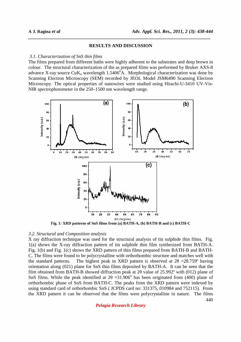
Fig. 1: XRD patterns of SnS films from (a) BATH-A, (b) BATH-B and (c) BATH-C
3.2. Structural and Composition analysis X ray diffraction technique was used for the structural analysis of tin sulphide thin films. Fig. 1(a) shows the X-ray diffraction pattern of tin sulphide thin film synthesized from BATH-A. Fig. 1(b) and Fig. 1(c) shows the XRD pattern of thin films prepared from BATH-B and BATH-C. The films were found to be polycrystalline with orthorhombic structure and matches well with the standard patterns. The highest peak in XRD pattern is observed at 2θ =28.759º having orientation along (021) plane for SnS thin films deposited by BATH-A. It can be seen that the film obtained from BATH-B showed diffraction peak at 2θ value of 25.992º with (012) plane of SnS films. While the peak identified at 2θ =31.906o has been originated from (400) plane of orthorhombic phase of SnS from BATH-C. The peaks from the XRD pattern were indexed by using standard card of orthorhombic SnS ( JCPDS card no: 331375, 010984 and 752115). From the XRD pattern it can be observed that the films were polycrystalline in nature. The films
A J. Ragina et al Adv. Appl. Sci. Res., 2011, 2 (3): 438-444 _____________________________________________________________________________
441 Pelagia Research Library
synthesized from BATH-A and BATH-C were more crystalline than that of BATH-B. There are unidentified peak at 2θ =10o in the case of films from BATH-A and BATH-B. EDAX studies revealed that the films prepared from different host solutions are nearly stoichiometric in nature.
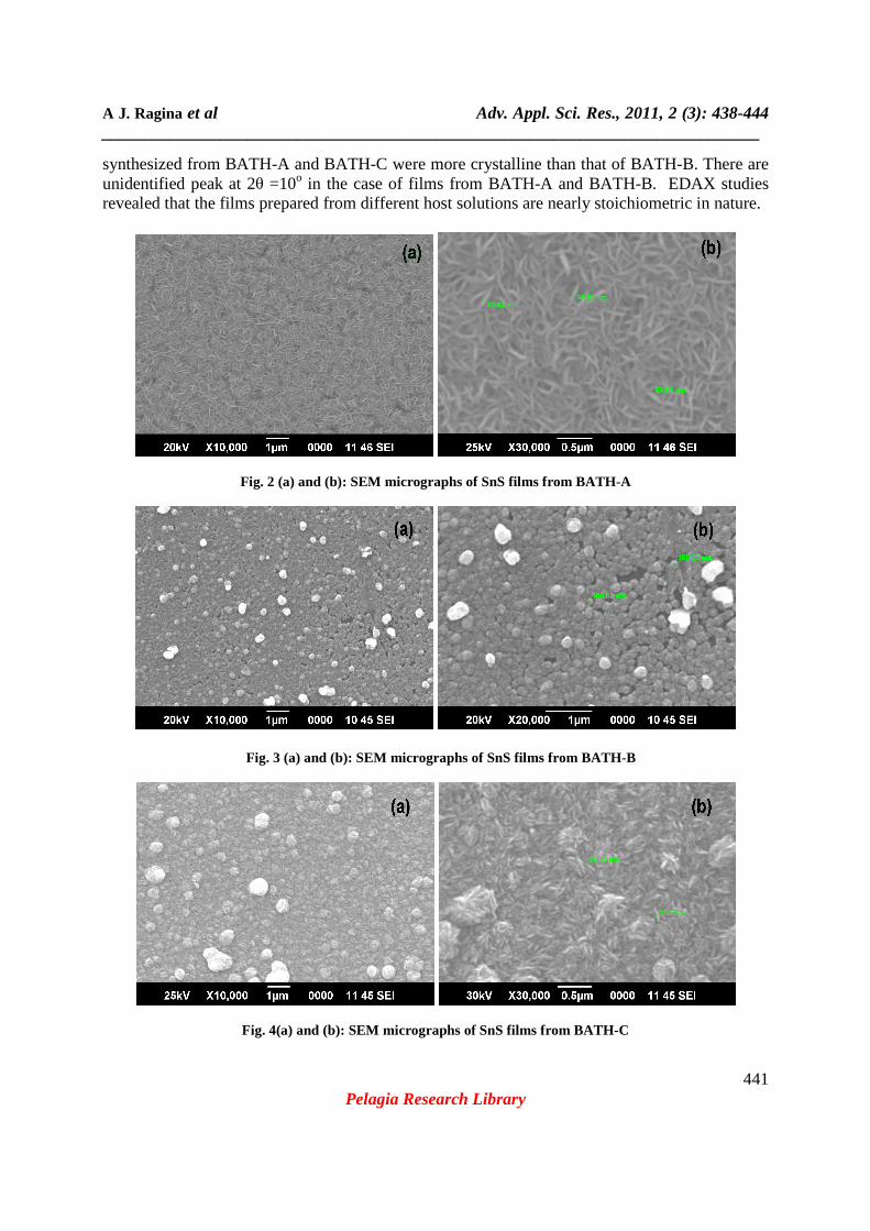
Fig. 2 (a) and (b): SEM micrographs of SnS films from BATH-A
Fig. 3 (a) and (b): SEM micrographs of SnS films from BATH-B
Fig. 4(a) and (b): SEM micrographs of SnS films from BATH-C
A J. Ragina et al Adv. Appl. Sci. Res., 2011, 2 (3): 438-444 _____________________________________________________________________________
442 Pelagia Research Library
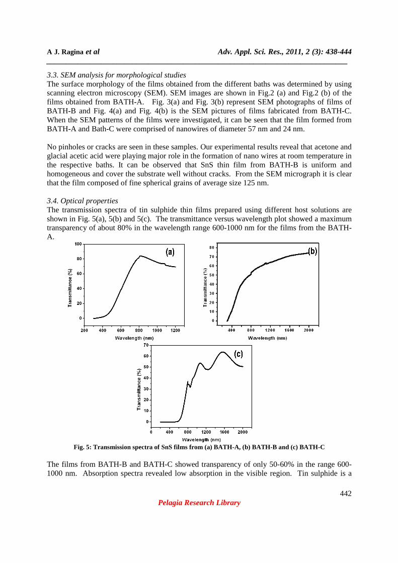
3.3. SEM analysis for morphological studies The surface morphology of the films obtained from the different baths was determined by using scanning electron microscopy (SEM). SEM images are shown in Fig.2 (a) and Fig.2 (b) of the films obtained from BATH-A. Fig. 3(a) and Fig. 3(b) represent SEM photographs of films of BATH-B and Fig. 4(a) and Fig. 4(b) is the SEM pictures of films fabricated from BATH-C. When the SEM patterns of the films were investigated, it can be seen that the film formed from BATH-A and Bath-C were comprised of nanowires of diameter 57 nm and 24 nm. No pinholes or cracks are seen in these samples. Our experimental results reveal that acetone and glacial acetic acid were playing major role in the formation of nano wires at room temperature in the respective baths. It can be observed that SnS thin film from BATH-B is uniform and homogeneous and cover the substrate well without cracks. From the SEM micrograph it is clear that the film composed of fine spherical grains of average size 125 nm. 3.4. Optical properties The transmission spectra of tin sulphide thin films prepared using different host solutions are shown in Fig. 5(a), 5(b) and 5(c). The transmittance versus wavelength plot showed a maximum transparency of about 80% in the wavelength range 600-1000 nm for the films from the BATH-A.
Fig. 5: Transmission spectra of SnS films from (a) BATH-A, (b) BATH-B and (c) BATH-C
The films from BATH-B and BATH-C showed transparency of only 50-60% in the range 600-1000 nm. Absorption spectra revealed low absorption in the visible region. Tin sulphide is a
A J. Ragina et al Adv. Appl. Sci. Res., 2011, 2 (3): 438-444 _____________________________________________________________________________
443 Pelagia Research Library
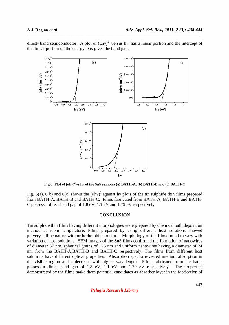
direct- band semiconductor. A plot of (αhν)2 versus hν has a linear portion and the intercept of this linear portion on the energy axis gives the band gap.
Fig.6: Plot of (αhν)2 vs hν of the SnS samples (a) BATH-A, (b) BATH-B and (c) BATH-C
Fig. 6(a), 6(b) and 6(c) shows the (αhν)2 against hν plots of the tin sulphide thin films prepared from BATH-A, BATH-B and BATH-C. Films fabricated from BATH-A, BATH-B and BATH-C possess a direct band gap of 1.8 eV, 1.1 eV and 1.79 eV respectively
CONCLUSION
Tin sulphide thin films having different morphologies were prepared by chemical bath deposition method at room temperature. Films prepared by using different host solutions showed polycrystalline nature with orthorhombic structure. Morphology of the films found to vary with variation of host solutions. SEM images of the SnS films confirmed the formation of nanowires of diameter 57 nm, spherical grains of 125 nm and uniform nanowires having a diameter of 24 nm from the BATH-A,BATH-B and BATH-C respectively. The films from different host solutions have different optical properties. Absorption spectra revealed medium absorption in the visible region and a decrease with higher wavelength. Films fabricated from the baths possess a direct band gap of 1.8 eV, 1.1 eV and 1.79 eV respectively. The properties demonstrated by the films make them potential candidates as absorber layer in the fabrication of
A J. Ragina et al Adv. Appl. Sci. Res., 2011, 2 (3): 438-444 _____________________________________________________________________________
444 Pelagia Research Library
hetero junction solar cells. Also, since the constituent elements of the films are nontoxic and abundant in nature, promotes the development of devices that are environmentally safe.
REFERENCES
[1] K.T.Ramakrishna Reddy and P. Purandhra Reddy, Mate. Lett., 2002, 56,108. [2] R.H. Bube; Photocondutyvity of solids, Wiley, New York, 1960, pp 233. [3] A. Abou Shama, H.M. Zeyada, Opt. Mater. 2003, 24, 555. [4] J. B. Johnson, H. Jones, B. S. Lathan, J. D. Parker, R. D., Engelken and C. Barber, Semicond. Sci. Technol., 1999, 14, 501 [5] A.Ghazali, Z.Zainali, M.Z. Hussein, Kassim, Sol. Energy Mater. Sol. Cells, 1998, 55,237. [6] M.Ichimura, L.Takeuchi, Y.Ono, E. Arail, Thin Solid Films, 2000, 361-362, 98. [7] P. P. Hankare, A. V. Jadhav, P. A. Chate, K. C. Rathod, P. A. Chavan and S. A.. Ingole, J. Alloys Compd., 2008, 463, 581.