zero voltage switching resonant power conversion - · pdf filezero voltage switching resonant...
TRANSCRIPT


Zero Voltage Switching
Resonant Power Conversion
Bill Andreycak
ing zero current, hence zero power switching.And while true, two obvious concerns canin1pede the quest for high efficiency operationwith high voltage inputs.
By nature of the resonant tank and zerocurrent switching limitation, the peak switchcurrent is significantly higher than its squarewave counterpart. In fact, the peak of the fullload switch current is a minimum of twice thatof its square wave kin. In its off state, theswitch returns to a blocking a high voltageevery cycle. When activated by the next drivepulse, the MOSFET output capacitance ( Coss)is discharged by the FET, contributing a signifi-cant power loss at high frequencies and highvoltages. Instead, both of these losses areavoided by implementing a zero voltage switch-
ing technique [9,10].
Zero Voltage Switching OverviewZero voltage switching can best be defined
as conventional square wave power conversionduring the switch's on-time with "resonant"switching transitions. For the most part, it canbe considered as square wave power utilizing aconstant off-time control which varies theconversion frequency, or on-time to maintainregulation of the output voltage. For a givenunit of tin1e, this method is similar to fIXedfrequency conversion which uses an adjustableduty cycle, as shown in Fig. 1.
Regulation of the output voltage is accomp-lished by adjusting the effective duty cycle,performed by varying the conversion frequency, changing the effective on-time in a ZVSdesign. The foundation of this conversion issin1ply the volt-second product equating of theinput and output. It is virtually identical to thatof square wave power conversion, and vastly el
AbstractThe technique of zero voltage switching in
modern power conversion is explored. SeveralZVS topologies and applications, limitations ofthe ZVS technique, and a generalized designprocedure are featured. Two design examplesare presented: a 50 Watt DC/DC converter,and an off-line 300 Watt multiple output powersupply. This topic concludes with a perfor-mance comparison of ZVS converters to theirsquare wave counterparts, and a summary of
typical applications.
IntroductionAdvances in resonant and quasi-resonant
power conversion technology propose alterna-tive solutions to a conflicting set of squarewave conversion design goals; obtaining highefficiency operation at a high switching fre-quency from a high voltage source. Currently,the conventional approaches are by far, still inthe production mainstream. However, anincreasing challenge can be witnessed by theemerging resonant technologies, primarily dueto their lossless switching merits. The intent ofthis presentation is to umavel the details ofzero voltage switching via a comprehensiveanalysis of the timing intervals and relevantvoltage and current waveforms.
The concept of quasi-resonant, "lossless"switching is not new, most noticeably patentedby one individual [1] and publicized by anotherat various power conferences [2,3]. Numerousefforts focusing on zero current switchingensued, fIrst perceived as the likely candidatefor tomorrow's generation of high frequencypower converters [4,5,6,7,8]. In theory, the on-off transitions occur at a time in the resonantcycle where the switch current is zero, facilitat-
Zero Voltage Switching Resonant Conversion 1-1

vSQUAREWAVE R Topp ~
k ..XXBD -JFREQ
0
vzvs
0
Fig. 1- Zero Voltage Switching vs. Conventional Square Wave
Fig. 2 -Resonant Switch Implementation
SWITCH -
~ OPP I 0. I OPP r-;;;-0. OPP 0. OPP OBacTIvATIoB
i iI II II II IIVIW-
VO1- VCR IO -
o
Fig. 3- Genera/ Wavefonns
unlike the energy transfer system of its electri-cal dual, the zero current switched converter .
During the ZVS switch off-time, the L-Ctank circuit resonates. This traverses the volt -age across the switch from zero to its peak,and back down again to zero. At this point theswitch can be reactivated, and lossless zerovoltage switching facilitated. Since the outputcapacitance of the MOSFET switch (Coss) hasbeen discharged by the resonant tank, it doesnot contribute to power loss or dissipation inthe switch. Therefore, the MOSFET transitionlosses go to zero -regardless of operatingfrequency and input voltage. This could repre-sent a significant savings in power, and result ina substantial improvement in efficiency. obvi-ously, this attribute makes zero voltage switch-ing a suitable candidate for high frequency,high voltage converter designs. Additionally, thegate drive requirements are somewhat reducedin a ZVS design due to the lack of the gate todrain (Miller) charge, which is deleted whenV DS equals zero.
The technique of zero voltage switching isapplicable to all switching topologies; the buckregulator and its derivatives (forward, half andfull bridge), the flyback, and boost converters,to name a few. This presentation will focus onthe continuous output current, buck derivedtopologies, however a list of references describ-ing the others has been included in the appen-dix.
zvs Benefits
.Zero power " Lossless " switching transitions
.Reduced EMI / RFI at transitions
.No power loss due to discharging Coss
.No higher peak currents, (ie. ZCS) same assquare wave systems
.High efficiency with high voltage inputs at
any frequency
.Can incorporate parasitic circuit and compo-nentL&C
1-2 UNITRODE CORPORATION

.Reduced gate drive requirements (no"Miller" effects)
.Short circuit tolerant
fIlter section consisting of output inductor Loand capacitor Co has a time constant severalorders of magnitude larger than any powerconversion period. The fIlter inductance is largein comparison to that of the resonant inductor'svalue LR and the magnetizing current MLo aswell as the inductor's DC resistance is negligi-ble. In addition, both the input voltage VlN andoutput voltage Vo are purely DC, and do notvary during a given conversion cycle. Last, theconverter is operating in a closed loop configu-ration which regulates the output voltage Vo .
Initial Conditions: Time interval < toBefore analyzing the individual time inter-
vals, the initial conditions of the circuit must bedeflDed. The analysis will begin with switch Qlon, conducting a drain current ID equal to theoutput current Io, and VDs = VCR = O (ideal).
In series with the switch Ql is the resonantinductor LR and the output inductor Lo whichalso conduct the output current Io .It has beenestablished that the output inductance Lo islarge in comparison to the resonant inductorLR and all components are ideal. Therefore, thevoltage across the output inductor V Lo equalsthe input to output voltage differential; V Lo =
VlN -Vo .The output filter section catch diodeDo is not conducting and sees a reverse voltageequal to the input voltage; V Do = Vl, observing
the polarity shown in Figure 4.
Table I. INITIAL CONDITIONS
COMP. STATUS
01 ON
Do OFF
LA
Lo
zvs Differences:
.Variable frequency operation (in general)
.Higher off-state voltages in single switch,
unclamped topologies
.Relatively new technology -users must climbthe learning curve
.Conversion frequency is inversely propor-tional to load current
.A more sophisticated control circuit may be
required
ZVS Design EquationsA zero voltage switched Buck regulator
will be used to develop the design equationsfor the various voltages, currents and timeintervals associated with each of the conversionperiods which occur during one completeswitching cycle. The circuit schematic, compo-nent references, and relevant polarities areshown in Fig. 4.
Typical design procedure guidelines and"shortcuts" will be employed during the anal-ysis' for the purpose of brevity. At the onset,all components will be treated as though theywere ideal which simplifies the generation ofthe basic equations and relationships. As thissection progresses, losses and non-ideal charac-teristics of the components will be added to theformulas. The timing summary will expoundupon the equations for a precise analysis.
Another valid assumption is that the output
CIRCUIT VALUES
VDS=VCR=O; ID=ILR=ILO=lo
VDO=VIN; IDO=O
ILR=IO ; VLR=O
V, r)=VIN-VO ; ILO=O
Vo
Capacitor Charging State: to -t 1The conversion period is initiated at time to
when switch QI is turned OFF. Since thecurrent through resonant inductor LR andoutput inductor Lo cannot change instanta-neously, and no drain current flows in QI while
Fig. 4 -Zero Voltage Switched Buck Regulator
1-3Zero Voltage Switching Resonant Conversion

Table II -CAPACITOR CHARGING: to -tl
Fig. 5 -Simplified Model
CRV1N
10
tOl =
IcR = /0for (0« «1
Fig. 6- Resonant Capacitor Wavefonns
COMP. STATUS CIRCUIT VALUES
01 OFF ID=O; VDS(t)=VCR(t)
CR Charging ICR=O ; VCR(t) RISES UNEARLY
VCR(tO)=O; VCR(t1)=VIN
LR ILR(t)=IO;VLR=ODO OFF VDO(tO)=VIN ; VOQ(t1)=O ;
DECREASES UNEARLY
Lo VLQ(tO)=VIN-VO ; VLO(t1)=-VODECREASES UNEARLY ; ILO=lo
Resonant State: tl -t2The resonant portion of the conversion cycle
begins at t 1 when the voltage across resonantcapacitor V CR equals the input voltage V IN' andthe output catch diode begins conducting- Att I, current through the resonant componentsIcR and ILR equals the output current 10.
The stimulus for this series resonant L-Ccircuit is output current 10 flowing through theresonant inductor prior to time ti. The ensuingresonant tank current follows a cosine functionbeginning at time ti' and ending at time t2- Atthe natural resonant frequency "'R, each of theL-G tank components exhibit an impedanceequal to the tank impedance, ZR- Therefore,the peak voltage across GR and switch Ql are afunction of ZR and 10.
The instantaneous voltage across GR and Qlcan be evaluated over the resonant time inter-val using the following relationships:
/0
it is off, the current is diverted around theswitch through the resonant capacitor CR. Theconstant output current will linearly increasethe voltage across the resonant capacitor untilit reaches the input voltage (V CR = v IN). Since
the current is not changing, neither is thevoltage across resonant inductor LR.
At time to the switch current ID "instantly"drops from 10 to zero. Simultaneously, theresonant capacitor current IcR snaps from zeroto 10, while the resonant inductor current ILRand output inductor current ILO are constantand also equal to 10 during interval tOr .Voltageacross output inductor Lo and output catchdiode D o linearly decreases during this intervaldue to the linearly increasing voltage acrossresonant capacitor CR. At time t1' V CR equalsV IN' and Do starts to conduct.
v CR(rl) = V1NZR = l/U)RCR
:. v CR(t) = V'N+loZR sin[c.> R(t-tJ]:~
Of greater importance is the ability to solvethe equations for the precise off-time of theswitch. This off-time will vary with line andload changes and the control circuit mustrespond in order to facilitate true zero voltageswitching. While some allowance does exist fora fIXed off time technique, the degree of lati-
UNITRODE CORPORATION1-4

tude is insufficient to accommodate typicalinput and output variations. The exact time isobtained by solving the resonant capacitorvoltage equations for the condition when zerovoltage is attained.
Let V CR(t) = 0 ; IoZR SIN(.> R(t-tJ) = -V1N
LINE CHANGES
The equation can be further simplified byextracting the half cycle (180 degrees) of con-duction which is a constant for a given resonantfrequency, and equal to 1\" /CUR .
,'2V1Nt 1\" 1 .
12 = -+ -arcsm
C.>R C.>R
Fig. 8 -Resonant Capacitor Voltage vs. Load
to maintain a constant output current 10. Itsreverse voltage is clamped to the output voltageVo minus the diode voltage drop V DO by theconvention followed by Figure 4.
Table III -RESONANT INTERV AL: tl .~
COMP. STATUS CIRCUIT VALUES
01 OFF VOS(t)=VCA(t)
CA Resonant VCA(t) =VIN + (loZAsin(IJA(t-t1)))IcA(t) = IOcos(wA(t-t1))
LA Resonant VLA(t) = [loZAsin(wA(t-t1))ILA(t) = ICA(t)
Do ON IOQ(t) = IO-ILA(t)
Lo Discharge VLO=-(VO+VOO(fwd))
~ z-'0 R Jr1
The resonant component current (IcR = ILR)
is a cosine function between time t 1 and t2'described as:
ICR(I) = Iocos[U) R(t-tJ]:~
The absolute maximum duration for thisinterval occurs when 270 degrees (311" /2UJ~ ofresonant operation is required to intersect thezero voltage axis. This corresponds to the limitof resonance as minimum load and maximumline voltage are approached.
Contributions of line and load influences onthe resonant time interval t]2 can be analyzedindividually as shown in Figs. 7 and 8.
Prior to time tl' the catch diode Do was notconducting. Its voltage, V 00' was linearly de-creasing from V IN at time to to zero at ti whileinput source V IN was supplying full outputcurrent, Io. At time tl' however, this situationchanges as the resonant capacitor initiatesresonance, diverting the resonant inductorcurrent away from the output filter section.Instantly, the output diode voltage, V 00' chang-es polarity as it begins to conduct, supplement-ing the decreasing resonant inductor currentwith diode current loo. extracted from storedenergy in output inductor Loo The diode cur-rent waveshape follows a cosine function duringthis interval, equalling Io minus IcR(t).
Also occurring at time tl' the output fIlterinductor Lo releases the stored energy required
Zero Voltage Switching Resonant Conversion 1-5
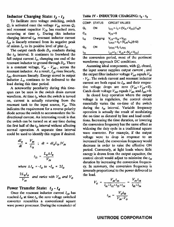
Table IV .INDUCTOR CHARGING: t2 -t3
COMP. STATUS CIRCUIT VALUES
01 ON lo(t)=-lo+((VIN+VOO)/LA)t
CA VCA=O
LA Charging VLA=VIN+VOOILA(t) = -10 + (V LA/LA) (t-t2)
Do ON IOO(t) = 10-ILA(t)
Lo ILO=IO; VLO=-(VO+VOO)
the conversion period, most of the pertinent
waveforms approach DC conditions.
Assuming ideal components, with QJ closed,
the input source supplies output current, and
the output filter inductor voltage V LO equals VlN
-V 0. The switch current and resonant inductor
current are both equal to 10, and their respec-
tive voltage drops are zero (VDs=VLR=O).
Catch diode voltage V DO equals VlN, and lDO=O.
In closed loop operation where the output
voltage is in regulation, the control circuit
essentially varies the on-time of the switch
during the tJ4 interval. Variable frequency
operation is actually the result of modulating
the on-time as dictated by line and load condi-
tions. Increasing the time duration, or lowering
the conversion frequency has the same effect as
widening the duty cycle in a traditional square
wave converter. For example, if the output
voltage were to drop in response to an
increased load, the conversion frequency would
decrease in order to raise the effective ON
period. Conversely, at light loads where little
energy is drawn from the output capacitor, the
control circuit would adjust to minimize the tJ4
duration by increasing the conversion frequen-
cy. In summary, the conversion frequency is
inversely proportional to the power delivered to
the load.
Inductor Charging State: t2 -t3To facilitate zero voltage switching, switch
Ql is activated once the voltage V DS across Qland resonant capacitor V CR has reached zero,occurring at time t2. During this inductorcharging interval tv resonant inductor currentI LR is linearly returned from its negative peakof minus 10 to its positive level of plus 10.
The output catch diode D 0 conducts duringthe t2J interval- It continues to freewheel thefull output current 10, clamping one end of theresonant inductor to ground through D 0- Thereis a constant voltage, VlN -V DO , across theresonant inductor. As a result, ILR rises linearly,100 decreases lineatly. Energy stored in outputinductor Lo continues to be delivered to theload during this time period.
A noteworthy peculiarity during this time-span can be seen in the switch drain currentwaveform. At time t2' when the switch is turnedon, current is actually returning from theresonant tank to the input source, VlN- Thisindicates the requirement for a reverse polaritydiode across the switch to accommodate the bi-directional current. An interesting result is thatthe switch can be turned on at any time duringthe first half of the t2J interval without affectingnormal operation. A separate time intervalcould be used to identify this region if desired.
~=~dl
; dl = dIRLR /V/N
LR
LR6.IR
V1N
(23 =
where tJ.IR = -10 to +10 = 210
2LRlo
VlNand varies with V1N and Vo
~N 134
Im+134
V1N (34Vo = =
tO1 +(12+ (23 + (34
Power Transfer State: 13 -14Once the resonant inductor current I LR has
reached 10 at time tj, the zero voltage switchedconverter resembles a conventional squarewave power processor. During the remainder of
VOt03
~
(34 =
UNITRODE CORPORATION

Table V- POWER TRANSFER: t] -t4
COMP. STATUS
01 ON
CR
~
Do OFF
Lo Charging
CIRCUIT VALUES
VOS = IoRoS(ON) ; 10 = 10
VCR=O
ILR=lo; VLR=O
VOo=VIN
VLO=VIN-Vo; ILO=lo
~N=18VVo = 5 V
10 = 5 A
Fig. 9 --ZVS Buck Regulator Wavefonns
Zero Voltage Switching Resonant Conversion 1-7

2LRlomin
~Nmar
:. 123 = = 2
C.>R
t34min = 0
zvs Converter Limitations:In a ZVS converter operating under ideal
conditions, the on-time of the switch «(23+(34)approaches zero, and the converter will operateat maximum frequency and deliver zero outputvoltage. In a practical design , however, theswitch on-time cannot go to zero for severalreasons.
First of all, the resonant tank componentsare selected based on the maximum inputvoltage ~Nmox and minimum output currentIOmin for the circuit to remain resonant over alloperating conditions of line and load. If thecircuit is to remain zero voltage switched, thenthe resonant tank current cannot be allowed togo to zero. It can, however, reach 10min .
There is a finite switch on-time associatedwith the inductor charging interval (23 where theresonant inductor current linearly increasesfrom -10 to + 10. As the on-time in the powertransfer interval (J4 approaches zero, so will theconverter output voltage. Therefore, the mini-mum on-time and the maximum conversionfrequency can be calculated based upon thelimitation of 10min and zero output voltage.
The limits of the four zero voltage switchedtime intervals will be analyzed when 10 goes to10 minimum. Each solution will be retained interms of the resonant tank frequency CUR for
generalization.
1+1.51\"
CUR
0.909
fR
Maximum Off-Time:
tOl+t12min = =
The maximum conversion frequency corre-sponds to the minimum conversion period,T CONVmi" , which is the sum of the minimum on-time and maximum off-time:
T CONVmi,,:
311'
2(,,)R
1.511"
t.)R
tl2max = =
F CONVmax
fR
f R /1.227
~ZR
WR
~Nmax
Iominw R
KTmax = = 0.815=LR = =
1-8 UNITRODE CORPORATION

conversion period where (34 equals zero. Topol-ogy coefficient KT will be incorporated todefme the ratio of the maximum conversionfrequency (minimum conversion period) to thatof the resonant tank frequency, WR.
~N = POTCONV ' Where TCONV = ~WR
V/~Iomin7.71 -WIN = p Omin-;:;- -2U> R VINmax
R
ViNlomin
2(7.71)V1Nmax
p Omin = VOlomin
Fig. 10-- WaVefonnS atFCONV = Kr.fR
In a realistic application, the output voltageof the power supply is held in regulation at Vowhich stipulates that the on-time in the powerprocessing state, t 34 , cannot go to zero as inthe example above. The volt-second product re-quirements of the output must be satisfiedduring this period, just as in any square waveconverter design. Analogous to minimum dutycycle, the minimum on-time for a given designwill be a function of V1N, V o and the resonanttank frequency, UJR.
Although small, a specific amount of energyis transferred from the input to the outputduring the capacitor charging interval tOI. Thevoltage into the output fIlter section linearlydecreases from V1N at time to to zero at tl'equal to an average value of V1N/2. In addition,a constant current equal to the output current/0 was being supplied from the input source.The average energy transferred during thisinterval is defined as:
p Omin = 0.065 V/Nmaxlomin ; :::: 6.5% PINmin
21 ViNIo CR ViN ViNCR
WIN = -ViNIotOt = --= -
2 2 10 2
The equation can be reorganized in terms of
CR and "'R as:
Under normal circumstances the circuit willbe operating far above this minimum require-ment, In most applications, the amount ofpower transferred during the capacitor charginginterval tOl can be neglected as it representsless than seven percent (7% ) of the minimuminput power, This corresponds to less than onepercent of the total input power assuming alO:lload range,
ZVS Effective Duty Cycles:A valid assumption is that a negligible
amount of power is delivered to the loadduring the capacitor charging interval tol' Also,no power is transferred during the resonantperiod from tn' Although the switch is onduring period t2J, it is only recharging the
V/~Iomin~N 2U) R V/Nmax
This minimum energy can be equated tominimum output watts by dividing it by its
Zero Voltage Switching Resonant Conversion 1-9

resonant and output inductors to maintain theminimum output current, 10..-". In summary,NO output power is derived from ~N duringinterval tm.
The power required to support V o at itscurrent of 10 is obtained from the input sourceduring the power transfer period t 34. Therefore,an effective "duty cycle" can be used to de-scribe the power transfer interval t 34 to that ofthe entire switching period, t04' or T CONV .
ZVS .Effective Duty Cycle Calculations:
V t"Duty Cycle" = -.£. = ~
V1N t()4
could optionally be evaluated.A computer program to calculate the numer-
ous time intervals and conversion frequenciesas a function of line and load can simplify thedesign process, if not prove to be indispensable.Listed in the Appendix of this section is aBASIC language program which can be used toinitiate the design procedure.
To summarize: When the switch is on, re-place V1N with (V1N-VDS(011) = (V1N-Io.RDS(oll).
When the free-wheeling diode is on, replace V owith (V 0+ VF).
t -CR (~N-IoRDS(oll»01 -
10134"Duty Cycle" =
VINIlItU- ROS(on)IOminZR ---IOmin
Transformer Coupled Circuit Equa-
tions:The general design equations for the Buck
topology also apply for its derivates; namely theforward, half-bridge, full-bridge and push-pullconverters. Listed below are the modificationsand circuit specifics to apply the previousequations to transformer coupled circuits.General Transformer Coupled Circuits. MaiDt-aiDing the resonant tank components on theprimary side of the transformer isolation boun-dary is probably the most common and sim-plest of configurations. The design procedurebegins by transforming the output voltage andcurrent to the primary side through the turnsratio, N. The prime (') designator will be usedto signify the translated variables as seen by theprimary side circuitry.
tO1 +t12+ t23 +t34
And can be analyzed over line and loadranges using previous equations for each inter-val.
Accommodating wsses in the Design
Equations:Equations for zero voltage switching using
ideal components and circuit parameters havebeen generated, primarily to understand eachof the intervals in addition to computer model-ing purposes. The next logical progression is tomodify the equations to accommodate voltagedrops across the components due to seriesimpedance, like RDS(oll)' and the catch diodeforward voltage drop. These two represent themost significant loss contributions in the buckregulator model. Later, the same equations willbe adapted for the buck derived topologieswhich incorporate a transformer in the power
stage.The procedure to modify the equations is
straightforward. Wherever VrN appears in theequations while the switch is on it will bereplaced by VrN- V DS(oll) , the latter being afunction of the load current /0. The equationscan be further adjusted to accept changes ofRDS(011) and V F , etc. with the device junctiontemperatures. Resonant component initialtolerances, and temperature variations likewise
1-10 UNITRODE CORPORATION

Primary TurnsN=Secondary Turns
Io'=Io/N; Vo'=Vo.N ; and Zo'=Zo.N2
To satisfy the condition for resonance, IR<Io'
The resonant tank component equations nowbecome:
ZR
(NR
L =R
=V1N1IWX N
Iominw R
Determining Transformer Turns Ratio (N):The transformer turns ratio is derived from theequations used to derme the power transferinterval t34 in addition to the maximum off-time, t03. While this may rust seem like aniterative process, it simplifies to the volt-secondproduct relationship described. The generalequations are listed below.
The turns ratio N is derived by substitutingN. Vo for the output voltage Vo in the powertransfer interval t34 equation. Solving for Nresults in the relationship:
NVO/V1N = t34/(tOl+t12+t23+t3J
V1Nmin t34N=Note: the calculated resonant inductancevalue does not include any series inductance,typical of the transformer leakage and wiringinductances.
VOt04
The transformer magnetizing and leakageinductance is part of the resonant inductance.This requires adjustment of the resonant induc-tor value, or both the resonant tank impedanceZR and frequency (J)R will be off-target. One
Iomin
NV1NmaxC.> R
CR = -;;--1
Note: the calculated resonant capacitor valuedoes not include any parallel capacitance,typical of a MOSFET output capacitance, Coss,in shunt. Multi-transistor variations of the bucktopology should accommodate all switch capaci-tances in the analysis.
Timing Equations (including N):
CRV1NN
10[ ] 12 1 .V1NN
+ -arcsm -
(J) R IoZR 11
11"
U}R
2LRlo
~ option is to design the transformer inductanceto be exactly the required resonant inductance,thus eliminating one component. For precisionapplications, the transformer inductance shouldbe made slightly smaller than required, and"shimmed" up with a small inductor.
NVO(tOl+tI2+t23)
VJN-NVO
T CONY = /Ol +/12+/23+/34
1.11Zero Voltage Switching Resonant Conversion

Expanding zvs to Other Topologies
ZVS Forward Converter -Single Ended:The single ended forward converter can easilybe configured for zero voltage switching withthe addition of a resonant capacitor across theswitch. Like the buck regulator, there is a highvoltage excursion in the off state due to reso-nance, the amplitude of which varies with lineand load. The transformer can be designed sothat its magnetizing and leakage inductanceequals the required resonant inductance. Thissimplifies transformer reset and eliminates onecomponent. A general circuit diagram is shownin Fig. 12 below. The associated waveforms forwhen LpRI equals LR are shown in Fig. 13.
LSHIM
Fig. 13 -Forward Convelter Wavefonns
1-12 UNITRODE CORPORATION

zvs Clamped Configurations 00 Half and
Full Bridge Topologies: Zero voltage switchingcan be extended to multiple switch topologiesfor higher power levels, specifically the half andfull bridge configurations. While the basicoperation of each time interval remains similar,there is a difference in the resonant t12 interval.
While single switch converters have high off -
state voltage, the bridge circuits clamp theswitch peak voltages to the DC input rails,reducing the switch voltage stress. This altersthe duration of the off segment of the resonantinterval, since the opposite switch(es) must beactivated long before the resonant cycle is com-pleted. In fact, the opposite switch( es ) shouldbe turned on immediately after their voltage isclamped to the rails, where their drain tosource voltage equals zero. If not, the resonanttank will continue to ring and return the switchvoltage to its starting point, the opposite rail.Additionally, this off period varies with line andload changes.
Examples of this are demonstrated in Figs.14 and 15. To guarantee true zero voltageswitching, it is recommended that the necessarysense circuitry be incorporated. Fig. 15 --C/amped ZVS Wavefonns
1-13Zero Voltage Switching Resonant Conversion

Fig. 16 --ZVS Half Bridge Circuit
tO tlt2 tJ t. tO tl t2 tJ
ON
OFF
0.
0"
VIN
VIN
zvs Half Bridge: The sameturns ratio, N, relationshipapplies to the half bridge to-pology when V1N in the previ-ous equations is considered tobe one-half of the bulk rail-to-rail voltage. ~N is the voltageacross the transformer primarywhen either switch is on.
Refer to the circuit andwaveforms of Figs. 14 and 15.CR, the resonant capacitorbecomes the parallel combina-tion of the two resonant capac-itors, the ones across eachswitch. Although the resonantinductor value is unaffected, allseries leakage and wiring in-ductance must be taken intoaccount.
The off state voltages of theswitches will try to exceed theinput bulk voltage during theresonant stages. Automaticclamping to the input bulkrails occurs by the MOSFETbody diode, which can beexternally shunted with a high-er performance variety. Unlikethe forward converter whichrequires a core reset equal tothe applied volt second prod-uct, the bidirectional switchingof the half ( and full) bridgetopology facilitate automaticcore reset during consecutive
switching cycles [11,12].
2
a
VIN
!.!!12
O
10N rT!r0
~
10N
..-
~
IOUT
-V Dl
t~O
IOUT
-VD2
0 ---t t-- '--r--.
! ! ! ! ! : : i: !tO tl t2 t3 t( tO tl t2 t3
tOtl t2 t3 t.
Fig. 17 --ZVS Ha/f Bridge Wavefonns
1-14 UNITRODE CORPORATION

zvs Full Bridge: The equa-tions represented for the for-ward topology apply equallywell for one conversion cycleof the full bridge topology,including the transformer turnsratio. Since the resonant ca-pacitors located at each switchare "in-circuit" at all times,the values should be adjustedaccordingly. As with the halfbridge converter, the resonantcapacitors' voltage will exceedthe bulk rails, and clamping viathe FET body diodes or exter-nal diodes to the rails is com-mon [13].
Fig. 18 -ZVS Full Bridge Circuit
to tlt2 tJ t. tO tl t2 tJ
ON
OFF
ON
orr
VIN
,,,--~~ ,
\.~ r J'j
v": ..~-c
~".JA--n..VIN 0:
!,
0
r-~:;;.l i.~ f ,
IoN
~ i
:
0
-10N
~
IOUT
-V Dl
~
IOUT
-VD2
Ot
..
tO tl t2 tJ
-~- ---i ---l--.: : : : : :1 I I I C , , I
: : : : : :
t4 tO tl t2 t3
tOtl t2 t3 t.
Fig. 19 -ZVS Full Bridge Wavefonns
1-15Zero Voltage Switching Resonant Conversion

zvs Design Procedure
Buck Derived Topologies 00 ContinuousOutput Current:
1. List all input/output specs and ranges.
~N min & max ; V o ; 10 min & max
8. Breadboard the circuit carefully using RFtechniques wherever possible. Remember --
parasitic inductances and capacitances preferto resonate upon stimulation, and quite
often, unfavorably.
9. Debug and modify the circuit as required toaccommodate component parasitics, layoutconcerns or packaging considerations.
Avoiding ParasiticsRinging of the catch diode junction capaci-
tance with circuit inductance (and packageleads) will significantly degrade the circuitperformance. Probably the most commonsolution to this everyday occurrance in squarewave converters is to shunt the diode with anR-C snubber. Although somewhat dissipative,a compromise can be established betweensnubber losses and parasitic overshoot causedby the ringing. Unsnubbed examples of variousapplicable diodes are shown in Fig. 20 below.
Estimate the maximum switch voltages. For
unclamped applications (buck and forward):
V DSIOWJX = V1NIOWJX(1 + (lolOWJX/lo",;,,)
Note: Increase lo",;" if V DSIOWJX is too high if
possible).
For clamped applications (bridges):
V DSIOWJX= ~NIOWJX
3. Select a resonant tank frequency, wR
(HINT: wR=21ffR).
4. Calculate the resonant tank impedance andcomponent values.
5. Calculate each of the interval durations (tOIthru (34) and their ranges as a function of allline and load combinations.(See Appendix -for a sample computerprogram written in BASIC)
Additionally, summarize the results to estab-lish the range of conversion frequencies,peak voltages and currents, etc.
6. Analyze the results. Determine if the fre-quency range is suitable for the application.If not, a recommendation is to limit the loadrange by raising [om;" and start the designprocedure again. Verify also that the designis feasible with existing technology and
components.
7. Finalize the circuit specifics and details.
D Derive the transformer turns ratio. (non-buck applications)
D Design the output fIlter section based uponthe lowest conversion frequency and output
ripple currentJo(ac).D Select applicable components; diode,
MOSFET etc.
1-16 UNITRODE CORPORATION
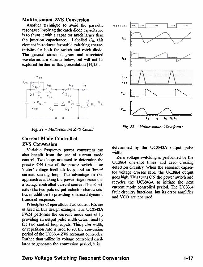
Multiresonant ZVS ConversionAnother technique to avoid the parasitic
resonance involving the catch diode capacitanceis to shunt it with a capacitor much larger thanthe junction capacitance. Labelled CD, thiselement introduces favorable switching charac-teristics for both the switch and catch diode.The general circuit diagram and associatedwaveforms are showm below, but will not beexplored further in this presentation [14,15].
loo
VCK
VDS
L-~~
IDO
VDO-/"L ~
t o ~ ~ ~ t4
Fig. 22 --Multiresonant WavefonnsFig. 21 --Multiresonant ZVS Circuit
determined by the UC3843A output pulsewidth.
Zero voltage switching is performed by theUC3864 one-shot timer and zero crossingdetection circuitry. When the resonant capaci-tor voltage crosses zero, the UC3864 outputgoes high. This turns ON the power switch andrecyctes the UC3843A to initiate the nextcurrent mode controlled period. The UC3864fault circuitry functions, but its error amplifierand VCO are not used.
Current Mode Controlled
ZVS ConversionVariable frequency power converters can
also benefit from the use of current modecontrol. Two loops are used to determine theprecise ON time of the power switch --an"outer" voltage feedback loop, and an "inner"current sensing loop. The advantage to thisapproach is making the power stage operate asa voltage controlled current source. This elimi-nates the two pole output inductor characteris-tics in addition to providing enhanced dynamictransient response.
Principles or operation. Two control ICs areutilized in this design example. The UC3843APWM performs the current mode control byproviding an output pulse width determined bythe two control loop inputs. This pulse width,or repetition rate is used to set the conversionperiod of the UC3864 ZVS resonant controller.Rather than utilize its voltage controlled oscil-lator to generate the conversion period, it is
Zero Voltage Switching Resonant Conversion 1-17

zvs Forward Converter ..DesignExample
Table VI .Interval Durations vs. Line & Load
VIN=18 VIN=18 VIN=26 VIN=2610=2.5 10= 10 10=2.5 10= 10
t10 0.217 0.055 0.314 0.078t12 1.29 1.06 1.49 1.08t23 0.93 3.72 0.64 2.58t34 1.39 6.68 0.78 1.78TCONV 3.83 11.51 3.23 5.52fCONV 261kHz 87kHz 310kHz 181kHz
Transistor Switch Durations:
toN 2.32 10.4 1.42 4.36toFF 1.51 1.11 1.80 1.16
1. List circuit specifications:
VI!\, = 18 to 26 VV o = 5.0 V; 10 = 2.5 to 10 A
2. Estimate the maximum voltage across theswitch:
V DSmax= VINmax(l + (IOmtU/IOmi,,»
=26-(1+(10/2.5» = 26-5 = 130 V
~~
r.:i~H~
T.DO..A
~~--::::~-...'"."'..,, --
-..A
3. Select a resonant tank frequency, wR.
A resonfiDt tank period frequency of SOOKHzwill be used. It was selected as a compro-mise between high frequency operation andlow parasitic effects of the components and
layout.
fR = SOOKHz ; ~ =3.14.106 radians/sec
I I I I I18 20 22 2. 26
VrN(VOLTB)
Fig. 23 -Switch Times vs. Line & Load
dfcONV/d~N vs 10
10 = 2.SA SA 7.SA 10A avg
df/dV = 6.1 11.211.9 11.7 10.2
Highest "gain" (11.9 kHz/V) occurs near full
load.
4. Calculate the resonant tank impedance andcomponent values.
Resonant tank impedance, ZR > V1Nmax/IOmin
To accommodate the voltage drop across theMOSFET, calculate V DS(on)min' which equalsRDS(on!Omin = 0.8.2.5 = 2V
ZR = (V1Nmax-VDSmin)/IOmin
ZR = (26-2)/2.5 = 10 O
CR = l/(Z#~ = 1/(10.3.14.106) = 32nF
LR = ZR/C.>R = 10/3.34 .106 = 3.18p.HdfcONV/dlo vs VlN
VlN = 18 20 22 24 26 avg
df/dV = 23.3 22.1 20.5 18.8 17.3 20.4
Highest "gain" (23.3 kHz/A) occurs at VlNmin.
5. Calculate each or the interval durations (tOlthru t.u> and ranges as they vary with lineand load changes.
The zero voltage switched buck converter"gain" in kiloHertz per volt of ~N and kHzper amp of 10 can be evaluatated over thespecified ranges. A summary of these fol-lows:
It may be necessary to use the highest gainvalues to design the control loop compensationfor stability over all operating conditions. Whilethis may not optimize the loop transient re-sponse for all operating loads, it will guaranteestability over the extremes of line and load.
1.18 UNITRODE CORPORATION
L 1LO
98765432~0
~
3S0K-...= 300K-
>- 2S0~-'-'
= 200K -!::)O 1.50K -..,~...1.00E -
75E -
OA
..-SA ~
~~7..A
~---
~
I20 22 24
VI:N(VOLTS)
Fig. 24 -Conversion Freq. vs. Line & Load
6. Analyze the results.
The resonant component values, range ofconversion frequencies, peak voltage andcurrent ratings seem well within the practicallimits of existing components and technology.
7. Finalize the circuit specifics and detailsbased on the information obtained above.
A. Output Filter Section: Select Lo and Cofor operation at the lowest conversionfrequency and designed ripple current.
B. Heatsink Requirements: An estimate ofthe worst case power dissipation of thepower switch and output catch diode can bemade over line and load ranges.
C. Control Circuit: The UC3861-64 series ofcontrollers will be examined and pro-grammed per the design requirements.
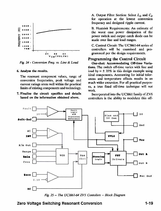
Programming the Control CircuitOne-sbot: Accommodating OIT-time Varia-
tions. The switch off-time varies with line andload by::= ::t 35% in this design example usingideal components. Accounting for initial toler-ances and temperature effects results in anmuch wider excursion. For all practical purpos-es, a true fIXed off-time technique will notwork.
Incorporated into the UC3861 family of ZVScontrollers is the ability to modulate this off-
rault
Logicand
Precision
Reference
-,.sv
Bias andSV Gen~
8oft fl
Gnd
NI
In 1JVI.O
~ Vcc
B/A Out
Range
..la
Cvco
Out a~.'1'
Drivers8'..aSa,
Logic
~
Out B
I.~o PWE Gnd
ac
Fig. 25 --The UC3861-64 ZVS Contollers --Block Diagram
Zero Voltage Switching Resonant Conversion 1-19

VCR
lated range of conversion frequencies spans 87to 310 kHz. These values will be used for this"fIrst cut" draft of the control circuit pro-grantming. Due to the numerous circuit specif -
ics omitted from the computer program forsimplicity, the actual range of conversion fre-quencies will probably be somewhat wider thanplanned. Later, the actual timing componentvalues can be adjusted to accommodate thesedifferences.
First, a minimum fc of 75 kHz has beenselected and programmed according to the
following equation:
F~Omi" = 3.6/(Rmi"C~o)
The maxim um f c of 350 kHZ is programmed
f- TOFF VARIATIONS ~
111 111
-CR Volts & Off-time vs. Line & Load
by:FK'Omar = 3.6/(Rmin I Rra"8") 0 CK'O
Numerous values of Rmin and CK'O will satisfythe equations. The procedure can be simplifiedby letting Rmin equal looK.
CK'O (JJ.F) = O.O36/fmin (kHz)
RRANGE (kO) = loo/(fcoNVmar/fcONVmin -1)
where Rmin=looK, CK'O=470pF,RRANGE = 27K
The VCO gain in frequency per volt fromthe error amplifier output is approximated by:
dF/dV = 1/(RRANGEC\-t:'o) = 78.2 kHz/V
with an approximate 3.6 volt delta from theerror amplifier .
time. Initially, the one-shot is programmed forthe maximum off-time, and modulated via theZERO detection circuitry. The switch drain-source voltage is sensed and scaled to initiateturn-on when the precision 0.5V threshold iscrossed. This offset was selected to accommo-date propogation delays between the instant thethreshold is sensed and the instant that theswitch is actually turned on. Although brief,these delays can become significant in highfrequency applications, and if left unaccounted,can cause NONZERO switching transitions.
Referring to Fig. 26, in this design, the off -
time varies between 1.11 and 1.80 microsec-onds, using ideal components and neglectingtemperature effects on the resonant compo-nents. Since the ZERO detect logic will facili-tate "true" zero voltage switching, the off-timecan be set for a much greater period,Th h t h 31 bil 'ty VOLTAGE CONTROLLED OSCILLATOR
e one-s o as a: range capa 1 E/Aand will be programmed for 2,2 uS
~(max), controllable down to 0.75 uS. +
Programming of the one-shot requires .
a single R-C time constant, and isstraightforward using the design infor- Omation and equations from the data ..
sheet. Implementation of this feature isshown in the control circuit schematic,
[
aAHGB
~ [
NIB
-=? -=-=- rFig. 27 --E/A -VCO B/ock DiagramProgramming the VCO. The calcu-
UNITRODE CORPORATION

FAULT ~f I
Fig. 29 --Fault Operational Wavefonns
Fault Protection -Soft Start & RestartDelay: One of the unique features of the UC3861 family of resonant mode controllers canbe found in its fault management circuitry. Asingle pin connection interfaces with the softstart, restart delay and programmable faultmode protection circuits. In most applications,one capacitor to ground will provide full pro-tection upon power-up and during overloadconditions. Users can reprogram the timingrelationships or add control features (latch offfollowing fault, etc) with a single resistor .
Selected for this application is a 1 uP soft-restart capacitor value, resulting in a soft -startduration of 10 ms and a restart delay of ap-proximately 200 ms. The preprogrammed ratioof 19:1 (restart delay to soft start) will be uti-lized, however the relevant equations andrelationships have also been provided for otherapplications. Primary current will be utilized asthe fault trip mechanism, indicative of anoverload or short circuit current condition. Acurrent transformer is incorporated to maxi-mize efficiency when interfacing to the threevolt fault threshold.
Optional Programming of T ss and T RD :
Soft Start: Tss = CsR.10K
Restart Delay: T RD = CsR.l90K
Timing Ratio: T RD:T ss ~ 19:1
Gate Drive: Another unique feature of theUC 3861-64 family of devices is the optimalutilization of the silicon devoted to outputtotem pole drivers. Each controller uses twopins for the A and B outputs which are inter-nally configured to operate in either unison orin an alternating configuration. Typical perfor-mance for these 1 Amp peak totem pole out-puts shows 30 ns rise and fall times into 1nF .
Loop Compensation --General Information.The ZVS technique is similar to that of con-ventional voltage mode square wave conversionwhich utilizes a single voltage feedback loop.Unike the dual loop system of current modecontrol, the ZVS output fIlter section exhibits
a two pole-zero pair and is compensated ac-cordingly. Generally, the overall loop is de-signed to cross zero dB at a frequency belowone-tenth that of the switching frequency. Inthis variable frequency converter, the lowestconversion frequency will apply, correspondingto approximately 85 KHz, for a zero crossing of8.5 KHz. Compensation should be optimizedfor the highest low frequency gain in additionto ample phase margin at crossover. Typicalexamples utilize two zeros in the error amplifi-er compensation at a frequency equal to that ofthe output filter's two pole break. An addition-al high frequency pole is placed in the loop tocombat the zero due to the output capacitanceESR, assuming adequate error amplifier gain-bandwidth.
A noteworthy alternative is the use of a twoloop approach which is similar to current modecontrol, eliminating one of the output poles.One technique known as Multi-Loop Controlfor Quasi-Resonant Converters [18] has been
Zero Voltage Switching Resonant Conversion 1-21
developed. Another, called Average CurrentMode Control is also a suitable candidate.
1 1fU = .fU =PI ~ ' ZI ( D lID 'rR R \CFP F I.flFP IIflnJ F
1;
(R1P+Ra>C1
1R;C;
C.>Z2=CUn =
RFP IIRn
R1P+Rrz
Gain at !ZI' !Z2 =
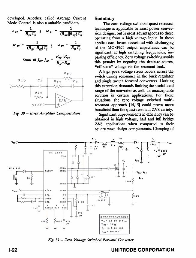
SummaryThe zero voltage switched quasi-resonant
technique is applicable to most power conver-sion designs, but is most advantageous to thoseoperating from a high voltage input. In theseapplications, losses associated with dischargingof the MOSFET output capacitance can besignificant at high switching frequencies, im-pairing efficiency. Zero voltage switching avoidsthis penalty by negating the drain-to-source,"off-state" voltage via the resonant tank-
A high peak voltage stress occurs across theswitch during resonance in the buck regulatorand single switch forward converters. Limitingthis excursion demands limiting the useful loadrange of the converter as well, an unacceptablesolution in certain applications. For thesesituations, the zero voltage switched multi-resonant approach [14,15] could prove morebeneficial than the quasi-resonant ZVS variety.
Significant improvements in efficiency can beobtained in high voltage, half and full bridgeZVS applications when compared to theirsquare wave design complements. Clamping of
Fig. 30 -EITor Amplifier Compensation
Le~ V..T
: -~ +1
1 Cell::o1 =
VI. ILa La TI
> t 1I1~ ~II~100 .1 La
11 uP -Dor~.,~
IpO
f-t-\ 1-~~T2l,lOO
--t:*- 1 Ve.-VDo
le.~'11.2.:
-Voa.
~~.~,°.,
65~
lUpr
11°El1up
1 .70
-=- pP
;J.oOK I "lO pP
Fig. 31 --Zero Voltage Switched Forward Converter
UNITRODE CORPORATION1-22

the peak resonant voltage to the input railsavoids the high voltage overshoot concerns ofthe single switch converters, while transforD1erreset is accomplished by the bidirectionalswitching. Additionally, the series transforD1erprimary and circuit inductances can beneficial,additives in the formation of the total resonantinductor value. This not only reduces size, butincorporates the detrimental parasitic generallysnubbed in square wave designs, further en-
hancing efficiency.
A new series of control ICs has been devel-oped specifically for the zero voltage switchingtechniques with a list of features to facilitatelossless switching transitions with completefault protection. The multitude of functions andease of programmability greatly simplify theinterface to this new generation of powerconversion techniques; those developed inresponse to the demands for increased powerdensity and efficiency.
Zero Voltage Switching Resonant Conversion 1-23

[12] R. Steigerwald, " A Comparison of Half-
Bridge Resonant Converter Topologies,"IEEE 1987
[13] J. Sabate, F. C. Lee, "Offline Applicationof the Fixed Frequency Clamped ModeSeries-Resonant Converter," IEEEAPECConference, 1989
[14] W. Tabisz, F. C. Lee, "Zero Voltage-Switching Multi-Resonant Technique -aNovel Approach to Improve Performanceof High Frequency Quasi-Resonant con-verters," IEEE PESC, 1988
[15] W. Tabisz, F. C. Lee, " A Novel, Zero-
Voltage Switched M ulti- Resonant ForwardConverter," High Frequency Power Con-ference, 1988
[16] L. Wofford, " A New Family of Integrated
Circuits Controls Resonant Mode PowerConverters," Power Conversion andIntelligent Motion Conference, 1989
[17] W. Andreycak, "Controlling Zero VoltageSwitched Power Supplies," High Frequen-cy Power Conference, 1990
[18] R. B. Ridley, F. C. Lee, V. Vorperian,"Multi-Loop Control for Quasi-ResonantConverters, " High Frequency Power Con-
ference Proceedings, 1987
Additional References:
."High Frequency Resonant, Quasi-Resonantand Multi-Resonant Converters," VirginiaPower Electronics Center, (Phone # 703-961-4536), Edited by Dr. Fred C. Lee
."Recent Developments in Resonant PowerConversion," Inteltec Communication Press(Phone # 805-658-0933), Edited by K KitSum
References[1] P. Vinciarelli, "Forward Converter
Switching At Zero Current, " U.S. Patent
# 4,415,959 (1983)[2] K. H. Liu and F. C. Lee, " Resonant
Switches -a Unified Approach to Im-proved Performances of Switching Con-verters," 1ntemalional Telecommumica-lions Energy Conference; New Orleans,1984
[3] K. H. Lieu, R. Oruganti, F. C. Lee, "Res-onant Switches -Topologies and charac-teristics," IEEE PESC 1985 (France)
[4] M. Jovanovic, D. Hopkins, F. C. Lee,"Design Aspects For High FrequencyOff-line Ouasi-resonant Converters," HighFrequency Power Conference, 1987
[5] D. Hopkins, M. Jovanovic, F. C. Lee, F.Stephenson, "Two Megahertz Off-LineHybridized Ouasi-resonant Converter,"IEEE APEC Conference, 1987
[6] W. M. Andreycak, "1 Megahertz 150Watt Resonant Converter Design Review,Unitrode Power Supply Design SeminarHandbook SEM-6OOA, 1988
[7] A. Heyman, "Low Profile High Frequen-cy Off-line Ouasi Resonant Converter,"IEEE 1987
[8] W. M. Andreycak, "UC3860 ResonantControl IC Regulates Off-Line 150 WattConverter Switching at 1 MHz, " High
Frequency Power Conference 1989
[9] M. Schlect, L. Casey, "Comparison of theSquare-wave and Ouasi-resonant Topolo-gies," IEEE APEC Conference, 1987
[10] M. Jovanovic, R. Farrington, F. C. Lee,"Comparison of Half-Bridge, ZCS-ORCand ZVS-MRC For Off-Line Applica-tions," IEEE APEC Conference, 1989
[11] M. Jovanovic, W. Tabisz, F. C. Lee, "Ze-ro Voltage-Switching Technique in High-Frequency Off-Line Converters," IEEEPESC, 1988
1-24 UNITRODE CORPORATION

10 ' Zero Voltage Switching Calculations and Equations20 ' Using the Continuous Current Buck Topology30 ' in a Typical DC/DC Converter Power Supply Application
40'50 PRINTER$ = "lptl:": ' Printer at parallel port #1 **********60 ,70 ' Summary of Variables and Abbreviations
80'90 ' Cr = Resonant Capacitor
lOO' Lr = Resonant Inductor110' Zr = Resonant Tank Impedance120 ' Fres = Resonant Tank Frequency (Hz)130 ,140 ' Vlmin = Minimum DC Input Voltage150 ' Vlmax = Maximum DC Input Voltage160 ' Vdson = Mosfet on Voltage = 10*Rds170 ' Rds = Mosfet on Resistance180 ' Vdsmax = Peak MOSFET off State Voltage190 ' Vo = DC output Voltage200 ' V do = Output Diode Voltage Drop210 ' 10max = Maximum Output Current220 ' 10min = Minimum Output Current
230'240 ' Start with parameters for low voltage dc/dc buck regulator250 ,260 ' ****Define 5 Vi and 5 10 data points ranging from min to max*'270 ' (Suggestion: With broad ranges, use logarithmic spread)
280 DATA 18,20,22,24,27 : 'Vi data290 DATA 2.5,4,6,8,10 : '10 data300 FRES = 500000!310 VO = 5!320 V DO = .8330 RDS = .8340 SAFT = .95350 ,
360 FOR J = 1 TO 5: READ VI(J): NEXT370 FOR K = 1 TO 5: READ 10(K): NEXT
380 CLS390 PRINT "For OUtput to screen, enter'S' or'S',"400 INPUT "Otherwise output will be sent to printer: ", K$410 IF K$ = "5" OR K$ = "s" THEN K$ = "scrn:" ELSE K$ = PRINTER$
420 OPEN K$ FOR OUTPUT AS #1: CLS430 PRINT #1, "================================================"440 PRINT #1, " Zero Voltage Switching Times (uSec) vs. Vi, 10"
450 PRINT #1, "================================================"460 ,
1-A1Zero Voltage Switching Resonant Conversion

470 ' =========HERE GOES===========
480 ,
490 VIMAX = VI(5): 10MIN = 10(1): 10MAX = 10(5)500 ZR = (VIMAX -(RDS * 10MIN)) / (IOMIN * SAFT)
510 WR = 6.28 * FRES
520 CR = 1/ (ZR * WR)
530 LR = ZR / WR540 ,
550 FOR J = 1 TO 5: VI = VI(J)
560 PRINT #1, USING" Input Voltage = ###.## V"; VI
570 FOR K = 1 TO 5: 10 = 10(K)580 RSIN = (VI/ (IO * ZR)): VDSON = RDS * 10
590 ,
600 D(O, K) = 10 * .000001: ' Compensate for later mult. by 10-6
610 D(l, K) = (CR * VI) / 10: 'dt01620 D(2, K) = (3.14/ WR) + (1/ WR) * ATN(RSIN / (1 -RSIN A 2)): 'dt12
630 D(3, K) = (2 * LR * 10) / VI: 'dt23
640 D(6, K) = D(l, K) + D(2, K) + D(3, K): ' dt03
650 D(4, K) = «VO + VDO) * D(6, K)) / «VI -VDSON) -(VO + VDO)): 'dt34
660 D(5, K) = D(l, K) + D(2, K) + D(3, K) + D(4, K): 'Tconv
670 NEXT K680 ,
690 PAR$(O) = "la (A) ="
700 PAR$(l) = "dt01 ="
710 PAR$(2) = "dt12 ="
720 PAR$(3) = "dt23 ="
730 PAR$(4) = "dt34 ="
740 PAR$(5) = "Tconv ="
750 PAR$(6) = "dt03 ="760 ,
770 FOR P = 0 TO 6
780 PRINT #1, PAR$(P);790 FOR K = 1 TO 5800 PRINT #1, USING" ####.###"; D(P. K) * l000000!;
810 NEXT K: PRINT #1,
820 NEXT P
830 PRINT #1,
840 NEXT J850 ,
860 PRINT #1, "Addit;onal Informat;on:"870 PRINT #1. "Zr(Ohms) ="; INT(1000! * ZR) /1000
880 PRINT #1, "wR(KRads)="; INT(WR / 1000)890 PRINT #1, "Cr(nF) ="; INT«1000 * CR) /10 --9) /1000900 PRINT #1, "Lr(uH) ="; INT«1000 * LR) / 10 A -6) / 1000
910 PRINT #1, "Vdsmax ="; VIMAX * (1 + 10MAX / 10MIN)
920 END
1-A2 UNITRODE CORPORATION

Zero Voltage Switching Times (uSec) vs. Vi, 10
Input Voltage = 18.00 V
2.500 4.000 6.000 8.0000.218 0.136 0.091 0.0681.290 1.153 1.096 1.0700.931 1.490 2.235 2.9801.387 1.791 2.682 4.1183.825 4.571 6.103 8.2362.439 2.780 3.421 4.118
10.0000.0541.0563.7256.677
11.5114.835
10 (A) =
dtO1
dt12
dt23
dt34TCOnV =
dtO3
Input Voltage = 20.00 V2.500 4.000 6.000 8.0000.242 0.151 0.101 0.0761.339 1.175 1.108 1.0790.838 1.341 2.011 2.6821.150 1.406 1.987 2.8523.569 4.074 5.207 6.6882.419 2.667 3.220 3.836
10.0000.0611.0623.3524.1868.6614.475
10 (A) =
dtO1dt12
dt23
dt34TCOnV =
dtO3
Input Voltage = 22.00 V
2.500 4.000 6.000 8.0000.266 0.166 0.111 0.0831.390 1.198 1.120 1.0870.762 1.219 1.829 2.4380.988 1.153 1.557 2.1363.406 3.737 4.616 5.7442.418 2.584 3.060 3.608
10.0000.0671.0693.0482.9587.1414.183
10 (A) =
dtO1
dt12
dt23
dt34TCOnV =
dtO3
Input Voltage = 24.00 V2.500 4.000 6.000 8.0000.290 0.182 0.121 0.0911.442 1.223 1.133 1.0960.698 1.117 1.676 2.2350.870 0.975 1.268 1.6823.301 3.498 4.199 5.1032.431 2.522 2.930 3.421
10.0000.0731.0752.7942.2416.1833.941
10 (A) =
dtO1
dt12
dt23
dt34TCOnV =
dtO3
Input Voltage = 27.00 V
2.500 4.000 6.000 8.0000.327 0.204 0.136 0.1020.516 1.264 1.153 1.1090.621 0.993 1.490 1.9870.442 0.793 0.983 1.2531.906 3.254 3.763 4.4511.464 2.461 2.780 3.198
10.0000.0821.0852.4831.6045.2543.650
10 (A) =
dtO1
dt12
dt23
dt34TCOnV =
dtO3
Additional Information:Zr(Ohms) = 10.526
wR(KRads)= 3140Cr(nF) = 30.254
Lr(uH) = 3.352
Vdsmax = 135
1-A3Zero Voltage Switching Resonant Conversion

IMPORTANT NOTICE
Texas Instruments and its subsidiaries (TI) reserve the right to make changes to their products or to discontinueany product or service without notice, and advise customers to obtain the latest version of relevant informationto verify, before placing orders, that information being relied on is current and complete. All products are soldsubject to the terms and conditions of sale supplied at the time of order acknowledgment, including thosepertaining to warranty, patent infringement, and limitation of liability.
TI warrants performance of its products to the specifications applicable at the time of sale in accordance withTI’s standard warranty. Testing and other quality control techniques are utilized to the extent TI deems necessaryto support this warranty. Specific testing of all parameters of each device is not necessarily performed, exceptthose mandated by government requirements.
Customers are responsible for their applications using TI components.
In order to minimize risks associated with the customer’s applications, adequate design and operatingsafeguards must be provided by the customer to minimize inherent or procedural hazards.
TI assumes no liability for applications assistance or customer product design. TI does not warrant or representthat any license, either express or implied, is granted under any patent right, copyright, mask work right, or otherintellectual property right of TI covering or relating to any combination, machine, or process in which suchproducts or services might be or are used. TI’s publication of information regarding any third party’s productsor services does not constitute TI’s approval, license, warranty or endorsement thereof.
Reproduction of information in TI data books or data sheets is permissible only if reproduction is withoutalteration and is accompanied by all associated warranties, conditions, limitations and notices. Representationor reproduction of this information with alteration voids all warranties provided for an associated TI product orservice, is an unfair and deceptive business practice, and TI is not responsible nor liable for any such use.
Resale of TI’s products or services with statements different from or beyond the parameters stated by TI forthat product or service voids all express and any implied warranties for the associated TI product or service,is an unfair and deceptive business practice, and TI is not responsible nor liable for any such use.
Also see: Standard Terms and Conditions of Sale for Semiconductor Products. www.ti.com/sc/docs/stdterms.htm
Mailing Address:
Texas InstrumentsPost Office Box 655303Dallas, Texas 75265
Copyright 2001, Texas Instruments Incorporated