zinc oxide nanostructures: synthesis and properties · 2017-09-27 · zinc oxide nanostructures:...
TRANSCRIPT

1
Zinc Oxide Nanostructures: Synthesis and Properties
Zhiyong Fan and Jia G. Lu*
Department of Chemical Engineering and Materials Science & Department of Electrical Engineering and Computer Science
University of California, Irvine, CA 92697, USA
This article provides a comprehensive review of the current research activities that focus on the ZnO nanostructure materials and their physical property characterizations. It begins with the synthetic methods that have been exploited to grow ZnO nanostructures. A range of remarkable characteristics are then presented, organized into sections describing the mechanical, electrical, optical, magnetic and chemical sensing properties. These studies constitute the basis for developing versatile applications of ZnO nanostructures. Keywords: wide band gap semiconductor; nanostructure; UV emission; field effect transistors, chemical sensing; spintronics
Submission: 7 January, 2005 Revised/Accepted: 22 April, 2005
CONTENTS 1. Introduction 2. Synthesis of ZnO Nanostructures
2.1 Vapor Transport Synthesis 2.2 Patterned Growth and Vertical Alignment of ZnO Nano-Array 2.3 Other Growth methods
3. Physical Properties of ZnO Nanostructures 3.1 Mechanical Properties 3.2 Piezoelectric effect and polar surfaces 3.3 Electrical Properties 3.4 Optical Properties 3.5 Magnetic Doping 3.6 Chemical Sensing
4. Conclusions
*Author to whom correspondence should be addressed. Email: [email protected]


1
1. Introduction Zinc oxide (ZnO), a wide bandgap (3.4 eV) II-VI compound semiconductor, has a stable wurtzite structure with lattice spacing a = 0.325 nm and c = 0.521 nm. It has attracted intensive research effort for its unique properties and versatile applications in transparent electronics, ultraviolet (UV) light emitters, piezoelectric devices, chemical sensors and spin electronics.1-10 Invisible thin film transistors (TFTs) using ZnO as an active channel have achieved much higher field effect mobility than amorphous silicon TFTs.11-13 These transistors can be widely used for display applications. ZnO has been proposed to be a more promising UV emitting phosphor than GaN because of its larger exciton binding energy (60 meV). This leads to a reduced UV lasing threshold and yields higher UV emitting efficiency at room temperature.14 Surface acoustic wave filters using ZnO films have already been used for video and radio frequency circuits. Piezoelectric ZnO thin film has been fabricated into ultrasonic transducer arrays operating at 100 MHz.15 Bulk and thin films of ZnO have demonstrated high sensitivity for toxic gases.16-19 Furthermore, hole mediated ferromagnetic ordering in bulk ZnO by introducing Mn as dopant has been predicted theoretically 20 and reported recently.21 Vanadium doped n-type ZnO films also demonstrate a Curie temperature above room temperature.22 Based on these remarkable physical properties and the motivation of device miniaturization, large effort has been focused on the synthesis, characterization and device applications of ZnO nanomaterials. An assortment of ZnO nanostructures, such as nanowires, nanotubes, nanorings, and nano-tetrapods have been successfully grown via a variety of methods including chemical vapor deposition, thermal evaporation, and electrodeposition, etc. 23-32 These nanostructures have been subjected to electrical transport, UV emission, gas sensing, and ferromagnetic doping studies, and considerable progresses have been achieved.33 This review presents recent advances on ZnO nanostructures. Issues of synthesis methods, structural, electrical, optical, magnetic and gas sensing properties are summarized. 2. Synthesis of ZnO Nanostructures 2.1 Vapor Transport Synthesis
The most common method to synthesize ZnO nanostructures utilizes a vapor transport process. In such a process, Zn and oxygen or oxygen mixture vapor are transported and react with each other, forming ZnO nanostructures. There are several ways to generate Zn and oxygen vapor. Decomposition of ZnO is a direct and simple method, however, it is limited to very high temperatures (~1400°C).34 Another direct method is to heat up Zn powder under oxygen flow.35,36 This method facilitates relative low growth temperature (500~700°C), but the ratio between the Zn vapor pressure and oxygen pressure needs to be carefully controlled in order to obtain desired ZnO nanostructures. It has been observed that the change of this ratio contributes to a large variation on the morphology of nanostructures.35 The indirect methods to provide Zn vapor include metal-organic vapor phase epitaxy, in which organometallic Zn compound, diethyl-zinc for example, is used under appropriate oxygen or N2O flow.23,37-41 Also in the widely used carbothermal method,14,42-69 ZnO powder is mixed with graphite powder as source material. At about 800-1100 °C, graphite reduces ZnO to form Zn and CO/CO2 vapors. Zn and CO/CO2 later react and result in ZnO nanocrystals. The advantages of

2
this method lie in that the existence of graphite significantly lowers the decomposition temperature of ZnO.
According to the difference on nanostructure formation mechanisms, the extensively used vapor transport process can be categorized into the catalyst free vapor-solid (VS) process and catalyst assisted vapor-liquid-solid (VLS) process. Synthesis utilizing VS process is usually capable of producing a rich variety of nanostructures, including nanowires, nanorods, nanobelts and other complex structures.29-31,34,50-64 In a typical VS process, complex ZnO nanostructures such as nanohelixes and nanobelts were synthesized by Kong et al.34 (Fig. 1a & b). In this process, ZnO powder was decomposed into Zn2+ and O2- at ~1350 °C, then under Ar carrier gas, nanostructures were deposited onto an alumina substrate at a low temperature zone (400-500 °C). In a similar vapor transport and condensation process reported by Ren et al.,50,51,63 hierarchical ZnO nanostructures, as shown in Fig. 1c, were grown by heating mixed powder of ZnO, In2O3 and graphite to 820-870 °C. A simplified method to achieve nanowires, nanoribbons and nanorods was reported by Yao et al.52, in which ZnO powder was mixed with graphite and heated to 1100 °C. After cooling down, nanostructures were found to form on the wall of the furnace. Fig. 1d shows the needle-like ZnO rods. Fig. 1. (a) A SEM micrograph of ZnO nanohelix structures grown via VS process. (b) A TEM image of ZnO nanobelt grown via VLS process. Inset: structure model of the nanobelt. Reprint from ref. 34, X. Y. Kong et al., Nano. Lett. 3, 1625 (2003) with permission from American Chemical Society. (c) Hierachical ZnO nanostructures synthesized by vapor transport and condensation technique. Scale bar: 10 µm. Reprint from ref. 50, J. Y. Lao et al., Nano. Lett. 2, 1287 (2002) with permission from American Chemical Society. (d) Needle-like ZnO rods. Reprint from ref. 52, B. D. Yao et al., Appl. Phys. Lett. 81, 757 (2002) with permission from American Institute of Physics.
(a)
(d)
(b)
3
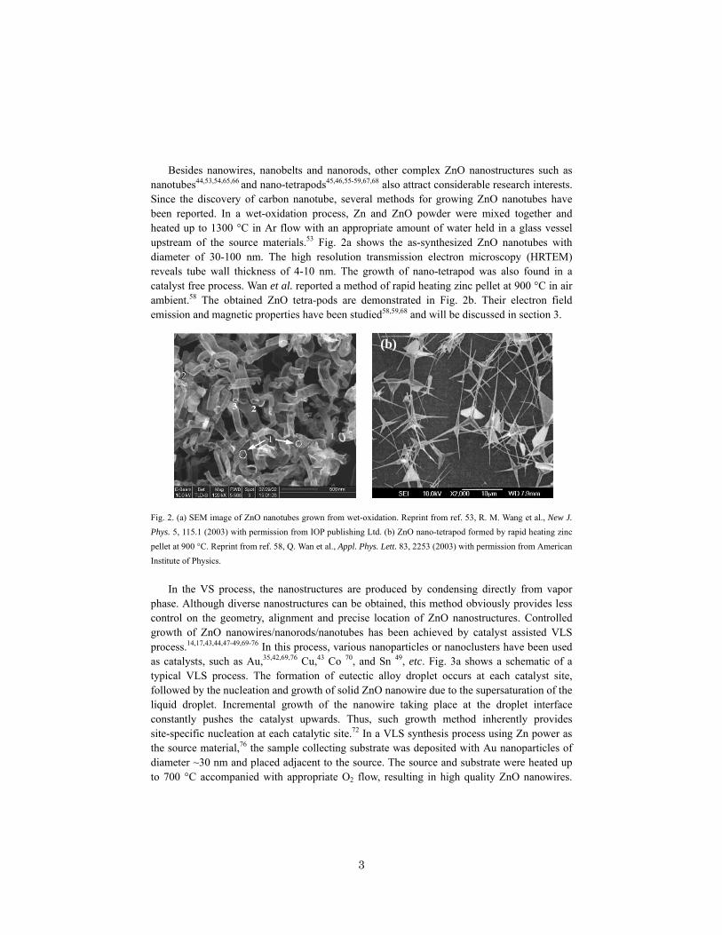
Besides nanowires, nanobelts and nanorods, other complex ZnO nanostructures such as
nanotubes44,53,54,65,66 and nano-tetrapods45,46,55-59,67,68 also attract considerable research interests. Since the discovery of carbon nanotube, several methods for growing ZnO nanotubes have been reported. In a wet-oxidation process, Zn and ZnO powder were mixed together and heated up to 1300 °C in Ar flow with an appropriate amount of water held in a glass vessel upstream of the source materials.53 Fig. 2a shows the as-synthesized ZnO nanotubes with diameter of 30-100 nm. The high resolution transmission electron microscopy (HRTEM) reveals tube wall thickness of 4-10 nm. The growth of nano-tetrapod was also found in a catalyst free process. Wan et al. reported a method of rapid heating zinc pellet at 900 °C in air ambient.58 The obtained ZnO tetra-pods are demonstrated in Fig. 2b. Their electron field emission and magnetic properties have been studied58,59,68 and will be discussed in section 3.
Fig. 2. (a) SEM image of ZnO nanotubes grown from wet-oxidation. Reprint from ref. 53, R. M. Wang et al., New J. Phys. 5, 115.1 (2003) with permission from IOP publishing Ltd. (b) ZnO nano-tetrapod formed by rapid heating zinc pellet at 900 °C. Reprint from ref. 58, Q. Wan et al., Appl. Phys. Lett. 83, 2253 (2003) with permission from American Institute of Physics.
In the VS process, the nanostructures are produced by condensing directly from vapor
phase. Although diverse nanostructures can be obtained, this method obviously provides less control on the geometry, alignment and precise location of ZnO nanostructures. Controlled growth of ZnO nanowires/nanorods/nanotubes has been achieved by catalyst assisted VLS process.14,17,43,44,47-49,69-76 In this process, various nanoparticles or nanoclusters have been used as catalysts, such as Au,35,42,69,76 Cu,43 Co 70, and Sn 49, etc. Fig. 3a shows a schematic of a typical VLS process. The formation of eutectic alloy droplet occurs at each catalyst site, followed by the nucleation and growth of solid ZnO nanowire due to the supersaturation of the liquid droplet. Incremental growth of the nanowire taking place at the droplet interface constantly pushes the catalyst upwards. Thus, such growth method inherently provides site-specific nucleation at each catalytic site.72 In a VLS synthesis process using Zn power as the source material,76 the sample collecting substrate was deposited with Au nanoparticles of diameter ~30 nm and placed adjacent to the source. The source and substrate were heated up to 700 °C accompanied with appropriate O2 flow, resulting in high quality ZnO nanowires.
(b)

4
(c)
The SEM image of the as-synthesized nanowires with uniform diameters is shown in Fig. 3b. The inset SEM micrograph demonstrates that a ZnO nanowire terminates with a Au nanoparticle, which is a clear indication of the VLS process. HRTEM study (Fig. 3c) suggests that the nanowires grow along the [0001] direction, where the epitaxy energy is minimized. Based on the VLS mechanism, the diameter of nanowires can be tuned by using different sizes of nanoparticles or nanocluster catalysts.14 In addition, the control of nanowire growth location and alignment has been realized by using patterning techniques and choosing proper epitaxy substrates. These issues will be further discussed in the next section.
Fig. 3. (a) Schematic of VLS process. (b) SEM image of mesh of ZnO nanowires grown via VLS process. Inset: a ZnO nanowire with diameter of 35 nm and terminated with an Au nanoparticle. (c) High resolution TEM image of a ZnO nanowire shows growth direction along [0001].
2.2 Patterned Growth and Vertical Alignment of ZnO Nano-Array
The application prospect of ZnO nanostructures largely relies on the ability to control their location, alignment and packing density. As mentioned above, they have been achieved by catalyst assisted VLS synthesis process. To control the locations of ZnO nanowires, both lithographic and non-lithographic patterning techniques have been utilized. With photolithography technique,73 square and hexagonal catalytic gold dot array was generated on sapphire substrate, then small diameter ZnO nanowires were grown from the patterned
(b)
Catalyst nanoparticle Alloy with Zinc
ZnO precipitation uponsupersaturation
Nanowire growth
Zn vapor
O2O2
(a)

5
catalysts via a typical VLS process, as shown in Fig. 4a. A simple way to create patterned catalysts array is to use shadow masks for catalyst deposition. For example, TEM grids were used to pattern square Au matrix.74 Fig. 4b shows the resulting ZnO nanowire array. It is out of question that well-ordered and high density ZnO nanowires array can be obtained using advanced lithographic technique such as electron beam lithography. In fact, this objective can be also realized by simply using non-lithographic shadow mask. Chik et al. have successfully fabricated hexagonal ZnO nanorod array by using anodic aluminum oxide membranes (AAM) as a mask to pattern Au catalyst on GaN substrate.72 In this work, a 500 nm thick AAM was carefully attached to a GaN substrate. After evaporation of Au, hexagonal catalyst dot array functioned as nanowire growth sites and resulted in the highly ordered ZnO nanowires array as shown in Fig. 4c.
(a)
(b)
(c)

6
Fig. 4. (a) Hexagonal ZnO nanowire array generated by lithographically patterned Au catalysts. Reprint from ref. 73, E. C. Greyson et al., Adv. Mater. 16, 1348 (2004) with permission from Wiley-VCH Verlag GMBH & Co.. (b) Square ZnO nanowires array created using TEM grids. Reprint from ref. 74, H. J. Fan et al., Supperlattice Microst. 36, 95 (2004) with permission from Elsevier. (c) Hexagonal ZnO nanorod array with diameter ~60 nm and spacing ~110 nm. Reprint from ref. 72, H. Chik et al., Appl. Phys. Lett. 84, 3376 (2004) with permission from American Institute of Physics.
Vertical aligned ZnO nanowires/nanorods have promising applications such as electron field emitter, vertical transistor and UV laser, thus have attracted enormous attention.14,37,47,48,66,77-79 Ng et al. demonstrated ZnO nanowire based vertical field effect transistor with surround gate.47 In their work, the positions of nanowires were controlled via lithographic patterning technique. Vertical aligned ZnO nanowires were observed to grow from lithographically patterned Au spots (Fig. 5a). These nanowires were later surrounded with SiO2 and Cr which function as the gate oxide and gate electrode, as depicted in the inset of Fig. 5a. Using AAM to fabricate metallic and semiconducting nanowire/nanotube array has been widely investigated. It was shown above that the highly ordered vertical ZnO nanowire array had been obtained by a non-lithographic AAM based second-order self-assembly of ZnO nanorods.72 Another unique non-lithographic method to grow vertical aligned ZnO nanowire array combines monolayer self-assembly and VLS nanostructure growth.48 In this method, submicron polystyrene spheres were self-assembled on sapphire )0112( substrate to form a monolayer, then they functioned as a shadow mask for evaporation of catalytic metal (Au), yielding a highly ordered hexagonal array of gold spots. After etching away the polystyrene spheres using toluene, the substrate was placed in a thermal furnace and undergone a VLS synthesis with ZnO powder and graphite powder as source.
Although the vertical alignment of ZnO nanostructures can be assisted by an electric field,80 in most cases, the alignment is realized by lattice matching between ZnO and the substrate. Several types of epitaxy substrates have been utilized, including sapphire,14,48,74 GaN,37,60,61,72,74 ZnO film coated substrate,71 SiC 47 and Si substrate.81-84 Yang et al. have grown vertical aligned ZnO nanowires array on sapphire )0211( plane, as shown in Fig. 5b. The photoluminescence and lasing property of the nanowires array were investigated. Apparently the quality of vertical alignment is mainly determined by the lattice mismatch between ZnO and the supporting substrate. Table 1 gives the crystal structures, lattice parameters and mismatch between ZnO (0001) plane and several epitaxy substrates. Though sapphire has been widely used as the epitaxy substrate for vertical growth of ZnO nanowires, it can be seen that GaN could be an even better candidate since it has the same crystal structure and similar lattice constants to that of ZnO. This has been confirmed by the work of Fan et al.,74 in which both the sapphire a-plane and GaN (0001) plane were used as epitaxy layer for ZnO nanowire growth. Fig. 6 demonstrates the corresponding results. The nanowires grown on GaN epilayer show better vertical alignment than those on sapphire. The additional advantage of employing GaN as epilayer instead of sapphire and ZnO rests in the fact that GaN has much better electrical property than Al2O3 and it is much easier to be doped to p-type than ZnO. This implies the potential of fabricating n-ZnO/p-GaN nanoscale heterojunctions. In fact, this structure has been implemented in ZnO nanorod electroluminescence device.37

7
Fig. 5. (a) 45° view of an array of individual ZnO nanowires grown from Au catalyst spots. Scale bar: 1 µm. Inset: schematic of a ZnO nanowire vertical transistor. Reprint from ref. 47, H. T. Ng et al., Nano. Lett. 4, 1247 (2004) with permission from American Chemical Society. (b) Vertical aligned ZnO nanowires array on sapphire substrate. Reprint from ref. 14, P. Yang et al., Adv. Mater. 12, 323 (2002) with permission from Wiley-VCH Verlag GMBH & Co..
Table 1. Lattice parameters of several epitaxy substrates.
Material ZnO GaN Sapphire SiC Si Crystal structure Wurtzite Wurtzite Hexagonal Wurtzite Diamond Lattice constant (nm) a=0.325
c=0.521a=0.319 c=0.519
a=0.475 c=1.299
a=0.309 c=1.512
a=b=c =0.543
Epitaxial plane (0001) (0001) )0211( (0001) (100) Lattice Mismatch 0 1.9% [70] 0.08% [70] 5.5% [47] 18.6% [67]
Fig. 6. Vertical aligned ZnO nanowires array on (a) sapphire a-plane (b) GaN (0001) plane. Inset: zoom in view of vertical ZnO nanowires on GaN substrate. Reprint from ref. 74, H. J. Fan et al., Supperlattice Microst. 36, 95 (2004) with permission from Elsevier.
2.3 Other Synthesis Methods
(b)(a)
(a) (b)

8
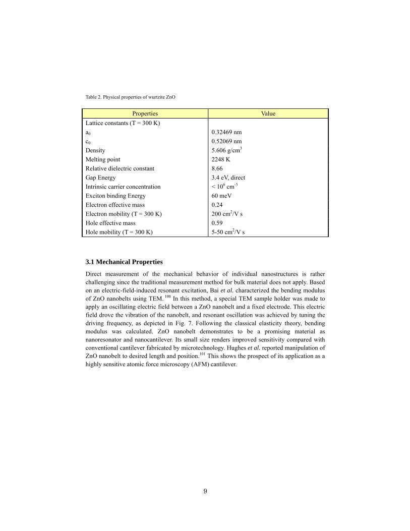
Although the vapor transport process is the dominant synthesis method for growing semiconducting nanostructures such as ZnO, GaN and Si nanowires, other growth methods such as electrodeposition, sol-gel, polymer assisted growth, etc. have been developed in parallel.85,86-92 These methods provide the possibility of forming ZnO nanostructures at low temperature. For example, in an electrodeposition method,85 AAM with highly ordered nanopores was used as a template, zinc nanowires were fabricated into the nanopores via electrodeposition, forming zinc nanowires array, then the nanowire array was oxidized at 300 °C for 2 hours and ZnO nanowire array was obtained. In a sol-gel synthesis method,86 AAM was also used as the template and immersed into a suspension containing zinc acetate for 1 minute, then heated in air at 120 °C for 6 hours. ZnO nanofibers were eventually obtained after removing the AAM template. This sol-gel process was further improved by an electrochemical method in order to obtain nanorods with diameter smaller than 50 nm.87 These methods are complementary to the vapor transport synthesis of ZnO nanostructure, and also employ less rigorous synthesis conditions and provide great potential for device applications. 3. Physical Properties of ZnO Nanostructures Table 2 lists the basic physical properties of bulk ZnO.93 It is worth noting that as the dimension of the semiconductor materials continuously shrinks down to nanometer or even smaller scale, some of their physical properties undergo changes known as the “quantum size effects”. For example, quantum confinement increases the band gap energy of quasi-one-dimensional (Q1D) ZnO, which has been confirmed by photoluminescence.94 Bandgap of ZnO nanoparticles also demonstrates such size dependence.95 X-ray absorption spectroscopy and scanning photoelectron microscopy reveal the enhancement of surface states with the downsizing of ZnO nanorods.96 In addition, the carrier concentration in Q1D systems can be significantly affected by the surface states, as suggested from nanowire chemical sensing studies.72,97-99 Understanding the fundamental physical properties is crucial to the rational design of functional devices. Investigation of the properties of individual ZnO nanostructures is essential for developing their potential as the building blocks for future nanoscale devices. This section will review the up-to-date research progress on the physical properties of ZnO nanostructures, including mechanical, piezoelectric, electrical, optical, magnetic and chemical sensing properties.
9
Table 2. Physical properties of wurtzite ZnO
Properties Value Lattice constants (T = 300 K) a0 0.32469 nm c0 0.52069 nm Density 5.606 g/cm3 Melting point 2248 K Relative dielectric constant 8.66 Gap Energy 3.4 eV, direct Intrinsic carrier concentration < 106 cm-3 Exciton binding Energy 60 meV Electron effective mass 0.24 Electron mobility (T = 300 K) 200 cm2/V s Hole effective mass 0.59 Hole mobility (T = 300 K) 5-50 cm2/V s
3.1 Mechanical Properties
Direct measurement of the mechanical behavior of individual nanostructures is rather challenging since the traditional measurement method for bulk material does not apply. Based on an electric-field-induced resonant excitation, Bai et al. characterized the bending modulus of ZnO nanobelts using TEM. 100 In this method, a special TEM sample holder was made to apply an oscillating electric field between a ZnO nanobelt and a fixed electrode. This electric field drove the vibration of the nanobelt, and resonant oscillation was achieved by tuning the driving frequency, as depicted in Fig. 7. Following the classical elasticity theory, bending modulus was calculated. ZnO nanobelt demonstrates to be a promising material as nanoresonator and nanocantilever. Its small size renders improved sensitivity compared with conventional cantilever fabricated by microtechnology. Hughes et al. reported manipulation of ZnO nanobelt to desired length and position.101 This shows the prospect of its application as a highly sensitive atomic force microscopy (AFM) cantilever.

10
Fig. 7 .TEM images of a ZnO nanobelt at (a) stationary (b) the first harmonic resonance in x (thickness) direction, νx= 622 KHz, (c) the first harmonic resonance in y (width) direction,νy= 691 KHz. (d) Resonance peak of a ZnO nanobelt. Reprint from ref. 100, X. D. Bai et al., Appl. Phys. Lett. 82, 4806 (2003) with permission from American Institute of Physics.
3.2 Piezoelectric effect and polar surfaces
As one of the important properties of ZnO, its piezoelectricity has been extensively studied for various applications in force sensing, acoustic wave resonator, acousto-optic modulator, etc.102-109 The origin of the piezoelectricity lies in its crystal structure, in which the oxygen atoms and zinc atoms are tetrahedrally bonded. In such a non-centrosymmetric structure, the center of positive charge and negative charge can be displaced due to external pressure induced lattice distortion (Fig. 8a). This displacement results in local dipole moments, thus a macroscopic dipole moments appears over the whole crystal. In fact, among the tetrahedrally bonded semiconductors, ZnO has the highest piezoelectric tensor which provides a large electro-mechanical coupling.103 The piezoelectric property of ZnO nanostructures was also investigated for their potential applications in nano-electromechanical systems.6,34,110 The piezoelectric coefficient of ZnO nanobelts was measured by AFM with conductive tips.110 As depicted in Fig. 8, ZnO nanobelts were deposited on a conductive substrate, then the whole substrate was coated with 5 nm thick Pd serving as top electrode on the nanobelt. After the

11
nanobelt was located by AFM, piezoresponse force microscopy was used to measure the effective piezocoefficient of the (0001) surface of the nanobelt. As the result, the effective piezocoefficient of nanobelt is observed to be frequency dependent and much larger than that of the bulk (0001) surface (Fig. 8b).
Fig. 8. (a) Schematics showing the piezoelectric effect in a tetrahedrally coordinated cation-anion unit. (b) Measured piezoelectric coefficient, d33, for ZnO nanobelt and its comparison with that of bulk. Reprint from ref. 6, Z. L. Wang et al., Adv. Funct. Mater. 14, 943 (2004) with permission from Wiley-VCH Verlag GMBH & Co.. (c) Schematic of using AFM to measure the ZnO nanobelt piezoelectric coefficient. Reprint from ref. 110, M. H. Zhao et al., Nano Lett. 4, 587 (2004) with permission from American Chemical Society.
Another interesting result of the non-centrosymmetric ZnO crystal structure is its
spontaneous polarization and polar face dominated nanostructures.6,34,111,112 As mentioned before, the crystal structure of ZnO can be visualized in a way that oxygen atoms and zinc atoms are tetrahedrally bonded. These tetrahedrons stack along [0001] direction. Due to spontaneous polarization, the position of positive charge is displaced from that of negative charge and the direction of displacement is also [0001]. The net result of this spontaneous polarization is a charged (0001) ZnO surface. In order to achieve minimized energy, the charged (0001) surface results in unique nano-ring and nano-coil structure, as shown in Fig. 9.
(c)
(a) (b)

12
Fig. 9. (a) Model of a polar nanobelt with top and bottome surface ±(0001) planes. Long range electrostatic force between the polar surfaces induces formation of b) nanorings, c) nanospiral, and d) nanohelixes of ZnO. The bottom graph of b,c and d are SEM images of these nanorings, nanospiral and nanohelixes. Reprint from ref. 6, Z. L. Wang et al., Adv. Funct. Mater. 14, 943 (2004) with permission from Wiley-VCH Verlag GMBH & Co..
3.3 Electrical Properties
The fundamental study of the electrical properties of ZnO nanostructures is crucial for developing their future applications in nanoelectronics. Electrical transport measurements have been performed on individual ZnO nanowires and nanorods.35,72,113-117 Single ZnO nanowire was configured as field effect transistor (FET) following several procedures.72 They were first dispersed in isopropanol alcohol to form nanowire suspension, then deposited onto a SiO2/Si substrate. Photolithography was utilized to define contact electrode array and degenerately doped Si substrate functioned as a back gate electrode. The schematic of the structure of a fabricated nanowire FET combined with the measurement circuit is depicted in Fig. 10a. Due to the native defects such as oxygen vacancies and zinc interstitials, ZnO nanowires are reported to show n-type semiconductor behavior. Fig.10b shows I-V characteristics under different back gate voltages. Well defined transfer characteristics are shown in Fig. 10c and carrier concentration and mobility are estimated. Furthermore, the electrical properties of ZnO nanowire FETs were studied using conductive AFM,118 the local electrical potential was mapped and the uniformity of nanowire electrical property was demonstrated. Furthermore, a scanning tip was capable to switch on and off the conductance periodically (Fig. 10d), indicating the potential application for a nano-electro-mechanical system.
The CVD grown ZnO nanostructures are single crystalline, rendering them superior

13
electrical property than polycrystalline thin film. For example, an electron field effect mobility of 7 cm2/V·s is regarded quite high for ZnO thin film transistors.12 However, single crystalline ZnO nanowires show mobility as high as 80 cm2/V·s.35 And Park et al. had reported an electron mobility of 1000 cm2/Vs after coating the nanowires with polyimide to reduce the electron scattering and trapping at surface.117 These results indicate that the ZnO nanostructure based device can achieve a faster operation speed than their thin film counterpart. Furthermore, using a uniquely designed synthesis setup, one can tune the carrier concentration and mobility of the nanowires (Fig. 10c), providing a way to modify the electrical property.35
The major impediment of ZnO for wide-ranging applications in electronics and photonics rests with the difficulty of p-type doping. Several p-type doping efforts have been reported, with a Ga and N codoping method, low resistivity (0.5 Ω·cm) p-type ZnO thin film was obtained.119 Look et al. reported nitrogen-doped p-type ZnO obtained by molecular beam epitaxy with a hole mobility of 2 cm2/V·s.120 Kim et al. reported phosphorus-doped p-type ZnO with a thermal activation process.121 Successful p-type doping for ZnO nanostructures will greatly enhance their future applications in nanoscale electronics and optoelectronics. P-type and n-type ZnO nanowires can serve as p-n junction diodes and light emitting diodes (LED). And field effect transistors (FET) fabricated from them can constitute complementary logic circuits. Combined with their optical cavity effect, electrically driven nanowire laser can be potentially implemented. An effort to fabricate intramolecular p-n junction on ZnO nanowires was made by Liu et al.113 In this case, anodic aluminum membrane was used as a porous template with average pore size around 40 nm. A two step vapor transport growth was applied and boron was introduced as the p-type dopant. Consequently, the I-V characteristics demonstrated rectifying behavior due to the p-n junction within the nanowire.
-4 -2 0 2 4-1600
-1200
-800
-400
0
400
Vds (V)
Vg= 6 V Vg= 4 V Vg= 2 V Vg= 0 V Vg=-2 V Vg=-4 V Vg=-6 V
I (nA
)
(b) (a)
-20 -10 0 10 20
0
50
100
150
200
B
A
Vg (V)
I (nA
)
(c)
0.0 0.5 1.0 1.5 2.002468
101214
Time (s)
I (nA
)
Vtg
Vds
(d)
14
Fig. 10. (a) AFM image of a ZnO nanowire FET combined with the schematic of the measurement circuit. (b)I-V curves of a ZnO nanowire FET from Vg = -6V to 6V; (c) Change of the transfer characteristics of two nanowires grown in different synthesis conditions. Nanowire A has a mobility of 80 cm2/V·s and carrier concentration ~106 cm-1; and nanowire B has a mobility of 22 cm2/V·s and carrier concentration ~107 cm-1. (d) A demonstration of periodic modulation of the nanowire conductance by a scanning probe. The inset is a schematic of the measurement set up.
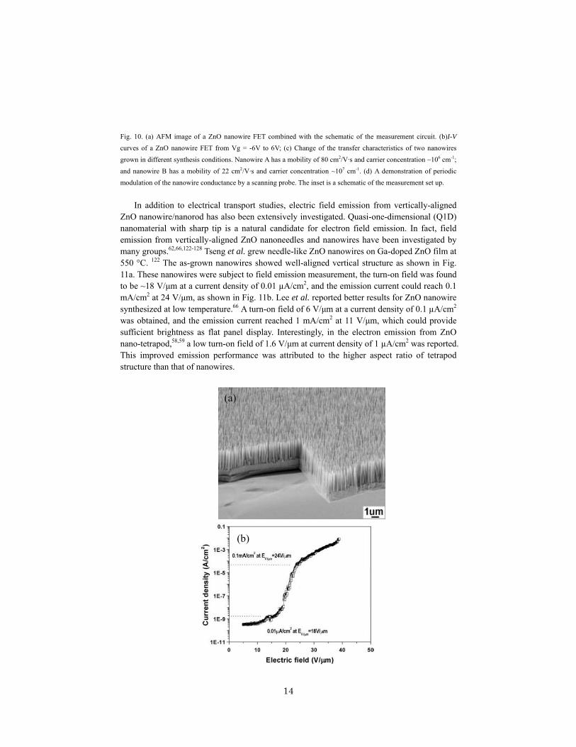
In addition to electrical transport studies, electric field emission from vertically-aligned ZnO nanowire/nanorod has also been extensively investigated. Quasi-one-dimensional (Q1D) nanomaterial with sharp tip is a natural candidate for electron field emission. In fact, field emission from vertically-aligned ZnO nanoneedles and nanowires have been investigated by many groups.62,66,122-128 Tseng et al. grew needle-like ZnO nanowires on Ga-doped ZnO film at 550 °C. 122 The as-grown nanowires showed well-aligned vertical structure as shown in Fig. 11a. These nanowires were subject to field emission measurement, the turn-on field was found to be ~18 V/µm at a current density of 0.01 µA/cm2, and the emission current could reach 0.1 mA/cm2 at 24 V/µm, as shown in Fig. 11b. Lee et al. reported better results for ZnO nanowire synthesized at low temperature.66 A turn-on field of 6 V/µm at a current density of 0.1 µA/cm2 was obtained, and the emission current reached 1 mA/cm2 at 11 V/µm, which could provide sufficient brightness as flat panel display. Interestingly, in the electron emission from ZnO nano-tetrapod,58,59 a low turn-on field of 1.6 V/µm at current density of 1 µA/cm2 was reported. This improved emission performance was attributed to the higher aspect ratio of tetrapod structure than that of nanowires.
(a)
(b)

15
Fig. 11. (a) Vertically-aligned ZnO nanowires on Ga-doped ZnO film; (b) Emission I-V characteristics of ZnO
nanowires. Reprint from ref. 122, Y.-K. Tseng et al., Adv. Funct. Mater. 13, 811 (2003) with permission from
Wiley-VCH Verlag GMBH & Co..
3.4 Optical Properties
Intrinsic optical properties of ZnO nanostructures are being intensively studied for implementing photonic devices. Photoluminescence (PL) spectra of ZnO nanostructures have been extensively reported.14,112,129-138 Excitonic emissions have been observed from the photoluminescence spectra of ZnO nanorods.139 It is shown that quantum size confinement can significantly enhance the exciton binding energy.140 Strong emission peak at 380 nm due to band-to-band transition and green-yellow emission band related to oxygen vacancy are observed. These results are consistent with those of bulk ZnO. Interestingly, the green emission intensity increases with decreasing nanowires diameter. This observation is attributed to the larger surface-to-volume ratio of thinner nanowires favoring a higher level of defects and surface recombination.14,141 Recently, red luminescence band was reported, which was attributed to doubly ionized oxygen vacancies.142 In addition, as one of the characteristics of nanoscale systems, quantum confinement was observed to cause a blue shift in the near UV emission peak in ZnO nanobelts.94 as illustrated in Fig. 12a. PL spectra show that ZnO nanowire is a promising material for UV emission, while its UV lasing property is of more significance and interest. Due to its near-cylindrical geometry and large refractive index (~2.0), ZnO nanowire/nanorod is a natural candidate for optical waveguide. The well-facetted nanowires also form promising optical resonance cavities which greatly facilitate highly directional lasing at room temperature in well aligned ZnO nanowires.14,79 Huang et al. and Liu et al. reported room temperature UV lasing from ordered ZnO nanowires array.77,78 Lasing power threshold of 40 kW/cm2 ~ 100 kW/cm2 was reported and it was suggested that higher crystal quality confers lower threshold. The additional advantages of ZnO nanowire lasers are that the excitonic recombination lowers the threshold of lasing, and quantum confinement yields a substantial density of states at the band edges and enhances radiative efficiency. Optical waveguiding using dielectric nanowire also achieved considerable progress. Recently, ZnO nanowires were reported as sub-wavelength optical waveguide.143 Optically pumped light emission was guided by ZnO nanowire and coupled into SnO2 nanoribbon (Fig. 12b,c). These findings show that ZnO nanostructures can be potential building blocks for integrated optoelectronic circuits.
Besides UV emitting and lasing, effort on utilizing ZnO nanowires for UV photodetection and optical switching have been reported by Kind et al.144 Defect state related visible wavelength detection and polarized photodetection of ZnO nanowires were also observed (Fig. 12d).142 Photocurrent is maximized when the electric field component of the incident light is polarized parallel to the nanowire long axis. This behavior is one of the characteristics of Q1D systems and renders them promising application in high contrast polarizer. From the photoconductivity measurements of ZnO nanowires, it is found that the presence of O2 has an

16
important effect on the photoresponse,115,142,145 i.e. O2 surface adsorption on the nanowires could significantly expedite the photocurrent relaxation rate. As shown in Fig. 12e, the photocurrent relaxation time is around 8 s in air but hours in vacuum. It was found that the desportion-adsorption process of O2 affects the photoresponse of ZnO nanowire. Upon illumination, photogenerated holes discharge surface chemisorbed O2 through surface electron-hole recombination, while the photogenerated electrons significantly increase the conductivity. When illumination is switched off, O2 molecules re-adsorb onto nanowire surface and reduce the conductivity. Fig. 12. (a) PL spectra of 6 and 200 nm wide ZnO nanobelts show a blue shift of the emission peak. Reprint from ref. 94, X. Wang et al., J. Phys. Chem. B 108, 8773 (2004) with permission from American Chemical Society. (b) A PL image of a ZnO nanowire guiding light into a SnO2 nanoribbon and (c) a SEM image of the wire-ribbon junction. Reprint from ref. 143, M. Law et al., Science 305, 1269 (2004) with permission from American Association for the Advancement of Science. (d) Polarized photodetection of both UV (365 nm) and visible light show that nanowire conductance is maximized when incident light is polarized parallel to the nanowire axis. (e) Nanowire photoresponse to 633 nm laser in air compared to that in vacuum (inset). Reprint from ref. 142, Z. Fan et al., Appl. Phys. Lett. 85, 6128 (2004) with permission from American Institute of Physics.
(a)
0 50 100 150 200
4
8
12
16
20
24
28
0 20 40 60 800
20
40
60
80
Turn on laser
Cur
rent
(nA
)
Time (min)
Turn off laser
Vds=0.25V
Vds=0.25V
Cur
rent
(nA
)
Time (s)
With 633 nm
(e)
0 30 60 90 120 150 180
600
800
1000
1200
1400
1600
With 365 nm UV
Vds= 2 V
Vds= 5 V
Polarization Angle (degree)
Cur
rent
(nA)
E NW
NWE
With halogen light
(d)
Z n O / S n O 2
j u n c t i o n
Z n On a n o w i r e
S n O 2
n a n o w i r e
(b) (c)

17
3.5 Magnetic Doping
Dilute magnetic semiconductors (DMS) are attracting increasing research interests because spin-polarized DMS can accomplish efficient spin injection as well as overcome the conductance mismatch associated with semiconductor devices. It has been found that ZnO is a promising host material for ferromagnetic doping. Room temperature hole mediated ferromagnetic ordering in ZnO by introducing manganese (Mn) as dopant has been predicted theoretically20,146 and reported experimentally by Sharma et al. in ZnO thin film.21 Ferromagnetism in ZnO was also observed when Co 147,148 and Fe 149,150 were used as dopants. The effort of growing ferromagnetic Zn1-xMnxO (x=0.13) nanowires with Curie temperature of 37 K was reported by Chang et al. 151 and shown in Fig. 13. The nanowires were synthesized via a vapor phase evaporation method. Because of its wide band gap, ferromagnetic ZnO is regarded as an excellent material for short wavelength magneto-optical devices.152 These studies enable the use of magnetic ZnO nanowires as nanoscale spin-based devices.153 Fig. 13. Temperature dependent magnetization curve of Zn1-xMnxO (x=0.13) nanowire at 500 Oe field shows Curie temperature of 37K. Inset: Magnetization-Field hysteresis loop obtained at 5 K demonstrates ferromagnetism by Mn doping. Reprint from ref. 151, Y. Q. Chang et al., Appl. Phys. Lett. 83 4020 (2003) with permission from American Institute of Physics.
3.6 Chemical Sensing
Oxygen vacancies on metal-oxide surfaces are electrically and chemically active. These vacancies function as n-type donors, often significantly increase the conductivity of oxide. Upon adsorption of charge accepting molecules at the vacancy sites, such as NO2 and O2, electrons are effectively depleted from the conduction band, leading to a reduced conductivity of the n-type oxide. On the other hand, molecules, such as CO and H2, would react with surface adsorbed oxygen and consequently remove it, leading to an increase of conductivity. Most metal-oxide gas sensors operate based on this principle. As one of the major materials for solid state gas sensor, bulk and thin films of ZnO have been proposed for CO 16, NH3 17, alcohol 18 and H2 19 sensing under elevated temperature (~400 °C). From the aspect of sensing performance, Q1D ZnO, such as nanowires and nanorods, is expected to be superior to its thin
18
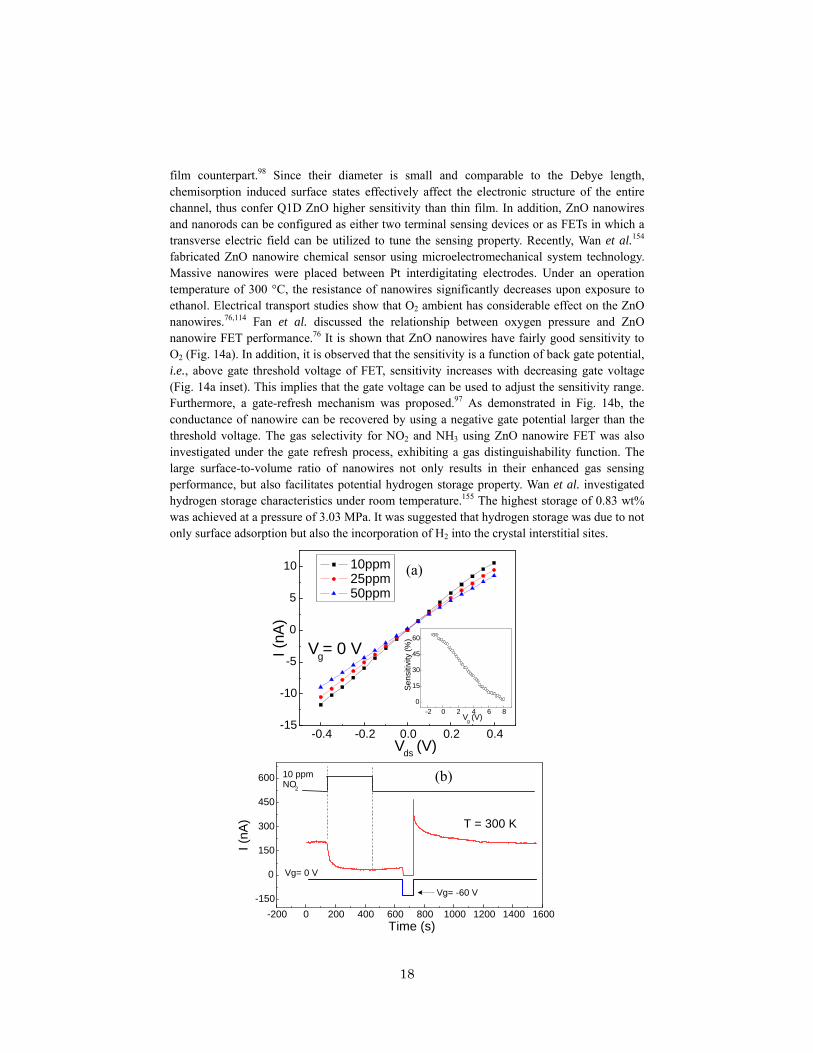
film counterpart.98 Since their diameter is small and comparable to the Debye length, chemisorption induced surface states effectively affect the electronic structure of the entire channel, thus confer Q1D ZnO higher sensitivity than thin film. In addition, ZnO nanowires and nanorods can be configured as either two terminal sensing devices or as FETs in which a transverse electric field can be utilized to tune the sensing property. Recently, Wan et al.154 fabricated ZnO nanowire chemical sensor using microelectromechanical system technology. Massive nanowires were placed between Pt interdigitating electrodes. Under an operation temperature of 300 °C, the resistance of nanowires significantly decreases upon exposure to ethanol. Electrical transport studies show that O2 ambient has considerable effect on the ZnO nanowires.76,114 Fan et al. discussed the relationship between oxygen pressure and ZnO nanowire FET performance.76 It is shown that ZnO nanowires have fairly good sensitivity to O2 (Fig. 14a). In addition, it is observed that the sensitivity is a function of back gate potential, i.e., above gate threshold voltage of FET, sensitivity increases with decreasing gate voltage (Fig. 14a inset). This implies that the gate voltage can be used to adjust the sensitivity range. Furthermore, a gate-refresh mechanism was proposed.97 As demonstrated in Fig. 14b, the conductance of nanowire can be recovered by using a negative gate potential larger than the threshold voltage. The gas selectivity for NO2 and NH3 using ZnO nanowire FET was also investigated under the gate refresh process, exhibiting a gas distinguishability function. The large surface-to-volume ratio of nanowires not only results in their enhanced gas sensing performance, but also facilitates potential hydrogen storage property. Wan et al. investigated hydrogen storage characteristics under room temperature.155 The highest storage of 0.83 wt% was achieved at a pressure of 3.03 MPa. It was suggested that hydrogen storage was due to not only surface adsorption but also the incorporation of H2 into the crystal interstitial sites.
-0.4 -0.2 0.0 0.2 0.4-15
-10
-5
0
5
10
Vg= 0 VI (nA
)
Vds (V)
-2 0 2 4 6 80
15
30
45
60
Vg (V)
Sens
itivi
ty (%
)
10ppm25ppm50ppm
(a)
-200 0 200 400 600 800 1000 1200 1400 1600-150
0
150
300
450
600 10 ppmNO2
I (nA
)
Time (s)
Vg= -60 V
Vg= 0 V
T = 300 K
(b)

19
Fig. 14. (a) I-V curves of a ZnO nanowire under 50 ppm O2. Inset: gate potential dependence of sensitivity under 10 ppm O2. Reprint from ref. 76, Z. Fan et al., Appl. Phys. Lett. 85,5923 (2004) with permission from American Institute of Physics. (b) The nanowire sensing response to 10 ppm NO2 and the conductance recovery process assisted by a -60 V gate voltage pulse. Reprint from ref. 97, Z. Fan et al., Appl. Phys. Lett. 86, 123510 (2005) with permission from American Institute of Physics. 4. Conclusions ZnO offers tremendous potential in future applications of electronic, optoelectronic, and magnetoelectronic devices. Encouraging progress on the research of nanostructured ZnO materials have been accomplished as reviewed in this article. There are still important issues waiting to be further investigated. One key area is the growth of p-type ZnO nanowires and fabrication of nanoscale p-n junctions for electrically driven nano LED or laser. Integration of ZnO nanostructure building blocks for large scale device applications is another important issue. Continuous effort is dedicated to achieve large arrays of programmable structures for building reconfigurable architectures. Last but not the least, obtaining room temperature ferromagnetism and demonstrating spin-polarized transport in ZnO nanostructures will greatly advance future research on spin-based nanoscale devices. Acknowledgement This work is supported by National Science Foundation. The authors thank Mr. P.-C. Chang for helpful discussions.

20
References
1. K. Nomura, H. Ohta, K. Ueda, T. Kamiya, M. Hirano, and H. Hosono, Science 300, 1269
(2003). 2. T. Nakada, Y. Hirabayashi, T. Tokado, D. Ohmori, and T. Mise, Sol. Energy 77, 739
(2004). 3. S. Y. Lee, E. S. Shim, H. S. Kang, S. S. Pang, and J. S. Kang, Thin Solid Films 437, 31
(2005). 4. R. Könenkamp, R. C. Word, and C. Schlegel, Appl. Phys. Lett. 85, 6004 (2004). 5. S. T. Mckinstry, and P. Muralt, J. Electroceram. 12, 7 (2004). 6. Z. L. Wang, X. Y. Kong, Y. Ding, P. Gao, W. L. Hughes, R. Yang, and Y. Zhang, Adv.
Funct. Mater. 14, 943 (2004). 7. M. S. Wagh, L. A. Patil, T. Seth, and D. P. Amalnerkar, Mater. Chem. Phys. 84, 228
(2004). 8. Y. Ushio, M. Miyayama, and H. Yanagida, Sensor Actuat. B 17, 221 (1994). 9. H. Harima, J. Phys.: Condens. Matter 16, S5653 (2004). 10. S. J. Pearton, W. H. Heo, M. Ivill, D. P. Norton, and T. Steiner, Semicond. Sci. Technol.
19, R59 (2004). 11. J. Nishii, F.M. Hossain, S. Takagi, T. Aita, K. Saikusa, Y. Ohmaki, I. Ohkubo, S.
Kishimoto, A. Ohtomo, T. Fukumura, F. Matsukura, Y. Ohno, H. Koinuma, H. Ohno, and M. Kawasaki, Jpn. J. Appl. Phys. 42, L347 (2003).
12. F. M. Hossain, J. Nishii, S. Takagi, T. Sugihara, A. Ohtomo, T. Fukumura, H. Koinuma, H. Ohno, M. Kawasaki, Physica E 21, 911 (2004).
13. B.J. Norris, J. Anderson, J.F. Wager, D.A. Kszler, J. Phys. D: Appl. Phys. 36, L105 (2003).
14. P. Yang, H. Yan, S. Mao, R. Russo, J. Johnson, R. Saykally, N. Morris, J. Pham, R. He, H.-J. Choi, Adv. Mater. 12, 323 (2002).
15. Y. Ito, K. Kushida, K. Sugawara, and H. Takeuchi, IEEE Trans. Ultrasonics, Ferroelectrics, and Frequency Control 42, 316 (1995).
16. H.-W. Ryu, B.-S. Park, S. A. Akbar, W.-S. Lee, K.-J. Hong, Y.-Jin Seo, D.-C. Shin, J.-S. Park, G.-P. Choi, Sens. Actuator B 96, 717 (2003).
17. G. Sberveglieri, Sens. Actuator B 23, 103 (1995). 18. G. S. Trivikrama Rao, D. Tarakarama Rao, Sens. Actuator B 55, 166 (1999). 19. X. L. Cheng, H. Zhao, L. H. Huo, S. Gao, J. G. Zhao, Sens. Actuator B 102, 248 (2004). 20. T. Dietl, Semicond. Sci. Technol. 17, 377 (2002). 21. P. Sharma, A. Gupta, K. V. Rao, F. J. Owens, R. Sharma, R. Ahuja, J. M. Osorio, B.
Johansson, G. A. Gehring, Nat. Mater. 2, 673 (2003). 22. H. Saeki, H. Tabata, T. Kawai, Solid State Commun. 120, 439 (2001). 23. S. Fujita, S.-W. Kim, M. Ueda, and S. Fujita, J. Cryst. Growth 272, 138 (2004). 24. H. Zhou, and Z. Li, Mater. Chem. Phys. 89, 326 (2005). 25. D. W. Zeng, C. S. Xie, M. Dong, R. Jiang, X. Chen, A. H. Wang, J. B. Wang, and J. Shi,
Appl. Phys. A 79, 1865 (2004).

21
26. J. Zhang, L.-D. Sun, X.-C. Jiang, C.-S. Lian, and C.-H. Yan, Cryst. Growth Des. 4, 309 (2004).
27. H. Zhang, D. Yang, X. Ma, Y. Ji, J. Xu, and D. Que, Nanotechnology 15, 622 (2004). 28. P. X. Gao, and Z. L. Wang, J. Phys. Chem. B 108, 7534 (2004). 29. Y. H. Leung, A. B. Djurišić, J. Gao, M. H. Xie, Z. F. Wei, S. J. Xu, and W. K. Chan,
Chem. Phys. Lett. 394, 452 (2004). 30. F. Liu, P. J. Cao, H. R. Zhang, J. Q. Li, and H. J. Gao, Nanotechnology 15, 949 (2004). 31. P.-A. Hu, Y.-Q. Liu, L. Fu, X.-B. Wang, D.-B. Zhu, Appl. Phys. A 78, 15 (2004). 32. Z. R. Tian, J. A. Voigt, J. Liu, B. Mckenzie, M. J. Mcdermott, Nat. Mater. 2, 821 (2003). 33. Z. Fan, and J. G. Lu, International Journal of High Speed Electronics and Systems, to be
published. 34. X. Y. Kong, Z. L. Wang, Nano. Lett. 3, 1625 (2003). 35. P. Chang, Z. Fan, W. Tseng, D. Wang, W. Chiou, J. Hong, J. G. Lu, Chem. Mater. 16,
5133 (2004). 36. H. Y. Dang, J. Wang, and S. S. Fan, Nanotechnology 14, 738 (2003). 37. W. I. Park, and G.-C. Yi, Adv. Mater. 16, 87 (2004). 38. S. J. An, W. I. Park, G.-C. Yi, Y.-J. Kim, H.-B. Kang, and M. Kim, Appl. Phys. Lett. 84,
3612 (2004). 39. W. Lee, M.-C. Jeong, and J.-M. Myoung, Acta Mater. 52, 3949 (2004). 40. B. P. Zhang, N. T. Binh, K. Wakatsuki, Y. Segawa, Y. Kashiwaba, and K. Haga,
Nanotechnology 15, S382 (2004). 41. H.-J. Kim, K. Sung, K.-S. An, Y. K. Lee, C. G. Kim, Y.-H. Lee, and Y. Kim, J. Mater.
Chem. 14, 3306 (2004). 42. M. H. Huang, Y. Wu, H. Feick, N. Tran, E. Weber, and P. Yang, Adv. Mater. 13, 113
(2001). 43. S. Y. Li, C. Y. Lee, T. Y. Tseng, J. Cryst. Growth 247, 357 (2003). 44. X. Kong, X. Sun, X. Li, and Y. Li, Mater. Chem. Phys. 82, 997 (2003). 45. W. D. Yu, X. M. Li, and X. D. Gao, Appl. Phys. Lett. 84, 2658 (2004). 46. W. D. Yu, X. M. Li, X. D. Gao, P. S. Qiu, W. X. Cheng, and A. L. Ding, Appl. Phys. A 79,
453 (2004). 47. H. T. Ng, J. Han, T. Yamada, P. Nguyen, Y. P. Chen, M. Meyyappan, Nano. Lett. 4, 1247
(2004). 48. X. Wang, C.J. Summers, and Z.L. Wang, Nano Lett. 4, 423 (2004). 49. P. X. Gao, Y. Ding, and Z. L. Wang, Nano Lett. 3, 1315 (2003). 50. J. Y. Lao, J. G. Wen, Z. F. Ren, Nano. Lett. 2, 1287 (2002). 51. J. G. Wen, J. Y. Lao, D. Z. Wang, T. M. Kyaw, Y. L. Foo, and Z. F. Ren, Chem. Phys. Lett.
372, 717 (2003). 52. B. D. Yao, Y. F. Chan, N. Wang, Appl. Phys. Lett. 81, 757 (2002). 53. R. M. Wang, Y. J. Xing, J. Xu, and D. P. Yu, New J. Phys. 5, 115.1 (2003). 54. X.-H. Zhang, S.-Y. Xie, Z.-Y. Jiang, X. Zhang, Z.-Q. Tian, Z.-X. Xie, R.-B. Huang, and
L.-S. Zheng, J. Phys. Chem. B 107, 10114 (2003). 55. Y. Dai, Y. Zhang, and Z. L. Wang, Solid State Commun. 126, 629 (2003). 56. Y. H. Leung, A. B. Djurišić, J. Gao, M. H. Xie, Z. F. Wei, S. J. Xu, and W. K. Chan,
Chem. Phys. Lett. 385, 155 (2004).

22
57. F. Z. Wang, Z. Z. Ye, D. W. Ma, L. P. Zhu, and F. Zhuge, Mater. Lett. 59, 560 (2005). 58. Q. Wan, K. Yu, T. H. Wang, and C. L. Lin, Appl. Phys. Lett. 83, 2253 (2003). 59. Q. H. Li, Q. Wan, Y. J. Chen, T. H. Wang, H. B. Jia, and D. P. Yu, Appl. Phys. Lett. 85,
636 (2004). 60. H. J. Fan, F. Bertram, A. Dadgar, J. Christen, A. Krost, and M. Zacharias,
Nanotechnology 15, 1401 (2004). 61. Y.-K. Tseng, C.-T. Chia, C.-Y. Tsay, L.-J. Lin, H.-M. Cheng, C.-Y. Kwo, and I.-C. Chen,
J. Electrochem. Soc. 152, G95 (2005). 62. D. Banerjee, S. H. Jo, and Z. F. Ren, Adv. Mater. 16, 2028 (2004). 63. J. Y. Lao, J. Y. Huang, D. Z. Wang, and Z. F. Ren, J. Mater. Chem. 14, 770 (2004). 64. S. Y. Bae, H. W. Seo, H. C. Choi, J. Park, and J. Park, J. Phys. Chem. B 108, 12318
(2004). 65. M. Guo, P. Diao, S. M. Cai, Chinese Chem. Lett. 15, 1113 (2004). 66. Y. J. Xing, Z. H. Xi, Z. Q. Xue, X. D. Zhang, J. H. Song, R. M. Wang, J. Xu, Y. Song, S.
L. Zhang, D. P. Yu, Appl. Phys. Lett. 83, 1689 (2003). 67. X.-H. Zhang, S.-Y. Xie, Z.-Y. Jing, Z.-X. Xie, R.-B. Huang, L.-S. Zheng, J.-Y. Kang, T.
Sekiguchi, J. Solid State Chem. 173, 109 (2003). 68. R. K. Zheng, H. Liu, X. X. Zhang, V. A. L. Roy, A. B. Djurišić, Appl. Phys. Lett. 85,
2589 (2004). 69. Q. X. Zhao, M. Millander, R. E. Morjan, Q.-H. Hu, E. E. B. Campbell, Appl. Phys. Lett.
83, 165 (2003). 70. C. J. Lee, T. J. Lee, S. C. Lyu, Y. Zhang, H. Ruh, H. J. Lee, Appl. Phys. Lett. 81, 3648
(2002). 71. S. Y. Li, P. Lin, C. Y. Lee, M. S. Ho, T. Y. Tseng, J. Nanosci. Nanotech. 4, 968 (2004). 72. H. Chik, J. Liang, S. G. Cloutier, N. Kouklin, J. M. Xu, Appl. Phys. Lett. 84, 3376
(2004). 73. E. C. Greyson, Y. Babayan, and T. W. Odom, Adv. Mater. 16, 1348 (2004). 74. H. J. Fan, F. Fleischer, W. Lee, K. Nielsch, R. Scholz, M. Zacharias, U. Gösele, A.
Dadgar, and A. Krost, Supperlattice Microst. 36, 95 (2004). 75. Y. Ding, P. X. Gao, and Z. L. Wang, J. Am. Chem. Soc. 126, 2066 (2004). 76. Z. Fan, D. Wang, P. Chang, W. Tseng, J. G. Lu, Appl. Phys. Lett. 85, 5923 (2004). 77. M. H. Huang, S. Mao, H. Feick, H. Yan, Y. Wu, H. Kind, E. Weber, R. Russo, P. Yang,
Science 292, 1897 (2001). 78. C. Liu, J. A. Zapien, Y. Yao, X. Meng, C. S. Lee, S. Fan, Y. Lifshitz, S. T. Lee, Adv.
Mater. 15, 838 (2003). 79. J. C. Johnson, H. Yan, P. Yang, R. J. Saykalley, J. Phys. Chem. B 107, 8816 (2003). 80. M. Yan, H. T. Zhang, E. J. Widjaja, and R. P. H. Chang, J. Appl. Phys. 94, 5240 (2003). 81. C. Geng, Y. Jiang, Y. Yao, X. Meng, J. A. Zapien, C. S. Lee, Y. Lifshitz, and S. T. Lee,
Adv. Funct. Mater. 14, 589 (2004). 82. Y. Zhang, H. Jia, R. Wang, C. Chen, X. Luo, D. Yu, and C. Lee, Appl. Phys. Lett. 83,
4631 (2003). 83. J.-J. Wu, and S.-C. Liu, Adv. Mater. 14, 215 (2002). 84. J. Park, H.-Ho Choi, K. Siebein, and R. K. Singh, J. Cryst. Growth 258, 342 (2003). 85. Y. Li, G. S. Cheng, and L. D. Zhang, J. Mater. Res. 15, 2305 (2000).

23
86. B. B. Lakshmi, P. K. Dorhout, and C. R. Martin, Chem. Mater. 9, 857 (1997). 87. Z. Miao, D. Xu, J. Ouyang, G. Guo, X. Zhao, and Y. Tang, Nano Lett. 2, 717 (2002). 88. Z. Li, Y. Xiong, and Y. Xie, Inorg. Chem. 42, 8105 (2003). 89. H. Zhang, D. Yang, Y. Ji, X. Ma, J. Xu, and D. Que, J. Phys. Chem. B 108, 3955 (2004). 90. B. Liu, and H. C. Zeng, Langmuir 20, 4196 (2004). 91. R. F. Mulligan, A. A. Iliadis, and P. Kofina, J. Appl. Polym. Sci. 89, 1058 (2003). 92. B. Cheng, and E. T. Samulski, Chem. Commun. 8, 986 (2004). 93. S. J. Pearton, D. P. Norton, K. Ip, Y. W. Heo, T. Steiner, Prog. Mater. Sci. 50, 293 (2005). 94. X. Wang, Y. Ding, C. J. Summers, Z. L. Wang, J. Phys. Chem. B 108, 8773 (2004). 95. L. M. Kukreja, S. Barik, P. Misra, J. Cryst. Growth 268, 531 (2004). 96. J. W. Chiou, K. P. Krishna Kumar, J. C. Jan, H. M. Tsai, C. W. Bao, W. F. Pong, F. Z.
Chien, M.-H. Tsai, I.-H. Hong, R. Klauser, J. F. Lee, J. J. Wu, and S. C. Liu, Appl. Phys. Lett. 85, 3220 (2004).
97. Z. Fan, and J. G. Lu, Appl. Phys. Lett. 86, 123510 (2005). 98. A. Kolmakov, and M. Moskovits, Annu. Rev. Mater. Res. 34, 151 (2004). 99. Y. Zhang, A. Kolmakov, S. Chretien, H. Metiu, M. Moskovits, Nano Lett. 4, 403 (2004). 100. X. D. Bai, P. X. Gao, Z. L. Wang, E. G. Wang, Appl. Phys. Lett. 82, 4806 (2003). 101. W. L. Hughes, Z. L. Wang, Appl. Phys. Lett. 82, 2886 (2003). 102. M. Catti, Y. Noel, and R. Dovesi, J. Phys. Chem. Solids 64, 2183 (2003). 103. A. D. Corso, M. Posternak, R. Resta, and A. Balderschi, Phys. Rev. B 50, 10715 (1994). 104. J. G. E. Gardeniers, Z. M. Rittersma, and G. J. Burger, J. Appl. Phys. 83, 7844 (1998). 105. J. Molarius, J. Kaitila, T. Pensala, and M. Ylilammi, J. Mater. Sci.-Mater. El. 14, 431
(2003). 106. C. R. Wuethrich, C. A. P. Muller, G. R. Fox, and H. G. Limberger, Sensor Actuat. A 66,
114 (1998). 107. T. Itoh, and T. Suga, Appl. Phys. Lett. 64, 37 (1994). 108. R. Paneva, G. Temmel, E. Burte, and H. Ryssel, Sensor Actuat. A 62, 765 (1997). 109. A R. Hutson, Phys. Rev. Lett. 4, 505 (1960). 110. M. H. Zhao, Z. L. Wang, and S. X. Mao, Nano Lett. 4, 587 (2004). 111. X. Y. Kong, Y. Ding, R. Yang, and Z. L. Wang, Science 303, 1348 (2004). 112. X. Y. Kong, and Z. L. Wang, Appl. Phys. Lett. 84, 975 (2004). 113. C. H. Liu, W. C. Yiu, F. C. K. Au, J. X. Ding, C. S. Lee, S. T. Lee, Appl. Phys. Lett. 83,
3168 (2003). 114. Q. H. Li, Q. Wan, Y. X. Liang, T. H. Wang, Appl. Phys. Lett. 84, 4556 (2004). 115. Y. W. Heo, L. C. Tien, D. P. Norton, B. S. Kang, F. Ren, B. P. Gila, S. J. Pearton, Appl.
Phys. Lett. 85, 2002 (2004). 116. M. S. Arnold, P. Avouris, Z. W. Pan, Z. L. Wang, J. Phys. Chem. B 107, 659 (2003). 117. W. I. Park, J. S. Kim, G.-C. Yi, M. H. Bae, H.-J, Lee, Appl. Phys. Lett. 85, 5052 (2004). 118. Z. Fan, and J. G. Lu, Appl. Phys. Lett. 86, 03211 (2005). 119. M. Joseph, H. Tabata, H. Saeki, K. Ueda, T. Kawai, Physica B 302-303, 140 (2001). 120. D. C. Look, D. C. Reynolds, C. W. Litton, R. L. Jones, D. B. Eason, G. Cantwell, Appl.
Phys. Lett. 81, 1830 (2002). 121. K.-K. Kim, H.-S. Kim, D.-K. Hwang, J.-H. Lim, S.-J. Park, Appl. Phys. Lett. 83, 63
(2003).

24
122. Y.-K. Tseng, C.-J. Huang, H.-M. Cheng, I.-N. Lin, K.-S. Liu, I.-C. Chen, Adv. Funct. Mater. 13, 811 (2003).
123. Y. W. Zhu, H. Z. Zhang, X. C. Sun, S. Q. Feng, J. Xu, Q. Zhao, B. Xiang, R. M. Wang, D. P. Yu, Appl. Phys. Lett. 83, 144 (2003).
124. H. Z. Zhang, R. M. Wang, Y. W. Zhu, J. Appl. Phys. 96, 624 (2004). 125. Y. B. Li, Y. Bando, and D. Golberg, Appl. Phys. Lett. 84, 3603 (2004). 126. C. X. Xu and X. W. Sun, Appl. Phys. Lett. 83, 3806 (2003). 127. S. H. Jo, D. Banerjee, and Z. F. Ren, Appl. Phys. Lett. 85, 1407 (2004). 128. T. Y. Kim, J. Y. Kim, S. H. Lee, H. W. Shim, S. H. Lee, E. K. Suh, and K. S. Nahm,
Sythetic Met. 144, 61 (2004). 129. H. T. Ng, B. Chen, J. Li, J. Han, M. Meyyappan, Appl. Phys. Lett. 82, 2023 (2003). 130. D. F. Liu, D. S. Tang, L. J. Ci, X. Q. Yan, Y. X. Liang, Z. P. Zhou, H. J. Yuan, W. Y. Zhou,
G. Wang, Chin. Phys. Lett. 20, 928 (2003). 131. S. C. Lyu, Y. Zhang, H. Ruh, H.-J. Lee, H.-W. Shim, E.-K. Suh, C. J. Lee, Chem. Phys.
Lett. 363, 134 (2002). 132. T.-W. Kim, T. Kawazoe, S. Yamazaki, M. Ohtsu, and T. Sekiguchi, Appl. Phys. Lett. 84,
3358 (2004). 133. S. Chakrabarti, and S. Chaudhuri, Mater. Chem. Phys. 87, 196 (2004). 134. D. Li, Y. H. Leung, A. B. Djurišić, Z. T. Liu, M. H. Xie, S. L. Shi, and S. J. Xu, Appl.
Phys. Lett. 85, 1601 (2004). 135. H. J. Fan, R. Scholz, F. M. Kolb, M. Zacharias, U. Gösele, F. Heyroth, C. Eisenschmidt,
T. Hempel, J. Christen, Appl. Phys. A 79, 1895 (2004). 136. T. Y. Kim, J. Y. Kim, M. S. Kumar, E.-K. Suh, K. S. Nahm, J. Cryt. Growth 270, 491
(2004). 137. D. Zhao, C. Andreazza, P. Andreazza, J. Ma, Y. Liu, and D. Shen, Chem. Phys. Lett. 399,
522 (2004). 138. W. Lee, M.-C. Jeong, and J.-M. Myoung, Nanotechnology 15, 1441 (2004). 139. W.I. Park, Y.H. Jun, S.W. Jung, and G. Yi, Appl. Phys. Lett. 82, 964 (2003) 140. Y. Gu, I. L. Kuskovsky, M. Yin, S. O’Brien, and G. G. Neumark, Appl. Phys. Lett. 85,
3833 (2004). 141. I. Shalish, H. Temkin, and V. Narayanamurti, Phys. Rev. B. 69, 245401 (2004). 142. Z. Fan, P. Chang, E. C. Walter, C. Lin, H. P. Lee, R. M. Penner, J. G. Lu, Appl. Phys. Lett.
85, 6128 (2004). 143. M. Law, D. J. Sirbuly, J. C. Johnson, J. Goldberger, R. J. Saykally, P. Yang, Science 305,
1269 (2004). 144. H. Kind, H. Yan, B. Messer, M. Law, P. Yang, Adv. Mater. 14, 158 (2002). 145. K. Keem, H. Kim, G.-T. Kim, J. S. Lee, B. Min, K. Cho, M.-Y. Sung, S. Kim, Appl. Phys.
Lett. 84, 4376 (2004). 146. N. A. Spaldin, Phys. Rev. B 69, 125201 (2004). 147. K. Rode, A. Anane, R. Mattana, J.-P. Contour, J. Appl. Phys. 93, 7676 (2003). 148. N. A. Theodoropoulou, A. F. Hebard, D. P. Norton, J. D. Budai, L. A. Boatner, J. S. Lee,
Z. G. Khim, Y. D. Park, M. E. Overberg, S. J. Pearton, and R. G. Wilson, Solid State Electron. 47, 2231 (2003).
149. Y. M. Cho, W. K. Choo, H. Kim, D. Kim, Y. Ihm, Appl. Phys. Lett. 80, 3358 (2002).

25
150. S.-J. Han, J. W. Song, C.-H. Yang, S. H. Park, J.-H. Park, Y. H. Jeong, K. W. Rhie, Appl. Phys. Lett. 81, pp. 4212 (2002).
151. Y. Q. Chang, D. B. Wang, X. H. Luo, X. Y. Xu, X. H. Chen, L. Li, C. P. Chen, R. M. Wang, J. Xu, D. P. Yu, Appl. Phys. Lett. 83 4020 (2003).
152. K. Ando, H. Saito, Z. Jin, T. Fukumura, M. Kawasaki, Y. Matsumoto, H. Koinuma, Appl. Phys. Lett. 78, 2700 (2001).
153. C. Ronning, P. X. Gao, Y. Ding, Z. L. Wang, and D. Schwen, Appl. Phys. Lett. 84, 783 (2004).
154. Q. Wan, Q. H. Li, Y. J. Chen, T. H. Wang, X. L. He, J. P. Li, C. L. Lin, Appl. Phys. Lett. 84, 3654 (2004).
155. Q. Wan, C. L. Lin, X. B. Xu, T. H. Wang, Appl. Phys. Lett. 84, 124 (2004).