1 graphene nanoribbons - usc department of...
TRANSCRIPT

1
GRAPHENE NANORIBBONS
USC Department of Physics Graduate Seminar
Nahid Shayesteh,

2
Carbon based material
Discovery and innovation of graphen
Graphene nanoribbons structure
Application of Graphene nanoribbons
Outlines…
Nahid Shayesteh, Department of Physics
3
Carbon-based nanoelectronics….
1. Replace silicon-based micro electronics.
2. Exhibit superior physical properties in many aspects.
3. Industrial applications
FUNCTIONS…
Nahid Shayesteh, Department of Physics

4
The term graphene
1962—Hanns-Peter Boehm coined graphene as a combination of graphite and the suffix –ene to describe single-layer carbon foils.
Hanns-Peter Boehm: Born January 9, 1928 in Paris German Chemist
Professor Emeritus in Ludwig-Maximillians University in Munich,Germany
Pioneer of graphene research
History…
Nahid Shayesteh, Department of Physics

5
Mitsutaka Fujita (藤田 光孝 Fujita Mitsutaka)
Introduced graphene nanoribbons as a theory model to examine the edge and nanoscale size effect in graphene.
Japanese Physicist
Born: August 16, 1959
Died: March 18, 1998
Innovation…
Nahid Shayesteh, Department of Physics

6
Definition: thin strips of graphene
Graphene nanoribbons
GNR’s
Nano-graphene ribbons
Terminology…
Nahid Shayesteh, Department of Physics
7
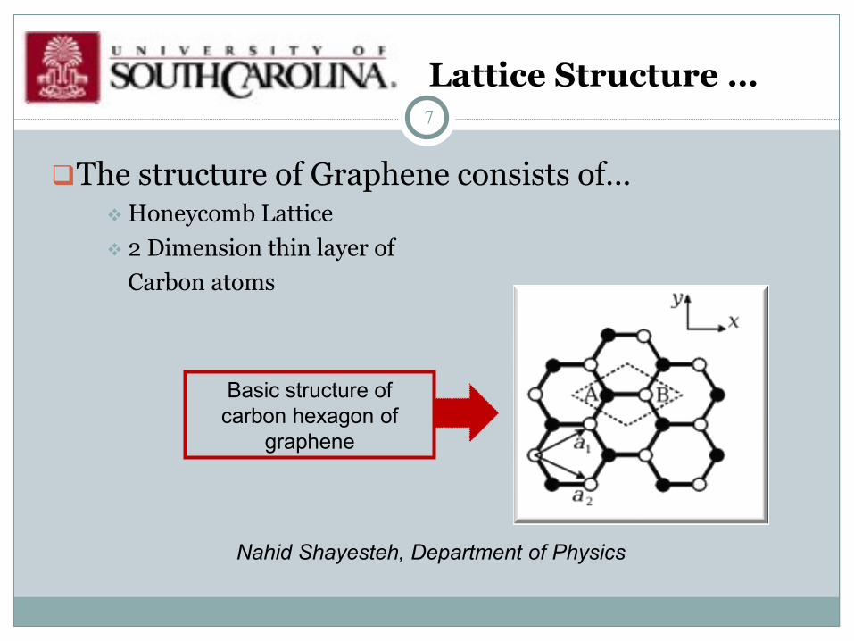
The structure of Graphene consists of… Honeycomb Lattice
2 Dimension thin layer of
Carbon atoms
Basic structure of
carbon hexagon of
graphene
Lattice Structure …
Nahid Shayesteh, Department of Physics

8
The carbon-carbon bond length in graphene is about 0.142 nanometers.
Graphene sheets stack to form graphite.
One stack of 3 million sheets = 1 millimeter thick.
Graphene is the basic structural element of some carbon allotropes including…
Graphite
Charcoal
Carbon Nanotubes
Fullerence
Chemical Structures…
Nahid Shayesteh, Department of Physics

9
The Energy gap of the 1 dimensional graphene nanoribbons (GNRs), can be… Produced lithographically by patterning 2 dimensional
graphene through a chemical route
Different crystallographic orientations
Tuned with varying widths
Energy Gap…
Nahid Shayesteh, physics department

10
Graphene projections…
Display hopeful electronic properties.
(as a conductor of electricity as well as cooper and as a conductor of heat better than all other known materials)
Possess very high electron or hole mobility
(comparable to the properties observed in Carbon nano tubs)
Longest measured mean-free path
High optical transmission
(optical transmission and infrared reflectivity can be tuned as a function of the applied voltage)
In theory…
Nahid Shayesteh, Department of Physics

11
Graphene is considered a semimetal, because…
There is no present band gap (band gap is zero).
There is a narrow channel width (transverse direction) & a
band gap can be provided.
Nahid Shayesteh, Department of physics
12
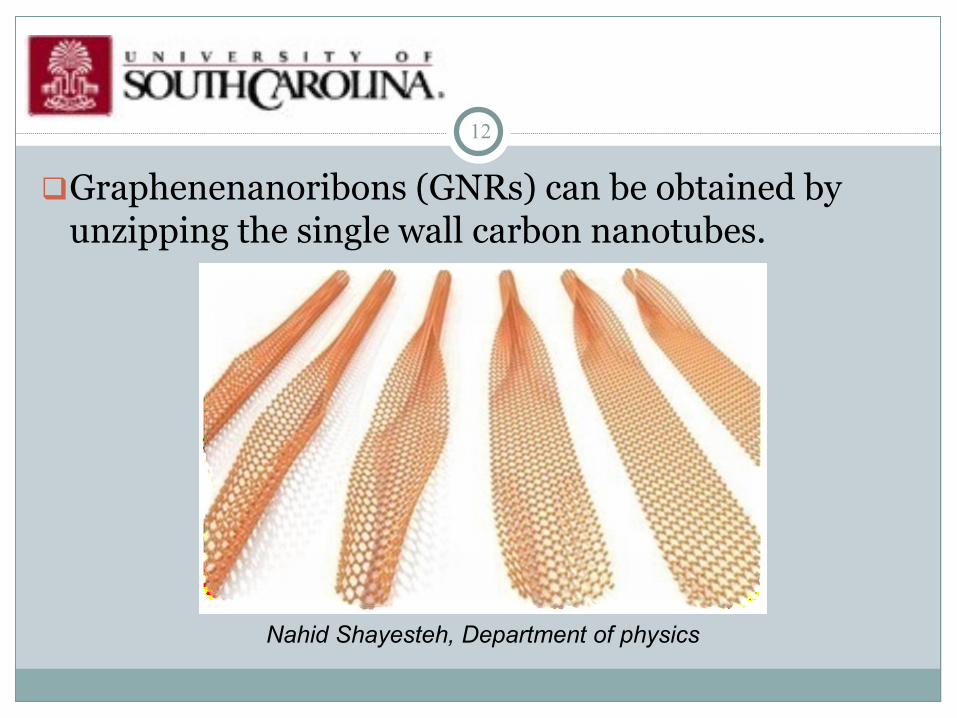
Graphenenanoribons (GNRs) can be obtained by unzipping the single wall carbon nanotubes.
Nahid Shayesteh, Department of physics

13
The ribbon form of graphene (GNR) Inherited almost all of the attractive properties of the carbon nanotube
and graphene.
Additional benefit of a tunable band gap.
Tunable semiconducting behaviors vis a vis changing ribbon width.
The first bandgap measurements are made by... Phaedon Avouris.
Philip Kim
Opening of energy gaps… Reported: 0.5 eV in a 2.5 nm wide armchair ribbon
Electronic Properties…
Nahid Shayesteh, Department of Physics

14
Zigzag & Armchair GNRs are metallic or semiconducting electronic properties that depends on the width of the nanoribbon.
Electronic properties depend on…
the edge shape
1. armchair
2. zigzag
Nahid Shayesteh, Department of Physics
Electronic Properties…

15
Liang work shows certain armchair GNRs can display semiconducting behavior.
Armchair ribbon is semiconducting when N=3p or
N=3p+1
#of dimer lines N=3p+2 is semimetal behavior
(p is integer).
Armchair GNR’s…
Nahid Shayesteh, Department of Physics

16
Zigzag GNRs are either…
1. Semiconducting
2. Metallic
And
Expected to be more conductive
Zigzag GNR’s…
Nahid Shayesteh, Department of Physics
17
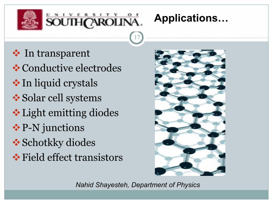
In transparent
Conductive electrodes
In liquid crystals
Solar cell systems
Light emitting diodes
P-N junctions
Schotkky diodes
Field effect transistors
Nahid Shayesteh, Department of Physics
Applications…

18
A p–n junction is formed at the boundary between a p-typeeand n-type semiconductor-type created in a single crystal of semiconductor by doping.
A Schotkky is a special case of a p–n junction, where metal serves the role of the n-type semiconductor.
Nahid Shayesteh, Department of Physics
Junctions…
19
A transistor is a semiconductor device used to amplify and switch electronic signals and power.
The field-effect transistor (FET) is a transistor that relies on an electric field to control the conductivity of a channel of one type of charge carrier in a semiconductor material.
Nahid Shayesteh, Department of Physics
Transistors…

20
New types of the graphene base material can be achieved.
Carbon based material have different application depend on their structure.
Conclusion…
Nahid Shayesteh, Department of Physics

21
References…
1.Bu, H., et al., Atomistic simulations of mechanical properties of
graphene nanoribbons. Physics Letters A, 2009. 373(37): p. 3359-3362.
2.Eduardo V Castro1, N.M.R.P., J M B Lopes dos Santos1, and
F.G.a.A.H.C. Neto4, Bilayer graphene: gap tunability and edge
properties. Journal of Physics, 2010. 129(1): p. 012002(8).
3.connor, O., Liu,, CNTFET Modeling and Recongurable Logic-Circuit
Design. Ieee Transactions on Circuits and Systems, 2007. 54(11): p.
2365-2379.
4.Group, C.M., Moore' s Law: More or Less. www.
cmg.org/measureits/issues/mit41/m_41 2.html, 2010.
5.Novoselov, K.S., Electronic properties of graphene. phys. stat. sol. ,
2007. 244(11 / DOI 10.1002/pssb.200776208): p. 4106-4111.

22
Thank you for your time and
consideration. I will be more than happy to answer any questions or concerns that you may have at this
time.