1 intro signal integrity basics and measurement solutions · signal integrity engineering is at all...
TRANSCRIPT
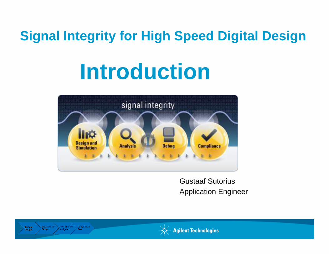
Signal Integrity for High Speed Digital Design
Introduction
Gustaaf SutoriusApplication Engineer
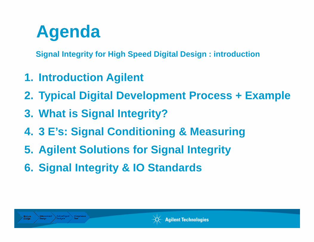
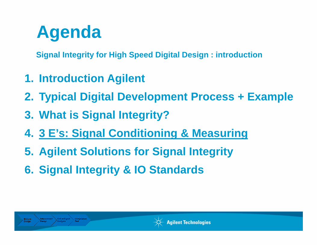
AgendaSignal Integrity for High Speed Digital Design : int roduction
1. Introduction Agilent
2. Typical Digital Development Process + Example
3. What is Signal Integrity?
4. 3 E’s: Signal Conditioning & Measuring
5. Agilent Solutions for Signal Integrity
6. Signal Integrity & IO Standards

AgendaSignal Integrity for High Speed Digital Design : int roduction
1. Introduction Agilent
2. Typical Digital Development Process + Example
3. What is Signal Integrity?
4. 3 E’s: Signal Conditioning & Measuring
5. Agilent Solutions for Signal Integrity
6. Signal Integrity & IO Standards
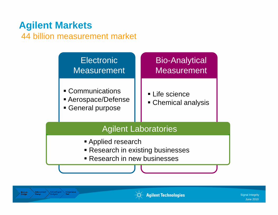
Agilent Markets44 billion measurement market
Bio-AnalyticalMeasurement� Life science� Chemical analysis
� Communications� Aerospace/Defense� General purpose
ElectronicMeasurement
Bio-AnalyticalMeasurement
Signal Integrity
June 2010
� General purpose
� Applied research� Research in existing businesses� Research in new businesses
Agilent Laboratories
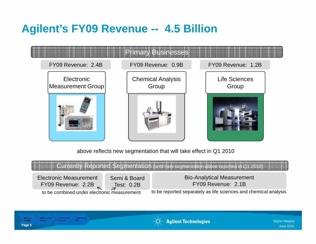
Agilent’s FY09 Revenue -- 4.5 Billion
LTM Revenue*1.1B
LTM Revenue*1.0B
LTM Revenue*2.7B
Primary Businesses
Electronic Measurement Group
Chemical Analysis Group
Life SciencesGroup
FY09 Revenue: 2.4B FY09 Revenue: 0.9B FY09 Revenue: 1.2B
Page 5Page 5Page 5
above reflects new segmentation that will take effect in Q1 2010
Electronic MeasurementFY09 Revenue: 2.2B
Bio-Analytical MeasurementFY09 Revenue: 2.1B
Semi & Board Test: 0.2B
Currently Reported Segmentation (until new segmentation above reported in Q1 2010)
to be combined under electronic measurement to be reported separately as life sciences and chemical analysis
June 2010
Signal Integrity
AgendaSignal Integrity for High Speed Digital Design : int roduction
1. Introduction Agilent
2. Typical Digital Development Process + Example
3. What is Signal Integrity?
4. 3 E’s: Signal Conditioning & Measuring
5. Agilent Solutions for Signal Integrity
6. Signal Integrity & IO Standards

Typical Digital Development Process
• Accurate Models• Accurate
Simulations
SystemDesign
InterconnectDesign
Active SignalAnalysis
ComplianceTest
• Accurate Models & Simulations
• Accurate Design Analysis
• Accurate Design Analysis
• Test & Analysis Capability
• Increased Team Effectiveness
• Measurement Automation• Hardware &
Software Correlation
Analysis• Hardware &
SoftwareCorrelation
Capability• Measurement
Automation
Automation• Test & Analysis
Capability
Measure

Signal Integrity Solutions Portfolio (assisting this digital development process)

Actual Development Example: SDR in FPGA
SystemDesign
InterconnectDesign
Active SignalAnalysis
ComplianceTest
• Accurate Models & Simulations
• Accurate Design Analysis
• Accurate Design Analysis
• Test & Analysis CapabilityAnalysis
• Hardware & SoftwareCorrelation
Capability• Measurement
Automation
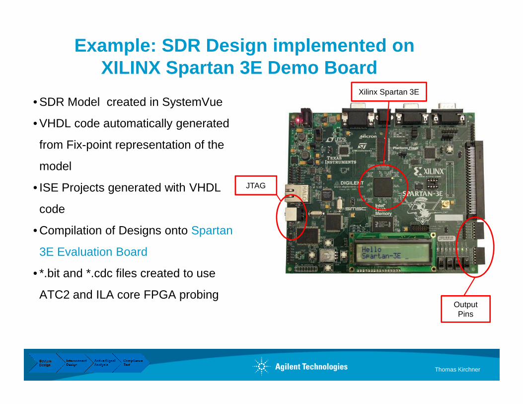
Example: SDR Design implemented on XILINX Spartan 3E Demo Board
• SDR Model created in SystemVue
• VHDL code automatically generated
from Fix-point representation of the
model
• ISE Projects generated with VHDL JTAG
Xilinx Spartan 3E
code
• Compilation of Designs onto Spartan
3E Evaluation Board
• *.bit and *.cdc files created to use
ATC2 and ILA core FPGA probingOutput Pins
Thomas Kirchner
Flow1. Develop a model for a digital Software Defined Radio
Design using SystemVue from Agilent eeSof
2. Verification of model (modulated IQ-signal) using VSA SW in SystemVue
3. Generate VHDL code from SystemVue Model
4. Create a XILINX ISE Project with VHDL code from SystemVue. And put this in the Spartan 3E SystemVue. And put this in the Spartan 3E
5. Insert ILA core and debug FPGA design using XILINX Chipscope
6. Insert Agilent ATC2 core and debug design using Agilent dynamic FPGA probe in Logic Analyzer
7. Verify design and decode digital IQ data using Agilent Logic Analyzer and IQ demodulator (VSA 89601A SW)
Seite 2 von 24 Thomas Kirchner
Why this Flow
• Software Defined Radio Design is complex and needs to be flexible to
adjust feature to requirements
•High level System Design Model is needed and the ability of automated
VHDL code generation
•Complex Designs require Debug- and Verification using Timing-, State-
and PHYS Layer Characterization
Seite 3 von 24 Thomas Kirchner
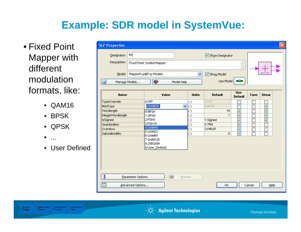
Example: SDR model in SystemVue:
• Fixed Point Mapper with different modulation formats, like:
• QAM16
• BPSK• BPSK
• QPSK
• ...
• User Defined
Thomas Kirchner
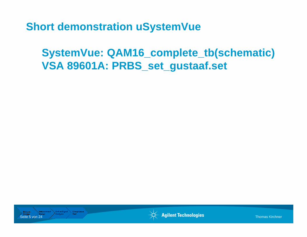
Short demonstration uSystemVue
SystemVue: QAM16_complete_tb(schematic)VSA 89601A: PRBS_set_gustaaf.set
Seite 5 von 24 Thomas Kirchner

Verification of modulated IQ-signal using VSA SW in SystemVue:
Thomas Kirchner
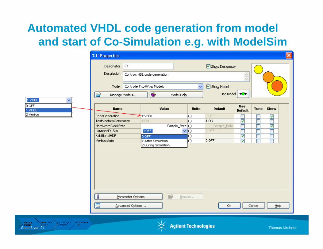
Automated VHDL code generation from model and start of Co-Simulation e.g. with ModelSim
Seite 5 von 24 Thomas Kirchner
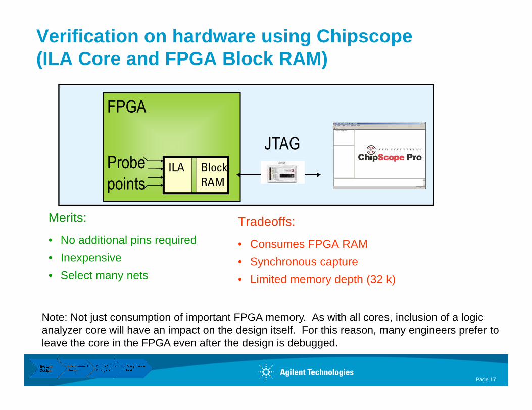
Verification on hardware using Chipscope(ILA Core and FPGA Block RAM)
ILA Block
RAM
FPGA
JTAGProbe
points
Page 17
Merits:
• No additional pins required
• Inexpensive
• Select many nets
Tradeoffs:
• Consumes FPGA RAM
• Synchronous capture
• Limited memory depth (32 k)
Note: Not just consumption of important FPGA memory. As with all cores, inclusion of a logic analyzer core will have an impact on the design itself. For this reason, many engineers prefer to leave the core in the FPGA even after the design is debugged.

ATC2
Selection M
UX
4 -128
4 - 128
4 - 128
4 - 128
Output to FPGA pins for debug
Verification on hardware using Agilent Trace Core (ATC2)
• Up to 64 signal banks
• All banks have identical width (4 to 128 signals wide)
Rapid Debug of FPGA-based Systems using MSOs, 4/2/2011Page 18
Selection M
UX
4 -128
Change signal bank selection from MSO`
JTA
G S
elec
t
clkclk Up to 16 digital channelson MSOs
128 channels on Logic Analyzer
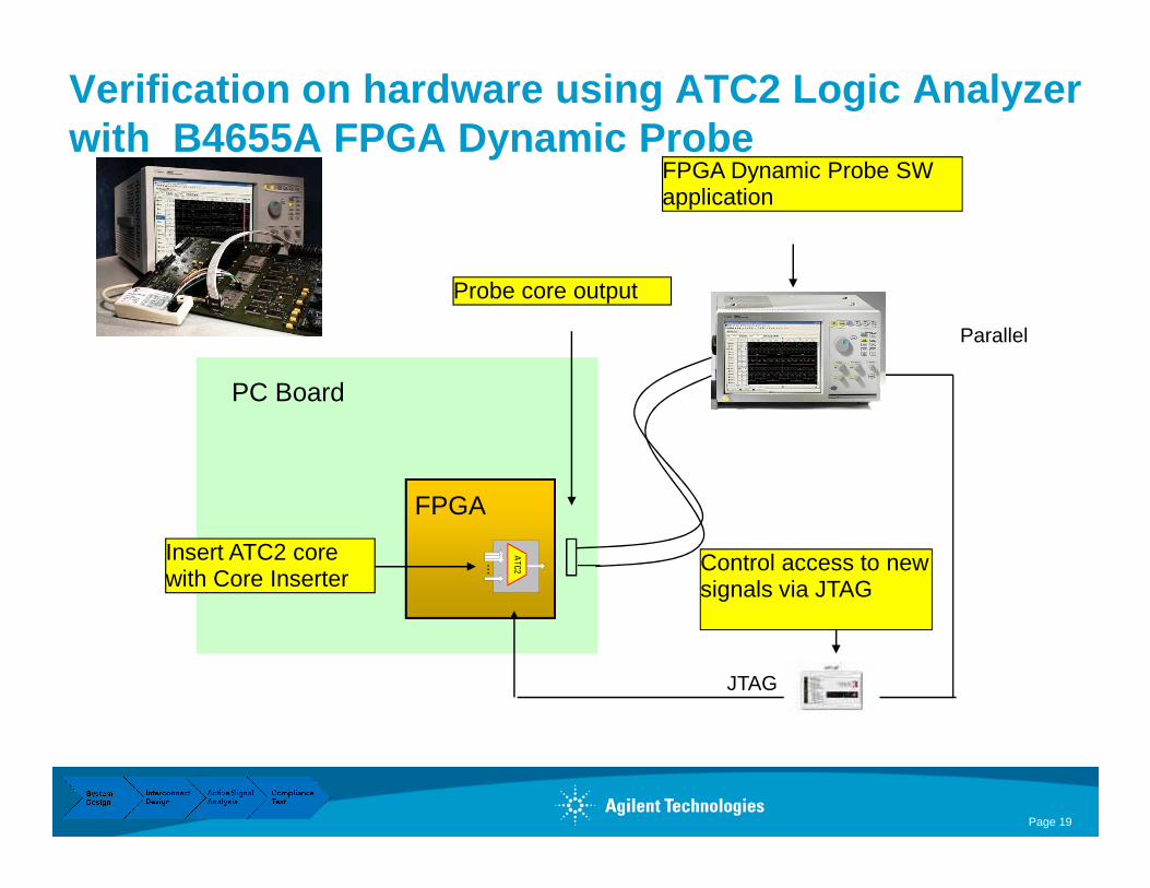
Verification on hardware using ATC2 Logic Analyzer with B4655A FPGA Dynamic Probe
PC Board
FPGA Dynamic Probe SW application
Parallel
Probe core output
Page 19
ATC2
Insert ATC2 core with Core Inserter
FPGA
JTAG
Control access to new signals via JTAG
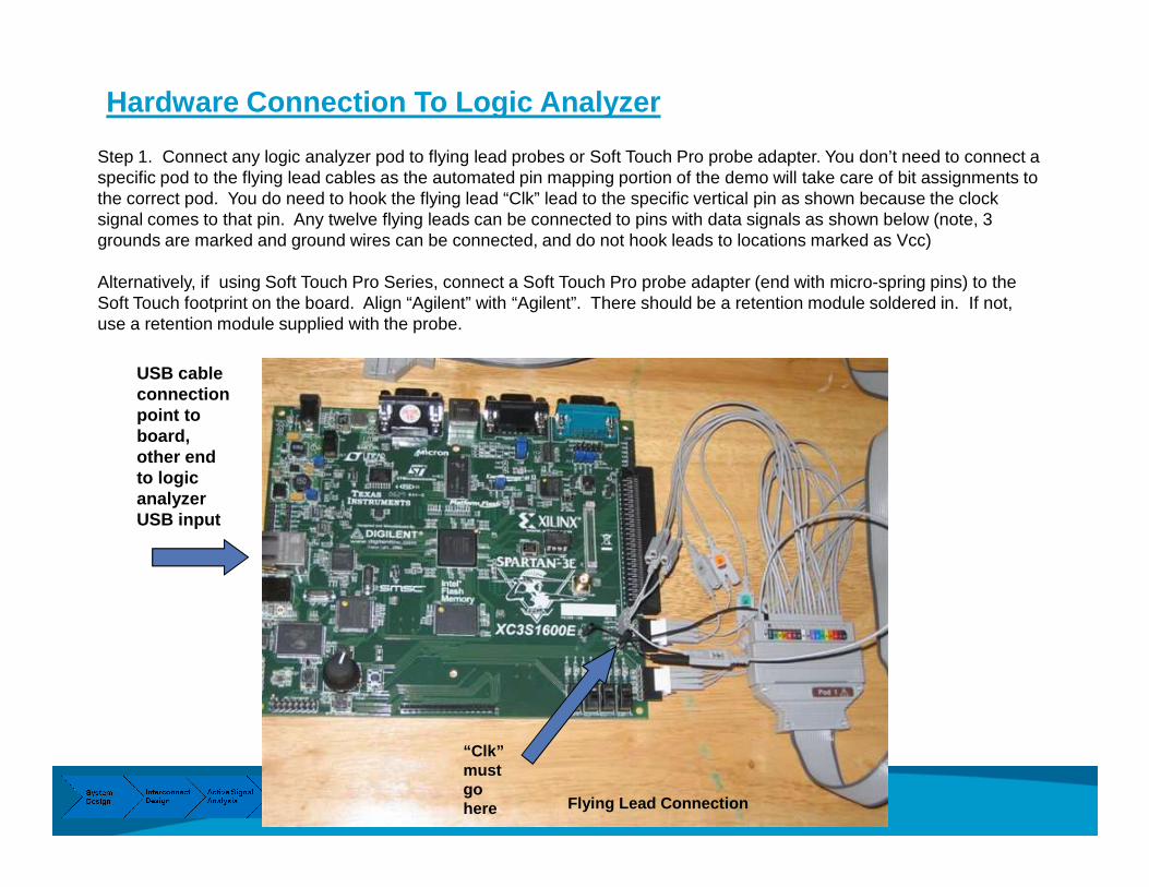
Step 1. Connect any logic analyzer pod to flying lead probes or Soft Touch Pro probe adapter. You don’t need to connect a specific pod to the flying lead cables as the automated pin mapping portion of the demo will take care of bit assignments to the correct pod. You do need to hook the flying lead “Clk” lead to the specific vertical pin as shown because the clock signal comes to that pin. Any twelve flying leads can be connected to pins with data signals as shown below (note, 3 grounds are marked and ground wires can be connected, and do not hook leads to locations marked as Vcc)
Alternatively, if using Soft Touch Pro Series, connect a Soft Touch Pro probe adapter (end with micro-spring pins) to the Soft Touch footprint on the board. Align “Agilent” with “Agilent”. There should be a retention module soldered in. If not,use a retention module supplied with the probe.
Hardware Connection To Logic Analyzer
USB cable connection point to board,
Flying Lead Connection
board, other end to logic analyzer USB input
“Clk” must go here
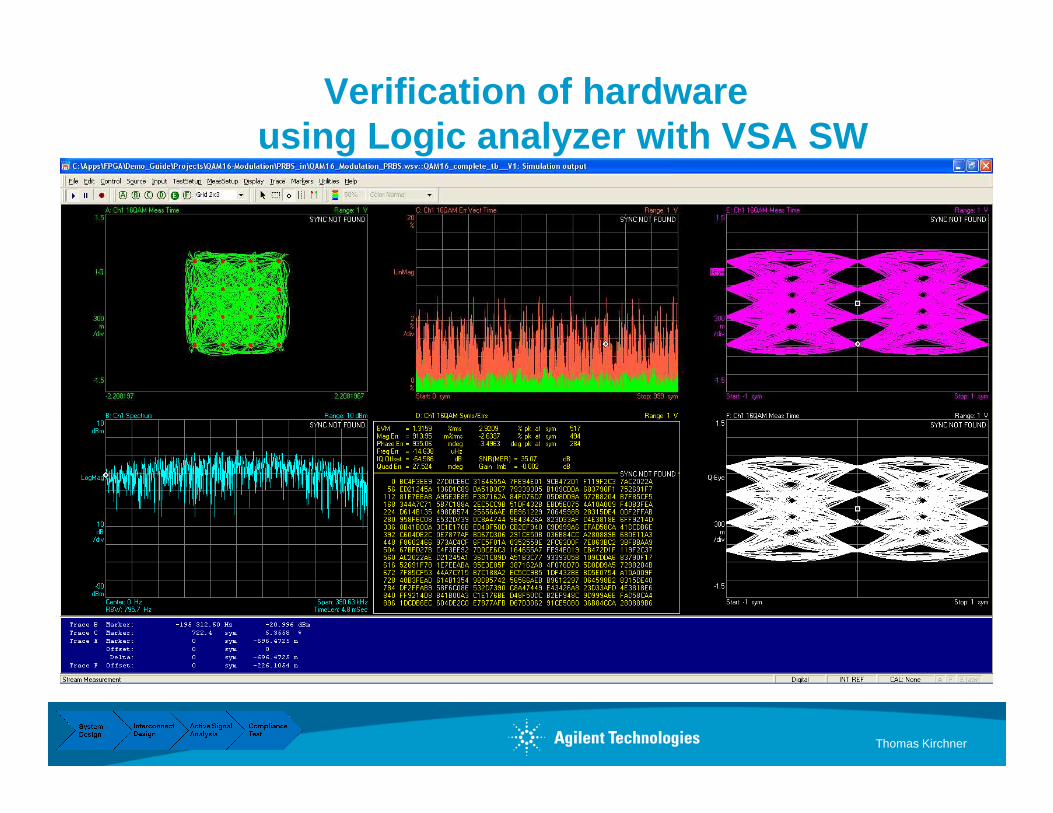
Verification of hardware using Logic analyzer with VSA SW
Thomas Kirchner

Short demonstration using N5406A FPGA dynamic probe on oscilloscope
Seite 5 von 24 Thomas Kirchner
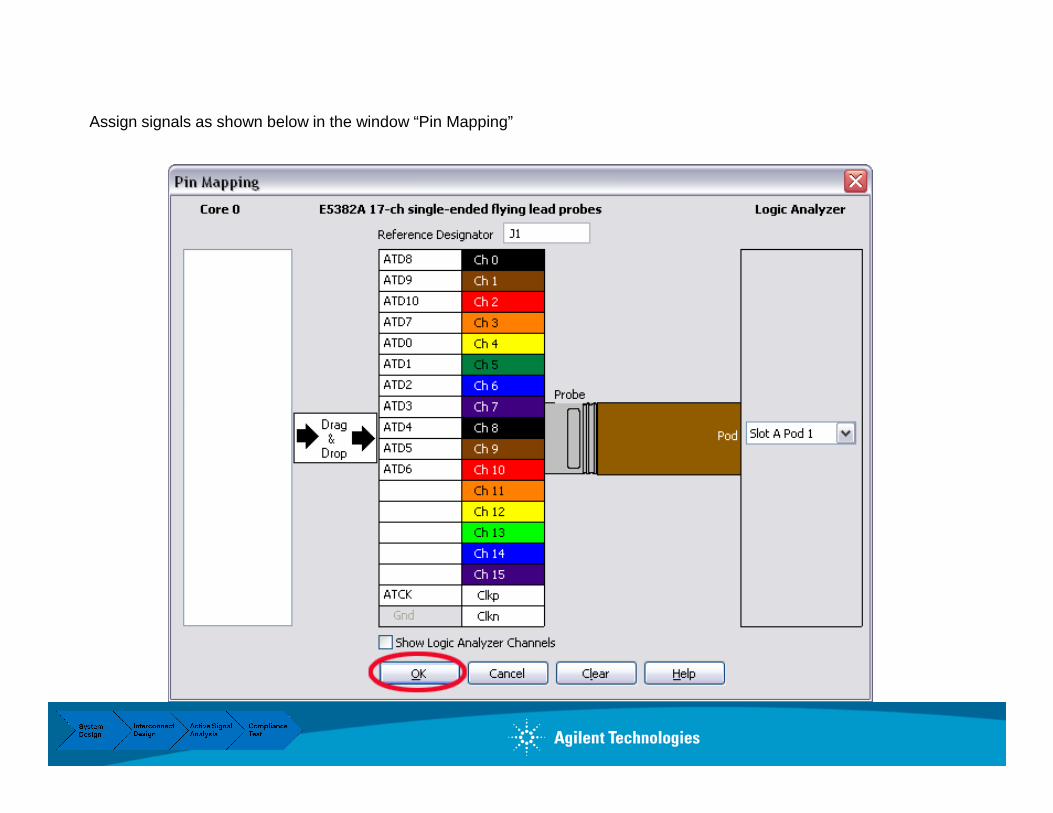
Assign signals as shown below in the window “Pin Mapping”

Analysis of PRBS-Generator with Chipscope ILA
• PRBS Signal is captured by Chipscope ILA Core and stored in Block RAM• Data are read out to Chipscope Program on PC• Cost effective solution – does not require LA or MSO• RAM Resources are rare and limited size• No correlation to external signals possible• For changes of Trigger, new compilation of the ILA Core has to be done• This Example: Comparison of PRBS Polynom with reference from Agilent Pattern Generator
Thomas Kirchner
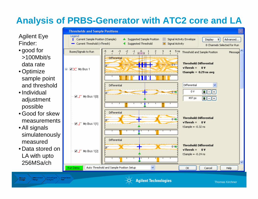
Analysis of PRBS-Generator with ATC2 core and LA
Agilent Eye Finder: • good for >100Mbit/s data rate
• Optimize sample point and threshold
• Individual adjustment adjustment possible
• Good for skew measurements
• All signals simulatenously measured
• Data stored on LA with upto 256MSa/ch
Thomas Kirchner

AgendaSignal Integrity for High Speed Digital Design : int roduction
1. Introduction Agilent
2. Typical Digital Development Process + Example
3. What is Signal Integrity?
4. 3 E’s: Signal Conditioning & Measuring
5. Agilent Solutions for Signal Integrity
6. Signal Integrity & IO Standards
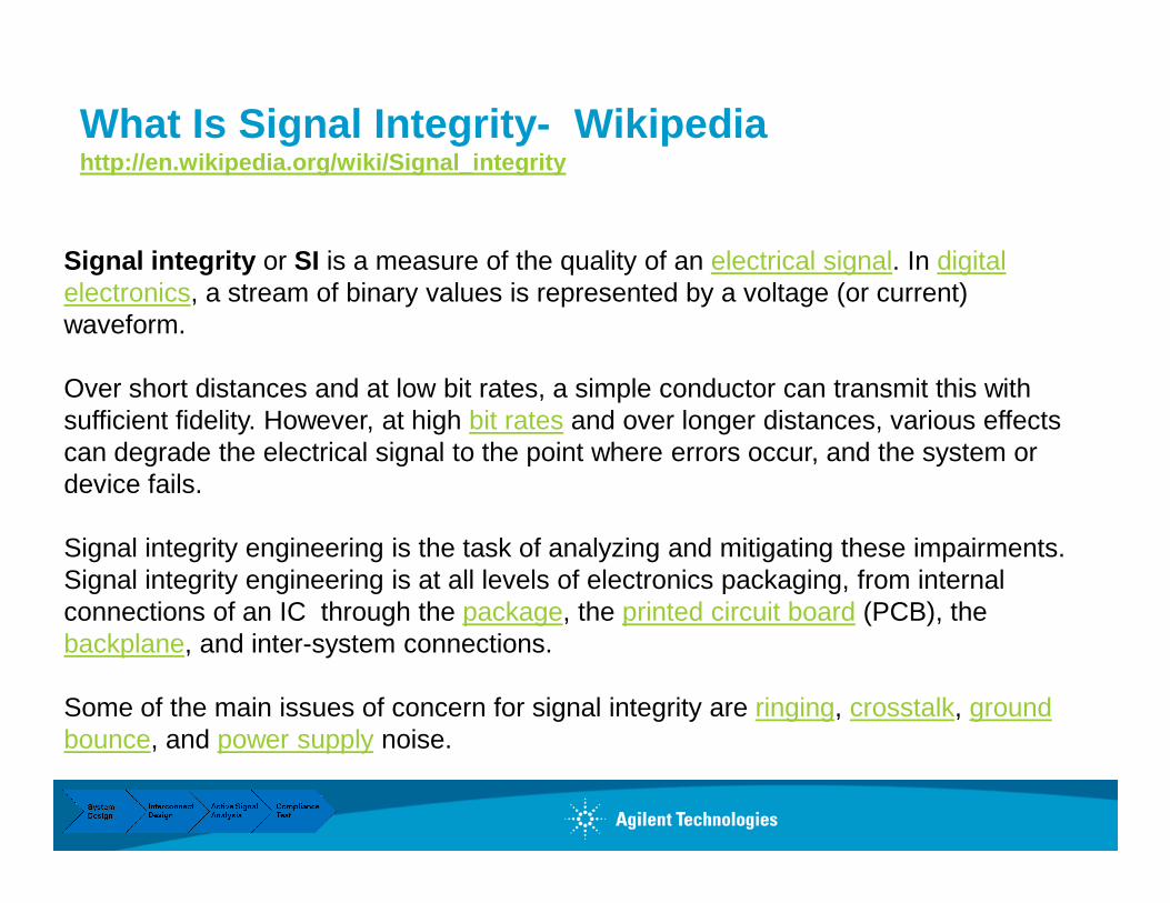
What Is Signal Integrity- Wikipedia http://en.wikipedia.org/wiki/Signal_integrity
Signal integrity or SI is a measure of the quality of an electrical signal. In digital electronics, a stream of binary values is represented by a voltage (or current) waveform.
Over short distances and at low bit rates, a simple conductor can transmit this with sufficient fidelity. However, at high bit rates and over longer distances, various effects can degrade the electrical signal to the point where errors occur, and the system or can degrade the electrical signal to the point where errors occur, and the system or device fails.
Signal integrity engineering is the task of analyzing and mitigating these impairments. Signal integrity engineering is at all levels of electronics packaging, from internal connections of an IC through the package, the printed circuit board (PCB), the backplane, and inter-system connections.
Some of the main issues of concern for signal integrity are ringing, crosstalk, ground bounce, and power supply noise.

Signal Integrity- Challenges In Digital Design Today
• Higher Data Rates Are Causing Signal Integrity (SI) Problems:• Need to include high-frequency effects like
interconnects in simulation and layout• Need high quality probes and fixtures• Need to minimize jitter
• FPGAs Are Commonplace:• Can’t use a Reference Design without some• Can’t use a Reference Design without some
analysis• Harder to simulate the overall performance• Need to characterize the I/O buffers
• Standards Evolve Every 2-3 Years:• Leveraging existing designs gets harder• Measurement requirements get tighter• Need to buy new equipment each time
2.5 Gb/s
5 Gb/s
8 Gb/s
2003 2008
2006 2011
2009 2014
PCI Express

Data Rates Of Key Serial I/O Technologies
PCI Express
Serial ATA
SAS
Fibre Channel
USB 5G480M
2.5G 5G 8G
1.5G 3G 6G
1.5G 3G 6G
1G 2G 4G 8G 16G
0 1 2 3 4 5 6 7 8 9 10 11 12 13 14 15 16 Gb/s
Ethernet
DisplayPort
AvailablePlanned
HDMI
FB-DIMM
DDR
1G 3.125 (XAUI) 10G
4.8G 9.6G
1G
1.6G 3.4G
2.7G
1.6G
5.4G
Signal Integrity is important
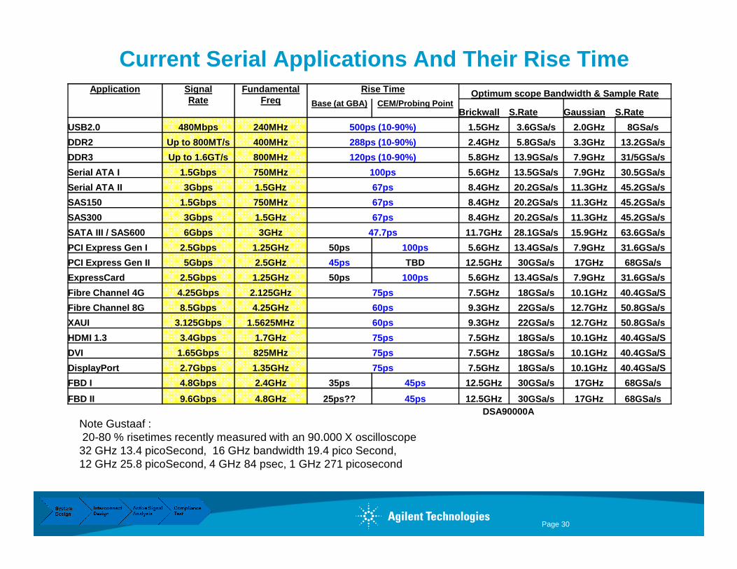
Current Serial Applications And Their Rise TimeApplication Signal
RateFundamental
FreqRise Time Optimum scope Bandwidth & Sample Rate
Base (at GBA) CEM/Probing PointBrickwall S.Rate Gaussian S.Rate
USB2.0 480Mbps 240MHz 500ps (10-90%) 1.5GHz 3.6GSa/s 2.0GHz 8GSa/s
DDR2 Up to 800MT/s 400MHz 288ps (10-90%) 2.4GHz 5.8GSa/s 3.3GHz 13.2GSa/s
DDR3 Up to 1.6GT/s 800MHz 120ps (10-90%) 5.8GHz 13.9GSa/s 7.9GHz 31/5GSa/s
Serial ATA I 1.5Gbps 750MHz 100ps 5.6GHz 13.5GSa/s 7.9GHz 30.5GSa/s
Serial ATA II 3Gbps 1.5GHz 67ps 8.4GHz 20.2GSa/s 11.3GHz 45.2GSa/s
SAS150 1.5Gbps 750MHz 67ps 8.4GHz 20.2GSa/s 11.3GHz 45.2GSa/s
SAS300 3Gbps 1.5GHz 67ps 8.4GHz 20.2GSa/s 11.3GHz 45.2GSa/s
SATA III / SAS600 6Gbps 3GHz 47.7ps 11.7GHz 28.1GSa/s 15.9GHz 63.6GSa/s
PCI Express Gen I 2.5Gbps 1.25GHz 50ps 100ps 5.6GHz 13.4GSa/s 7.9GHz 31.6GSa/s
PCI Express Gen II 5Gbps 2.5GHz 45ps TBD 12.5GHz 30GSa/s 17GHz 68GSa/s
ExpressCard 2.5Gbps 1.25GHz 50ps 100ps 5.6GHz 13.4GSa/s 7.9GHz 31.6GSa/s
Page 30
Fibre Channel 4G 4.25Gbps 2.125GHz 75ps 7.5GHz 18GSa/s 10.1GHz 40.4GSa/S
Fibre Channel 8G 8.5Gbps 4.25GHz 60ps 9.3GHz 22GSa/s 12.7GHz 50.8GSa/s
XAUI 3.125Gbps 1.5625MHz 60ps 9.3GHz 22GSa/s 12.7GHz 50.8GSa/s
HDMI 1.3 3.4Gbps 1.7GHz 75ps 7.5GHz 18GSa/s 10.1GHz 40.4GSa/S
DVI 1.65Gbps 825MHz 75ps 7.5GHz 18GSa/s 10.1GHz 40.4GSa/S
DisplayPort 2.7Gbps 1.35GHz 75ps 7.5GHz 18GSa/s 10.1GHz 40.4GSa/S
FBD I 4.8Gbps 2.4GHz 35ps 45ps 12.5GHz 30GSa/s 17GHz 68GSa/s
FBD II 9.6Gbps 4.8GHz 25ps?? 45ps 12.5GHz 30GSa/s 17GHz 68GSa/sDSA90000A
Note Gustaaf :20-80 % risetimes recently measured with an 90.000 X oscilloscope 32 GHz 13.4 picoSecond, 16 GHz bandwidth 19.4 pico Second, 12 GHz 25.8 picoSecond, 4 GHz 84 psec, 1 GHz 271 picosecond
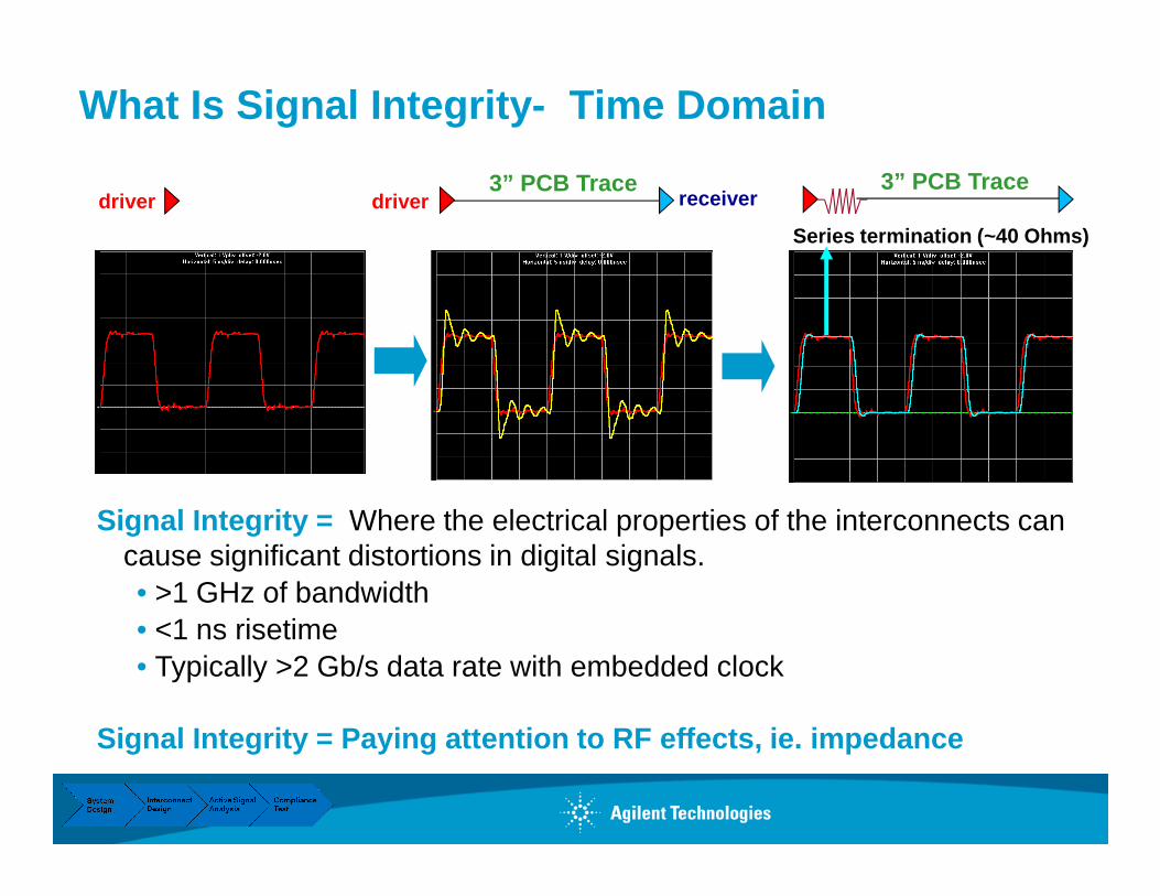
What Is Signal Integrity- Time Domain
driver receiver
Series termination (~40 Ohms)
3” PCB Trace3” PCB Tracedriver
Signal Integrity = Where the electrical properties of the interconnects can cause significant distortions in digital signals.• >1 GHz of bandwidth• <1 ns risetime• Typically >2 Gb/s data rate with embedded clock
Signal Integrity = Paying attention to RF effects, ie. impedance

What Is Signal Integrity - Four Signal Integrity Problems And Their Causes1. Poor signal quality of one net: reflections and
distortions from impedance discontinuities in the signal or return path
2. Crosstalk between multiple nets: mutual C and mutual L coupling
3. Rail collapse (Ground Bounce) in the power 3. Rail collapse (Ground Bounce) in the power distribution system: voltage drops across impedance in the power/ground network
4. Jitter from causes listed above and variety of other sources including clock distribution, data dependent effects, and EMI
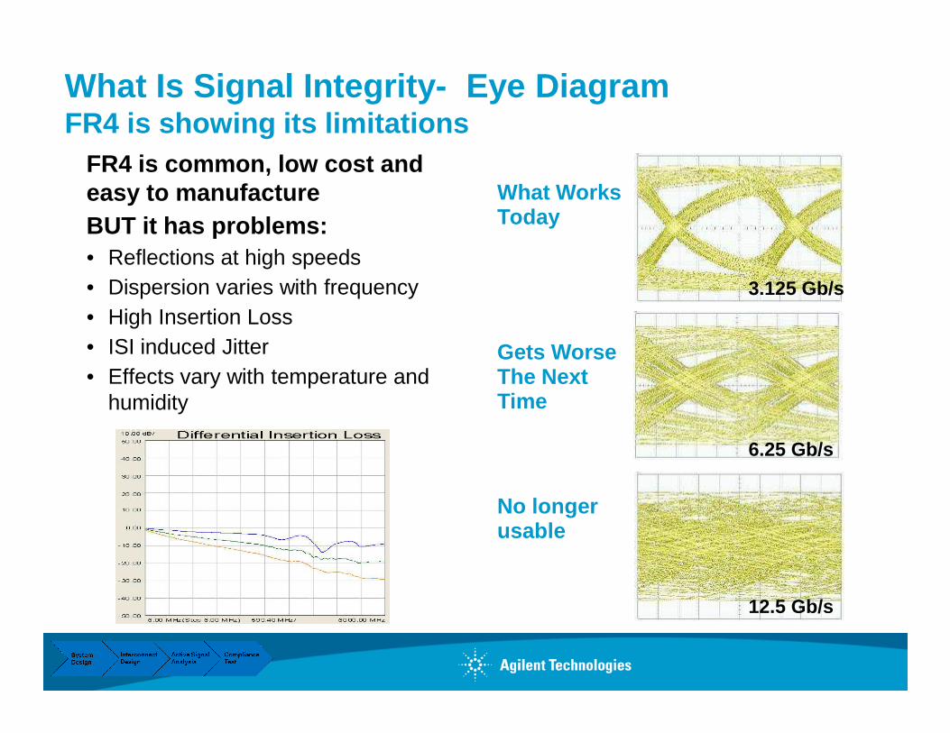
What Is Signal Integrity- Eye DiagramFR4 is showing its limitations
FR4 is common, low cost and easy to manufactureBUT it has problems:• Reflections at high speeds• Dispersion varies with frequency• High Insertion Loss• ISI induced Jitter• Effects vary with temperature and
What Works Today
Gets Worse The Next
3.125 Gb/s
• Effects vary with temperature and humidity
The Next Time
No longer usable
6.25 Gb/s
12.5 Gb/s
AgendaSignal Integrity for High Speed Digital Design : int roduction
1. Introduction Agilent
2. Typical Digital Development Process + Example
3. What is Signal Integrity?
4. 3 E’s: Signal Conditioning & Measuring
5. Agilent Solutions for Signal Integrity
6. Signal Integrity & IO Standards
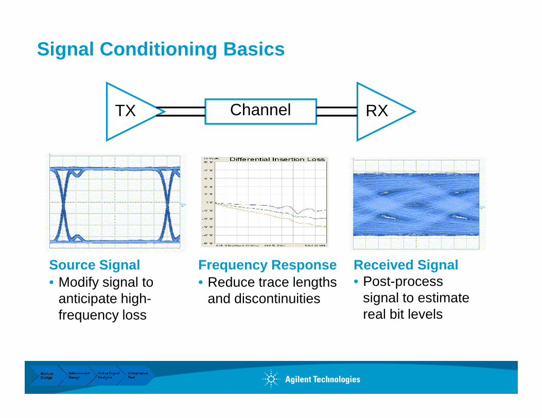
Signal Conditioning Basics
TX RXChannel
Source Signal• Modify signal to
anticipate high-frequency loss
Received Signal• Post-process
signal to estimate real bit levels
Frequency Response• Reduce trace lengths
and discontinuities
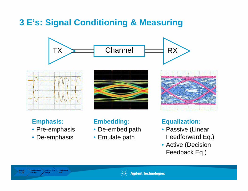
3 E’s: Signal Conditioning & Measuring
TX RXChannel
Emphasis:• Pre-emphasis• De-emphasis
Equalization:• Passive (Linear
Feedforward Eq.)• Active (Decision
Feedback Eq.)
Embedding:• De-embed path• Emulate path

AgendaSignal Integrity for High Speed Digital Design : int roduction
1. Introduction Agilent
2. Typical Digital Development Process + Example
3. What is Signal Integrity?
4. 3 E’s: Signal Conditioning & Measuring
5. Agilent Solutions for Signal Integrity
6. Signal Integrity & IO Standards
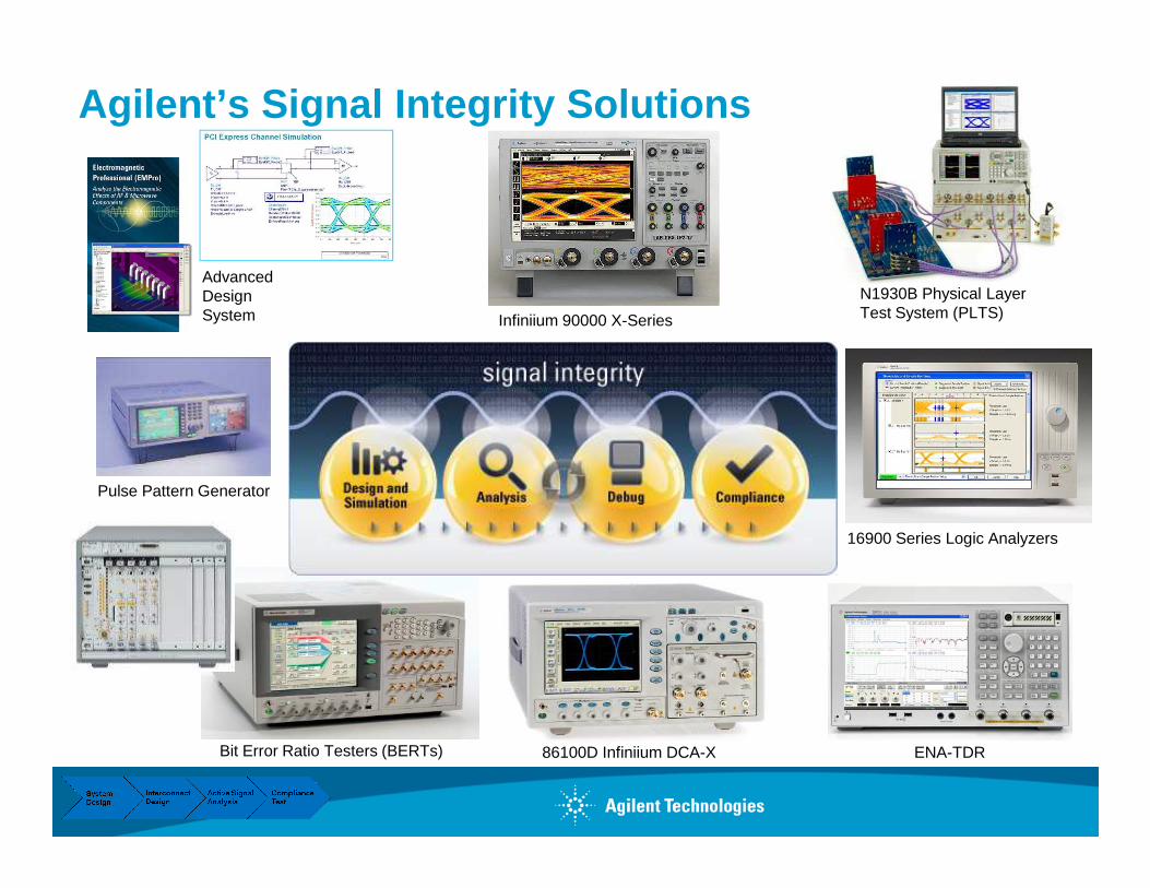
Agilent’s Signal Integrity Solutions
Advanced Design System Infiniium 90000 X-Series
N1930B Physical Layer Test System (PLTS)
Bit Error Ratio Testers (BERTs) 86100D Infiniium DCA-X ENA-TDR
16900 Series Logic Analyzers
Pulse Pattern Generator
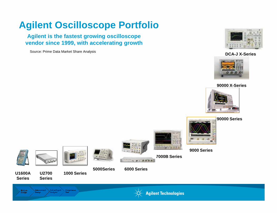
Agilent Oscilloscope Portfolio
DCA-J X-Series
90000 X-Series
Agilent is the fastest growing oscilloscope vendor since 1999, with accelerating growth
Source: Prime Data Market Share Analysis
7000B Series
5000Series 1000 Series U1600A
Series
6000 Series U2700Series
9000 Series
90000 Series
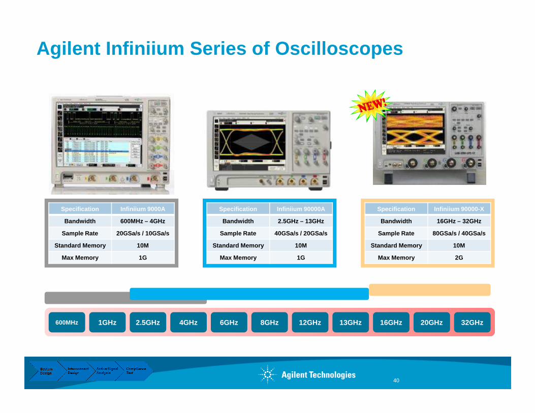
Agilent Infiniium Series of Oscilloscopes
Specification Infiniium 90000-XSpecification Infiniium 90000ASpecification Infiniium 9000A
40
Specification Infiniium 90000-X
Bandwidth 16GHz – 32GHz
Sample Rate 80GSa/s / 40GSa/s
Standard Memory 10M
Max Memory 2G
Specification Infiniium 90000A
Bandwidth 2.5GHz – 13GHz
Sample Rate 40GSa/s / 20GSa/s
Standard Memory 10M
Max Memory 1G
Specification Infiniium 9000A
Bandwidth 600MHz – 4GHz
Sample Rate 20GSa/s / 10GSa/s
Standard Memory 10M
Max Memory 1G
600MHz 1GHz 2.5GHz 4GHz 6GHz 8GHz 12GHz 13GHz 16GHz 20GHz 32GHz
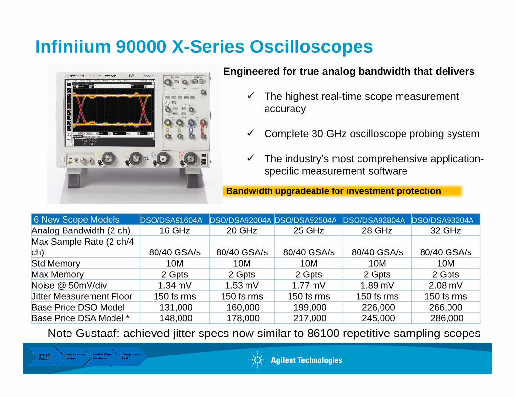
Infiniium 90000 X-Series OscilloscopesEngineered for true analog bandwidth that delivers
� The highest real-time scope measurement accuracy
� Complete 30 GHz oscilloscope probing system
� The industry’s most comprehensive application-specific measurement software
Bandwidth upgradeable for investment protection
6 New Scope Models DSO/DSA91604A DSO/DSA92004A DSO/DSA92504A DSO/DSA92804A DSO/DSA93204AAnalog Bandwidth (2 ch) 16 GHz 20 GHz 25 GHz 28 GHz 32 GHzMax Sample Rate (2 ch/4 ch) 80/40 GSA/s 80/40 GSA/s 80/40 GSA/s 80/40 GSA/s 80/40 GSA/sStd Memory 10M 10M 10M 10M 10MMax Memory 2 Gpts 2 Gpts 2 Gpts 2 Gpts 2 GptsNoise @ 50mV/div 1.34 mV 1.53 mV 1.77 mV 1.89 mV 2.08 mVJitter Measurement Floor 150 fs rms 150 fs rms 150 fs rms 150 fs rms 150 fs rmsBase Price DSO Model 131,000 160,000 199,000 226,000 266,000Base Price DSA Model * 148,000 178,000 217,000 245,000 286,000
Note Gustaaf: achieved jitter specs now similar to 86100 repetitive sampling scopes
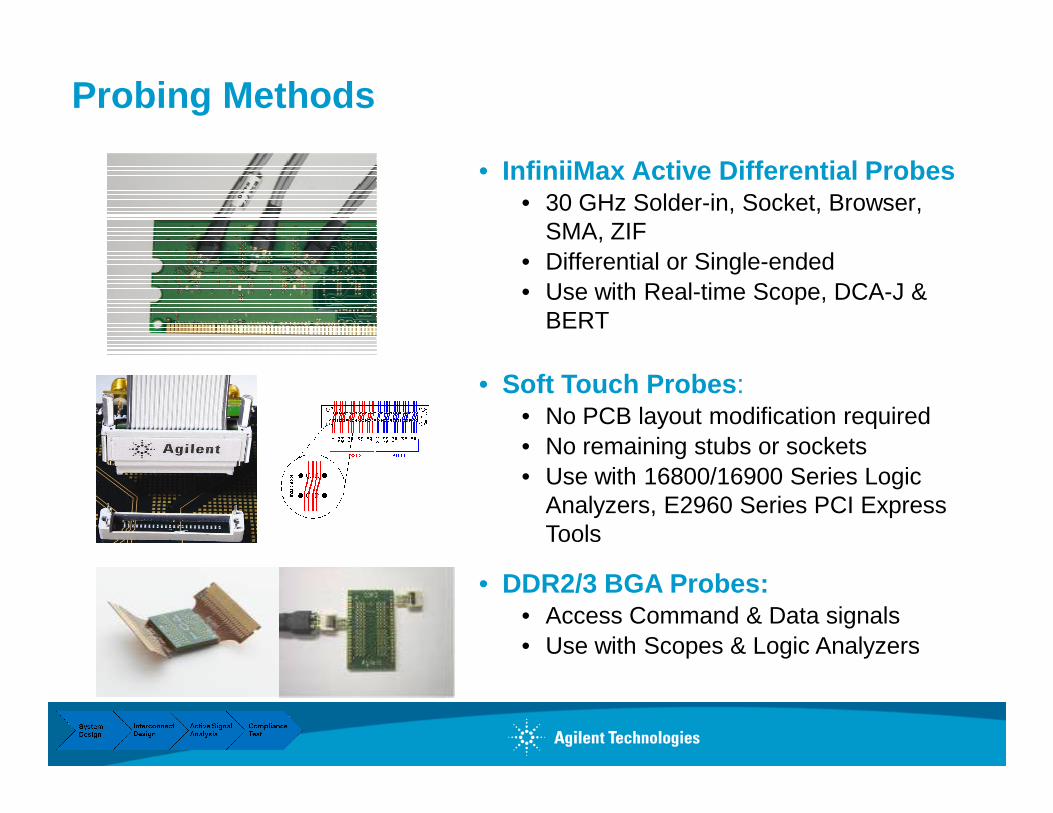
Probing Methods
• InfiniiMax Active Differential Probes• 30 GHz Solder-in, Socket, Browser,
SMA, ZIF• Differential or Single-ended• Use with Real-time Scope, DCA-J &
BERT
• Soft Touch Probes :• No PCB layout modification required• No PCB layout modification required• No remaining stubs or sockets• Use with 16800/16900 Series Logic
Analyzers, E2960 Series PCI Express Tools
• DDR2/3 BGA Probes:• Access Command & Data signals• Use with Scopes & Logic Analyzers
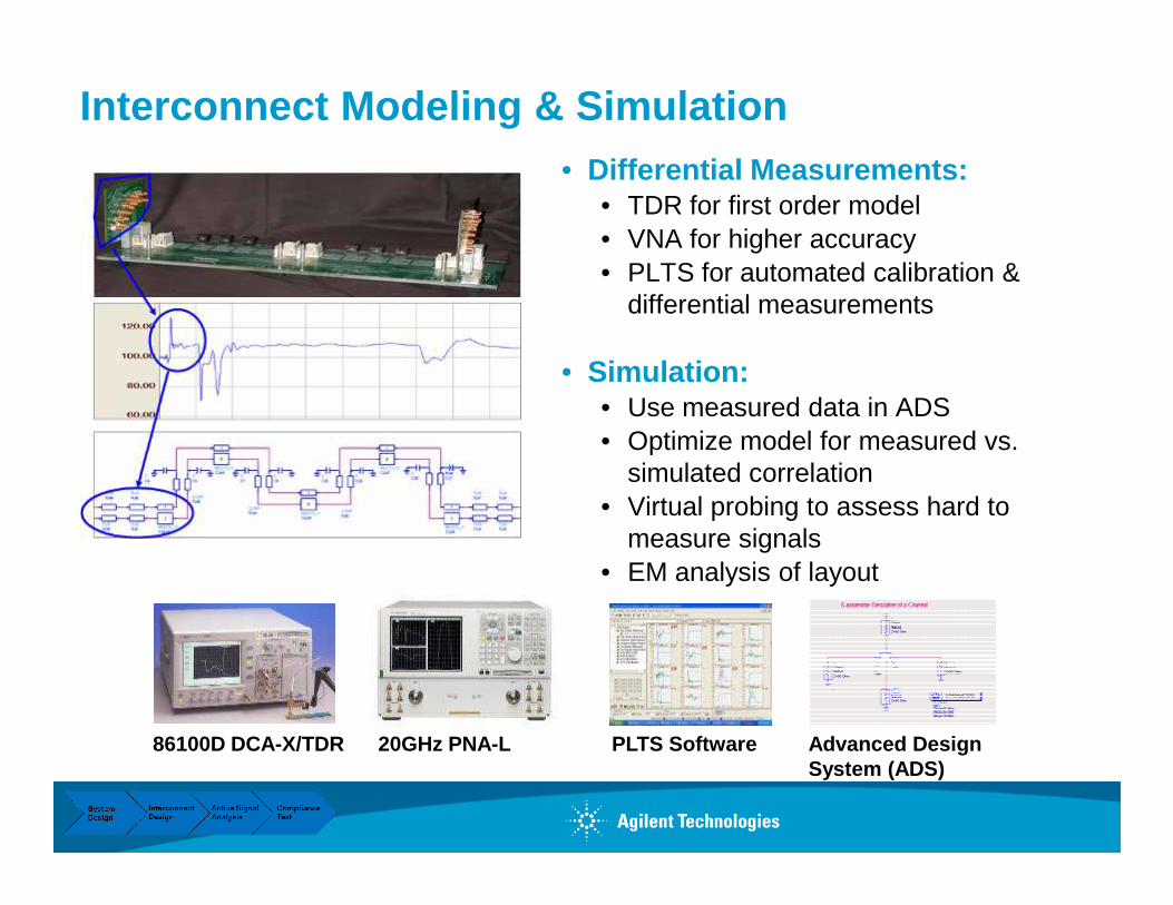
Interconnect Modeling & Simulation• Differential Measurements:
• TDR for first order model• VNA for higher accuracy• PLTS for automated calibration &
differential measurements
• Simulation:• Use measured data in ADS• Optimize model for measured vs. • Optimize model for measured vs.
simulated correlation• Virtual probing to assess hard to
measure signals• EM analysis of layout
86100D DCA-X/TDR 20GHz PNA-L PLTS Software Advanced De sign System (ADS)
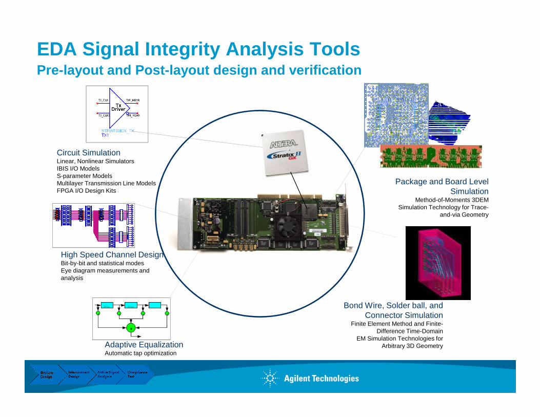
EDA Signal Integrity Analysis Tools
Package and Board LevelSimulation
Method-of-Moments 3DEM Simulation Technology for Trace-
Circuit SimulationLinear, Nonlinear SimulatorsIBIS I/O ModelsS-parameter ModelsMultilayer Transmission Line ModelsFPGA I/O Design Kits
Pre-layout and Post-layout design and verification
Simulation Technology for Trace-and-via Geometry
Bond Wire, Solder ball, and Connector Simulation
Finite Element Method and Finite-Difference Time-Domain
EM Simulation Technologies for Arbitrary 3D Geometry
High Speed Channel DesignBit-by-bit and statistical modesEye diagram measurements and analysis
Adaptive Equalization Automatic tap optimization

AgendaSignal Integrity for High Speed Digital Design : int roduction
1. Introduction Agilent
2. Typical Digital Development Process + Example
3. What is Signal Integrity?
4. 3 E’s: Signal Conditioning & Measuring
5. Agilent Solutions for Signal Integrity
6. Signal Integrity & IO Standards

Typical Digital Development Process
SystemDesign
InterconnectDesign
Active SignalAnalysis
ComplianceTest
• Increased Team Effectiveness
• Measurement AutomationAutomation
• Test & Analysis Capability
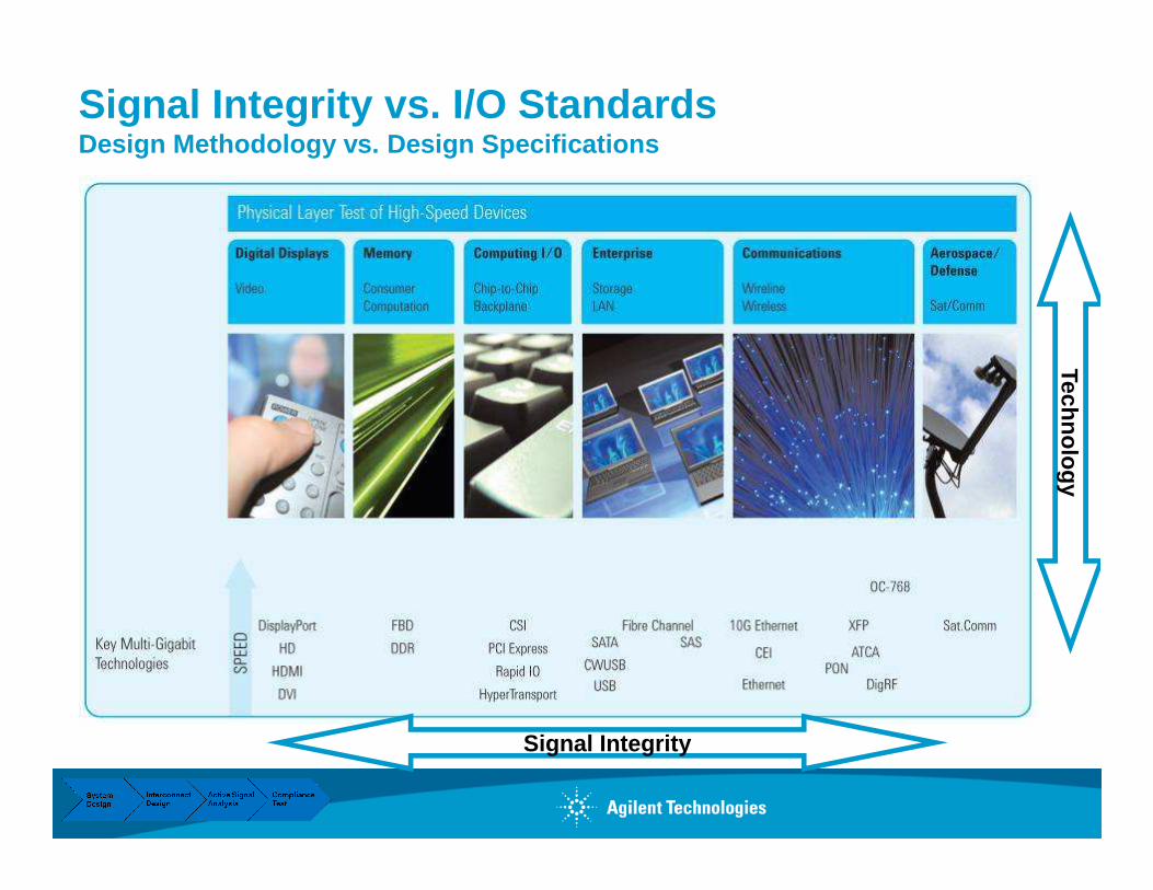
TechnologySignal Integrity vs. I/O StandardsDesign Methodology vs. Design Specifications
Technology
Signal Integrity

Agilent Digital Standards Program
Our solutions are driven and supported by Agilent experts involved in
international standards committees:
• Joint Electronic Devices Engineering Council (JEDEC)
• PCI Special Interest Group (PCI-SIG®)
• Video Electronics Standards Association (VESA)
• Serial ATA International Organization (SATA-IO)
• USB-Implementers Forum (USB-IF)
Page 48
We’re active in standards meetings, workshops, plugfests, and
seminars
• Mobile Industry Processor Interface (MIPI) Alliance
• Optical Internetworking Forum (OIF)
Our customers test with highest confidence and achieve compliance
faster
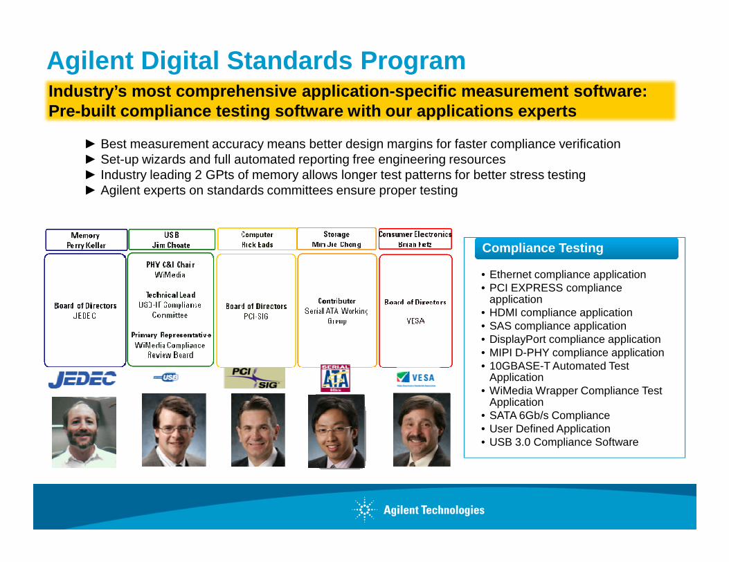
Industry’s most comprehensive application-specific measurement software: Pre-built compliance testing software with our appl ications experts
Agilent Digital Standards Program
► Best measurement accuracy means better design margins for faster compliance verification ► Set-up wizards and full automated reporting free engineering resources► Industry leading 2 GPts of memory allows longer test patterns for better stress testing► Agilent experts on standards committees ensure proper testing
• Ethernet compliance application
Compliance TestingCompliance Testing
• PCI EXPRESS compliance application
• HDMI compliance application • SAS compliance application • DisplayPort compliance application • MIPI D-PHY compliance application • 10GBASE-T Automated Test
Application • WiMedia Wrapper Compliance Test
Application • SATA 6Gb/s Compliance • User Defined Application • USB 3.0 Compliance Software
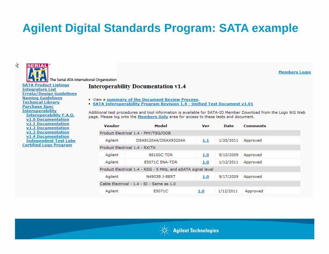
Agilent Digital Standards Program: SATA example
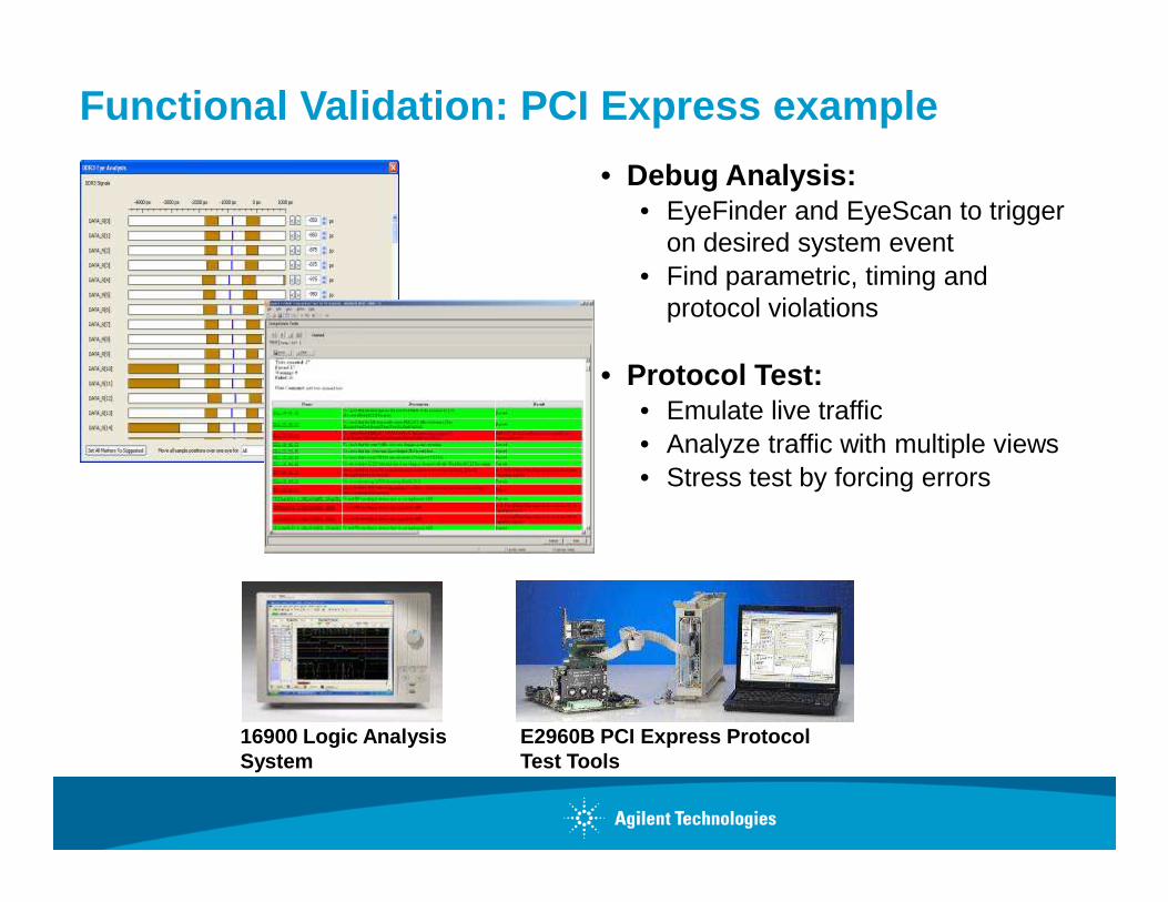
Functional Validation: PCI Express example
• Debug Analysis:• EyeFinder and EyeScan to trigger
on desired system event• Find parametric, timing and
protocol violations
• Protocol Test:• Emulate live traffic• Analyze traffic with multiple views• Analyze traffic with multiple views• Stress test by forcing errors
16900 Logic Analysis System
E2960B PCI Express Protocol Test Tools

Page 52
Questions?