1342 ieee transactions on microwave theory and …
TRANSCRIPT

1342 IEEE TRANSACTIONS ON MICROWAVE THEORY AND TECHNIQUES, VOL. 60, NO. 5, MAY 2012
Millimeter-Wave Self-Healing Power Amplifier WithAdaptive Amplitude and Phase Linearization
in 65-nm CMOSJenny Yi-Chun Liu, Student Member, IEEE, Roc Berenguer, Member, IEEE, and
Mau-Chung Frank Chang, Fellow, IEEE
Abstract—A self-healing two-stage millimeter-wave broadbandpower amplifier (PA) with on-chip amplitude/phase compensationis realized in 65-nm CMOS. The amplitude and phase com-pensations are accomplished by using feedback bias/capacitiveschemes to extend the linear operation region and optimize the PAefficiency. Tunable control knobs are inserted in the linearizationblock to enhance the PA performance yield against process/tem-perature variations and device ageing effects. This prototypeshows a 5.5-dB improvement of the output 1-dB compressionpoint and a less than 2% chip-to-chip gain variation.At a 1-V supply, the differential PA achieves a saturation outputpower of 14.85 dBm with a peak power-added-efficiency(PAE) of 16.2%. With the amplitude compensation, isincreased to 13.7 dBm. With the phase compensation, the outputphase variation is decreased to less than 0.5°. To the best of ourknowledge, this prototype provides the highest andwith simultaneously high PAE from a single PA reported to date.The PA delivers a linear gain of 9.7 dB and has a 7-GHz 3-dBbandwidth from 55.5 to 62.5 GHz with a compact total area of0.042 mm .
Index Terms—CMOS, millimeter-wave integrated circuits,power amplifier (PA), transformers, -band.
I. INTRODUCTION
O VER THE past decade, the emerging demands forhigh-data-rate (multi-Gb/s), short-range wireless com-
munications have led to dramatic progress in the developmentof low-cost millimeter-wave wireless systems [1], [2]. With itsappealing characteristics, such as broad bandwidth and securechannel reusability, the unlicensed spectrum around 60 GHzis ideal to support the multi-Gb/s wireless link applications,
Manuscript received September 28, 2011; revised February 07, 2012;accepted February 09, 2012. Date of publication April 03, 2012; date ofcurrent version April 27, 2012. This work was supported in part by the De-fense Advanced Research Projects Agency (DARPA)/U.S. Navy under GrantN66001-09-1-2030. This paper is an expanded paper from the IEEE RFICSymposium, June 5–10, 2011, Baltimore, MD.J. Y.-C. Liu was with the Department of Electrical Engineering, University of
California at Los Angeles (UCLA), Los Angeles, CA 90095 USA. She is nowwith the Department of Electrical Engineering, National Tsing Hua University,Hsinchu 300, Taiwan (e-mail: [email protected]).R. Berenguer is with the Electronic Engineering Department, Technological
Campus of University of Navarra (TECNUN), 20018 San Sebastian, Spain, andalso with the Communications Integrated Circuit Design Group (COMMIC),Centro de Estudio e Investigaciones Técnicas (CEIT), 20018 San Sebastian,Spain.M.-C. F. Chang is with the Department of Electrical Engineering, University
of California at Los Angeles (UCLA), Los Angeles, CA 90095 USA.Color versions of one or more of the figures in this paper are available online
at http://ieeexplore.ieee.org.Digital Object Identifier 10.1109/TMTT.2012.2189119
Fig. 1. Output power and PAE of recent reported -band PAs.
such as high-definition video streaming and high-speed datatransfer. In order to achieve high data rate, complex digitalmodulation schemes are usually used, which require a highlylinear transmitter to minimize both error vector magnitude(EVM) and spectral regrowth. The power amplifier (PA)greatly affects the output signal quality and the overall effi-ciency and remains one of the most challenging blocks in aCMOS transceiver. The recently reported millimeter-wave PAsmainly focus on delivering high output power and providinghigh power gain by techniques such as power combining, neu-tralization, and low-loss passive design in CMOS [3]–[12], andnovel stacked-transistor structure in metamorphic HEMTs [13].Notwithstanding the advantages of low-cost and high-levelintegration capability, the nonlinear transconductance and tem-perature-dependent mobility of the deep-scaled CMOS processoften result in early gain compression in PAs. This leads toa soft gain profile that has a large setback of the output 1-dBcompression point from the saturation output power
and that severely limits the linear operating range undera constrained supply voltage. To maintain the required linearityperformance, the PA commonly operates at the power back-offfrom . However, the output power and the efficiency rolloff rapidly in the power back-off region. Fig. 1 shows the effi-ciency for a collection of -band PAs at its peak output powerand at 1-, 3-, and 6-dB power back-off regions. The efficiencydrops below 10% when the PA is at the 3-dB back-off. Poorefficiency in the power back-off region results in a short batterylife for portable devices.To enhance the available linear output power and the av-
erage operating efficiency, a linearization/efficiency enhance-ment technique is necessary. However, common linearizationtechniques encounter practical design difficulties at millimeter-
0018-9480/$31.00 © 2012 IEEE

LIU et al.: MILLIMETER-WAVE SELF-HEALING PA 1343
Fig. 2. Self-healing transmitter block diagram.
wave frequencies at wide signal bandwidth and amplitude/phasepath mismatches [14]. Moreover, most of the approaches re-quire complicated auxiliary circuitries, such as a high-efficiencydc-to-dc converter and digital calibration that consume extrapower and silicon area.In addition to the above-mentioned issues, there are addi-
tional design challenges coming from CMOS technology toa PA design. The challenges arise from the low breakdownvoltage, the conductive substrate, and the high sheet resis-tance of the polysilicon that limit the output power, efficiency,linearity, and gain of the PA. As the device feature size con-tinues to scale down, process variations become significantand deteriorate the design-for-manufacturability (DFM) ofhigh-performance PAs. In deep-scaled CMOS technology, theissues of performance yield and device ageing have becomeas important as the circuit performance itself. In recent years,self-healing low-noise amplifiers (LNAs) have been proposed.Novel calibration methods are presented to maintain the inputmatch at 1.9 GHz with the need of an external RF signal source[15] and to improve LNA performance yield at 875 MHz basedon oscillation principles [16], [17].In this paper, the first self-healing linear CMOS PA in the
60-GHz unlicensed band is presented. This is the first CMOSmillimeter-wave PA integrated with on-chip amplitude andphase compensations to effectively enhance the linearity andthe back-off efficiency of the PA, which makes it suitable for thehigh data-rate wireless digital communications. By a built-indynamic feedback bias control scheme, the is extended by5.5 dB to fully utilize the limited supply voltage to maximizethe linear power region, thus increasing the transmitted powerwhile satisfying the spectrum and constellation requirements 0.Compared with the conventional feedback schemes, the pro-posed feedback presents a simple linearization method that canbe easily embedded to the PA. A phase-compensation techniqueis applied to overcome the phase variation when power varies.In the compensation blocks, low-overhead tunable knobs areproposed to self-heal the performance in response to processand environmental variations. Fig. 2 shows that the proposedPA can be integrated with a conventional transmitter, detectors,a self-healing controller (SHC), and a baseband processor toenable a self-healing transmitter [19]. With the self-healingloop, the output profile of the PA is tunable and can be used
Fig. 3. Circuit schematic of the PA.
to compensate the compressive gain profile of the previousstages in a conventional transmitter. It can be further used toovercome any variations that cause gain deviation and resultsin an overall flat gain over the output power that is desirablein modern wireless communication systems with complexdigital modulation schemes. The tunable knobs improve theperformance yield to achieve an average of 2% chip-to-chipgain variation of the PA. This unique aspect of PA design hasnot been discussed or implemented in prior arts. This prototypeoccupies an area of 0.47 mm 0.76 mm and is implementedin 65-nm CMOS technology.This paper is organized as follows. Section II describes the
design details of the baseline PA and the proposed compensationcircuits. Section III presents the concept of the self-healing algo-rithm. The measurement results of the 65-nm PA prototype arepresented in Section IV followed by a conclusion in Section V.
II. SELF-HEALING PA DESIGN
This section presents the design of the PA in 65-nm 1P6Mstandard CMOS technology with the emphasis on the proposedamplitude and phase compensation techniques to linearize thePA.
A. Baseline PA Design
A two-stage PA is designed to simultaneously optimizeoutput power, efficiency, and linearity at all power levelswhile maintaining a compact size. This PA is a differentialtransformer-coupled design. The circuit schematic is shown inFig. 3. This 65-nm CMOS process offers six metal layers withone thick top metal for low-loss passive design and intercon-nects. The unity current gain frequency and unity powergain frequency of the devices are higher than 180 and200 GHz, respectively. The gate lengths of all amplifier devicesare 60 nm to minimize the channel transit time.Both stages of the PA are designed with the common source
topology to maximize voltage headroom under a limited powersupply. In order to deliver a large output power, the output stageof the PA must have a sufficiently large device periphery. Sizecannot be excessively large because of the large parasitics asso-ciated with it that introduce extra loss. Furthermore, it impliesa low inductance is needed for the load. This can be achievedby reducing the coil width or the coil diameter. However, bothmethods have limitations in physical implementation. The am-plifier is designed in a way that the first stage saturates later than

1344 IEEE TRANSACTIONS ON MICROWAVE THEORY AND TECHNIQUES, VOL. 60, NO. 5, MAY 2012
the last stage, and therefore does not limit the overall . Theinput-referred of the first stage is approximately 3.5 dBlarger than the input-referred of the output stage. There-fore, the maximum linear power is dominated by the last stage.The transistor sizes of the two stages are 80 m and120 m with a finger width of 1 and 1.2 m, respec-tively. A finger width around 1 m in advanced technologypresents a good compromise between power gain and outputpower [20]. A large finger width results in a high gate resis-tance that decreases . A large number of fingers compli-cates the routing interconnects in a device layout that introduceextra losses and decrease gain. A finger width of 1.2 m insteadof 1 m in the last stage provides a layout with smaller aspectratio that minimizes interconnect lengths.Differential configuration is chosen to minimize the interfer-
ences to other blocks, lower the even-order harmonics, and re-ject the common-mode noise. The amplitude/phase mismatchesbetween the differential paths are within 0.5 dB and 1°, respec-tively, from small- to large-signal regions. These numbers arekept small because of the simple design and the careful per-formed symmetrical layout. The mismatches result in a gaindegradation of 0.2 dB. An RC network is added at the gates ofboth stages to stabilize the amplifier around 40 GHz without sig-nificantly degrading the power gain at 60 GHz. The amplifier isbiased at class-AB region to balance gain, power, and efficiency.This design utilizes transformers to provide a compact
impedance matching, improve the stability, and enable a simplebiasing scheme applied at the center taps. The high-passcharacteristic of the transformers ensures stability at lowfrequencies. At the input and output ports, the transformersachieve impedance matching and also convert single-endedsignals to differential ones and vice versa to simplify the testinginterface with single-ended instruments. These transformers aredesigned with the RF pads to match to a 50- load at 60 GHz.The loss of the input and output pads is around 0.8 dB. Thewidth of the input transformer is relatively narrow (4 m)to minimize the capacitive coupling from coils to substrate tomaximize the self-resonant frequency. Both the primary andsecondary coils are implemented on the top metal to maximizethe quality factors. The width of the inter-stage and outputtransformers ( and ) is wider (10 m) to provide lowinductances to match with large devices in the last stage and toprovide sufficient current-handling capability ( 100 mA). Dueto their large sizes, vertically stacked transformers are adoptedfor a compact design. Stabilizing resistors are inserted at thecenter taps of the transformers to improve the common-modestability. Since the device characteristics are highly layout-de-pendent, transistors, interconnects, and passive componentsare modeled in a full-wave electromagnetic (EM) simulator tocharacterize the distributed effects.
B. Adaptive Biasing Scheme
To ensure the linearity performance is maintained in the en-tire dynamic range, the PA needs to be biased at a high quiescentpoint to provide linear operation in the high power region. How-ever, it is not power efficient to maintain the high bias condition
Fig. 4. Concept of the adaptive biasing scheme.
when the transmitted power is low. In general, a communica-tion system works at its peak power level in less than 10% ofits total operation period. The PA wastes a significant amountof power if the biasing current is high. To simultaneously opti-mize the power-added efficiency (PAE) and linearity across thewhole dynamic range, Fig. 4 shows a simple adaptive biasingscheme. The dynamic bias control unit tracks the output swingof the PA and adjusts the bias of the PA accordingly.The proposed bias scheme along with the PA schematic is
shown in Fig. 3. In order to maximize the linear operating powerrange and improve the back-off efficiency, a novel feedback biascontrol loop ( – , , , and ) is applied to the laststage to dynamically adjust its gate bias according to theoutput power level.This amplitude compensation circuitry presents small area
(0.5%) and power (1%) overheads. Low-threshold pMOS de-vices ( , ) are connected to the last stage as an envelopedetector to sense the differential output voltage. These two tran-sistors have a negligible effect on the PA performance due totheir small loading imposed on the PA. Depending on the sensedoutput voltage swing, the feedback loop adjusts the gate bias ofthe last stage ( , ) in real time. The optimal curve isfirst acquired from simulation to minimize dc power consump-tion in the low power region and adaptively increase the gainwhile the power increases. The sizes of are selectedaccordingly so that the feedback bias matches the optimal onefrom simulation. A 1-pF capacitor is inserted to filter thehigh-frequency components. By properly selecting the param-eters of , , and , the bandwidth of the loop can be sethigher than that of the signal envelope. The bandwidth of theloop can be estimated by the following equations:
Bandwidth (1)
(2)
(3)
where and represent the total resistance and capac-itance at the node , respectively. Since is much largerthan the input capacitance of the output stage ,is dominated by . With a sufficient bandwidth, canpromptly track the input signal envelope. In this study, the 3-dBbandwidth of this feedback loop is 2 GHz, as shown in Fig. 5.Three voltage control knobs, , , and ,
shape the gain profile in three different aspects, as indicated inFig. 6. At low input power, the feedback transistors are off, and

LIU et al.: MILLIMETER-WAVE SELF-HEALING PA 1345
Fig. 5. Simulated voltage at the feedback node.
Fig. 6. Three control knobs vary the gain profile in three dimensions.
the gate voltage is set by and the resistor network (and ) at a low level to optimize efficiency
(4)
The linear gain is determined by . In this region, the gain ofthe PA can be modeled by the following equation:
(5)
where and are the empirical fitting coefficients. When theoutput power level is low, . As the output voltageswing becomes larger than the threshold voltage of the feed-back transistors, the feedback loop turns on and controls toextend the linear region
(6)
(7)
where and represent the total current and impedanceat the node , respectively, and can be expressed as follows:
(8)
(9)
The change of the gate bias, , is proportional to the currentfrom the feedback transistors ( , ), , which is determinedby the transistor aspect ratio and effective gate voltage
Fig. 7. Feedback gate bias of the last stage of the PA.
. The physical sizes of and set the range and the rateof change in the feedback bias . The feedback transistors arebiased near the threshold. The current can be expressed as [14]
(10)
(11)
where is the conduction angle and is the maximum cur-rent swing. pMOS transistor ( , ) is chosen over its nMOScounterpart for the envelope detection. It is because pMOS turnsoff when the output voltage swing is small and it turns on whenthe voltage swing increases. nMOS turns on regardless of theoutput voltage swing since the dc level of the gate terminals of
and are fixed to 1 V. Thus, using a pMOS transistorsaves dc power when the output power is low and simplifies thecontrol of the feedback voltage .Transistor acts as an enabler of the loop. Tuning the gate
voltage of adjusts the feedback factor that deter-mines the amount of the gain expansion Gain .controls the triggered power where the feedback action occursby changing the threshold voltage of the feedback transistors.As shown in Fig. 7, starts at 0.5 V in the small-signalregion and the gain of this feedback loop is small. grad-ually increases to 0.8 V as the PA is entering saturation re-gion. Since the amplitude compensation circuitry operates inthe large-signal region, the gain of the feedback loop changeswith the output power level of the PA. When output power in-creases from 6 to 14 dBm, the average gain of the loop is approx-imately 26 mV/dBm. In this region, the gain of the PA remains,and therefore, the linear operation region extends. After the PAreaches its saturation region, the gain starts to decrease. Unlikecommon feedback techniques used in the operational amplifiers,this feedback circuitry senses the RF signal and returns a signalat much lower frequency. This loop does not create any stabilityissues because the poles of the loop are far below 60 GHz. Aspart of the PA, the effects of process variation on the feedbackloop are overcome with the global self-healing process, as de-scribed in Section III.

1346 IEEE TRANSACTIONS ON MICROWAVE THEORY AND TECHNIQUES, VOL. 60, NO. 5, MAY 2012
Fig. 8. Simulated NMOS, PMOS, and total gate capacitances as a function ofgate–source voltage at a fixed V.
C. Phase Compensation
Besides amplitude distortion, phase distortion also affectssignal linearity in CMOS PAs. While amplitude distortion iswell understood, amplitude-to-phase conversion (AM-to-PM)has remained inscrutable and has not been discussed as muchin literature, despite its potentially disruptive effects on phasemodulated signals. In general, AM-to-PM conversion can betraced to the signal-dependent transistor parameters, such asthe input capacitance. Therefore, phase distortion is especiallysubstantial during the large-signal operation of PAs.In typical class-AB operation, the gate voltage changes ac-
cording to the input signal level and turns on and off the PA.The gate capacitance changes dramatically with the varying gatevoltage. Since the gate–drain capacitance is relatively in-sensitive to the gate voltage, the nonlinear input capacitance ismainly due to the gate–source capacitance . A PMOS-basedcapacitance compensation technique is applied by adding a par-allel pMOS transistor at the input of the PA to heal the phasedistortion [21]. Fig. 8 shows the individual of an nMOS tran-sistor, pMOS transistor, and the combined gate capacitance ofthe two as a function of the gate voltage at 60 GHz. It is clearthat the of the nMOS transistor increases abruptly whenchanges from 0.2 to 0.6 V, the class-AB operation region. Tocompensate this change, a pMOS transistor is inserted in par-allel with the nMOS transistor such that when the nMOS tran-sistor is off, the pMOS transistor turns on to maintain the samecapacitance at the input. Therefore, no matter which operationregion the PA is in, the input capacitance is approximately con-stant. By choosing the sizes and bias voltage of the pMOS tran-sistors ( , in Fig. 3), the of the pMOS transistor has acomplementary characteristic to the of the nMOS transistorto cancel the nonlinear behavior of the nMOS input capacitor.The variation of the total input capacitance of the outputstage is reduced from 140 to 45 fF. The pMOS transistors in-crease the total input capacitance. As is inverse proportionalto the gate capacitance, it decreases from 180 to 135 GHz withthe pMOS transistor. is more sensitive to the gate resis-tance than the gate capacitance, therefore, it decreases from 211to 186 GHz with the pMOS transistor. The effect of includingthe pMOS transistors is accounted for in this design by properlyselecting the transformer such that there is negligible gain orpower degradation.
Fig. 9. IQ constellation illustration.
Fig. 10. Simulated EVM with gain and phase deviations.
D. Linearity Effects of Amplitude and Phase Mismatches
The EVM, a common figure-of-merit to evaluate the digitallymodulated signal quality, is caused by both amplitude and phasedistortion of the signal, as shown in Fig. 9. Therefore, it can beestimated from the AM-to-AM and AM-to-PM characteristicsof the PA. The EVM is , where is the mag-nitude of the error between the ideal symbol and the distortedsymbol and A is the magnitude of the ideal symbol. The EVMcan be derived from the amplitude and phase deviations. As-suming the ideal and the distorted symbols have an amplitudeand phase of ( ) and , respectively.By trigonometric, a generalized EVM equation is shown as fol-lows:
100
(12)
where is assumed to be small and in degree in this approxi-mation. In this equation, represents the gain distortion andrepresents the phase distortion. It can be estimated from Fig. 10for maintaining an EVM of 20 dB or lower for 16 quadra-ture amplitude modulation (16-QAM), operation, should beapproximately within 0.95–1.05 and should be within 2°.In this design, we target the gain and phase variations within

LIU et al.: MILLIMETER-WAVE SELF-HEALING PA 1347
Fig. 11. Simulated EVM with and without the loop.
Fig. 12. Simulated constellation of the PA with a symbol rate of 2 GS/s.
0.5 dB and 1°, respectively, to assure an dB withat least 3-dB system margin.With the amplitude and phase linearization, the EVM of the
PA improves substantially as indicated in Agilent GoldenGate-based post-layout simulations, while modeling devices and in-terconnects as multiport components in an EM (Momentum)simulator. The EVM is greatly improved, as shown in Fig. 11,with both amplitude and phase compensation schemes. When
is 13 dBm, the EVM is drastically reduced from 11 to23 dB. Due to the amplitude compensation, the PA’s large-
signal gain has also been boosted to match its small-signal gainand rendered its much closer to . Fig. 12 shows thepost-layout simulated EVM to be 23 dB with output power of13 dBm for 16-QAM modulation at a symbol rate of 2 Giga-symbols/s.
III. SELF-HEALING ALGORITHM
In deep-scaled CMOS technology, process variation is thepredominant cause of chip-to-chip performance variations thatlimits the performance yield. The proposed PA in conjunctionwith an SHC, an envelope detector, and a power detector (not in-tegrated in this study) work to overcome the limitations imposedby process and environmental variations, as shown in Fig. 2.A calibration unit is embedded in the SHC to provide calibra-tion for absolute power and temperature. The self-healing unitis further integrated with a transceiver to monitor and diagnosethe key performances of the transceiver such as the noise figure
of the receiver and the linearity of the transmitter without ex-ternal testing instruments throughout the lifetime of the radio[19]. The self-healing unit includes a one- and two-tone ampli-tude-controllable test-pattern generator on the transmit side andan auxiliary ADC and 128-point fast Fourier transform (FFT)processor on the receive side to observe the received spectrumfrom the detectors. The output is passed to a parameter estimator(PE) for robust estimation. The radio is optimized subject to acost function [22]
where is the weighting of the th radio specification beingoptimized, is a vector of states in the radio, is a vector of theobserved outputs from the radio, and is a function thatmaps and to actual specifications. A larger weighting factoris applied to the specification that contributes more to the overallradio performance. With the embedded control knobs, the radiobecomes highly adjustable. The self-healing algorithm can op-timize multiple performances sequentially to meet a given costfunction. In the process of self-healing, the radio function istemporarily suspended.To heal the gain and power in the PA, the SHC first provides
the input test signals to the PA. The SHC then receives the dataprovided by the calibrated detectors at the PA output and returnsthree control knob signals, , , and , to thePA. By fine adjusting these knobs, the gain profile of the PAcan be effectively shaped to simultaneously overcome processvariations and gain compression to meet both the small- andlarge-signal specifications. Fig. 13 shows the self-healing flowof the PA. An off-chip well-calibrated power sensor is necessaryfor power measurements in this test chip. The proposed healingalgorithm is described as follows.1) A low-power reference signal is generated and sent intothe PA. By monitoring the calibrated output power fromthe power detector, the self-healing engine can resolve thelinear gain and optimize it by adjusting .
2) After the linear gain is healed, a power-sweep function isconducted to obtain and , as shownin Fig. 6. To avoid signal distortion and extend closeto , both values should be kept within a certainrange (e.g., 1 dB). can be adjusted to tune thelocation and the amount of the gain expansion. It shouldbe chosen such that Gain is less than 1 dB.
3) Once Gain is less than 1 dB, Gain is exam-ined. can be adjusted such that Gain is alsoless than 1 dB. At this point, the PA has self-healed itsgain and power. Since these knobs shape the gain profile inthree independent aspects, they can be adjusted one by onesequentially to optimize the performances of the PA. Thesimulated distributions before and after self-healingare shown in Fig. 14. Monte Carlo simulations in CadenceSpectre are performed in the typical corner (tt) and twoworse corners, slow-slow (ss) and fast-fast (ff) with de-vice mismatches. One hundred random runs are simulatedin each process corner. Before self-healing is applied, themean of the ss, ff, and tt corner is around 13.2, 13.85, and

1348 IEEE TRANSACTIONS ON MICROWAVE THEORY AND TECHNIQUES, VOL. 60, NO. 5, MAY 2012
Fig. 13. Flowchart of the self-healing algorithm for enhancing both PA perfor-mance and performance yield.
14.4 dBm, respectively. After the self-healing process isapplied, all samples under different process corners centeraround 14.4 dBm with a variation within 1 dBm. There-fore, the performance yield is largely improved. A similarhealing flow is applied to heal the transceiver.
IV. MEASUREMENT RESULTS
The PA prototype is fabricated in TSMC 65-nm CMOS tech-nology. The chip micrograph is shown in Fig. 15. The PA oc-cupies a compact area of 0.76 mm 0.47 mm including thepads with an active core area of 0.26 mm 0.16 mm. Thecompact area demonstrates the utility of the transformers at themillimeter-wave region. The amplitude compensation circuitryconsumes an area of 220 m , which is approximately 0.5% ofthe total core area. Small- and large-signal measurements areperformed. All measurements are done via on-chip probing.
A. Small-Signal Performance
The -parameters are tested from dc to 67 GHz using anAgilent 8731 E network analyzer calibrated by the Cascade
Fig. 14. Simulated distribution at different corners.
Fig. 15. Chip micrograph of the proposed PA.
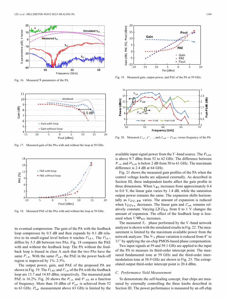
short-open-load-thru (SOLT) calibration substrate. The mea-sured -parameters with a 1-V supply are shown in Fig. 16with a peak linear gain of 9.7 dB at 59 GHz. The simulatedis shown in the same figure to demonstrate the close correlationbetween simulation and measurement. The 3-dB bandwidthis 7 GHz from 55.5 to 62.5 GHz. The input return loss, ,is greater than 20 dB from 52 to 67 GHz. The output returnloss, , is greater than 10 dB from 52 to 60 GHz. A stabilityfactor greater than 1 across the entire spectrum demonstratesunconditional stability.
B. Large-Signal Performance
Single-tone swept-signal performance of the PA is performedby an HP 83557 A -band sourcemodule and an Agilent V8486A -band power sensor. To show the effectiveness of the feed-back control loop, a PA without the loop is fabricated for com-parison. Fig. 17 shows the gain profiles of the PAs with andwithout the loop operated at a 1-V supply. The two PAs havethe same gate biases in the small-signal region. Therefore, bothPAs have the same linear gain. As the input power increases,the PA without the feedback loop starts to compress because ofthe limited maximum current, whereas the one with the loop re-mains relatively constant until it experiences expansion before
LIU et al.: MILLIMETER-WAVE SELF-HEALING PA 1349
Fig. 16. Measured -parameters of the PA.
Fig. 17. Measured gain of the PAs with and without the loop at 59 GHz.
Fig. 18. Measured PAE of the PAs with and without the loop at 59 GHz.
its eventual compression. The gain of the PA with the feedbackloop compresses by 0.5 dB and then expands by 0.1 dB rela-tive to its small-signal level before it reaches . Thediffers by 5.5 dB between two PAs. Fig. 18 compares the PAEwith and without the feedback loop. The PA without the feed-back loop is biased in class A such that the two PAs have thesame . With the same , the PAE in the power back-offregion is improved by 1%–2.5%.The output power, gain, and PAE of the proposed PA are
shown in Fig. 19. The and of the PAwith the feedbackloop are 13.7 and 14.85 dBm, respectively. The measured peakPAE is 16.2%. Fig. 20 shows the and as a functionof frequency. More than 10 dBm of is achieved from 52to 63 GHz. measurement above 63 GHz is limited by the
Fig. 19. Measured gain, output power, and PAE of the PA at 59 GHz.
Fig. 20. Measured , , and versus frequency of the PA.
available input signal power from the -band source. Theis above 9.7 dBm from 52 to 62 GHz. The difference between
and is below 2 dB from 50 to 61 GHz. The maximumdifference is 2.4 dB at 64 GHz.Fig. 21 shows the measured gain profiles of the PA when the
control voltage knobs are adjusted externally. As described inSection III, three independent knobs affect the gain profile inthree dimensions. When increases from approximately 0.4to 0.6 V, the linear gain varies by 1.4 dB, while the saturationoutput power remains the same. The expansion shifts horizon-tally as varies. The amount of expansion is reducedwhen decreases. The linear gain and remains rel-atively constant. Varying from 0 to 1 V changes theamount of expansion. The effect of the feedback loop is less-ened when increases.The measured phase performed by the -band network
analyzer is shownwith the simulated results in Fig. 22. Themea-surement is limited by the maximum available power from thenetwork analyzer. The phase variation is reduced from 4 to11 by applying the on-chip PMOS-based phase compensation.Two input signals at 59 and 59.1 GHz are applied to the input
of the PA to measure its third-order intercept point. The mea-sured fundamental tone at 59 GHz and the third-order inter-modulation tone at 58.9 GHz are shown in Fig. 23. The extrap-olated output third-order intercept point is 20.4 dBm.
C. Performance Yield Measurement
To demonstrate the self-healing concept, four chips are mea-sured by externally controlling the three knobs described inSection III. The power performance is measured by an off-chip

1350 IEEE TRANSACTIONS ON MICROWAVE THEORY AND TECHNIQUES, VOL. 60, NO. 5, MAY 2012
Fig. 21. Measured PA gain profiles when varying the three control knobs.
Fig. 22. Measured and simulated phase with and without phase compen-sation.
Fig. 23. Measured two-tone performance of the PA.
-band power sensor. The results are shown in Fig. 24. Beforeapplying the healing algorithm, the three control knobs are bi-ased at fixed voltages and the gain profiles show variations inboth small- and large-signal regions. After externally control-ling the three knobs, as described in Section III, the four chipsshow a gain variance of 2%, which is significantly reduced ascompared to 22% before healing.As shown in the self-healing transmitter block diagram in
Fig. 2, the PA prototype has been integrated in a superhetero-dyne transmitter, alongwith ADC, SHC, detectors, and the base-band processor to form a self-healing transmitter [19]. Withthe control knobs in the PA and the mixer, and the in-phase/quadrature (IQ) correction unit in the digital baseband, the trans-mitter becomes highly adjustable to reduce the performance de-viations. During the self-healing cycle, a two-tone test signalis applied to the transmitter and the output of the transmitteris detected by the envelope detector. A steepest descent algo-rithm is used to adjust the transmitter control knobs to minimize
Fig. 24. Measured gain with and without healing.
Fig. 25. Measured statistical distribution for ten chips of the transmitter third-order intermodulation before and after self-healing.
the output third-order intermodulation (OIM3) terms [22]. Themost sensitive knob is adjusted with the highest priority. Statis-tical OIM3 measurements of ten transmitter chips are shown inFig. 25. Before self-healing, the OIM3 levels of the ten trans-mitter chips are high (around 33 dBc) with a large variation.After self-healing, the OIM3 levels are reduced to be lower than40 dBc with a smaller variation. This satisfies the pre-speci-
fied transmitter OIM3 requirement of 40 dBc and assures a100% transmitter performance yield.

LIU et al.: MILLIMETER-WAVE SELF-HEALING PA 1351
TABLE ICOMPARISON OF 60-GHz SILICON PAs
FoM PAE mW mWIncluding padsEstimated from figures
Table I summarizes the performance of recently published-band CMOS PAs. Without a power-combining technique,
most of the PAs deliver lower than 13.8 dBm of output power,which is more than 1-dB less than this study. The highestof this study demonstrates the effectiveness of the proposed gainexpansion technique. The PAE at and power back-off aregreatly improved, as shown in Fig. 1. This study achieves thehighest figure-of-merit of 69.6 [defined by
] that compares favorably to the prior studies.
V. CONCLUSION
A -band CMOS PA with both local-level adaptive feed-back bias control and global-level self-healing control is de-signed and demonstrated in 65-nm CMOS. With the proposedcontrol/healing algorithm, the PA’s linear operation range hasbeen effectively extended by 5.5 dB. Test results indicate thatthe CMOS PA can deliver dBm and
dBm with 16.2% peak PAE. The performance mappingfrom multiple chips demonstrates effectiveness of both adap-tive feedback and self-healing control capabilities of the PA forimproving its performance and yield through on-chip perfor-mance detectors and current control knobs. The demonstratedhealing and control methodologies can help realize future gen-eration millimeter-wave radio-on-chips to be implemented indeep-scaled CMOS technologies for high data-rate communi-cations with both high performance and high yield.
ACKNOWLEDGMENT
The authors thank the Taiwan Semiconductor ManufacturingCompany (TSMC), Hsinchu, Taiwan, for foundry support andDr. N.-Y. Wang, Broadcom, Irvine, CA, Prof. J. Q. Gu, Uni-versity of Florida, Gainesville, Dr. Z. Xu, HRL Laboratories,Malibu, CA, Dr. C. Chien, CreoNex, Westlake Village, CA,and Dr. A. Tang, Jet Propulsion Laboratory, Pasadena, CA, fortechnical discussion. Chip fabrication was provided by TSMC.
REFERENCES[1] A. Tomkins, R. A. Aroca, T. Yamamoto, S. T. Nicolson, Y. Doi, and
S. P. Voinigescu, “A zero-IF 60 GHz 65 nm CMOS transceiver withdirect BPSK modulation demonstrating up to 6 Gb/s data rates overa 2 m wireless link,” IEEE J. Solid-State Circuits, vol. 44, no. 8, pp.2085–2099, Aug. 2009.
[2] S. Pinel, S. Sarkar, P. Sen, B. Perumana, D. Yeh, D. Dawn, and J.Laskar, “A 90 nm CMOS 60 GHz radio,” in IEEE Int. Solid-State Cir-cuits Dig., Feb. 2008, pp. 130–131.
[3] K. Raczkowski, S. Thijs, W. D. Raedt, B. Nauwelaers, and P.Wambacq, “50-to-67 GHz ESD-protected power amplifiers in digital45 nm LP CMOS,” in IEEE Int. Solid-State Circuits Dig., Feb. 2009,pp. 382–383.
[4] W. L. Chan, J. R. Long, M. Spirito, and J. J. Pekarik, “A 60 GHz-band1 V 11.5 dBm power amplifier with 11% PAE in 65 nm CMOS,” inIEEE Int. Solid-State Circuits Dig., Feb. 2009, pp. 380–381.
[5] N. Kurita and H. Kondoh, “60 GHz and 80 GHz wide band poweramplifier MMICs in 90 nm CMOS technology,” in IEEE Radio Freq.Integr. Circuits Symp., Jun. 2009, pp. 39–42.
[6] M. Bohsali and A. M. Niknejad, “Current combining 60 GHz CMOSpower amplifiers,” in IEEE Radio Freq. Integr. Circuits Symp., Jun.2009, pp. 31–34.
[7] T. Quemerais, L. Moquillon, V. Huard, J.-M. Fournier, P. Benech, andN. Corrao, “DC hot carrier stress effect on CMOS 65 nm 60 GHz poweramplifiers,” in IEEE Radio Freq. Integr. Circuits Symp., Jun. 2010, pp.351–354.
[8] S. Aloui, E. Kerherve, R. Plana, and D. Belot, “RF-pad, transmissionlines and balun optimization for 60 GHz 65 nm CMOS power am-plifier,” in IEEE Radio Freq. Integr. Circuits Symp., Jun. 2010, pp.211–214.
[9] B. Martineau, V. Lnopik, A. Siligaris, F. Gianesello, and D. Belot, “A53-to-68 GHz 18 dBmpower amplifier with an 8-way combiner in stan-dard 65 nm CMOS,” IEEE Int. Solid-State Circuits Dig., pp. 428–429,Feb. 2010.
[10] M. Boers, “A 60 GHz transformer coupled amplifier in 65 nm digitalCMOS,” in IEEE Radio Freq. Integr. Circuits Symp., Jun. 2010, pp.343–346.
[11] J.-W. Lai and A. V. Garcia, “A 1 V 17.9 dBm 60 GHz power amplifierin standard 65 nm CMOS,” in IEEE Int. Solid-State Circuits Dig., Feb.2010, pp. 424–425.
[12] J. Chen and A. M. Niknejad, “A compact 1 V 18.6 dBm 60 GHz poweramplifier in 65 nm CMOS,” in IEEE Int. Solid-State Circuits Dig., Feb.2011, pp. 432–433.
[13] Y. Kim, Y. Koh, J. Kim, S. Lee, J. Jeong, K. Seo, and Y. Kwon, “A60 GHz broadband stacked FET power amplifier using 130 nm meta-morphic HEMTs,” IEEE Microw. Wireless Compon. Lett., vol. 21, no.6, pp. 323–325, Jun. 2011.
[14] S. C. Cripps, RF Power Amplifiers for Wireless Communications.Norwood, MA: Artech House, 1999.
[15] T. Das, A. Gopalan, C. Washburn, and P. R. Mukund, “Self-calibrationof input-match in RF front-end circuitry,” IEEE Trans. Circuits Syst.,vol. 52, no. 12, pp. 821–825, Dec. 2005.

1352 IEEE TRANSACTIONS ON MICROWAVE THEORY AND TECHNIQUES, VOL. 60, NO. 5, MAY 2012
[16] A. Goyal, M. Swaminathan, and A. Chatterjee, “A novel self-healingmethodology for RF amplifier circuits based on oscillation principles,”in IEEE Design, Automat., Test Eur., Apr. 2009, pp. 1656–1661.
[17] A. Goyal, M. Swaminathan, A. Chatterjee, D. Howard, and J. D.Cressler, “A new self-healing methodology for RF amplifier circuitsbased on oscillation principles,” IEEE Trans. Very Large Scale Inte-gration (VLSI) Syst., to be published.
[18] J. Y.-C. Liu, A. Tang, N.-Y.Wang, Q. J. Gu, R. Berenguer, H.-H. Hsieh,P.-Y. Wu, C. Jou, and M.-C. F. Chang, “A -band self-healing poweramplifier with adaptive feedback bias control in 65 nm CMOS,” inIEEE Radio Freq. Integr. Circuits Symp., Jun. 2010, pp. 423–426.
[19] A. Tang, F. Hsiao, D. Murphy, I.-N. Ku, J. Y.-C. Liu, N.-Y. Wang, S.D’Souza, H. Wu, Y.-H. Wang, Y.-C. Kuan, M. Tang, M. Pham, G. Vir-bila, D. Yang, Q. Gu, C. Chien, and M.-C. F. Chang, “A low overheadself-healing embedded system for ensuring high performance yield andlong-term sustainability of a 60 GHz 4 Gbps radio-on-a-chip,” in IEEEInt. Solid-State Circuits Dig., 2012, pp. 316–317.
[20] T. Yao, M. Q. Gordon, K. K. W. Tang, K. H. K. Yau, M.-T. Yang, P.Schvan, and S. P. Voinigescu, “Algorithmic design of CMOS LNAsand PAs for 60-GHz radio,” IEEE J. Solid-State Circuits, vol. 42, no.5, pp. 1044–1057, May 2007.
[21] C. Wang, M. Vaidyanathan, and L. E. Larson, “A capacitance compen-sation technique for improved linearity in CMOS class-AB power am-plifiers,” IEEE J. Solid-State Circuits, vol. 39, no. 11, pp. 1927–1937,Nov. 2004.
[22] M.-C. F. Chang, C. Chien, A. Tang, and Q. J. Gu, “Self-healing 4 giga-bit/sec reconfigurable CMOS radio-on-a-chip,” in Government Micro-circuit Appl. Critical Technol. Conf., Mar. 2011, pp. 57–60.
Jenny Yi-Chun Liu (S’09) received the B.S. degreein electronics engineering from National Chiao TungUniversity, Hsinchu, Taiwan, in 2005, and the M.S.and Ph.D. degrees in electrical engineering from theUniversity of California at Los Angeles (UCLA), in2008 and 2011, respectively.In 2009, she was an Intern with the Taiwan
Semiconductor Manufacturing Company (TSMC),Hsinchu, Taiwan, where she designed RF/mil-limeter-wave front-end circuits. From 2011 to 2012,she was a Postdoctoral Scholar with UCLA. In
2012, she joined the Department of Electrical Engineering, National Tsing HuaUniversity, Hsinchu, Taiwan, as an Assistant Professor. Her current researchinterests include millimeter-wave and terahertz devices, circuits, and systems.Dr. Liu was the recipient of the Outstanding Contribution Prize of the 2010
Asia–PacificMicrowave Conference. She was also the recipient of the four-yearElite Fellowship for doctoral study of the National Science Council, Taiwan(2005–2009).
Roc Berenguer (M’05) received theM.Sc. and Ph.D.degrees from the Technological Campus of the Uni-versity of Navarra (TECNUN), San Sebastian, Spain,in 1996 and 2000, respectively.He is currently a Senior RF Researcher with the
Communications Integrated Circuits (COMMIC)Design Group, Centro de Estudio e InvestigacionesTécnicas (CEIT), San Sebastian, Spain, and anAssociate Professor with the Electrical, Electronic,and Control Engineering Department, TECNUN.In 1999, he joined the CEIT, as an Associated
Researcher. Through CEIT and INCIDE (spin-off of the COMMIC Group,CEIT), he has been an external consultant for Siemens, Munich, Germany(2000), Hitachi Microsystems Europe, Maidenhead, U.K. (2001), Xignal Tech-nologies, Munich, Germany (2001–2002), and Seiko-Epson, Barcelona, Spain(2006–2007), where he collaborated in the design of several RF front-endsfor wireless standards like GSM-EDGE, DAB, Wibree, etc. In 2009, he was
a Visiting Researcher with the Illinois Institute of Technology (IIT), Chicago,where he was involved in the design of a 77-GHz receiver front-end in 65-nmCMOS for a frequency-modulated continuous-wave (FM-CW) automotiveradar. During the 2010 summer semester, he was a Visiting Scholar with theUniversity of California at Los Angeles (UCLA), where he was involved withthe design optimization of a 60-GHz PA in 65-nm CMOS. He has authoredor coauthored two books, 20 international journals papers, and over 30 con-ference papers. He holds seven patents. His technical expertise and researchinterests are in the areas of CMOS RF/millimeter-wave integrated circuit (IC)design, ultra-low power analog circuit design for batteryless sensor nodes, andhigh-speed signal processing.
Mau-Chung Frank Chang (F’96) received the B.S.degree in physics from National Taiwan University,Taipei, Taiwan, in 1972, the M.S. degree in mate-rials science from National Tsing Hua University,Hsinchu, Taiwan, in 1974, and the Ph.D. degree inelectronics engineering from National Chiao TungUniversity, Hsinchu, Taiwan, in 1979.He is currently the Wintek Endowed Chair and
Distinguished Professor of Electrical Engineeringand the Chairman of the Electrical EngineeringDepartment, University of California at Los An-
geles (UCLA). Prior to joining UCLA, he was the Assistant Director andDepartment Manager of the High Speed Electronics Laboratory, RockwellScience Center (1983–1997), Thousand Oaks, CA. During this tenure, hedeveloped and transferred the AlGaAs/GaAs heterojunction bipolar transistor(HBT) and BiFET (planar HBT/MESFET) integrated-circuit technologies fromthe research laboratory to the production line (now Conexant Systems andSkyworks). The HBT/BiFET productions have grown into multibillion-dollarbusinesses and dominated the cell-phone PAs and front-end module markets(currently exceeding one-billion units/year). He was the Principal Investigatorwith Rockwell Science Center in leading the Defense Advanced ResearchProjects Agency (DARPA)’s ultrahigh-speed ADC/DAC development fordirect conversion transceiver (DCT) and digital radar receiver (DRR) systems.He was the inventor of the multiband reconfigurable RF interconnects based onFDMA and CDMA multiple access algorithms for chipmulti-processor (CMP)inter-core communications and inter-chip CPU-to-memory communications.He also pioneered the development of the world’s first multigigabit/s ADCs,DACs, and DDSs in both GaAs HBT and Si CMOS technologies, the first60-GHz radio transceiver front-end based on transformer-folded-cascode(Origami) high-linearity circuit topology, and the low phase-noise CMOSVCO dBc/Hz with digitally controlled on-chip artificialdielectric (DiCAD). He was also the first to demonstrate CMOS oscillatorsin the terahertz frequency spectrum (1.3 THz) and the first to demonstrate aCMOS active imager at the sub-millimeter-wave spectra (180 GHz) based ona time-encoded digital regenerative receiver. He was also the founder of theRF design company G-Plus (now SST and Microchip), which commercializesWiFi 11 b/g/a/n PAs, front-end modules, and CMOS transceivers. Throughouthis career, his research has primarily focused on the development of high-speedsemiconductor devices and integrated circuits for RF and mixed-signal com-munication and imaging system applications.Dr. Chang was elected to the U.S. National Academy of Engineering in 2008
for the development and commercialization of GaAs PAs and integrated circuits.He was the recipient of the 2006 IEEE David Sarnoff Award for the develop-ment and commercialization of HBT PAs for modern wireless communicationsystems, the 2008 Pan Wen Yuan Foundation Award, and the 2009 CESASCCareer Achievement Award for his fundamental contributions in developingAlGaAs/GaAs heterojunction bipolar transistors. His recent paper “CMP Net-work-on-chip Overlaid with Multiband RF-Interconnect” was selected for theBest Paper Award of the 2008 IEEE International Symposium on High-Perfor-mance Computer Architecture (HPCA). He was also the recipient of the 1992Rockwell Leonardo Da Vinci Award (Engineer of the Year), the 1997 NationalChiao Tung University Distinguished Alumnus Award, and the 2002 NationalTsing Hua University Distinguished Engineering Alumnus Award.