16-megabit 2.5-volt or 2.7-volt - sparkfun electronics · 16-megabit 2.5-volt or 2.7-volt dataflash...
TRANSCRIPT

16-megabit2.5-volt or2.7-voltDataFlash®
AT45DB161D
3500H–DFLASH–09/06
Features• Single 2.5V - 3.6V or 2.7V - 3.6V Supply• RapidS™ Serial Interface: 66 MHz Maximum Clock Frequency
– SPI Compatible Modes 0 and 3• User Configurable Page Size
– 512 Bytes per Page– 528 Bytes per Page
• Page Program Operation– Intelligent Programming Operation– 4,096 Pages (512/528 Bytes/Page) Main Memory
• Flexible Erase Options– Page Erase (512 Bytes) – Block Erase (4 Kbytes) – Sector Erase (128 Kbytes) – Chip Erase (16 Mbits)
• Two SRAM Data Buffers (512/528 Bytes) – Allows Receiving of Data while Reprogramming the Flash Array
• Continuous Read Capability through Entire Array– Ideal for Code Shadowing Applications
• Low-power Dissipation– 7 mA Active Read Current Typical– 25 µA Standby Current Typical – 9 µA Deep Power Down Typical
• Hardware and Software Data Protection Features – Individual Sector
• Sector Lockdown for Secure Code and Data Storage– Individual Sector
• Security: 128-byte Security Register– 64-byte User Programmable Space– Unique 64-byte Device Identifier
• JEDEC Standard Manufacturer and Device ID Read• 100,000 Program/Erase Cycles Per Page Minimum• Data Retention – 20 Years• Industrial Temperature Range• Green (Pb/Halide-free/RoHS Compliant) Packaging Options
1. DescriptionThe AT45DB161D is a 2.5-volt or 2.7-volt, serial-interface sequential access Flashmemory ideally suited for a wide variety of digital voice-, image-, program code- anddata-storage applications. The AT45DB161D supports RapidS serial interface forapplications requiring very high speed operations. RapidS serial interface is SPI com-patible for frequencies up to 66 MHz. Its 17,301,504 bits of memory are organized as4,096 pages of 512 bytes or 528 bytes each. In addition to the main memory, theAT45DB161D also contains two SRAM buffers of 512/528 bytes each. The buffersallow the receiving of data while a page in the main Memory is being reprogrammed,as well as writing a continuous data stream. EEPROM emulation (bit or byte alterabil-ity) is easily handled with a self-contained three step read-modify-write operation.Unlike conventional Flash memories that are accessed randomly with multiple

address lines and a parallel interface, the DataFlash uses a RapidS serial interface to sequen-tially access its data. The simple sequential access dramatically reduces active pin count,facilitates hardware layout, increases system reliability, minimizes switching noise, and reducespackage size. The device is optimized for use in many commercial and industrial applicationswhere high-density, low-pin count, low-voltage and low-power are essential.
To allow for simple in-system reprogrammability, the AT45DB161D does not require high inputvoltages for programming. The device operates from a single power supply, 2.5V to 3.6V or 2.7Vto 3.6V, for both the program and read operations. The AT45DB161D is enabled through thechip select pin (CS) and accessed via a three-wire interface consisting of the Serial Input (SI),Serial Output (SO), and the Serial Clock (SCK).
All programming and erase cycles are self-timed.
2. Pin Configurations and Pinouts
Figure 2-1. TSOP Top View: Type 1 Figure 2-2. DataFlash Card(1) Top View through Package
Note: 1. See AT45DCB002D Datasheet.
Figure 2-3. MLF Top View Figure 2-4. SOIC Top View
1234567891011121314
2827262524232221201918171615
RDY/BUSYRESET
WPNCNC
VCCGND
NCNCNCCS
SCKSI
SO
NCNCNCNCNCNCNCNCNCNCNCNCNCNC
7 6 5 4 3 2 1
SISCK
RESETCS
SOGNDVCCWP
8
7
6
5
1
2
3
4
1234
8765
SISCK
RESETCS
SOGNDVCCWP
23500H–DFLASH–09/06
AT45DB161D

AT45DB161D
Table 2-1. Pin Configurations
Symbol Name and FunctionAsserted
State Type
CS
Chip Select: Asserting the CS pin selects the device. When the CS pin is deasserted, the device will be deselected and normally be placed in the standby mode (not Deep Power-Down mode), and the output pin (SO) will be in a high-impedance state. When the device is deselected, data will not be accepted on the input pin (SI).A high-to-low transition on the CS pin is required to start an operation, and a low-to-high transition is required to end an operation. When ending an internally self-timed operation such as a program or erase cycle, the device will not enter the standby mode until the completion of the operation.
Low Input
SCK
Serial Clock: This pin is used to provide a clock to the device and is used to control the flow of data to and from the device. Command, address, and input data present on the SI pin is always latched on the rising edge of SCK, while output data on the SO pin is always clocked out on the falling edge of SCK.
– Input
SISerial Input: The SI pin is used to shift data into the device. The SI pin is used for all data input including command and address sequences. Data on the SI pin is always latched on the rising edge of SCK. If the SER/BYTE pin is always driven low, the SI pin should be a “no connect”.
– Input
SOSerial Output: The SO pin is used to shift data out from the device. Data on the SO pin is always clocked out on the falling edge of SCK. If the SER/BYTE pin is always driven low, the SO pin should be a “no connect”.
– Output
WP
Write Protect: When the WP pin is asserted, all sectors specified for protection by the Sector Protection Register will be protected against program and erase operations regardless of whether the Enable Sector Protection command has been issued or not. The WP pin functions independently of the software controlled protection method. After the WP pin goes low, the content of the Sector Protection Register cannot be modified.If a program or erase command is issued to the device while the WP pin is asserted, the device will simply ignore the command and perform no operation. The device will return to the idle state once the CS pin has been deasserted. The Enable Sector Protection command and Sector Lockdown command, however, will be recognized by the device when the WP pin is asserted.
The WP pin is internally pulled-high and may be left floating if hardware controlled protection will not be used. However, it is recommended that the WP pin also be externally connected to VCC whenever possible.
Low Input
RESET
Reset: A low state on the reset pin (RESET) will terminate the operation in progress and reset the internal state machine to an idle state. The device will remain in the reset condition as long as a low level is present on the RESET pin. Normal operation can resume once the RESET pin is brought back to a high level.
The device incorporates an internal power-on reset circuit, so there are no restrictions on the RESET pin during power-on sequences. If this pin and feature are not utilized it is recommended that the RESET pin be driven high externally.
Low Input
RDY/BUSY
Ready/Busy: This open drain output pin will be driven low when the device is busy in an internally self-timed operation. This pin, which is normally in a high state (through an external pull-up resistor), will be pulled low during programming/erase operations, compare operations, and page-to-buffer transfers.
The busy status indicates that the Flash memory array and one of the buffers cannot be accessed; read and write operations to the other buffer can still be performed.
– Output
VCCDevice Power Supply: The VCC pin is used to supply the source voltage to the device.
Operations at invalid VCC voltages may produce spurious results and should not be attempted.– Power
GNDGround: The ground reference for the power supply. GND should be connected to the system ground.
– Ground
33500H–DFLASH–09/06

3. Block Diagram
4. Memory ArrayTo provide optimal flexibility, the memory array of the AT45DB161D is divided into three levels of granularity comprising ofsectors, blocks, and pages. The “Memory Architecture Diagram” illustrates the breakdown of each level and details thenumber of pages per sector and block. All program operations to the DataFlash occur on a page by page basis. The eraseoperations can be performed at the chip, sector, block or page level.
Figure 4-1. Memory Architecture Diagram
FLASH MEMORY ARRAY
PAGE (512/528 BYTES)
BUFFER 2 (512/528 BYTES)BUFFER 1 (512/528 BYTES)
I/O INTERFACE
SCKCS
RESETVCCGND
RDY/BUSY
WP
SOSI
SECTOR 0a = 8 Pages4,096/4,224 bytes
SECTOR 0b = 248 Pages126,976/130,944 bytes
Block = 4,096/4,224 bytes
8 PagesSECTOR 0
SE
CTO
R 1
Page = 512/528 bytes
PAGE 0
PAGE 1
PAGE 6
PAGE 7
PAGE 8
PAGE 9
PAGE 4,094
PAGE 4,095
BL
OC
K 0
PAGE 14
PAGE 15
PAGE 16
PAGE 17
PAGE 18
BL
OC
K 1
SECTOR ARCHITECTURE BLOCK ARCHITECTURE PAGE ARCHITECTURE
BLOCK 0
BLOCK 1
BLOCK 30
BLOCK 31
BLOCK 32
BLOCK 33
BLOCK 510
BLOCK 511
BLOCK 62
BLOCK 63
BLOCK 64
BLOCK 65
SE
CTO
R 2
SECTOR 15 = 256 Pages131,072/135,168 bytes
BLOCK 2
SECTOR 1 = 256 Pages131,072/135,168 bytes
SECTOR 14 = 256 Pages131,072/135,168 bytes
SECTOR 2 = 256 Pages131,072/135,168 bytes
43500H–DFLASH–09/06
AT45DB161D
AT45DB161D
5. Device OperationThe device operation is controlled by instructions from the host processor. The list of instructionsand their associated opcodes are contained in Table 15-1 on page 28 through Table 15-7 onpage 31. A valid instruction starts with the falling edge of CS followed by the appropriate 8-bitopcode and the desired buffer or main memory address location. While the CS pin is low, tog-gling the SCK pin controls the loading of the opcode and the desired buffer or main memoryaddress location through the SI (serial input) pin. All instructions, addresses, and data are trans-ferred with the most significant bit (MSB) first.
Buffer addressing for standard DataFlash page size (528 bytes) is referenced in the datasheetusing the terminology BFA9 - BFA0 to denote the 10 address bits required to designate a byteaddress within a buffer. Main memory addressing is referenced using the terminology PA11 -PA0 and BA9 - BA0, where PA11 - PA0 denotes the 12 address bits required to designate apage address and BA9 - BA0 denotes the 10 address bits required to designate a byte addresswithin the page.
For “Power of 2” binary page size (512 bytes) the Buffer addressing is referenced in thedatasheet using the conventional terminology BFA8 - BFA0 to denote the 9 address bitsrequired to designate a byte address within a buffer. Main memory addressing is referencedusing the terminology A20 - A0, where A20 - A9 denotes the 12 address bits required to desig-nate a page address and A8 - A0 denotes the 9 address bits required to designate a byteaddress within a page.
6. Read CommandsBy specifying the appropriate opcode, data can be read from the main memory or from eitherone of the two SRAM data buffers. The DataFlash supports RapidS protocols for Mode 0 andMode 3. Please refer to the “Detailed Bit-level Read Timing” diagrams in this datasheet fordetails on the clock cycle sequences for each mode.
6.1 Continuous Array Read (Legacy Command: E8H): Up to 66 MHzBy supplying an initial starting address for the main memory array, the Continuous Array Readcommand can be utilized to sequentially read a continuous stream of data from the device bysimply providing a clock signal; no additional addressing information or control signals need tobe provided. The DataFlash incorporates an internal address counter that will automaticallyincrement on every clock cycle, allowing one continuous read operation without the need ofadditional address sequences. To perform a continuous read from the standard DataFlash pagesize (528 bytes), an opcode of E8H must be clocked into the device followed by three addressbytes (which comprise the 24-bit page and byte address sequence) and 4 don’t care bytes. Thefirst 12 bits (PA11 - PA0) of the 22-bit address sequence specify which page of the main mem-ory array to read, and the last 10 bits (BA9 - BA0) of the 22-bit address sequence specify thestarting byte address within the page. To perform a continuous read from the binary page size(512 bytes), the opcode (E8H) must be clocked into the device followed by three address bytesand 4 don’t care bytes. The first 12 bits (A20 - A9) of the 21-bits sequence specify which page ofthe main memory array to read, and the last 9 bits (A8 - A0) of the 21-bits address sequencespecify the starting byte address within the page. The don’t care bytes that follow the addressbytes are needed to initialize the read operation. Following the don’t care bytes, additional clockpulses on the SCK pin will result in data being output on the SO (serial output) pin.
The CS pin must remain low during the loading of the opcode, the address bytes, the don’t carebytes, and the reading of data. When the end of a page in main memory is reached during a
53500H–DFLASH–09/06

Continuous Array Read, the device will continue reading at the beginning of the next page withno delays incurred during the page boundary crossover (the crossover from the end of one pageto the beginning of the next page). When the last bit in the main memory array has been read,the device will continue reading back at the beginning of the first page of memory. As with cross-ing over page boundaries, no delays will be incurred when wrapping around from the end of thearray to the beginning of the array.
A low-to-high transition on the CS pin will terminate the read operation and tri-state the outputpin (SO). The maximum SCK frequency allowable for the Continuous Array Read is defined bythe fCAR1 specification. The Continuous Array Read bypasses both data buffers and leaves thecontents of the buffers unchanged.
6.2 Continuous Array Read (High Frequency Mode: 0BH): Up to 66 MHzThis command can be used with the serial interface to read the main memory array sequentiallyin high speed mode for any clock frequency up to the maximum specified by fCAR1. To perform acontinuous read array with the page size set to 528 bytes, the CS must first be asserted then anopcode 0BH must be clocked into the device followed by three address bytes and a dummybyte. The first 12 bits (PA11 - PA0) of the 22-bit address sequence specify which page of themain memory array to read, and the last 10 bits (BA9 - BA0) of the 22-bit address sequencespecify the starting byte address within the page. To perform a continuous read with the pagesize set to 512 bytes, the opcode, 0BH, must be clocked into the device followed by threeaddress bytes (A20 - A0) and a dummy byte. Following the dummy byte, additional clock pulseson the SCK pin will result in data being output on the SO (serial output) pin.
The CS pin must remain low during the loading of the opcode, the address bytes, and the read-ing of data. When the end of a page in the main memory is reached during a Continuous ArrayRead, the device will continue reading at the beginning of the next page with no delays incurredduring the page boundary crossover (the crossover from the end of one page to the beginning ofthe next page). When the last bit in the main memory array has been read, the device will con-tinue reading back at the beginning of the first page of memory. As with crossing over pageboundaries, no delays will be incurred when wrapping around from the end of the array to thebeginning of the array. A low-to-high transition on the CS pin will terminate the read operationand tri-state the output pin (SO). The maximum SCK frequency allowable for the ContinuousArray Read is defined by the fCAR1 specification. The Continuous Array Read bypasses bothdata buffers and leaves the contents of the buffers unchanged.
6.3 Continuous Array Read (Low Frequency Mode: 03H): Up to 33 MHzThis command can be used with the serial interface to read the main memory array sequentiallywithout a dummy byte up to maximum frequencies specified by fCAR2. To perform a continuousread array with the page size set to 528 bytes, the CS must first be asserted then an opcode,03H, must be clocked into the device followed by three address bytes (which comprise the 24-bitpage and byte address sequence). The first 12 bits (PA11 - PA0) of the 22-bit address sequencespecify which page of the main memory array to read, and the last 10 bits (BA9 - BA0) of the 22-bit address sequence specify the starting byte address within the page. To perform a continuousread with the page size set to 512 bytes, the opcode, 03H, must be clocked into the device fol-lowed by three address bytes (A20 - A0). Following the address bytes, additional clock pulseson the SCK pin will result in data being output on the SO (serial output) pin.
The CS pin must remain low during the loading of the opcode, the address bytes, and the read-ing of data. When the end of a page in the main memory is reached during a Continuous ArrayRead, the device will continue reading at the beginning of the next page with no delays incurred
63500H–DFLASH–09/06
AT45DB161D

AT45DB161D
during the page boundary crossover (the crossover from the end of one page to the beginning ofthe next page). When the last bit in the main memory array has been read, the device will con-tinue reading back at the beginning of the first page of memory. As with crossing over pageboundaries, no delays will be incurred when wrapping around from the end of the array to thebeginning of the array. A low-to-high transition on the CS pin will terminate the read operationand tri-state the output pin (SO). The Continuous Array Read bypasses both data buffers andleaves the contents of the buffers unchanged.
6.4 Main Memory Page ReadA main memory page read allows the user to read data directly from any one of the 4,096 pagesin the main memory, bypassing both of the data buffers and leaving the contents of the buffersunchanged. To start a page read from the standard DataFlash page size (528 bytes), an opcodeof D2H must be clocked into the device followed by three address bytes (which comprise the 24-bit page and byte address sequence) and 4 don’t care bytes. The first 12 bits (PA11 - PA0) ofthe 22-bit address sequence specify the page in main memory to be read, and the last 10 bits(BA9 - BA0) of the 22-bit address sequence specify the starting byte address within that page.To start a page read from the binary page size (512 bytes), the opcode D2H must be clockedinto the device followed by three address bytes and 4 don’t care bytes. The first 12 bits (A20 -A9) of the 21-bits sequence specify which page of the main memory array to read, and the last 9bits (A8 - A0) of the 21-bits address sequence specify the starting byte address within the page.The don’t care bytes that follow the address bytes are sent to initialize the read operation. Fol-lowing the don’t care bytes, additional pulses on SCK result in data being output on the SO(serial output) pin. The CS pin must remain low during the loading of the opcode, the addressbytes, the don’t care bytes, and the reading of data. When the end of a page in main memory isreached, the device will continue reading back at the beginning of the same page. A low-to-hightransition on the CS pin will terminate the read operation and tri-state the output pin (SO). Themaximum SCK frequency allowable for the Main Memory Page Read is defined by the fSCK
specification. The Main Memory Page Read bypasses both data buffers and leaves the contentsof the buffers unchanged.
6.5 Buffer ReadThe SRAM data buffers can be accessed independently from the main memory array, and utiliz-ing the Buffer Read Command allows data to be sequentially read directly from the buffers. Fouropcodes, D4H or D1H for buffer 1 and D6H or D3H for buffer 2 can be used for the Buffer ReadCommand. The use of each opcode depends on the maximum SCK frequency that will be usedto read data from the buffer. The D4H and D6H opcode can be used at any SCK frequency up tothe maximum specified by fCAR1. The D1H and D3H opcode can be used for lower frequencyread operations up to the maximum specified by fCAR2.
To perform a buffer read from the standard DataFlash buffer (528 bytes), the opcode must beclocked into the device followed by three address bytes comprised of 14 don’t care bits and 10buffer address bits (BFA9 - BFA0). To perform a buffer read from the binary buffer (512 bytes),the opcode must be clocked into the device followed by three address bytes comprised of 15don’t care bits and 9 buffer address bits (BFA8 - BFA0). Following the address bytes, one don’tcare byte must be clocked in to initialize the read operation. The CS pin must remain low duringthe loading of the opcode, the address bytes, the don’t care bytes, and the reading of data.When the end of a buffer is reached, the device will continue reading back at the beginning ofthe buffer. A low-to-high transition on the CS pin will terminate the read operation and tri-statethe output pin (SO).
73500H–DFLASH–09/06

7. Program and Erase Commands
7.1 Buffer WriteData can be clocked in from the input pin (SI) into either buffer 1 or buffer 2. To load data into thestandard DataFlash buffer (528 bytes), a 1-byte opcode, 84H for buffer 1 or 87H for buffer 2,must be clocked into the device, followed by three address bytes comprised of 14 don’t care bitsand 10 buffer address bits (BFA9 - BFA0). The 10 buffer address bits specify the first byte in thebuffer to be written. To load data into the binary buffers (512 bytes each), a 1-byte opcode 84Hfor buffer 1 or 87H for buffer 2, must be clocked into the device, followed by three address bytescomprised of 15 don’t care bits and 9 buffer address bits (BFA8 - BFA0). The 9 buffer addressbits specify the first byte in the buffer to be written. After the last address byte has been clockedinto the device, data can then be clocked in on subsequent clock cycles. If the end of the databuffer is reached, the device will wrap around back to the beginning of the buffer. Data will con-tinue to be loaded into the buffer until a low-to-high transition is detected on the CS pin.
7.2 Buffer to Main Memory Page Program with Built-in EraseData written into either buffer 1 or buffer 2 can be programmed into the main memory. A 1-byteopcode, 83H for buffer 1 or 86H for buffer 2, must be clocked into the device. For the standardDataFlash page size (528 bytes), the opcode must be followed by three address bytes consist of2 don’t care bits, 12 page address bits (PA11 - PA0) that specify the page in the main memory tobe written and 10 don’t care bits. To perform a buffer to main memory page program with built-inerase for the binary page size (512 bytes), the opcode 83H for buffer 1 or 86H for buffer 2, mustbe clocked into the device followed by three address bytes consisting of 3 don’t care bits 12page address bits (A20 - A9) that specify the page in the main memory to be written and 9 don’tcare bits. When a low-to-high transition occurs on the CS pin, the part will first erase the selectedpage in main memory (the erased state is a logic 1) and then program the data stored in thebuffer into the specified page in main memory. Both the erase and the programming of the pageare internally self-timed and should take place in a maximum time of tEP. During this time, thestatus register and the RDY/BUSY pin will indicate that the part is busy.
7.3 Buffer to Main Memory Page Program without Built-in EraseA previously-erased page within main memory can be programmed with the contents of eitherbuffer 1 or buffer 2. A 1-byte opcode, 88H for buffer 1 or 89H for buffer 2, must be clocked intothe device. For the standard DataFlash page size (528 bytes), the opcode must be followed bythree address bytes consist of 2 don’t care bits, 12 page address bits (PA11 - PA0) that specifythe page in the main memory to be written and 10 don’t care bits. To perform a buffer to mainmemory page program without built-in erase for the binary page size (512 bytes), the opcode88H for buffer 1 or 89H for buffer 2, must be clocked into the device followed by three addressbytes consisting of 3 don’t care bits, 12 page address bits (A20 - A9) that specify the page in themain memory to be written and 9 don’t care bits. When a low-to-high transition occurs on the CSpin, the part will program the data stored in the buffer into the specified page in the main mem-ory. It is necessary that the page in main memory that is being programmed has been previouslyerased using one of the erase commands (Page Erase or Block Erase). The programming of thepage is internally self-timed and should take place in a maximum time of tP. During this time, thestatus register and the RDY/BUSY pin will indicate that the part is busy.
83500H–DFLASH–09/06
AT45DB161D

AT45DB161D
7.4 Page EraseThe Page Erase command can be used to individually erase any page in the main memory arrayallowing the Buffer to Main Memory Page Program to be utilized at a later time. To perform apage erase in the standard DataFlash page size (528 bytes), an opcode of 81H must be loadedinto the device, followed by three address bytes comprised of 2 don’t care bits, 12 page addressbits (PA11 - PA0) that specify the page in the main memory to be erased and 10 don’t care bits.To perform a page erase in the binary page size (512 bytes), the opcode 81H must be loadedinto the device, followed by three address bytes consist of 3 don’t care bits, 12 page address bits(A20 - A9) that specify the page in the main memory to be erased and 9 don’t care bits. When alow-to-high transition occurs on the CS pin, the part will erase the selected page (the erasedstate is a logical 1). The erase operation is internally self-timed and should take place in a maxi-mum time of tPE. During this time, the status register and the RDY/BUSY pin will indicate that thepart is busy.
7.5 Block EraseA block of eight pages can be erased at one time. This command is useful when large amountsof data has to be written into the device. This will avoid using multiple Page Erase Commands.To perform a block erase for the standard DataFlash page size (528 bytes), an opcode of 50Hmust be loaded into the device, followed by three address bytes comprised of 2 don’t care bits, 9page address bits (PA11 -PA3) and 13 don’t care bits. The 9 page address bits are used tospecify which block of eight pages is to be erased. To perform a block erase for the binary pagesize (512 bytes), the opcode 50H must be loaded into the device, followed by three addressbytes consisting of 3 don’t care bits, 9 page address bits (A20 - A12) and 12 don’t care bits. The9 page address bits are used to specify which block of eight pages is to be erased. When a low-to-high transition occurs on the CS pin, the part will erase the selected block of eight pages. Theerase operation is internally self-timed and should take place in a maximum time of tBE. Duringthis time, the status register and the RDY/BUSY pin will indicate that the part is busy.
Table 7-1. Block Erase Addressing
PA11/A20
PA10/A19
PA9/A18
PA8/A17
PA7/A16
PA6/A15
PA5/A14
PA4/A13
PA3/A12
PA2/A11
PA1/A10
PA0/A9 Block
0 0 0 0 0 0 0 0 0 X X X 0
0 0 0 0 0 0 0 0 1 X X X 1
0 0 0 0 0 0 0 1 0 X X X 2
0 0 0 0 0 0 0 1 1 X X X 3
•
•
•
•
•
•
•
•
•
•
•
•
•
•
•
•
•
•
•
•
•
•
•
•
•
•
•
•
•
•
•
•
•
•
•
•
•
•
•
1 1 1 1 1 1 1 0 0 X X X 508
1 1 1 1 1 1 1 0 1 X X X 509
1 1 1 1 1 1 1 1 0 X X X 510
1 1 1 1 1 1 1 1 1 X X X 511
93500H–DFLASH–09/06

7.6 Sector EraseThe Sector Erase command can be used to individually erase any sector in the main memory.There are 16 sectors and only one sector can be erased at one time. To perform sector 0a orsector 0b erase for the standard DataFlash page size (528 bytes), an opcode of 7CH must beloaded into the device, followed by three address bytes comprised of 2 don’t care bits, 9 pageaddress bits (PA11 - PA3) and 13 don’t care bits. To perform a sector 1-15 erase, the opcode7CH must be loaded into the device, followed by three address bytes comprised of 2 don’t carebits, 4 page address bits (PA11 - PA8) and 18 don’t care bits. To perform sector 0a or sector 0berase for the binary page size (512 bytes), an opcode of 7CH must be loaded into the device,followed by three address bytes comprised of 3 don’t care bit and 9 page address bits (A20 -A12) and 12 don’t care bits. To perform a sector 1-15 erase, the opcode 7CH must be loadedinto the device, followed by three address bytes comprised of 3 don’t care bit and 4 pageaddress bits (A20 - A17) and 17 don’t care bits. The page address bits are used to specify anyvalid address location within the sector which is to be erased. When a low-to-high transitionoccurs on the CS pin, the part will erase the selected sector. The erase operation is internallyself-timed and should take place in a maximum time of tSE. During this time, the status registerand the RDY/BUSY pin will indicate that the part is busy.
7.7 Chip Erase(1)
The entire main memory can be erased at one time by using the Chip Erase command.
To execute the Chip Erase command, a 4-byte command sequence C7H, 94H, 80H and 9AHmust be clocked into the device. Since the entire memory array is to be erased, no addressbytes need to be clocked into the device, and any data clocked in after the opcode will beignored. After the last bit of the opcode sequence has been clocked in, the CS pin can be deas-serted to start the erase process. The erase operation is internally self-timed and should takeplace in a time of tCE. During this time, the Status Register will indicate that the device is busy.
The Chip Erase command will not affect sectors that are protected or locked down; the contentsof those sectors will remain unchanged. Only those sectors that are not protected or lockeddown will be erased.
Table 7-2. Sector Erase Addressing
PA11/A20
PA10/A19
PA9/A18
PA8/A17
PA7/A16
PA6/A15
PA5/A14
PA4/A13
PA3/A12
PA2/A11
PA1/A10
PA0/A9 Sector
0 0 0 0 0 0 0 0 0 X X X 0a
0 0 0 0 0 0 0 0 1 X X X 0b
0 0 0 1 X X X X X X X X 1
0 0 1 0 X X X X X X X X 2
•
•
•
•
•
•
•
•
•
•
•
•
•
•
•
•
•
•
•
•
•
•
•
•
•
•
•
•
•
•
•
•
•
•
•
•
•
•
•
1 1 0 0 X X X X X X X X 12
1 1 0 1 X X X X X X X X 13
1 1 1 0 X X X X X X X X 14
1 1 1 1 X X X X X X X X 15
103500H–DFLASH–09/06
AT45DB161D

AT45DB161D
The WP pin can be asserted while the device is erasing, but protection will not be activated untilthe internal erase cycle completes.
Figure 7-1. Chip Erase
Note: 1. Refer to the errata regarding Chip Erase on page 52.
7.8 Main Memory Page Program Through BufferThis operation is a combination of the Buffer Write and Buffer to Main Memory Page Programwith Built-in Erase operations. Data is first clocked into buffer 1 or buffer 2 from the input pin (SI)and then programmed into a specified page in the main memory. To perform a main memorypage program through buffer for the standard DataFlash page size (528 bytes), a 1-byte opcode,82H for buffer 1 or 85H for buffer 2, must first be clocked into the device, followed by threeaddress bytes. The address bytes are comprised of 2 don’t care bits, 12 page address bits,(PA11 - PA0) that select the page in the main memory where data is to be written, and 10 bufferaddress bits (BFA9 - BFA0) that select the first byte in the buffer to be written. To perform amain memory page program through buffer for the binary page size (512 bytes), the opcode 82Hfor buffer 1 or 85H for buffer 2, must be clocked into the device followed by three address bytesconsisting of 3 don’t care bits, 12 page address bits (A20 - A9) that specify the page in the mainmemory to be written, and 9 buffer address bits (BFA8 - BFA0) that selects the first byte in thebuffer to be written. After all address bytes are clocked in, the part will take data from the inputpins and store it in the specified data buffer. If the end of the buffer is reached, the device willwrap around back to the beginning of the buffer. When there is a low-to-high transition on the CSpin, the part will first erase the selected page in main memory to all 1s and then program thedata stored in the buffer into that memory page. Both the erase and the programming of thepage are internally self-timed and should take place in a maximum time of tEP. During this time,the status register and the RDY/BUSY pin will indicate that the part is busy.
8. Sector ProtectionTwo protection methods, hardware and software controlled, are provided for protection againstinadvertent or erroneous program and erase cycles. The software controlled method relies onthe use of software commands to enable and disable sector protection while the hardware con-trolled method employs the use of the Write Protect (WP) pin. The selection of which sectorsthat are to be protected or unprotected against program and erase operations is specified in thenonvolatile Sector Protection Register. The status of whether or not sector protection has beenenabled or disabled by either the software or the hardware controlled methods can be deter-mined by checking the Status Register.
Command Byte 1 Byte 2 Byte 3 Byte 4
Chip Erase C7H 94H 80H 9AH
OpcodeByte 1
OpcodeByte 2
OpcodeByte 3
OpcodeByte 4
CS
Each transitionrepresents 8 bits
SI
113500H–DFLASH–09/06

8.1 Software Sector Protection
8.1.1 Enable Sector Protection CommandSectors specified for protection in the Sector Protection Register can be protected from programand erase operations by issuing the Enable Sector Protection command. To enable the sectorprotection using the software controlled method, the CS pin must first be asserted as it would bewith any other command. Once the CS pin has been asserted, the appropriate 4-byte commandsequence must be clocked in via the input pin (SI). After the last bit of the command sequencehas been clocked in, the CS pin must be deasserted after which the sector protection will beenabled.
Figure 8-1. Enable Sector Protection
8.1.2 Disable Sector Protection CommandTo disable the sector protection using the software controlled method, the CS pin must first beasserted as it would be with any other command. Once the CS pin has been asserted, theappropriate 4-byte sequence for the Disable Sector Protection command must be clocked in viathe input pin (SI). After the last bit of the command sequence has been clocked in, the CS pinmust be deasserted after which the sector protection will be disabled. The WP pin must be in thedeasserted state; otherwise, the Disable Sector Protection command will be ignored.
Figure 8-2. Disable Sector Protection
8.1.3 Various Aspects About Software Controlled ProtectionSoftware controlled protection is useful in applications in which the WP pin is not or cannot becontrolled by a host processor. In such instances, the WP pin may be left floating (the WP pin isinternally pulled high) and sector protection can be controlled using the Enable Sector Protectionand Disable Sector Protection commands.
If the device is power cycled, then the software controlled protection will be disabled. Once thedevice is powered up, the Enable Sector Protection command should be reissued if sector pro-tection is desired and if the WP pin is not used.
Command Byte 1 Byte 2 Byte 3 Byte 4
Enable Sector Protection 3DH 2AH 7FH A9H
OpcodeByte 1
OpcodeByte 2
OpcodeByte 3
OpcodeByte 4
CS
Each transitionrepresents 8 bits
SI
Command Byte 1 Byte 2 Byte 3 Byte 4
Disable Sector Protection 3DH 2AH 7FH 9AH
OpcodeByte 1
OpcodeByte 2
OpcodeByte 3
OpcodeByte 4
CS
Each transitionrepresents 8 bits
SI
123500H–DFLASH–09/06
AT45DB161D

AT45DB161D
9. Hardware Controlled ProtectionSectors specified for protection in the Sector Protection Register and the Sector Protection Reg-ister itself can be protected from program and erase operations by asserting the WP pin andkeeping the pin in its asserted state. The Sector Protection Register and any sector specified forprotection cannot be erased or reprogrammed as long as the WP pin is asserted. In order tomodify the Sector Protection Register, the WP pin must be deasserted. If the WP pin is perma-nently connected to GND, then the content of the Sector Protection Register cannot be changed.If the WP pin is deasserted, or permanently connected to VCC, then the content of the SectorProtection Register can be modified.
The WP pin will override the software controlled protection method but only for protecting thesectors. For example, if the sectors were not previously protected by the Enable Sector Protec-tion command, then simply asserting the WP pin would enable the sector protection within themaximum specified tWPE time. When the WP pin is deasserted; however, the sector protectionwould no longer be enabled (after the maximum specified tWPD time) as long as the Enable Sec-tor Protection command was not issued while the WP pin was asserted. If the Enable SectorProtection command was issued before or while the WP pin was asserted, then simply deassert-ing the WP pin would not disable the sector protection. In this case, the Disable SectorProtection command would need to be issued while the WP pin is deasserted to disable the sec-tor protection. The Disable Sector Protection command is also ignored whenever the WP pin isasserted.
A noise filter is incorporated to help protect against spurious noise that may inadvertently assertor deassert the WP pin.
The table below details the sector protection status for various scenarios of the WP pin, theEnable Sector Protection command, and the Disable Sector Protection command.
Figure 9-1. WP Pin and Protection Status
WP
1 2 3
Table 9-1. WP Pin and Protection Status
Time Period WP Pin
Enable Sector Protection Command
Disable Sector Protection Command
Sector Protection Status
Sector Protection Register
1 High
Command Not Issued Previously
–Issue Command
X
Issue Command–
Disabled
DisabledEnabled
Read/Write
Read/WriteRead/Write
2 Low X X Enabled Read Only
3 High
Command Issued During Period 1 or 2
–Issue Command
Not Issued Yet
Issue Command
–
Enabled
Disabled
Enabled
Read/Write
Read/Write
Read/Write
133500H–DFLASH–09/06

9.1 Sector Protection RegisterThe nonvolatile Sector Protection Register specifies which sectors are to be protected or unpro-tected with either the software or hardware controlled protection methods. The Sector ProtectionRegister contains 16 bytes of data, of which byte locations 0 through 15 contain values thatspecify whether sectors 0 through 15 will be protected or unprotected. The Sector ProtectionRegister is user modifiable and must first be erased before it can be reprogrammed. Table 9-3illustrates the format of the Sector Protection Register.:
Note: 1. The default value for bytes 0 through 15 when shipped from Atmel is 00H.x = don’t care.
Table 9-2. Sector Protection Register
Sector Number 0 (0a, 0b) 1 to 15
ProtectedSee Table 9-3
FFH
Unprotected 00H
Table 9-3. Sector 0 (0a, 0b)
0a 0b
Bit 3, 2Data Value
(Page 0-7) (Page 8-255)
Bit 7, 6 Bit 5, 4 Bit 1, 0
Sectors 0a, 0b Unprotected 00 00 xx xx 0xH
Protect Sector 0a 11 00 xx xx CxH
Protect Sector 0b (Page 8-255) 00 11 xx xx 3xH
Protect Sectors 0a (Page 0-7), 0b (Page 8-255)(1) 11 11 xx xx FxH
143500H–DFLASH–09/06
AT45DB161D

AT45DB161D
9.1.1 Erase Sector Protection Register CommandIn order to modify and change the values of the Sector Protection Register, it must first beerased using the Erase Sector Protection Register command.
To erase the Sector Protection Register, the CS pin must first be asserted as it would be withany other command. Once the CS pin has been asserted, the appropriate 4-byte opcodesequence must be clocked into the device via the SI pin. The 4-byte opcode sequence muststart with 3DH and be followed by 2AH, 7FH, and CFH. After the last bit of the opcode sequencehas been clocked in, the CS pin must be deasserted to initiate the internally self-timed erasecycle. The erasing of the Sector Protection Register should take place in a time of tPE, duringwhich time the Status Register will indicate that the device is busy. If the device is powered-down before the completion of the erase cycle, then the contents of the Sector Protection Regis-ter cannot be guaranteed.
The Sector Protection Register can be erased with the sector protection enabled or disabled.Since the erased state (FFH) of each byte in the Sector Protection Register is used to indicatethat a sector is specified for protection, leaving the sector protection enabled during the erasingof the register allows the protection scheme to be more effective in the prevention of accidentalprogramming or erasing of the device. If for some reason an erroneous program or erase com-mand is sent to the device immediately after erasing the Sector Protection Register and beforethe register can be reprogrammed, then the erroneous program or erase command will not beprocessed because all sectors would be protected.
Figure 9-2. Erase Sector Protection Register
Command Byte 1 Byte 2 Byte 3 Byte 4
Erase Sector Protection Register 3DH 2AH 7FH CFH
OpcodeByte 1
OpcodeByte 2
OpcodeByte 3
OpcodeByte 4
CS
Each transitionrepresents 8 bits
SI
153500H–DFLASH–09/06

9.1.2 Program Sector Protection Register CommandOnce the Sector Protection Register has been erased, it can be reprogrammed using the Pro-gram Sector Protection Register command.
To program the Sector Protection Register, the CS pin must first be asserted and the appropri-ate 4-byte opcode sequence must be clocked into the device via the SI pin. The 4-byte opcodesequence must start with 3DH and be followed by 2AH, 7FH, and FCH. After the last bit of theopcode sequence has been clocked into the device, the data for the contents of the Sector Pro-tection Register must be clocked in. As described in Section 9.1, the Sector Protection Registercontains 16 bytes of data, so 16 bytes must be clocked into the device. The first byte of data cor-responds to sector 0, the second byte corresponds to sector 1, and so on with the last byte ofdata corresponding to sector 15.
After the last data byte has been clocked in, the CS pin must be deasserted to initiate the inter-nally self-timed program cycle. The programming of the Sector Protection Register should takeplace in a time of tP, during which time the Status Register will indicate that the device is busy. Ifthe device is powered-down during the program cycle, then the contents of the Sector ProtectionRegister cannot be guaranteed.
If the proper number of data bytes is not clocked in before the CS pin is deasserted, then theprotection status of the sectors corresponding to the bytes not clocked in can not be guaranteed.For example, if only the first two bytes are clocked in instead of the complete 16 bytes, then theprotection status of the last 14 sectors cannot be guaranteed. Furthermore, if more than 16bytes of data is clocked into the device, then the data will wrap back around to the beginning ofthe register. For instance, if 17 bytes of data are clocked in, then the 17th byte will be stored atbyte location 0 of the Sector Protection Register.
If a value other than 00H or FFH is clocked into a byte location of the Sector Protection Register,then the protection status of the sector corresponding to that byte location cannot be guaran-teed. For example, if a value of 17H is clocked into byte location 2 of the Sector ProtectionRegister, then the protection status of sector 2 cannot be guaranteed.
The Sector Protection Register can be reprogrammed while the sector protection enabled or dis-abled. Being able to reprogram the Sector Protection Register with the sector protection enabledallows the user to temporarily disable the sector protection to an individual sector rather than dis-abling sector protection completely.
The Program Sector Protection Register command utilizes the internal SRAM buffer 1 for pro-cessing. Therefore, the contents of the buffer 1 will be altered from its previous state when thiscommand is issued.
Figure 9-3. Program Sector Protection Register
Command Byte 1 Byte 2 Byte 3 Byte 4
Program Sector Protection Register 3DH 2AH 7FH FCH
Data Byten
OpcodeByte 1
OpcodeByte 2
OpcodeByte 3
OpcodeByte 4
Data Byten + 1
Data Byten + 15
CS
Each transitionrepresents 8 bits
SI
163500H–DFLASH–09/06
AT45DB161D

AT45DB161D
9.1.3 Read Sector Protection Register CommandTo read the Sector Protection Register, the CS pin must first be asserted. Once the CS pin hasbeen asserted, an opcode of 32H and 3 dummy bytes must be clocked in via the SI pin. After thelast bit of the opcode and dummy bytes have been clocked in, any additional clock pulses on theSCK pins will result in data for the content of the Sector Protection Register being output on theSO pin. The first byte corresponds to sector 0 (0a, 0b), the second byte corresponds to sector 1and the last byte (byte 16) corresponds to sector 15. Once the last byte of the Sector ProtectionRegister has been clocked out, any additional clock pulses will result in undefined data beingoutput on the SO pin. The CS must be deasserted to terminate the Read Sector Protection Reg-ister operation and put the output into a high-impedance state.
Note: xx = Dummy Byte
Figure 9-4. Read Sector Protection Register
9.1.4 Various Aspects About the Sector Protection RegisterThe Sector Protection Register is subject to a limit of 10,000 erase/program cycles. Users areencouraged to carefully evaluate the number of times the Sector Protection Register will bemodified during the course of the applications’ life cycle. If the application requires that the Sec-tor Protection Register be modified more than the specified limit of 10,000 cycles because theapplication needs to temporarily unprotect individual sectors (sector protection remains enabledwhile the Sector Protection Register is reprogrammed), then the application will need to limit thispractice. Instead, a combination of temporarily unprotecting individual sectors along with dis-abling sector protection completely will need to be implemented by the application to ensure thatthe limit of 10,000 cycles is not exceeded.
Command Byte 1 Byte 2 Byte 3 Byte 4
Read Sector Protection Register 32H xxH xxH xxH
Opcode X X X
Data Byten
Data Byten + 1
CS
Data Byten + 15
SI
SO
Each transitionrepresents 8 bits
173500H–DFLASH–09/06

10. Security Features
10.1 Sector LockdownThe device incorporates a Sector Lockdown mechanism that allows each individual sector to bepermanently locked so that it becomes read only. This is useful for applications that require theability to permanently protect a number of sectors against malicious attempts at altering programcode or security information. Once a sector is locked down, it can never be erased or pro-grammed, and it can never be unlocked.
To issue the Sector Lockdown command, the CS pin must first be asserted as it would be forany other command. Once the CS pin has been asserted, the appropriate 4-byte opcodesequence must be clocked into the device in the correct order. The 4-byte opcode sequencemust start with 3DH and be followed by 2AH, 7FH, and 30H. After the last byte of the commandsequence has been clocked in, then three address bytes specifying any address within the sec-tor to be locked down must be clocked into the device. After the last address bit has beenclocked in, the CS pin must then be deasserted to initiate the internally self-timed lockdownsequence.
The lockdown sequence should take place in a maximum time of tP, during which time the StatusRegister will indicate that the device is busy. If the device is powered-down before the comple-tion of the lockdown sequence, then the lockdown status of the sector cannot be guaranteed. Inthis case, it is recommended that the user read the Sector Lockdown Register to determine thestatus of the appropriate sector lockdown bits or bytes and reissue the Sector Lockdown com-mand if necessary.
Figure 10-1. Sector Lockdown
Command Byte 1 Byte 2 Byte 3 Byte 4
Sector Lockdown 3DH 2AH 7FH 30H
OpcodeByte 1
OpcodeByte 2
OpcodeByte 3
OpcodeByte 4
CS
AddressBytes
AddressBytes
AddressBytes
Each transitionrepresents 8 bits
SI
183500H–DFLASH–09/06
AT45DB161D

AT45DB161D
10.1.1 Sector Lockdown RegisterSector Lockdown Register is a nonvolatile register that contains 16 bytes of data, as shownbelow:
10.1.2 Reading the Sector Lockdown RegisterThe Sector Lockdown Register can be read to determine which sectors in the memory array arepermanently locked down. To read the Sector Lockdown Register, the CS pin must first beasserted. Once the CS pin has been asserted, an opcode of 35H and 3 dummy bytes must beclocked into the device via the SI pin. After the last bit of the opcode and dummy bytes havebeen clocked in, the data for the contents of the Sector Lockdown Register will be clocked outon the SO pin. The first byte corresponds to sector 0 (0a, 0b) the second byte corresponds tosector 1 and the las byte (byte 16) corresponds to sector 15. After the last byte of the SectorLockdown Register has been read, additional pulses on the SCK pin will simply result in unde-fined data being output on the SO pin.
Deasserting the CS pin will terminate the Read Sector Lockdown Register operation and put theSO pin into a high-impedance state.
Table 10-2 details the values read from the Sector Lockdown Register.
Figure 10-2. Read Sector Lockdown Register
Sector Number 0 (0a, 0b) 1 to 15
LockedSee Below
FFH
Unlocked 00H
Table 10-1. Sector 0 (0a, 0b)
0a 0b
Bit 3, 2Data Value
(Page 0-7) (Page 8-255)
Bit 7, 6 Bit 5, 4 Bit 1, 0
Sectors 0a, 0b Unlocked 00 00 00 00 00H
Sector 0a Locked (Page 0-7) 11 00 00 00 C0H
Sector 0b Locked (Page 8-255) 00 11 00 00 30H
Sectors 0a, 0b Locked (Page 0-255) 11 11 00 00 F0H
Table 10-2. Sector Lockdown Register
Command Byte 1 Byte 2 Byte 3 Byte 4
Read Sector Lockdown Register 35H xxH xxH xxH
Note: xx = Dummy Byte
Opcode X X X
Data Byten
Data Byten + 1
CS
Data Byten + 15
SI
SO
Each transitionrepresents 8 bits
193500H–DFLASH–09/06

10.2 Security RegisterThe device contains a specialized Security Register that can be used for purposes such asunique device serialization or locked key storage. The register is comprised of a total of 128bytes that is divided into two portions. The first 64 bytes (byte locations 0 through 63) of theSecurity Register are allocated as a one-time user programmable space. Once these 64 byteshave been programmed, they cannot be reprogrammed. The remaining 64 bytes of the register(byte locations 64 through 127) are factory programmed by Atmel and will contain a uniquevalue for each device. The factory programmed data is fixed and cannot be changed.
10.2.1 Programming the Security RegisterThe user programmable portion of the Security Register does not need to be erased before it isprogrammed.
To program the Security Register, the CS pin must first be asserted and the appropriate 4-byteopcode sequence must be clocked into the device in the correct order. The 4-byte opcodesequence must start with 9BH and be followed by 00H, 00H, and 00H. After the last bit of theopcode sequence has been clocked into the device, the data for the contents of the 64-byte userprogrammable portion of the Security Register must be clocked in.
After the last data byte has been clocked in, the CS pin must be deasserted to initiate the inter-nally self-timed program cycle. The programming of the Security Register should take place in atime of tP, during which time the Status Register will indicate that the device is busy. If the deviceis powered-down during the program cycle, then the contents of the 64-byte user programmableportion of the Security Register cannot be guaranteed.
If the full 64 bytes of data is not clocked in before the CS pin is deasserted, then the values ofthe byte locations not clocked in cannot be guaranteed. For example, if only the first two bytesare clocked in instead of the complete 64 bytes, then the remaining 62 bytes of the user pro-grammable portion of the Security Register cannot be guaranteed. Furthermore, if more than 64bytes of data is clocked into the device, then the data will wrap back around to the beginning ofthe register. For instance, if 65 bytes of data are clocked in, then the 65th byte will be stored atbyte location 0 of the Security Register.
The user programmable portion of the Security Register can only be programmed onetime. Therefore, it is not possible to only program the first two bytes of the register and then pro-gram the remaining 62 bytes at a later time.
The Program Security Register command utilizes the internal SRAM buffer 1 for processing.Therefore, the contents of the buffer 1 will be altered from its previous state when this commandis issued.
Figure 10-3. Program Security Register
Table 10-3. Security Register
Security Register Byte Number
0 1 • • • 62 63 64 65 • • • 126 127
Data Type One-time User Programmable Factory Programmed By Atmel
Data Byten
OpcodeByte 1
OpcodeByte 2
OpcodeByte 3
OpcodeByte 4
Data Byten + 1
Data Byten + x
CS
Each transitionrepresents 8 bits
SI
203500H–DFLASH–09/06
AT45DB161D

AT45DB161D
10.2.2 Reading the Security RegisterThe Security Register can be read by first asserting the CS pin and then clocking in an opcodeof 77H followed by three dummy bytes. After the last don't care bit has been clocked in, the con-tent of the Security Register can be clocked out on the SO pins. After the last byte of theSecurity Register has been read, additional pulses on the SCK pin will simply result in undefineddata being output on the SO pins.
Deasserting the CS pin will terminate the Read Security Register operation and put the SO pinsinto a high-impedance state.
Figure 10-4. Read Security Register
11. Additional Commands
11.1 Main Memory Page to Buffer TransferA page of data can be transferred from the main memory to either buffer 1 or buffer 2. To startthe operation for the standard DataFlash page size (528 bytes), a 1-byte opcode, 53H for buffer1 and 55H for buffer 2, must be clocked into the device, followed by three address bytes com-prised of 2 don’t care bits, 12 page address bits (PA11 - PA0), which specify the page in mainmemory that is to be transferred, and 10 don’t care bits. To perform a main memory page tobuffer transfer for the binary page size (512 bytes), the opcode 53H for buffer 1 or 55H for buffer2, must be clocked into the device followed by three address bytes consisting of 3 don’t carebits, 12 page address bits (A20 - A9) which specify the page in the main memory that is to betransferred, and 9 don’t care bits. The CS pin must be low while toggling the SCK pin to load theopcode and the address bytes from the input pin (SI). The transfer of the page of data from themain memory to the buffer will begin when the CS pin transitions from a low to a high state. Dur-ing the transfer of a page of data (tXFR), the status register can be read or the RDY/BUSY can bemonitored to determine whether the transfer has been completed.
Opcode X X X
Data Byten
Data Byten + 1
CS
Data Byten + x
Each transitionrepresents 8 bits
SI
SO
213500H–DFLASH–09/06

11.2 Main Memory Page to Buffer CompareA page of data in main memory can be compared to the data in buffer 1 or buffer 2. To initiatethe operation for standard DataFlash page size, a 1-byte opcode, 60H for buffer 1 and 61H forbuffer 2, must be clocked into the device, followed by three address bytes consisting of 2 don’tcare bits, 12 page address bits (PA11 - PA0) that specify the page in the main memory that is tobe compared to the buffer, and 10 don’t care bits. To start a main memory page to buffer com-pare for a binary page size, the opcode 60H for buffer 1 or 61H for buffer 2, must be clocked intothe device followed by three address bytes consisting of 3 don’t care bits, 12 page address bits(A20 - A9) that specify the page in the main memory that is to be compared to the buffer, and 9don’t care bits. The CS pin must be low while toggling the SCK pin to load the opcode and theaddress bytes from the input pin (SI). On the low-to-high transition of the CS pin, the data bytesin the selected main memory page will be compared with the data bytes in buffer 1 or buffer 2.During this time (tCOMP), the status register and the RDY/BUSY pin will indicate that the part isbusy. On completion of the compare operation, bit 6 of the status register is updated with theresult of the compare.
11.3 Auto Page RewriteThis mode is only needed if multiple bytes within a page or multiple pages of data are modified ina random fashion within a sector. This mode is a combination of two operations: Main MemoryPage to Buffer Transfer and Buffer to Main Memory Page Program with Built-in Erase. A page ofdata is first transferred from the main memory to buffer 1 or buffer 2, and then the same data(from buffer 1 or buffer 2) is programmed back into its original page of main memory. To start therewrite operation for standard DataFlash page size (528 bytes), a 1-byte opcode, 58H for buffer1 or 59H for buffer 2, must be clocked into the device, followed by three address bytes com-prised of 2 don’t care bits, 12 page address bits (PA11-PA0) that specify the page in mainmemory to be rewritten and 10 don’t care bits. To initiate an auto page rewrite for a binary pagesize (512 bytes), the opcode 58H for buffer 1 or 59H for buffer 2, must be clocked into the devicefollowed by three address bytes consisting of 3 don’t care bits, 12 page address bits (A20 - A9)that specify the page in the main memory that is to be written and 9 don’t care bits. When a low-to-high transition occurs on the CS pin, the part will first transfer data from the page in mainmemory to a buffer and then program the data from the buffer back into same page of mainmemory. The operation is internally self-timed and should take place in a maximum time of tEP.During this time, the status register and the RDY/BUSY pin will indicate that the part is busy.
If a sector is programmed or reprogrammed sequentially page by page, then the programmingalgorithm shown in Figure 25-1 (page 45) is recommended. Otherwise, if multiple bytes in apage or several pages are programmed randomly in a sector, then the programming algorithmshown in Figure 25-2 (page 46) is recommended. Each page within a sector must beupdated/rewritten at least once within every 10,000 cumulative page erase/program operationsin that sector.
223500H–DFLASH–09/06
AT45DB161D

AT45DB161D
11.4 Status Register ReadThe status register can be used to determine the device’s ready/busy status, page size, a MainMemory Page to Buffer Compare operation result, the Sector Protection status or the devicedensity. The Status Register can be read at any time, including during an internally self-timedprogram or erase operation. To read the status register, the CS pin must be asserted and theopcode of D7H must be loaded into the device. After the opcode is clocked in, the 1-byte statusregister will be clocked out on the output pin (SO), starting with the next clock cycle. The data inthe status register, starting with the MSB (bit 7), will be clocked out on the SO pin during the nexteight clock cycles. After the one byte of the status register has been clocked out, the sequencewill repeat itself (as long as CS remains low and SCK is being toggled). The data in the statusregister is constantly updated, so each repeating sequence will output new data.
Ready/busy status is indicated using bit 7 of the status register. If bit 7 is a 1, then the device isnot busy and is ready to accept the next command. If bit 7 is a 0, then the device is in a busystate. Since the data in the status register is constantly updated, the user must toggle SCK pin tocheck the ready/busy status. There are several operations that can cause the device to be in abusy state: Main Memory Page to Buffer Transfer, Main Memory Page to Buffer Compare,Buffer to Main Memory Page Program, Main Memory Page Program through Buffer, PageErase, Block Erase, Sector Erase, Chip Erase and Auto Page Rewrite.
The result of the most recent Main Memory Page to Buffer Compare operation is indicated usingbit 6 of the status register. If bit 6 is a 0, then the data in the main memory page matches thedata in the buffer. If bit 6 is a 1, then at least one bit of the data in the main memory page doesnot match the data in the buffer.
Bit 1 in the Status Register is used to provide information to the user whether or not the sectorprotection has been enabled or disabled, either by software-controlled method or hardware-con-trolled method. A logic 1 indicates that sector protection has been enabled and logic 0 indicatesthat sector protection has been disabled.
Bit 0 in the Status Register indicates whether the page size of the main memory array is config-ured for “power of 2” binary page size (512 bytes) or standard DataFlash page size (528 bytes).If bit 0 is a 1, then the page size is set to 512 bytes. If bit 0 is a 0, then the page size is set to528 bytes.
The device density is indicated using bits 5, 4, 3, and 2 of the status register. For theAT45DB161D, the four bits are 1011 The decimal value of these four binary bits does not equateto the device density; the four bits represent a combinational code relating to differing densitiesof DataFlash devices. The device density is not the same as the density code indicated in theJEDEC device ID information. The device density is provided only for backward compatibility.
Table 11-1. Status Register Format
Bit 7 Bit 6 Bit 5 Bit 4 Bit 3 Bit 2 Bit 1 Bit 0
RDY/BUSY COMP 1 0 1 1 PROTECT PAGE SIZE
233500H–DFLASH–09/06

12. Deep Power-downAfter initial power-up, the device will default in standby mode. The Deep Power-down commandallows the device to enter into the lowest power consumption mode. To enter the Deep Power-down mode, the CS pin must first be asserted. Once the CS pin has been asserted, an opcodeof B9H command must be clocked in via input pin (SI). After the last bit of the command hasbeen clocked in, the CS pin must be de-asserted to initiate the Deep Power-down operation.After the CS pin is de-asserted, the will device enter the Deep Power-down mode within themaximum tEDPD time. Once the device has entered the Deep Power-down mode, all instructionsare ignored except for the Resume from Deep Power-down command.
Figure 12-1. Deep Power-down
12.1 Resume from Deep Power-downThe Resume from Deep Power-down command takes the device out of the Deep Power-downmode and returns it to the normal standby mode. To Resume from Deep Power-down mode, theCS pin must first be asserted and an opcode of ABH command must be clocked in via input pin(SI). After the last bit of the command has been clocked in, the CS pin must be de-asserted toterminate the Deep Power-down mode. After the CS pin is de-asserted, the device will return tothe normal standby mode within the maximum tRDPD time. The CS pin must remain high duringthe tRDPD time before the device can receive any commands. After resuming form Deep Power-down, the device will return to the normal standby mode.
Figure 12-2. Resume from Deep Power-Down
Command Opcode
Deep Power-down B9H
Opcode
CS
Each transitionrepresents 8 bits
SI
Command Opcode
Resume from Deep Power-down ABH
Opcode
CS
Each transitionrepresents 8 bits
SI
243500H–DFLASH–09/06
AT45DB161D

AT45DB161D
13. “Power of 2” Binary Page Size Option“Power of 2” binary page size Configuration Register is a user-programmable nonvolatile regis-ter that allows the page size of the main memory to be configured for binary page size(512 bytes) or standard DataFlash page size (528 bytes). The “power of 2” page size is aOne-time Programmable (OTP) register and once the device is configured for “power of2” page size, it cannot be reconfigured again. The devices are initially shipped with the pagesize set to 528 bytes.
13.1 Programming the Configuration RegisterTo program the Configuration Register for “power of 2” binary page size, the CS pin must first beasserted as it would be with any other command. Once the CS pin has been asserted, theappropriate 4-byte opcode sequence must be clocked into the device in the correct order. The4-byte opcode sequence must start with 3DH and be followed by 2AH, 80H, and A6H. After thelast bit of the opcode sequence has been clocked in, the CS pin must be deasserted to initiatethe internally self-timed program cycle. The programming of the Configuration Register shouldtake place in a time of tP, during which time the Status Register will indicate that the device isbusy. The device must be power cycled after the completion of the program cycle to set the“power of 2” page size. If the device is powered-down before the completion of the programcycle, then setting the Configuration Register cannot be guaranteed. However, the user shouldcheck bit 0 of the status register to see whether the page size was configured for binary pagesize. If not, the command can be re-issued again.
Figure 13-1. Erase Sector Protection Register
14. Manufacturer and Device ID ReadIdentification information can be read from the device to enable systems to electronically queryand identify the device while it is in system. The identification method and the command opcodecomply with the JEDEC standard for “Manufacturer and Device ID Read Methodology for SPICompatible Serial Interface Memory Devices”. The type of information that can be read from thedevice includes the JEDEC defined Manufacturer ID, the vendor specific Device ID, and the ven-dor specific Extended Device Information.
To read the identification information, the CS pin must first be asserted and the opcode of 9FHmust be clocked into the device. After the opcode has been clocked in, the device will begin out-putting the identification data on the SO pin during the subsequent clock cycles. The first bytethat will be output will be the Manufacturer ID followed by two bytes of Device ID information.The fourth byte output will be the Extended Device Information String Length, which will be 00Hindicating that no Extended Device Information follows. As indicated in the JEDEC standard,reading the Extended Device Information String Length and any subsequent data is optional.
Command Byte 1 Byte 2 Byte 3 Byte 4
Power of Two Page Size 3DH 2AH 80H A6H
OpcodeByte 1
OpcodeByte 2
OpcodeByte 3
OpcodeByte 4
CS
Each transitionrepresents 8 bits
SI
253500H–DFLASH–09/06

Deasserting the CS pin will terminate the Manufacturer and Device ID Read operation and putthe SO pin into a high-impedance state. The CS pin can be deasserted at any time and does notrequire that a full byte of data be read.
14.1 Manufacturer and Device ID Information
Note: Based on JEDEC publication 106 (JEP106), Manufacturer ID data can be comprised of any number of bytes. Some manufacturers may haveManufacturer ID codes that are two, three or even four bytes long with the first byte(s) in the sequence being 7FH. A system should detect code7FH as a “Continuation Code” and continue to read Manufacturer ID bytes. The first non-7FH byte would signify the last byte of Manufacturer IDdata. For Atmel (and some other manufacturers), the Manufacturer ID data is comprised of only one byte.
14.1.1 Byte 1 – Manufacturer ID
Hex Value
JEDEC Assigned Code
Bit 7 Bit 6 Bit 5 Bit 4 Bit 3 Bit 2 Bit 1 Bit 0
1FH 0 0 0 1 1 1 1 1 Manufacturer ID 1FH = Atmel
14.1.2 Byte 2 – Device ID (Part 1)
Hex Value
Family Code Density Code
Bit 7 Bit 6 Bit 5 Bit 4 Bit 3 Bit 2 Bit 1 Bit 0 Family Code 001 = DataFlash
26H 0 0 1 0 0 1 1 0 Density Code 00110 = 16-Mbit
14.1.3 Byte 3 – Device ID (Part 2)
Hex Value
MLC Code Product Version Code
Bit 7 Bit 6 Bit 5 Bit 4 Bit 3 Bit 2 Bit 1 Bit 0 MLC Code 000 = 1-bit/Cell Technology
00H 0 0 0 0 0 0 0 0 Product Version 00000 = Initial Version
14.1.4 Byte 4 – Extended Device Information String Length
Hex Value
Byte Count
Bit 7 Bit 6 Bit 5 Bit 4 Bit 3 Bit 2 Bit 1 Bit 0
00H 0 0 0 0 0 0 0 0 Byte Count 00H = 0 Bytes of Information
9FH
Manufacturer IDByte 1
Device IDByte 2
Device IDByte 3
This information would only be output if the Extended Device Information String Length
value was something other than 00H.
ExtendedDevice
InformationString Length
ExtendedDevice
InformationByte x
ExtendedDevice
InformationByte x + 1
CS
1FH 26H 00H 00H Data Data
SI
SO
Opcode
Each transitionrepresents 8 bits
263500H–DFLASH–09/06
AT45DB161D
AT45DB161D
14.2 Operation Mode SummaryThe commands described previously can be grouped into four different categories to betterdescribe which commands can be executed at what times.
Group A commands consist of:
1. Main Memory Page Read
2. Continuous Array Read
3. Read Sector Protection Register
4. Read Sector Lockdown Register
5. Read Security Register
Group B commands consist of:
1. Page Erase
2. Block Erase
3. Sector Erase
4. Chip Erase
5. Main Memory Page to Buffer 1 (or 2) Transfer
6. Main Memory Page to Buffer 1 (or 2) Compare
7. Buffer 1 (or 2) to Main Memory Page Program with Built-in Erase
8. Buffer 1 (or 2) to Main Memory Page Program without Built-in Erase
9. Main Memory Page Program through Buffer 1 (or 2)
10. Auto Page Rewrite
Group C commands consist of:
1. Buffer 1 (or 2) Read
2. Buffer 1 (or 2) Write
3. Status Register Read
4. Manufacturer and Device ID Read
Group D commands consist of:
1. Erase Sector Protection Register
2. Program Sector Protection Register
3. Sector Lockdown
4. Program Security Register
If a Group A command is in progress (not fully completed), then another command in Group A,B, C, or D should not be started. However, during the internally self-timed portion of Group Bcommands, any command in Group C can be executed. The Group B commands using buffer 1should use Group C commands using buffer 2 and vice versa. Finally, during the internally self-timed portion of a Group D command, only the Status Register Read command should beexecuted.
273500H–DFLASH–09/06

15. Command Tables
Table 15-1. Read Commands
Command Opcode
Main Memory Page Read D2H
Continuous Array Read (Legacy Command) E8H
Continuous Array Read (Low Frequency) 03H
Continuous Array Read (High Frequency) 0BH
Buffer 1 Read (Low Frequency) D1H
Buffer 2 Read (Low Frequency) D3H
Buffer 1 Read D4H
Buffer 2 Read D6H
Table 15-2. Program and Erase Commands
Command Opcode
Buffer 1 Write 84H
Buffer 2 Write 87H
Buffer 1 to Main Memory Page Program with Built-in Erase 83H
Buffer 2 to Main Memory Page Program with Built-in Erase 86H
Buffer 1 to Main Memory Page Program without Built-in Erase 88H
Buffer 2 to Main Memory Page Program without Built-in Erase 89H
Page Erase 81H
Block Erase 50H
Sector Erase 7CH
Chip Erase C7H, 94H, 80H, 9AH
Main Memory Page Program Through Buffer 1 82H
Main Memory Page Program Through Buffer 2 85H
283500H–DFLASH–09/06
AT45DB161D

AT45DB161D
Notes: 1. These legacy commands are not recommended for new designs.
2. Refer to the Revision History table on page 51.
Table 15-3. Protection and Security Commands
Command Opcode
Enable Sector Protection 3DH + 2AH + 7FH + A9H
Disable Sector Protection 3DH + 2AH + 7FH + 9AH
Erase Sector Protection Register 3DH + 2AH + 7FH + CFH
Program Sector Protection Register 3DH + 2AH + 7FH + FCH
Read Sector Protection Register 32H
Sector Lockdown 3DH + 2AH + 7FH + 30H
Read Sector Lockdown Register 35H
Program Security Register 9BH + 00H + 00H + 00H
Read Security Register 77H
Table 15-4. Additional Commands
Command Opcode
Main Memory Page to Buffer 1 Transfer 53H
Main Memory Page to Buffer 2 Transfer 55H
Main Memory Page to Buffer 1 Compare 60H
Main Memory Page to Buffer 2 Compare 61H
Auto Page Rewrite through Buffer 1 58H
Auto Page Rewrite through Buffer 2 59H
Deep Power-down B9H
Resume from Deep Power-down ABH
Status Register Read D7H
Manufacturer and Device ID Read 9FH
Table 15-5. Legacy Commands(1)
Command Opcode
Buffer 1 Read 54H
Buffer 2 Read 56H
Main Memory Page Read 52H
Continuous Array Read 68H
Status Register Read(2) 57H
293500H–DFLASH–09/06
Notes: x = Don’t Care
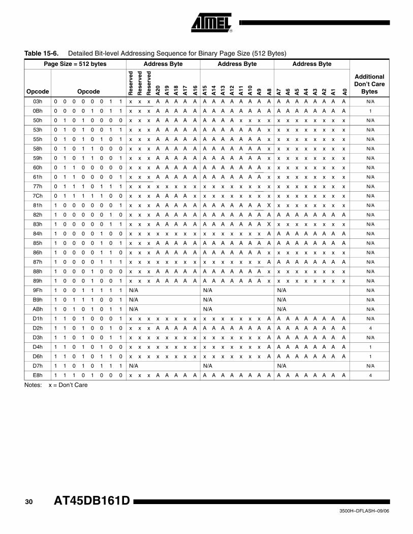
Table 15-6. Detailed Bit-level Addressing Sequence for Binary Page Size (512 Bytes)
Page Size = 512 bytes Address Byte Address Byte Address Byte
Additional Don’t Care
BytesOpcode Opcode Res
erve
d
Res
erve
d
Res
erve
d
A20
A19
A18
A17
A16
A15
A14
A13
A12
A11
A10
A9
A8
A7
A6
A5
A4
A3
A2
A1
A0
03h 0 0 0 0 0 0 1 1 x x x A A A A A A A A A A A A A A A A A A A A A N/A
0Bh 0 0 0 0 1 0 1 1 x x x A A A A A A A A A A A A A A A A A A A A A 1
50h 0 1 0 1 0 0 0 0 x x x A A A A A A A A A x x x x x x x x x x x x N/A
53h 0 1 0 1 0 0 1 1 x x x A A A A A A A A A A A A x x x x x x x x x N/A
55h 0 1 0 1 0 1 0 1 x x x A A A A A A A A A A A A x x x x x x x x x N/A
58h 0 1 0 1 1 0 0 0 x x x A A A A A A A A A A A A x x x x x x x x x N/A
59h 0 1 0 1 1 0 0 1 x x x A A A A A A A A A A A A x x x x x x x x x N/A
60h 0 1 1 0 0 0 0 0 x x x A A A A A A A A A A A A x x x x x x x x x N/A
61h 0 1 1 0 0 0 0 1 x x x A A A A A A A A A A A A x x x x x x x x x N/A
77h 0 1 1 1 0 1 1 1 x x x x x x x x x x x x x x x x x x x x x x x x N/A
7Ch 0 1 1 1 1 1 0 0 x x x A A A A x x x x x x x x x x x x x x x x x N/A
81h 1 0 0 0 0 0 0 1 x x x A A A A A A A A A A A A X x x x x x x x x N/A
82h 1 0 0 0 0 0 1 0 x x x A A A A A A A A A A A A A A A A A A A A A N/A
83h 1 0 0 0 0 0 1 1 x x x A A A A A A A A A A A A X x x x x x x x x N/A
84h 1 0 0 0 0 1 0 0 x x x x x x x x x x x x x x x A A A A A A A A A N/A
85h 1 0 0 0 0 1 0 1 x x x A A A A A A A A A A A A A A A A A A A A A N/A
86h 1 0 0 0 0 1 1 0 x x x A A A A A A A A A A A A x x x x x x x x x N/A
87h 1 0 0 0 0 1 1 1 x x x x x x x x x x x x x x x A A A A A A A A A N/A
88h 1 0 0 0 1 0 0 0 x x x A A A A A A A A A A A A x x x x x x x x x N/A
89h 1 0 0 0 1 0 0 1 x x x A A A A A A A A A A A A x x x x x x x x x N/A
9Fh 1 0 0 1 1 1 1 1 N/A N/A N/A N/A
B9h 1 0 1 1 1 0 0 1 N/A N/A N/A N/A
ABh 1 0 1 0 1 0 1 1 N/A N/A N/A N/A
D1h 1 1 0 1 0 0 0 1 x x x x x x x x x x x x x x x A A A A A A A A A N/A
D2h 1 1 0 1 0 0 1 0 x x x A A A A A A A A A A A A A A A A A A A A A 4
D3h 1 1 0 1 0 0 1 1 x x x x x x x x x x x x x x x A A A A A A A A A N/A
D4h 1 1 0 1 0 1 0 0 x x x x x x x x x x x x x x x A A A A A A A A A 1
D6h 1 1 0 1 0 1 1 0 x x x x x x x x x x x x x x x A A A A A A A A A 1
D7h 1 1 0 1 0 1 1 1 N/A N/A N/A N/A
E8h 1 1 1 0 1 0 0 0 x x x A A A A A A A A A A A A A A A A A A A A A 4
303500H–DFLASH–09/06
AT45DB161D
AT45DB161D
Notes: P = Page Address Bit B = Byte/Buffer Address Bit x = Don’t Care
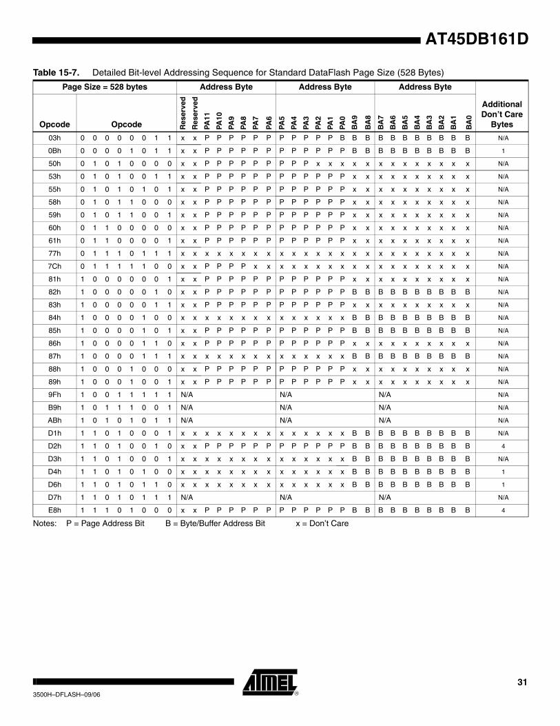
Table 15-7. Detailed Bit-level Addressing Sequence for Standard DataFlash Page Size (528 Bytes)
Page Size = 528 bytes Address Byte Address Byte Address Byte
Additional Don’t Care
BytesOpcode Opcode Res
erve
d
Res
erve
d
PA11
PA10
PA9
PA8
PA7
PA6
PA5
PA4
PA3
PA2
PA1
PA0
BA
9
BA
8
BA
7
BA
6
BA
5
BA
4
BA
3
BA
2
BA
1
BA
0
03h 0 0 0 0 0 0 1 1 x x P P P P P P P P P P P B B B B B B B B B B B N/A
0Bh 0 0 0 0 1 0 1 1 x x P P P P P P P P P P P P B B B B B B B B B B 1
50h 0 1 0 1 0 0 0 0 x x P P P P P P P P P x x x x x x x x x x x x x N/A
53h 0 1 0 1 0 0 1 1 x x P P P P P P P P P P P P x x x x x x x x x x N/A
55h 0 1 0 1 0 1 0 1 x x P P P P P P P P P P P P x x x x x x x x x x N/A
58h 0 1 0 1 1 0 0 0 x x P P P P P P P P P P P P x x x x x x x x x x N/A
59h 0 1 0 1 1 0 0 1 x x P P P P P P P P P P P P x x x x x x x x x x N/A
60h 0 1 1 0 0 0 0 0 x x P P P P P P P P P P P P x x x x x x x x x x N/A
61h 0 1 1 0 0 0 0 1 x x P P P P P P P P P P P P x x x x x x x x x x N/A
77h 0 1 1 1 0 1 1 1 x x x x x x x x x x x x x x x x x x x x x x x x N/A
7Ch 0 1 1 1 1 1 0 0 x x P P P P x x x x x x x x x x x x x x x x x x N/A
81h 1 0 0 0 0 0 0 1 x x P P P P P P P P P P P P x x x x x x x x x x N/A
82h 1 0 0 0 0 0 1 0 x x P P P P P P P P P P P P B B B B B B B B B B N/A
83h 1 0 0 0 0 0 1 1 x x P P P P P P P P P P P P x x x x x x x x x x N/A
84h 1 0 0 0 0 1 0 0 x x x x x x x x x x x x x x B B B B B B B B B B N/A
85h 1 0 0 0 0 1 0 1 x x P P P P P P P P P P P P B B B B B B B B B B N/A
86h 1 0 0 0 0 1 1 0 x x P P P P P P P P P P P P x x x x x x x x x x N/A
87h 1 0 0 0 0 1 1 1 x x x x x x x x x x x x x x B B B B B B B B B B N/A
88h 1 0 0 0 1 0 0 0 x x P P P P P P P P P P P P x x x x x x x x x x N/A
89h 1 0 0 0 1 0 0 1 x x P P P P P P P P P P P P x x x x x x x x x x N/A
9Fh 1 0 0 1 1 1 1 1 N/A N/A N/A N/A
B9h 1 0 1 1 1 0 0 1 N/A N/A N/A N/A
ABh 1 0 1 0 1 0 1 1 N/A N/A N/A N/A
D1h 1 1 0 1 0 0 0 1 x x x x x x x x x x x x x x B B B B B B B B B B N/A
D2h 1 1 0 1 0 0 1 0 x x P P P P P P P P P P P P B B B B B B B B B B 4
D3h 1 1 0 1 0 0 0 1 x x x x x x x x x x x x x x B B B B B B B B B B N/A
D4h 1 1 0 1 0 1 0 0 x x x x x x x x x x x x x x B B B B B B B B B B 1
D6h 1 1 0 1 0 1 1 0 x x x x x x x x x x x x x x B B B B B B B B B B 1
D7h 1 1 0 1 0 1 1 1 N/A N/A N/A N/A
E8h 1 1 1 0 1 0 0 0 x x P P P P P P P P P P P P B B B B B B B B B B 4
313500H–DFLASH–09/06
16. Power-on/Reset StateWhen power is first applied to the device, or when recovering from a reset condition, the devicewill default to Mode 3. In addition, the output pin (SO) will be in a high impedance state, and ahigh-to-low transition on the CS pin will be required to start a valid instruction. The mode (Mode3 or Mode 0) will be automatically selected on every falling edge of CS by sampling the inactiveclock state.
16.1 Initial Power-up/Reset Timing RestrictionsAt power up, the device must not be selected until the supply voltage reaches the VCC (min.) andfurther delay of tVCSL. During power-up, the internal Power-on Reset circuitry keeps the device inreset mode until the VCC rises above the Power-on Reset threshold value (VPOR). At this time, alloperations are disabled and the device does not respond to any commands. After power up isapplied and the VCC is at the minimum operating voltage VCC (min.), the tVCSL delay is requiredbefore the device can be selected in order to perform a read operation.
Similarly, the tPUW delay is required after the VCC rises above the Power-on Reset thresholdvalue (VPOR) before the device can perform a write (Program or Erase) operation. After initialpower-up, the device will default in Standby mode.
17. System ConsiderationsThe RapidS serial interface is controlled by the clock SCK, serial input SI and chip select CSpins. These signals must rise and fall monotonically and be free from noise. Excessive noise orringing on these pins can be misinterpreted as multiple edges and cause improper operation ofthe device. The PC board traces must be kept to a minimum distance or appropriately termi-nated to ensure proper operation. If necessary, decoupling capacitors can be added on thesepins to provide filtering against noise glitches.
As system complexity continues to increase, voltage regulation is becoming more important. Akey element of any voltage regulation scheme is its current sourcing capability. Like all Flashmemories, the peak current for DataFlash occur during the programming and erase operation.The regulator needs to supply this peak current requirement. An under specified regulator cancause current starvation. Besides increasing system noise, current starvation during program-ming or erase can lead to improper operation and possible data corruption.
Symbol Parameter Min Typ Max Units
tVCSL VCC (min.) to Chip Select low 50 µs
tPUW Power-Up Device Delay before Write Allowed 20 ms
VPOR Power-ON Reset Voltage 1.5 2.5 V
323500H–DFLASH–09/06
AT45DB161D

AT45DB161D
18. Electrical Specifications
Notes: 1. ICC1 during a buffer read is 20 mA maximum @ 20 MHz.
2. All inputs are 5 volts tolerant.
Table 18-1. Absolute Maximum Ratings*
Temperature under Bias ................................ -55°C to +125°C *NOTICE: Stresses beyond those listed under “Absolute Maximum Ratings” may cause permanent dam-age to the device. This is a stress rating only and functional operation of the device at these or any other conditions beyond those indicated in the operational sections of this specification is not implied. Exposure to absolute maximum rating conditions for extended periods may affect device reliability.
Storage Temperature ..................................... -65°C to +150°C
All Input Voltages (including NC Pins)with Respect to Ground ...................................-0.6V to +6.25V
All Output Voltageswith Respect to Ground .............................-0.6V to VCC + 0.6V
Table 18-2. DC and AC Operating Range
AT45DB161D (2.5V Version) AT45DB161D
Operating Temperature (Case) Ind. -40°C to 85°C -40°C to 85°C
VCC Power Supply 2.5V to 3.6V 2.7V to 3.6V
Table 18-3. DC Characteristics
Symbol Parameter Condition Min Typ Max Units
IDP Deep Power-down Current CS, RESET, WP = VIH, all inputs at CMOS levels
9 15 µA
ISB Standby CurrentCS, RESET, WP = VIH, all inputs at CMOS levels
25 50 µA
ICC1(1) Active Current, Read Operation
f = 20 MHz; IOUT = 0 mA; VCC = 3.6V
7 10 mA
f = 33 MHz; IOUT = 0 mA; VCC = 3.6V
8 12 mA
f = 50 MHz; IOUT = 0 mA; VCC = 3.6V
10 14 mA
f = 66 MHz; IOUT = 0 mA; VCC = 3.6V
11 15 mA
ICC2Active Current, Program/Erase Operation
VCC = 3.6V 12 17 mA
ILI Input Load Current VIN = CMOS levels 1 µA
ILO Output Leakage Current VI/O = CMOS levels 1 µA
VIL Input Low Voltage VCC x 0.3 V
VIH Input High Voltage VCC x 0.7 V
VOL Output Low Voltage IOL = 1.6 mA; VCC = 2.7V 0.4 V
VOH Output High Voltage IOH = -100 µA VCC - 0.2V V
333500H–DFLASH–09/06

Note: 1. Values are based on device characterization, not 100% tested in production.
Table 18-4. AC Characteristics – RapidS/Serial Interface
Symbol Parameter
AT45DB161D (2.5V Version) AT45DB161D
Min Typ Max Min Typ Max Units
fSCK SCK Frequency 50 66 MHz
fCAR1 SCK Frequency for Continuous Array Read 50 66 MHz
fCAR2SCK Frequency for Continuous Array Read(Low Frequency)
33 33 MHz
tWH SCK High Time 6.8 6.8 ns
tWL SCK Low Time 6.8 6.8 ns
tSCKR(1) SCK Rise Time, Peak-to-Peak (Slew Rate) 0.1 0.1 V/ns
tSCKF(1) SCK Fall Time, Peak-to-Peak (Slew Rate) 0.1 0.1 V/ns
tCS Minimum CS High Time 50 50 ns
tCSS CS Setup Time 5 5 ns
tCSH CS Hold Time 5 5 ns
tCSB CS High to RDY/BUSY Low 100 100 ns
tSU Data In Setup Time 2 2 ns
tH Data In Hold Time 3 3 ns
tHO Output Hold Time 0 0 ns
tDIS Output Disable Time 8 6 ns
tV Output Valid 8 6 ns
tWPE WP Low to Protection Enabled 1 1 µs
tWPD WP High to Protection Disabled 1 1 µs
tEDPD CS High to Deep Power-down Mode 3 3 µs
tRDPD CS High to Standby Mode 30 30 µs
tXFR Page to Buffer Transfer Time 400 400 µs
tcomp Page to Buffer Compare Time 400 400 µs
tEPPage Erase and Programming Time (512/528 bytes)
17 40 17 40 ms
tP Page Programming Time (512/528 bytes) 3 6 3 6 ms
tPE Page Erase Time (512/528 bytes) 15 35 15 35 ms
tBE Block Erase Time (4096/4224 bytes) 45 100 45 100 ms
tSE Sector Erase Time (131,072/135,168 bytes) 1.6 5 1.6 5 s
tCE Chip Erase Time TBD TBD TBD TBD s
tRST RESET Pulse Width 10 10 µs
tREC RESET Recovery Time 1 1 µs
343500H–DFLASH–09/06
AT45DB161D
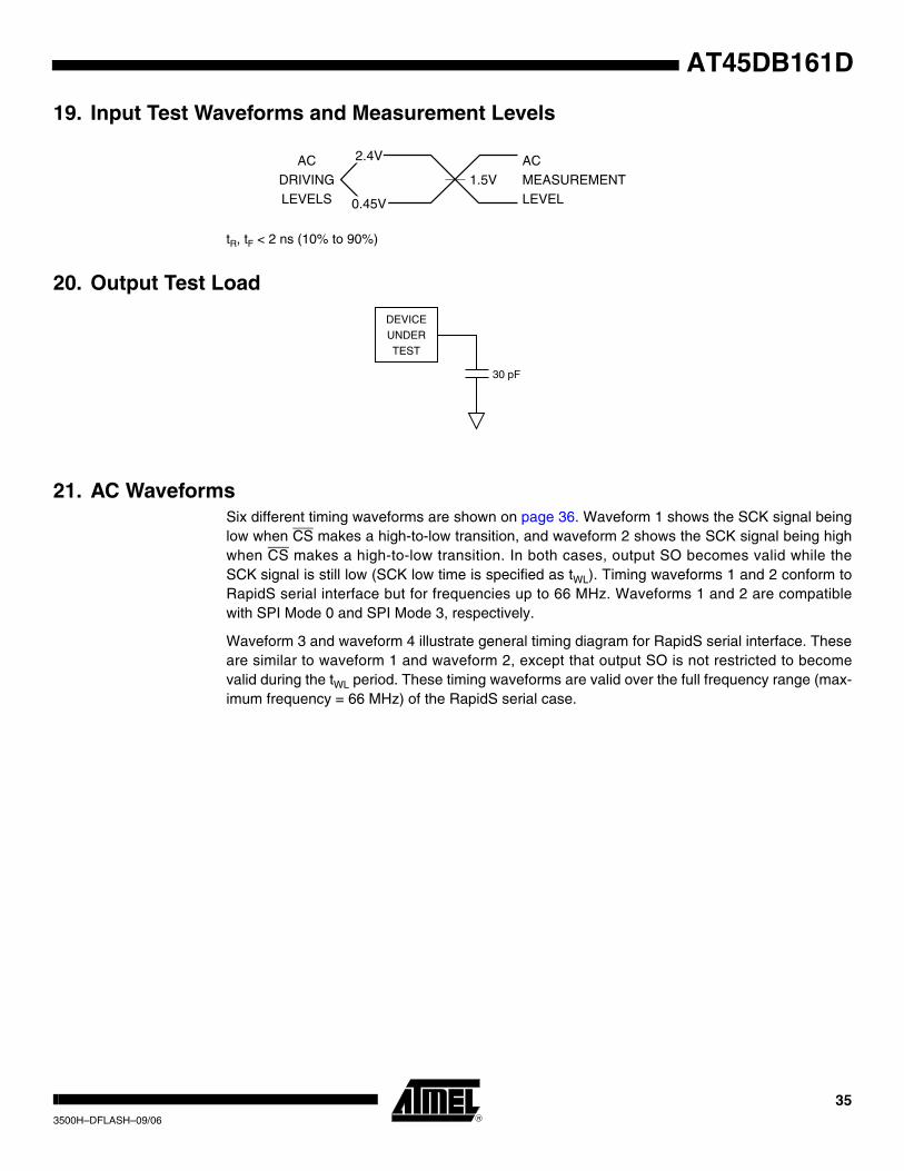
AT45DB161D
19. Input Test Waveforms and Measurement Levels
tR, tF < 2 ns (10% to 90%)
20. Output Test Load
21. AC WaveformsSix different timing waveforms are shown on page 36. Waveform 1 shows the SCK signal beinglow when CS makes a high-to-low transition, and waveform 2 shows the SCK signal being highwhen CS makes a high-to-low transition. In both cases, output SO becomes valid while theSCK signal is still low (SCK low time is specified as tWL). Timing waveforms 1 and 2 conform toRapidS serial interface but for frequencies up to 66 MHz. Waveforms 1 and 2 are compatiblewith SPI Mode 0 and SPI Mode 3, respectively.
Waveform 3 and waveform 4 illustrate general timing diagram for RapidS serial interface. Theseare similar to waveform 1 and waveform 2, except that output SO is not restricted to becomevalid during the tWL period. These timing waveforms are valid over the full frequency range (max-imum frequency = 66 MHz) of the RapidS serial case.
ACDRIVINGLEVELS
ACMEASUREMENTLEVEL0.45V
1.5V
2.4V
DEVICEUNDERTEST
30 pF
353500H–DFLASH–09/06

21.1 Waveform 1 – SPI Mode 0 Compatible (for frequencies up to 66 MHz)
21.2 Waveform 2 – SPI Mode 3 Compatible (for frequencies up to 66 MHz)
21.3 Waveform 3 – RapidS Mode 0 (FMAX = 66 MHz)
21.4 Waveform 4 – RapidS Mode 3 (FMAX = 66 MHz)
CS
SCK
SI
SO
tCSS
VALID IN
tHtSU
tWH tWL tCSH
tCS
tVHIGH IMPEDANCE
VALID OUT
tHO tDIS
HIGH IMPEDANCE
CS
SCK
SO
tCSS
VALID IN
tHtSU
tWL tWH tCSH
tCS
tVHIGH Z
VALID OUT
tHO tDIS
HIGH IMPEDANCE
SI
CS
SCK
SI
SO
tCSS
VALID IN
tHtSU
tWH tWL tCSH
tCS
tVHIGH IMPEDANCE
VALID OUT
tHO tDIS
HIGH IMPEDANCE
CS
SCK
SO
tCSS
VALID IN
tHtSU
tWL tWH tCSH
tCS
tVHIGH Z
VALID OUT
tHO tDIS
HIGH IMPEDANCE
SI
363500H–DFLASH–09/06
AT45DB161D

AT45DB161D
21.5 Utilizing the RapidS™ FunctionTo take advantage of the RapidS function's ability to operate at higher clock frequencies, a fullclock cycle must be used to transmit data back and forth across the serial bus. The DataFlash isdesigned to always clock its data out on the falling edge of the SCK signal and clock data in onthe rising edge of SCK.
For full clock cycle operation to be achieved, when the DataFlash is clocking data out on the fall-ing edge of SCK, the host controller should wait until the next falling edge of SCK to latch thedata in. Similarly, the host controller should clock its data out on the rising edge of SCK in orderto give the DataFlash a full clock cycle to latch the incoming data in on the next rising edge ofSCK.
Figure 21-1. RapidS Mode
SCK
MOSI
MISO
12 3 4 5 6 7
8 12 3 4 5 6 7
8
MOSI = Master Out, Slave InMISO = Master In, Slave OutThe Master is the host controller and the Slave is the DataFlash
The Master always clocks data out on the rising edge of SCK and always clocks data in on the falling edge of SCK.The Slave always clocks data out on the falling edge of SCK and always clocks data in on the rising edge of SCK.
A. Master clocks out first bit of BYTE-MOSI on the rising edge of SCK.B. Slave clocks in first bit of BYTE-MOSI on the next rising edge of SCK.C. Master clocks out second bit of BYTE-MOSI on the same rising edge of SCK.D. Last bit of BYTE-MOSI is clocked out from the Master.E. Last bit of BYTE-MOSI is clocked into the slave.F. Slave clocks out first bit of BYTE-SO.G. Master clocks in first bit of BYTE-SO.H. Slave clocks out second bit of BYTE-SO.I. Master clocks in last bit of BYTE-SO.
AB
C DE
FG
1
HBYTE-MOSI
MSB LSB
BYTE-SO
MSB LSB
Slave CS
I
373500H–DFLASH–09/06

21.6 Reset Timing
Note: The CS signal should be in the high state before the RESET signal is deasserted.
21.7 Command Sequence for Read/Write Operations for Page Size 512 Bytes (Except Status Register Read, Manufacturer and Device ID Read)
21.8 Command Sequence for Read/Write Operations for Page Size 528 Bytes (Except Status Register Read, Manufacturer and Device ID Read)
CS
SCK
RESET
SO (OUTPUT)HIGH IMPEDANCE HIGH IMPEDANCE
SI (INPUT)
tRST
tREC tCSS
SI (INPUT) CMD 8 bits 8 bits 8 bits
Page Address(A20 - A9)
X X X X X X X X X X X X X X X X LSBX X X X X X X X
Byte/Buffer Address(A8 - A0/BFA8 - BFA0)
MSB
Don’t Care Bits
Page Address(PA11 - PA0)
Byte/Buffer Address(BA9 - BA0/BFA9 - BFA0)
SI (INPUT) CMD 8 bits 8 bits 8 bits
X X X X X X X X X X X X LSBX X X X X X X XMSB
2 Don’t Care Bits
X X X X
383500H–DFLASH–09/06
AT45DB161D

AT45DB161D
22. Write OperationsThe following block diagram and waveforms illustrate the various write sequences available.
22.1 Buffer Write
22.2 Buffer to Main Memory Page Program (Data from Buffer Programmed into Flash Page)
FLASH MEMORY ARRAY
PAGE (512/528 BYTES)
BUFFER 2 (512/528 BYTES)BUFFER 1 (512/528 BYTES)
I/O INTERFACE
SI
BUFFER 1 TOMAIN MEMORY
PAGE PROGRAM
BUFFER 2 TOMAIN MEMORYPAGE PROGRAM
BUFFER 1WRITE
BUFFER 2WRITE
SI (INPUT) CMD
Completes writing into selected buffer
CS
X X···X, BFA9-8 BFA7-0 n n+1 Last Byte
BINARY PAGE SIZE15 DON'T CARE + BFA8-BFA0
SI (INPUT) CMD PA11-6 PA5-0, XX
CS
Starts self-timed erase/program operation
XXXX XX
Each transition represents 8 bits
n = 1st byte readn+1 = 2nd byte read
BINARY PAGE SIZEA20-A9 + 9 DON'T CARE BITS
393500H–DFLASH–09/06

23. Read OperationsThe following block diagram and waveforms illustrate the various read sequences available.
23.1 Main Memory Page Read
23.2 Main Memory Page to Buffer Transfer (Data from Flash Page Read into Buffer)
FLASH MEMORY ARRAY
PAGE (512/528 BYTES)
BUFFER 2 (512/528 BYTES)BUFFER 1 (512/528 BYTES)
I/O INTERFACE
MAIN MEMORYPAGE TO
BUFFER 1
MAIN MEMORYPAGE TOBUFFER 2
MAIN MEMORYPAGE READ
BUFFER 1READ
BUFFER 2READ
SO
SI (INPUT) CMD PA11-6 , PA5-0, BA9-8 X
CS
n n+1SO (OUTPUT)
BA7-0
4 Dummy Bytes
X
ADDRESS FOR BINARY PAGE SIZEA20-A16 A15-A8 A7-A0
Starts reading page data into buffer
SI (INPUT) CMD PA11-6 PA5-0, XX
CS
SO (OUTPUT)
XXXX XXXX
BINARY PAGE SIZEA20-A9 + 9 DON'T CARE BITS
403500H–DFLASH–09/06
AT45DB161D
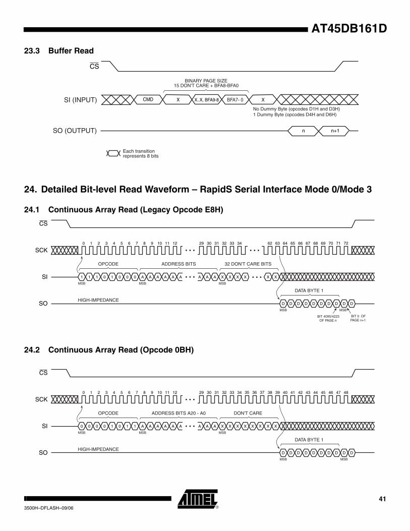
AT45DB161D
23.3 Buffer Read
24. Detailed Bit-level Read Waveform – RapidS Serial Interface Mode 0/Mode 3
24.1 Continuous Array Read (Legacy Opcode E8H)
24.2 Continuous Array Read (Opcode 0BH)
CMD
CS
n n+1
XX X..X, BFA9-8 BFA7- 0
BINARY PAGE SIZE15 DON'T CARE + BFA8-BFA0
Each transitionrepresents 8 bits
SI (INPUT)
SO (OUTPUT)
No Dummy Byte (opcodes D1H and D3H)1 Dummy Byte (opcodes D4H and D6H)
SCK
CS
SI
SO
MSB MSB
2 310
1 1 1 0 1 0 0 0
6 754 10 1198 12 63 66 6765646233 3431 3229 30 68 71 727069
OPCODE
A A A A A A AA A
MSB
X X X X X X
MSB MSB
D D D D D D D DDD
ADDRESS BITS 32 DON'T CARE BITS
DATA BYTE 1
HIGH-IMPEDANCE
BIT 4095/4223OF PAGE n
BIT 0 OFPAGE n+1
SCK
CS
SI
SO
MSB MSB
2 310
0 0 0 0 1 0 1 1
6 754 10 1198 12 39 42 4341403833 3431 3229 30 44 47 484645
OPCODE
A A A A A A AA A
MSB
X X X X X X
MSB MSB
D D D D D D D DDD
ADDRESS BITS A20 - A0 DON'T CARE
DATA BYTE 1
HIGH-IMPEDANCE
36 3735
X X
413500H–DFLASH–09/06

24.3 Continuous Array Read (Low Frequency: Opcode 03H)
24.4 Main Memory Page Read (Opcode: D2H)
24.5 Buffer Read (Opcode D4H or D6H)
SCK
CS
SI
SO
MSB MSB
2 310
0 0 0 0 0 0 1 1
6 754 10 1198 12 37 3833 36353431 3229 30 39 40
OPCODE
A A A A A A AA A
MSB MSB
D D D D D D D DDD
ADDRESS BITS A20-A0
DATA BYTE 1
HIGH-IMPEDANCE
SCK
CS
SI
SO
MSB MSB
2 310
1 1 0 1 0 0 1 0
6 754 10 1198 12 63 66 6765646233 3431 3229 30 68 71 727069
OPCODE
A A A A A A AA A
MSB
X X X X X X
MSB MSB
D D D D D D D DDD
ADDRESS BITS 32 DON'T CARE BITS
DATA BYTE 1
HIGH-IMPEDANCE
SCK
CS
SI
SO
MSB MSB
2 310
1 1 0 1 0 1 0 0
6 754 10 1198 12 39 42 43414037 3833 36353431 3229 30 44 47 484645
OPCODE
X X X X A A AX X
MSB
X X X X X X X X
MSB MSB
D D D D D D D DDD
ADDRESS BITSBINARY PAGE SIZE = 15 DON'T CARE + BFA8-BFA0STANDARD DATAFLASH PAGE SIZE = 14 DON'T CARE + BFA9-BFA0
DON'T CARE
DATA BYTE 1
HIGH-IMPEDANCE
423500H–DFLASH–09/06
AT45DB161D

AT45DB161D
24.6 Buffer Read (Low Frequency: Opcode D1H or D3H)
24.7 Read Sector Protection Register (Opcode 32H)
24.8 Read Sector Lockdown Register (Opcode 35H)
SCK
CS
SI
SO
MSB MSB
2 310
1 1 0 1 0 0 0 1
6 754 10 1198 12 37 3833 36353431 3229 30 39 40
OPCODE
X X X X A A AX X
MSB MSB
D D D D D D D DDD
DATA BYTE 1
HIGH-IMPEDANCE
ADDRESS BITSBINARY PAGE SIZE = 15 DON'T CARE + BFA8-BFA0STANDARD DATAFLASH PAGE SIZE = 14 DON'T CARE + BFA9-BFA0
SCK
CS
SI
SO
MSB MSB
2 310
0 0 1 1 0 0 1 0
6 754 10 1198 12 37 3833 36353431 3229 30 39 40
OPCODE
X X X X X X XX X
MSB MSB
D D D D D D DDD
DON'T CARE
DATA BYTE 1
HIGH-IMPEDANCE
SCK
CS
SI
SO
MSB MSB
2 310
0 0 1 1 0 1 0 1
6 754 10 1198 12 37 3833 36353431 3229 30 39 40
OPCODE
X X X X X X XX X
MSB MSB
D D D D D D DDD
DON'T CARE
DATA BYTE 1
HIGH-IMPEDANCE
433500H–DFLASH–09/06

24.9 Read Security Register (Opcode 77H)
24.10 Status Register Read (Opcode D7H)
24.11 Manufacturer and Device Read (Opcode 9FH)
SCK
CS
SI
SO
MSB MSB
2 310
0 1 1 1 0 1 1 1
6 754 10 1198 12 37 3833 36353431 3229 30 39 40
OPCODE
X X X X X X XX X
MSB MSB
D D D D D D DDD
DON'T CARE
DATA BYTE 1
HIGH-IMPEDANCE
SCK
CS
SI
SO
MSB
2 310
1 1 0 1 0 1 1 1
6 754 10 1198 12 21 2217 20191815 1613 14 23 24
OPCODE
MSB MSB
D D D D D D D DDD
MSB
D D D D D DDD
STATUS REGISTER DATA STATUS REGISTER DATA
HIGH-IMPEDANCE
SCK
CS
SI
SO
60
9FH
87 38
OPCODE
1FH DEVICE ID BYTE 1 DEVICE ID BYTE 2 00HHIGH-IMPEDANCE
14 1615 22 2423 30 3231
Note: Each transition shown for SI and SO represents one byte (8 bits)
443500H–DFLASH–09/06
AT45DB161D

AT45DB161D
25. Auto Page Rewrite Flowchart
Figure 25-1. Algorithm for Programming or Reprogramming of the Entire Array Sequentially
Notes: 1. This type of algorithm is used for applications in which the entire array is programmed sequentially, filling the array page-by-page.
2. A page can be written using either a Main Memory Page Program operation or a Buffer Write operation followed by a Buffer to Main Memory Page Program operation.
3. The algorithm above shows the programming of a single page. The algorithm will be repeated sequentially for each page within the entire array.
START
MAIN MEMORY PAGE PROGRAMTHROUGH BUFFER
(82H, 85H)
END
provide addressand data
BUFFER WRITE(84H, 87H)
BUFFER TO MAINMEMORY PAGE PROGRAM
(83H, 86H)
453500H–DFLASH–09/06

Figure 25-2. Algorithm for Randomly Modifying Data
Notes: 1. To preserve data integrity, each page of a DataFlash sector must be updated/rewritten at least once within every 10,000 cumulative page erase and program operations.
2. A Page Address Pointer must be maintained to indicate which page is to be rewritten. The Auto Page Rewrite command must use the address specified by the Page Address Pointer.
3. Other algorithms can be used to rewrite portions of the Flash array. Low-power applications may choose to wait until 10,000 cumulative page erase and program operations have accumulated before rewriting all pages of the sector. See application note AN-4 (“Using Atmel’s Serial DataFlash”) for more details.
START
MAIN MEMORY PAGETO BUFFER TRANSFER
(53H, 55H)
INCREMENT PAGEADDRESS POINTER
(2)
AUTO PAGE REWRITE(2)
(58H, 59H)
END
provide address ofpage to modify
If planning to modify multiplebytes currently stored withina page of the Flash array
MAIN MEMORY PAGE PROGRAMTHROUGH BUFFER
(82H, 85H)
BUFFER WRITE(84H, 87H)
BUFFER TO MAINMEMORY PAGE PROGRAM
(83H, 86H)
463500H–DFLASH–09/06
AT45DB161D

AT45DB161D
26. Ordering Information
26.1 Green Package Options (Pb/Halide-free/RoHS Compliant)
fSCK (MHz)
ICC (mA)
Ordering Code Package Operation RangeActive Standby
66 15 0.05
AT45DB161D-SU 8S2Industrial
(-40°C to 85°C)
2.7V to 3.6V
AT45DB161D-MU 8M1-A
AT45DB161D-TU 28T
50 15 0.05
AT45DB161D-SU-2.5 8S2Industrial
(-40°C to 85°C)
2.5V to 3.6V
AT45DB161D-MU-2.5 8M1-A
AT45DB161D-TU-2.5 28T
Package Type
8S2 8-lead, 0.209” Wide, Plastic Gull Wing Small Outline Package (EIAJ SOIC)
8M1-A 8-contact, 5 mm x 6 mm Very Thin Micro Lead-frame Package (MLF)
28T 28-lead, 8 mm x 13.4 mm, Plastic Thin Small Outline Package, Type I (TSOP)
473500H–DFLASH–09/06

27. Packaging Information
27.1 8S2 – EIAJ SOIC
2325 Orchard ParkwaySan Jose, CA 95131
TITLE DRAWING NO.
R
REV. 8S2, 8-lead, 0.209" Body, Plastic Small Outline Package (EIAJ)
4/7/06
8S2 D
COMMON DIMENSIONS(Unit of Measure = mm)
SYMBOL MIN NOM MAX NOTE
Notes: 1. This drawing is for general information only; refer to EIAJ Drawing EDR-7320 for additional information. 2. Mismatch of the upper and lower dies and resin burrs are not included. 3. It is recommended that upper and lower cavities be equal. If they are different, the larger dimension shall be regarded. 4. Determines the true geometric position. 5. Values b,C apply to plated terminal. The standard thickness of the plating layer shall measure between 0.007 to .021 mm.
A 1.70 2.16
A1 0.05 0.25
b 0.35 0.48 5
C 0.15 0.35 5
D 5.13 5.35
E1 5.18 5.40 2, 3
E 7.70 8.26
L 0.51 0.85
θ 0° 8°
e 1.27 BSC 4
θθ
11
NN
EE
TOP VIEWTOP VIEW
CC
E1E1
END VIEWEND VIEW
AA
bb
LL
A1A1
ee
DD
SIDE VIEWSIDE VIEW
483500H–DFLASH–09/06
AT45DB161D

AT45DB161D
27.2 8M1-A – MLF
2325 Orchard Parkway San Jose, CA 95131
TITLE DRAWING NO.
R
REV. 8M1-A, 8-pad, 6 x 5 x 1.00 mm Body, Very Thin Dual Flat PackageNo Lead (MLF) C8M1-A
9/8/06
COMMON DIMENSIONS(Unit of Measure = mm)
SYMBOL MIN NOM MAX NOTE
A – 0.85 1.00
A1 – – 0.05
A2 0.65 TYP
A3 0.20 TYP
b 0.35 0.40 0.48
D 5.90 6.00 6.10
D1 5.70 5.75 5.80
D2 3.20 3.40 3.60
E 4.90 5.00 5.10
E1 4.70 4.75 4.80
E2 3.80 4.00 4.20
e 1.27
L 0.50 0.60 0.75
– – 12o
K 0.25 – –
Pin 1 ID
TOP VIEW
Pin #1 Notch(0.20 R)
BOTTOM VIEW
D2
E2
L
b
D1
D
E1E
e
A3A2
A1 A
0.08 C
0
SIDE VIEW
0
K
0.45
493500H–DFLASH–09/06

27.3 28T – TSOP, Type 1
2325 Orchard Parkway San Jose, CA 95131
TITLE DRAWING NO.
R
REV. 28T, 28-lead (8 x 13.4 mm) Plastic Thin Small Outline Package, Type I (TSOP)
C28T
12/06/02
PIN 10º ~ 5º
D1 D
Pin 1 Identifier Area
be
E A
A1
A2
c
L
GAGE PLANESEATING PLANE
L1
COMMON DIMENSIONS(Unit of Measure = mm)
SYMBOL MIN NOM MAX NOTE
Notes: 1. This package conforms to JEDEC reference MO-183. 2. Dimensions D1 and E do not include mold protrusion. Allowable
protrusion on E is 0.15 mm per side and on D1 is 0.25 mm per side.3. Lead coplanarity is 0.10 mm maximum.
A – – 1.20
A1 0.05 – 0.15
A2 0.90 1.00 1.05
D 13.20 13.40 13.60
D1 11.70 11.80 11.90 Note 2
E 7.90 8.00 8.10 Note 2
L 0.50 0.60 0.70
L1 0.25 BASIC
b 0.17 0.22 0.27
c 0.10 – 0.21
e 0.55 BASIC
503500H–DFLASH–09/06
AT45DB161D

AT45DB161D
28. Revision History
Revision Level – Release Date History
A – September 2005 Initial Release
B – November 2005
Added 2.5V - 3.6V operating range.
Changed tVCSL from 30 µs to 50 µs min.
Changed tPUW from 10 ms to 20 ms max.Changed tDIS from 8 ns to 6 ns max (2.7-volt device).
Changed tV from 8 ns to 6 ns max (2.7-volt device).
C – January 2006
Added text, in “Programming the Configuration Register”, to indicate that power cycling is required to switch to “power of 2” page size after the opcode enable has been executed.
Added “Legacy Commands” table.
D – February 2006 Changed part 2 of the device ID to 00H.
E – May 2006Added Legacy Status Register Read opcode 57H. This opcode is supported on devices with date code 0636 and later.
F – July 2006 Corrected typographical errors.
G – August 2006 Added errata regarding Chip Erase.
513500H–DFLASH–09/06

29. Errata
29.1 Chip Erase
29.1.1 IssueIn a certain percentage of units, the Chip Erase feature may not function correctly and mayadversely affect device operation. Therefore, it is recommended that the Chip Erase commands(opcodes C7H, 94H, 80H, and 9AH) not be used.
29.1.2 WorkaroundUse Block Erase (opcode 50H) as an alternative. The Block Erase function is not affected by theChip Erase issue.
29.1.3 ResolutionThe Chip Erase feature may be fixed with a new revision of the device. Please contact Atmel forthe estimated availability of devices with the fix.
523500H–DFLASH–09/06
AT45DB161D
3500H–DFLASH–09/06
Disclaimer: The information in this document is provided in connection with Atmel products. No license, express or implied, by estoppel or otherwise, to anyintellectual property right is granted by this document or in connection with the sale of Atmel products. EXCEPT AS SET FORTH IN ATMEL’S TERMS AND CONDI-TIONS OF SALE LOCATED ON ATMEL’S WEB SITE, ATMEL ASSUMES NO LIABILITY WHATSOEVER AND DISCLAIMS ANY EXPRESS, IMPLIED OR STATUTORYWARRANTY RELATING TO ITS PRODUCTS INCLUDING, BUT NOT LIMITED TO, THE IMPLIED WARRANTY OF MERCHANTABILITY, FITNESS FOR A PARTICULARPURPOSE, OR NON-INFRINGEMENT. IN NO EVENT SHALL ATMEL BE LIABLE FOR ANY DIRECT, INDIRECT, CONSEQUENTIAL, PUNITIVE, SPECIAL OR INCIDEN-TAL DAMAGES (INCLUDING, WITHOUT LIMITATION, DAMAGES FOR LOSS OF PROFITS, BUSINESS INTERRUPTION, OR LOSS OF INFORMATION) ARISING OUTOF THE USE OR INABILITY TO USE THIS DOCUMENT, EVEN IF ATMEL HAS BEEN ADVISED OF THE POSSIBILITY OF SUCH DAMAGES. Atmel makes norepresentations or warranties with respect to the accuracy or completeness of the contents of this document and reserves the right to make changes to specificationsand product descriptions at any time without notice. Atmel does not make any commitment to update the information contained herein. Unless specifically providedotherwise, Atmel products are not suitable for, and shall not be used in, automotive applications. Atmel’s products are not intended, authorized, or warranted for useas components in applications intended to support or sustain life.
Atmel Corporation Atmel Operations
2325 Orchard ParkwaySan Jose, CA 95131, USATel: 1(408) 441-0311Fax: 1(408) 487-2600
Regional Headquarters
EuropeAtmel SarlRoute des Arsenaux 41Case Postale 80CH-1705 FribourgSwitzerlandTel: (41) 26-426-5555Fax: (41) 26-426-5500
AsiaRoom 1219Chinachem Golden Plaza77 Mody Road TsimshatsuiEast KowloonHong KongTel: (852) 2721-9778Fax: (852) 2722-1369
Japan9F, Tonetsu Shinkawa Bldg.1-24-8 ShinkawaChuo-ku, Tokyo 104-0033JapanTel: (81) 3-3523-3551Fax: (81) 3-3523-7581
Memory2325 Orchard ParkwaySan Jose, CA 95131, USATel: 1(408) 441-0311Fax: 1(408) 436-4314
Microcontrollers2325 Orchard ParkwaySan Jose, CA 95131, USATel: 1(408) 441-0311Fax: 1(408) 436-4314
La ChantrerieBP 7060244306 Nantes Cedex 3, FranceTel: (33) 2-40-18-18-18Fax: (33) 2-40-18-19-60
ASIC/ASSP/Smart CardsZone Industrielle13106 Rousset Cedex, FranceTel: (33) 4-42-53-60-00Fax: (33) 4-42-53-60-01
1150 East Cheyenne Mtn. Blvd.Colorado Springs, CO 80906, USATel: 1(719) 576-3300Fax: 1(719) 540-1759
Scottish Enterprise Technology ParkMaxwell BuildingEast Kilbride G75 0QR, Scotland Tel: (44) 1355-803-000Fax: (44) 1355-242-743
RF/AutomotiveTheresienstrasse 2Postfach 353574025 Heilbronn, GermanyTel: (49) 71-31-67-0Fax: (49) 71-31-67-2340
1150 East Cheyenne Mtn. Blvd.Colorado Springs, CO 80906, USATel: 1(719) 576-3300Fax: 1(719) 540-1759
Biometrics/Imaging/Hi-Rel MPU/High Speed Converters/RF Datacom
Avenue de RochepleineBP 12338521 Saint-Egreve Cedex, FranceTel: (33) 4-76-58-30-00Fax: (33) 4-76-58-34-80
Literature Requestswww.atmel.com/literature
© 2006 Atmel Corporation. All rights reserved. Atmel®, logo and combinations thereof, Everywhere You Are®, DataFlash®, and others areregistered trademarks; RapidS™ and others are trademarks of Atmel Corporation or its subsidiaries. Other terms and product names may betrademarks of others.