38 comparative area and parasitics analysis in finfet and
TRANSCRIPT

38
Comparative Area and Parasitics Analysis in FinFETand Heterojunction Vertical TFET Standard Cells
MOON SEOK KIM, WILLIAM CANE-WISSING, XUEQING LI, and JACK SAMPSON,The Pennsylvania State UniversitySUMAN DATTA, University of Notre DameSUMEET KUMAR GUPTA and VIJAYKRISHNAN NARAYANAN,The Pennsylvania State University
Vertical tunnel field-effect transistors (VTFETs) have been extensively explored to overcome the scaling lim-its and to improve on-current (ION) compared to standard lateral device structures for the future technologies.The benefits in terms of reduced footprint, high ION and feasibility of fabrication have been demonstratedin several works. Among various VTFETs, the asymmetric heterojunction vertical tunnel FETs (HVTFETs)have emerged as one of the promising alternatives to standard transistors for low-voltage applications. How-ever, while such device-level benefits without parasitics have been widely investigated, logic-gate designwith parasitics and layout implications are not clear. In this article, we investigate and compare the layoutsand parasitic capacitances and resistances of HVTFETs with FinFETs. Due to the vertical device structureof HVTFETs, a smaller footprint is observed compared to FinFETs in cells with small fan-in. However, forhigh fan-in cells, HVTFETs exhibit area overheads due to infeasibility of contact sharing in parallel andseries transistors. These area overheads also lead to approximately 48% higher parasitic capacitance andresistance compared to FinFETs when the number of parallel and series connections increases. Further, inorder to analyze the impact of parasitics, we modeled the analytical parasitics in SPICE. The models forboth HVTFETs and FinFETs with parasitics were used to simulate a 15-stage inverter-based ring oscillator(RO) in order to compare the delay and energy. Our simulation results clearly show that HVTFETs exhibitless delay at a VDD < 0.45 V and higher energy efficiency for VDDs in the range of 0.3V–0.7V, albeit at thecost of 8% performance degradation.
CCS Concepts: ! Hardware → Emerging technologies; Modeling and parameter extraction
Additional Key Words and Phrases: Standard cell, FinFET, tunnel FET, asymmetric vertical TFET, layout,area, parasitic capacitance, and parasitic resistance
This work was supported in part by the Center for Low Energy Systems Technology (LEAST), one of thesix SRC STARnet Centers, sponsored by MARCO and DARPA. The work is also supported in part throughinfrastructure provided by NSF Award 1205618.Authors’ addresses: M. S. Kim, 351 Information Sciences and Technology Building, The PennsylvaniaState University, University Park, PA 16802 USA; email: [email protected]; W. Cane-Wissing, 121Electrical Engineering East, The Pennsylvania State University, University Park, PA 16802 USA; email:[email protected]; X. Li, 351 Information Sciences and Technology Building, The Pennsylvania StateUniversity, University Park, PA 16802 USA; email: [email protected]; J. Sampson, 354E InformationSciences and Technology Building, The Pennsylvania State University, University Park, PA 16802 USA;email: [email protected]; S. Datta, 271 Fitzpatrick Hall, University of Notre Dame, IN 46556 USA;email: [email protected]; S. K. Gupta, 111K Electrical Engineering West, The Pennsylvania State University,University Park, PA 16802 USA; email: [email protected]; V. Narayanan, 354D Information Sciencesand Technology Building, The Pennsylvania State University, University Park, PA 16802 USA; email:[email protected] to make digital or hard copies of part or all of this work for personal or classroom use is grantedwithout fee provided that copies are not made or distributed for profit or commercial advantage and thatcopies show this notice on the first page or initial screen of a display along with the full citation. Copyrights forcomponents of this work owned by others than ACM must be honored. Abstracting with credit is permitted.To copy otherwise, to republish, to post on servers, to redistribute to lists, or to use any component of thiswork in other works requires prior specific permission and/or a fee. Permissions may be requested fromPublications Dept., ACM, Inc., 2 Penn Plaza, Suite 701, New York, NY 10121-0701 USA, fax +1 (212)869-0481, or [email protected]⃝ 2016 ACM 1550-4832/2016/05-ART38 $15.00DOI: http://dx.doi.org/10.1145/2914790
ACM Journal on Emerging Technologies in Computing Systems, Vol. 12, No. 4, Article 38, Publication date: May 2016.

38:2 M. S. Kim et al.
ACM Reference Format:Moon Seok Kim, William Cane-Wissing, Xueqing Li, Jack Sampson, Suman Datta, Sumeet Kumar Gupta,and Vijaykrishnan Narayanan. 2016. Comparative area and parasitics analysis in FinFET and heterojunc-tion vertical TFET standard cells. J. Emerg. Technol. Comput. Syst. 12, 4, Article 38 (May 2016), 23 pages.DOI: http://dx.doi.org/10.1145/2914790
1. INTRODUCTIONThe CMOS technology has been continuously scaling in the past few decades, leadingto benefits of higher integration density, higher energy efficiency and superior perfor-mance. However, these benefits are accompanied by logic cell design challenges suchas increased leakage power, fabrication yield, layout complexity and restrictions, in-creased susceptibility of circuits to process variations, and an increase in parasiticcapacitances and resistances [Yu et al. 2002; Kuhn et al. 2010; Pacha et al. 2006; Cuiet al. 2014; Xie et al. 2014]. In order to mitigate such issues, numerous alternative tran-sistor architectures such as tunneling field-effect transistors (TFETs), nanowire, andvertical gate-all-around transistors are being widely investigated, among which asym-metric heterojunction vertical tunnel FETs (HVTFETs) show great promise [Seabaughand Zhang 2010; Mohata et al. 2012; Liu et al. 2012; Datta et al. 2013]. HVTFETs havethe advantages of (a) a reduced footprint due to the nature of the vertical structure,(b) ease of fabrication of heterojunctions, and (c) higher device performance at low volt-ages (<0.5V). Meanwhile, TFET devices have been adopted in many emerging digitaland analog circuit designs, such as data converters [Kim et al. 2014], power converters[Liu et al. 2014; Heo et al. 2015], and logic designs [Kim et al. 2014; Swaminathanet al. 2014], showing a great advantage in energy efficiency. However, these benefitsare obtained without considering impacts of physical layout implementations, whichaffect not only parasitics but also device characteristics.
In addition, as described earlier, traditional scaling is accompanied by several issues,among which leakage power and fabrication process are currently well controlled withthe help of device technologies (e.g., the gate last/replacement techniques, high-κ/metal(HKMG) gate implementations, and so forth) in FinFETs [Yu et al. 2002; Kuhn et al.2010, 2012; Natarajan et al. 2014]. However, a continuous increase in parasitic ca-pacitances and resistances remains a challenge, as depicted in Figure 1 [Thompsonet al. 2005]. In particular, parasitic capacitance becomes dominant since a large finheight (HFIN) and a small fin pitch (FP) to obtain a higher electrical width in logic cellscontribute to more parasitic capacitances [Wu and Chan 2007; Wei et al. 2009; SalasRodriguez et al. 2013]. Hence, the analysis of parasitics is crucial for logic cells sincetheir performance is determined by not only intrinsic device characteristics but alsoparasitic capacitances and resistances [Kuhn et al. 2012]. In HVTFETs, the parasiticshave not been properly analyzed. Therefore, it is very important to explore advantagesor trade-offs considering parasitics in HVTFETs compared to FinFETs.
In this article, we analyze two aspects: (a) layouts and (b) parasitic capacitance andresistance across logic cells based on HVTFETs and FinFETs. First, we quantify thearea benefits and trade-offs by performing a detailed analysis of layouts for HVTFETcell designs in comparison with FinFETs. Since the fabrication process and integrationof vertical devices are being continuously developed and refined, we use the key designrules based on Intel 22nm [Jan et al. 2012] and 14nm [Natarajan et al. 2014] forlateral FinFETs and the same metal pitches in Intel 22nm [Jan et al. 2012] and 14nm[Natarajan et al. 2014] for 20nm HVTFETs to characterize and compare FinFET- andHVTFET-based logic cell layouts. All the cell layouts are designed using the samecell-height architecture (7.5 metal track) to help with floor-planning flexibility andeventually area reduction. In the second part of this article, we analytically modelthe geometry-dependent parasitic capacitances and resistances based on each device
ACM Journal on Emerging Technologies in Computing Systems, Vol. 12, No. 4, Article 38, Publication date: May 2016.

Comparative Area and Parasitics Analysis 38:3
Fig. 1. Projections of parasitics [Thompson et al. 2005].
Fig. 2. Device structures: (a) FinFET and (b) asymmetric HVTFETs.
structure of the FinFET and HVTFET. In order to examine parasitics for logic cells, wesystematically analyze the device structures and layouts. We implement the modelsfor parasitics in Verilog-A [Liu et al. 2013, 2014] to explore and compare the impact ofthe parasitics in a 15-stage ring-oscillator (RO) [Yakimets et al. 2015a, 2015b].
This article is organized as follows. Section 2 introduces the differences in devicestructures between the FinFET and HVTFET. The layout analysis for both devices isdescribed in Section 3. Section 4 discusses the modeling methodology for parasitic ca-pacitance and resistance stemming from device structures and layouts for both FinFETand HVTFET considering parallel and series transistor connections. The ring-oscillatorbenchmarking across devices considering parasitics is included in Section 5. Section 6presents our conclusions.
2. DEVICE STRUCTURES OF FINFET AND ASYMMETRIC HVTFETFigure 2 shows the device structures of a FinFET [Jan et al. 2012; Natarajan et al.2014] and an asymmetric HVTFET. FinFETs have been explored thoroughly in thepast decade. A number of works have demonstrated improved short-channel behaviorsof FinFETs over a conventional bulk metal–oxide–semiconductor field-effect transistor(MOSFET) [Choi et al. 2001]. With a thin-fin structure, the FinFET exhibits betterelectrostatic control of channel and electrical characteristics such as low leakage andhigher on-current (ION) due to reduced short-channel effects over conventional planarMOSFETs [Yu et al. 2002; Biddle et al. 2013]. Unlike the planar CMOS transistor,a FinFET has a nonplanar (three-dimensional) structure [Choi et al. 2001; Jan et al.2012; He et al. 2010]. A FinFET is composed of fins that form a path for the current flowbetween the source and drain controlled by a gate voltage. The gate wraps around twolateral sides and top of the fins. Therefore, the effective electrical width of a single-fin
ACM Journal on Emerging Technologies in Computing Systems, Vol. 12, No. 4, Article 38, Publication date: May 2016.

38:4 M. S. Kim et al.
Table I. Process Parameters Across Estimated Technology Nodes
TECHNOLOGY 22nm 14nm 10nm 7nm HTFET (22nm) HTFET (14nm)Contacted Gate Pitch (CGP) (nm) 90 70 64 48 ∗ ∗Metal 1 Pitch (MP1) (nm) 80 64 48 36 80 64Metal 0 Pitch (MP0) (nm) ∗ 56 42 32 ∗ 56Fin Pitch (FP) (nm) 60 42 36 27/24 ∗ ∗Fin Height (HFIN) (nm) 34 42 ∗ ∗ ∗ ∗Fin Thickness (TFIN) (nm) 10 8 ∗ ∗ 7 7Gate Length (Lg) (nm) 26 20 ∗ ∗ 20∗∗ 20∗∗Rbeol (Rb) (Ω/µm) ∗ ∗ 60 135 ∗ ∗Cbeol (Rc) (F/µm) ∗ ∗ 0.175 0.160 ∗ ∗Supply Voltage (V) 0.75/0.8 0.7 0.7 0.65 <0.5 <0.5
Source: [Jan et al. 2012; Natarajan et al. 2014; Bardon et al. 2015; Liu et al. 2013].∗Information is not available; ∗∗Same Lg = 20nm HTFETs are used since HTFET is the vertical device.
Table II. Abbreviations
CGP MP FP TFIN HFIN CW CH WE WEMAX
Contacted Metal Fin Thickness Height Cell Cell Electrical MaximumGate Pitch Pitch Pitch of Fin of Fin Width Height Width Electrical Width
is given by 2HFIN+TFIN (where HFIN is the fin height and TFIN is the fin thickness). Thewidth of a FinFET is thus quantized in steps of 2HFIN+TFIN [Yu et al. 2002; Xie et al.2014].
Recently, vertically fabricated TFETs have been widely investigated and explored tofurther overcome scaling issues and to improve the subthreshold slope (SS). In thisdevice, the current flow in the channel is perpendicular to the wafer (unlike the lateralcurrent flow in FinFETs). Further, the gate and channel length are independent oflithographic patterning methods. Figure 2(b) illustrates the three-dimensional (3-D)device structure of the HVTFET. Two gates are formed on each side of the channelbetween vertically aligned source and drain regions, and the gate metal is extendedto form gate contacts. The source and drain contacts are formed on the top or bottomactive regions. Since the HVTFET is a double gate (DG) structure, its effective electricalwidth is 2 ×WE, where WE is the width of the active region.
HVTFETs are essentially a gated p-i-n tunnel diode with asymmetric GaSb-InAs(III-V) source/drain (S/D) doping [Liu et al. 2013]. The ON and OFF switching is drivenby the gate-voltage-induced band-to-band tunneling (BTBT) at the source-channel junc-tion [Saripalli et al. 2011; Mohata et al. 2012; Liu et al. 2013]. The asymmetric featuresresult in current flow in one direction, also known as “unidirectional conduction be-havior.” This is in contrast to FinFETs, which exhibit symmetric bidirectional current.This difference has important implications for layout designs in logic cells, as we willdiscuss later.
3. LAYOUT ANALYSIS OF FINFETS AND HVTFETSIn a standard cell design, the layout and area of cells are strongly dependent on thedevice structure and fabrication process. In this section, we perform a detailed layoutanalysis of FinFETs and HVTFETs in logic cell designs to examine their benefits andtrade-offs.
Table I summarizes key device dimensions and design rules for the 22nm to 7nmFinFETs and 20nm gate-length (Lg = 20nm) HVTFET. Table II expands the abbrevia-tions used in this Table I and throughout the remainder of the manuscript. At currentadvanced technologies, the Lg is no longer an indication of the exact technology nodedimension. As shown in Table I, for example, the Lg in 14nm FinFET is not exactly14nm and can range from 14nm [Natarajan et al. 2014] to 20nm [Jan et al. 2012]. This
ACM Journal on Emerging Technologies in Computing Systems, Vol. 12, No. 4, Article 38, Publication date: May 2016.

Comparative Area and Parasitics Analysis 38:5
Fig. 3. Device dimensions: (a) FinFET (b) HVTFET.
trend is expected to continue for projected sub-10nm FinFET technologies [Yakimetset al. 2015b]. For vertically fabricated devices, it is even more difficult to define atechnology node since the fabrication process of these devices is mainly limited by thecontact placement and metal 0 pitch (MP0) rather than the contacted gate pitch (CGP)in FinFETs due to the vertical device architectures. Hence, in this article, we comparethe HVTFET layout based on the process parameters (FP and MP0) of 22nm and 14nmFinFETs. To analyze implications and differences between the standard cell librarybased on FinFETs and the one based on HVTFETs, we consider several combinationaland sequential logic gates.
For logic cell designs, the cell height (CH) is a critical design consideration andis dependent on the design requirements with regard to the optimization of density,power, and performance. For subsequent analysis, a 7.5-track (7.5 T) architecture ischosen to achieve low power, for which cell architectures with smaller height are moresuitable [Hou et al. 2013].
Figure 3 presents the device dimensions used in this analysis. The baseline one-transistor layout has at most three fins (3F) because a 7.5 T architecture correspondsto 3F in the NMOS/PMOS, as we will discuss later.
3.1. Electrical Width QuantizationA key parameter of a cell design in a standard cell library is the maximum electricalwidth (WEMAX) of n- and p-devices that can fit in a given cell height (7.5 T in this article)because the electrical width (WE) determines a drive strength of logic gates for a fixedarea or layout area of the logic gates for a fixed drive strength in a single-finger layout.
The cell-height (CH) is mainly determined by MP2 and FP [Alioto et al. 2011]. Forthe 7.5 T architecture, the CH equals 7.5 × MP2. For instance, with an assumption thatMP2 = MP1, 64nm (MP1) × 7.5 is equal to 480nm in a 14nm technology. For FinFETs,10 fins can be formed in a given 7.5 T as is evident from the ratio (4/3 ∼ 3/2) betweenthe MP2 (and MP1) and FP (Table I) in a sub-20nm node.
Out of the 10 fins in the 7.5 T architecture, the total number of active fins is 6, outof which three fins form the n-type transistor, while the other three form the p-typetransistor. Appropriate space is formed between n- and p-FinFETs for gate contactplacement and for internal routing in a cell by etching two fins. Two more fins (oneeach on the top and bottom cell boundary) are removed to enable proper cell abutmentand the placement of power rails of cells. Note that the p- and n-type FinFETs haveequal strength due to the hole mobility improvement obtained from the adoption ofSiGe for the p-type transistor [Yu et al. 2002; Jan et al. 2012; Natarajan et al. 2014;Xie et al. 2014; Biddle et al. 2013]. From this discussion, WEMAX for FinFET cells in a7.5 T architecture is obtained as [Anil et al. 2003]:
WEMAX,FinFET = NF IN × (2HF IN + TF IN). (1)
ACM Journal on Emerging Technologies in Computing Systems, Vol. 12, No. 4, Article 38, Publication date: May 2016.

38:6 M. S. Kim et al.
Fig. 4. The single-finger inverter layouts with the maximum electrical width (WEMAX) with respect to thetechnology nodes in (a) FinFET and (b) HVTFET.
where NFIN is the number of fins for either n- or p-type FETs. From Equation (1) andTable I, and using NFIN = 3, WEMAX = 276nm is obtained for the 14nm technology nodefor n- and p-type FinFET, each considering a single-finger inverter (INVX1) in a given7.5 T cell height.
For HTVFETs, as introduced in Section 2, the WEMAX can be expressed as
WEMAX, HVTFET = 2 × (WE) = 2 × (3FP + TF IN). (2)
Based on a given CH, the maximum width of the active region (or the sum of thewidth of n- and p- devices) is obtained as WEMAX = 268nm for 14nm and 226nm for10nm technology nodes because of the double-gate structure as shown in Figure 3and Equation (2) with an assumption of thickness of epitaxy (Epi) = FP + TFIN. Incomparison to FinFETs, HVTFETs have ∼1.8× larger WEMAX in a 7.5 T architecturein >20nm technologies but the WEMAX of FinFETs is slightly higher or similar for<20nm technologies, as shown in Figure 4. This translates to ∼2× larger cell area inFinFETs in near-20nm technology if the two devices are designed to have the sameWEMAX. However, in sub-20nm, WEMAX is very similar in both devices and so is thecell size at iso-WEMAX. In addition, HVTFETs provide higher ION density than that ofFinFETs at low voltages due to their steep-slope characteristics [Seabaugh and Zhang2010; Saripalli et al. 2011; Mohata et al. 2012; Liu et al. 2013]. Therefore, HVTFETscan provide an additional increase in the drive-ability (IDS) compared to FinFET logiccells in low-voltage ranges (<0.5 V).
3.2. A Single-Finger Cell Width ComparisonThe cell width (CW) of a single-finger device can be calculated using the process pa-rameters in Table I. The CW of a device has linear dependence on CGP or MP0. ForFinFETs, the CW is easily expressed by using the CGP. However, for HVTFETs, theCW is a function of MP0 rather than CGP since layouts of vertical devices are mainlyrestricted by MP0 due to contact placements, as shown in Figure 3. For instance, thewidth of a single transistor can be described as two CGP (2 × CGP) for FinFETs andtwo MP0 (2 × MP0) for HTFETs. With the process parameters for the 14nm and 10nm
ACM Journal on Emerging Technologies in Computing Systems, Vol. 12, No. 4, Article 38, Publication date: May 2016.
Comparative Area and Parasitics Analysis 38:7
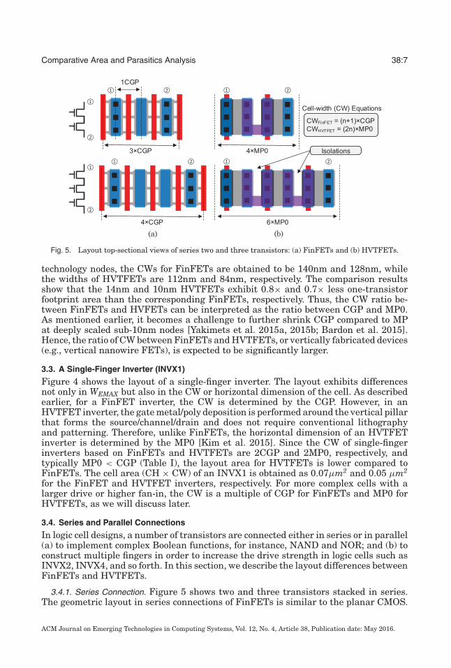
Fig. 5. Layout top-sectional views of series two and three transistors: (a) FinFETs and (b) HVTFETs.
technology nodes, the CWs for FinFETs are obtained to be 140nm and 128nm, whilethe widths of HVTFETs are 112nm and 84nm, respectively. The comparison resultsshow that the 14nm and 10nm HVTFETs exhibit 0.8× and 0.7× less one-transistorfootprint area than the corresponding FinFETs, respectively. Thus, the CW ratio be-tween FinFETs and HVFETs can be interpreted as the ratio between CGP and MP0.As mentioned earlier, it becomes a challenge to further shrink CGP compared to MPat deeply scaled sub-10nm nodes [Yakimets et al. 2015a, 2015b; Bardon et al. 2015].Hence, the ratio of CW between FinFETs and HVTFETs, or vertically fabricated devices(e.g., vertical nanowire FETs), is expected to be significantly larger.
3.3. A Single-Finger Inverter (INVX1)Figure 4 shows the layout of a single-finger inverter. The layout exhibits differencesnot only in WEMAX but also in the CW or horizontal dimension of the cell. As describedearlier, for a FinFET inverter, the CW is determined by the CGP. However, in anHVTFET inverter, the gate metal/poly deposition is performed around the vertical pillarthat forms the source/channel/drain and does not require conventional lithographyand patterning. Therefore, unlike FinFETs, the horizontal dimension of an HVTFETinverter is determined by the MP0 [Kim et al. 2015]. Since the CW of single-fingerinverters based on FinFETs and HVTFETs are 2CGP and 2MP0, respectively, andtypically MP0 < CGP (Table I), the layout area for HVTFETs is lower compared toFinFETs. The cell area (CH × CW) of an INVX1 is obtained as 0.07µm2 and 0.05 µm2
for the FinFET and HVTFET inverters, respectively. For more complex cells with alarger drive or higher fan-in, the CW is a multiple of CGP for FinFETs and MP0 forHVTFETs, as we will discuss later.
3.4. Series and Parallel ConnectionsIn logic cell designs, a number of transistors are connected either in series or in parallel(a) to implement complex Boolean functions, for instance, NAND and NOR; and (b) toconstruct multiple fingers in order to increase the drive strength in logic cells such asINVX2, INVX4, and so forth. In this section, we describe the layout differences betweenFinFETs and HVTFETs.
3.4.1. Series Connection. Figure 5 shows two and three transistors stacked in series.The geometric layout in series connections of FinFETs is similar to the planar CMOS.
ACM Journal on Emerging Technologies in Computing Systems, Vol. 12, No. 4, Article 38, Publication date: May 2016.

38:8 M. S. Kim et al.
Fig. 6. CW comparison with regard to the number of series transistors in FinFETs and HVTFET.
One diffusion region is shared between stacked transistors. Unlike stacked FinFETs,HVTFETs necessarily require shallow trench isolation (STI) [Saripalli et al. 2011;Mohata et al. 2012; Liu et al. 2013] to isolate two diffusion regions of the adjacenttransistors in order to connect the transistors in a series. This is because of the verticalnature of HVTFETs and unidirectional conduction behavior [Liu et al. 2013], as dis-cussed before. Hence, the area benefit observed in a single vertical device is no longerviable because it needs (2 × n) × MP0 for the CW while FinFETs need (n + 1) × CGP,where n is the number of series connections. For the parameters of the 14nm technologynode, the CW of each device is equal to 224nm (= 4 × 56nm) for HVFET and 210nm (=3 × 70nm) for FinFETs, respectively, when two transistors are stacked. Figure 6 de-picts the CW comparison between FinFETs and HVTFETs versus the number of seriesconnections. In two stacked transistors, the HVTFET exhibits almost the same layoutfootprint compared to FinFETs. However, the CW of HVTFET becomes wider than theCW of FinFETs due to the penalty of isolations originating from unidirectional con-duction when the number of series connections exceeds two [Kim et al. 2015]. It is alsonoted that, if the vertical FET is not asymmetric (i.e., not unidirectional conduction),which means that the current flows bidirectionally, the expression of CW for HVTFETscan be modified as (2 × n − 1) × MP0. It helps to further reduce the layout footprintby 20 ∼ 30% compared to both FinFETs and HVTFETs.
3.4.2. Parallel Connection. The layouts of transistors connected in parallel are illus-trated in Figure 7 for both FinFETs and HVTFETs. For FinFETs, the active/diffusionregions are shared between adjacent transistors, resulting in fewer diffusion breaksand a smaller area [Wang and Gupta 2014]. As an example, (n – 1) active regions wouldbe shared by adjacent transistors if n transistors are connected in parallel.
For HVTFETs in parallel, the bottom diffusion region can be shared. The sharedbottom source is connected through the via contact between two top diffusion regionswith retaining the constant MP0. Wang and Gupta [2014] introduce the compact layoutstrategy for vertical FETs, which removes the contacts between top drains. However,we keep the shared source with contacts while maintaining the MP0 between two topdrains to avoid large parasitic source resistance.
An example of three transistors connected in parallel for FinFETs and HVTFETs isshown in Figure 7. For FinFETs, the CW is equal to (n + 1) × CGP when n transistorsare connected in parallel. The CW of n parallel chains in HVTFETs is (2 × n – 1) × MP0.Figure 8 also shows the CW versus the number of parallel chains. As expected, twoparallel transistor chains in HVTFETs have less width compared to FinFETs. However,the CW of HVTFETs exceeds that of FinFETs as the number of parallel transistorsexceeds three. It is evident that the area of HVTFET-based cells will be larger thanFinFET-based cells when either the drive strength or the number of inputs increases.
ACM Journal on Emerging Technologies in Computing Systems, Vol. 12, No. 4, Article 38, Publication date: May 2016.

Comparative Area and Parasitics Analysis 38:9
Fig. 7. Layout top-sectional views of parallel two and three transistors: (a) FinFETs and (b) HVTFETs.
Fig. 8. CW comparison with regards to the number of parallel transistors in FinFETs and HVTFET.
Figure 6 and 8 show CW differences with respect to the number of parallel and seriestransistors. The CW of HVTFETs exceeds the CW of FinFETs as the number of con-nections increases due to (a) the isolation penalty for series connections and (b) contactplacement for sharing sources (or drains) for parallel transistors. In particular, theseries transistor connection has an additional isolation penalty, as discussed earlier;therefore, HVTFETs exhibit a larger area compared to FinFETs when the numberof series connections exceeds two in >20nm technology nodes and three in the 14nmtechnology node, respectively.
3.5. Area Analysis of Logic Cells in FinFETs and HVTFETsConsidering parallel and series transistor connections, the layout analysis in logiccells for the standard cell library shows an area overhead in HVTFET-based cells.Table III compares the cell width of HVTFET- and FinFET-based INV, NAND, and-or-inverter (AOI) and D flip-flop (DFF) logic gates for different drive strength anddifferent technology nodes. Above 20nm technologies, most cells (e.g., X1) based onFinFETs have area benefit compared to cells based on HVTFETs due to the isolationpenalty stemming from the asymmetric device characteristic in HVTFETs. In addition,like parallel and series transistors, the areas for HVTFETs become even worse as thenumber of inputs and drive strength increase. However, the area benefits in HVTFETsare evident from Table III for sub-20nm technology nodes. The reason is that the ratio
ACM Journal on Emerging Technologies in Computing Systems, Vol. 12, No. 4, Article 38, Publication date: May 2016.

38:10 M. S. Kim et al.
Table III. Cell-Width (CW) Changes in Comparison With FinFET-Based Cells
INV NAND AOI21 AOI22 DFFDevices X1 X2 X4 X1 X2 X1 X1 with Reset without Reset
10nm FinFET 128nm 192nm 320nm 192nm 384nm 320nm 384nm 1.41µm 1.54µmHVTFET 84nm 168nm 294nm 168nm 294nm 210nm 336nm 1.09µm 1.26µm
CW – 34% – 13% – 8.1% – 13% – 23% – 34% – 13% – 23% – 18%
14nm FinFET 140nm 210nm 350nm 210nm 420nm 350nm 420nm 1.54µm 1.68µmHVTFET 112nm 168nm 392nm 224nm 392nm 280nm 448nm 1.46µm 1.68µm
CW – 20% – 20% + 11% + 6.3% – 6.7% – 20% + 6.3% – 5.1% 0.0%
22nm FinFET 180nm 270nm 540nm 270nm 540nm 450nm 540nm 1.98µm 2.16µmHVTFET 160nm 320nm 640nm 320nm 560nm 400nm 640nm 2.08µm 2.40µm
CW – 11% + 15% + 15% + 16% + 4.0% – 11% + 15% + 4.8% + 10%∗Positive: area increases; Negative: area decreases.
Fig. 9. Modeling of geometry-dependent parasitic components with ideal core model.
between MP0 and CGP decreases (e.g., MP0/CGP = 0.9 for 22nm, 0.8 for 14nm, and0.7 for 10nm). It leads to reduction of the CW in HVTFET-based cells.
4. EXTRACTIONS OF PARASITICS IN FINFETS AND HVTFETSAs technology is continuously scaling, the fabrication process is becoming dense andmore complicated. Consequently, the parasitic resistive and capacitive componentsbecome comparable to, and even larger than, the intrinsic resistive and capacitivecomponents [Pacha et al. 2006]. This parasitic resistance results in a significant degra-dation of current drive capability, leading to the severe degradation of performance inlogic cells. The parasitic capacitances may dominate the intrinsic device characteris-tics in analog/RF systems [Pacha et al. 2006; Wu and Chan 2007]. Also, in the digitaldomain, these parasitics lead to the degradations of speed and power efficiency due toincreased capacitance and reduced ION [Wu and Chan 2007; Wei et al. 2009]. Hence,in order to perform accurate power and timing analysis through the synthesis flow inlogic cells, it is crucial to capture parasitic resistance and capacitance originating fromgeometry-dependent device structure.
In the following section, we describe the analytically estimated parasitics appendedto an ideal device core model [Liu et al. 2013], as illustrated in Figure 9. Note that theparasitics until the metal 0 trench contact (M0A) are evaluated and the parasitics ofupper-trench contacts are ignored since this article focuses on parasitics originatingfrom the differences among device structures rather than interconnect parasitics.
4.1. Basic Capacitive Component ModelingThe parasitic capacitances in FinFETs have already been analyzed in a numberof articles [Wu and Chan 2007; Salas Rodriguez et al. 2013; Bhoj et al. 2013]. Amultigate FinFET structure entails significant attention to the newly formed parasitic
ACM Journal on Emerging Technologies in Computing Systems, Vol. 12, No. 4, Article 38, Publication date: May 2016.
Comparative Area and Parasitics Analysis 38:11
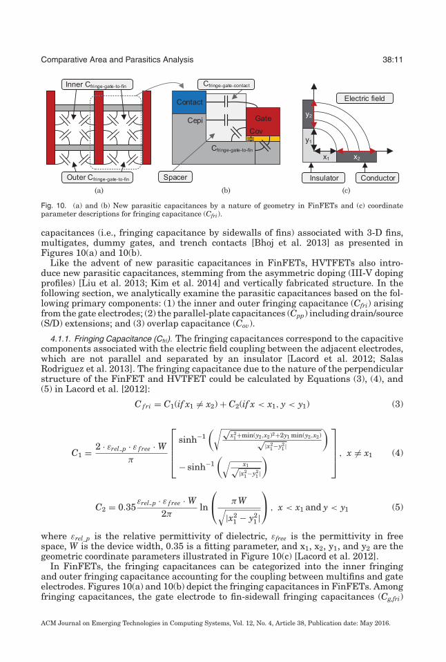
Fig. 10. (a) and (b) New parasitic capacitances by a nature of geometry in FinFETs and (c) coordinateparameter descriptions for fringing capacitance (Cfri).
capacitances (i.e., fringing capacitance by sidewalls of fins) associated with 3-D fins,multigates, dummy gates, and trench contacts [Bhoj et al. 2013] as presented inFigures 10(a) and 10(b).
Like the advent of new parasitic capacitances in FinFETs, HVTFETs also intro-duce new parasitic capacitances, stemming from the asymmetric doping (III-V dopingprofiles) [Liu et al. 2013; Kim et al. 2014] and vertically fabricated structure. In thefollowing section, we analytically examine the parasitic capacitances based on the fol-lowing primary components: (1) the inner and outer fringing capacitance (Cfri) arisingfrom the gate electrodes; (2) the parallel-plate capacitances (Cpp) including drain/source(S/D) extensions; and (3) overlap capacitance (Cov).
4.1.1. Fringing Capacitance (Cfri). The fringing capacitances correspond to the capacitivecomponents associated with the electric field coupling between the adjacent electrodes,which are not parallel and separated by an insulator [Lacord et al. 2012; SalasRodriguez et al. 2013]. The fringing capacitance due to the nature of the perpendicularstructure of the FinFET and HVTFET could be calculated by Equations (3), (4), and(5) in Lacord et al. [2012]:
C fri = C1(if x1 = x2) + C2(if x < x1, y < y1) (3)
C1 = 2 · εrel p · ε f ree · Wπ
⎡
⎢⎢⎢⎣
sinh−1(√√
x21+min(y2,x2)2+2y1 min(y2,x2)√
|x21−y2
1 |
)
− sinh−1(√ x1√
|x21−y2
1 |
)
⎤
⎥⎥⎥⎦, x = x1 (4)
C2 = 0.35εrel p · ε f ree · W
2πln
⎛
⎝ πW√
|x21 − y2
1 |
⎞
⎠ , x < x1 and y < y1 (5)
where εrel_p is the relative permittivity of dielectric, εfree is the permittivity in freespace, W is the device width, 0.35 is a fitting parameter, and x1, x2, y1, and y2 are thegeometric coordinate parameters illustrated in Figure 10(c) [Lacord et al. 2012].
In FinFETs, the fringing capacitances can be categorized into the inner fringingand outer fringing capacitance accounting for the coupling between multifins and gateelectrodes. Figures 10(a) and 10(b) depict the fringing capacitances in FinFETs. Amongfringing capacitances, the gate electrode to fin-sidewall fringing capacitances (Cg,fri)
ACM Journal on Emerging Technologies in Computing Systems, Vol. 12, No. 4, Article 38, Publication date: May 2016.

38:12 M. S. Kim et al.
Fig. 11. The parasitic capacitance in HVTFETs. (a) Front, (b) side, and (c) consideration of tapered shape.
dominate other fringing capacitances because of a relatively large dimension of theHFIN in FinFETs [Lacord et al. 2012; Salas Rodriguez et al. 2013].
Figures 11(a) and 11(b) illustrate the fringing capacitances (Cfri) in HVTFETs. Sim-ilar to FinFETs, the fringing capacitance between the gate electrode and the verticalpillar (S/D) can be calculated by Equations (3), (4), and (5). Note that the Cfri (e.g.,Cgd,fri_side, Cgs,fri_side, Cds,fri_gext, and Cgs,fri_gext) and Cpp (e.g., Cgs,ext and Cgd,ext) are dou-bled in HVTFETs due to the vertical pillar structure and double gate.
4.1.2. Parallel-Plate Capacitance (Cpp). Among parasitic capacitances, one of the primarycapacitance sources is the parallel-plate capacitance. These components are calculatedby using Equation (6) with an assumption of perfect parallel-plates:
Cpp = (εrel p · ε f ree)A/d, (6)
where A is the area of parallel plate and d is the distance between the plates. InFinFETs, the primary parallel-plate components are the capacitances between gateand S/D diffusion region (CEpi) along the sidewall and along the top of fins (CEpi-top).These capacitances can be calculated using Equation (6), relative permittivity of high-kspacer (e.g., εrel_p = εspacer = 5.5 in this article [Yakimets et al. 2015a]), and thicknessof spacer between the gate electrode and S/D diffusion regions.
Figure 11(a) shows various parallel-plate capacitances in HVTFETs. Two major com-ponents of the parallel-plate capacitance is Cgd,ext and Cgs,ext between S/D electrodeextensions and gate electrodes. Further, there is an additional via required to connectthe bottom extension source. This additional connection introduces a new parasiticcapacitance between the gate electrode and the via. Here, we employ the conventionaldiscrete via implementation process [Lacord et al. 2012]. This parasitic capacitance,Cgs,via, between the gate electrode along the sidewall and via can be simply expressedusing corresponding Equation (7) for a parallel-plate capacitor:
Cgs,via = Nvia · Wvia · (Lg + Lov) · εILD · ε f ree/Tsp, (7)
where Nvia is the number of vias along WEMAX, Wvia is the width of a via, Lov is theoverlap length derived from the penetration to S/D regions beneath the gate, Tsp is thedistance between a gate electrode to a via, and εILD and εfree_space are the permittivityfor interlayer dielectric and free space, respectively.
Equation (7) can be used when a via and gate electrode are perfectly rectangular-shaped. However, in general, devices have a tapered shape rather than rectangular, asshown in Figure 11(c). Hence, we modify Equation (7) to (8) with respect to an angle in
ACM Journal on Emerging Technologies in Computing Systems, Vol. 12, No. 4, Article 38, Publication date: May 2016.

Comparative Area and Parasitics Analysis 38:13
Fig. 12. (a) Geometry parameters for overlap capacitance (a) Lov, (b) FinFET, and (c) HVTFETs.
θ (Figure 11(c)). Here, we assume that θ is the same for angles of the gate and via.
Cgs,via(θ ) = Nvia ·Wvia ·sin θ ·(Lg+2·Lov)· εILD · ε f ree
MP0 −(
12 Tb + Tox + Tgate + Wvia−Hvia/ tan θ
2
) (8)
If θ is 80 and employing the device parameters (e.g., Tox = 2nm, Tb = 7nm, Tgate =5nm, Wvia = 15nm, and Hvia = 105nm) of HVTFETs [Liu et al. 2014] and processparameters of the 14nm node, Cgs,via in HVTFETs is equal to 0.34 aF/via. This parasiticcapacitance originating from the additional vias increases as the feature dimensionsreduce in accordance with technology scaling. Other capacitances components such asthe WE-dependent Cpp, Cfri, and Cov decrease due to reduction of WE at a fixed CH (i.e.,from WE = 380nm at the 22nm node to WE = 268nm at the 14nm node (Figure 4)).
4.1.3. Overlap Capacitance. The overlap capacitance (Cov) originates from the overlapbetween S/D regions and the gate, as shown in Figure 12(a). Cov includes the gate-source lateral extension overlap capacitance along the sidewall Cgs1,ov, and Cgs2,ov andthe gate-drain overlap capacitance Cgd1,ov and Cgd2,ov [Liu et al. 2013]. Lov of 1nm isemployed from the edge of the gate electrode to the S/D region [Liu et al. 2013] for eachdevice. Since the traditional calculation based on parallel-plate capacitor concept is notappropriate to FinFETs due to the finite thickness of the gate and S/D region [Wu andChan 2007], the expression for Cov is derived by considering a tri-gate structure andusing equations in Wu and Chan [2007]:
Cov = NF IN · (2TF IN + 4HF IN) · cov(Tox), (9)
where cov(u) = %(u)+Lov
u εox + 2εSiπ
ln[1 + xju sin(k)], k = π
2 · εoxεSi
, %(u) = u2 [1 + 1−cos(k)
sin(k) )], and xj
is the junction depth and assumed to TFIN/2 for 2TFIN term and HFIN/2 for 4HFIN term[Wu and Chan 2007]. The εox and εSi denote the dielectric constant for the gate oxideand silicon, respectively. For HVTFETs, there are two components of Cov originatingfrom the asymmetric structure and different doping profiles (e.g., GaSb and InAs) ofS/D regions, unlike FinFETs. The Cov can be modified by using Equation (9) consideringthe ultra-thin-body (UTB) vertical structure of HVTFETs:
Cov =[
2Tb · cov(TMask, WEMAX/4)+WEMAX · cov(Tox, Tb/2)
]
InAs+
[2Tb · cov(TMask, WEMAX/4)+WEMAX · cov(Tox, Tb/2)
]
GaSb, (10)
where cov(u, v) = %(u)+Lov
u εox + 2εGaSb,εInAsπ
ln[1 + vu sinkGaSb, kInAs], k = π
2 · εoxεGaSb,εInAs ,
%(u) = u2 [1 + 1−coskGaSb,kInAs
sinkGaSb,kInAs ]. The εGaSb = 15.7 and εInAs = 15.1 indicate each dielectricconstant for the GaSb and InAs in HVTFETs [Liu et al. 2013], respectively.
Applying device parameters in Liu et al [2013] and WEMAX in Figure 4 reveals thatCov in HVTFETs is 28.0% larger than FinFETs in 22nm node (e.g., 40.2 aF for FinFETsand 51.5 aF for HVTFETs). However, in 14nm node, Cov in HVTFETs become less than
ACM Journal on Emerging Technologies in Computing Systems, Vol. 12, No. 4, Article 38, Publication date: May 2016.

38:14 M. S. Kim et al.
Fig. 13. The overall capacitance breakdown in different technology nodes: different device width at a givencell height (Figure 4).
Fig. 14. The parasitic capacitance comparison based on the 14nm technology: (a) FinFET and (b) HVTFET.
FinFETs at a given WEMAX (e.g., 39.7 aF for FinFETs and 36.9 aF for HVTFETs).HVTFETs exhibit larger reduction in Cov compared to FinFETs as technology scalesbecause WE scales to a larger extent from the 22nm node to the 14nm node (Figure 4).
4.1.4. Parasitic Capacitance versus Gate Channel Capacitance. As CGP scales with technol-ogy, the parasitic capacitance (Cpar) becomes comparable and may even exceed the gatechannel capacitance (Cg) in FinFETs. The portion of Cpar with respect to Cg increasesfurther due to the reduced FP and higher HFIN at the advanced technology nodes, asdescribed in Figure 1. This trend is also shown in Figures 13 and 14(a), which illustratethe ratio of Cpar and Cg at different technology nodes. At the 14nm node, for example,Cpar is 66% of the total capacitance (Ctot), for which the WE is 276nm.
Figures 13 and 14(b) show the capacitance breakdown for HVTFETs. In contrast toFinFETs, the Ctot, including intrinsic gate channel capacitance and parasitic capaci-tances, decreases in accordance with shrinking MP0. This is the reason that the Cfri,Cpp, and Cov decrease accordingly because the WE decreases (Figure 4) when the tech-nology node moves from 22nm to 14nm with the reduced CH in nanometers (e.g., FP ×10). For the ratio between Cpar and Cg, as presented in Figure 13, the Cpar is 62% ofthe Ctot, showing a similar result to FinFETs in the 14nm technology.
As shown in Figure 14, Cpar exceeds over the Cg in both FinFET and HVTFETs.Two devices exhibit different percentages of fractions in the total capacitance. ForFinFETs, fringing and parallel-plate capacitances are the dominant components of theCtot because of the 3-D fin structure. On the other hand, for HVTFETs, the contributionsof the fringing, parallel-plate, and overlap capacitances are almost even.
ACM Journal on Emerging Technologies in Computing Systems, Vol. 12, No. 4, Article 38, Publication date: May 2016.

Comparative Area and Parasitics Analysis 38:15
Fig. 15. The parasitic resistance modeling from device structures: (a) FinFET and (b) HVTFET (Note: Gateresistance (Rgext) is not shown).
4.2. Basic Resistive Component ModelingParasitic resistance (Rpar) extraction is always a trade-off between accuracy and com-puting resources. As processes become denser, finding a trade-off is becoming moredifficult because the process is becoming more complex and the number of gates is in-creasing. In this section, we discuss key parasitic resistances that lead to the significantdegradation of ION.
There are two primary parasitic resistances: (1) gate resistance and (2) S/D seriesresistances. The gate parasitic resistance and capacitances (Section 4.1) are criticalin determining the gate resistance–capacitance (RC) delay [Wu and Chan 2007]. S/Dparasitic resistance is also a crucial factor to determine the ION degradation comparedto the ideal core device model without parasitics.
The main difference in the parasitic resistance of FinFETs and HVTFETs is that,unlike FinFETs, HVTFETs exhibit unequal source and drain resistances (Rs and Rd,respectively). The symmetric structure of FinFETs leads to the same parasitic resis-tances on the source and drain sides. However, unlike FinFETs, additional via requiredto place contacts on the bottom active region, asymmetric doping profile, and differentheights of S and D pillars in HVTFETs lead to unequal Rs and Rd. In this section, weexplore the parasitic resistances in HVTFETs and compare the parasitic resistancesacross FinFETs and HVTFETs.
4.2.1. Analysis of Parasitic Resistance in Device Structures. Figure 15 presents the parasiticresistances in the FinFET and HVTFET. For sake of simplicity, we assume that allregions have perfect rectangular shapes.
In FinFETs, the Rpar due to the contact placement (both silicide and trench contact(M0A)), epitaxial diffusion region, and extension of the fin and gate are considered aspresented in Figure 15. All geometry parameters are based on Table I and the contactmaterial is assumed as tungsten (W). Also, the parameters of Silicon (Si) and SiGerelated to the resistance are used for n- and p-type FinFETs, respectively.
HVTFETs also have the contact resistance (Rcon) and S/D extension resistance (Rdextor Rsext). Further, the additional parasitic resistances, such as the bottom diffusionextension for the contact (Rsel,ext) and via resistance (Rvia), are also considered since oneof diffusion area (source or drain) is placed on the bottom, resulting in an additionalvia implementation on the bottom diffusion region, as mentioned earlier. The samegeometry parameters and contact material are used. Other parameters related to thematerials (i.e., resistivity, doping level, work function, and so forth) are based on Liuet al. [2013].
All resistances are calculated by Equation (11) with the resistivity of numerousmaterials if all regions corresponding to the device structures have perfect rectangular
ACM Journal on Emerging Technologies in Computing Systems, Vol. 12, No. 4, Article 38, Publication date: May 2016.

38:16 M. S. Kim et al.
Fig. 16. The parasitic resistance comparison based on the 14nm technology: (a) FinFET and (b) HVTFET.
shapes:
Resistance[&] = (ρ · L)/A, (11)
where ρ is the resistivity of a material, A is the orthogonal area related to the currentpath, and L is the length of the current route. The via resistance, Rvia, for instance,depends on the dimensions (e.g., via size and height) and resistivity of the tungstenof the via. With an assumption of 15 × 15nm via cross-sectional area in 14nm node[Natarajan et al. 2014], the Rvia and Rsilicide are calculated as 21.86 Ω and 85.43 Ω,respectively.
Figure 16 summarizes the parasitic resistances for both FinFETs and HVTFETs. InFinFETs, the major components in the overall parasitic resistance are S/D extensionresistance due to the thin body of fins and contact resistances, which are 49% and 28%of the total parasitic resistance, respectively. In HVTFETs, Rd is much larger thanother parasitic components since HVTFETs have a longer drain pillar as opposed to ashorter source pillar due to the asymmetric doping [Liu et al. 2012].
The HVTFET requires a higher doping source to enable more tunneling current anda lighter doping drain to reduce the leakage current (e.g., the tunneling from drain-channel-source due to the unbipolar transport). Hence, the junction line (channel drain)at the drain side will be pushed toward the drain contact more. In this case, a longerdrain for HVTFETs is necessary to ensure that the drain depletion region is still withinthe device [Rajamohanan et al. 2013; Liu et al. 2012]. Due to a large Rd from Figure 16,the ratio of Rd and Rs is 60% and 37% even with Rsel,ext and Rvia.
4.3. Parasitics by Series and Parallel ConnectionsSimilar to the analysis of impact of different device architectures on the layout that wepresented in Section 3, the analysis of the effect of parasitics in logic gates with seriesand parallel transistors is also crucial.
4.3.1. Series Connections. As discussed in Section 2, HVTFETs exhibit unidirectionalconduction, originating from the asymmetric doping and p-i-n device structure. Becauseof this behavior, isolation is necessary to separate two transistors. This isolation resultsin an additional parasitic capacitance arising from the STI between HVTFETs whenthey are connected in a series (Figure 5 in series). Hence, increasing the number ofseries connections increases the parasitic capacitances compared to FinFETs. However,this capacitance originating from STI is not a prominent portion relative to otherparasitic components due to fairly wide MP0 compared to other feature parameters.Therefore, the total capacitance and resistance can be calculated by the number ofseries transistors times the parasitics, resulting in more total parasitics than FinFETs,
ACM Journal on Emerging Technologies in Computing Systems, Vol. 12, No. 4, Article 38, Publication date: May 2016.

Comparative Area and Parasitics Analysis 38:17
Fig. 17. The parasitic capacitance and resistance with a number of series transistors.
as shown in Equation (12) and Figure 17.
Rtot-par(n),FinFET = Rpar,FinFET + (n − 1) · (Repi + Rsext) ≈ n · Rpar,FinFETCtot-par(n),FinFET = 0.5(n + 1) · Cpar − n · C fringe-gate-contact
Rtot-parasitic(n),HVTFET = n · Rpar,HVTFETCtot-par(n),HVTFET = n · Cpar
, (12)
where Rtot-par and Ctot-par are the total parasitic resistance and capacitance, and n isthe number of transistor connections.
Unlike HVTFETs, FinFETs share a diffusion region between two gate electrodes inseries, resulting in less parasitics than HVTFETs. As the number of series connectionsincreases, additional parasitic capacitances by 1 × CGP are added, equal to 3 F ×(inner fringing capacitance and outer fringing capacitance) + (1 × Cfringe-gate-contact)+ CEpi. For resistance, since one diffusion area is shared, half of the total parasiticresistance in a single-finger FinFET is added when the number of series connectionsincreases.
The parasitic capacitance and resistance in series connections are presented in Fig-ure 17. When the number of series connections exceeds 2, the total parasitic capacitancein HVTFETs becomes larger than FinFETs. In addition, the total parasitic resistancein HTFETs is always worse than FinFETs because of (a) unique geometry structure(e.g., asymmetric pillar heights for each source and drain) [Mohata et al. 2012], (b) elec-trical parameters (e.g., resistivity) [Liu et al. 2013], and (c) isolation between activearea [Liu et al. 2013] in HVTFETs, especially for a larger number of series transistorconnections.
ACM Journal on Emerging Technologies in Computing Systems, Vol. 12, No. 4, Article 38, Publication date: May 2016.
38:18 M. S. Kim et al.
Fig. 18. The parasitic capacitance and resistance with a number of parallel transistors.
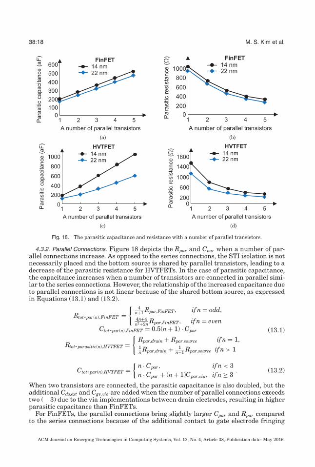
4.3.2. Parallel Connections. Figure 18 depicts the Rpar and Cpar when a number of par-allel connections increase. As opposed to the series connections, the STI isolation is notnecessarily placed and the bottom source is shared by parallel transistors, leading to adecrease of the parasitic resistance for HVTFETs. In the case of parasitic capacitance,the capacitance increases when a number of transistors are connected in parallel simi-lar to the series connections. However, the relationship of the increased capacitance dueto parallel connections is not linear because of the shared bottom source, as expressedin Equations (13.1) and (13.2).
Rtot-par(n),FinFET = 4
n+1 Rpar,FinFET, if n = odd,
4n+4n2+2n Rpar,FinFET, if n = even
Ctot-par(n),FinFET = 0.5(n + 1) · Cpar
Rtot-parasitic(n),HVTFET =
Rpar,drain + Rpar,source if n = 1,1n Rpar,drain + 1
n−1 Rpar,source if n > 1
(13.1)
Ctot-par(n),HVTFET =
n · Cpar, if n < 3n · Cpar + (n + 1)Cpar,via, if n ≥ 3
. (13.2)
When two transistors are connected, the parasitic capacitance is also doubled, but theadditional Cds,ext and Cgs,via are added when the number of parallel connections exceedstwo (! 3) due to the via implementations between drain electrodes, resulting in higherparasitic capacitance than FinFETs.
For FinFETs, the parallel connections bring slightly larger Cpar and Rpar comparedto the series connections because of the additional contact to gate electrode fringing
ACM Journal on Emerging Technologies in Computing Systems, Vol. 12, No. 4, Article 38, Publication date: May 2016.
Comparative Area and Parasitics Analysis 38:19
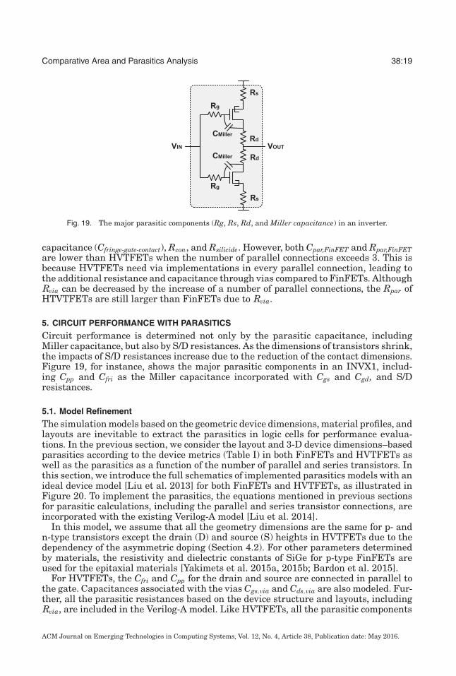
Fig. 19. The major parasitic components (Rg, Rs, Rd, and Miller capacitance) in an inverter.
capacitance (Cfringe-gate-contact), Rcon, and Rsilicide. However, both Cpar,FinFET and Rpar,FinFETare lower than HVTFETs when the number of parallel connections exceeds 3. This isbecause HVTFETs need via implementations in every parallel connection, leading tothe additional resistance and capacitance through vias compared to FinFETs. AlthoughRvia can be decreased by the increase of a number of parallel connections, the Rpar ofHTVTFETs are still larger than FinFETs due to Rvia.
5. CIRCUIT PERFORMANCE WITH PARASITICSCircuit performance is determined not only by the parasitic capacitance, includingMiller capacitance, but also by S/D resistances. As the dimensions of transistors shrink,the impacts of S/D resistances increase due to the reduction of the contact dimensions.Figure 19, for instance, shows the major parasitic components in an INVX1, includ-ing Cpp and Cfri as the Miller capacitance incorporated with Cgs and Cgd, and S/Dresistances.
5.1. Model RefinementThe simulation models based on the geometric device dimensions, material profiles, andlayouts are inevitable to extract the parasitics in logic cells for performance evalua-tions. In the previous section, we consider the layout and 3-D device dimensions–basedparasitics according to the device metrics (Table I) in both FinFETs and HVTFETs aswell as the parasitics as a function of the number of parallel and series transistors. Inthis section, we introduce the full schematics of implemented parasitics models with anideal device model [Liu et al. 2013] for both FinFETs and HVTFETs, as illustrated inFigure 20. To implement the parasitics, the equations mentioned in previous sectionsfor parasitic calculations, including the parallel and series transistor connections, areincorporated with the existing Verilog-A model [Liu et al. 2014].
In this model, we assume that all the geometry dimensions are the same for p- andn-type transistors except the drain (D) and source (S) heights in HVTFETs due to thedependency of the asymmetric doping (Section 4.2). For other parameters determinedby materials, the resistivity and dielectric constants of SiGe for p-type FinFETs areused for the epitaxial materials [Yakimets et al. 2015a, 2015b; Bardon et al. 2015].
For HVTFETs, the Cfri and Cpp for the drain and source are connected in parallel tothe gate. Capacitances associated with the vias Cgs,via and Cds,via are also modeled. Fur-ther, all the parasitic resistances based on the device structure and layouts, includingRvia, are included in the Verilog-A model. Like HVTFETs, all the parasitic components
ACM Journal on Emerging Technologies in Computing Systems, Vol. 12, No. 4, Article 38, Publication date: May 2016.

38:20 M. S. Kim et al.
Fig. 20. The parasitic elements modeling in the schematic view: (a) FinFETs and (b) HVTFETs.
Fig. 21. Delay and energy comparison in 15-stage RO without/with parasitics.
induced by the geometric device structure, number of fins and layouts are incorporatedexcept the parasitics from the not-self-aligned vias in FinFETs.
5.2. Ring Oscillator (RO)–Based Benchmarking.For the benchmarking, we use the 15-stage INVX1-based RO with parasitics discussedearlier but ignore those due to interconnections. In order to analyze the impacts ofparasitics, the simulations are performed using models with and without the deviceparasitics in SPICE. All the CHs of INVX1 are set to 7.5 T based on the metal pitch asdescribed in Section 2.
Figure 21 shows the delay and energy comparisons without and with parasiticsfor FinFET and HVTFET [Liu et al. 2013] based on geometric parameters in 14nmtechnology node (Table I) at multiple supply voltages. At a 14nm technology node,the electrical width is set to 276nm for FinFETs and 268nm for HVTFETs for eachp- and n-type transistor, as shown in Figure 4. For comparisons, the delay and energy
ACM Journal on Emerging Technologies in Computing Systems, Vol. 12, No. 4, Article 38, Publication date: May 2016.

Comparative Area and Parasitics Analysis 38:21
cross-over point is observed near 0.45V. Below this point, HVTFETs outperformFinFETs even with smaller WE because of the larger current driving ability (high ION)stemming from steep-slope switching [Mohata et al. 2012; Liu et al. 2013]. However,over 0.45V, FinFETs can provide better performance due to higher current drivingability of FinFETs at a higher VDD [Mohata et al. 2012; Liu et al. 2013]. The parasiticslead to an approximately 20% delay degradation in HVTFETs. The delay increasein FinFET-based cells because of parasitics is less than 12%. The larger degradationof delay in HVTFETs compared to FinFETs is due to (a) an increase in parasiticcapacitances, mainly Cfri and Cpp, and (b) relatively higher parasitic resistance (Rsand Rd) plus the bottom diffusion area extension (Rsel,ext + Rvia) for the vias.
The energy comparison is shown in Figure 20(b). The FinFETs have not only largerWE but also the 1.2× higher total capacitances, including intrinsic and parasitic, thanHVTFETs, resulting in higher energy compared to HVTFETs [Liu et al. 2012, 2013].Further, for the evaluation with parasitics, as presented in Figure 13, the parasiticcapacitances in FinFETs are also more than HVTFETs, leading to 36% higher energy.Figure 20(b) shows that energy efficiency degrades approximately 47% with parasiticsat various VDDs compared to the results without parasitics.
6. CONCLUSIONIn this article, we have examined the layout implications of the asymmetric verticalheterojunction tunnel FET (HVTFET) compared to FinFETs for a standard cell librarywith a fixed height of 7.5 × metal 2 pitch (7.5 T). The benefits and trade-offs in thelayout analysis are also investigated by considering parallel and series transistor con-nections based on the Boolean function implementations in logic cells. In addition, thedevice parasitics are explored for both FinFETs and HVTFETs. The total parasitics inHVTFETs and FinFETs are compared with various technology dimensions. Also, theparasitics related to series and parallel transistor connections are evaluated to explorethe benefits and trade-offs in the logic cells. In this analysis, the parasitic capacitanceof one transistor is lower than FinFETs. However, the parasitic capacitance increasessignificantly with more series or parallel transistor connections. In most cases, morethan two transistor connections exhibit more parasitic capacitance. For parasitic re-sistances, HVTFETs always show more parasitics than FinFETs due to high drainpillar resistance and additional Rvia. Further, in order to investigate the impacts oncircuit performance, we have incorporated the parasitic capacitance and resistance in aVerilog-A model, and examined the impacts of parasitics in the 15-stage ring oscillator.Based on the benchmarking, although HVTFETs have more performance degradationwith parasitics, HVTFETs still can provide higher energy efficiency at various supplyvoltages (0.3V–0.7V) than FinFETs.
ACKNOWLEDGMENTS
The authors would like to thank Dr. Huichu Liu at Intel Corporation for providing specifications about thedimensions in Lg = 20nm HVTFETs.
REFERENCESM. Alioto. 2011. Comparative evaluation of layout density in 3T, 4T, and MT FinFET standard cells. IEEE
Transactions on Very Large Scale Integration Systems 19, 5, 751–762. DOI:10.1109/TVLSI.2010.2040094K. G. Anil et al. 2003. Layout density analysis of FinFETs. 33rd Conference on European Solid-State Device
Research. DOI:10.1109/ESSDERC.2003.1256830M. G. Bardon et al. 2015. Dimensioning for power and performance under 10nm: The limits of Fin-
FETs scaling. International Conference on IC Design and Technology (ICICDT’15). DOI:10.1109/ICICDT.2015.7165883
ACM Journal on Emerging Technologies in Computing Systems, Vol. 12, No. 4, Article 38, Publication date: May 2016.
38:22 M. S. Kim et al.
A. N. Bhoj et al. 2013. 3-D-TCAD-based parasitic capacitance extraction for emerging multigate de-vices and circuits. IEEE Transactions on Very Large Scale Integration Systems 21, 11, 2094–2105.DOI:10.1109/TVLSI.2012.2227848
A. Biddle and Jason S. T. Chen. 2013. FinFET technology – understanding and productizing a new transistor.A Joint Whitepaper from TSMC and Synopsys.
Y. K. Choi et al. 2001. Sub-20 nm CMOS FinFET technologies 2001. International Electron Devices Meeting,(IEDM’01). 19.1.1–19.1.4, 2–5. DOI:10.1109/IEDM.2001.979526
T. Cui et al. 2014. 7nm FinFET standard cell layout characterization and power density prediction in near-and super-threshold voltage regimes. International Green Computing Conference (IGCC’14).
S. Datta et al. 2013. Tunnel transistors for energy efficient computing. IEEE International Reliability PhysicsSymposium (IRPS’13). DOI:10.1109/IRPS.2013.6532046
F. He et al. 2010. FinFET: From compact modeling to circuit performance. IEEE International Conferenceon Electron Devices and Solid-State Circuits (EDSSC’10). DOI:10.1109/EDSSC.2010.5713788
U. Heo et al. 2015. A high-efficiency switched-capacitance HTFET charge pump for low-input-voltage appli-cations. In IEEE VLSI Design. DOI:10.1109/VLSID.2015.58
C. Hou et al. 2013. TSMC Technology Symposium 2013: Progress in 20nm, 16nm FinFET, and 3D-ICTechnologies. Retrieved April 18, 2016 from http://community.cadence.com/cadence_blogs_8/b/ii/archive/2013/04/14/tsmc-2013-symposium-progress-in-20nm-16nm-finfet-and-3d-ic-technologies.
C. H. Jan et al. 2012. A 22nm SoC platform technology featuring 3-D tri-gate and high-k/metal gate, optimizedfor ultra low power, high performance and high density SoC applications. IEEE International ElectronDevices Meeting (IEDM’12). DOI:10.1109/IEDM.2012.6478969
M. S. Kim et al. 2014. A steep-slope tunnel FET based SAR analog-to-digital converter. IEEE Transactionson Electron and Devices 61, 11. DOI:10.1109/TED.2014.2359663
M. S. Kim et al. 2014. Enabling power-efficient designs with III-V tunnel FETs. IEEE Compound Semicon-ductor Integrated Circuit Symposium (CSICs’14). DOI:10.1109/CSICS.2014.6978551
M. S. Kim et al. 2015. Comparing energy, area, delay tradeoffs in going vertical with CMOS and asym-metric HTFETs. In IEEE Computer Society Annual Symposium on VLSI (ISVLSI’15). Montpellier.DOI:10.1109/ISVLSI.2015.82
K. J. Kuhn et al. 2010. Technology options for 22nm and beyond. 2010 International Workshop on JunctionTechnology (IWJT’10). DOI:10.1109/IWJT.2010.5475000
K. J. Kuhn. 2012. Considerations for ultimate CMOS scaling. IEEE Transactions on Electron Devices 59, 7,1813–1828.
J. Lacord, G. Ghibaudo, and F. Boeuf. 2012. Comprehensive and accurate parasitic capacitance models fortwo- and three-dimensional CMOS device structures. IEEE Transactions on Electron Devices 59, 5,1332–1344. DOI:10.1109/TED.2012.2187454
H. Liu et al. 2012. Exploration of vertical MOSFET and tunnel FET device architecture for sub-10nm nodeapplications. Annual Device Research Conference (DRC’12). DOI:10.1109/DRC.2012.6256990
H. Liu, S. Datta, and V. Narayanan. 2013. Steep switching tunnel FET: A promise to extend the energyefficient roadmap for post-CMOS digital and analog/RF applications. IEEE International Symposiumon Low Power Electronics and Design (ISLPED’13). DOI:10.1109/ISLPED.2013.6629285
H. Liu et al. 2014. III-V Tunnel FET Model 1.0.1. Retrieved April 18, 2016 from https://nanohub.org/publications/12.
H. Liu et al. 2014. Tunnel FET RF rectifier design for energy harvesting applications. IEEE Journal onEmerging and Selected Topics in Circuits and Systems 4, 4, 400, 411.
D. K. Mohata et al. 2012. Demonstration of improved heteroepitaxy, scaled gate stack and reduced inter-face states enabling heterojunction tunnel FETs with high drive current and high on-off ratio. 2012Symposium on VLSI Technology (VLSIT’12). DOI:10.1109/VLSIT.2012.6242457
S. Natarajan et al. 2014. A 14nm logic technology featuring 2nd-generation FinFET, air-gapped interconnects,self-aligned double patterning and a 0.0588 µm2 SRAM cell size. In IEEE International Electron DevicesMeeting (IEDM’14), 3.7.1–3.7.3, 15–17. DOI:10.1109/IEDM.2014.7046976
C. Pacha et al. 2006. Circuit design issues in multi-gate FET CMOS technologies. IEEE International Solid-State Circuits Conference (ISSCC’06). DOI:10.1109/ ISSCC.2006.1696221
B. Rajamohanan et al. 2013. Low-temperature atomic-layer-deposited high-k dielectric for p-ChannelIn0.7Ga0.3As/GaAs0.35Sb0.65 heterojunction tunneling field-effect transistor. Applied Physics Express.
S. Salas Rodriguez et al. 2013. Parasitic gate capacitance model for triple-gate FinFETs. IEEE Transactionson Electron Devices. DOI:10.1109/TED.2013.2282629
V. Saripalli et al. 2011. Exploiting heterogeneity for energy efficiency in chip multiprocessors. IEEE Journalon Emerging and Selected Topics in Circuits and Systems. DOI:10.1109/JETCAS.2011.2158343
ACM Journal on Emerging Technologies in Computing Systems, Vol. 12, No. 4, Article 38, Publication date: May 2016.

Comparative Area and Parasitics Analysis 38:23
A. C. Seabaugh and Q. Zhang. 2010. Low-voltage tunnel transistors for beyond CMOS Logic. In Proceedingsof the IEEE 98, 12, 2095–2110. DOI:10.1109/JPROC.2010.2070470
K. Swaminathan et al. 2014. Steep slope devices: Enabling new architectural paradigms. Design AutomationConference (DAC’14). DOI:10.1109/DAC.2014.6881441
S. E. Thompson et al. 2005. In search of “Forever,” continued transistor scaling one new material at a time.In IEEE Transactions on Semiconductor Manufacturing. DOI:10.1109/TSM.2004.841816
W. C. Wang and P. Gupta. 2014. Efficient layout generation and evaluation of vertical channel devices.IEEE/ACM ICCAD’14. DOI:10.1109/ICCAD.2014.7001404
L. Wei, F. Boeuf, T. Skotnicki, and H. S. P. Wong. 2009. CMOS technology roadmap projection includingparasitic effects. VLSI-TSA. DOI:10.1109/VTSA.2009.5159299
W. Wu and M. Chan. 2007. Analysis of geometry-dependent parasitics in multifin double-gate FinFETs.IEEE Transactions on Electron Devices. DOI:10.1109/TED.2007.891252
Q. Xie et al. 2014. 5nm FinFET standard cell library optimization and circuit synthesis in near-and super-threshold voltage regimes. ISVLSI’14. DOI:10.1109/ISVLSI.2014.101
D. Yakimets et al. 2015a. Vertical GAAFETs for the ultimate CMOS scaling. IEEE Transactions on ElectronDevices 62, 5, 1433–1439. DOI:10.1109/TED.2015.2414924
D. Yakimets et al. 2015b. Lateral NWFET optimization for beyond 7nm nodes. International Conference onIC Design and Technology (ICICDT’15), 1–4, 1–3. DOI:10.1109/ICICDT.2015.7165887
B. Yu et al. 2002. FinFET scaling to 10 nm gate length. International Electron Devices Meeting (IEDM’02).251–254. DOI:10.1109/IEDM.2002.1175825
Received September 2015; revised March 2016; accepted April 2016
ACM Journal on Emerging Technologies in Computing Systems, Vol. 12, No. 4, Article 38, Publication date: May 2016.