a simulation performance framework using in-situ metrology · a simulation performance framework...
TRANSCRIPT

*[email protected]; phone 760-224-2855; 858-546-3788
A simulation performance framework using in-situ metrology
Joseph J. Bendik*a, Yuji Yamaguchia, Lyle G. Finknerb, Adlai H. Smitha
aLitel Instruments, 6142 Nancy Ridge Drive, Suite 102, San Diego, CA USA 92121; bIntel Corporation, 4100 Sara Road, Rio Rancho, NM USA 87124
ABSTRACT
Modern lithographic simulation engines1 are quite capable of determining the detrimental impact of source and lens aberrations on low k1 lithographic metrics - given the proper input2. Circuit designers, lithographic engineers, and manufacturing facilities would seem to be the beneficiaries of the predictive power of lithographic simulators; however, in-situ methods for accurately determining lens aberrations and source metrology maps have only rather recently been accepted3 and integrated into practice4. For this work, we introduce several new methods for characterizing scanner performance including a high accuracy source metrology tool and integrated simulation engine5. We focus attention on the combined detrimental effects of lens aberrations, source non-ideality, distortion, synchronization error, and transmission error on deep sub-wavelength lithographic metrics such as: H-V bias, feature-shift, and ∆CD. After a brief theoretical discussion, we describe a matrix of simulation case studies and present results. Finally, we discuss potential applications for the simulation performance framework and its potential impact to industry. Keywords: aberration, accuracy, distortion, exit pupil, in-situ, lithography, metrology, scanner, simulation, source, synchronization, transmission
1. INTRODUCTION
Low k1 optical lithography will be challenging at best6; the road below 65nm (100nm) requires continued advances in all aspects of deep-UV lithography including: layout and design, process integration, process development, scanner design, metrology, and process control. For example, wavefront engineering now dominates (and often gates) the design of low-k1 lithographic circuits since OPC and PSM methodologies have clearly been shown to improve lithographic yields and circuit performance7. Additionally, since the projection optics for next generation scanners (including immersion) require lens aberrations on order of 5mλ rms8 the ability to measure lens performance rapidly and accurately (sub-mλ) will most likely become routine by necessity9. In fact, lithographic tool vendors (NIKON, ASML, and CANON) are increasingly developing methods to both measure and correct lens aberrations using in-situ metrology or on-board sensor technology10. Furthermore, since illumination design is directly coupled to mask design we find the lithography community finding interesting ways to measure source performance and monitor its impact to lithographic performance11, 12. While a reasonable amount of attention has been given to source and lens metrology, advances in overlay (especially tool matching) have been fairly mediocre - quite possibly because the semiconductor industry has continued to rely on stage metered metrology, reference wafers, and overlay modeling for the determination of distortion and grid error in the presence of aberrations, source non-ideality, stage error, and transmission error. For this work, we introduce and investigate 5 (4 new) metrology tools from Litel Instruments, namely: In-Situ Interferometer (ISI)TM, Dynamic Step and Scan Intra-field Lens Distortion (DIML), Dynamic Step and Scan Intra-field Scanning Distortion (DIMS), High Accuracy Source Metrology Instrument (HA-SMI)TM, and Transmission Mapper (TMAP)TM. While each metrology tool assesses a different scanner performance metric - quite independently - we highlight several synergistic effects that manifest themselves when performance metrics are combined using a new simulation (emulation) framework called the Analysis Characterization Engine (ACE)TM. 1.1 Overview We begin with a brief theoretical description of the ISI, DIML, DIMS, TMAP, and HA-SMI metrology tools. Next, we describe our overall objective(s) using a flow diagram. Following our description of the experiment we present experimental and simulated results making use of several graphical techniques. We conclude our work with a summary of our learning and present a list of potential applications. Note: please refer to Figures 1-5 for a visual description of the terms defined in the text body.

2. METHOD 2.1 Metrology ISI (In-Situ Interferometer): The ISI (discussed in several papers3, 4) is used to determine the lens aberrations as a function of field position for a lithographic projection imaging tool (scanner). Following a reference exposure, the ISI reticle is loaded into the scanner and exposed onto a resist coated wafer. The ISI works in a similar way as a Hartman Shack interferometer. Here however, an array of lens elements attached to the ISI reticle focus small portions of the source (partially coherent illumination) down to small aperture holes. In total, ray bundles diverging from any aperture sample the entire pupil and are deviated by aberrations in the projection system. The developed pattern – 120 groups of 15 x 15 alignment attribute arrays (bar-in-bar) are then read using a conventional overlay tool. Transverse deviations in the overlay pattern are a function of exit pupil position (NA space) and correspond to gradient of the aberrated wavefront - for any given field point or aperture hole. Once the gradient is known the phase error can be reconstructed using a suitable circular orthogonal polynomial expansion (Zernike for example). The advantages of the ISI are accuracy, portability, and repeatability. Nota Bene: once you have accurate scanner metrology (lens aberrations) and a simulator capable of accepting the input one can proceed quickly to simulating lithographic performance - as opposed to performing endless low-order verifications ( iso-focal tilt /spherical, L-R / coma tests, etc.,). DIML (Dynamic Step and Scan Intra-field Lens Distortion): DIML is a self-referenced metrology instrument that determines the lowest order lens aberrations (a2 and a3 tilt terms) decoupled from the effects of wafer stage and scanner synchronization error. The DIML metrology reticle consists of an array of alignment attributes (box-in-box) that are exposed onto a resist coated wafer in a series of overlapping exposures. Deviations of the overlay target structures are used to calculate an across-field dynamic lens distortion map with excellent repeatability and high accuracy (as shown below). The best way to think of the DIML technique is that of comparing a ruler to itself (self-calibration), by doing so one can characterize the ruler distortion to within a translation and overall scale factor. In fact, the data below shows the interesting (and expected) relationship between static and dynamic distortion. DIMS (Dynamic Step and Scan Intra-field Scanning Distortion): DIMS is a self-referenced metrology instrument that determines an across-field scanner synchronization error map (systematic and random) divorced from stage metrology and lens distortion. The DIMS metrology reticle consists of an array of alignment attributes (bar-in-bar) that are exposed onto a resist coated wafer in a series of overlapping exposures. Deviations of the overlay target structures are used to calculate both systematic and random components of dynamic scanning distortion with excellent repeatability and high accuracy. Most interesting however, is the ability to decouple transverse scanning error from yaw or rotation. Fab implementation of both DIMS and DIML routines should significantly alter traditional overlay modeling routines13. HA-SMI (High Accuracy Source Metrology Instrument): The HA-SMI (the SMI is discussed in several papers2, 14) is the high accuracy version of the SMI (Source Metrology Instrument). The HA-SMI works in a similar way as a pin-hole camera. Here however, the HA-SMI has ~10x the resolution (radiant intensity map) of the original SMI. The detailed representation of the source is shown in Figures 4 and 14 below. TMAP (Transmission mapper): The TMAP metrology instrument is used to map-out both exit pupil geometry and transmission as a function of field position. The TMAP reticle consists of a lens, a special pinhole, and aperture plate. The reticle is exposed onto a resist coated wafer several times using a dose-matrix similar to the SMI. Following exposure the resist coated wafer is photographed using an optical reader to extract pupil geometry. ACE (Analysis Characterization Engine): ACE performs both metrology calculations and machine emulation - where the term machine emulation is technically defined as the ability to mimic the lithographic behavior of a scanner (and process) using high accuracy scanner metrology and a powerful lithographic engine. 2.2 Experiment, flow diagram, and definitions For this study we investigate the behavior of 8 lithographic tools (machines are numbered 1-8) using the 5 metrology tools described above. Figure 1 shows the scanner performance framework for the present investigation. Outputs from the suite of metrology tools are automatically pushed (integrated) into an ACE (Analysis Characterization Engine) simulation (emulation) engine. The ACE engine has multiple uses: 1) perform metrology calculations using overlay measurements, 2) accept metrology tool input for detailed investigation of results, and 3) lithographic emulation. Figure 2 shows the flow diagram for the entire experiment – consisting of a metrology phase and simulation phase.

Scanner Performance Framework
HA-SMI
Source Metrology
Sigma
ISIIn-Situ interferometer
Zernike
TMAPTransmission Mapper
NA
DMAP
Distortion Mapper
a2, a3
ACE Analysis Characterization
Engine
Metrology
Emulation
Machine and Process level #1-#8
Figure 1: scanner performance framework
Figure 2: flow for the experiment and simulation matrix. Note: in figure 2, “α“ represents the use of the ACE engine. We perform simulations to address the following important questions and concerns: 1) How does knowledge of field dependent lens aberrations, scanning distortion, source maps, and exit pupils, affect (simulated) lithographic performance metrics (feature-shift, H-V bias, and ∆CD) – even for fairly large (200nm) imaging? 2) What is the lithographic impact when parametric or ideal sources are used to simulate scanner performance as compared with accurate source (HA-SMI) representations? 3) Given the metrology data, how do our (simulated) machines compare, lithographically? 4) How can I use scanner metrology tools to improve overlay, CD control, and DFM? A matrix of simulation experiments to address these questions (and concerns) is shown in Tables 5-6 below. The conclusion section provides a list of scanner/metrology applications that can be used to address many other areas of concern. Figures 3-4 show the definitions of terms/illustrations related to both the ISI (aberration) and HA-SMI (source metrology) respectively.
Perform DIML (α)Lens Distortion
8 wafers / 4 scanswafer
Perform ISI (α) Determine Zernike
sets (1-8) Static & Dynamic
Perform HA-SMI (α) Determine Source Map
Perform TMAP (α)Determine Exit Pupil
Summarize metrology results & Rank machines
Simulations (α) 200nm & 1000nm
spaces Summarize results
Choose scanners (1-8)
2 models 248nm
Perform DIMS (α)Scanning Distortion8 wafers / 13 scans
per wafer
Shape and position Intensity map by field pt.
Figure 3: ISI phase plots Figure 4: HA-SMI and parametric source reconstruction
Or
Figures 5-6 define (and illustrate) transverse lens distortion (DIML) and scanning distortion (DIMS) in terms of vector plots and scanner field coordinates (X, Y). Figure 7 illustrates and defines terms related to the exit pupil (ideal vs. measured). Figure 7: exit pupil geometry
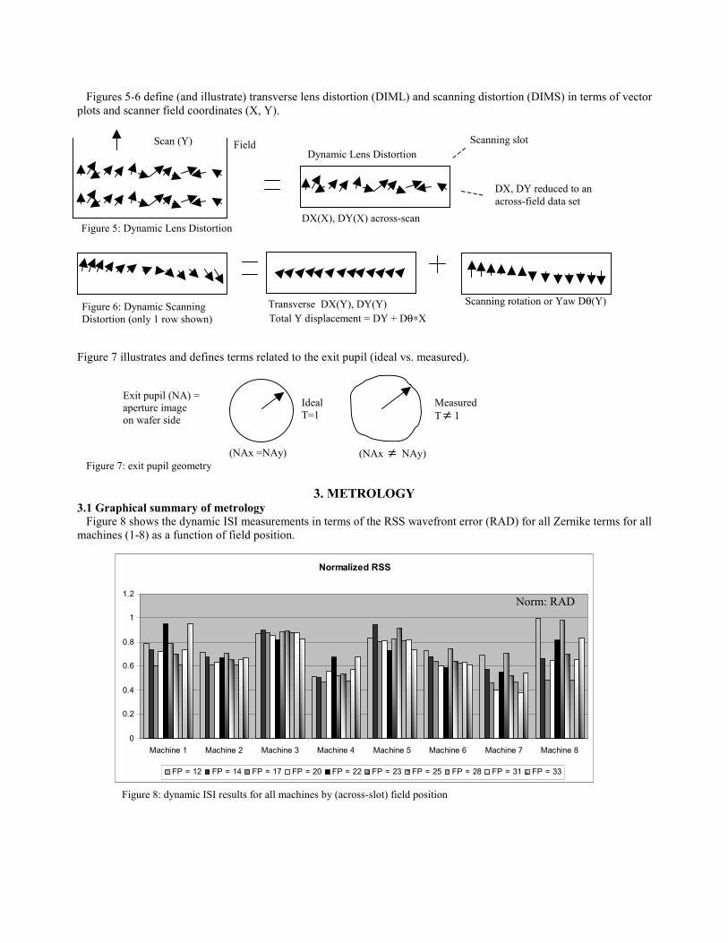
3. METROLOGY 3.1 Graphical summary of metrology Figure 8 shows the dynamic ISI measurements in terms of the RSS wavefront error (RAD) for all Zernike terms for all machines (1-8) as a function of field position. Figure 8: dynamic ISI results for all machines by (across-slot) field position
Normalized RSS
0
0.2
0.4
0.6
0.8
1
1.2
Machine 1 Machine 2 Machine 3 Machine 4 Machine 5 Machine 6 Machine 7 Machine 8
FP = 12 FP = 14 FP = 17 FP = 20 FP = 22 FP = 23 FP = 25 FP = 28 FP = 31 FP = 33
(NAx =NAy)
Exit pupil (NA) = aperture image on wafer side
Ideal T=1
Measured T ≠ 1
(NAx ≠ NAy)
Total Y displacement = DY + Dθ∗X Transverse DX(Y), DY(Y) Scanning rotation or Yaw Dθ(Y)
Figure 6: Dynamic Scanning Distortion (only 1 row shown)
Figure 5: Dynamic Lens Distortion
Scanning slot
DX(X), DY(X) across-scan
Scan (Y)
DX, DY reduced to an across-field data set
Dynamic Lens Distortion Field
Norm: RAD

Statistics (nm)
Following the ISI measurements we use the DIML metrology tool to determine the static and dynamic lens distortion – corrected for high-order aberration feature-shift effects. The results shown below (Tables 1-2) represent normalized data collected/calculated from 32 DIML runs (8 machines, 1 wafer per scanner x 4 DIML patterns/wafer). Table 1 summarizes the dynamic results using the terms defined in Figures 5-6 above. A typical dynamic lens distortion plot for a scanner (at 11 field points) is shown in Figure 9 below (conversion from Figure 9 into Zernikes a2 and a3 follows from λ/π∗ΝΑ). Ηere, lens distortion (nm) is calculated by taking the (DX, DY) average of the standard deviations of the transverse error (or, 1/2(σx+ σy)) – where the standard deviation is derived from 4 DIML scans. Table 1: Dynamic Lens Distortion (nm) Table 2: Static Lens Distortion (nm) Figure 9: example of an across-field Dynamic Lens Distortion Map (typical machine) Repeatability (nm) for the DIML metrology tool was calculated by looking at scan-to-scan differences in DIML performance for each wafer (containing 4 DIML patterns) – since each wafer is scanned with the same lens we expect the same results. The DX, DY (wafer-to-wafer) RMS repeatability (nm) for individual machines ranged from 0.1 to 1.4 nm – and is derived by calculating the (average) standard deviation for each set of transverse errors (163 overlay targets x 2 directions DX, DY x 4 patterns/wafer). The 1-sigma DIML repeatability for all machines taken together is 0.42nm - see Figure 10 (static results were similar). The bin used in the histogram in Figure 10 represents the statistical summary for: 8 machines x 1 wafer/machine x 4 DIML scans/wafer x 163 box-in-box measurements/scan x 2 transverse directions. On average, the statically measured low-order distortion measurements are worse as compared with their scan average (as expected) – these results are summarized in Figure 11.
Figure 10: DIML 1 sigma (nm) repeatability histogram 8 machines

Y=14.7mm
Y = 4.9mm
Y = 2.45mm
Y = 0.0mm
Y = 2.45mm
Y = -4.9mmY = -7.35mm
Y = -9.8mm
Y = -12.25mm
Y = -14.7mm
Y = 12.25mm
Y = 9.8mm
Y = 7.35mm
Vector Scale: 10.0nm
Figure 11: normalized comparison of static and dynamic lens distortion results A typical full-field dynamic scanning distortion plot (for a single scan) is shown in Figure 12 – again, see Figures 5-6 for vector definitions. Table 3 (normalized) lists machine specific scanning distortion - here, scanning distortion (nm) is expressed as the average of 13 pairs (1 pair per scan) of transverse (DX, DY*) standard deviations. Note: as defined earlier, DY* represents the sum of DY + Dθ∗X. Table 4 shows the (normalized) scan-to-scan repeatability for each machine. Repeatability is expressed by taking the average RMS (DX, DY) of the standard deviations that represent transverse scanning error variability by field point (or, ½(RMS(σx) + RMS(σy)). So, in general, the dynamic scan is broken into both a transverse scanning error as well as a rotational component. The appendix shows some interesting ways to plot the transverse error (ternary plots) to help identify the weakest scanner component (lens, stage, feedback system). N.B. we see that the entire group of scanners exhibit a lack modality – e.g., scanners with low distortion might have poor scan repeatability.
Table 3: distortion (nm) Table 4: repeatability (nm) Figure 12: instance of dynamic scanning distortion (typical machine)
The source for each machine was characterized with a high accuracy SMI metrology tool at 25 field points (distributed across the entire field). Figures 13-14 show typical source maps (2 field pts.) for 2 of the 8 scanners used in this study. In general, we found interesting across-field differences – independent of source obscuration. For example, across-field HA-SMI 90% NA energy plots show that machine #6 varies by >2%. Similar machine-to-machine analysis shows ~3% difference (on average) between machines #5 and #2. Lithographic impact for all machines is reported in summary tables below.
The repeatable portion of the scanning error (broken into modes) should be correctable
Figures 13-14: HA-SMI across-field source maps Note the interesting across-field source variation

The last metrology tool investigated is the TMAP (exit pupil mapper) which is used to determine the actual shape of the numerical aperture as a function of field position. Figure 15 shows the max difference in NA for 25 field points by machine number (simulations show that an NA differences of +/-.01 produce 1-2nm ∆CD). Figure 15: max across-field exit pupil (NA) difference by machine
4. SIMULATION & RESULTS 4.1 Simulation description Following metrology, we designed and ran a simulation matrix of experiments (Table 5) to investigate scanner performance as a function of metrology and provide answers to many of our questions and concerns. The following lithographic metrics were used for the gauge study: orientation dependent CD (H-V), feature-shift (XC, YC), and ∆CD for both 200nm and 1000nm trench structures (made from a composite mask with 400nm lines separating the trenches). We use the term ideal (0) to represent the ideal case (perfect component).
Table 5: Note: I=ISI, D=DIML, H=HA-SMI, T=TMAP (8 machines x 2 features x 2 orientations x 51 field pts. x 6 metrology metrics) The ACE simulation process parameters (conditions) are as listed in Table 6 below. The parametric source defined for this experiment is a bit different than those typically discussed in the simulation community. First, due to lack of source metrology data most lithographers use rather simple parametric representations of the source (aberration data is also lacking, but improving since the first introduction of the ISI15). The (modeled or interpolated) parametric sources used in this experiment were derived from the HA-SMI source metrology tool and are not equal to the scanner tool setting (commonly used for parametric source modeling). Reference 16 (see figure 4) shows a rather nice plot of an ideal source and it’s theoretically modeled shape which represents an improvement to simple parametric modeling but falls short of an exact (field pt. by field pt.) representation of the source that can be obtained from HA-SMI analysis. The importance and problems associated with top-hat type parametric source modeling in regards to OPC design are discussed in reference 17 for example. We continue along this path for an important reason, namely, to point-out subtle lithographic effects (feature-shift, H-V bias, and ∆CD) that manifest when simulations include both ISI and HA-SMI metrology data – as noted before2 - especially for ASLV and H-V bias. Since for our work here we collected ISI, HA-SMI, DIML, DIMS, and NA data for 8 scanners at multiple field points we are in a good position to simulate (highlight) these effects and derive some additional statistics.
Abbreviation Lens Distortion Lens Aberration Source Exit Pupil Photoresist Resist ThicknessIdeal (0) Ideal (0) Annular Ellipse Ideal high contrast 500Ideal (0) Ideal (0) HA-SMI Ideal high contrast 500
D, I DMAP ISI Ideal Ideal high contrast 500D, I, H DMAP ISI HA-SMI Ideal high contrast 500
D, I, T DMAP ISI Ideal TMAP high contrast 500D, I , H, T DMAP ISI HA-SMI TMAP high contrast 500
"Max NA - Min NA" by Machines
0.000
0.010
0.020
0.030
0.040
0.050
Machine1
Machine2
Machine3
Machine4
Machine5
Machine6
Machine7
Machine8

51 across-field simulations / machine Machine type scanner Nominal NA <0.75 Nominal sigma 0.7 + obscuration Resist thk./type 500nm: high contrast Feature size small 200nm H&V space Feature size large 1000nm H&V space X, Y, Z MSD / Flare default* Lens Aberrations ISI file* & Source & BW HA-SMI file* Lens distortion DIML file* Scanning distortion DIMS file* Exit pupil TMAP file* Pitch / bars 2000nm / 400nm Table 6: simulation parameters * (dynamic simulation), & (adjusted for focus/wafer height) 4.2 Simulation matrix results (source) The simulation matrix described in Table 5 (rows 1-2) was used to investigate the effect of source non-uniformity on across-field H-V bias for 8 scanner machines. We illustrate results for machine #3 in Figure 16 where we plot across-field H-V bias for 200nm features for both the parametric representation of the source and the high accuracy source metrology tool (HA-SMI). The statistics for the entire H-V bias simulation (2 orientations, 51 across-field points, and 8 machines) is shown in Table 7. We note a rather significant (numerical and statistical) difference between the best-fit parametric source and the HA-SMI H-V bias results. Since the parametric source models (1 for each field pt.) are uniform in intensity but deviated in shape (eccentricity) and centering (CoM) - pt. by pt. across the field – we expect a source balancing problem similar to the physics of poles discussed in reference 18 – and impact to H-V bias. However, since the HA-SMI metrology tool maps-out the complete source intensity function (energy-ellipticity and sigma shape function) field pt. by field pt. we expect even more variation in the HA-SMI simulation results. As expected, it turns out that each scanner does in fact have a unique, across-field H-V bias finger print (actually, this is true for both the parametric and HA-SMI representations) derived from field dependent illumination sources – independent of field dependent aberrations (say coma) and telecentricity. Additionally, we carry the experiment a bit further in regards to aberration-source coupling by looking at across-field feature-shift as a function of source description - Table 8 below (with ideal NA) for all 8 machines.
Table 8: simulation shift-test for best-fit parametric source vs. HA-SMI
Lens Distortion Lens Aberrations Source Exit Pupil PhotoresistIdeal (0) Ideal (0) HA-SMI Ideal high contrastIdeal (0) Ideal (0) Annular Ellipse ideal high contrast
DIML ISI HA-SMI ideal high contrastDIML ISI Annular Ellipse ideal high contrast
CD1 = 200nm (V-space)
CD2 = 1000nm (space)
XC = position
Figure 16: across-field H-V bias (nm)
Table 7: H-V bias difference (HA-SMI vs. Parametric source)

Simulated results for the experimental matrix described in Table 8 are summarized for machine #6 in Figure 17. Without aberrations, the average simulated feature-shift (XC, YC) for parametric source modeling (51 field points = 51 parametric source pts. – some interpolated) was <0.2nm while the average feature-shift for HA-SMI metrology was ~1nm. These results were expected since source geometry for machine #6 was fairly symmetric (sigma) and exhibited only small CoM (energy) shifts (bore-sight error) point-by-point across the field (however small, the HA-SMI data does show a unique across-field pattern while the parametric data was nearly constant). We note more generally (for all machines) that when aberration sets are included along with source simulations (both parametric and HA-SMI) the feature-shifts were on average much larger and a strong function of field position (see Figure 17) – ∆CD yields similar results. Since each scanner is unique in terms of aberrations and source maps we can expect differing results – especially for across-field studies. For this work, we will not go into a theoretical discussion linking source maps with Zernike expansions (pt. by pt. across the field) to derive a coupling function for 200nm feature patterns (although modifying overlay sensitivity equations8 might provide a start to the problem) – rather we choose to summarize results. However, since we have access to the ACE emulation engine we are in a good position to model any desired interaction simply by changing dynamic emulation conditions using actual metrology data19 and other critical lithographic variables (feature size, pitch, focus, and telecentricity). Figure 17: feature-shift (nm) comparison for HA-SMI and parametric source (with ISI & DIML) 4.3 Simulation matrix results (metrology) We summarize the important results from the simulation matrix experiment (see Table 5 above) where we investigate the lithographic impact (feature-shift and ∆CD) as a function of scanner metrology. Figure 18 shows a simulation summary (frequency histogram) for feature-shift simulations (for 2 features, 2 orientations, 51 across-field points, and 8 machines) when simulations included the entire suite of metrology tools (ISI+DIML+HA-SMI+TMAP) as well as partial sets (ISI + DIML) and (ISI + DIML + HA-SMI). As can be seen, the ISI + DIML simulations accounted for most of the feature-shift (R2 ~ 0.96) – including HA-SMI metrology just about accounted for the rest of the feature-shift (R2 > 0.99). Additional learning is summarized in the conclusion section.
Machine 6Small Shift Comparison: Ideal vs. HA-SMI Sources with Aberration
-8.00
-6.00
-4.00
-2.00
0.00
2.00
4.00
6.00
-13 -12 -11 -10 -9 -8 -7 -6 -5 -4 -3 -2 -1 0 1 2 3 4 5 6 7 8 9 10 11 12 13
Ideal Source with Aberrations, XC HA-SMI Source with Aberrations, XC
Figure 18: RMS shift and feature-shift differences as a function of metrology used during simulation

Figure 19 shows the ∆CD simulation results (frequency histogram) for 2 features, 2 orientations (H-V), 51 across-field points, and 8 machines - where (again) we compare simulated results for different sets of scanner metrology. As can be seen, field dependent CD variation (∆CD) requires accurate ISI, DIML, HA-SMI, and TMAP data for full explanation. 4.4 Simulation matrix results (lithography) Figure 20 shows across-field ∆CD (delta CD from machine average) simulation results for the best and worse case machine pair using the complete suite of metrology tools. Tables 9-11 summarize the maximum lithographic effects which could be used to identify problematic machines (where here: max ∆CD = difference between the smallest and largest across-field CD, max |HV| = max across-field H-V bias, max |shift| = max across-field feature-shift).
Table 9: max ∆CD (nm)
Table 10: max H-V (nm)
Figure 19: RMS ∆CD (nm) as a function of metrology used during simulation
Small Feature---Cross Field CD Variation (nm)
-6.00
-4.00
-2.00
0.00
2.00
4.00
6.00
8.00
10.00
12.00
14.00
-13 -11 -9 -7 -5 -3 -1 1 3 5 7 9 11 13
Machine 3, CDX Machine 3, CDY Machine 6, CDX Machine 6, CDY
Figure 20: ∆CD (nm) results good/bad machine 2 feature directions
Table 11: max feature-shift (nm)

5. CONCLUSIONS 5.1 Précis We summarize our critical learning from this rather massive metrology and simulation study in Tables 12-13 below. For our metrology experiments, we summarize machine-to-machine differences, metrology tool repeatability, and some general comments. For our simulation results, we focus on H-V bias, feature-shift, and ∆CD for both machine-to-machine (#1-#8) differences and across-field behavior. Metrology tool max machine deltas metrology tool repeatability general comments
In-Situ interferometer dynamic (ISI)
#3 - #4 = ~50% RSS wave error delta
< 0.1nm taken from 2 rows, 5 field pts.
spherical terms corrected for focus
Lens distortion (DIML)
#7 - #6 = .36nm normalized
static = 1.42nm dynamic = 0.42nm
accurate a2 & a3 = better matching
Scan distortion (DIMS)19
#8 - #4 = .33nm normalized
R2 ~0.9 DIMS accounts for error
stage yaw, #6 >0.02 µRAD*
Scan repeatability (DIMS)
# 7 - #8 = 0.07 nm normalized
R2 ~0.9 DIMS accounts for error
#6 & #7 poor scan repeatability
Source metrology (HA-SMI)
#5 - #2 ~3% delta for NA90% energy radius
10x resolution vs. SMI
Exit pupil (TMAP) #8 - #2 >.01** (NA) ~.002 (1-sigma) CD impact Table 12: metrology summary (*normalized from collected data, **average difference) Simulation (200nm) max machine delta max across-field required metrology input
H-V #3-#6 = 2.12nm #1 = 4.23nm I, H Feature-shift #3-#5 =10.62nm #3 = 18.93nm I, D, DIMS19 ∆CD #3-#6 =12.5nm #3 = 15.85nm I, D, T
Table 13: simulation summary using all metrology tools 5.2 Applications and developments Earlier we touched on several potential applications related to our metrology investigation and simulated results. We focus now on describing some additional ideas related to both parts of our study. Table 14 shows a list of potential fab- oriented applications. For fabs, the group behavior of tools sets is probably most important (machine routing for example) as opposed to smaller research fabs that are more generally interested in one critical set of data (1 good aberration set). The following ternary diagram (Figure 21) offers an additional suggestion or application: here we plot dynamic lens distortion, scanning distortion, and scanner repeatability (variance) for self-normalized machines (sum of squares set to 1). We note here that while machine #8 has good scan repeatability (both self-referenced and as given in Table 4) its fractional amount of scanning distortion is rather high. In fact, further investigation (see Table 3) shows machine #8 had the worse overall scanning distortion as well – this implies a systematic (dynamic) problem that might be correctable.
Figure 21: DIML, DIMS, and scan repeatability
Ternary Plot
0.2
0.4
0.6
0.8
1 0
0.2
0.4
0.6
0.8
00.20.40.60.8
Scan Repeat ̂ 2 (avg. sigma nm)
# 6
# 8

Application Comment (impact) overlay control and machine matching route is process and mask dependent (yield improvement) transverse overlay analysis see ternary diagram for example (CoO improvement) mask design (using emulation) improve mask design (robust: less defect sensitive) scanner control stage amelioration (CoO improvement) process control and monitoring weekly metrology and simulation (yield improvement) lithographic analysis (yield, DoF vs. EL, PW etc.,) complete lithographic analysis (process improvement) Table 14: potential applications for the simulation performance framework Monitoring the performance of projection imaging tools using a suite of accurate and repeatable in-situ metrology tools whose outputs are automatically integrated into a (time-sensitive) lithographic framework should give semiconductor manufacturers and sagacious simulators an edge on developing new products by providing the a framework for Predictive LithographyTM.
ACKNOWLEDGEMENTS The authors would like to thank the Intel Rio-Rancho F11 facility for providing fab access. Special thanks to Bernie Wilimitis and F11 Laser Manufacturing for approving tool-time and supporting this work. Finally, thanks again to Litel Instruments for providing Dynamic Intelligence Inc. the opportunity to have access to the ACE simulation framework.
REFERENCES 1. PROLITHTM (KLA-Tencor), Solid-CTM (Sigma-C) 2. G. Zhang, et al., “Illumination Pupil Fill Measurement and Analysis and Its Application in Scanner V-H Bias Characterization for 130nm Node and Beyond,” Optical Microlithography XVI, Proc., SPIE vol. 5040-5, p. 45-56, 2003. 3. P. De Bisschop, “Evaluation of Litel’s In-Situ Interferometer (ISI) technique for measuring Projection Lens aberrations: an initial study,” Optical Microlithography XVI, Proc., SPIE vol. 5040-2, p. 11-23, 2003. 4. S. Slonaker, et al., “Application of in-situ aberration measurements to pattern-specific imaging optimization,” Optical Microlithography XVI, Proc., SPIE vol. 5040-33, p. 371-382, 2003. 5. High Accuracy Source Metrology Instrument (HA-SMI)TM and Analysis Characterization Engine (ACE)TM (Litel Instruments) 6 B. Streefkerk, et al., “Extending optical lithography with immersion,” Optical Microlithography XVII, Proc., SPIE vol. 5377-25, p. 285-305, 2004. 7. C. Progler, et al., “Impact of lithography variability on statistical timing behavior,” Design and Process Integration for Microelectronic Manufacturing II, Proc., SPIE vol. 5379-14, p. 101-110, 2004. 8. P. Gräupner, et al., “Impact of wavefront errors on low k1 processes at extreme high NA,” Optical Microlithography XVI, Proc., SPIE vol. 5040-12, p. 119-130, 2003. 9. J. Petersen, “Optical proximity strategies for desensitizing lens aberrations,” Lithography for Semiconductor Manufacturing II, SPIE vol. 4404-33, p. 1-13, 2001. 10. D. Flagello, et al., “Optimizing and Enhancing Optical Systems to Meet the Low k1 Challenge,” Optical Microlithography XVI, Proc., SPIE vol. 5040-14, p. 139-150, 2003. 11. B. Smith, “Mutually Optimizing Resolution Enhancement Techniques: Illumination, APSM, Assist Feature OPC, and Gray Bars,” Optical Microlithography, Proc., SPIE vol. 4348-48, (15 pages), 2001. 12. G. Zhang, et al., “Illumination Pupil Fill Measurement and Analysis and Its Application in Scanner V-H Bias Characterization for 130nm Node and Beyond,” Optical Microlithography XVI, Proc., SPIE vol. 5040-5, p. 45-56, 2003. 13. J. Armitage, “Analysis of Overlay Distortion Patterns,” Integrated Circuit Metrology, Inspection and Process Control II Proc., SPIE 921 (1988). 14. S. Renwick, et al., “Influence of laser spatial parameters and illuminator pupil-fill on lithographic performance of a scanner,” Optical Microlithography, Proc., SPIE vol. 4691-195, p. 1400-1411, 2002. 15. N. Farrar, et al., “In-situ measurement of lens aberrations,” Optical Microlithography XIII, Proc., SPIE vol. 4000, p. 18-29, 2000. 16. C. Hwang, et al., “Impact of illumination intensity profile on lithography simulation,” Optical Microlithography XVII, Proc., SPIE vol. 5377-149, p. 1427-1434, 2004. 17. C. Bodendorf, et al., “Impact of Measured Pupil Illumination Fill Distribution on Lithography Simulation and OPC models,” Optical Microlithography XVII, Proc., SPIE vol. 5377-110, p. 1130-1145, 2004. 18. J. Sheats, B. Smith, Microlithography: science and technology, Marcel Dekker; ISBN: 0824799534, New York, NY, 1998. 19. A. Smith, U.S. Patent forth coming, “Method and Apparatus for Self-Referenced Dynamic Step and Scan Intra-Field Scanning Distortion.”