ad73322l low cost, low power cmos general-purpose dual
TRANSCRIPT

Low Cost, Low Power CMOSGeneral-Purpose Dual Analog Front End
AD73322L
Rev. A Information furnished by Analog Devices is believed to be accurate and reliable. However, no responsibility is assumed by Analog Devices for its use, nor for any infringements of patents or other rights of third parties that may result from its use. Specifications subject to change without notice. No license is granted by implication or otherwise under any patent or patent rights of Analog Devices. Trademarks and registered trademarks are the property of their respective owners.
One Technology Way, P.O. Box 9106, Norwood, MA 02062-9106, U.S.A. Tel: 781.329.4700 www.analog.com Fax: 781.326.8703 © 2004 Analog Devices, Inc. All rights reserved.
FEATURES Two 16-bit A/D converters Two 16-bit D/A converters Programmable input/output sample rates 78 dB ADC SNR 78 dB DAC SNR 64 kHz maximum sample rate −90 dB crosstalk Low group delay (25 µs typ per ADC channel, 50 µs typ per
DAC channel) Programmable input/output gain Flexible serial port allows up to 4 dual codecs to be
connected in cascade, giving 8 I/O channels Single-supply operation (2.7 V to 3.3 V) 50 mW typ power consumption at 3.0 V Temperature range: −40°C to +105°C On-chip reference 28-lead SOIC, TSSOP, and 44-lead LQFP packages
APPLICATIONS General-purpose analog I/O Speech processing Cordless and personal communications Telephony Active control of sound and vibration Data communications Wireless local loop
GENERAL DESCRIPTION
The AD73322L is a dual front-end processor for general-purpose applications, including speech and telephony. It features two 16-bit A/D conversion channels and two 16-bit D/A conversion channels. Each channel provides 78 dB signal-to-noise ratio over a voice-band signal bandwidth. It also features an input-to-output gain network in both the analog and digital domains. This is featured on both codecs and can be used for impedance matching or scaling when interfacing to subscriber line interface circuits (SLICs).
The AD73322L is particularly suitable for a variety of appli-cations in the speech and telephony area, including low bit rate, high quality compression, speech enhancement, recognition, and synthesis. The low group delay characteristic of the part makes it suitable for single or multichannel active control applications.
FUNCTIONAL BLOCK DIAGRAM
SDOFS
ADC CHANNEL 1
REFERENCE
DAC CHANNEL 1
ADC CHANNEL 2
DAC CHANNEL 2
SPORT
AVDD1 AVDD2 DVDD
VFBP1VINP1VINN1
VFBN1
VFBP2VINP2VINN2
VFBN2
VOUTP2VOUTN2
AGND1 AGND2 DGND
SDO
MCLK
RESETSE
SCLK
SDIFSSDI
AD73322L
0069
1-00
1
VOUTP1VOUTN1
REFCAPREFOUT
Figure 1.
The A/D and D/A conversion channels feature programmable input/output gains with ranges of 38 dB and 21 dB, respectively. An on-chip reference voltage allows single-supply operation.
The sampling rate of the codecs is programmable with four separate settings offering 64 kHz, 32 kHz, 16 kHz, and 8 kHz sampling rates (from a master clock of 16.384 MHz).
A serial port (SPORT) allows easy interfacing of single or cascaded devices to industry-standard DSP engines. The SPORT transfer rate is programmable to allow interfacing to both fast and slow DSP engines.
The AD73322L is available in 28-lead SOIC, 28-lead TSSOP, and 44-lead LQFP packages.
AD73322L
Rev. A | Page 2 of 48
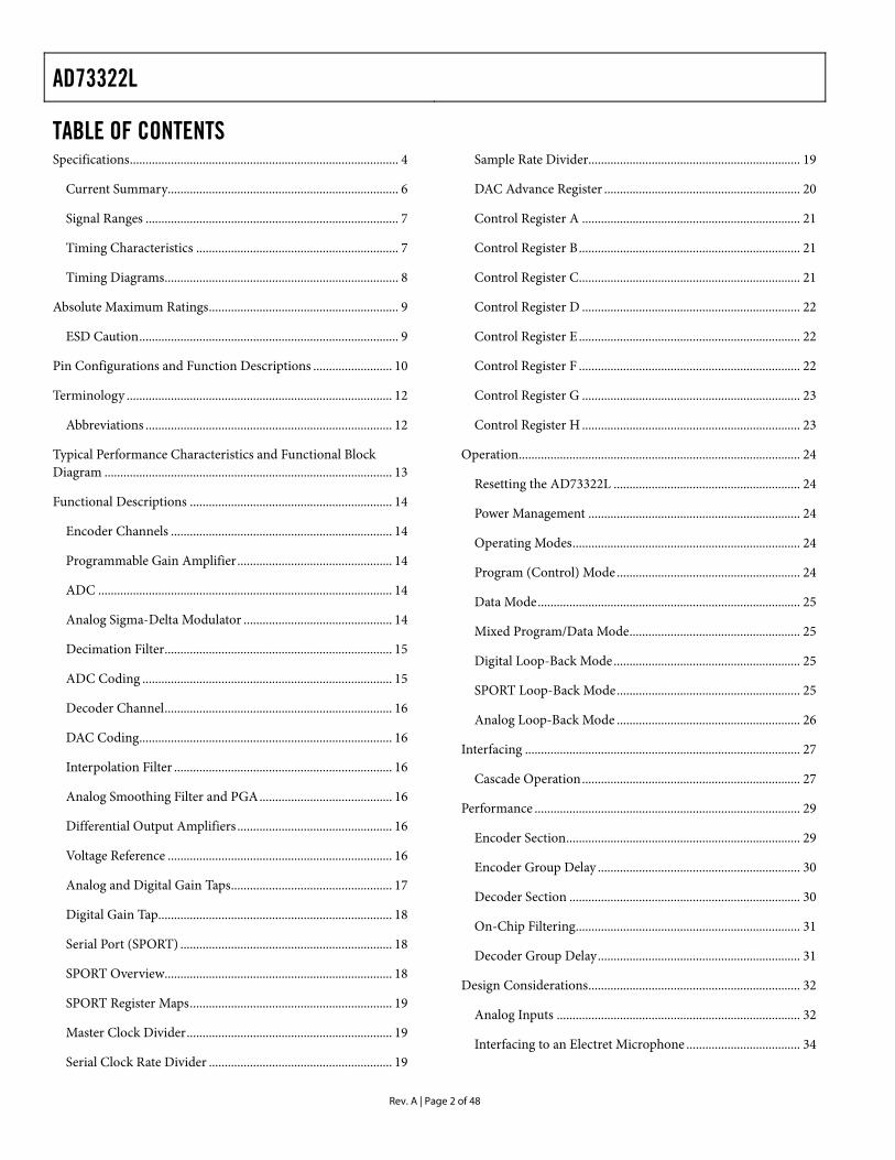
TABLE OF CONTENTS Specifications..................................................................................... 4
Current Summary......................................................................... 6
Signal Ranges ................................................................................ 7
Timing Characteristics ................................................................ 7
Timing Diagrams.......................................................................... 8
Absolute Maximum Ratings............................................................ 9
ESD Caution.................................................................................. 9
Pin Configurations and Function Descriptions ......................... 10
Terminology .................................................................................... 12
Abbreviations .............................................................................. 12
Typical Performance Characteristics and Functional Block Diagram ........................................................................................... 13
Functional Descriptions ................................................................ 14
Encoder Channels ...................................................................... 14
Programmable Gain Amplifier................................................. 14
ADC ............................................................................................. 14
Analog Sigma-Delta Modulator ............................................... 14
Decimation Filter........................................................................ 15
ADC Coding ............................................................................... 15
Decoder Channel........................................................................ 16
DAC Coding................................................................................ 16
Interpolation Filter ..................................................................... 16
Analog Smoothing Filter and PGA.......................................... 16
Differential Output Amplifiers ................................................. 16
Voltage Reference ....................................................................... 16
Analog and Digital Gain Taps................................................... 17
Digital Gain Tap.......................................................................... 18
Serial Port (SPORT) ................................................................... 18
SPORT Overview........................................................................ 18
SPORT Register Maps................................................................ 19
Master Clock Divider................................................................. 19
Serial Clock Rate Divider .......................................................... 19
Sample Rate Divider................................................................... 19
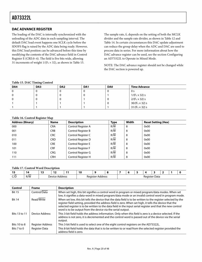
DAC Advance Register .............................................................. 20
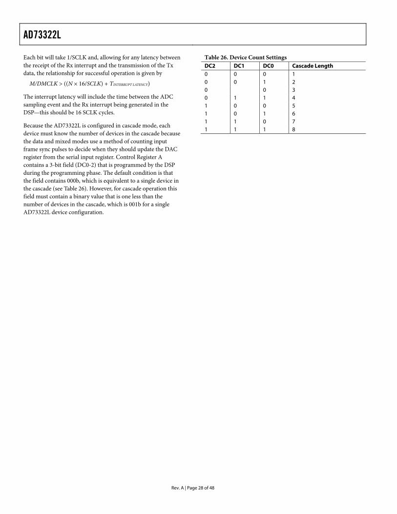
Control Register A ..................................................................... 21
Control Register B...................................................................... 21
Control Register C...................................................................... 21
Control Register D ..................................................................... 22
Control Register E ...................................................................... 22
Control Register F ...................................................................... 22
Control Register G ..................................................................... 23
Control Register H ..................................................................... 23
Operation......................................................................................... 24
Resetting the AD73322L ........................................................... 24
Power Management ................................................................... 24
Operating Modes........................................................................ 24
Program (Control) Mode .......................................................... 24
Data Mode................................................................................... 25
Mixed Program/Data Mode...................................................... 25
Digital Loop-Back Mode........................................................... 25
SPORT Loop-Back Mode.......................................................... 25
Analog Loop-Back Mode .......................................................... 26
Interfacing ....................................................................................... 27
Cascade Operation..................................................................... 27
Performance .................................................................................... 29
Encoder Section.......................................................................... 29
Encoder Group Delay ................................................................ 30
Decoder Section ......................................................................... 30
On-Chip Filtering....................................................................... 31
Decoder Group Delay................................................................ 31
Design Considerations................................................................... 32
Analog Inputs ............................................................................. 32
Interfacing to an Electret Microphone .................................... 34
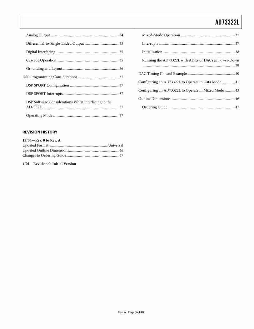
AD73322L
Rev. A | Page 3 of 48
Analog Output.............................................................................34
Differential-to-Single-Ended Output .......................................35
Digital Interfacing .......................................................................35
Cascade Operation......................................................................35
Grounding and Layout ...............................................................36
DSP Programming Considerations ..............................................37
DSP SPORT Configuration .......................................................37
DSP SPORT Interrupts...............................................................37
DSP Software Considerations When Interfacing to the AD73322L ....................................................................................37
Operating Mode ..........................................................................37
Mixed-Mode Operation.............................................................37
Interrupts .....................................................................................37
Initialization.................................................................................38
Running the AD73322L with ADCs or DACs in Power-Down.......................................................................................................38
DAC Timing Control Example .....................................................40
Configuring an AD73322L to Operate in Data Mode ...............41
Configuring an AD73322L to Operate in Mixed Mode ............43
Outline Dimensions........................................................................46
Ordering Guide ...........................................................................47
REVISION HISTORY
12/04—Rev. 0 to Rev. A Updated Format.................................................................. Universal Updated Outline Dimensions........................................................46 Changes to Ordering Guide...........................................................47
4/01—Revision 0: Initial Version
AD73322L
Rev. A | Page 4 of 48
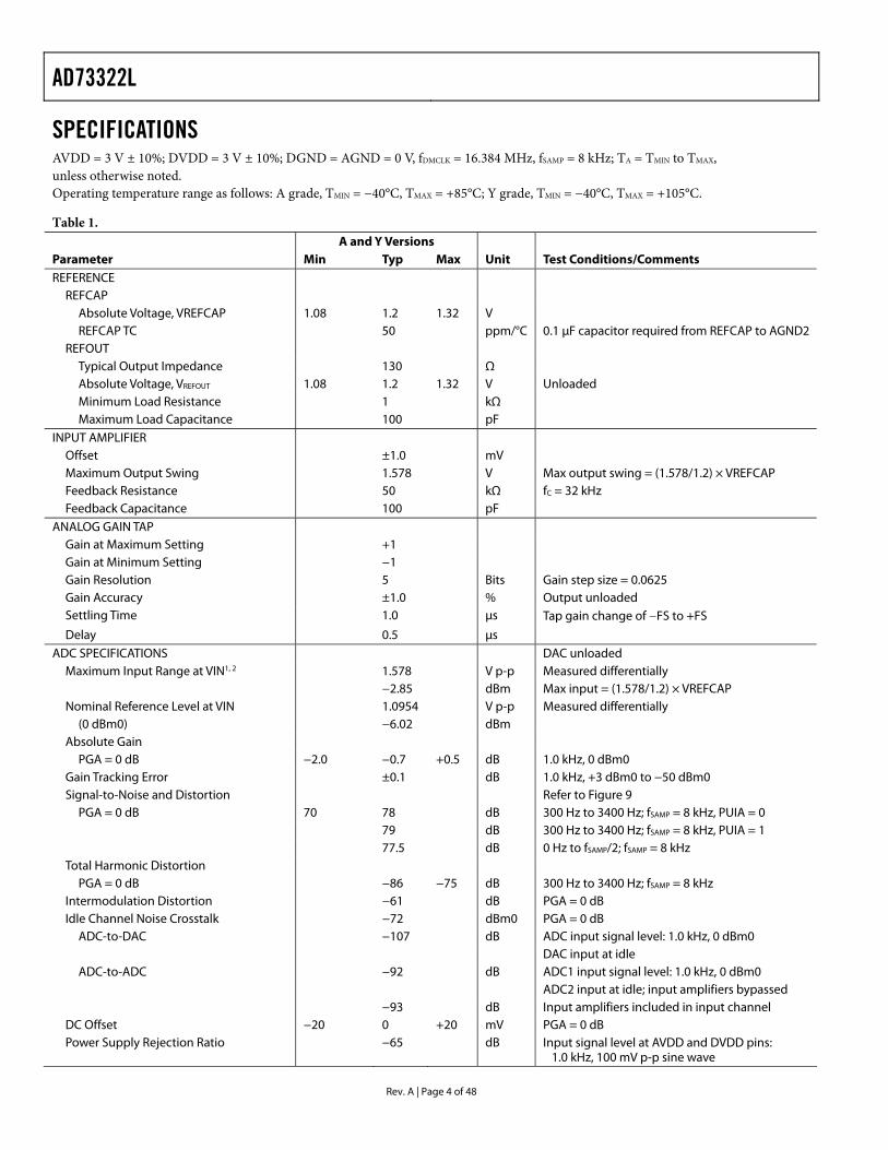
SPECIFICATIONS AVDD = 3 V ± 10%; DVDD = 3 V ± 10%; DGND = AGND = 0 V, fDMCLK = 16.384 MHz, fSAMP = 8 kHz; TA = TMIN to TMAX, unless otherwise noted. Operating temperature range as follows: A grade, TMIN = −40°C, TMAX = +85°C; Y grade, TMIN = −40°C, TMAX = +105°C.
Table 1. A and Y Versions Parameter Min Typ Max Unit Test Conditions/Comments REFERENCE
REFCAP Absolute Voltage, VREFCAP 1.08 1.2 1.32 V REFCAP TC 50 ppm/°C 0.1 µF capacitor required from REFCAP to AGND2
REFOUT Typical Output Impedance 130 Ω Absolute Voltage, VREFOUT 1.08 1.2 1.32 V Unloaded Minimum Load Resistance 1 kΩ Maximum Load Capacitance 100 pF
INPUT AMPLIFIER Offset ±1.0 mV Maximum Output Swing 1.578 V Max output swing = (1.578/1.2) × VREFCAP Feedback Resistance 50 kΩ fC = 32 kHz Feedback Capacitance 100 pF
ANALOG GAIN TAP Gain at Maximum Setting +1 Gain at Minimum Setting −1 Gain Resolution 5 Bits Gain step size = 0.0625 Gain Accuracy ±1.0 % Output unloaded Settling Time 1.0 µs Tap gain change of −FS to +FS
Delay 0.5 µs ADC SPECIFICATIONS DAC unloaded
Maximum Input Range at VIN1, 2 1.578 V p-p Measured differentially −2.85 dBm Max input = (1.578/1.2) × VREFCAP Nominal Reference Level at VIN 1.0954 V p-p Measured differentially
(0 dBm0) −6.02 dBm Absolute Gain
PGA = 0 dB −2.0 −0.7 +0.5 dB 1.0 kHz, 0 dBm0 Gain Tracking Error ±0.1 dB 1.0 kHz, +3 dBm0 to −50 dBm0 Signal-to-Noise and Distortion Refer to Figure 9
PGA = 0 dB 70 78 dB 300 Hz to 3400 Hz; fSAMP = 8 kHz, PUIA = 0 79 dB 300 Hz to 3400 Hz; fSAMP = 8 kHz, PUIA = 1 77.5 dB 0 Hz to fSAMP/2; fSAMP = 8 kHz Total Harmonic Distortion
PGA = 0 dB −86 −75 dB 300 Hz to 3400 Hz; fSAMP = 8 kHz Intermodulation Distortion −61 dB PGA = 0 dB Idle Channel Noise Crosstalk −72 dBm0 PGA = 0 dB
ADC-to-DAC −107 dB ADC input signal level: 1.0 kHz, 0 dBm0 DAC input at idle
ADC-to-ADC −92 dB ADC1 input signal level: 1.0 kHz, 0 dBm0 ADC2 input at idle; input amplifiers bypassed −93 dB Input amplifiers included in input channel DC Offset −20 0 +20 mV PGA = 0 dB Power Supply Rejection Ratio −65 dB Input signal level at AVDD and DVDD pins:
1.0 kHz, 100 mV p-p sine wave
AD73322L
Rev. A | Page 5 of 48
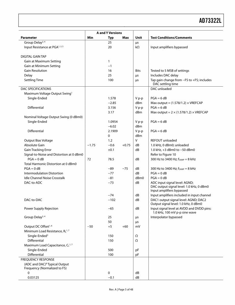
A and Y Versions Parameter Min Typ Max Unit Test Conditions/Comments
Group Delay3, 4 25 µs Input Resistance at PGA1, 3, 5 20 kΩ Input amplifiers bypassed
DIGITAL GAIN TAP Gain at Maximum Setting 1 Gain at Minimum Setting −1 Gain Resolution 16 Bits Tested to 5 MSB of settings Delay 25 µs Includes DAC delay Settling Time 100 µs Tap gain change from −FS to +FS; includes
DAC settling time DAC SPECIFICATIONS DAC unloaded
Maximum Voltage Output Swing1 Single-Ended 1.578 V p-p PGA = 6 dB −2.85 dBm Max output = (1.578/1.2) × VREFCAP Differential 3.156 V p-p PGA = 6 dB
3.17 dBm Max output = 2 × (1.578/1.2) × VREFCAP Nominal Voltage Output Swing (0 dBm0)
Single-Ended 1.0954 V p-p PGA = 6 dB −6.02 dBm Differential 2.1909 V p-p PGA = 6 dB
0 dBm Output Bias Voltage 1.2 V REFOUT unloaded Absolute Gain −1.75 −0.6 +0.75 dB 1.0 kHz, 0 dBm0; unloaded Gain Tracking Error ±0.1 dB 1.0 kHz, +3 dBm0 to −50 dBm0 Signal-to-Noise and Distortion at 0 dBm0 Refer to Figure 10
PGA = 0 dB 72 78.5 dB 300 Hz to 3400 Hz; fSAMP = 8 kHz Total Harmonic Distortion at 0 dBm0 PGA = 0 dB −89 −75 dB 300 Hz to 3400 Hz; fSAMP = 8 kHz Intermodulation Distortion −77 dB PGA = 0 dB Idle Channel Noise Crosstalk −81 dBm0 PGA = 0 dB DAC-to-ADC −73 dB ADC input signal level: AGND;
DAC output signal level: 1.0 kHz, 0 dBm0 Input amplifiers bypassed
−74 dB Input amplifiers included in input channel DAC-to-DAC −102 dB DAC1 output signal level: AGND; DAC2
Output signal level: 1.0 kHz, 0 dBm0 Power Supply Rejection −65 dB Input signal level at AVDD and DVDD pins:
1.0 kHz, 100 mV p-p sine wave Group Delay3, 4 25 µs Interpolator bypassed 50 µs Output DC Offset1, 6 −50 +5 +60 mV Minimum Load Resistance, RL
1, 7 Single-Ended3 150 Ω Differential 150 Ω
Maximum Load Capacitance, CL1, 7
Single-Ended 500 pF Differential 100 pF
FREQUENCY RESPONSE (ADC and DAC)8 Typical Output Frequency (Normalized to FS)
0 0 dB 0.03125 −0.1 dB
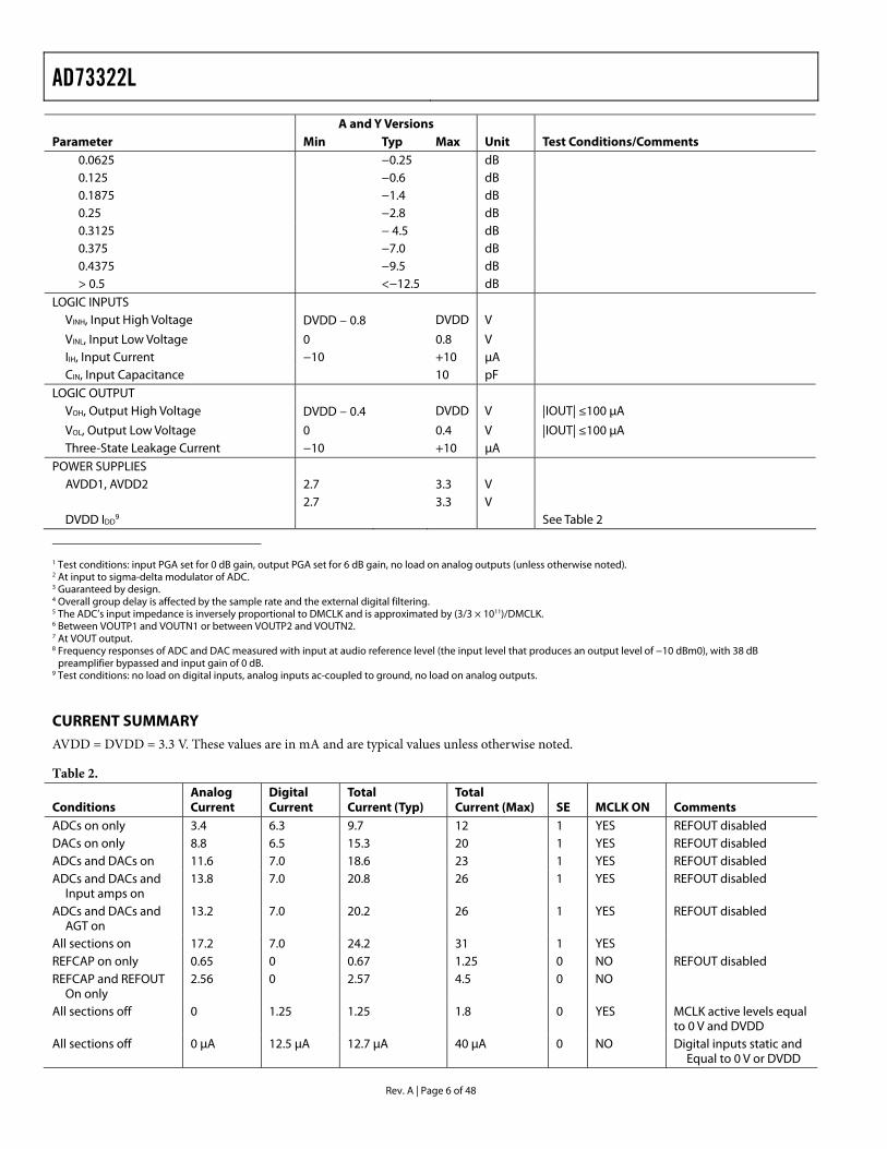
AD73322L
Rev. A | Page 6 of 48
A and Y Versions Parameter Min Typ Max Unit Test Conditions/Comments
0.0625 −0.25 dB 0.125 −0.6 dB 0.1875 −1.4 dB 0.25 −2.8 dB 0.3125 − 4.5 dB 0.375 −7.0 dB 0.4375 −9.5 dB > 0.5 <−12.5 dB
LOGIC INPUTS VINH, Input High Voltage DVDD − 0.8 DVDD V
VINL, Input Low Voltage 0 0.8 V IIH, Input Current −10 +10 µA CIN, Input Capacitance 10 pF
LOGIC OUTPUT VOH, Output High Voltage DVDD − 0.4 DVDD V |IOUT| ≤100 µA
VOL, Output Low Voltage 0 0.4 V |IOUT| ≤100 µA Three-State Leakage Current −10 +10 µA
POWER SUPPLIES AVDD1, AVDD2 2.7 3.3 V 2.7 3.3 V DVDD IDD
9 See Table 2
1 Test conditions: input PGA set for 0 dB gain, output PGA set for 6 dB gain, no load on analog outputs (unless otherwise noted). 2 At input to sigma-delta modulator of ADC. 3 Guaranteed by design. 4 Overall group delay is affected by the sample rate and the external digital filtering. 5 The ADC’s input impedance is inversely proportional to DMCLK and is approximated by (3/3 × 1011)/DMCLK. 6 Between VOUTP1 and VOUTN1 or between VOUTP2 and VOUTN2. 7 At VOUT output. 8 Frequency responses of ADC and DAC measured with input at audio reference level (the input level that produces an output level of −10 dBm0), with 38 dB
preamplifier bypassed and input gain of 0 dB. 9 Test conditions: no load on digital inputs, analog inputs ac-coupled to ground, no load on analog outputs.
CURRENT SUMMARY AVDD = DVDD = 3.3 V. These values are in mA and are typical values unless otherwise noted.
Table 2.
Conditions Analog Current
Digital Current
Total Current (Typ)
Total Current (Max) SE MCLK ON Comments
ADCs on only 3.4 6.3 9.7 12 1 YES REFOUT disabled DACs on only 8.8 6.5 15.3 20 1 YES REFOUT disabled ADCs and DACs on 11.6 7.0 18.6 23 1 YES REFOUT disabled ADCs and DACs and
Input amps on 13.8 7.0 20.8 26 1 YES REFOUT disabled
ADCs and DACs and AGT on
13.2 7.0 20.2 26 1 YES REFOUT disabled
All sections on 17.2 7.0 24.2 31 1 YES REFCAP on only 0.65 0 0.67 1.25 0 NO REFOUT disabled REFCAP and REFOUT
On only 2.56 0 2.57 4.5 0 NO
All sections off 0 1.25 1.25 1.8 0 YES MCLK active levels equal to 0 V and DVDD
All sections off 0 µA 12.5 µA 12.7 µA 40 µA 0 NO Digital inputs static and Equal to 0 V or DVDD
AD73322L
Rev. A | Page 7 of 48
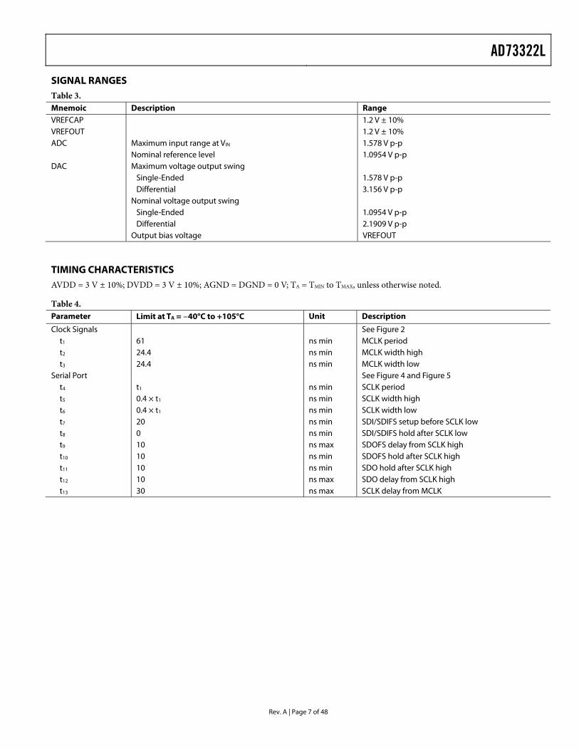
SIGNAL RANGES Table 3. Mnemoic Description Range VREFCAP 1.2 V ± 10% VREFOUT 1.2 V ± 10% ADC Maximum input range at VIN 1.578 V p-p Nominal reference level 1.0954 V p-p DAC Maximum voltage output swing Single-Ended 1.578 V p-p Differential 3.156 V p-p Nominal voltage output swing Single-Ended 1.0954 V p-p Differential 2.1909 V p-p Output bias voltage VREFOUT
TIMING CHARACTERISTICS AVDD = 3 V ± 10%; DVDD = 3 V ± 10%; AGND = DGND = 0 V; TA = TMlN to TMAX, unless otherwise noted.
Table 4. Parameter Limit at TA = −40°C to +105°C Unit Description
Clock Signals See Figure 2 t1 61 ns min MCLK period t2 24.4 ns min MCLK width high t3 24.4 ns min MCLK width low
Serial Port See Figure 4 and Figure 5 t4 t1 ns min SCLK period t5 0.4 × t1 ns min SCLK width high t6 0.4 × t1 ns min SCLK width low t7 20 ns min SDI/SDIFS setup before SCLK low t8 0 ns min SDI/SDIFS hold after SCLK low t9 10 ns max SDOFS delay from SCLK high t10 10 ns min SDOFS hold after SCLK high t11 10 ns min SDO hold after SCLK high t12 10 ns max SDO delay from SCLK high t13 30 ns max SCLK delay from MCLK
AD73322L
Rev. A | Page 8 of 48
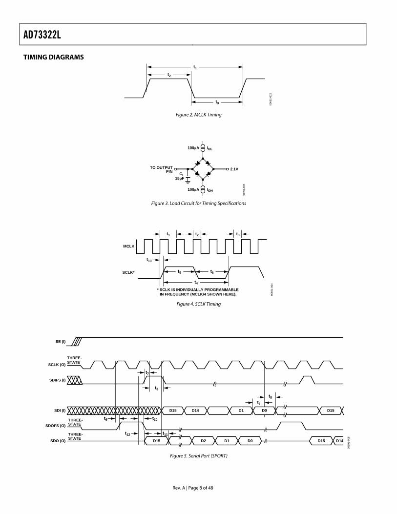
TIMING DIAGRAMS
0069
1-00
2
t1
t2
t3
Figure 2. MCLK Timing
0069
1-00
3
100µA IOL
100µA IOH
2.1VTO OUTPUTPIN CL
15pF
Figure 3. Load Circuit for Timing Specifications
* SCLK IS INDIVIDUALLY PROGRAMMABLEIN FREQUENCY (MCLK/4 SHOWN HERE).
MCLK
SCLK*00
691-
004
t1 t2 t3
t13
t5 t6
t4
Figure 4. SCLK Timing
SE (I)
SCLK (O)
SDIFS (I)
SDI (I)
SDOFS (O)
SDO (O)
THREE-STATE
THREE-STATE
THREE-STATE D15 D2 D1 D0 D14
D15D0D1D14D15
D15
0069
1-00
5
t7
t9
t8
t10
t12 t11
t7
t8
Figure 5. Serial Port (SPORT)
AD73322L
Rev. A | Page 9 of 48
ABSOLUTE MAXIMUM RATINGS TA = 25°C unless otherwise noted.
Table 5. Parameters Ratings AVDD, DVDD to GND −0.3 V to +4.6 V AGND to DGND −0.3 V to +0.3 V Digital I/O Voltage to DGND −0.3 V to (DVDD + 0.3 V) Analog I/O Voltage to AGND −0.3 V to (AVDD + 0.3 V) Operating Temperature Range
Industrial (A Version) −40°C to +85°C Extended (Y Version) −40°C to +105°C
Storage Temperature Range −65°C to +150°C Maximum Junction Temperature 150°C SOIC, θJA Thermal Impedance 71.4°C/W Lead Temperature, Soldering
Vapor Phase (60 sec) 215°C Infrared (15 sec) 220°C
LQFP, θJA Thermal Impedance 53.2°C/W Lead Temperature, Soldering
Vapor Phase (60 sec) 215°C Infrared (15 sec) 220°C
TSSOP, θJA Thermal Impedance 97.9°C/W Lead Temperature, Soldering
Vapor Phase (60 sec) 215°C Infrared (15 sec) 220°C
Stresses above those listed under Absolute Maximum Ratings may cause permanent damage to the device. This is a stress rating only; functional operation of the device at these or any other conditions above those listed in the operational sections of this specification is not implied. Exposure to absolute maximum rating conditions for extended periods may affect device reliability.
ESD CAUTION ESD (electrostatic discharge) sensitive device. Electrostatic charges as high as 4000 V readily accumulate on the uman body and test equipment and can discharge without detection. Although this product features proprietary ESD protection circuitry, permanent damage may occur on devices subjected to high energy electrostatic discharges. Therefore, proper ESD precautions are recommended to avoid performance degradation or loss of functionality.
AD73322L
Rev. A | Page 10 of 48
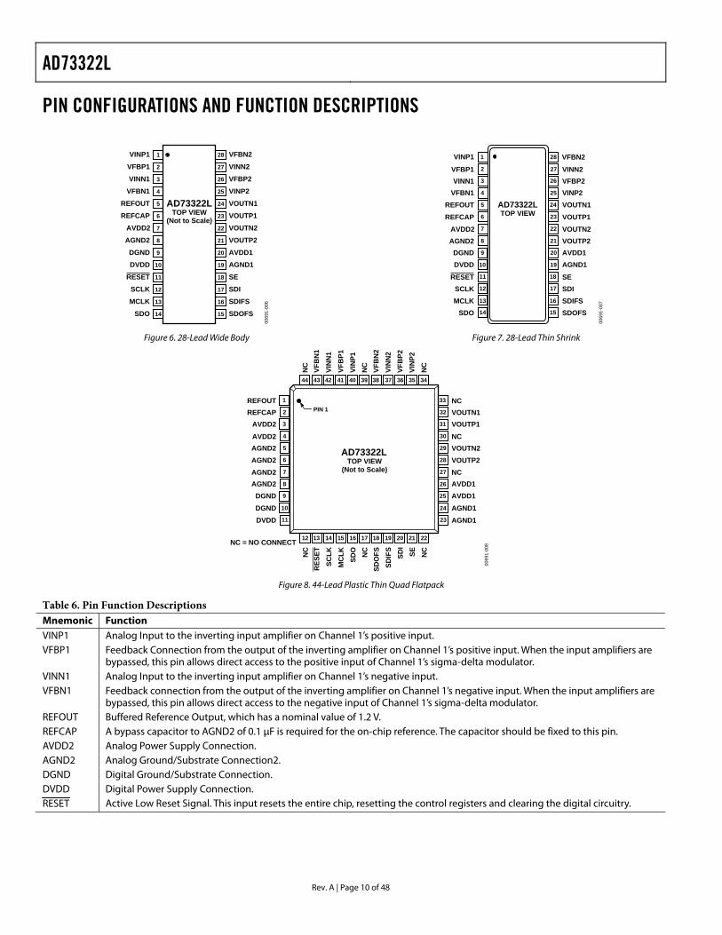
PIN CONFIGURATIONS AND FUNCTION DESCRIPTIONS
0069
1-00
6
VFBN228
VINN227
VFBP226
VINP225
VOUTN124
VOUTP123
VOUTN222
VOUTP221
AVDD120
AGND119
SE18
SDI17
SDIFS16
SDOFS15
VINP1 1
VFBP1 2
VINN1 3
VFBN1 4
REFOUT 5
REFCAP 6
AVDD2 7
AGND2 8
DGND 9
DVDD 10
RESET 11
SCLK 12
MCLK 13
SDO 14
AD73322LTOP VIEW
(Not to Scale)
Figure 6. 28-Lead Wide Body
0069
1-00
7
1
2
3
4
5
6
7
8
9
10
11
12
13
14
28
27
26
25
24
23
22
21
20
19
18
17
16
15
AD73322LTOP VIEW
VFBP1VINN1
VFBN1
AVDD2REFCAPREFOUT
VINP1
VINN2VFBP2VINP2
VOUTN2VOUTP1VOUTN1
AGND2DGNDDVDD
SDO
SCLKRESET
VOUTP2AVDD1AGND1
SDOFSMCLK SDIFS
SDISE
VFBN2
Figure 7. 28-Lead Thin Shrink
0069
1-00
8
44
NC
43
VFB
N1
42
VIN
N1
41
VFB
P1
40
VIN
P1
39
NC
38VF
BN
237
VIN
N2
36
VFB
P2
35
VIN
P2
34
NC
32 VOUTN131 VOUTP130 NC
27 NC
28 VOUTP2
29 VOUTN2
33 NC
26 AVDD125 AVDD124 AGND123 AGND1
2REFCAP3AVDD24AVDD2
7AGND2
6AGND2
5AGND2
1REFOUT
8AGND29DGND10DGND11DVDD
NC = NO CONNECT 12
NC
13
RES
ET
14
SCLK
15
MC
LK
16
SDO
17
NC
18
SDO
FS
19
SDIF
S
20
SDI
21
SE
22
NC
PIN 1
AD73322LTOP VIEW
(Not to Scale)
Figure 8. 44-Lead Plastic Thin Quad Flatpack
Table 6. Pin Function Descriptions Mnemonic Function VINP1 Analog Input to the inverting input amplifier on Channel 1’s positive input. VFBP1 Feedback Connection from the output of the inverting amplifier on Channel 1’s positive input. When the input amplifiers are
bypassed, this pin allows direct access to the positive input of Channel 1’s sigma-delta modulator. VINN1 Analog Input to the inverting input amplifier on Channel 1’s negative input. VFBN1 Feedback connection from the output of the inverting amplifier on Channel 1’s negative input. When the input amplifiers are
bypassed, this pin allows direct access to the negative input of Channel 1’s sigma-delta modulator. REFOUT Buffered Reference Output, which has a nominal value of 1.2 V. REFCAP A bypass capacitor to AGND2 of 0.1 µF is required for the on-chip reference. The capacitor should be fixed to this pin. AVDD2 Analog Power Supply Connection. AGND2 Analog Ground/Substrate Connection2. DGND Digital Ground/Substrate Connection. DVDD Digital Power Supply Connection. RESET Active Low Reset Signal. This input resets the entire chip, resetting the control registers and clearing the digital circuitry.
AD73322L
Rev. A | Page 11 of 48
Mnemonic Function SCLK Serial Clock Output. This rate determines the serial transfer rate to/from the codec. It is used to clock data or control
information to and from the serial port (SPORT). The frequency of SCLK is equal to the frequency of the master clock (MCLK) divided by an integer number—this integer number being the product of the external master clock rate divider and the serial clock rate divider.
MCLK Master Clock Input. MCLK is driven from an external clock signal. SDO Serial Data Output. Both data and control information may be output on this pin and are clocked on the positive edge of
SCLK. SDO is in three-state when no information is being transmitted and when SE is low. SDOFS Framing Signal Output for SDO Serial Transfers. The frame sync is one bit wide and is active one SCLK period before the first
bit (MSB) of each output word. SDOFS is referenced to the positive edge of SCLK. SDOFS is in three-state when SE is low. SDIFS Framing Signal Input for SDI Serial Transfers. The frame sync is one bit wide and is valid one SCLK period before the first bit
(MSB) of each input word. SDIFS is sampled on the negative edge of SCLK and is ignored when SE is low. SDI Serial Data Input. Both data and control information may be input on this pin and are clocked on the negative edge of SCLK.
SDI is ignored when SE is low. SE SPORT Enable. Asynchronous input enable pin for the SPORT. When SE is set low by the DSP, the output pins of the SPORT are
three-stated and the input pins are ignored. SCLK is also disabled internally in order to decrease power dissipation. When SE is brought high, the control and data registers of the SPORT are at their original values (before SE was brought low); however, the timing counters and other internal registers are at their reset values.
AGND1 Analog Ground/Substrate Connection. AVDD1 Analog Power Supply Connection. VOUTP2 Analog Output from the Positive Terminal of Output Channel 2. VOUTN2 Analog Output from the Negative Terminal of Output Channel 2. VOUTP1 Analog Output from the Positive Terminal of Output Channel 1. VOUTN1 Analog Output from the Negative Terminal of Output Channel 1. VINP2 Analog Input to the inverting input amplifier on Channel 2’s positive input. VFBP2 Feedback connection from the output of the inverting amplifier on Channel 2’s positive input. When the input amplifiers are
bypassed, this pin allows direct access to the positive input of Channel 2’s sigma-delta modulator. VINN2 Analog Input to the inverting input amplifier on Channel 2’s negative input. VFBN2 Feedback connection from the output of the inverting amplifier on Channel 2’s negative input. When the input amplifiers are
bypassed, this pin allows direct access to the negative input of Channel 2’s sigma-delta modulator.

AD73322L
Rev. A | Page 12 of 48
TERMINOLOGY Absolute Gain A measure of converter gain for a known signal. Absolute gain is measured (differentially) with a 1 kHz sine wave at 0 dBm0 for the DAC and with a 1 kHz sine wave at 0 dBm0 for the ADC. The absolute gain specification is used for gain tracking error specification.
Crosstalk Crosstalk is due to coupling of signals from a given channel to an adjacent channel. It is defined as the ratio of the amplitude of the coupled signal to the amplitude of the input signal. Crosstalk is expressed in dB.
Gain Tracking Error Measures changes in converter output for different signal levels relative to an absolute signal level. The absolute signal level is 0 dBm0 (equal to absolute gain) at 1 kHz for the DAC and 0 dBm0 (equal to absolute gain) at 1 kHz for the ADC. Gain tracking error at 0 dBm0 (ADC) and 0 dBm0 (DAC) is 0 dB by definition.
Group Delay The derivative of radian phase with respect to radian frequency, dø(f)/df. Group delay is a measure of the average delay of a system as a function of frequency. A linear system with a constant group delay has a linear phase response. The deviation of group delay from a constant indicates the degree of nonlinear phase response of the system.
Idle Channel Noise The total signal energy measured at the output of the device when the input is grounded (measured in the frequency range 300 Hz to 3400 Hz).
Intermodulation Distortion With inputs consisting of sine waves at two frequencies, fa and fb, any active device with nonlinearities creates distortion products at sum and difference frequencies of mfa ± nfb where m, n = 0, 1, 2, 3, etc. Intermodulation terms are those for which neither m nor n is equal to zero. For final testing, the second-order terms include (fa + fb) and (fa − fb), while the third-order terms include (2fa + fb), (2fa − fb), (fa + 2fb) and (fa − 2fb).
Power Supply Rejection Measures the susceptibility of a device to noise on the power supply. Power supply rejection is measured by modulating the power supply with a sine wave and measuring the noise at the output (relative to 0 dB).
Sample Rate The rate at which the ADC updates its output register and the DAC updates its output from its input register. The sample rate can be chosen from a list of four that are fixed relative to the DMCLK. Sample rate is set by programming bits DIR0-1 in Control Register B of each channel.
SNR + THD Signal-to-noise ratio plus harmonic distortion is the ratio of the rms value of the measured input signal to the rms sum of all other spectral components in the frequency range 300 Hz to 3400 Hz, including harmonics but excluding dc.
ABBREVIATIONS Table 7. Abbreviation Definition ADC Analog-to-digital converter. AFE Analog front end. AGT Analog gain tap. ALB Analog loop-back. BW Bandwidth. CRx A control register where x is a placeholder for
an alphabetic character (A to H). There are eight read/write control registers on the AD73322L—CRA through CRH.
CRx:n A bit position, where n is a placeholder for a numeric character (0 to 7), within a control register, where x is a placeholder for an alphabetic character (A to E). Position 7 represents the MSB and Position 0 represents the LSB.
DAC Digital-to-analog converter. DGT Digital gain tap. DLB Digital loop-back. DMCLK Device (internal) master clock. This is the
internal master clock resulting from the external master clock (MCLK) being divided by the on-chip master clock divider.
FS Full scale. FSLB Frame sync loop-back—where the SDOFS of
the final device in a cascade is connected to the RFS and TFS of the DSP and the SDIFS of first device in the cascade. Data input and output occur simultaneously. In the case of nonFSLB, SDOFS and SDO are connected to the Rx port of the DSP while SDIFS and SDI are connected to the Tx port.
PGA Programmable gain amplifier. SC Switched capacitor. SLB SPORT loop-back. SNR Signal-to-noise ratio. SPORT Serial port. THD Total harmonic distortion. VBW Voice bandwidth.
AD73322L
Rev. A | Page 13 of 48
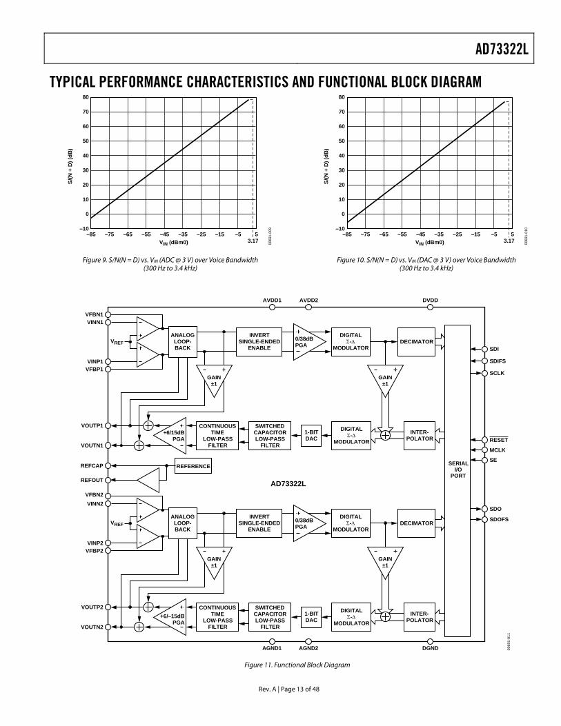
TYPICAL PERFORMANCE CHARACTERISTICS AND FUNCTIONAL BLOCK DIAGRAM
0069
1-00
9
VIN (dBm0)5
3.17–85 –75 –65 –55 –45 –35 –25 –15 –5
S/(N
+ D
) (dB
)
80
60
70
50
30
40
10
20
0
–10
Figure 9. S/N(N = D) vs. VIN (ADC @ 3 V) over Voice Bandwidth (300 Hz to 3.4 kHz)
0069
1-01
0
VIN (dBm0)5
3.17–85 –75 –65 –55 –45 –35 –25 –15 –5
S/(N
+ D
) (dB
)
80
60
70
50
30
40
10
20
0
–10
Figure 10. S/N(N = D) vs. VIN (DAC @ 3 V) over Voice Bandwidth (300 Hz to 3.4 kHz)
INVERTSINGLE-ENDED
ENABLEDECIMATOR
SERIALI/O
PORT
CONTINUOUSTIME
LOW-PASSFILTER
1-BITDAC
SWITCHEDCAPACITORLOW-PASS
FILTER
DIGITALΣ-∆
MODULATOR
DIGITALΣ-∆
MODULATOR
INTER-POLATOR
VREF
VFBN1VINN1
VINP1VFBP1
VOUTP1
VOUTN1
AD73322L
AGND1 AGND2 DGND
SDOFS
SDO
MCLK
SE
RESET
SCLK
SDIFS
SDI
DVDDAVDD2AVDD1
ANALOGLOOP-BACK
+6/15dBPGA
0/38dBPGA
GAIN±1
GAIN±1
INVERTSINGLE-ENDED
ENABLEDECIMATOR
CONTINUOUSTIME
LOW-PASSFILTER
1-BITDAC
SWITCHEDCAPACITORLOW-PASS
FILTER
DIGITALΣ-∆
MODULATOR
DIGITALΣ-∆
MODULATOR
INTER-POLATOR
VREF
REFCAP
REFOUT
REFERENCE
VFBN2VINN2
VINP2VFBP2
VOUTP2
VOUTN2
ANALOGLOOP-BACK
+6/–15dBPGA
0/38dBPGA
GAIN±1
GAIN±1
0069
1-01
1
Figure 11. Functional Block Diagram
AD73322L
Rev. A | Page 14 of 48
FUNCTIONAL DESCRIPTIONS ENCODER CHANNELSBoth encoder channels consist of a pair of inverting op amps with feedback connections that can be bypassed if required, a switched capacitor PGA and a sigma-delta analog-to-digital converter (ADC). An on-board digital filter, which forms part of the sigma-delta ADC, also performs critical system-level filtering. Due to the high level of oversampling, the input antialias requirements are reduced such that a simple single-pole RC stage is sufficient to give adequate attenuation in the band of interest.
PROGRAMMABLE GAIN AMPLIFIER Each encoder section’s analog front end comprises a switched capacitor PGA, which also forms part of the sigma-delta modulator. The SC sampling frequency is DMCLK/8. The PGA, whose programmable gain settings are shown in Table 8, may be used to increase the signal level applied to the ADC from low output sources such as microphones, and can be used to avoid placing external amplifiers in the circuit. The input signal level to the sigma-delta modulator should not exceed the maximum input voltage permitted.
The PGA gain is set by bits IGS0, IGS1, and IGS2 (CRD:0–2) in control register D.
Table 8. PGA Settings for the Encoder Channel IGS2 IGS1 IGS0 Gain (dB) 0 0 0 0 0 0 1 6 0 1 0 12 0 1 1 18 1 0 0 20 1 0 1 26 1 1 0 32 1 1 1 38
ADC Both ADCs consist of an analog sigma-delta modulator and a digital antialiasing decimation filter. The sigma-delta modulator noise-shapes the signal and produces 1-bit samples at a DMCLK/8 rate. This bit stream, representing the analog input signal, is input to the antialiasing decimation filter. The decimation filter reduces the sample rate and increases the resolution.
ANALOG SIGMA-DELTA MODULATOR The AD73322L’s input channels employ a sigma-delta conversion technique, which provides a high resolution 16-bit output with system filtering being implemented on-chip.
Sigma-delta converters employ a technique known as oversampling, where the sampling rate is many times the
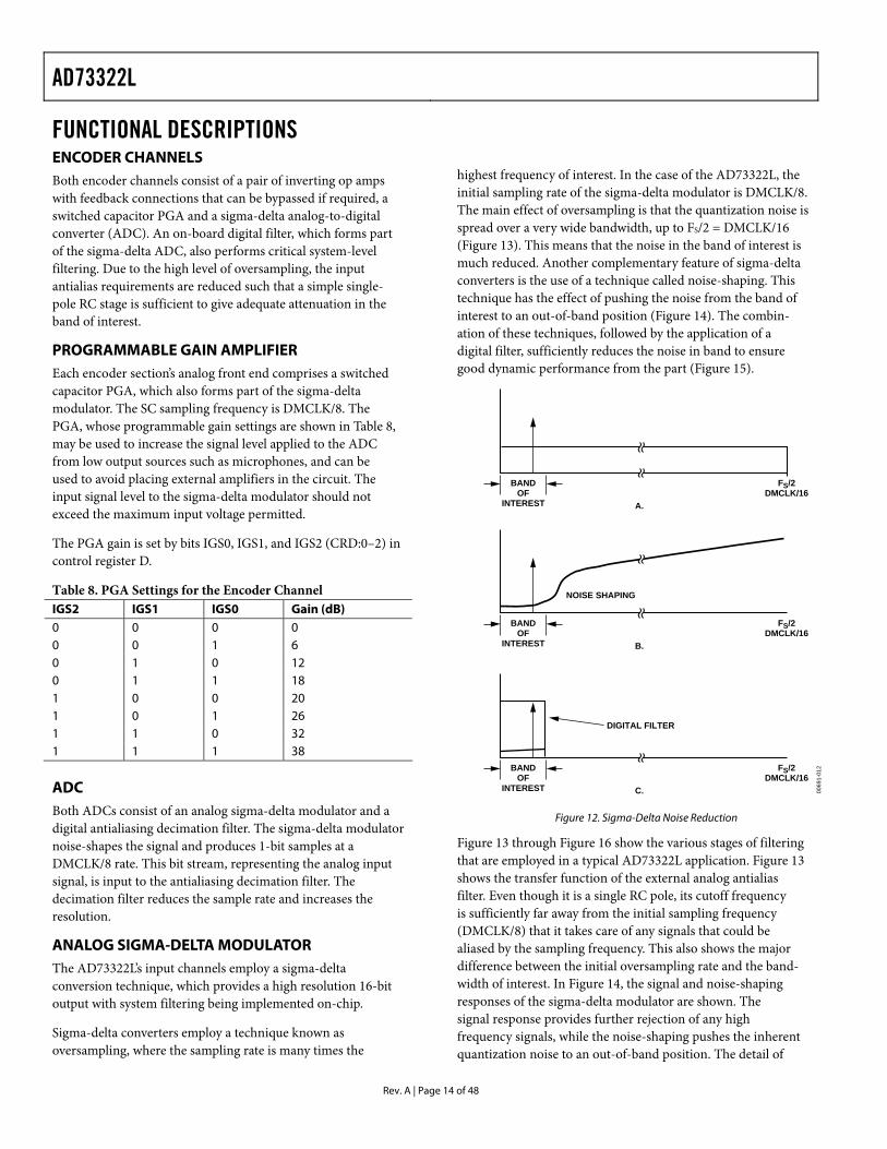
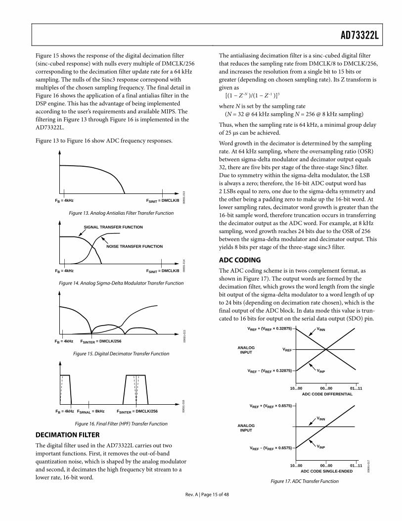
highest frequency of interest. In the case of the AD73322L, the initial sampling rate of the sigma-delta modulator is DMCLK/8. The main effect of oversampling is that the quantization noise is spread over a very wide bandwidth, up to FS/2 = DMCLK/16 (Figure 13). This means that the noise in the band of interest is much reduced. Another complementary feature of sigma-delta converters is the use of a technique called noise-shaping. This technique has the effect of pushing the noise from the band of interest to an out-of-band position (Figure 14). The combin-ation of these techniques, followed by the application of a digital filter, sufficiently reduces the noise in band to ensure good dynamic performance from the part (Figure 15).
FS/2DMCLK/16
DIGITAL FILTER
NOISE SHAPING
A.
0069
1-01
2
BANDOF
INTEREST
FS/2DMCLK/16
B.
BANDOF
INTEREST
FS/2DMCLK/16
C.
BANDOF
INTEREST
Figure 12. Sigma-Delta Noise Reduction
Figure 13 through Figure 16 show the various stages of filtering that are employed in a typical AD73322L application. Figure 13 shows the transfer function of the external analog antialias filter. Even though it is a single RC pole, its cutoff frequency is sufficiently far away from the initial sampling frequency (DMCLK/8) that it takes care of any signals that could be aliased by the sampling frequency. This also shows the major difference between the initial oversampling rate and the band-width of interest. In Figure 14, the signal and noise-shaping responses of the sigma-delta modulator are shown. The signal response provides further rejection of any high frequency signals, while the noise-shaping pushes the inherent quantization noise to an out-of-band position. The detail of
AD73322L
Rev. A | Page 15 of 48
Figure 15 shows the response of the digital decimation filter (sinc-cubed response) with nulls every multiple of DMCLK/256 corresponding to the decimation filter update rate for a 64 kHz sampling. The nulls of the Sinc3 response correspond with multiples of the chosen sampling frequency. The final detail in Figure 16 shows the application of a final antialias filter in the DSP engine. This has the advantage of being implemented according to the user’s requirements and available MIPS. The filtering in Figure 13 through Figure 16 is implemented in the AD73322L.
Figure 13 to Figure 16 show ADC frequency responses.
FB = 4kHz FSINIT = DMCLK/8
0069
1-01
3
Figure 13. Analog Antialias Filter Transfer Function
NOISE TRANSFER FUNCTION
SIGNAL TRANSFER FUNCTION
0069
1-01
4
FB = 4kHz FSINIT = DMCLK/8
Figure 14. Analog Sigma-Delta Modulator Transfer Function
0069
1-01
5
FB = 4kHz FSINTER = DMCLK/256
Figure 15. Digital Decimator Transfer Function
0069
1-01
6
FB = 4kHz FSRNAL = 8kHz FSINTER = DMCLK/256
Figure 16. Final Filter (HPF) Transfer Function
DECIMATION FILTER The digital filter used in the AD73322L carries out two important functions. First, it removes the out-of-band quantization noise, which is shaped by the analog modulator and second, it decimates the high frequency bit stream to a lower rate, 16-bit word.
The antialiasing decimation filter is a sinc-cubed digital filter that reduces the sampling rate from DMCLK/8 to DMCLK/256, and increases the resolution from a single bit to 15 bits or greater (depending on chosen sampling rate). Its Z transform is given as
[(1 − Z−N )/(1 − Z−1 )]3
where N is set by the sampling rate (N = 32 @ 64 kHz sampling N = 256 @ 8 kHz sampling)
Thus, when the sampling rate is 64 kHz, a minimal group delay of 25 µs can be achieved.
Word growth in the decimator is determined by the sampling rate. At 64 kHz sampling, where the oversampling ratio (OSR) between sigma-delta modulator and decimator output equals 32, there are five bits per stage of the three-stage Sinc3 filter. Due to symmetry within the sigma-delta modulator, the LSB is always a zero; therefore, the 16-bit ADC output word has 2 LSBs equal to zero, one due to the sigma-delta symmetry and the other being a padding zero to make up the 16-bit word. At lower sampling rates, decimator word growth is greater than the 16-bit sample word, therefore truncation occurs in transferring the decimator output as the ADC word. For example, at 8 kHz sampling, word growth reaches 24 bits due to the OSR of 256 between the sigma-delta modulator and decimator output. This yields 8 bits per stage of the three-stage sinc3 filter.
ADC CODING The ADC coding scheme is in twos complement format, as shown in Figure 17). The output words are formed by the decimation filter, which grows the word length from the single bit output of the sigma-delta modulator to a word length of up to 24 bits (depending on decimation rate chosen), which is the final output of the ADC block. In data mode this value is trun-cated to 16 bits for output on the serial data output (SDO) pin.
VREF + (VREF × 0.32875)
VREF
VREF – (VREF × 0.32875)
10...00 00...00 01...11ADC CODE DIFFERENTIAL
ANALOGINPUT
ANALOGINPUT
VINN
VINP
VREF + (VREF × 0.6575)
VREF – (VREF × 0.6575)
10...00 00...00 01...11ADC CODE SINGLE-ENDED
VINP
VINN
0069
1-01
7
Figure 17. ADC Transfer Function
AD73322L
Rev. A | Page 16 of 48
In mixed control/data mode, the resolution is fixed at 15 bits, with the MSB of the 16-bit transfer being used as a flag bit to indicate either control or data in the frame.
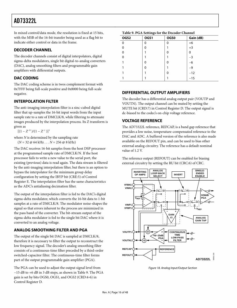
DECODER CHANNEL The decoder channels consist of digital interpolators, digital sigma-delta modulators, single bit digital-to-analog converters (DAC), analog smoothing filters and programmable gain amplifiers with differential outputs.
DAC CODING The DAC coding scheme is in twos complement format with 0x7FFF being full-scale positive and 0x8000 being full-scale negative.
INTERPOLATION FILTER The anti-imaging interpolation filter is a sinc-cubed digital filter that up-samples the 16-bit input words from the input sample rate to a rate of DMCLK/8, while filtering to attenuate images produced by the interpolation process. Its Z transform is given as
[(1 − Z−N )/(1 − Z−1 )]3
where N is determined by the sampling rate (N = 32 @ 64 kHz . . . N = 256 @ 8 kHz)
The DAC receives 16-bit samples from the host DSP processor at the programmed sample rate of DMCLK/N. If the host processor fails to write a new value to the serial port, the existing (previous) data is read again. The data stream is filtered by the anti-imaging interpolation filter, but there is an option to bypass the interpolator for the minimum group delay configuration by setting the IBYP bit (CRE:5) of Control Register E. The interpolation filter has the same characteristics as the ADC’s antialiasing decimation filter.
The output of the interpolation filter is fed to the DAC’s digital sigma-delta modulator, which converts the 16-bit data to 1-bit samples at a rate of DMCLK/8. The modulator noise-shapes the signal so that errors inherent to the process are minimized in the pass band of the converter. The bit-stream output of the sigma-delta modulator is fed to the single bit DAC where it is converted to an analog voltage.
ANALOG SMOOTHING FILTER AND PGA The output of the single bit DAC is sampled at DMCLK/8, therefore it is necessary to filter the output to reconstruct the low frequency signal. The decoder’s analog smoothing filter consists of a continuous-time filter preceded by a third-order switched-capacitor filter. The continuous-time filter forms part of the output programmable gain amplifier (PGA).
The PGA can be used to adjust the output signal level from −15 dB to +6 dB in 3 dB steps, as shown in Table 9. The PGA gain is set by bits OGS0, OGS1, and OGS2 (CRD:4-6) in Control Register D.
Table 9. PGA Settings for the Decoder Channel OGS2 OGS1 OGS0 Gain (dB) 0 0 0 +6 0 0 1 +3 0 1 0 0 0 1 1 −3
1 0 0 −6
1 0 1 −9
1 1 0 −12
1 1 1 −15
DIFFERENTIAL OUTPUT AMPLIFIERS The decoder has a differential analog output pair (VOUTP and VOUTN). The output channel can be muted by setting the MUTE bit (CRD:7) in Control Register D. The output signal is dc-biased to the codec’s on-chip voltage reference.
VOLTAGE REFERENCE The AD73322L reference, REFCAP, is a band gap reference that provides a low noise, temperature-compensated reference to the DAC and ADC. A buffered version of the reference is also made available on the REFOUT pin, and can be used to bias other external analog circuitry. The reference has a default nominal value of 1.2 V.
The reference output (REFOUT) can be enabled for biasing external circuitry by setting the RU bit (CRC:6) of CRC.
INVERTINGOP AMPS
ANALOGGAIN TAP
ANALOGLOOP-BACK
SELECT INVERTSINGLE-ENDED
ENABLE
0069
1-01
8
CONTINUOUSTIME
LOW-PASSFILTER
VREF
VFBN1VINN1
VINP1VFBP1
VOUTP1
VOUTN1
AD73322L
+6/–15dBPGA
0/38dBPGA
GAIN±1
REFCAP
REFOUT
REFERENCE
VREF
Figure 18. Analog Input/Output Section
AD73322L
Rev. A | Page 17 of 48
MCLKDIVIDER
MCLKEXTERNAL
SERESETSDIFS
SDI
SERIAL PORT 1(SPORT 1)
SERIAL REGISTER 1
SCLKDIVIDER
SCLK
CONTROLREGISTER
1A
CONTROLREGISTER
1B
CONTROLREGISTER
1G
CONTROLREGISTER
1H
CONTROLREGISTER
1F
CONTROLREGISTER
1C
CONTROLREGISTER
1D
DMCLK INTERNAL
SDOFS1SDO1
0069
1-01
9
8
3 3
16 8
28
8 88
CONTROLREGISTER
1E
MCLKDIVIDER
MCLKEXTERNAL
SERESET
SDIFS2SDI2
SERIAL PORT 2(SPORT 1)
SERIAL REGISTER 2
SCLKDIVIDER
SCLK
CONTROLREGISTER
2A
CONTROLREGISTER
2B
CONTROLREGISTER
2G
CONTROLREGISTER
2H
CONTROLREGISTER
2F
CONTROLREGISTER
2C
CONTROLREGISTER
2D
DMCLK INTERNAL
SDOFSSDO
8
16 8
2
8
8 88
CONTROLREGISTER
2E
Figure 19. SPORT Block Diagram
ANALOG AND DIGITAL GAIN TAPS The AD73322L features analog and digital feedback paths between input and output. The amount of feedback is deter-mined by the gain setting which is programmed in the control registers. This feature can typically be used for balancing the effective impedance between input and output when used in subscriber line interface circuit (SLIC) interfacing.
Analog Gain Tap
The analog gain tap is configured as a programmable differential amplifier whose input is taken from the ADC’s input signal path. The output of the analog gain tap is summed with the output of the DAC. The gain is programmable using Control Register F (CRF:0-4) to achieve a gain of −1 to +1 in 32 steps with muting being achieved through a separate control setting (Control Register F Bit 7). The gain increment per step is 0.0625. The AGT is enabled by powering-up the AGT control bit in the power control register (CRC:1). When this bit is set (=1), CRF becomes an AGT control register with CRF:0-4 holding the AGT coefficient, CRF:5 becomes an AGT enable and CRF:7 becomes an AGT mute control bit.
Control bit CRF:5 connects/disconnects the AGT output to the summer block at the output of the DAC section while control bit CRF:7 overrides the gain tap setting with a mute, (zero gain) setting. Table 10 shows the gain vs. digital setting for the AGT. In this table, AGT and DGT weights are given for the case of VFBNx (connected to the sigma-delta modulator’s positive input) being at a higher potential than VFBPx (connected to the sigma-delta modulator’s negative input).
Table 10. Analog Gain Tap Settings AGTC4 AGTC3 AGTC2 AGTC1 AGTC0 Gain (dB) 0 0 0 0 0 1.00 0 0 0 0 1 0.9375 0 0 0 1 0 0.875 0 0 0 1 1 0.8125 0 0 1 0 0 0.75 0 1 1 1 1 0.0625 1 0 0 0 0 −0.0625 1 1 1 0 1 −0.875 1 1 1 1 0 −0.9375 1 1 1 1 1 −1.00

AD73322L
Rev. A | Page 18 of 48
DIGITAL GAIN TAP The digital gain tap features a programmable gain block whose input is taken from the bit stream output of the ADC’s sigma delta modulator. This single bit input (1 or 0) is used to add or subtract a programmable value, which is the digital gain tap setting, to the output of the DAC section’s interpolator. The programmable setting has 16-bit resolution and is programmed using the settings in Control Registers G and H, as shown in Table 11. In this table, AGT and DGT weights are given for the case of VFBNx (connected to the sigma-delta modulator’s positive input) being at a higher potential than VFBPx (connected to the sigma-delta modulator’s negative input).
Table 11. Digital Gain Tap Settings DGT15–0 (Hex) Gain 0x8000 −1.00 0x9000 −0.875 0xA000 −0.75 0xC000 −0.5 0xE000 −0.25 0x0000 0.00 0x2000 +0.25 0x4000 +0.05 0x6000 +0.75 0x7FFF +0.99999
SERIAL PORT (SPORT) The codecs communicate with a host processor via the bidirectional synchronous serial port (SPORT), which is compatible with most modern DSPs. The SPORT is used to transmit and receive digital data and control information. The dual codec is implemented using two separate codec blocks that are internally cascaded with serial port access to the input of Codec 1 and the output of Codec 2. This allows other single or dual codec devices to be cascaded together (up to a limit of eight codec units).
In both transmit and receive modes, data is transferred at the serial clock (SCLK) rate with the MSB being transferred first. Due to the fact that the SPORT of each codec block uses a common serial register for serial input and output, commun-ications between an AD73322L codec and a host processor (DSP engine) must always be initiated by the codecs themselves. In this configuration, the codecs are described as being in master mode. This ensures that there is no collision between input data and output samples.
SPORT OVERVIEW The AD73322L SPORT is a flexible, full-duplex, synchronous serial port having a protocol designed to allow up to four AD73322L devices (or combinations of AD73322L dual codecs and AD73311 single codecs up to eight codec blocks) to be connected, in cascade, to a single DSP via a 6-wire interface. It has a very flexible architecture that can be configured by programming two of the internal control registers in each codec block. The device has three distinct modes of operation: control mode, data mode, and mixed control/data mode.
Note that because each codec has its own SPORT section, the register settings in both SPORTs must be programmed. The registers that control SPORT and sample rate operation (CRA and CRB) must be programmed with the same values, otherwise incorrect operation may occur.
In control mode (CRA:0 = 0), the device’s internal configuration can be programmed by writing to the eight internal control registers. In this mode, control information can be written to or read from the codec. In data mode (CRA:0 = 1), (CRA:1 = 0), information sent to the device is used to update the decoder section (DAC), while the encoder section (ADC) data is read from the device. In this mode, only DAC and ADC data are written to or read from the device. Mixed mode (CRA:0 = 1 and CRA:1 = 1) allows the user to choose whether the infor-mation being sent to the device contains control information or DAC data. This is achieved by using the MSB of the 16-bit frame as a flag bit. Mixed mode reduces the resolution to 15 bits with the MSB being used to indicate whether the information in the 16-bit frame is control information or DAC/ADC data.
The SPORT features a single 16-bit serial register that is used for both input and output data transfers. As the input and output data must share the same register, some precautions must be observed. The primary precaution is that no informa-tion must be written to the SPORT without reference to an output sample event, which is when the serial register is overwritten with the latest ADC sample word. Once the SPORT starts to output the latest ADC word, it is safe for the DSP to write new control or data-words to the codec. In certain con-figurations, data can be written to the device to coincide with the output sample being shifted out of the serial register — see the Interfacing section. The serial clock rate (CRB:2–3) defines how many 16-bit words can be written to a device before the next output sample event happens.
AD73322L
Rev. A | Page 19 of 48
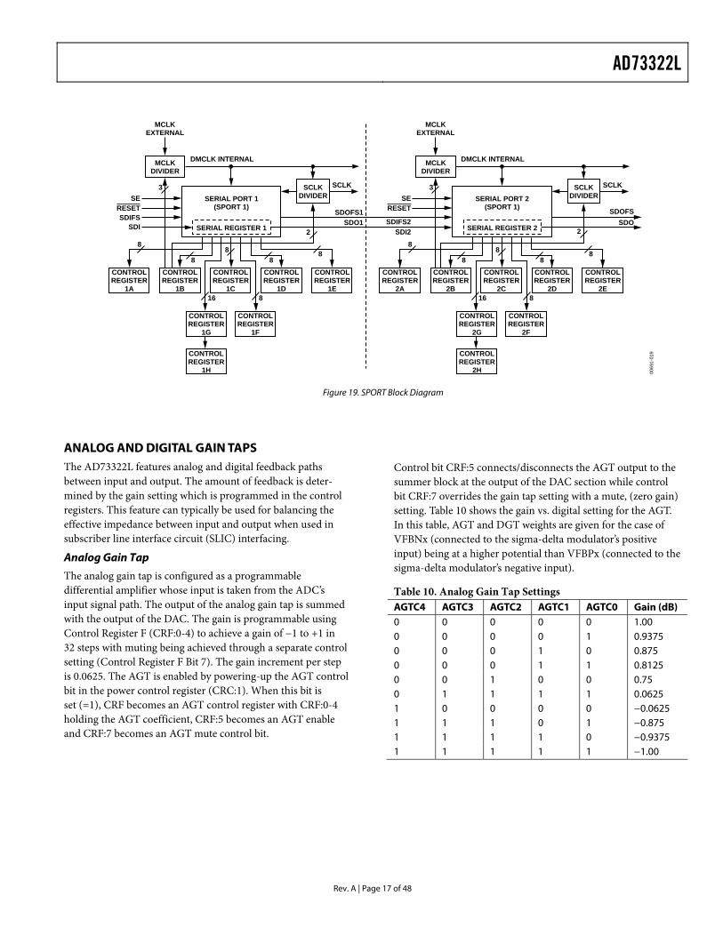
The SPORT block diagram shown in Figure 19 details the blocks associated with Codecs 1 and 2, including the eight control registers (A–H), external MCLK to internal DMCLK divider, and serial clock divider. The divider rates are controlled by the setting of Control Register B. The AD73322L features a master clock divider that allows users the flexibility of dividing externally available high frequency DSP or CPU clocks to generate a lower frequency master clock internally in the codec, which may be more suitable for either serial transfer or sampling rate requirements. The master clock divider has five divider options (÷1 default condition, ÷2, ÷3, ÷4, ÷5) that are set by loading the master clock divider field in Register B with the appropriate code (see ). Once the internal device master clock (DMCLK) has been set using the master clock divider, the sample rate and serial clock settings are derived from DMCLK.
The SPORT can work at four different serial clock (SCLK) rates chosen from DMCLK, DMCLK/2, DMCLK/4, or DMCLK/8, where DMCLK is the internal or device master clock resulting from the external or pin master clock being divided by the master clock divider.
SPORT REGISTER MAPS There are two register banks for each codec in the AD73322L, the control register bank and the data register bank. The control register bank consists of eight read/write registers, each eight bits wide. Table 16 shows the control register map for the AD73322L. The first two control registers, CRA and CRB, are reserved for controlling the SPORT. They hold settings for parameters such as serial clock rate, internal master clock rate, sample rate and device count. As both codecs are internally cascaded, registers CRA and CRB on each codec must be programmed with the same setting to ensure correct operation (this is shown in the programming examples).
The other five registers, CRC through CRH, are used to hold control settings for the ADC, DAC, reference, power control, and gain tap sections of the device. It is not necessary for the contents of CRC through CRH on each codec be similar. Control registers are written to on the negative edge of SCLK. The data register bank consists of two, 16-bit registers that are the DAC and ADC registers.
MASTER CLOCK DIVIDER The AD73322L features a programmable master clock divider that allows the user to reduce an externally available master clock, at pin MCLK, by a ratio of 1, 2, 3, 4, or 5 to produce an internal master clock signal (DMCLK) that is used to calculate the sampling and serial clock rates. The master clock divider is programmable by setting CRB:4-6. Table 12 shows the division ratio corresponding to the various bit settings. The default divider ratio is divide-by-one.
Table 12. DMCLK (Internal) Rate Divider Settings MCD2 MCD1 MCD0 DMCLK Rate 0 0 0 MCLK 0 0 1 MCLK/2 0 1 0 MCLK/3 0 1 1 MCLK/4 1 0 0 MCLK/5 1 0 1 MCLK 1 1 0 MCLK 1 1 1 MCLK
SERIAL CLOCK RATE DIVIDER The AD73322L features a programmable serial clock divider that allows users to match the serial clock (SCLK) rate of the data to that of the DSP engine or host processor. The maximum SCLK rate available is DMCLK, and the other available rates are DMCLK/2, DMCLK/4, and DMCLK/8. The slowest rate (DMCLK/8) is the default SCLK rate. The serial clock divider is programmable by setting bits CRB:2–3. Table 13 shows the serial clock rate corresponding to the various bit settings.
Table 13. SCLK Rate Divider Settings SCD1 SCD0 SCLK Rate 0 0 DMCLK/8 0 1 DMCLK/4 1 0 DMCLK/2 1 1 DMCLK
SAMPLE RATE DIVIDER The AD73322L features a programmable sample rate divider that allows users flexibility in matching the codec’s ADC and DAC sample rates (decimation/interpolation rates) to the needs of the DSP software. The maximum sample rate available is DMCLK/256, which offers the lowest conversion group delay, while the other available rates are DMCLK/512, DMCLK/1024, and DMCLK/2048. The slowest rate (DMCLK/2048) is the default sample rate. The sample rate divider is programmable by setting bits CRB:0-1. Table 14 shows the sample rate corresponding to the various bit settings.
Table 14. Sample Rate Divider Settings DIR1 DIR0 SCLK Rate 0 0 DMCLK/2048 0 1 DMCLK/1024 1 0 DMCLK/512 1 1 DMCLK/256
AD73322L
Rev. A | Page 20 of 48
DAC ADVANCE REGISTERThe loading of the DAC is internally synchronized with the unloading of the ADC data in each sampling interval. The default DAC load event happens one SCLK cycle before the SDOFS flag is raised by the ADC data being ready. However, this DAC load position can be advanced before this time by modifying the contents of the DAC advance field in Control Register E (CRE:0–4). The field is five bits wide, allowing 31 increments of weight 1/(FS × 32), as shown in Table 15.
The sample rate, fS, depends on the setting of both the MCLK divider and the sample rate divider, as shown in Table 12 and Table 14. In certain circumstances this DAC update adjustment can reduce the group delay when the ADC and DAC are used to process data in series. For more information about how the DAC advance register can be used, see the section Configuring an AD73322L to Operate in Mixed Mode.
NOTE: The DAC advance register should not be changed while the DAC section is powered up.
Table 15. DAC Timing Control DA4 DA3 DA2 DA1 DA0 Time Advance 0 0 0 0 0 0 s 0 0 0 0 1 1/(FS × 32) s 0 0 0 1 0 2/(FS × 32) s 1 1 1 1 0 30/(FS × 32) s 1 1 1 1 1 31/(FS × 32) s
Table 16. Control Register Map Address (Binary) Name Description Type Width Reset Setting (Hex) 000 CRA Control Register A R/W 8 0x00
001 CRB Control Register B R/W 8 0x00
010 CRC Control Register C R/W 8 0x00
011 CRD Control Register D R/W 8 0x00
100 CRE Control Register E R/W 8 0x00
101 CRF Control Register F R/W 8 0x00
110 CRG Control Register G R/W 8 0x00
111 CRH Control Register H R/W 8 0x00
Table 17. Control Word Description 15 14 13 12 11 10 9 8 7 6 5 4 3 2 1 0 C/D R/W Device Address Register Address Register Data
Control Frame Description Bit 15 Control/Data When set high, this bit signifies a control word in program or mixed program/data modes. When set
low, it signifies a data-word in mixed program/data mode or an invalid control word in program mode. Bit 14 Read/Write When set low, this bit tells the device that the data field is to be written to the register selected by the
register field setting, provided the address field is zero. When set high, it tells the device that the selected register is to be written to the data field in the input serial register and that the new control word is to be output from the device via the serial output.
Bits 13 to 11 Device Address This 3-bit field holds the address information. Only when this field is zero is a device selected. If the address is not zero, it is decremented and the control word is passed out of the device via the serial output.
Bits 10 to 8 Register Address This 3-bit field is used to select one of the eight control registers on the AD73322L. Bits 7 to 0 Register Data This 8-bit field holds the data that is to be written to or read from the selected register provided the
address field is zero.
AD73322L
Rev. A | Page 21 of 48
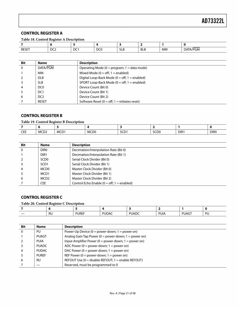
CONTROL REGISTER A Table 18. Control Register A Description 7 6 5 4 3 2 1 0 RESET DC2 DC1 DC0 SLB BLB MM DATA/PGM
Bit Name Description 0 DATA/PGM Operating Mode (0 = program; 1 = data mode)
1 MM Mixed Mode (0 = off; 1 = enabled) 2 DLB Digital Loop-Back Mode (0 = off; 1 = enabled) 3 SLB SPORT Loop-Back Mode (0 = off; 1 = enabled) 4 DC0 Device Count (Bit 0) 5 DC1 Device Count (Bit 1) 6 DC2 Device Count (Bit 2) 7 RESET Software Reset (0 = off; 1 = initiates reset)
CONTROL REGISTER B Table 19. Control Register B Description 7 6 5 4 3 2 1 0 CEE MCD2 MCD1 MCD0 SCD1 SCD0 DIR1 DIR0
Bit Name Description 0 DIR0 Decimation/Interpolation Rate (Bit 0) 1 DIR1 Decimation/Interpolation Rate (Bit 1) 2 SCD0 Serial Clock Divider (Bit 0) 3 SCD1 Serial Clock Divider (Bit 1) 4 MCD0 Master Clock Divider (Bit 0) 5 MCD1 Master Clock Divider (Bit 1) 6 MCD2 Master Clock Divider (Bit 2) 7 CEE Control Echo Enable (0 = off; 1 = enabled)
CONTROL REGISTER C Table 20. Control Register C Description 7 6 5 4 3 2 1 0 — RU PUREF PUDAC PUADC PUIA PUAGT PU
Bit Name Description 0 PU Power-Up Device (0 = power-down; 1 = power on) 1 PUAGT Analog Gain Tap Power (0 = power-down; 1 = power on) 2 PUIA Input Amplifier Power (0 = power-down; 1 = power on) 3 PUADC ADC Power (0 = power-down; 1 = power on) 4 PUDAC DAC Power (0 = power-down; 1 = power on) 5 PUREF REF Power (0 = power-down; 1 = power on) 6 RU REFOUT Use (0 = disable REFOUT; 1 = enable REFOUT) 7 — Reserved, must be programmed to 0
AD73322L
Rev. A | Page 22 of 48
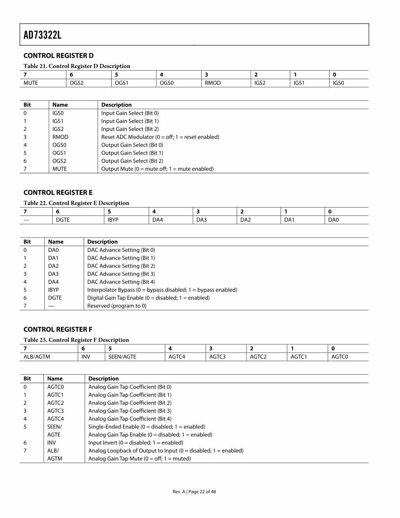
CONTROL REGISTER D Table 21. Control Register D Description 7 6 5 4 3 2 1 0 MUTE OGS2 OGS1 OGS0 RMOD IGS2 IGS1 IGS0
Bit Name Description 0 IGS0 Input Gain Select (Bit 0) 1 IGS1 Input Gain Select (Bit 1) 2 IGS2 Input Gain Select (Bit 2) 3 RMOD Reset ADC Modulator (0 = off; 1 = reset enabled) 4 OGS0 Output Gain Select (Bit 0) 5 OGS1 Output Gain Select (Bit 1) 6 OGS2 Output Gain Select (Bit 2) 7 MUTE Output Mute (0 = mute off; 1 = mute enabled)
CONTROL REGISTER E Table 22. Control Register E Description 7 6 5 4 3 2 1 0 — DGTE IBYP DA4 DA3 DA2 DA1 DA0
Bit Name Description 0 DA0 DAC Advance Setting (Bit 0) 1 DA1 DAC Advance Setting (Bit 1) 2 DA2 DAC Advance Setting (Bit 2) 3 DA3 DAC Advance Setting (Bit 3) 4 DA4 DAC Advance Setting (Bit 4) 5 IBYP Interpolator Bypass (0 = bypass disabled; 1 = bypass enabled) 6 DGTE Digital Gain Tap Enable (0 = disabled; 1 = enabled) 7 — Reserved (program to 0)
CONTROL REGISTER F Table 23. Control Register F Description 7 6 5 4 3 2 1 0 ALB/AGTM INV SEEN/AGTE AGTC4 AGTC3 AGTC2 AGTC1 AGTC0
Bit Name Description 0 AGTC0 Analog Gain Tap Coefficient (Bit 0) 1 AGTC1 Analog Gain Tap Coefficient (Bit 1) 2 AGTC2 Analog Gain Tap Coefficient (Bit 2) 3 AGTC3 Analog Gain Tap Coefficient (Bit 3) 4 AGTC4 Analog Gain Tap Coefficient (Bit 4) 5 SEEN/ Single-Ended Enable (0 = disabled; 1 = enabled) AGTE Analog Gain Tap Enable (0 = disabled; 1 = enabled) 6 INV Input Invert (0 = disabled; 1 = enabled) 7 ALB/ Analog Loopback of Output to Input (0 = disabled; 1 = enabled) AGTM Analog Gain Tap Mute (0 = off; 1 = muted)
AD73322L
Rev. A | Page 23 of 48
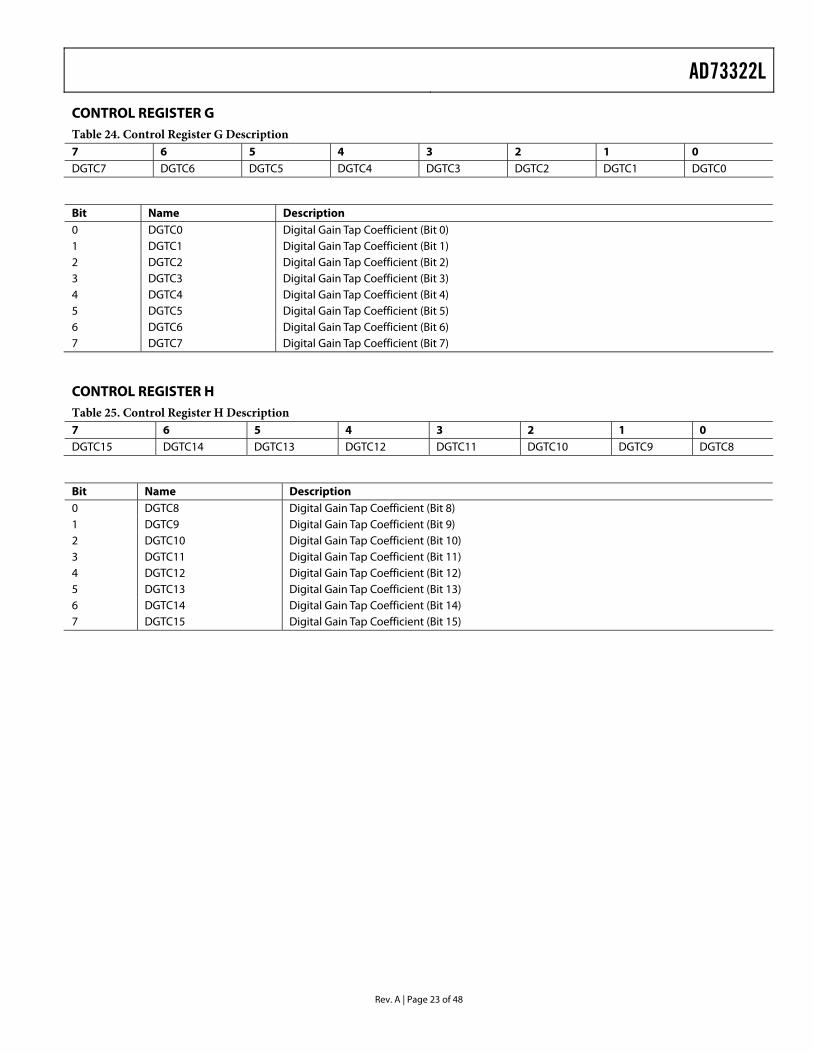
CONTROL REGISTER G Table 24. Control Register G Description 7 6 5 4 3 2 1 0 DGTC7 DGTC6 DGTC5 DGTC4 DGTC3 DGTC2 DGTC1 DGTC0
Bit Name Description 0 DGTC0 Digital Gain Tap Coefficient (Bit 0) 1 DGTC1 Digital Gain Tap Coefficient (Bit 1) 2 DGTC2 Digital Gain Tap Coefficient (Bit 2) 3 DGTC3 Digital Gain Tap Coefficient (Bit 3) 4 DGTC4 Digital Gain Tap Coefficient (Bit 4) 5 DGTC5 Digital Gain Tap Coefficient (Bit 5) 6 DGTC6 Digital Gain Tap Coefficient (Bit 6) 7 DGTC7 Digital Gain Tap Coefficient (Bit 7)
CONTROL REGISTER H Table 25. Control Register H Description 7 6 5 4 3 2 1 0 DGTC15 DGTC14 DGTC13 DGTC12 DGTC11 DGTC10 DGTC9 DGTC8
Bit Name Description 0 DGTC8 Digital Gain Tap Coefficient (Bit 8) 1 DGTC9 Digital Gain Tap Coefficient (Bit 9) 2 DGTC10 Digital Gain Tap Coefficient (Bit 10) 3 DGTC11 Digital Gain Tap Coefficient (Bit 11) 4 DGTC12 Digital Gain Tap Coefficient (Bit 12) 5 DGTC13 Digital Gain Tap Coefficient (Bit 13) 6 DGTC14 Digital Gain Tap Coefficient (Bit 14) 7 DGTC15 Digital Gain Tap Coefficient (Bit 15)
AD73322L
Rev. A | Page 24 of 48
OPERATION RESETTING THE AD73322L The RESET pin resets all the control registers. All registers are reset to zero, indicating that the default SCLK rate (DMCLK/8) and sample rate (DMCLK/2048) are at a minimum to ensure that slow speed DSP engines can communicate effectively. As well as resetting the control registers using the RESET pin, the device can be reset using the RESET bit (CRA:7) in Control Register A. Both hardware and software resets require four DMCLK cycles. On reset, DATA/PGM (CRA:0) is set to 0 (default condition) thus enabling program mode. The reset conditions ensure that the device must be programmed to the correct settings after power-up or reset. Following a reset, the SDOFS is asserted 2048 DMCLK cycles after RESET going high. The data that is output following reset and during program mode is random and contains no valid information until either data or mixed mode is set.
POWER MANAGEMENT The individual functional blocks of the AD73322L can be enabled separately by programming the Power Control Register CRC. It allows certain sections to be powered down if not required, which adds to the device’s flexibility in that the user need not incur the penalty of having to provide power for a certain section if it is not necessary to the design. The power control registers provide individual control settings for the major functional blocks on each codec unit and also a global override that allows all sections to be powered up by setting the bit. Using this method the user could, for example, individually enable a certain section, such as the reference (CRC:5), and disable all others. The global power-up (CRC:0) can be used to enable all sections, but if power-down is required using the global control, the reference is still enabled, in this case, because its individual bit is set. Refer to Table 21 for details of the settings of CRC.
NOTE: As both codec units share a common reference, the reference control bits (CRC:5-7) in each SPORT are wire-OR’ed to allow either device to control the reference.
OPERATING MODES There are three main modes of operation available on the AD73322L: program, data, and mixed program/data modes. Two other operating modes are typically reserved as diag- nostic modes: digital and SPORT loop-back. The device configuration—register settings—can be changed only in program and mixed program/data modes. In all modes, transfers of information to or from the device occur in 16-bit packets; therefore the DSP engine’s SPORT is programmed for 16-bit transfers.
PROGRAM (CONTROL) MODE In program mode, CRA:0 = 0, the user writes to the control registers to set up the device for desired operation—SPORT operation, cascade length, power management, input/output gain, etc. In this mode, the 16-bit information packet sent to the device by the DSP engine is interpreted as a control word whose format is shown in Table 17. In this mode, the user must address the device to be programmed using the address field of the control word. This field is read by the device and if it is zero (000 bin), the device recognizes the word as being addressed to it. If the address field is not zero, it is then decremented and the control word is passed out of the device—either to the next device in a cascade or back to the DSP engine.
This 3-bit address format allows the user to uniquely address any one of up to eight devices in a cascade; please note that this addressing scheme is valid only in sending control information to the device —a different format is used to send DAC data to the device(s). As the AD73322L is a dual codec, it features two separate device addresses for programming purposes. If the AD73322L is used in a standalone configuration connected to a DSP, the two device addresses correspond to 0 and 1. If the AD73322L is configured in a cascade of multiple, dual, or single codecs (AD73322L or AD73311), its device addresses correspond with its hardwired position in the cascade.
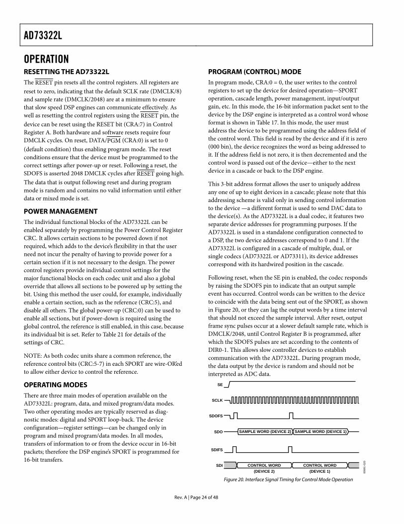
Following reset, when the SE pin is enabled, the codec responds by raising the SDOFS pin to indicate that an output sample event has occurred. Control words can be written to the device to coincide with the data being sent out of the SPORT, as shown in Figure 20, or they can lag the output words by a time interval that should not exceed the sample interval. After reset, output frame sync pulses occur at a slower default sample rate, which is DMCLK/2048, until Control Register B is programmed, after which the SDOFS pulses are set according to the contents of DIR0-1. This allows slow controller devices to establish communication with the AD73322L. During program mode, the data output by the device is random and should not be interpreted as ADC data.
SAMPLE WORD (DEVICE 2)
SE
SDOFS
SCLK
SDO
SDIFS
SDI
SAMPLE WORD (DEVICE 1)
CONTROL WORD(DEVICE 2)
CONTROL WORD(DEVICE 1) 00
691-
020
Figure 20. Interface Signal Timing for Control Mode Operation
AD73322L
Rev. A | Page 25 of 48
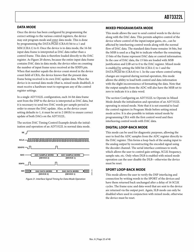
DATA MODE Once the device has been configured by programming the correct settings to the various control registers, the device may exit program mode and enter data mode. This is done by programming the DATA/PGM (CRA:0) bit to a 1 and MM (CRA:1) to 0. Once the device is in data mode, the 16-bit input data frame is interpreted as DAC data rather than a control frame. This data is therefore loaded directly to the DAC register. As Figure 20 shows, because the entire input data frame contains DAC data in data mode, the device relies on counting the number of input frame syncs received at the SDIFS pin. When that number equals the device count stored in the device count field of CRA, the device knows that the present data frame being received is its own DAC update data. When the device is in normal data mode (that is, mixed mode disabled), it must receive a hardware reset to reprogram any of the control register settings.
In a single AD73322L configuration, each 16-bit data frame sent from the DSP to the device is interpreted as DAC data, but it is necessary to send two DAC words per sample period in order to ensure the DAC update. Also, as the device count setting defaults to 1, it must be set to 2 (001b) to ensure correct update of both DACs on the AD73322L.
The section DAC Timing Control Example details the initial-ization and operation of an AD73322L in normal data mode.
SE
SDOFS
SCLK
SDO
SDIFS
SDI
ADC SAMPLE WORD(DEVICE 2)
ADC SAMPLE WORD(DEVICE 1)
DAC DATA WORD(DEVICE 2)
DAC DATA WORD(DEVICE 1) 00
691-
021
Figure 21. Interface Signal Timing for Data Mode Operation
MIXED PROGRAM/DATA MODE This mode allows the user to send control words to the device along with the DAC data. This permits adaptive control of the device where control of the input/output gains, etc., can be affected by interleaving control words along with the normal flow of DAC data. The standard data frame remains 16 bits, but the MSB is used as a flag bit to indicate whether the remaining 15 bits of the frame represent DAC data or control information. In the case of DAC data, the 15 bits are loaded with MSB justification and LSB set to 0 to the DAC register. Mixed mode is enabled by setting the MM bit (CRA:1) to 1 and the DATA/PGM bit (CRA:0) to 1. In the case where control setting changes are required during normal operation, this mode allows the ability to load both control and data information with the slight inconvenience of formatting the data. Note that the output samples from the ADC will also have the MSB set to zero to indicate it is a data-word.
The section Configuring an AD73322L to Operate in Mixed Mode details the initialization and operation of an AD73322L operating in mixed mode. Note that it is not essential to load the control registers in Program Mode before setting mixed mode active. It is also possible to initiate mixed mode by programming CRA with the first control word and then interleaving control words with DAC data.
DIGITAL LOOP-BACK MODE This mode can be used for diagnostic purposes, allowing the user to feed the ADC samples from the ADC register directly to the DAC register. This forms a loop-back of the analog input to the analog output by reconstructing the encoded signal using the decoder channel. The serial interface continues to work, which allows the user to control gain settings, SCLK frequency, sample rate, etc. Only when DLB is enabled with mixed mode operation can the user disable the DLB—otherwise the device must be reset.
SPORT LOOP-BACK MODE This mode allows the user to verify the DSP interfacing and connection by writing words to the SPORT of the devices and have them returned back unchanged after a delay of 16 SCLK cycles. The frame sync and data-word that are sent to the device are returned via the output port. Again, SLB mode can only be disabled when used in conjunction with mixed mode, otherwise the device must be reset.
AD73322L
Rev. A | Page 26 of 48
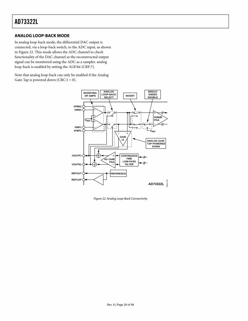
ANALOG LOOP-BACK MODE In analog loop-back mode, the differential DAC output is connected, via a loop-back switch, to the ADC input, as shown in Figure 22. This mode allows the ADC channel to check functionality of the DAC channel as the reconstructed output signal can be monitored using the ADC as a sampler. analog loop-back is enabled by setting the ALB bit (CRF:7).
Note that analog loop-back can only be enabled if the Analog Gain Tap is powered down (CRC:1 = 0).
0069
1-02
2
INVERTINGOP AMPS
ANALOG GAINTAP POWERED
DOWN
ANALOGLOOP-BACK
SELECT INVERTSINGLE-ENDED
ENABLE
CONTINUOUSTIME
LOW-PASSFILTER
VREF
VFBN1VINN1
VINP1VFBP1
VOUTP1
VOUTN1
AD73322L
+6/–15dBPGA
0/38dBPGA
GAIN±1
REFOUT
REFCAP
REFERENCE
VREF
Figure 22. Analog Loop-Back Connectivity
AD73322L
Rev. A | Page 27 of 48
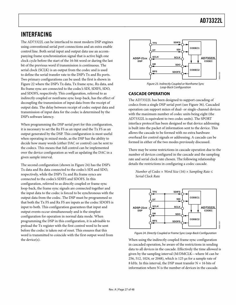
INTERFACING The AD73322L can be interfaced to most modern DSP engines using conventional serial port connections and an extra enable control line. Both serial input and output data use an accom-panying frame synchronization signal that is active high one clock cycle before the start of the 16-bit word or during the last bit of the previous word if transmission is continuous. The serial clock (SCLK) is an output from the codec and is used to define the serial transfer rate to the DSP’s Tx and Rx ports. Two primary configurations can be used: the first is shown in Figure 22 where the DSP’s Tx data, Tx frame sync, Rx data, and Rx frame sync are connected to the codec’s SDI, SDIFS, SDO, and SDOFS, respectively. This configuration, referred to as indirectly coupled or nonframe sync loop-back, has the effect of decoupling the transmission of input data from the receipt of output data. The delay between receipt of codec output data and transmission of input data for the codec is determined by the DSP’s software latency.
When programming the DSP serial port for this configuration, it is necessary to set the Rx FS as an input and the Tx FS as an output generated by the DSP. This configuration is most useful when operating in mixed mode, as the DSP has the ability to decide how many words (either DAC or control) can be sent to the codecs. This means that full control can be implemented over the device configuration as well as updating the DAC in a given sample interval.
The second configuration (shown in Figure 24) has the DSP’s Tx data and Rx data connected to the codec’s SDI and SDO, respectively, while the DSP’s Tx and Rx frame syncs are connected to the codec’s SDIFS and SDOFS. In this configuration, referred to as directly coupled or frame sync loop-back, the frame sync signals are connected together and the input data to the codec is forced to be synchronous with the output data from the codec. The DSP must be programmed so that both the Tx FS and Rx FS are inputs as the codec SDOFS is input to both. This configuration guarantees that input and output events occur simultaneously and is the simplest configuration for operation in normal data mode. When programming the DSP in this configuration, it is advisable to preload the Tx register with the first control word to be sent before the codec is taken out of reset. This ensures that this word is transmitted to coincide with the first output word from the device(s).
TFS
DT
SCLK
DR
RFS
ADSP-21xxDSP
AD73322LCODEC
CODEC1
CODEC2
SDIFS
SDI
SCLK
SDO
SDOFS
0069
1-02
3
Figure 23. Indirectly Coupled or Nonframe Sync Loop-Back Configuration
CASCADE OPERATION The AD73322L has been designed to support cascading of codecs from a single DSP serial port (see Figure 36). Cascaded operation can support mixes of dual- or single-channel devices with the maximum number of codec units being eight (the AD73322L is equivalent to two codec units). The SPORT interface protocol has been designed so that device addressing is built into the packet of information sent to the device. This allows the cascade to be formed with no extra hardware overhead for control signals or addressing. A cascade can be formed in either of the two modes previously discussed.
There may be some restrictions in cascade operation due to the number of devices configured in the cascade and the sampling rate and serial clock rate chosen. The following relationship details the restrictions in configuring a codec cascade.
Number of Codes × Word Size (16) × Sampling Rate ≤ Serial Clock Rate
0069
1-02
4
TFS
DT
SCLK
DR
RFS
ADSP-21xxDSP
AD73322LCODEC
CODEC1
CODEC2
SDIFS
SDI
SCLK
SDO
SDOFS
Figure 24. Directly Coupled or Frame Sync Loop-Back Configuration
When using the indirectly coupled frame sync configuration in cascaded operation, be aware of the restrictions in sending data to all devices in the cascade. Effectively the time allowed is given by the sampling interval (M/DMCLK—where M can be 256, 512, 1024, or 2048), which is 125 µs for a sample rate of 8 kHz. In this interval, the DSP must transfer N × 16 bits of information where N is the number of devices in the cascade.
AD73322L
Rev. A | Page 28 of 48
Each bit will take 1/SCLK and, allowing for any latency between the receipt of the Rx interrupt and the transmission of the Tx data, the relationship for successful operation is given by
M/DMCLK > ((N × 16/SCLK) + TINTERRUPT LATENCY)
The interrupt latency will include the time between the ADC sampling event and the Rx interrupt being generated in the DSP—this should be 16 SCLK cycles.
Because the AD73322L is configured in cascade mode, each device must know the number of devices in the cascade because the data and mixed modes use a method of counting input frame sync pulses to decide when they should update the DAC register from the serial input register. Control Register A contains a 3-bit field (DC0-2) that is programmed by the DSP during the programming phase. The default condition is that the field contains 000b, which is equivalent to a single device in the cascade (see Table 26). However, for cascade operation this field must contain a binary value that is one less than the number of devices in the cascade, which is 001b for a single AD73322L device configuration.
Table 26. Device Count Settings DC2 DC1 DC0 Cascade Length 0 0 0 1 0 0 1 2 0 0 3 0 1 1 4 1 0 0 5 1 0 1 6 1 1 0 7 1 1 1 8
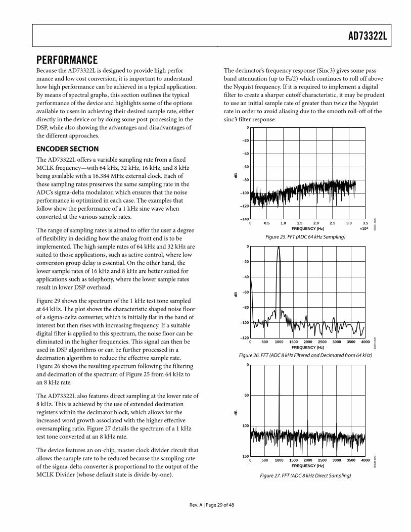
AD73322L
Rev. A | Page 29 of 48
PERFORMANCE Because the AD73322L is designed to provide high perfor-mance and low cost conversion, it is important to understand how high performance can be achieved in a typical application. By means of spectral graphs, this section outlines the typical performance of the device and highlights some of the options available to users in achieving their desired sample rate, either directly in the device or by doing some post-processing in the DSP, while also showing the advantages and disadvantages of the different approaches.
ENCODER SECTION The AD73322L offers a variable sampling rate from a fixed MCLK frequency—with 64 kHz, 32 kHz, 16 kHz, and 8 kHz being available with a 16.384 MHz external clock. Each of these sampling rates preserves the same sampling rate in the ADC’s sigma-delta modulator, which ensures that the noise performance is optimized in each case. The examples that follow show the performance of a 1 kHz sine wave when converted at the various sample rates.
The range of sampling rates is aimed to offer the user a degree of flexibility in deciding how the analog front end is to be implemented. The high sample rates of 64 kHz and 32 kHz are suited to those applications, such as active control, where low conversion group delay is essential. On the other hand, the lower sample rates of 16 kHz and 8 kHz are better suited for applications such as telephony, where the lower sample rates result in lower DSP overhead.
Figure 29 shows the spectrum of the 1 kHz test tone sampled at 64 kHz. The plot shows the characteristic shaped noise floor of a sigma-delta converter, which is initially flat in the band of interest but then rises with increasing frequency. If a suitable digital filter is applied to this spectrum, the noise floor can be eliminated in the higher frequencies. This signal can then be used in DSP algorithms or can be further processed in a decimation algorithm to reduce the effective sample rate. Figure 26 shows the resulting spectrum following the filtering and decimation of the spectrum of Figure 25 from 64 kHz to an 8 kHz rate.
The AD73322L also features direct sampling at the lower rate of 8 kHz. This is achieved by the use of extended decimation registers within the decimator block, which allows for the increased word growth associated with the higher effective oversampling ratio. Figure 27 details the spectrum of a 1 kHz test tone converted at an 8 kHz rate.
The device features an on-chip, master clock divider circuit that allows the sample rate to be reduced because the sampling rate of the sigma-delta converter is proportional to the output of the MCLK Divider (whose default state is divide-by-one).
The decimator’s frequency response (Sinc3) gives some pass-band attenuation (up to FS/2) which continues to roll off above the Nyquist frequency. If it is required to implement a digital filter to create a sharper cutoff characteristic, it may be prudent to use an initial sample rate of greater than twice the Nyquist rate in order to avoid aliasing due to the smooth roll-off of the sinc3 filter response.
0069
1-02
5
FREQUENCY (Hz) ×1043.50 0.5 1.0 1.5 2.0 2.5 3.0
dB
0
–40
–20
–60
–80
–100
–120
–140
Figure 25. FFT (ADC 64 kHz Sampling)
0069
1-02
6
FREQUENCY (Hz)40000 500 1000 1500 2000 2500 3000 3500
dB
0
–20
–40
–60
–80
–100
–120
Figure 26. FFT (ADC 8 kHz Filtered and Decimated from 64 kHz)
0069
1-02
7
FREQUENCY (Hz)40000 500 1000 1500 2000 2500 3000 3500
dB
0
50
100
150
Figure 27. FFT (ADC 8 kHz Direct Sampling)
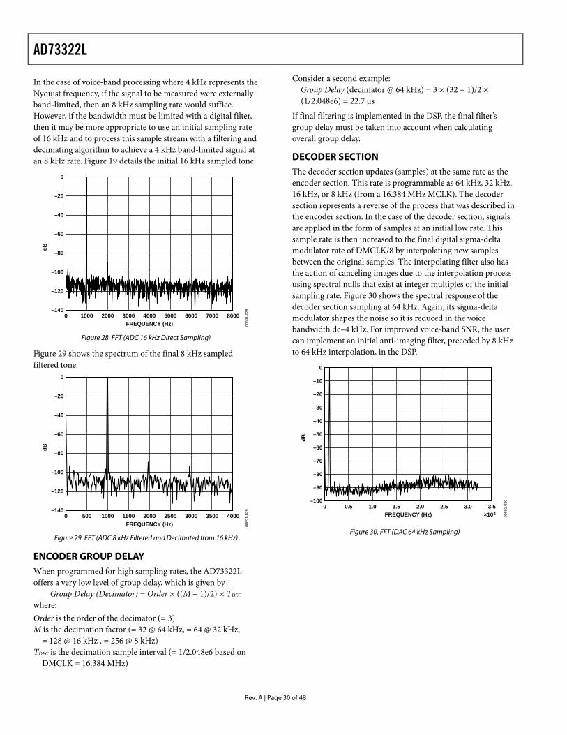
AD73322L
Rev. A | Page 30 of 48
In the case of voice-band processing where 4 kHz represents the Nyquist frequency, if the signal to be measured were externally band-limited, then an 8 kHz sampling rate would suffice. However, if the bandwidth must be limited with a digital filter, then it may be more appropriate to use an initial sampling rate of 16 kHz and to process this sample stream with a filtering and decimating algorithm to achieve a 4 kHz band-limited signal at an 8 kHz rate. Figure 19 details the initial 16 kHz sampled tone.
0069
1-02
8
FREQUENCY (Hz)80000 1000 2000 3000 4000 5000 6000 7000
dB
0
–40
–20
–60
–80
–100
–120
–140
Figure 28. FFT (ADC 16 kHz Direct Sampling)
Figure 29 shows the spectrum of the final 8 kHz sampled filtered tone.
0069
1-02
9
FREQUENCY (Hz)40002500 3000 35000 500 1000 1500 2000
dB
0
–20
–40
–60
–80
–100
–120
–140
Figure 29. FFT (ADC 8 kHz Filtered and Decimated from 16 kHz)
ENCODER GROUP DELAY When programmed for high sampling rates, the AD73322L offers a very low level of group delay, which is given by
Group Delay (Decimator) = Order × ((M − 1)/2) × TDEC
where: Order is the order of the decimator (= 3) M is the decimation factor (= 32 @ 64 kHz, = 64 @ 32 kHz,
= 128 @ 16 kHz , = 256 @ 8 kHz) TDEC is the decimation sample interval (= 1/2.048e6 based on
DMCLK = 16.384 MHz)
Consider a second example: Group Delay (decimator @ 64 kHz) = 3 × (32 − 1)/2 × (1/2.048e6) = 22.7 µs
If final filtering is implemented in the DSP, the final filter’s group delay must be taken into account when calculating overall group delay.
DECODER SECTION The decoder section updates (samples) at the same rate as the encoder section. This rate is programmable as 64 kHz, 32 kHz, 16 kHz, or 8 kHz (from a 16.384 MHz MCLK). The decoder section represents a reverse of the process that was described in the encoder section. In the case of the decoder section, signals are applied in the form of samples at an initial low rate. This sample rate is then increased to the final digital sigma-delta modulator rate of DMCLK/8 by interpolating new samples between the original samples. The interpolating filter also has the action of canceling images due to the interpolation process using spectral nulls that exist at integer multiples of the initial sampling rate. Figure 30 shows the spectral response of the decoder section sampling at 64 kHz. Again, its sigma-delta modulator shapes the noise so it is reduced in the voice bandwidth dc–4 kHz. For improved voice-band SNR, the user can implement an initial anti-imaging filter, preceded by 8 kHz to 64 kHz interpolation, in the DSP.
0069
1-03
0
FREQUENCY (Hz) ×1043.50 0.5 1.0 1.5 2.0 2.5 3.0
dB
0
–20
–10
–40
–30
–60
–50
–80
–70
–90
–100
Figure 30. FFT (DAC 64 kHz Sampling)
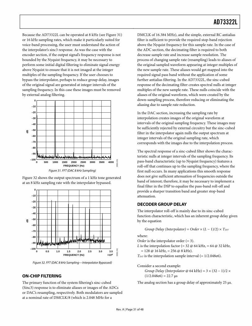
AD73322L
Rev. A | Page 31 of 48
Because the AD73322L can be operated at 8 kHz (see Figure 31) or 16 kHz sampling rates, which make it particularly suited for voice-band processing, the user must understand the action of the interpolator’s sinc3 response. As was the case with the encoder section, if the output signal’s frequency response is not bounded by the Nyquist frequency, it may be necessary to perform some initial digital filtering to eliminate signal energy above Nyquist to ensure that it is not imaged at the integer multiples of the sampling frequency. If the user chooses to bypass the interpolator, perhaps to reduce group delay, images of the original signal are generated at integer intervals of the sampling frequency. In this case these images must be removed by external analog filtering.
0069
1-03
1
FREQUENCY (Hz)40000 500 1000 1500 2000 2500 3000 3500
dB
0
–10
–20
–30
–40
–50
–60
–70
–80
–90
–100
Figure 31. FFT (DAC 8 kHz Sampling)
Figure 32 shows the output spectrum of a 1 kHz tone generated at an 8 kHz sampling rate with the interpolator bypassed.
0069
1-03
2
FREQUENCY (Hz) ×1043.50 0.5 1.0 1.5 2.0 2.5 3.0
dB
0
–10
–30
–20
–40
–50
–70
–60
–90
–80
–100
Figure 32. FFT (DAC 8 kHz Sampling—Interpolator Bypassed)
ON-CHIP FILTERING The primary function of the system filtering’s sinc-cubed (Sinc3) response is to eliminate aliases or images of the ADCs or DAC’s resampling, respectively. Both modulators are sampled at a nominal rate of DMCLK/8 (which is 2.048 MHz for a
DMCLK of 16.384 MHz), and the simple, external RC antialias filter is sufficient to provide the required stop-band rejection above the Nyquist frequency for this sample rate. In the case of the ADC section, the decimating filter is required to both decrease sample rate and increase sample resolution. The process of changing sample rate (resampling) leads to aliases of the original sampled waveform appearing at integer multiples of the new sample rate. These aliases would get mapped into the required signal pass band without the application of some further antialias filtering. In the AD73322L, the sinc-cubed response of the decimating filter creates spectral nulls at integer multiples of the new sample rate. These nulls coincide with the aliases of the original waveform, which were created by the down-sampling process, therefore reducing or eliminating the aliasing due to sample rate reduction.
In the DAC section, increasing the sampling rate by interpolation creates images of the original waveform at intervals of the original sampling frequency. These images may be sufficiently rejected by external circuitry but the sinc-cubed filter in the interpolator again nulls the output spectrum at integer intervals of the original sampling rate, which corresponds with the images due to the interpolation process.
The spectral response of a sinc-cubed filter shows the charac-teristic nulls at integer intervals of the sampling frequency. Its pass-band characteristic (up to Nyquist frequency) features a roll-off that continues up to the sampling frequency, where the first null occurs. In many applications this smooth response does not give sufficient attenuation of frequencies outside the band of interest; therefore, it may be necessary to implement a final filter in the DSP to equalize the pass-band roll-off and provide a sharper transition band and greater stop-band attenuation.
DECODER GROUP DELAY The interpolator roll-off is mainly due to its sinc-cubed function characteristic, which has an inherent group delay given by the equation
Group Delay (Interpolator) = Order × (L − 1)/2) × TINT
where: Order is the interpolator order (= 3). L is the interpolation factor (= 32 @ 64 kHz, = 64 @ 32 kHz,
= 128 @ 16 kHz, = 256 @ 8 kHz). TINT is the interpolation sample interval (= 1/2.048e6). Consider a second example:
Group Delay (Interpolator @ 64 kHz) = 3 × (32 − 1)/2 × (1/2.048e6) = 22.7 µs
The analog section has a group delay of approximately 25 µs.
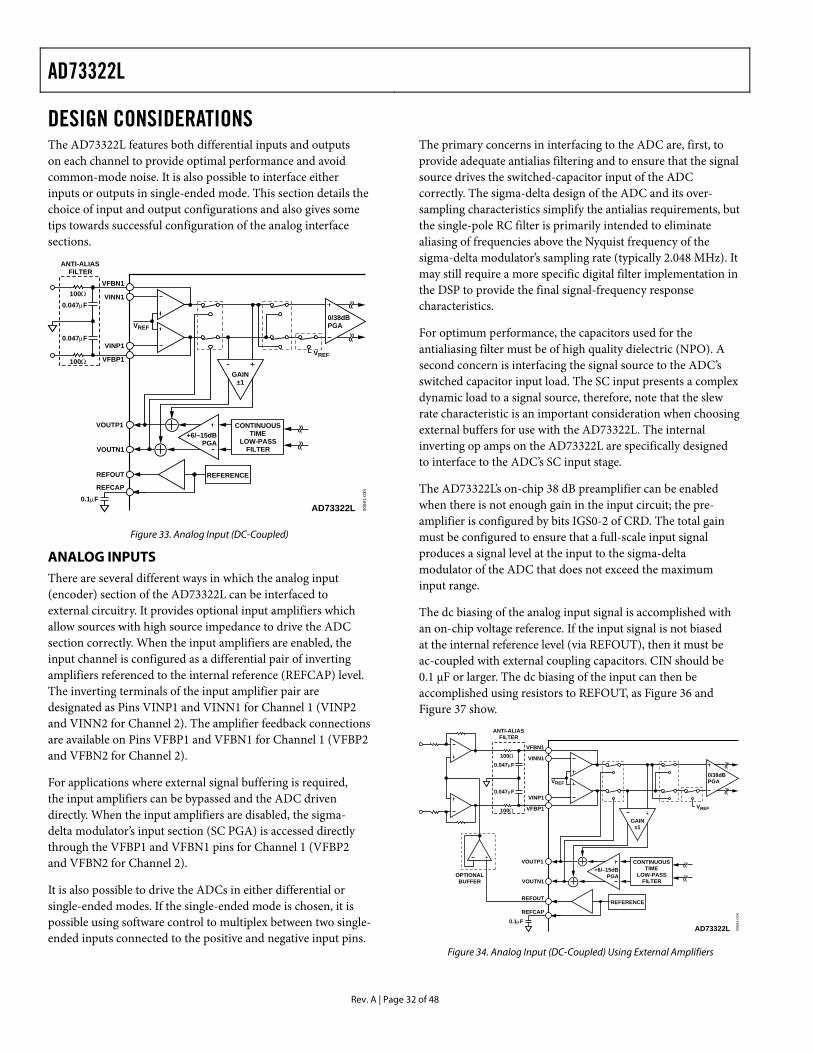
AD73322L
Rev. A | Page 32 of 48
DESIGN CONSIDERATIONS The AD73322L features both differential inputs and outputs on each channel to provide optimal performance and avoid common-mode noise. It is also possible to interface either inputs or outputs in single-ended mode. This section details the choice of input and output configurations and also gives some tips towards successful configuration of the analog interface sections.
CONTINUOUSTIME
LOW-PASSFILTER
VREF
VFBN1
VINN1
VINP1
VFBP1
VOUTP1
VOUTN1
AD73322L
+6/–15dBPGA
0/38dBPGA
GAIN±1
REFOUT
REFCAP
REFERENCE
VREF00
691-
033
0.047µF
0.047µF
100Ω
100Ω
0.1µF
ANTI-ALIASFILTER
Figure 33. Analog Input (DC-Coupled)
ANALOG INPUTS There are several different ways in which the analog input (encoder) section of the AD73322L can be interfaced to external circuitry. It provides optional input amplifiers which allow sources with high source impedance to drive the ADC section correctly. When the input amplifiers are enabled, the input channel is configured as a differential pair of inverting amplifiers referenced to the internal reference (REFCAP) level. The inverting terminals of the input amplifier pair are designated as Pins VINP1 and VINN1 for Channel 1 (VINP2 and VINN2 for Channel 2). The amplifier feedback connections are available on Pins VFBP1 and VFBN1 for Channel 1 (VFBP2 and VFBN2 for Channel 2).
For applications where external signal buffering is required, the input amplifiers can be bypassed and the ADC driven directly. When the input amplifiers are disabled, the sigma- delta modulator’s input section (SC PGA) is accessed directly through the VFBP1 and VFBN1 pins for Channel 1 (VFBP2 and VFBN2 for Channel 2).
It is also possible to drive the ADCs in either differential or single-ended modes. If the single-ended mode is chosen, it is possible using software control to multiplex between two single-ended inputs connected to the positive and negative input pins.
The primary concerns in interfacing to the ADC are, first, to provide adequate antialias filtering and to ensure that the signal source drives the switched-capacitor input of the ADC correctly. The sigma-delta design of the ADC and its over-sampling characteristics simplify the antialias requirements, but the single-pole RC filter is primarily intended to eliminate aliasing of frequencies above the Nyquist frequency of the sigma-delta modulator’s sampling rate (typically 2.048 MHz). It may still require a more specific digital filter implementation in the DSP to provide the final signal-frequency response characteristics.
For optimum performance, the capacitors used for the antialiasing filter must be of high quality dielectric (NPO). A second concern is interfacing the signal source to the ADC’s switched capacitor input load. The SC input presents a complex dynamic load to a signal source, therefore, note that the slew rate characteristic is an important consideration when choosing external buffers for use with the AD73322L. The internal inverting op amps on the AD73322L are specifically designed to interface to the ADC’s SC input stage.
The AD73322L’s on-chip 38 dB preamplifier can be enabled when there is not enough gain in the input circuit; the pre-amplifier is configured by bits IGS0-2 of CRD. The total gain must be configured to ensure that a full-scale input signal produces a signal level at the input to the sigma-delta modulator of the ADC that does not exceed the maximum input range.
The dc biasing of the analog input signal is accomplished with an on-chip voltage reference. If the input signal is not biased at the internal reference level (via REFOUT), then it must be ac-coupled with external coupling capacitors. CIN should be 0.1 µF or larger. The dc biasing of the input can then be accomplished using resistors to REFOUT, as Figure 36 and Figure 37 show.
CONTINUOUSTIME
LOW-PASSFILTER
VREF
VFBN1
VINN1
VINP1
VFBP1
VOUTP1
VOUTN1
AD73322L
+6/–15dBPGA
0/38dBPGA
GAIN±1
REFOUT
REFCAP
REFERENCE
VREF
0.047µF
0.047µF
100Ω
100Ω
0.1µF
0069
1-03
4
OPTIONALBUFFER
ANTI-ALIASFILTER
Figure 34. Analog Input (DC-Coupled) Using External Amplifiers
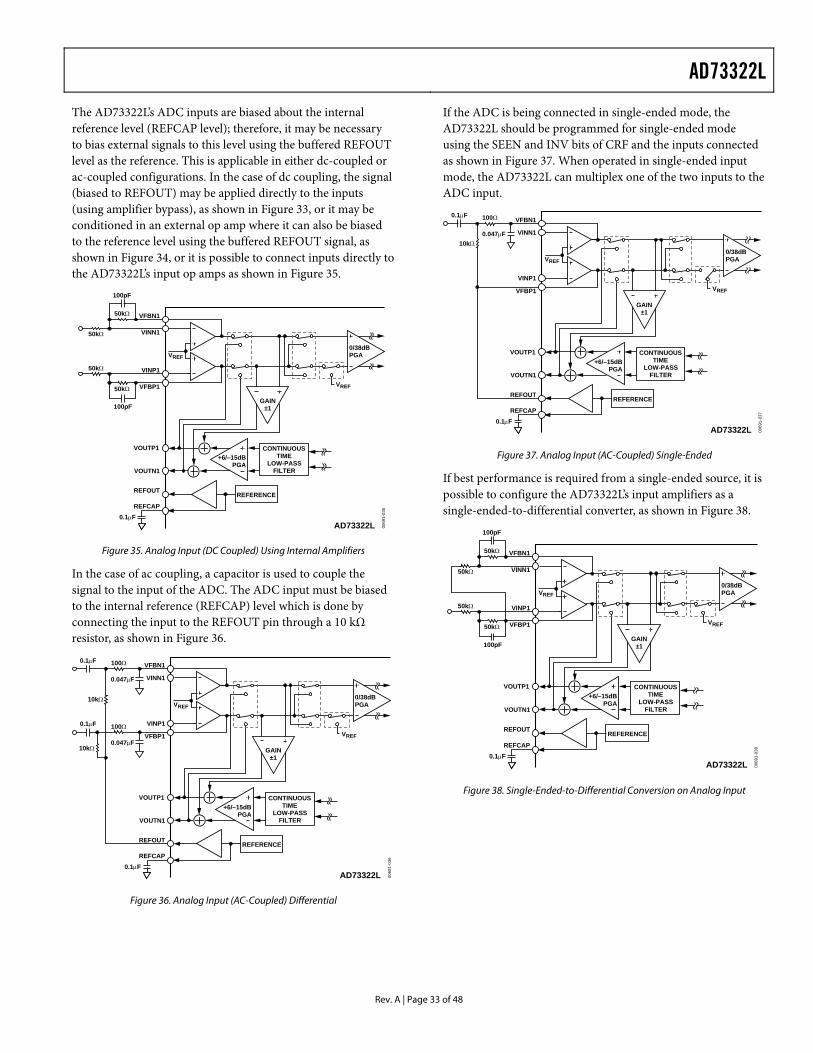
AD73322L
Rev. A | Page 33 of 48
The AD73322L’s ADC inputs are biased about the internal reference level (REFCAP level); therefore, it may be necessary to bias external signals to this level using the buffered REFOUT level as the reference. This is applicable in either dc-coupled or ac-coupled configurations. In the case of dc coupling, the signal (biased to REFOUT) may be applied directly to the inputs (using amplifier bypass), as shown in Figure 33, or it may be conditioned in an external op amp where it can also be biased to the reference level using the buffered REFOUT signal, as shown in Figure 34, or it is possible to connect inputs directly to the AD73322L’s input op amps as shown in Figure 35.
CONTINUOUSTIME
LOW-PASSFILTER
VREF
VFBN1
VINN1
VINP1
VFBP1
VOUTP1
VOUTN1
AD73322L
+6/–15dBPGA
0/38dBPGA
GAIN±1
REFOUT
REFCAP
REFERENCE
VREF50kΩ
50kΩ
50kΩ
50kΩ
0.1µF
0069
1-03
5
100pF
100pF
Figure 35. Analog Input (DC Coupled) Using Internal Amplifiers
In the case of ac coupling, a capacitor is used to couple the signal to the input of the ADC. The ADC input must be biased to the internal reference (REFCAP) level which is done by connecting the input to the REFOUT pin through a 10 kΩ resistor, as shown in Figure 36.
CONTINUOUSTIME
LOW-PASSFILTER
VREF
VFBN1
VINN1
VINP1
VFBP1
VOUTP1
VOUTN1
AD73322L
+6/–15dBPGA
0/38dBPGA
GAIN±1
REFOUT
REFCAP
REFERENCE
VREF100Ω
100Ω
0.1µF
0.1µF
0.1µF
0069
1-03
6
0.047µF
0.047µF10kΩ
10kΩ
Figure 36. Analog Input (AC-Coupled) Differential
If the ADC is being connected in single-ended mode, the AD73322L should be programmed for single-ended mode using the SEEN and INV bits of CRF and the inputs connected as shown in Figure 37. When operated in single-ended input mode, the AD73322L can multiplex one of the two inputs to the ADC input.
CONTINUOUSTIME
LOW-PASSFILTER
VREF
VFBN1
VINN1
VINP1
VFBP1
VOUTP1
VOUTN1
AD73322L
+6/–15dBPGA
0/38dBPGA
GAIN±1
REFOUT
REFCAP
REFERENCE
VREF
100Ω
0.1µF
0.1µF
0.047µF10kΩ
0069
1-03
7
Figure 37. Analog Input (AC-Coupled) Single-Ended
If best performance is required from a single-ended source, it is possible to configure the AD73322L’s input amplifiers as a single-ended-to-differential converter, as shown in Figure 38.
CONTINUOUSTIME
LOW-PASSFILTER
VREF
VFBN1
VINN1
VINP1
VFBP1
VOUTP1
VOUTN1
AD73322L
+6/–15dBPGA
0/38dBPGA
GAIN±1
REFOUT
REFCAP
REFERENCE
VREF50kΩ
50kΩ
50kΩ
50kΩ
0.1µF
100pF
100pF
0069
1-03
8
Figure 38. Single-Ended-to-Differential Conversion on Analog Input
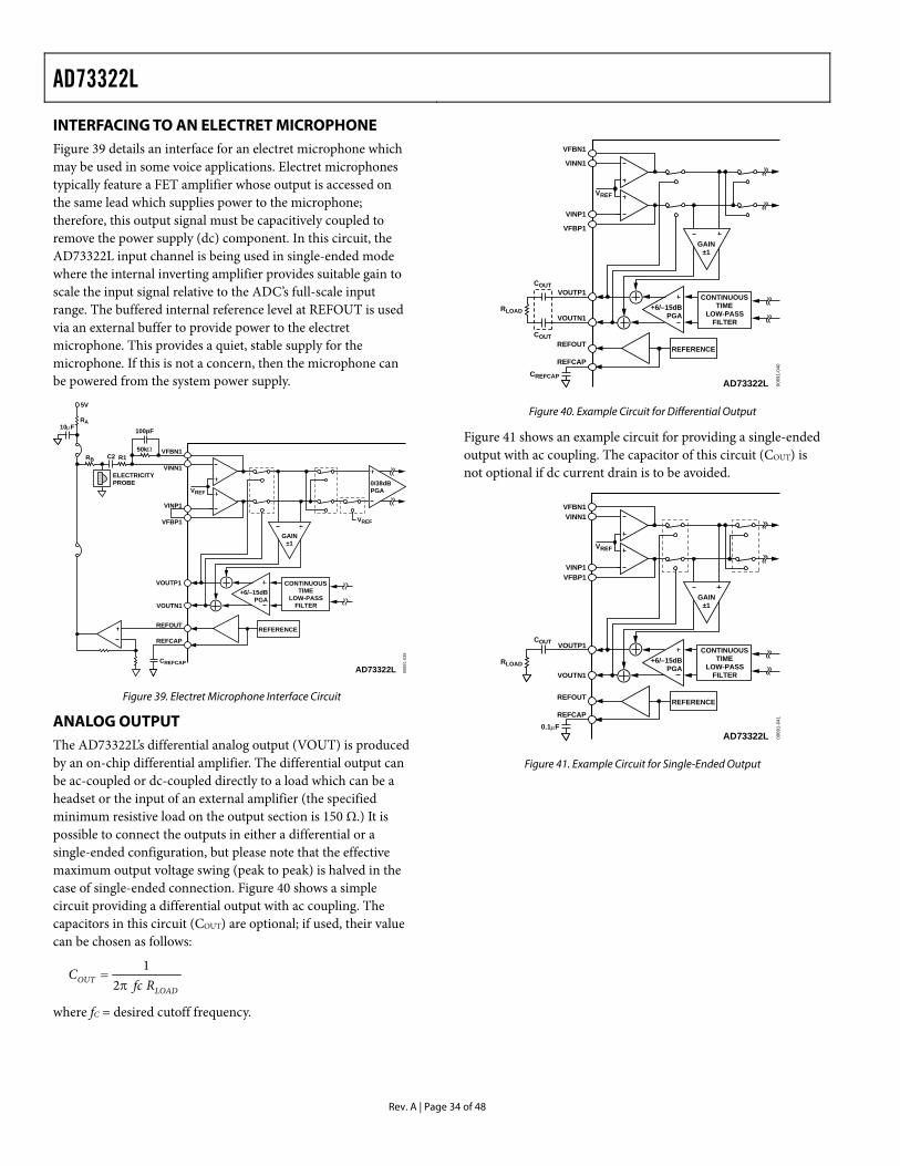
AD73322L
Rev. A | Page 34 of 48
INTERFACING TO AN ELECTRET MICROPHONE Figure 39 details an interface for an electret microphone which may be used in some voice applications. Electret microphones typically feature a FET amplifier whose output is accessed on the same lead which supplies power to the microphone; therefore, this output signal must be capacitively coupled to remove the power supply (dc) component. In this circuit, the AD73322L input channel is being used in single-ended mode where the internal inverting amplifier provides suitable gain to scale the input signal relative to the ADC’s full-scale input range. The buffered internal reference level at REFOUT is used via an external buffer to provide power to the electret microphone. This provides a quiet, stable supply for the microphone. If this is not a concern, then the microphone can be powered from the system power supply.
CONTINUOUSTIME
LOW-PASSFILTER
VREF
VFBN1
VINN1
VINP1
VFBP1
VOUTP1
VOUTN1
AD73322L
+6/–15dBPGA
0/38dBPGA
GAIN±1
REFOUT
REFCAP
REFERENCE
VREF
R1RB
RA
50kΩ
CREFCAP
100pF
C2
ELECTRICITYPROBE
10µF
5V00
691-
039
Figure 39. Electret Microphone Interface Circuit
ANALOG OUTPUT The AD73322L’s differential analog output (VOUT) is produced by an on-chip differential amplifier. The differential output can be ac-coupled or dc-coupled directly to a load which can be a headset or the input of an external amplifier (the specified minimum resistive load on the output section is 150 Ω.) It is possible to connect the outputs in either a differential or a single-ended configuration, but please note that the effective maximum output voltage swing (peak to peak) is halved in the case of single-ended connection. Figure 40 shows a simple circuit providing a differential output with ac coupling. The capacitors in this circuit (COUT) are optional; if used, their value can be chosen as follows:
LOADOUT Rfc
Cπ
=2
1
where fC = desired cutoff frequency.
CONTINUOUSTIME
LOW-PASSFILTER
VREF
VFBN1
VINN1
VINP1
VFBP1
VOUTP1
VOUTN1
AD73322L
+6/–15dBPGA
GAIN±1
REFOUT
REFCAP
REFERENCE
CREFCAP
RLOAD
COUT
COUT
0069
1-04
0
Figure 40. Example Circuit for Differential Output
Figure 41 shows an example circuit for providing a single-ended output with ac coupling. The capacitor of this circuit (COUT) is not optional if dc current drain is to be avoided.
0069
1-04
1
CONTINUOUSTIME
LOW-PASSFILTER
VREF
VFBN1VINN1
VINP1VFBP1
VOUTP1
VOUTN1
AD73322L
+6/–15dBPGA
GAIN±1
REFOUT
REFCAP
REFERENCE
0.1µF
RLOAD
COUT
Figure 41. Example Circuit for Single-Ended Output
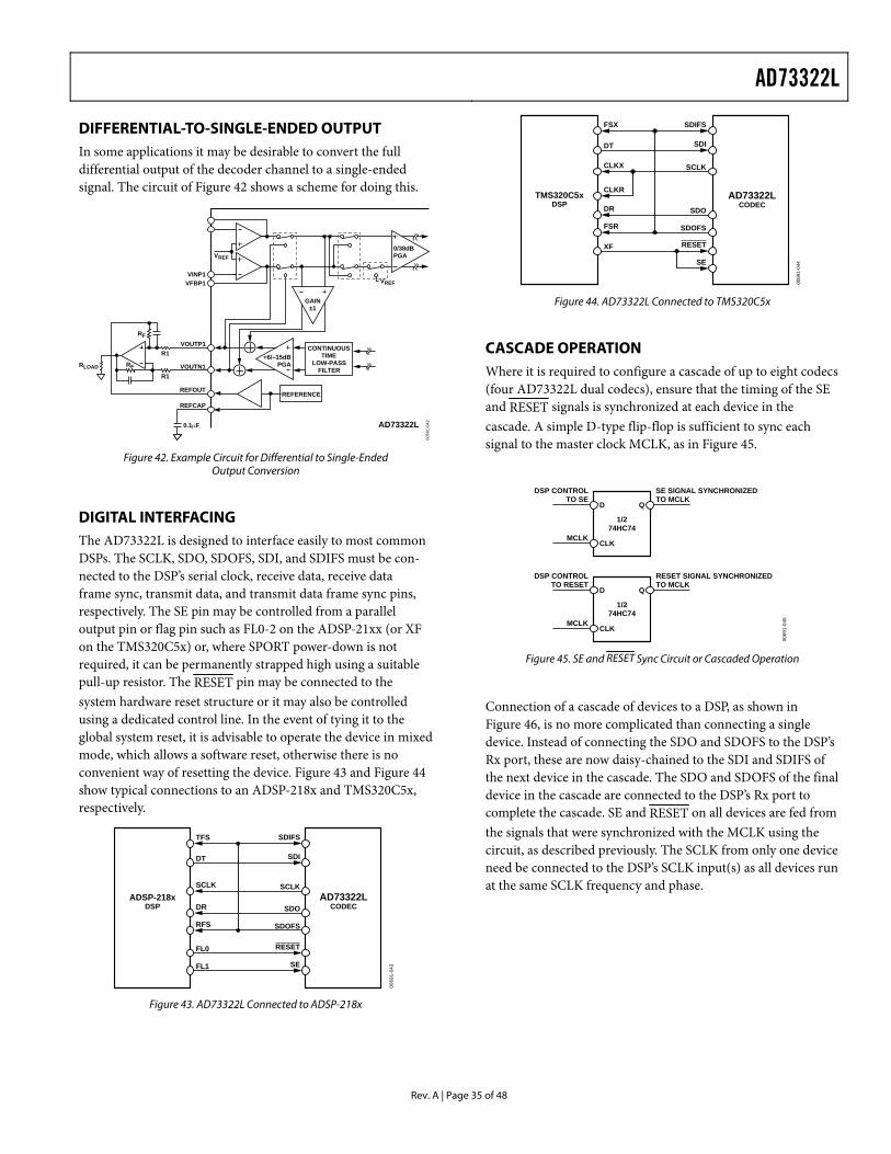
AD73322L
Rev. A | Page 35 of 48
DIFFERENTIAL-TO-SINGLE-ENDED OUTPUT In some applications it may be desirable to convert the full differential output of the decoder channel to a single-ended signal. The circuit of Figure 42 shows a scheme for doing this.
CONTINUOUSTIME
LOW-PASSFILTER
VREF
VINP1VFBP1
VOUTP1
VOUTN1
AD73322L
+6/–15dBPGA
0/38dBPGA
GAIN±1
REFOUT
REFCAP
REFERENCE
VREF
0.1µF00
691-
042
RF
R1
R1
RF
RLOAD
Figure 42. Example Circuit for Differential to Single-Ended
Output Conversion
DIGITAL INTERFACING The AD73322L is designed to interface easily to most common DSPs. The SCLK, SDO, SDOFS, SDI, and SDIFS must be con-nected to the DSP’s serial clock, receive data, receive data frame sync, transmit data, and transmit data frame sync pins, respectively. The SE pin may be controlled from a parallel output pin or flag pin such as FL0-2 on the ADSP-21xx (or XF on the TMS320C5x) or, where SPORT power-down is not required, it can be permanently strapped high using a suitable pull-up resistor. The RESET pin may be connected to the system hardware reset structure or it may also be controlled using a dedicated control line. In the event of tying it to the global system reset, it is advisable to operate the device in mixed mode, which allows a software reset, otherwise there is no convenient way of resetting the device. Figure 43 and Figure 44 show typical connections to an ADSP-218x and TMS320C5x, respectively.
TFS
DT
SCLK
DR
RFS
ADSP-218xDSP
AD73322LCODEC
SDIFS
SDI
SCLK
SDO
SDOFS
FL0
FL1
RESET
SE
0069
1-04
3
Figure 43. AD73322L Connected to ADSP-218x
FSX
DT
CLKX
DR
FSR
TMS320C5xDSP
AD73322LCODEC
SDIFS
SDI
SCLK
SDO
SDOFS
XF RESET
SE
CLKR
0069
1-04
4
Figure 44. AD73322L Connected to TMS320C5x
CASCADE OPERATION Where it is required to configure a cascade of up to eight codecs (four AD73322L dual codecs), ensure that the timing of the SE and RESET signals is synchronized at each device in the cascade. A simple D-type flip-flop is sufficient to sync each signal to the master clock MCLK, as in Figure 45.
1/274HC74
CLK
D Q
DSP CONTROLTO SE
MCLK
SE SIGNAL SYNCHRONIZEDTO MCLK
1/274HC74
CLK
D Q
DSP CONTROLTO RESET
MCLK
RESET SIGNAL SYNCHRONIZEDTO MCLK
0069
1-04
5
Figure 45. SE and RESET Sync Circuit or Cascaded Operation
Connection of a cascade of devices to a DSP, as shown in Figure 46, is no more complicated than connecting a single device. Instead of connecting the SDO and SDOFS to the DSP’s Rx port, these are now daisy-chained to the SDI and SDIFS of the next device in the cascade. The SDO and SDOFS of the final device in the cascade are connected to the DSP’s Rx port to complete the cascade. SE and RESET on all devices are fed from the signals that were synchronized with the MCLK using the circuit, as described previously. The SCLK from only one device need be connected to the DSP’s SCLK input(s) as all devices run at the same SCLK frequency and phase.
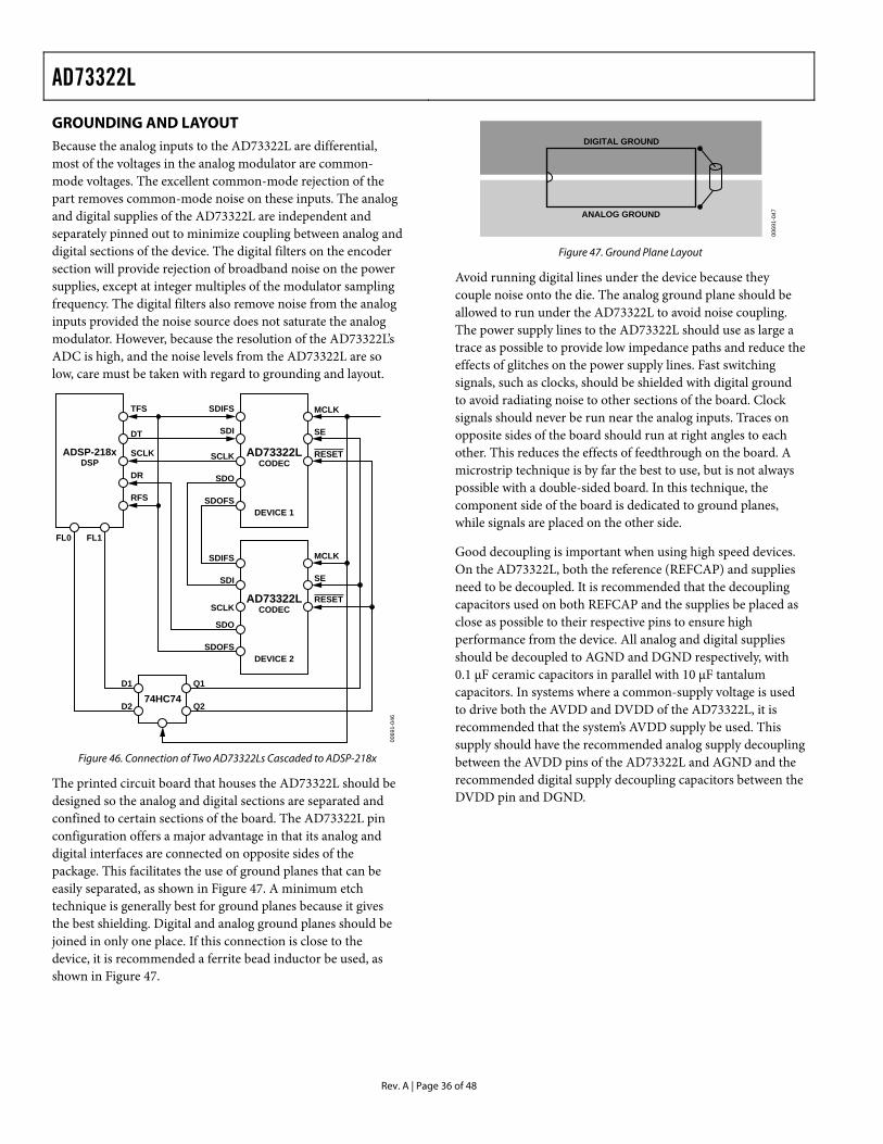
AD73322L
Rev. A | Page 36 of 48
GROUNDING AND LAYOUT DIGITAL GROUND
ANALOG GROUND
0069
1-04
7
Because the analog inputs to the AD73322L are differential, most of the voltages in the analog modulator are common-mode voltages. The excellent common-mode rejection of the part removes common-mode noise on these inputs. The analog and digital supplies of the AD73322L are independent and separately pinned out to minimize coupling between analog and digital sections of the device. The digital filters on the encoder section will provide rejection of broadband noise on the power supplies, except at integer multiples of the modulator sampling frequency. The digital filters also remove noise from the analog inputs provided the noise source does not saturate the analog modulator. However, because the resolution of the AD73322L’s ADC is high, and the noise levels from the AD73322L are so low, care must be taken with regard to grounding and layout.
Figure 47. Ground Plane Layout
Avoid running digital lines under the device because they couple noise onto the die. The analog ground plane should be allowed to run under the AD73322L to avoid noise coupling. The power supply lines to the AD73322L should use as large a trace as possible to provide low impedance paths and reduce the effects of glitches on the power supply lines. Fast switching signals, such as clocks, should be shielded with digital ground to avoid radiating noise to other sections of the board. Clock signals should never be run near the analog inputs. Traces on opposite sides of the board should run at right angles to each other. This reduces the effects of feedthrough on the board. A microstrip technique is by far the best to use, but is not always possible with a double-sided board. In this technique, the component side of the board is dedicated to ground planes, while signals are placed on the other side.
TFS
DT
DR
RFS
AD73322LCODEC
SDIFS
SDI
SCLK
SDO
SDOFS
SCLK
DEVICE 1
MCLK
SE
RESET
AD73322LCODEC
SDIFS
SDI
SCLK
SDO
SDOFSDEVICE 2
MCLK
SE
74HC74Q1
Q2
D1
D2
FL0 FL1
ADSP-218xDSP
0069
1-04
6
RESET
Good decoupling is important when using high speed devices. On the AD73322L, both the reference (REFCAP) and supplies need to be decoupled. It is recommended that the decoupling capacitors used on both REFCAP and the supplies be placed as close as possible to their respective pins to ensure high performance from the device. All analog and digital supplies should be decoupled to AGND and DGND respectively, with 0.1 µF ceramic capacitors in parallel with 10 µF tantalum capacitors. In systems where a common-supply voltage is used to drive both the AVDD and DVDD of the AD73322L, it is recommended that the system’s AVDD supply be used. This supply should have the recommended analog supply decoupling between the AVDD pins of the AD73322L and AGND and the recommended digital supply decoupling capacitors between the DVDD pin and DGND.
Figure 46. Connection of Two AD73322Ls Cascaded to ADSP-218x
The printed circuit board that houses the AD73322L should be designed so the analog and digital sections are separated and confined to certain sections of the board. The AD73322L pin configuration offers a major advantage in that its analog and digital interfaces are connected on opposite sides of the package. This facilitates the use of ground planes that can be easily separated, as shown in Figure 47. A minimum etch technique is generally best for ground planes because it gives the best shielding. Digital and analog ground planes should be joined in only one place. If this connection is close to the device, it is recommended a ferrite bead inductor be used, as shown in Figure 47.
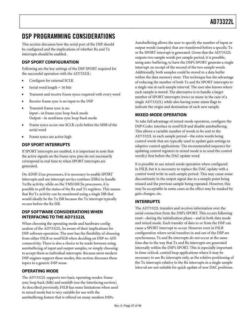
AD73322L
Rev. A | Page 37 of 48
DSP PROGRAMMING CONSIDERATIONS This section discusses how the serial port of the DSP should be configured and the implications of whether Rx and Tx interrupts should be enabled.
DSP SPORT CONFIGURATION Following are the key settings of the DSP SPORT required for the successful operation with the AD73322L:
• Configure for external SCLK
• Serial word length = 16 bits
• Transmit and receive frame syncs required with every word
• Receive frame sync is an input to the DSP
• Transmit frame sync is an: Input—in frame sync loop-back mode Output—in nonframe sync loop-back mode
• Frame syncs occur one SCLK cycle before the MSB of the serial word
• Frame syncs are active high
DSP SPORT INTERRUPTS If SPORT interrupts are enabled, it is important to note that the active signals on the frame sync pins do not necessarily correspond in real time to when SPORT interrupts are generated.
On ADSP-21xx processors, it is necessary to enable SPORT interrupts and use interrupt service routines (ISRs) to handle Tx/Rx activity, while on the TMS320CSx processors, it is possible to poll the status of the Rx and Tx registers. This means that Rx/Tx activity can be monitored using a single ISR that would ideally be the Tx ISR because the Tx interrupt typically occurs before the Rx ISR.
DSP SOFTWARE CONSIDERATIONS WHEN INTERFACING TO THE AD73322L When choosing the operating mode and hardware config-uration of the AD73322L, be aware of their implications for DSP software operation. The user has the flexibility of choosing from either FSLB or nonFSLB when deciding on DSP-to-AFE connectivity. There is also a choice to be made between using autobuffering of input and output samples, or simply choosing to accept them as individual interrupts. Because most modern DSP engines support these modes, this section discusses these topics in a generic DSP sense.
OPERATING MODE The AD73322L supports two basic operating modes: frame sync loop back (fslb) and nonfslb (see the Interfacing section). As described previously, FSLB has some limitations when used in mixed mode but is very suitable for use with the autobuffering feature that is offered on many modern DSPs.
Autobuffering allows the user to specify the number of input or output words (samples) that are transferred before a specific Tx or Rx SPORT interrupt is generated. Given that the AD73322L outputs two sample words per sample period, it is possible, using auto-buffering, to have the DSP’s SPORT generate a single interrupt on receipt of the second of the two sample words. Additionally, both samples could be stored in a data buffer within the data memory store. This technique has the advantage of reducing the number of both Tx and Rx SPORT interrupts to a single one at each sample interval. The user also knows where each sample is stored. The alternative is to handle a larger number of SPORT interrupts (twice as many in the case of a single AD73322L) while also having some status flags to indicate the origin and destination of each new sample.
MIXED-MODE OPERATION To take full advantage of mixed-mode operation, configure the DSP/Codec interface in nonFSLB and disable autobuffering. This allows a variable number of words to be sent to the AD73322L in each sample period—the extra words being control words that are typically used to update gain settings in adaptive control applications. The recommended sequence for updating control registers in mixed mode is to send the control word(s) first before the DAC update word.
It is possible to use mixed-mode operation when configured in FSLB, but it is necessary to replace the DAC update with a control word write in each sample period. This may cause some discontinuity in the output signal due to a sample point being missed and the previous sample being repeated. However, this may be acceptable in some cases as the effect may be masked by gain changes, etc.
INTERRUPTS The AD73322L transfers and receives information over the serial connection from the DSP’s SPORT. This occurs following reset—during the initialization phase—and in both data mode and mixed mode. Each transfer of data to or from the DSP can cause a SPORT interrupt to occur. However even in FSLB configuration where serial transfers in and out of the DSP are synchronous, Tx and Rx interrupts do not occur at the same time due to the way that Tx and Rx interrupts are generated internally within the DSP’s SPORT. This is especially important in time-critical, control loop applications where it may be necessary to use Rx interrupts only, as the relative positioning of the Tx interrupts relative to the Rx interrupts in a single sample interval are not suitable for quick update of new DAC positions.
AD73322L
Rev. A | Page 38 of 48
INITIALIZATIONFollowing reset, the AD73322L is in its default condition, which ensures that the device is in control mode and must be programmed or initialized from the DSP to start conversions. Because communications between AD73322L and the DSP are interrupt driven, it is usually not practical to embed the initial-ization codes into the body of the initialization routine. It is more practical to put the sequence of initialization codes in a data (or program) memory buffer and to access this buffer with a pointer that is updated on each interrupt. If a circular buffer is used, it allows the interrupt routine to check when the circular buffer pointer has wrapped around—at which point the initialization sequence is complete.
In FSLB configurations, a single control word per codec per sample period is sent to the AD73322L. In nonFSLB, it is possible to initialize the device in a single sample period provided the SCLK rate is programmed to a high rate. It is also possible to use autobuffering, in which case an interrupt is generated when the entire initialization sequence has been sent to the AD73322L.
RUNNING THE AD73322L WITH ADCS OR DACS IN POWER-DOWN The programmability of the AD73322L allows the user flexi-bility in choosing what sections of the AD73322L need to be powered up. This allows better matching of the power con-sumption and application requirements, because the AD73322L offers two ADCs and two DACs in any combination. The AD73322L always interfaces to the DSP in a standard way, regardless of what ADC or DAC sections are enabled or disabled. Therefore, the DSP expects to receive two ADC samples per sample period and to transmit two DAC samples per sample period. If a particular ADC is disabled (in power-down) then its sample value is invalid. Likewise, a sample sent to a DAC which is disabled has no effect.
There are two distinct phases of operation of the AD73322L: initialization of the device via each codec section’s control registers, and operation of the converter sections of each codec. The initialization phase involves programming the control registers of the AD73322L to ensure the required operating characteristics such as sampling rate, serial clock rate, and I/O gain. There are several ways in which the DSP can be programmed to initialize the AD73322L. These range from hard-coding a sequence of DSP SPORT Tx register writes with constants used for the initialization words, to putting the initialization sequence in a circular data buffer and using an autobuffered transmit sequence.
Hard-coding involves creating a sequence of writes to the DSP’s SPORT Tx buffer, which are separated by loops or instructions that idle and wait for the next Tx interrupt to occur, as shown in the code that follows. ax0 = b#1000100100000100; tx0 = ax0; idle; wait for tx register to send current word
The circular buffer approach can be useful if a long initiali-zation sequence is required. The list of initialization words is put into the buffer in the required order: .VAR/DM/RAM/CIRC init_cmds[16]; Codec init sequence .VAR/DM/RAM stat_flag; .INIT init_cmds: b # 1 0 0 0 1 0 0 1 0 0 0 0 0 1 0 0 , b # 1 0 0 0 0 0 0 1 0 0 0 0 0 1 0 0 , b # 1 0 0 0 1 0 1 0 1 1 1 1 1 0 0 1 , b # 1 0 0 0 0 0 1 0 1 1 1 1 1 0 0 1 , b # 1 0 0 0 1 0 1 1 0 0 0 0 0 0 0 0 , b # 1 0 0 0 0 0 1 1 0 0 0 0 0 0 0 0 , b # 1 0 0 0 1 1 0 0 0 0 0 0 0 0 0 0 , b # 1 0 0 0 0 1 0 0 0 0 0 0 0 0 0 0 , b # 1 0 0 0 1 1 0 1 0 0 0 0 0 0 0 0 , b # 1 0 0 0 0 1 0 1 0 0 0 0 0 0 0 0 , b # 1 0 0 0 1 1 1 0 0 0 0 0 0 0 0 0 , b # 1 0 0 0 0 1 1 0 0 0 0 0 0 0 0 0 , b # 1 0 0 0 1 1 1 1 0 0 0 0 0 0 0 0 , b # 1 0 0 0 0 1 1 1 0 0 0 0 0 0 0 0 , b # 1 0 0 0 1 0 0 0 0 0 0 1 0 0 0 1 , b # 1 0 0 0 0 0 0 0 0 0 0 1 0 0 0 1 ;
The DSP program initializes pointers to the top of the buffer: i3 = ^init_cmds; 13 = %init_cmds;
and puts the first entry in the DSP’s transmit buffer so that it is available at the first SDOFS pulse: ax0 = dm(i3,m1); tx0 = ax0;
The DSP’s transmit interrupt is enabled: imask = b#0001000000;
AD73322L
Rev. A | Page 39 of 48
At each occurrence of an SDOFS pulse, the DSP’s transmit buffer contents are sent to the SDI pin of the AD73322L. This also causes a subsequent DSP Tx interrupt which transfers the initialization word, pointed to by the circular buffer pointer, to the Tx buffer. The buffer pointer is updated to point to the next unsent initialization word. When the circular buffer pointer wraps around, which happens after the last word has been accessed, it indicates that the initialization phase is complete. This can be done manually in the DSP using a simple address check, or autobuffered mode can be used to complete the transfer automatically. txcdat: ar = dm(stat_flag); ar = pass ar; if eq rti; ena sec_reg; ax0 = dm (i3, m1); tx0 = ax0; ax0 = i3; ay0 = ^init_cmds; ar = ax0 - ay0; if gt rti; ax0 = 0x00; dm (stat_flag) = ax0; rti;
In the main body of the program the code loops, waiting for the initialization sequence to be completed. check_init: ax0 = dm (stat_flag); af = pass ax0; if ne jump check_init;
Because the AD73322L is effectively a cascade of two codec units, it is important to observe the following restrictions in the sequence of sending initialization words to the two codecs. It is preferable to send pairs of control words for the corresponding control registers in each codec, and it is essential to send the control word for codec 2 before that for codec 1. Control Registers A and B contain settings, such as sampling rate, serial clock rate, etc., which critically require synchronous update in both codecs.
Once the device has been initialized, Control Register A on both codecs is written with a control word which changes the operating mode from program mode to either data mode or mixed control data mode. The device count field, which defaults to 000b, must be programmed to 001b for a single AD73322L device. In data mode or mixed mode, the main function of the device is to return ADC samples from both codecs and to accept DAC words for both codecs. During each sample interval, two ADC samples are returned from the device, while in the same interval two DAC update samples are sent to the device. To reduce the number of interrupts and to reduce complexity, autobuffering can be used to ensure that only one interrupt is generated during each sampling interval.
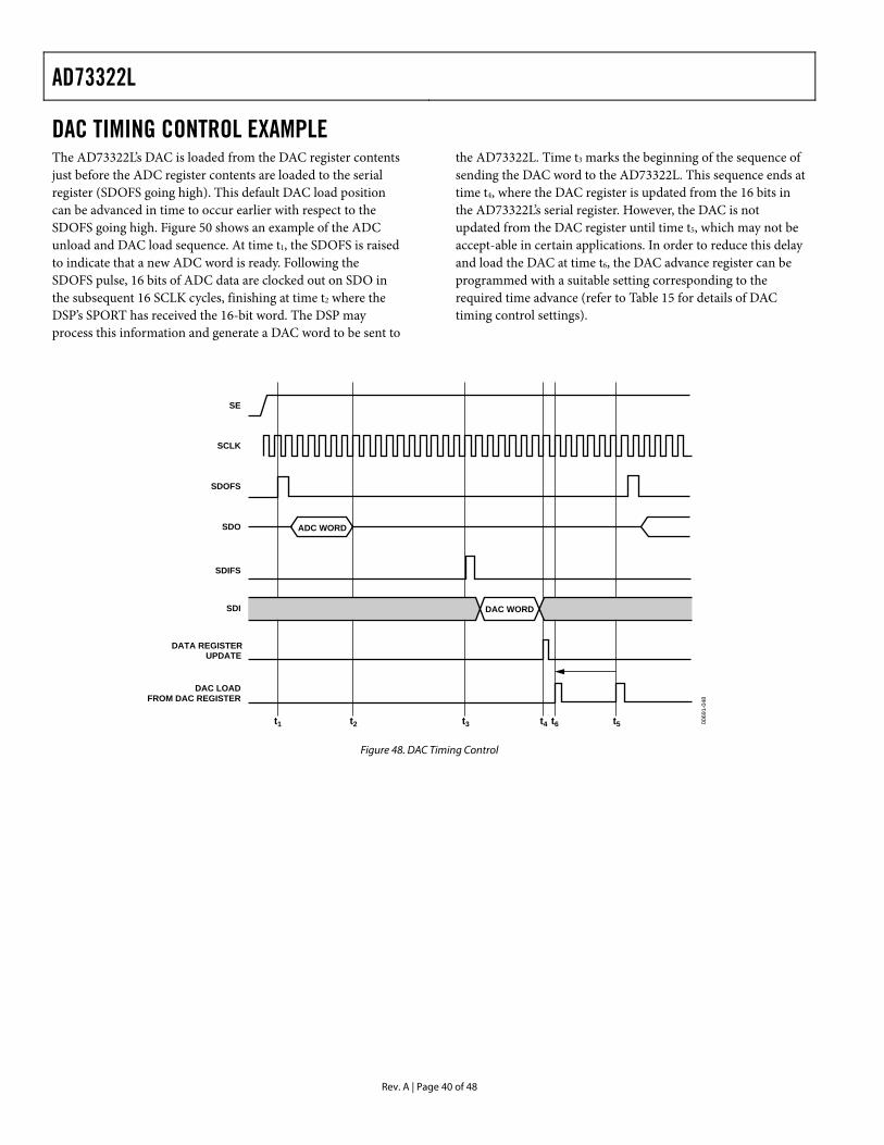
AD73322L
Rev. A | Page 40 of 48
DAC TIMING CONTROL EXAMPLE The AD73322L’s DAC is loaded from the DAC register contents just before the ADC register contents are loaded to the serial register (SDOFS going high). This default DAC load position can be advanced in time to occur earlier with respect to the SDOFS going high. Figure 50 shows an example of the ADC unload and DAC load sequence. At time t1, the SDOFS is raised to indicate that a new ADC word is ready. Following the SDOFS pulse, 16 bits of ADC data are clocked out on SDO in the subsequent 16 SCLK cycles, finishing at time t2 where the DSP’s SPORT has received the 16-bit word. The DSP may process this information and generate a DAC word to be sent to
the AD73322L. Time t3 marks the beginning of the sequence of sending the DAC word to the AD73322L. This sequence ends at time t4, where the DAC register is updated from the 16 bits in the AD73322L’s serial register. However, the DAC is not updated from the DAC register until time t5, which may not be accept-able in certain applications. In order to reduce this delay and load the DAC at time t6, the DAC advance register can be programmed with a suitable setting corresponding to the required time advance (refer to Table 15 for details of DAC timing control settings).
SE
SCLK
SDOFS
SDO
SDIFS
DATA REGISTERUPDATE
DAC LOADFROM DAC REGISTER
t1 t2 t3 t4 t6 t5
ADC WORD
SDI DAC WORD
0069
1-04
8
Figure 48. DAC Timing Control
AD73322L
Rev. A | Page 41 of 48
CONFIGURING AN AD73322L TO OPERATE IN DATA MODE This section describes the typical sequence of control words that are required to be sent to an AD73322L to set it up for data mode operation.1 In this sequence, Registers B, C, and A are programmed before the device enters data mode. This description refers to the steps in Table 27.
At each sampling event, a pair of SDOFS pulses is observed, which causes a pair of control (programming) words to be sent to the device from the DSP. Each pair of control words should program a single register in each Channel. The sequence to be followed is Channel 2 followed by Channel 1.
Step 1 shows the first output sample event following a device reset. The SDOFS signal is raised on both channels2 simulta-neously, which prepares the DSP Rx register to accept the ADC word from Channel 2, while SDOFS from Channel 1 becomes an SDIFS to Channel 2. As the SDOFS of Channel 2 is coupled to the DSP’s TFS and RFS, and to the SDIFS of Channel 1, this event also forces a new control word to be output from the DSP Tx register to Channel 1.3
Step 2 shows the status of the channels following the transmis-sion of the first control word. The DSP has received the output word from Channel 2, while Channel 2 has received the output word from Channel 1. Channel 1 has received the control word destined for Channel 2. At this stage, the SDOFS of both channels are again raised because Channel 2 has received Channel 1’s output word, and as it is not a valid control word addressed to Channel 2, it is passed on to the DSP. Likewise, Channel 1 has received a control word destined for Channel 2—address field is not zero—and it decrements the address field of the control word and passes it on.
Step 3 shows completion of the first series of control word writes. The DSP has received both output words and each channel has received a control word that addresses Control Register B and sets the internal MCLK divider ratio to 1, SCLK rate to DMCLK/2, and sampling rate to DMCLK/256. Both channels are updated simultaneously because both receive the addressed control word at the same time. This is an important factor in cascaded operation as any latency between updating the SCLK or DMCLK of channels can result in corrupted operation. This does not happen in the case of an FSLB config-uration, as shown here, but must be taken into account in a nonFSLB configuration. Another observation of this sequence is that the data-words are received and transmitted in reverse order—that is, the ADC words are received by the DSP, Channel 2 first, then Channel 1 and, similarly, the transmit words from the DSP are sent to Channel 2 first, then to Channel 1. This ensures that all channels are updated at the same time.
Steps 4 to 6 are similar to Steps 1–3, but the user must program Control Register C to power up the analog sections of the device (ADCs, DACs, and reference).
Steps 7 to 9 are similar to Steps 1 to 3, but the user must program Control Register A, with a device count field equal to two channels in cascade, and set the PGM/DATA bit to one to put the channel in data mode.
By Step 10, the programming phase completed, and actual channel data read and write can begin. The words loaded in the serial registers of the two channels at the ADC sampling event contain valid ADC data, and the words written to the channels from the DSP’s Tx register are interpreted as DAC words. The DSP Tx register contains the DAC word for Channel 2.
In Step 11, the first DAC word has been transmitted into the cascade, and the ADC word from Channel 2 has been read from the cascade. The DSP Tx register contains the DAC word for Channel 1. Because the words being sent to the cascade are being interpreted as 16-bit DAC words, the addressing scheme changes from one where the address was embedded in the transmitted word, to one where the serial port counts the SDIFS pulses. When the number of SDIFS pulses received equals the value in the channel count field of Control Register A—the length of the cascade—each channel updates its DAC register with the present word in its serial register.
In Step 11 each channel has received only one SDIFS pulse; Channel 2 received one SDIFS from the SDOFS of Channel 1 when it sent its ADC word, and Channel 1 received one SDIFS pulse when it received the DAC word for Channel 2 from the DSP’s Tx register. Therefore, each channel raises its SDOFS line to pass on the current word in its serial register, and each channel receives another SDIFS pulse.
Step 12 shows the completion of an ADC read and DAC write cycle. Following Step 11, each channel has received two SDIFS pulses that equal the setting of the channel count field in Control Register A. The DAC register in each channel is up-dated with the contents of the word that accompanied the SDIFS pulse that satisfied the channel count requirement. The internal frame sync counter is reset to zero and begins counting for the next DAC update cycle.
Steps 10–12 are repeated on each sampling event.
1 Channel 1 and Channel 2 refer to the two AFE sections of the AD73322L. 2 The AD73322L is configured as two channels in cascade. The internal
cascade connections between Channels 1 and 2 are detailed in . The connections SDI/SDIFS are inputs to Channel 1, while SDO/SDOFS are outputs from Channel 2.
Figure 23
3 This sequence assumes that the DSP SPORT’s Rx and Tx interrupts are enabled. Ensure that there is no latency (separation) between control words in a cascade configuration. This is especially the case when programming Control Registers A and B as they must be updated synchronously in each channel.
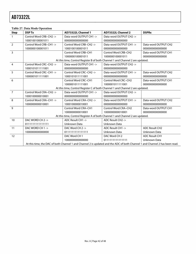
AD73322L
Rev. A | Page 42 of 48
Table 27. Data Mode Operation Step DSP Tx AD73322L Channel 1 AD73322L Channel 2 DSPRx 1 Control Word CRB–CH2 -> Data-word OUTPUT CH1 -> Data-word OUTPUT CH2 -> 1000100100001011 0000000000000000 0000000000000000 2 Control Word CRB–CH1 -> Control Word CRB–CH2 -> Data-word OUTPUT CH1 -> Data-word OUTPUT CH2 1000000100001011 1000100100001011 0000000000000000 0000000000000000 3 Control Word CRB–CH1 Control Word CRB–CH2 Data-word OUTPUT CH1 1000000100001011 1000000100001011 0000000000000000 At this time, Control Register B of both Channel 1 and Channel 2 are updated. 4 Control Word CRC–CH2 -> Data-word OUTPUT CH1 -> Data-word OUTPUT CH2 -> 1000101011111001 0000000000000000 0000000000000000 5 Control Word CRC–CH1 -> Control Word CRC–CH2 -> Data-word OUTPUT CH1 -> Data-word OUTPUT CH2 1000001011111001 1000101011111001 0000000000000000 0000000000000000 6 Control Word CRC–CH1 Control Word CRC–CH2 Data-word OUTPUT CH1 1000001011111001 1000001011111001 0000000000000000 At this time, Control Register C of both Channel 1 and Channel 2 are updated. 7 Control Word CRA–CH2 -> Data-word OUTPUT CH1 -> Data-word OUTPUT CH2 -> 1000100000010001 0000000000000000 0000000000000000 8 Control Word CRA–CH1 -> Control Word CRA–CH2 -> Data-word OUTPUT CH1 -> Data-word OUTPUT CH2 1000000000010001 1000100000010001 0000000000000000 0000000000000000 9 Control Word CRA–CH1 Control Word CRA–CH2 Data-word OUTPUT CH1 1000000000010001 1000000000010001 0000000000000000 At this time, Control Register A of both Channel 1 and Channel 2 are updated. 10 DAC WORD CH 2 -> ADC Result CH1 -> ADC Result CH2 -> 0111111111111111 Unknown Data Unknown Data 11 DAC WORD CH 1 -> DAC Word CH 2 -> ADC Result CH1 -> ADC Result CH2 1000000000000000 0111111111111111 Unknown Data Unknown Data 12 DAC Word CH 1 DAC Word CH 2 ADC Result CH1 1000000000000000 0111111111111111 Unknown Data At this time, the DAC of both Channel 1 and Channel 2 is updated and the ADC of both Channel 1 and Channel 2 has been read.
AD73322L
Rev. A | Page 43 of 48
CONFIGURING AN AD73322L TO OPERATE IN MIXED MODE This section describes a typical sequence of control words that would be sent to an AD73322L to configure it for operation in mixed mode.1 It is not intended to be a definitive initialization sequence, but shows users the typical input/output events that occur in the programming and operation phases2. The text in this section refers to the steps in Table 28.
Steps 1–5 detail the transfer of the control words to Control Register A, which programs the device for mixed-mode operation. Step 1 shows the first output sample event following a device reset. The SDOFS signal is simultaneously raised on both channels, which prepares the DSP Rx register to accept the ADC word from Channel 2, while SDOFS from Channel 1 becomes an SDIFS to Channel 2. The cascade is configured as nonFSLB, which means that the DSP has control over what is transmitted to the cascade3 and, in this case, does not transmit to the devices until both output words have been received from the AD73322L.
Step 2 shows the status of the channels following receipt of the Channel 2 output word. The DSP has received the ADC word from Channel 2, while Channel 2 has received the output word from Channel 1. At this stage, the SDOFS of Channel 2 is again raised because Channel 2 has received Channel 1’s output word and, as it is not addressed to Channel 2, passes it on to the DSP.
In Step 3, the DSP has received both ADC words. Typically, an interrupt is generated following reception of the two output words by the DSP (this involves programming the DSP to use autobuffered transfers of two words). The transmit register of the DSP is loaded with the control word destined for Channel 2. This generates a transmit frame-sync (TFS) that is input to the SDIFS input of the AD73322L to indicate the start of transmission.
In Step 4, Channel 1 contains the control word destined for Channel 2. The address field is decremented, SDOFS1 is raised (internally) and the control word is passed on to Channel 2. The Tx register of the DSP has now been updated with the control word destined for Channel 1 (this can be done using auto-buffering of transmit or by handling transmit interrupts following each word sent).
In Step 5, each channel has received a control word that addresses Control Register A, sets the device count field equal to two channels, and programs the channels into mixed mode (MM and PMG/DATA set to one).
Following Step 5, the device has been programmed into mixed mode although none of the analog sections have been powered up (controlled by Control Register C). Steps 6 to 10 detail update of Control Register B in mixed mode. In Steps 6 to 8, the ADC samples, which are invalid because the ADC section is not yet powered up, are transferred to the DSP’s Rx section. In the
subsequent interrupt service routine, the Tx register is loaded with the control word for Channel 2. In Steps 9–10, Channels 1 and 2 are loaded with a control word setting for Control Register B, which programs DMCLK = MCLK, the sampling rate, to DMCLK/256, SCLK = DMCLK/2.
Steps 11 to 17 are similar to Steps 6 to 12 except that Control Register C is programmed to power up all analog sections (ADC, DAC, Reference = 1.2 V, REFOUT). In Steps 16–17, DAC words are sent to the device—both DAC words are necessary because each channel only updates its DAC when the device has counted a number of SDIFS pulses, accompanied by DAC words (in mixed mode, the MSB = 0), that are equal to the device count field of Control Register A4. Because the channels are in mixed mode, the serial port interrogates the MSB of the 16-bit word sent to determine whether it contains DAC data or control information. DAC words should be sent in the sequence Channel 2 followed by Channel 1.
Steps 11 to17 show the control register update and DAC update in a single sample period. Note that this combination is not possible in the FSLB configuration3.
Steps 18 to 25 illustrate a control register readback cycle. In Step 22, both channels have received a control word that addresses Control Register C for readback (Bit 14 of the control word = 1). When the channels receive the readback request, the register contents are loaded to the serial registers, as shown in Step 23. SDOFS is raised in both channels, which causes these readback words to be shifted out toward the DSP. In Step 24, the DSP has received the Channel 2 readback word, while Channel 2 has received the Channel 1 readback word (note that the address field in both words has been decremented to 111b). In Step 25, the DSP has received the Channel 1 readback word (its address field has been further decremented to 110b).
Steps 26 to 30 detail an ADC and DAC update cycle using the nonFSLB configuration. In this case, no control register update is required.
1 Channel 1 and Channel 2 refer to the two AFE sections of the AD73322L. 2 This sequence assumes that the DSP SPORT’s Rx and Tx interrupts are
enabled. Ensure there is no latency (separation) between control words in a cascade configuration. This is especially the case when programming Control Registers A and B.
3 Mixed-mode operation with the FSLB configuration is more restricted in that the number of words sent to the cascade equals the number of channels in the cascade. This means that DAC updates may need to be substituted with a register write or read. Using the FSLB configuration introduces a corruption of the ADC samples in the sample period following a control register write. This corruption is predictable and can be corrected in the DSP. The ADC word is treated as a control word and the device address field is decremented in each channel that it passes through before being returned to the DSP.
4 In mixed mode, DAC update is done using the same SDIFS counting scheme as in normal data mode, with the exception that only DAC words (MSB set to zero) are recognized as being able to increment the frame sync counters.
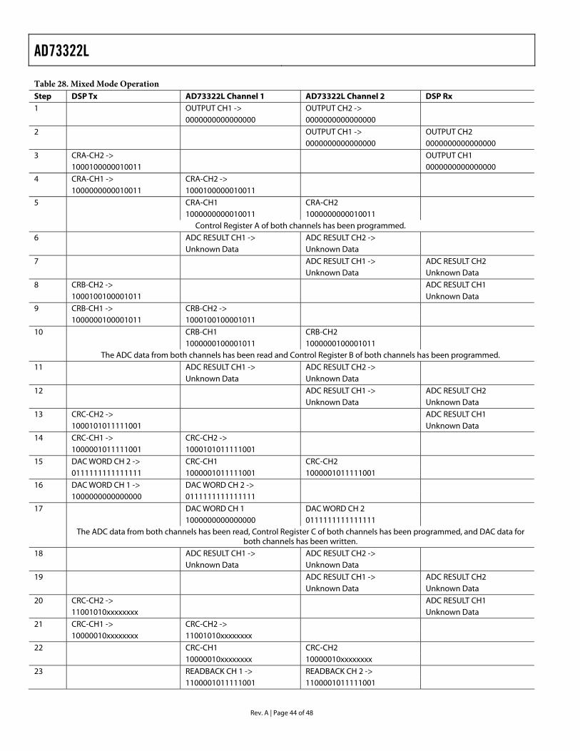
AD73322L
Rev. A | Page 44 of 48
Table 28. Mixed Mode Operation Step DSP Tx AD73322L Channel 1 AD73322L Channel 2 DSP Rx 1 OUTPUT CH1 -> OUTPUT CH2 -> 0000000000000000 0000000000000000 2 OUTPUT CH1 -> OUTPUT CH2 0000000000000000 0000000000000000 3 CRA-CH2 -> OUTPUT CH1 1000100000010011 0000000000000000 4 CRA-CH1 -> CRA-CH2 -> 1000000000010011 1000100000010011 5 CRA-CH1 CRA-CH2 1000000000010011 1000000000010011 Control Register A of both channels has been programmed. 6 ADC RESULT CH1 -> ADC RESULT CH2 -> Unknown Data Unknown Data 7 ADC RESULT CH1 -> ADC RESULT CH2 Unknown Data Unknown Data 8 CRB-CH2 -> ADC RESULT CH1 1000100100001011 Unknown Data 9 CRB-CH1 -> CRB-CH2 -> 1000000100001011 1000100100001011 10 CRB-CH1 CRB-CH2 1000000100001011 1000000100001011 The ADC data from both channels has been read and Control Register B of both channels has been programmed. 11 ADC RESULT CH1 -> ADC RESULT CH2 -> Unknown Data Unknown Data 12 ADC RESULT CH1 -> ADC RESULT CH2 Unknown Data Unknown Data 13 CRC-CH2 -> ADC RESULT CH1 1000101011111001 Unknown Data 14 CRC-CH1 -> CRC-CH2 -> 1000001011111001 1000101011111001 15 DAC WORD CH 2 -> CRC-CH1 CRC-CH2 0111111111111111 1000001011111001 1000001011111001 16 DAC WORD CH 1 -> DAC WORD CH 2 -> 1000000000000000 0111111111111111 17 DAC WORD CH 1 DAC WORD CH 2 1000000000000000 0111111111111111 The ADC data from both channels has been read, Control Register C of both channels has been programmed, and DAC data for
both channels has been written. 18 ADC RESULT CH1 -> ADC RESULT CH2 -> Unknown Data Unknown Data 19 ADC RESULT CH1 -> ADC RESULT CH2 Unknown Data Unknown Data 20 CRC-CH2 -> ADC RESULT CH1 11001010xxxxxxxx Unknown Data 21 CRC-CH1 -> CRC-CH2 -> 10000010xxxxxxxx 11001010xxxxxxxx 22 CRC-CH1 CRC-CH2 10000010xxxxxxxx 10000010xxxxxxxx 23 READBACK CH 1 -> READBACK CH 2 -> 1100001011111001 1100001011111001
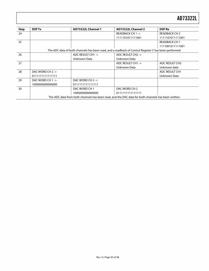
AD73322L
Rev. A | Page 45 of 48
Step DSP Tx AD73322L Channel 1 AD73322L Channel 2 DSP Rx 24 READBACK CH 1 -> READBACK CH 2 1111101011111001 1111101011111001 25 READBACK CH 1 1111001011111001 The ADC data of both channels has been read, and a readback of Control Register C has been performed. 26 ADC RESULT CH1 -> ADC RESULT CH2 -> Unknown Data Unknown Data 27 ADC RESULT CH1 -> ADC RESULT CH2 Unknown Data Unknown data 28 DAC WORD CH 2 -> ADC RESULT CH1 0111111111111111 Unknown Data 29 DAC WORD CH 1 -> DAC WORD CH 2 -> 1000000000000000 0111111111111111 30 DAC WORD CH 1 DAC WORD CH 2 1000000000000000 0111111111111111 The ADC data from both channels has been read, and the DAC data for both channels has been written.
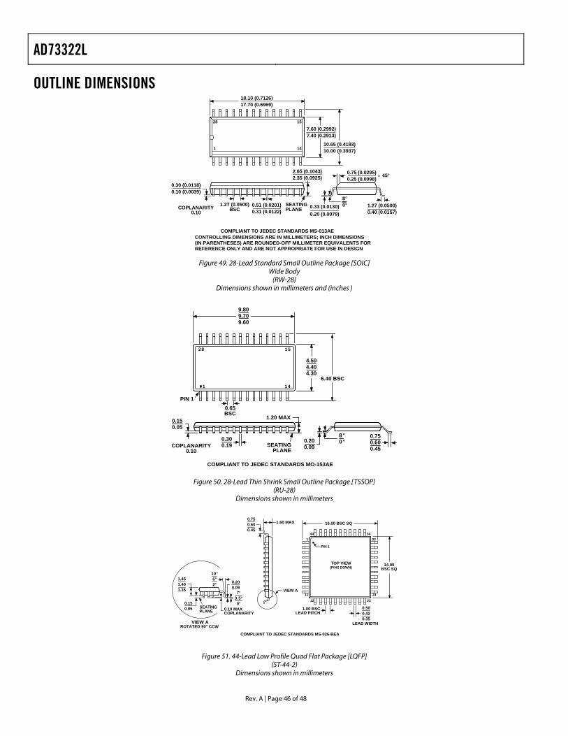
AD73322L
Rev. A | Page 46 of 48
OUTLINE DIMENSIONS
CONTROLLING DIMENSIONS ARE IN MILLIMETERS; INCH DIMENSIONS(IN PARENTHESES) ARE ROUNDED-OFF MILLIMETER EQUIVALENTS FORREFERENCE ONLY AND ARE NOT APPROPRIATE FOR USE IN DESIGN
COMPLIANT TO JEDEC STANDARDS MS-013AE
0.33 (0.0130)0.20 (0.0079)
8°0°
0.75 (0.0295)0.25 (0.0098)
× 45°
1.27 (0.0500)0.40 (0.0157)
SEATINGPLANE
0.30 (0.0118)0.10 (0.0039)
0.51 (0.0201)0.31 (0.0122)
2.65 (0.1043)2.35 (0.0925)
1.27 (0.0500)BSC
28 15
141
18.10 (0.7126)17.70 (0.6969)
10.65 (0.4193)10.00 (0.3937)
7.60 (0.2992)7.40 (0.2913)
COPLANARITY0.10
Figure 49. 28-Lead Standard Small Outline Package [SOIC] Wide Body
(RW-28) Dimensions shown in millimeters and (inches )
2 8 1 5
1 41
8°0°
COMPLIANT TO JEDEC STANDARDS MO-153AE
SEATINGPLANE
COPLANARITY0.10
1.20 MAX
6.40 BSC
0.65BSC
PIN 1
0.300.19
0.200.09
4.504.404.30
0.750.600.45
9.809.709.60
0.150.05
Figure 50. 28-Lead Thin Shrink Small Outline Package [TSSOP] (RU-28)
Dimensions shown in millimeters
VIEW A
TOP VIEW(PINS DOWN)
11
144 34
33
232212
1.00 BSCLEAD PITCH
LEAD WIDTH
16.00 BSC SQ
14.00BSC SQ
1.60 MAX0.750.600.45
0.500.420.35
PIN 1
0.200.09
1.451.401.35
0.10 MAXCOPLANARITY
VIEW AROTATED 90° CCW
SEATINGPLANE
10°6°2°
7°3.5°0°0.15
0.05
COMPLIANT TO JEDEC STANDARDS MS-026-BEA
Figure 51. 44-Lead Low Profile Quad Flat Package [LQFP] (ST-44-2)
Dimensions shown in millimeters
AD73322L
Rev. A | Page 47 of 48
ORDERING GUIDE Model Temperature Range Package Description Package Option AD73322LAR −40°C to +85°C Wide Body SOIC RW-28
AD73322LAR-REEL −40°C to +85°C Wide Body SOIC RW-28
AD73322LAR-REEL7 −40°C to +85°C Wide Body SOIC RW-28
AD73322LARU −40°C to +85°C Thin Shrink TSSOP RU-28
AD73322LARU-REEL −40°C to +85°C Thin Shrink TSSOP RU-28
AD73322LARUZ1 −40°C to +85°C Thin Shrink TSSOP RU-28
AD73322LARUZ-REEL1 −40°C to +85°C Thin Shrink TSSOP RU-28
AD73322LAST −40°C to +85°C Plastic Thin Quad Flatpack (LQFP) ST-44A
AD73322LAST-REEL −40°C to +85°C Plastic Thin Quad Flatpack (LQFP) ST-44A
AD73322LYR −40°C to +105°C Wide Body SOIC RW-28
AD73322LYR-REEL −40°C to +105°C Wide Body SOIC RW-28
AD73322LYR-REEL7 −40°C to +105°C Wide Body SOIC RW-28
AD73322LYRU −40°C to +105°C Thin Shrink TSSOP RU-28
AD73322LYRU-REEL −40°C to +105°C Thin Shrink TSSOP RU-28
AD73322LYST −40°C to +105°C Plastic Thin Quad Flatpack (LQFP) ST-44A
AD73322LYST-REEL −40°C to +105°C Plastic Thin Quad Flatpack (LQFP) ST-44A
1 Z = Pb-free part.
AD73322L
Rev. A | Page 48 of 48
NOTES
© 2004 Analog Devices, Inc. All rights reserved. Trademarks and registered trademarks are the property of their respective owners. C00691–0–12/04(A)