advanced mixers - university of california,...
TRANSCRIPT

Berkeley
Advanced Mixers
Prof. Ali M. Niknejad
U.C. BerkeleyCopyright c© 2014 by Ali M. Niknejad
Niknejad Advanced IC’s for Comm
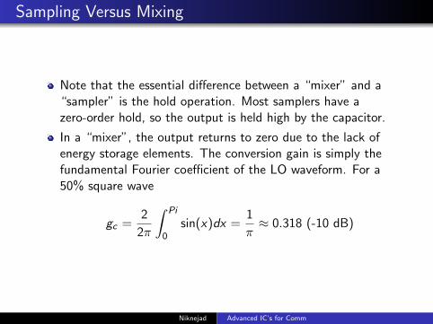
Sampling Versus Mixing
Note that the essential difference between a “mixer” and a“sampler” is the hold operation. Most samplers have azero-order hold, so the output is held high by the capacitor.
In a “mixer”, the output returns to zero due to the lack ofenergy storage elements. The conversion gain is simply thefundamental Fourier coefficient of the LO waveform. For a50% square wave
gc =2
2π
∫ Pi
0sin(x)dx =
1
π≈ 0.318 (-10 dB)
Niknejad Advanced IC’s for Comm

Sampling
For a ZOH sampler, we can model it as an ideal samplerfollowed by an a LPF with bandwidth 1/TD . Note that TD isthe duty cycle over which the output is held. Assume TD issmall so we can model the system as follows:
yout(t) = (p(t) · x(t)) ∗ h(t)
Yout(f ) = (P(f ) ∗ X (f ))H(f )
For a sinusoidal input, we have
X (f ) =1
2(δ(f − fx) + δ(f + fx))
and
P(f ) =1
TLO
∞∑n=−∞
δ(f − nfLO)
Niknejad Advanced IC’s for Comm

Sampling
Taking the convolution of X and P, we note that things don’toverlap unless the input is shifted to the peaks of P
X (f )∗P(f ) =1
2TLO
∞∑n=−∞
(δ(f − nfLO − fx) + δ(f − nfLO + fx))
The hold action can be modeled by a filter with constantfinite impulse response of duration TD . Taking the LaplaceTransform, we get a sinc frequency response.
H(f ) =sin(πfTD)
πfe−jπfTD = TDsinc(πfTD)e−jπfTD
Niknejad Advanced IC’s for Comm

Sampling Conversion Gain
-3 -2 -1 1 2 3
0.2
0.4
0.6
0.8
1.0
Finally, multiplying by the sinc with our impulse train, we getthe overall transfer function. For a IF frequency, reducing thehold time improves the gain of the system. This is kind of anon-intuitive result !
There’s actually a trade-off between the bandwidth of the IFand the hold time, so there’s no free lunch.
Niknejad Advanced IC’s for Comm

Tayloe’s Sampling Receiver
Product detector and method therefor, US Patent 6230000 B1
Note that the mixer is realized by four samplers, eachsampling with 25% duty cycle.
Such a sampler has I/Q quadrature down-conversion and isbalanced.
As we have seen, this bilateral mixer also creates anarrowband RF filtering effect which is beneficial for rejectionof blocker signals.
Niknejad Advanced IC’s for Comm

Harmonic Reject (HR) Mixers
Niknejad Advanced IC’s for Comm

The Need for Harmonic Rejection
If the RF bandwidth is wider than an octave, then harmonicsof the LO are downconverter to the same IF and corrupt thedesired signal.
Imagine operating a receiver at 800 MHz. A PA operating at3X this frequency or 2400 MHz will couple into the receivechain and get downconverter by the third harmonic of the LO.Even with an Rx filter, the coupled signal may be very strong(30 dB of isolation implies a 0 dBm 3rd harmonic blocker)
Cable receivers are among the systems that process very wideswaths of bandwidth. Reconfigurable LTE transceivers operatefrom 500 MHz to 3600 MHz and have HR requirements.
Wideband Software Defined Radios (SDR) also need it forsimilar reasons.
Niknejad Advanced IC’s for Comm

Why Mixers Like Harmonics
Even if we drive the LO with a sine wave, as long as theamplitude exceeds the threshold voltage of the switching, thenthe output is steered more like a square wave, which is rich inharmonics.
s(t) =4
π
∞∑n=1
sin(2π(2n − 1)fLOt)
2n − 1
Niknejad Advanced IC’s for Comm

How to Synthesize a Sine Wave?
4.3 Harmonic-Rejection Background 83
As the sampling rate is pushed even higher, the resulting SHS waveform will have
even fewer harmonics. Intuitively this makes sense by inspecting the time-domain signal
F T/2 -T/2
1
so(t)
… … t
T
-1
0 -5/T 5/T 1/T -1/T 3/T -3/T
|So(f)|
…… f
f
F T/2 -T/2
1
so(t)
… … t
T
-1
0 -5/T 5/T 1/T -1/T 3/T -3/T
|So(f)|
…… f 7/T -7/T
F 0 -5/T 5/T 1/T -1/T 3/T -3/T
|So(f)|
……
-9/T -7/T 7/T 9/T T/2 -T/2
1
so(t)
…
… t
T
-1
(c)
(a)
(b)
Figure 4.10 Sample and hold operation on sinusoid in time and frequency domains for three sampling frequencies. (a) fs=2fi. (b) fs=4fi. (c) fs=8fi.
Notice that sampling a sine wave produces a square wave. Ifwe oversample the sine wave eight times per cycle, weproduce a staircase approximation to the sine wave.
The key observation is that this waveform is free from the 3rdand 5th harmonic! Can we somehow use this waveform ?
Niknejad Advanced IC’s for Comm

Summing Four Square Waves
4.4 Harmonic-Rejection Principles 89
negative and positive peaks and consequently, the waveform contains two fewer edges in
one period leading to one less square wave. It will be shown in later sections that this
reduces the hardware requirement in the implementation. Generation of the signal, ss(t),
which is an SHS waveform, is the key element to the rejection of unwanted harmonics in
the harmonic-rejection mixer presented in the following section.
The square waves illustrated in Figure 4.14 need to be scaled in amplitude and
phase shifted appropriately to reject the third and fifth harmonics. Signal p0(t) is scaled
by a factor of 2 compared to both p1(t) and p2(t). Furthermore, compared to p0(t), p1(t)
is shifted in time by T/8 to the right and p2(t) is shifted by T/8 to the left. This time shift
… …t
… …t
… …t
T/16
p0(t)
p2(t)
ss(t)
t=0
t=0
… …t
p1(t)
t=0
t=0
1
1
T/2 T -T/2
T/2 T -T/2
T/2 T -T/2
T/2 T -T/2
2
Figure 4.14 SHS waveform resulting from shifting of sampling position and the square waves which compose the SHS waveform. The staircase approximation to sine can be synthesized by
summing three square waves of the right magnitude.
Niknejad Advanced IC’s for Comm

Fourier Series of Square Waves
The wave p0(t) is a 50% duty cycle square wave
p0(t) =4√
2
π(cos(ωt)− 1
3cos(3ωt)+
1
5cos(5ωt)− 1
7cos(7ωt)+· · · )
The waveform p1(t) is just a time and amplitude shiftedversion of p0(t)
p1(t) =2√
2
π(cos(ωt) +
1
3cos(3ωt)− 1
5cos(5ωt)− 1
7cos(7ωt) + · · · )+
2√
2
π(sin(ωt)− 1
3sin(3ωt)− 1
5sin(5ωt) +
1
7sin(7ωt) + · · · )
Niknejad Advanced IC’s for Comm

Synthesizing a Sine from Squares (II)
Similarly, p2(t) is also a time shifted copy
p2(t) =2√
2
π(cos(ωt) +
1
3cos(3ωt)− 1
5cos(5ωt)− 1
7cos(7ωt) + · · · )+
2√
2
π(− sin(ωt) +
1
3sin(3ωt) +
1
5sin(5ωt)− 1
7sin(7ωt) + · · · )
The desired waveform, a sum of the three, is free from 3ω and5ω
p(t) = p0(t) + p1(t) + p2(t) =8√
2
π(cos(ωt)− 1
7cos(7ωt) + · · · )
Niknejad Advanced IC’s for Comm

Weldon/Berkeley Architecture 4.5 Harmonic-Rejection Mixer 99
The scaling potentially could have been achieved by scaling the load of the three
mixers. However, in this case the current from each mixer is summed and an output
voltage is generated through a single shared load. Therefore, scaling the load is not
possible.
Another potential method to scale the output would have been scaling the
magnitude of the input signal. This would have required an additional amplifier thus
adding to the overall complexity.
The scaling was accomplished by adjusting the gm of the input device. Recall
from Equation (4.22) that 2 scaling is needed on one sub-mixer. This is accomplished
in the HRM by scaling the bias current source and the W/L ratio of the input devices. To
2Ibias
Vout
Vin
LO45
Ibias
LO-45 LO0
Ibias
RLRL
(W/L)inI
(W/L)in 2(W/L)in 2(W/L)in (W/L)inI
(W/L)in
(W/L)swI
(W/L)sw (W/L)swI
(W/L)sw2(W/L)sw 2(W/L)sw
Figure 4.16 Simplified circuit diagram of the harmonic-rejection mixer. Three parallel mixers are used, each driven by p0(t), p1(t),and p2(t). We must scale the devices appropriately to realizethe right amplitude (need
√2) [Weldon]
Niknejad Advanced IC’s for Comm

Matching Requirements
4.6 Matching in HRM 109
amount by which the third and fifth harmonics are suppressed, as compared with the
harmonics from the single square wave, is defined as the third harmonic rejection or HR3,
and the fifth harmonic rejection or HR5. This is the relevant figure of merit because in
typical switching mixer the input is multiplied by a square wave but in this case the input
is multiplied by the SHS waveform. Therefore comparing the output of the HRM to
square wave represents the relative improvement in the suppression of the harmonics.
Based on the harmonics of a square wave from Equation (4.5), the relationship
between and HD3 in dB is given by
dB5.9
31log20
3
33
�
¸¹·
¨©§�
HR
HRHD (4.42)
and similarly
.dB14
51log20
5
55
�
¸¹·
¨©§�
HR
HRHD (4.43)
square wave
HR3
T
T2S
(1+')p0(t+TT/2S)
p2(t)
p1(t)1
1
2 (1+D)
¦
fLO 3fLO 5fLO 7fLOf
HR5
t
t
t
HD5HD3
Figure 4.17 Graphical representation of HR3 and HR5. Time mismatch and/or amplitude mismatch leads to finite 3rdand 5th.
Niknejad Advanced IC’s for Comm

Matching Requirements (3rd)
Chapter 4 Harmonic-Rejection Mixer 112
A plot of the fifth harmonic rejection as function of phase and gain error is shown
in Figure 4.19. For low values of phase error, HR5 approaches HR3. For small phase
errors, the gain mismatch is the dominant source of error. From Equations (4.46) and
(4.47) it is clear that as the phase error approaches zero, the values of HR3 and HR5
converge. However, as the phase error gets larger, the HR5 decreases faster than HR3 due
to its greater dependence on phase error. This greater dependence is evident by the fact
that HR5 is a proportional the cosine of 5T while the third harmonic rejection is a
proportional to the cosine of 3T.
Figure 4.18 Third harmonic rejection as a function of gain and phase error.
0 0.5 1 1.5 2 2.5 3 3.5 4 10
15
20
25
30
35
40
T (degrees)
HR 3 (dB)
D=0.01
D=0.05
D=0.1
Good HR requires very good matching !
Niknejad Advanced IC’s for Comm

Matching Requirements (5th) 4.6 Matching in HRM 113
The specifications of the system will determine the tolerances in both the gain and
phase mismatch. Gain mismatches in the sub-mixers are a function of device mismatch.
The two main sources of gain mismatch are the current sources and the input differential
pairs. The overall mixer gain does not depend strongly on matching in the switches and
therefore mismatch between sets of switches is less of a problem.
Device mismatch is typically caused by mismatch in the device geometry and
threshold voltage mismatch. Large device sizes can limit mismatch caused due to device
geometry and large gate to source bias voltages can reduce the effects of threshold
voltage mismatch. Unfortunately, having both large device geometries and large bias
voltages requires a larger current and thus more power.
Figure 4.19 Fifth harmonic rejection as a function of gain and phase error.
0 0.5 1 1.5 2 2.5 3 3.5 4 5
10
15
20
25
30
35
40
T (degrees)
HR 5 (dB)
D =0.01
D=0.05
D=0.1
Niknejad Advanced IC’s for Comm
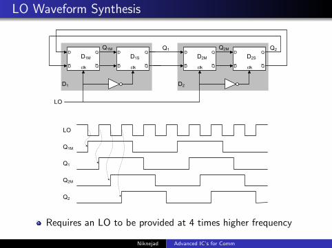
LO Waveform Synthesis
4.8 LO Phase Generation 121
A master-slave flip-flop, as the name implies, is composed of a master flip-flop
and slave flip-flop. Expanding each D flip-flop, by showing both the master and the
slave flip-flops, and including the differential signal path, results in the diagram shown in
Figure 4.22. Each MS D flip-flop is composed of two negative edge triggered D flip-
flops, a master and a slave. Therefore, internal to the MS flip-flop, are internal nodes,
designated, Q1M and Q2M, which are the outputs of each master flip-flop. The outputs
from the slave flip-flops are simply the output of the composite MS D flip-flop and are
given by Q1 and Q2. The complements of these four signals are also present but are not
labeled for the sake of simplicity.
D
LO
Q
clk __ Q
Q1M Q1
__ D clk
Q2MQ
__ Q
D Q2
__ D
LO
Q2
Q1
Q1M
Q2M
D2
D1M
clk
D
__ D
Q
__ Q
D Q
clk __ Q
__ D
D1S D2S D2M
D1
Figure 4.22 Expanded view of divide-by-four and timing diagram. Requires an LO to be provided at 4 times higher frequency
Niknejad Advanced IC’s for Comm

Harmonic Reject Transmitter 5.2 Harmonic Rejection Transmitter Architecture 135
The basic function of the HRT is as follows. The baseband is identical to the
homodyne and heterodyne transmitter which were discussed in Chapter 3 as digital in-
phase and quadrature baseband signals pass through a DAC and then a low-pass filter.
The analog I and Q baseband signals are then up-converted to IF with four HRMs
generating I and Q IF signals. By generating I and Q IF signals the image created in the
up-conversion to RF can be attenuated through the use of an image-rejection RF mixer.
The image-reject configuration uses two RF mixers and I and Q LO1 signals to complete
the up-conversion to RF. By generating I and Q IF signals and then using and image-
reject mixer, the RF filtering requirements are reduced compared to the conventional
heterodyne transmitter. Finally, the RF signal is then amplified by a PA before it passes
through an RF bandpass filter and on to the antenna.
RF Filter
PA 0 90`
LO2
DAC IBB
QBB DAC QIF
fRF
IIF
8 phase generator
= HRM
LO1
Figure 5.1 Block diagram of a Harmonic Rejection Transmitter.
Similar concept applies for the receiver.
Niknejad Advanced IC’s for Comm

Forming Gains at Baseband
Prof. Al Molnar’s MS thesis had this 8-phase passive mixerwith HR suppression [Molnar].
Niknejad Advanced IC’s for Comm
Sub-Harmonic Mixers
Niknejad Advanced IC’s for Comm

Sub-Harmonic Mixer Design
fRF
fLO = 0.5fRF
Sub-Harmonic Mixer
The subharmonic mixer is driven by an LO signal that is aninteger fraction, or subharmonic, of the desired LO frequency.For example, if the RF signal is 2GHz, and the desired LO is2GHz for direct conversion, a subharmonic mixer will bedriven by a 1GHz LO signal. The advantages are:
Lower LO re-radiation through the antenna (LO leakage)Lower LO self mixing (lower DC offset at IF)Relaxed requirement on the device switching speed.Lower LO buffer current
Niknejad Advanced IC’s for Comm
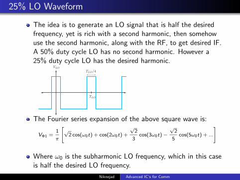
25% LO Waveform
The idea is to generate an LO signal that is half the desiredfrequency, yet is rich with a second harmonic, then somehowuse the second harmonic, along with the RF, to get desired IF.A 50% duty cycle LO has no second harmonic. However a25% duty cycle LO has the desired harmonic.
VLO
TLO
TLO/4
The Fourier series expansion of the above square wave is:
VΦ1 =1
π
[√
2 cos(ω0t) + cos(2ω0t) +
√2
3cos(3ω0t)−
√2
5cos(5ω0t) + ...
]
Where ω0 is the subharmonic LO frequency, which in this caseis half the desired LO frequency.
Niknejad Advanced IC’s for Comm

Sub-Harmonic Mixer
+RF
LO1
LO2
IF
The subharmonic mixer topology uses two identical mixersexcited by two phases of the 25% duty cycles. The RF signalis multiplied by these two delayed 25% LO signals and the IFis added in phase at the output, as shown in the above figure.
Niknejad Advanced IC’s for Comm
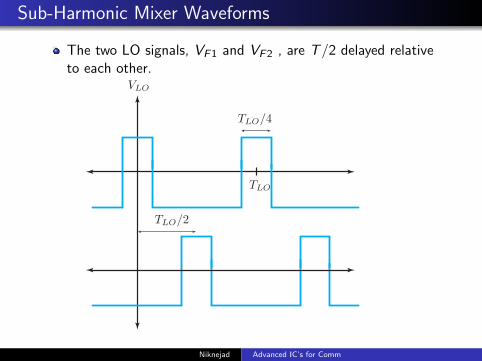
Sub-Harmonic Mixer Waveforms
The two LO signals, VF1 and VF2 , are T/2 delayed relativeto each other.
VLO
TLO
TLO/4
TLO/2
Niknejad Advanced IC’s for Comm

Sub-Harmonic Waveforms
VΦ2 =1
π
[−√
2 cos(ω0t) + cos(2ω0t)−√
2
3cos(3ω0t) +
√2
5cos(5ω0t) + · · ·
]
Looking at the combined IF output of the subharmonic mixerwe can write:
VIF = VRFVΦ1 + VRFVΦ2 = VRF
[2
πcos(2ω0t)
]As seen, the resulting IF output is the product of the RFsignal and an effective LO that has twice the subharmonic LOfrequency, which is in fact the desired LO. The above analysiswas for only one mixer. The question then, how can one buildquadrature subharmonic mixer for both I and Q channels?The answer comes in the way to generate a sin(2ω0t) LOsignal using similar 25% duty cycle signals as follows.
Niknejad Advanced IC’s for Comm

I/Q Sub-Harmonic MixerVLO
TLO
TLO/8
TLO/85
The LO signal LOF3 is delayed T/8 relative to LOF1. LOF4 isdelayed by T/2 relative to LOF3.The Fourier series expansion of the above square waves is:
VΦ3 =1
π
[√
2 cos(ω0t −π
2) + sin(2ω0t) +
√2
3sin(3ω0t −
π
2) +
√2
5cos(5ω0t −
π
2) + ...
]
VΦ4 =1
π
[−√
2 cos(ω0t −π
2) + sin(2ω0t)−
√2
3sin(3ω0t −
π
2)−√
2
5cos(5ω0t −
π
2) + ...
]
Niknejad Advanced IC’s for Comm

Generation of LO
Looking at the combined IF output of the subharmonic mixerwe can write:
VIF Q = VRFVΦ3 + VRFVΦ4 = VRF
[2
πsin(2ω0t)
]In order to generate all 4 phases of the subharmonic LOsignals, a divide by 4 prescalar needs to be used. This meansthe VCO needs to run at 4X the subharmonic LO, 2X the RFsignal for direct conversion.
RF
LO1
LO2
LO4
LO3
IFI
IFQ
2f04f0
÷4
V CO
Niknejad Advanced IC’s for Comm

Sub-Harmonic Realization
LO(+)
LO(−)
IF (+)
IF (−)
LO(+)
LO(−)
RF(+) RF(−)
The above is a simplified implementation of one subharmonicmixer. Since a subharmonic mixer is two mixers in one drivenby the same RF input but has two different LO phases, asingle common Gm stage is used.
Niknejad Advanced IC’s for Comm

Mixer First Architecture
Niknejad Advanced IC’s for Comm

Why Not Mixer First
Getting rid of the LNA seems like a really bad idea. Isn’t anLNA a must ?
The LNA input impedance is matched to the antenna (orfilter) for optimal power transfer into the receiver.Furthermore, the impedance match simplified board designsince transmission lines can be used to bring in the signal fromthe antenna without worrying about any potential impedancetransformation (except length should be minimized to reducelosses).
Niknejad Advanced IC’s for Comm

Why Not (Noise and LO Leakage)
Recall that the LNA is there to minimize the noisecontribution of sub-sequent stages, so it should be designedwith low noise and as high of a gain as possible.
Also the LO signal leakage to the antenna port is minimized,an issue if we remove the LNA.
Niknejad Advanced IC’s for Comm

Maybe ?
In practice the gain is limited by linearity considerations, so atrade-off is made. The first potential benefit of a mixer firstarchitecture is therefore to realize much higher linearity.
If the linearity can be made good enough to reduce oreliminate off-chip filters (LC, SAW, or other bulkycomponents), then there’s a potential win. But this meansmixer noise cannot be too high.
Since the filters introduce about 1-2dB of loss at the input ofthe Rx, perhaps a mixer first Rx can be about 1-2 dB noisierthan an LNA first counterpart.
Niknejad Advanced IC’s for Comm

Cook’s Mixer First Receiver
2758 IEEE JOURNAL OF SOLID-STATE CIRCUITS, VOL. 41, NO. 12, DECEMBER 2006
Fig. 1. Transceiver block diagram.
Fig. 2. Simplified transceiver front-end schematic.
Fig. 3. Quadrature VCO utilizing back gate coupling.
and DC level of the VCO signal driving the switches. Themixer outputs differentially drive a bandpass filter comprisinga pair of linearized CMOS inverters. The filter outputs feedinto a piecewise logarithmic RSSI that hard-limits the signal,providing a square voltage waveform for demodulation.
In its default mode, the receiver uses a low-IF architecturesacrificing image rejection in exchange for cutting power in half.The factor of two lower power in low-IF mode is due to the factthat only a single phase of the VCO is needed and the currentof the baseband chain is also halved. When necessary however,a back-gate coupled quadrature VCO generates I & Q signals(Fig. 3) [14] and two matching BB chains can be enabled. The
Fig. 4. Circuit model for tapped-capacitor resonator.
back-gate coupled VCO architecture was used here because itproduces quadrature outputs without the additional current re-quirements of coupling transistors. In this mode, the receiveruses direct-conversion, achieving DC suppression via the band-pass response of the baseband filters.
1) LC Input Network: A single LC matching network is usedfor both the receiver and transmitter, making a front-end switchunnecessary and reducing inductor count. This network is atapped capacitor resonant transformer (Fig. 1, upper left). Thepurpose of this network is to boost the PA load impedance in thetransmitter and to achieve substantial passive voltage gain in the
Ben Cook, a Berkeley grad working with Prof. Pister,proposed a mixer first receiver and was among the first ofrecent IC designers to realize the benefits of n-path filteringoffered by passive bilateral mixers. [Cook]
Ben Cook and Axel Berny started a company based on thisconcept (Passif) that was acquired by Apple.
Niknejad Advanced IC’s for Comm

Mixer First Motivation and Benefits
Use a passive mixer to achieve very good linearity. Takeadvantage of the bilateral nature to realize a bandpassresponse to improve out-of-band linearity.
Make the system tunable by controlling the LO frequency,rather than tuning capacitors or inductors, potentiallyrealizing a very broadband receiver that is also linear androbust to out-of-band interference.
Niknejad Advanced IC’s for Comm

Andrew/Molnar Mixer First Proposal
3098 IEEE TRANSACTIONS ON CIRCUITS AND SYSTEMS—I: REGULAR PAPERS, VOL. 57, NO. 12, DECEMBER 2010
Fig. 8. Equivalent noise models for LTI model from Fig. 3.
Fig. 9. Equivalent baseband amplifier noise models.
Fig. 10. Proposed passive-mixer first receiver with resistive feedbackamplifiers.
sistive feedback. We find the new effective present on eachbranch by applying the Miller effect to the feedback resistor :
(31)
Substituting the new into the impedance matching LTImodel shows that we can perform impedance matching usingthe amplifier feedback resistors.
Once we have added the feedback amplifiers to implement, the noise performance changes as well. Whereas most of
the noise sources in (30) can be treated as standard resistivethermal noise, the baseband noise is now due to the feedbackresistor and the input referred noise of the amplifier itself[Fig. 9(a)]. This noise is traditionally modeled by a pair ofcorrelated noise sources: a series voltage and shunt current[Fig. 9(b)]. This is equivalent to two voltage sources, as shownon the right of Fig. 9(c).
These two sources both depend upon the input referredvoltage noise of the amplifier, and so are correlated. However,the source present in shunt also depends upon the feedbackresistor and amplifier gain, and can be computed to be
(32)
Substituting the equation for thermal noise and (32) into (30),and accounting for both in the baseband noise (by multiplying
Fig. 11. Simulated and analytical noise figure versus feedback resistor .
the squared noise by ) and in the baseband resistance (by mul-tiplying by ), yields the following noise factor:
(33)
We have verified this relationship (see Fig. 11) with simu-lation using periodic steady state analysis in SpectreRF, with
, , , and the samedevice parameters as in Fig. 4. The simulation results match ana-lyitical predictions well.
By making baseband gain (and so ) large, and biasingthe amplifier with sufficient current to make small, thelatter terms can be made small. Furthermore, by choosing tran-sistor dimensions such that the switch resistance and thereforeits noise are small relative to , we find a limit on the noisefactor which depends on
(34)
For constant , where (10) holds, (34) implies that, or . In cases where antenna impedance
decreases with frequency, this limit is degraded. More gener-ally, Provided that , , and ,all of these terms will be much less than one except the final
Use a multi-phase voltage mode passive mixer driven bydelayed copies of the LO. As we shall see, we can combine theoutput phases to form an I/Q signal with desirable properties.
This multi-phase idea was inspired by the Weldonsub-harmonic mixer and a similar structure using 8-phases wasin Molnar’s M.S. thesis.
Niknejad Advanced IC’s for Comm

Equivalent ModelANDREWS AND MOLNAR: IMPLICATIONS OF PASSIVE MIXER TRANSPARENCY 3093
Fig. 1. (a) Simplified circuit model of 4-phase passive mixer. (b) LO driving waveforms. (c) Equivalent model to (a), with lumped with based on nonover-lapping nature of the waveforms in the middle.
tuning range. These advantages imply that passive mixer-firstreceivers will likely provide the next step in improving the flex-ibility and performance of highly integrated wireless receivers.
II. PASSIVE MIXER TRANSPARENCY: FIRST-ORDER ANALYSIS
The passive mixer analyzed here contains four switches (tran-sistors) which are successively turned on in four nonoverlap-ping, 25% duty-cycle phases over the course of one local os-cillator (LO) period [1], [10], [15]–[17]. These nonoverlappingpulses are necessary for preventing the I-Q crosstalk describedin [12]. The input port of the mixer is connected directly to theantenna port. The switches sample the RF voltage onto four ca-pacitors loaded by the baseband resistors . The phase-splitnature of the LO, the mixer, and hence the amplifiers producesdifferential baseband signals with both I (from the 0 and 180switches) and Q (from 90 and 270 ) components.
A. Impedance Analysis
The analysis begins with a simplified model of a 4-phase pas-sive mixer with nonoverlapping, 25% duty cycle, quadratureLO pulses, as shown in Figs. 1(a) and 1(b). The model treatsthe switches as ideal except for a small series resistance, ,which represents the on-resistance of the switching MOSFET.Since the LO pulses are completely nonoverlapping, only one
is active at a time, so the series resistance of all of theswitches can be lumped together and treated as a single resistorof the same value, as shown in Fig. 1(c).
If we treat the antenna impedance as a resistor (neglectingits reactive components for the moment), then the entire RF por-tion of the circuit can be modeled as a single lumped series com-bination of and in series with a parallel array of fourideal switches. We can define an effective antenna resistance
(1)
We now define a virtual voltage at the node in bewteenand the ideal switches. The baseband port of the switches
is loaded by the parallel combination of a filtering capacitorand the amplifier input resistance, . If the time constants
and are significantly larger than the LO period,, then we can approximate these capacitors as holding their
voltage constant over a given LO cycle. For in-band signals,the input from the antenna can be approximated as a sinusoid
with fundamental frequency and time varyingphase and amplitude , which capture both modulationand offset frequency of the received signal. If the amplitude andphase offset change slowly relative to they can be approx-imated as constant over a given LO period, and the input can beapproximated as
(2)
To compute the input impedance presented by the mixer tothe antenna, we start by computing the voltage across each ofthe output capacitors in response to the input. Specifically, eachcapacitor will continuously dissipate current through its resis-tive load, , such that the th capacitor dis-sipates a current of . For a full cycle of theLO, assuming , this corresponds to a charge of
. Meanwhile, for each cycle of the LO,this charge is replenished from the antenna during the quartercycle during which the th switch is closed. Assuming that thevoltage across the th capacitor, is at steady state (that is,assuming and change slowly relative to the time con-stants and ), conservation of charge implies thatcharge dissipated by is balanced by the integral of the inputcurrent during a given quarter-LO cycle. To simplify this andfuture integrals, we also introduce a time shift in the integrationlimits of
(3)Substituting in (2) for and solving for results in theexpression:
(4)
Note that this implies that that the output of the mixer dependsnot just on the strength of the RF input, but on the relativeimpedance of the antenna compared to the baseband .
Passive mixers allow current to flow in both directionsthrough the switches, from the RF port to the IF, and back. Thismeans there will be a return or reradiation current generated bythe difference between the voltage levels maintained on the filter
Assume non-overlapping 25% clock drive to the mixers.Assuming the switches turn on instantly, and have anon-resistance of Rsw .
Note that at any given time, one switch is always seen by thesource, so we can move switch resistance and lump it with theantenna resistance Ra to form R ′a = Ra + Rsw .
Niknejad Advanced IC’s for Comm

Charge Balance
Assume that the baseband acts like a sampler and holds thevoltage over the LO cycle. In other words, the time constantRBCL � TLO .
Using this assumption, we can invoke charge balance andderive the magnitude of the baseband voltage on stage VC ,m
(m = 0, · · · , 3)
Qm =VC ,mTLO
RB= charge flowing into RB
=
∫ (m+1)TLO4
+TLO
8
mTLO4−TLO
8
VRF − VC ,m
R ′adt
Niknejad Advanced IC’s for Comm

Charge Balance for Sinusoidal Drive
If the input VRF is assumed to be a tone at ω0, we have
VRF = A cos(ωLOt + φ)
VC ,mTLO
RB=
A sin(ωLOt + φ)
ωLOR ′a
∣∣∣∣T2
T1
− VC ,m
R ′a
TLO
4
VC ,mTLO
(1
RB+
1
4R ′a
)=
A
ωLOR ′a(sin(ωLOT2 + φ)− sin(ωLOT1 + φ))
VC ,m =2√
2
π
RB
RB + 4R ′aA cos(φ+
mπ
2)
Niknejad Advanced IC’s for Comm

Up-Convert Baseband Voltage
The baseband voltage will induce an RF current to flow fromthe antenna
Ia(t) =VRF (t)− Vx(t)
R ′a
To find Vx(t), we note that it’s a staircase function due tothe periodic rotation of the switches with a fundamentalperiod of TLO .
Four successive outputs in one cycle are given by
{cos(φ),− sin(φ),− cos(φ), sin(φ)} = {i ,−q,−i , q}
If we find the fundamental coefficient of the Fourier series, wecan find Vx ,ωLO
:
Vx ,ωLO= A
8
π2
RB
RB + 4R ′acos(ωLOt + φ) = VRF
8
π2
RB
RB + 4R ′a
Niknejad Advanced IC’s for Comm
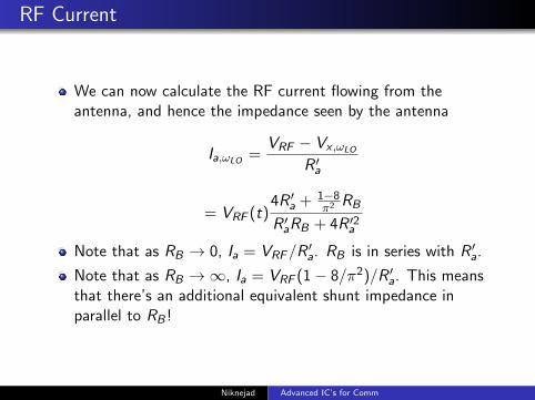
RF Current
We can now calculate the RF current flowing from theantenna, and hence the impedance seen by the antenna
Ia,ωLO=
VRF − Vx ,ωLO
R ′a
= VRF (t)4R ′a + 1−8
π2 RB
R ′aRB + 4R ′2a
Note that as RB → 0, Ia = VRF/R′a. RB is in series with R ′a.
Note that as RB →∞, Ia = VRF (1− 8/π2)/R ′a. This meansthat there’s an additional equivalent shunt impedance inparallel to RB !
Niknejad Advanced IC’s for Comm

Mixer LTI Equivalent Circuit3094 IEEE TRANSACTIONS ON CIRCUITS AND SYSTEMS—I: REGULAR PAPERS, VOL. 57, NO. 12, DECEMBER 2010
Fig. 2. Approximation of waveform from Fig. 1.
capacitors of the mixer and the input on the antenna. Becausethe virtual voltage at in Fig. 1(c) is always short-circuited toone of the output capacitors, it can be described by a stair-stepwaveform (shown in Fig. 2) with four phases correspondingto the four phases of the LO, and with a voltage at each phasecorresponding to one of the output capacitors.
In order to characterize the effective impedance seen by theantenna, we find the current flowing out of the antenna into thereceiver. In the time domain this will be
(5)
We will now look for the impedance seen by the antenna fora near-zero-IF system, where . To find weextract the component of that resides at this frequency usinga Fourier series representation of the signal over a period of time
, and extract the fundamental term. Substituting (4) into thewaveform (shown in Fig. 2) yields a term for the fundamentalat
(6)
from which we can compute
(7)
The current described in (7) looks like the inputtransformed by a combination of and . Several obser-vations can be made from (7). The first is that as ,
, implying that acts in series with .The second is that as , ,implying that there is additional antenna-dependent shunting inparallel with . This leads us to introduce the time-invariantmodel in Fig. 3 for the original time-varying circuit in Fig. 1.This circuit accounts for the linear time-varying (LTV) effectsof the switches with an impedance transform term actingon , and an additional resistance , in shunt with thebaseband resistance . emerges from the charge balancein (3). However, as we will show in Section III-A, in factrepresents power lost due to upconversion by harmonics of theLO through the switches to the antenna.
Given the model in Fig. 3 we can write a simple expressionfor its current
(8)
Fig. 3. LTI equivalent circuit for passive mixer with due to harmonics andimpedance-transformed .
Fig. 4. Simulated and analytical equivalent input impedance versus sweptbaseband resistor .
To find the values for the scaling factor and the virtual shuntresistance , we set the current in our LTV circuit (7) equalto the current for our LTI model (8)
(9)
(10)
Note that while is proportional to in (10), this only holdsas long as is constant across all frequencies, once this ceasesto be true, a more complex description is required, as exploredin Section V.
B. Consequence: Impedance Matching
This model for the passive mixer shows that the impedanceseen by the antenna through a quadrature passive mixer consistsof the parallel combination of and in series with theswitch resistance . Specifically, this impedance becomes
(11)
This result indicates that the impedance seen at the antenna in-terface can be modified by changing . In particular, (11)shows that changing baseband resistance can be used to tunethe input resistance over a range that is limited by the prop-erties of the mixer
(12)
We have confirmed this impedance analysis using numer-ical circuit simulation (PSS and PSP analyses in SpectreRF)of Fig. 1, with NMOS transistors as the switches. We choosetransistor dimensions such that , and choose
, , , and. As can be seen in Fig. 4, sweeping from to
and applying (11) analytically predicts numerical, peri-odic steady-state simulations with high accuracy. The resultingcurve shows that for very high values of , the effectiveconverges to near , and that for very low values of ,
The first R ′a term is obvious, but the next two terms are notat all obvious.
The term γRB is the baseband equivalent resistance seen bythe antenna.
The Rsh term is in shunt and represents additional power loss.It will be shown that this is actually the power loss due to theharmonics of the harmonics of the LO. Up to now it wasderived using charge balance but if we go through eachharmonic and calculate it’s loss as seen from the input port,we arrive at the same result.
Niknejad Advanced IC’s for Comm

Equivalent Circuit Elements
From the model we can calculate the equivalent impedance
Ia(ωLO) = VRF (ωLO)γRB + Rsh
R ′aγRB + R ′aRsh + RshγRB
Equate this to the expression derived from charge balance toget
γ =2
π2≈ 0.203
Rsh = R ′a4γ
1− 4γ≈ 4.3R ′a
Note that Rsh was derived assuming R ′a is constant over allfrequencies, which is not a good assumption for mostantennas or filters that may precede the antenna.
Niknejad Advanced IC’s for Comm

Impedance Matching
Given that the input impedance has a real part that dependson the switch resistance (naturally) but also on the basebandimpedance, we can turn the baseband impedance to realize amatch
Rin = Rsw + γRB ||Rsh
Rsw < Rin < Rsw + Rsh
We’d like to make Rsw � Ra but we’ll return to this pointlater. For now, solve for RB
RB =1
γ
RswRa − RswRsh
Rsw + Rsh − Ra
Niknejad Advanced IC’s for Comm

Antenna Impedance Variation
In the above charge balance derivation, it was assumed thatthe antenna impedance was constant, even at LO harmonics.Since the voltage Vx has harmonics of the LO, the currentdraw from the antenna at these harmonics will differ. If wewrite Vx as a Fourier series and account for the antennaimpedance variation by defining
R ′a(nωLO) = Ra(nωLO) + Rsw
Then the current through the switches is given by
Ia(t) =VRF (t)
R ′a(ωLO)−
∞∑n=1,3,···
Vx ,n(t)
R ′a(nωLO)
Invoking charge balance, we arrive at
Rsh =
∞∑n=3,···
1
n2R ′a(nωLO)
−1
Niknejad Advanced IC’s for Comm

Rsh Harmonic Interpretation
We now have an alternative expression for Rsh
Rsh =
∞∑n=3,5,···
1
n2R ′a(nωLO)
−1
Let’s verify that this agrees with our earlier calculation whenRa is constant
Rsh =
∞∑n=3,5,···
1
n2(Ra + Rsw )
−1
Rsh =
((π2
8− 1
)1
(Ra + Rsw )
)−1
= R ′a4γ
1− 4γ
Niknejad Advanced IC’s for Comm

Non-Zero IF
Excite the circuit with a frequency above or below the LO (toproduce a non-zero IF)
VRF (t) = A cos((ωLO + ωIF )t)
Assume baseband impedance is an RC but excited at non-zero
ZB(ωIF ) = RB ||1
jωIFCL=
RB
1 + jωIFCLRB
Repeating the math and assuming ωIF � ωLO , an essentiallyidentical expression is derived (now with ZB):
Vx(ωRF ) = VRF (ωRF )8
π2
ZB
ZB + 4R ′a
Niknejad Advanced IC’s for Comm

General LTI ModelANDREWS AND MOLNAR: IMPLICATIONS OF PASSIVE MIXER TRANSPARENCY 3097
Fig. 6. New LTI equivalent circuit for frequency-dependent .
, we find an expression becomes essentially identicalto (6)
(28)
This then produces the same derivation of the current asshown above.
If we now reintroduce the LTI model with a simple transfor-mation from to (see Fig. 6), we can rewrite the ex-pression for impedance seen by the antenna (11), including thefrequency-dependent .
(29)
Fig. 7 shows the effective real and imaginary components ofthe impedance seen at IF and at RF due to the frequency-depen-dent components. The presence of the baseband capacitorhas two notable effects on the tunable impedance presented tothe antenna port. First, because the capacitor shunts high-fre-quency IF signals on the baseband port, it creates a band passfilter. As a result, the effect of tuning on the impedancematch diminishes for larger baseband frequencies as be-comes dominated by and ultimately approaches forlarger offset frequencies. The presence of this band pass filterhas been shown to contribute to the attenuation of out-of-bandblockers resulting in measurements of [1],[18]. Second, the imaginary component of looks negativefor positive and positive for negative . This means thatfor a negative IF, the antenna port sees a complex conjugateof the impedance presented by the baseband. Meanwhile, theasymmetric imaginary component of accounts for the fre-quency offset of the ideal match in Fig. 5. This imaginary com-ponent is interacting with the capacitive parasitics on the RFport of the mixer, such that an ideal complex conjugate matchoccurs at a slight frequency offset from the LO.
IV. NOISE PERFORMANCE
A. Noise Performance of Passive Mixer
The time-invariant model in Fig. 3 also simplifies the calcu-lation of the noise contributions for the mixer. To see this, wefirst need to look at the various sources of noise in the circuitshown in Fig. 1. There are three fundamental sources of noise:the baseband resistance , the switch resistance, , and thethermal noise from the antenna itself, . As before, we cansafely merge the antenna and switch resistance into a single re-sistor, . To find the total noise, we compute the total noisecurrent injected into the baseband node, and multiply this withthe total impedance at that node. Thus, if is a real resistor,this current will be: .
Fig. 7. Effective real and imaginary components of as a function of RFfrequency.
Similarly the noise from is . However,to be complete, this noise must also include noise down-con-verted by the mixer at odd harmonics of the LO, such that
. The schematic on the leftside of Fig. 8 shows this model. However, we note that the sumof the antenna noise currents for ,etc., is exactly the noise that would be generated by if itwas a real resistor. Therefore we can use the two noise modelsin Fig. 8 interchangeably. The total noise voltage is the sum ofthe thermal voltage sources corresponding to each resistor inthe circuit. The noise factor for this circuit is found by dividingthe total output noise by the portion of that noise caused by theinput noise of
(30)
If we assume impedance matching to and a switch resis-tance of , this results in . Note that this noiseis dominated by contributions from the baseband resistorand includes no noise from subsequent amplifiers. In the nextsection we will demonstrate how this noise contribution can beminimized in the implementation of an actual receiver using thepassive mixer-first architecture.
B. Receiver Architecture
In order to add gain to the receiver and to improve its noisefigure, all while maintaining the impedance matching function-ality through the passive mixer, we have proposed the receiverarchitecture shown in Fig. 10 [1]. This receiver consists of a pas-sive quadrature mixer, followed by baseband amplifiers in re-
Given the above result, it’s now easy to show that theantenna port is loaded by an impedance given by
Zin(ωIF ) = Rsw +γRB ||Rsh
1 + jωIFCLγRB ||Rsh
From the RF port, this is transformed into a bandpasscharacteristic similar to what we have seen before (due tomixer transparency, a baseband low-pass is converted into abandpass response).
Niknejad Advanced IC’s for Comm

Noise Model3098 IEEE TRANSACTIONS ON CIRCUITS AND SYSTEMS—I: REGULAR PAPERS, VOL. 57, NO. 12, DECEMBER 2010
Fig. 8. Equivalent noise models for LTI model from Fig. 3.
Fig. 9. Equivalent baseband amplifier noise models.
Fig. 10. Proposed passive-mixer first receiver with resistive feedbackamplifiers.
sistive feedback. We find the new effective present on eachbranch by applying the Miller effect to the feedback resistor :
(31)
Substituting the new into the impedance matching LTImodel shows that we can perform impedance matching usingthe amplifier feedback resistors.
Once we have added the feedback amplifiers to implement, the noise performance changes as well. Whereas most of
the noise sources in (30) can be treated as standard resistivethermal noise, the baseband noise is now due to the feedbackresistor and the input referred noise of the amplifier itself[Fig. 9(a)]. This noise is traditionally modeled by a pair ofcorrelated noise sources: a series voltage and shunt current[Fig. 9(b)]. This is equivalent to two voltage sources, as shownon the right of Fig. 9(c).
These two sources both depend upon the input referredvoltage noise of the amplifier, and so are correlated. However,the source present in shunt also depends upon the feedbackresistor and amplifier gain, and can be computed to be
(32)
Substituting the equation for thermal noise and (32) into (30),and accounting for both in the baseband noise (by multiplying
Fig. 11. Simulated and analytical noise figure versus feedback resistor .
the squared noise by ) and in the baseband resistance (by mul-tiplying by ), yields the following noise factor:
(33)
We have verified this relationship (see Fig. 11) with simu-lation using periodic steady state analysis in SpectreRF, with
, , , and the samedevice parameters as in Fig. 4. The simulation results match ana-lyitical predictions well.
By making baseband gain (and so ) large, and biasingthe amplifier with sufficient current to make small, thelatter terms can be made small. Furthermore, by choosing tran-sistor dimensions such that the switch resistance and thereforeits noise are small relative to , we find a limit on the noisefactor which depends on
(34)
For constant , where (10) holds, (34) implies that, or . In cases where antenna impedance
decreases with frequency, this limit is degraded. More gener-ally, Provided that , , and ,all of these terms will be much less than one except the final
Given that this is an LTV system, we must account for all thenoise folding that occurs from every harmonic of the LO. It isfortunate that this can be simply modeled by an equivalentRsh. In fact, we have already derived that Rsh models thepower loss due to the harmonics, so this is not completelysurprising
With this insight, we have a very simple LTI model.
Niknejad Advanced IC’s for Comm

Noise Analysis
Each noise term is summed to calculate the total outputnoise. This expression is then converted to a NF bynormalizing to the source noise
F = 1 +Rsw
Ra+
Rsh
Ra
(Ra + Rsw
Rsh
)2
+RB
Ra
(Ra + Rsw
γZB
)2
In practice, the baseband resistance is realized as a shuntfeedback resistance with an amplifier. In this situation, thebaseband amplifier contributes noise
F =1 +Rsw
Ra+
Rsh
Ra
(Ra + Rsw
Rsh
)2
+γRF
Ra
(Ra + Rsw
γRF
)2
+
γv2a
4kTRa
(Ra + Rsw
γRF+
Ra + Rsw + Rsh
Rsh
)2
Niknejad Advanced IC’s for Comm

Noise Optimization
Zsh should be maximized to minimize contributions ofharmonics to noise and loss.
Zin = Rsh + γZB ||Zsh
Also, this will maximize the tuning range of the system (byvarying RB).
But note that maximizing Zsh requires one to maximize theantenna impedance at the harmonics of the LO, opposite toan LC tank or a resonant antenna.
Niknejad Advanced IC’s for Comm

Optimum Switch Size
Since the switch adds parasitic capacitance in parallel to Zsh,we cannot arbitrarily make the switch large.
Za(ω)→ 0 at ω →∞
Z ′a(ω)→ Rsw for ω →∞Reducing Rsw reduces Zsh at higher frequencies, whichincreases the noise! There’s an intermediate width for optimalperformance.
If we have a very high Q antenna such that the antennaimpedance is zero at harmonics, then Rsh = 4.3Rsw and so
F = 1 +Rsw
Ra+
(Ra + Rsw )2(1− 4γ)
4γRaRsw
For Fmin ≥ 4.05 dB, choose Rsw
Rsw = Ra
√1− 4γ
Niknejad Advanced IC’s for Comm
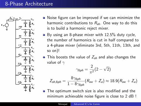
8-Phase Architecture
3100 IEEE TRANSACTIONS ON CIRCUITS AND SYSTEMS—I: REGULAR PAPERS, VOL. 57, NO. 12, DECEMBER 2010
Fig. 13. Positive and negative complex feedback applied to the basebandamplifier.
Fig. 14. Simulated Smith chart for varying .
When this signal is down-converted through the I and Q pathsof the mixer, assuming the two paths are perfectly balanced, weshould get
(39)
We then look at the amplitude of the current present at the in-puts of the amplifiers due to the new cross-connected feedbackresistors we see
(40)
Equation (40) shows that the cross-channel feedback connec-tions introduce a scaled 90 out of phase component ofback to the input. When these currents are back upconverted tothe antenna port, we find
(41)
Using (41) we may write an expression for the effective complexbaseband impedance, , where the sign of the imaginary termdepends on whether the feedback is connected in positive ornegative complex feedback (see Fig. 13)
(42)
Fig. 15. Simulated for varying showing shift in center frequencyof optimal match.
Fig. 16. Eight-phase passive mixer.
Note that if we repeat this analysis for the case where, we find that because of the relative phases of sin
and cos, we actually need to flip the polarity of the feedbackresistors from the Q channel to the I channel, in order to get thesame equivalent complex phase shift. This result is seen in theschematic in Fig. 13.
Using a similar simulation setup to Fig. 5, Fig. 14 shows anSmith-chart of the sweeps of both the real feedback resistorand the complex feedback resistor . This figure demon-
strates the distinct complex nature of the impedance presentedto the antenna port using complex feedback. The sweep using
alone shows some complex impedance due to the parasiticcapacitances present on the switches.
Fig. 15 shows an plot of sweeps of frequency for varyingcomplex feedback resistor . Here we have chosen the valueof from Fig. 5 which provided the best match to .However as we noted earlier, this match was narrowband andcentered around 497 MHz. Fig. 15 shows that complex feed-back can change this center frequency to either side of the LOby interacting with the imaginary component of the antenna
Noise figure can be improved if we can minimize theharmonic contributions to Rsh. One way to do thisis to build a harmonic reject mixer.
By using an 8-phase mixer with 12.5% duty cycle,the number of harmonics is cut in half compared toa 4-phase mixer (eliminate 3rd, 5th, 11th, 13th, andso on)!
This boosts the value of Zsh and also changes thevalue of γ
γ8ph =2
π2(2−
√2)
Zsh,8ph =8γ8ph
1− 8γ8ph(Rsw + Za) ≈ 18.9(Rsw + Za)
The optimum switch size is also modified and theminimum achievable noise figure is close to 2 dB !
Niknejad Advanced IC’s for Comm

References
Weldon Jeffrey Arthur Weldon, High Performance CMOS Transmitters for Wireless Communications, Ph.D.Dissertation, 2005.
Cook B.W. Cook, A. D. Berny, A. Molnar, S. Lanzisera, K.S.J. Pister, “An Ultra-Low Power 2.4GHz RFTransceiver for Wireless Sensor Networks in 0.13/spl mu/m CMOS with 400mV Supply and an IntegratedPassive RX Front-End,” IEEE Internationa Solid-State Circuits Conference(ISSCC), Digest of TechnicalPapers, pp.1460,1469, 6-9 Feb. 2006.
Molnar A. Molnar, B. Lu, S. Lanzisera, B.W. Cook, K.S.J. Pister, “An ultra-low power 900 MHz RF transceiver forwireless sensor networks,” Custom Integrated Circuits Conference, 2004. Proceedings of the IEEE 2004 ,vol., no., pp.401,404, 3-6 Oct. 2004.
AndrewsTCAS C. Andrews and A. Molnar, “Implications of Passive Mixer Transparency for Impedance Matching andNoise Figure in Passive Mixer-First Receivers,” IEEE Trans. on. Circuits and Systems-I: Regular Papers,vol. 57, no. 12, Dec. 2010.
AndrewsJSSC C. Andrews and A. Molnar, “A Passive Mixer-First Receiver With Digitally Controlled and Widely TunableRF Interface,” IEEE J. of Solid-State Circuits, vol. 45, no. 12, Dec. 2010.
Niknejad Advanced IC’s for Comm