an overview of substrate noise reduction techniquescdr/pubs/substrate_isqed_2004.pdf · an overview...
TRANSCRIPT

An Overview of Substrate Noise Reduction Techniques
Shahab Ardalan, and Manoj Sachdev [email protected], [email protected]
Department of Electrical and Computer Engineering University of Waterloo
200 University Avenue West Waterloo, Ontario, Canada N2L 3G1
Abstract This paper provides an overview of the recent circuit level and physical level substrate noise reduction techniques. Several of these techniques are compared for their advantages and disadvantages in “System-on-Chip” applications.1. Introduction As “System-on-Chip” designs are becoming popular, the substrate noise topic has attracted much attention in the past [2-5,8,17-19]. Even today, a significant research effort is devoted to mitigate the impact of mostly digitally generated substrate noise on sensitive mixed-signal circuits [1,7,9-16]. In mixed-signal circuits, complex and noisy digital circuits are integrated on the same substrate with noise-sensitive analog circuits. In fact, with heavily integrated mixed signal ICs becoming ever so common, it is possible for the noise-induced currents injected into the common substrate, to result in functional failures of the analog and digital blocks.From designers’ perspective, one would like to find circuit and physical level techniques to protect sensitive circuits from substrate noise effects. In this article, we have divided substrate noise reduction techniques into (i) circuit, and (ii) physical levels. Rest of the paper is organized as follows, in the following section, an overview of circuit techniques is provided. Section 3 is devoted to physical level considerations to reduce the impact of substrate noise. In Section 4, conclusions are drawn. 2. Circuit Level ConsiderationA wide variety of circuit techniques are available to (i) reduce the occurrence of the substrate noise, (ii) design circuits that have higher degree of immunity to substrate noise, and (iii) cancel the generated substrate noise. 2. 1. Differential versus Single-Ended Circuits Differential circuits are often preferred to single-ended circuits in noisy environments. In differential circuits, the substrate noise appears as a common-mode signal on the differential output. Therefore, the impact of substrate noise in differential output is several orders of magnitude smaller than single ended output. It is often difficult to measure the substrate noise directly. Hence, its severity is often determined through its impact on various circuit parameters. For example, in phase-lockedloops (PLLs) the impact of substrate noise generated in voltage-controlled oscillator (VCO) manifests as the jitter at the output of the PLL [1]. In this study, authors investigated
single and differential ring oscillators, shown in Fig.1, for their substrate noise sensitivities.
(a) (b) Fig.1: (a) Single-ended Ring Oscillator, (b): Differential Ring Oscillator
Fig.2 shows cycle jitter and cycle-to-cycle jitter of (a) the single-ended ring oscillator and (b) the differential ring oscillator [1]. The single-ended ring oscillator has approximately 10x higher jitter compared to differential ring oscillator caused by the substrate noise.
(a) (b) Fig.2: Cycle Jitter and Cycle-to-Cycle Jitter of (a) the Single-ended Ring
Oscillator and (b) the Differential Ring Oscillator [1].
Fig.3: Jitter of the 3-stage and the 6-stage of the Differential Ring Oscillator
Similarly, Fig.3 depicts the jitter of three-stage and six-stage oscillator designed for a frequency of 500MHz with constant tail current and voltage swings. We observe that the minimum values of cycle jitter and cycle-to-cycle jitter are
0-7695-2093-6/04 $20.00 2004 IEEE
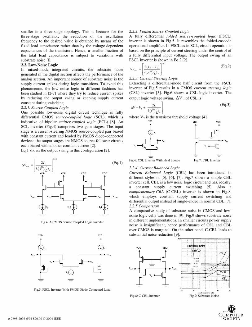
smaller in a three-stage topology. This is because for the three-stage oscillator, the reduction of the oscillation frequency to the desired value is obtained by means of the fixed load capacitance rather than by the voltage-dependent capacitances of the transistors. Hence, a smaller fraction of the total load capacitance is subject to variations with substrate noise [l]. 2.2. Low-Noise Logic In mixed-mode integrated circuits, the substrate noise generated in the digital section affects the performance of the analog section. An important source of substrate noise is the supply current spikes during logic transitions. To avoid this phenomenon, the low noise logic in different fashions has been studied in [2-7] where they try to reduce current spikes by reducing the output swing or keeping supply current constant during switching. 2.2.1. Source-Coupled Logic One possible low-noise digital circuit technique is fully differential CMOS source-coupled logic (SCL), which is indicative of bipolar emitter-coupled logic (ECL) [8]. An SCL inverter (Fig.4) comprises two gain stages: The input stage is a current-steering NMOS source-coupled pair biased with constant current and loaded by PMOS diode–connected devices; the output stages are NMOS source-follower circuits each biased with another constant current [2]. Eq.1 shows the output swing in this configuration [2].
2/1
1
)(
2
′=∆
pp
out
LWk
IV
(Eq.1)
Fig.4: A CMOS Source Coupled Logic Inverter
Fig.5: FSCL Inverter With PMOS Diode-Connected Load
2.2.2. Folded Source-Coupled Logic A fully differential folded source-coupled logic (FSCL) inverter is shown in Fig.5. It resembles the folded-cascode operational amplifier. In FSCL as in SCL, circuit operation is based on the principle of current steering under the control of a fully differential input voltage. The output swing of an FSCL inverter is shown in Eq.2 [2].
2/1
12
)(
)(2
′−
=∆pp
out
LWk
IIV
(Eq.2)
2.2.3. Current Steering Logic Extracting a differential-mode half circuit from the FSCL inverter of Fig.5 results in a CMOS current steering logic (CSL) inverter [3]. Fig.6 shows a CSL logic inverter. The output logic voltage swing, V∆ , of CSL is
′+≈∆
nn
T
LWk
IVV
)(
2 1 (Eq.3)
where VT is the transistor threshold voltage [4].
Fig.6: CSL Inverter With Ideal Source Fig.7: CBL Inverter
2.2.4. Current Balanced Logic Current Balanced Logic (CBL) has been introduced in different styles in [5], [6], [7]. Fig.7 shows a simple CBL inverter cell. CBL is a low noise logic circuit and has, ideally, a constant supply current switching [5]. Also a complementary-CBL (C-CBL) inverter is shown in Fig.8, which employs constant supply current switching and differential output instead of single-ended in normal CBL [7]. 2.2.5 Comparison A comparative study of substrate noise in CMOS and low-noise logic cells was done in [9]. Fig.9 shows substrate noise in different implementations. In smaller circuits power supply noise is insignificant, hence performance of CSL and CBL over CMOS is marginal. On the other hand, C-CBL leads to substantial noise reduction [9].
Fig.8: C-CBL Inverter Fig.9: Substrate Noise
0-7695-2093-6/04 $20.00 2004 IEEE

2.3. Reduced Supply Bounce CMOS Circuit Circuit techniques can be employed to reduce the digitally generated supply noise affecting larger segment of Vdd. One such implementation, reduced supply bounce (RSB) CMOS logic (Fig.10) was proposed in [10]. Pairs of decoupling capacitors (Cd) and a series resistor (Rd)formed by a linear region MOSFET (Md) are provided locally for VDD/GND paths in every digital block necessary to reduce noise. Dedicated ground wiring is desirable for Cd, but not absolutely necessary. Cd’s serve as local charge reservoirs covering the flat logic transitions within the block and are recharged continuously by the external power supplies with time constants to the degree of RdCd. Thus reduced and decoupled supply bounce causes flattened supply current [11].
Fig.10: RSB-CMOS Circuit Configuration [11].
The efficiency of the RSB-CMOS circuits was demonstrated in [10]. Fig.11 illustrates a comparison between RSB-CMOS with conventional CMOS. From the figure, we can conclude an RSB-CMOS circuit results in more than 90% substrate noise reduction over that of a conventional CMOS.
Fig.11: Substrate Noise Waveforms by Test Circuit [10].
2.4. Active Substrate Noise Reduction Method In [12], the substrate noise reduction was approached using an active method. The approach is to sample the noise at the noise receiver section (analog block) of the mixed-signal design, and then direct this noise into the input stage of a negative feedback loop. After reversing its phase, the noise is re-injected into the substrate. Having the opposite phase of the original noise, the re-injected noise can cancel up to 83% of the noise travelling inside the substrate. Fig.12 shows the circuit model for simulation of the substrate coupling noise with a negative feed back loop, which is realised by a single op-amp. Fig.13 shows the reduction of the digital noise in frequency variation. The data in this figure depict that the measured noise levels were higher (38%) than the simulated values [12].
Fig.12: Circuit Model of Negative Feedback Method
Fig.13: Peak-to-Peak Noise Versus Switching Frequency
2.5. Pin Swapping Method Pin swapping is one of the circuit level methods for noise reduction. This technique optimizes switching noise while maintaining operation speed, power consumption and transistor count. To measure switching noise, monitoring the maximum peak value of dynamic current provided by supply source have been used in [13]. Circuit level simulations of multiple-input gates show that noise generated by switching inputs depends on the specific input considered, due to asymmetry in the implementation of gates (input capacitance, substrate effect, layout, etc). Table.1 shows simulation result for a three-input NAND gate. (Fig.14)
Fig.14: input NAND
Transition in:
a (bc=11) b (ac=11) c (ab=11)
z rises 271.7µA 314.5µA 339.7µA
z falls 293.0µA 293.2µA 299.5µA
Table.1: Supply Current Peak during Transition with Respect to Inputs
Simulated results demonstrate that input transition at a is less noisy than transitions at other inputs. Schematic is first analyzed to obtain noisy nodes. Such information is used for pin swapping optimization. Logic simulation can be carried out to obtain information about simultaneous switching activity in nodes, since simultaneous transitions constitute the main contribution to substrate noise. The analysis of the obtained information is used to detect the situations, through
0-7695-2093-6/04 $20.00 2004 IEEE

checking the nodes with higher activity and mapping such nodes to the less noisy pins in the library cells. It follows that in the optimization process brings in a final optimized schematic for low noise generation [13]. 2.6. Supply Current Shaping Method Supply current waveform shaping is a noise reduction technique based on avoiding large current peaks on the supply lines, e.g., by spreading (otherwise simultaneous) switching events in time or reducing the supply voltage. As a result the frequency spectrum of the supply current is modified as shown in Fig.16: (i) the total spectral power is reduced and (ii) the corner frequency is moved to lower frequencies [14].
(a) (b) Fig.16: (a) Simulated supply current transients with the same time-domain
energy and (b) Resulting substrate noise transients
Reducing the total spectral power of the supply current also reduces the generated substrate noise. The rms value of the substrate noise is proportional to the integral of the power spectrum [14]. Moving the corner frequency of the supply current spectrum below the major resonance frequency in the supply current transfer function will reduce the substrate noise generation significantly since most of the noise power is a result of this resonant behavior [14]. Fig17 shows comparison between normal circuit and clock shaped circuit.
Fig.17: Simulated supply current waveform
3. Physical Level Considerations In this section we describe layout and other physical techniques to reduce the effect of substrate noise. 3.1. Single Guard Ring Guard rings and substrate taps are often used to reduce substrate noise. The layout of a typical guard ring is shown in Fig.18. The ring is a surface-region heavily doped with the majority-carrier dopant and is intended to form a Faraday shield around any sensitive device needs to be protected
against substrate noise. Guard ring provides the lower impedance path to ground compare to other paths for substrate noise.
(a) (b) Fig.18: Guard Ring: (a) Layout, (b) Cross-Section
Often Isolation (Is) between contacts is defined as the ratio of the voltage swing on the receiver contact to the voltage swing on the injector contact. Simulations were carried out in [15] show variation of Is versus distance between guard ring and injector contact. Fig.19 shows example layout and results of simulations are shown in Fig.20. Similarly, Fig.22 shows effect of the guard ring width on isolation when δ equals to 50µm and 100µm [15].
Fig.19: Layout of Guard Ring Example
Fig.20: Simulation Result of Guard Ring Example
3.2. Dual Guard Rings The effect of one guard ring placed around the injector or the receiver was discussed in previous section. It is also possible to place guard rings around both injector and receiver contacts. The Is between two single-ended contacts, with a guard ring placed around each contact is examined in [15]. Fig.21 shows layout of the dual guard ring method and comparison between dual ring and single ring is shown in Table.2 [15].
Fig.21: Dual Guard Ring Layout
0-7695-2093-6/04 $20.00 2004 IEEE

Fig.22: Simulation Result of Guard Ring Example δ = 50µm and δ = 100µm
Table.2: Comparison between Single Guard Ring and Dual Guard Ring
3.3. Buried Substrate Shields The buried substrate shields can be categorized in three major types: 3.3.1. Faraday Shield A highly conductive layer under the switching devices may provide a low-impedance path to ground for the substrate noise. However, if used improperly, this low–impedance path may also cause noise coupling between neighbouring devices [16]. Fig.23 shows layout and cross-section of this method. An experiment done in [16] shows the effectiveness of this method. Results of the test structure are presented in Table.3.
Fig.23: Faraday Shield Layout and Cross-Section
Method With deep contacts
Without deep contacts
Without buried layers N/A 248mVpp
Buried layers only under the digital section
105mVpp 183mVpp
Buried layer only under the analog section
75mVpp 232mVpp
Buried layer under all the circuitry
26mVpp 165mVpp
Table.3: Comparison of the Different Implementations of Buried Layer
3.3.2. Dielectric Shield Dielectric isolation is used in this method to isolate the nodes from substrate. This approach physically increases the impedance between the injector and the receiver by increasing the resistivity of the substrate that surrounds either of the two nodes. This method is implemented in Silicon-On-
Insulator (SOI). In these substrates, bulk silicon is isolated from the thin active surface silicon layer, by means of buried oxide layer. The layout and cross-section of this method is shown in Fig.24. This method provides very good isolation, but it adds to processing costs, since it requires the use of special silicon substrate [15].
Fig.24: Junction Shield Layout and Cross-Section
3.3.3. Junction Shield In this method a buried minority-type of carrier enclosure around the device plays the role of an isolator. Fig.25 shows cross-section and layout of junction shield. Comparison between junction shield and dielectric shield is pointed out in Table.4 and showed in Fig.26 [17].
Fig.25: Junction Shield Layout and Cross-Section
Frequency Dielectric (SOI)
Shield Junction Shield
100 MHz -66 dB -55 dB
200 MHz -54 dB -51 dB
400 MHz -48 dB -46 dB
700 MHz -49 dB -41 dB
1000 MHz -48 dB -37 dB
Table.4: Comparison between Junction Shield and Dielectric Shield
3.4. Forward-Biased Guard Ring A study has verified that by creating a band-pass filter, using the inductance of the bond wire and the capacitance of a forward biased diode, the substrate noise can be reduced [18].Forward-Biased guard ring is shown in Fig.27, where the n+guard ring is connected to the Vbias, which is a negative voltage, through a large resistor. This forward-biased n+p-junction with constant current creates a charge storage region in the diode resulting in a capacitance in the Pico Farad range. These components form a band-pass filter, the resonant-frequency of which depends on diode current and is given by Eq.1:
Ω=
25/..
10
IL τω (Eq.1)
where L is inductance of the bound wire, τ is the transit time and I is diode current [18]. Fig.28 shows substrate noise voltage in two different circuits (a) circuit with forward- biased and (b) circuit without guard ring [19].
Method Frequency Isolation
Without Guard Ring 100MHz / 1GHz -62dB / -34dB
Single Guard Ring 100MHz / 1GHz -99dB / -45dB
Dual Guard Ring 100MHz / 1GHz -130dB/ -57dB
0-7695-2093-6/04 $20.00 2004 IEEE

Fig.26: Simulation Result of Comparison between Junction Shield and Dielectric Shield Done by Medici
Fig.27: Model of Forward-Biased Guard Ring
Fig.28: Effectiveness of Forward-Biased Guard Circuit
4. Conclusion Integration of digital and analog building blocks on the same substrate has resulted in undesirable levels of substrate noise in contemporary “System-on-Chip” devices. Different injection and reception mechanisms caused by a variety of effects may induce noisy currents into the substrate. These effects can be modeled and verified experimentally by researchers. The complexity and precision of the model depends on the application or the employed circuit. A class of the techniques in this regard, takes into account circuit design considerations to reduce the occurrence of substrate noise in the system, while other techniques try to stop or eliminate the noise propagation through physical level techniques. Alternatively, active noise cancellation/filtering techniques can be employed to reduce the impact of substrate noise on sensitive mixed-signal blocks.
5. References [1] F. Herzel et al., “A Study of Oscillator Jitter Due to Supply and Substrate Noise,” IEEE Trans. on CAS-II: Analog and Digital Signal Processing, vol. 46, pp. 56-62, Jan. 1999. [2] D. J. Allstot et al., “Folded Source-Coupled Logic vs. CMOS Static Logic for Low-Noise Mixed-Signal ICs,” IEEE Trans. on CAS-I: Fundamental theory and applications, vol. 40, pp. 55530, Sep. 1993. [3] D. J. Allstot et al., “Analog Logic Techniques Steer Around the Noise,” IEEE Circuits and Devices Magazine, Vol. 9, pp. 18-21, Sep. 1993. [4] H. Ng et al., “CMOS Current Steering Logic for Low-Voltage Mixed-Signal Integrated Circuits,” IEEE Trans. on VLSI Systems, vol. 5, pp. 301-308, Sep. 1997. [5] E. Albuquerque et al., “NMOS Current-balanced Logic,” IEE Electronics Letters, vol. 32, pp. 997-998, May 1996. [6] E. Albuquerque et al., “Current-Balanced Logic for Mixed Signal IC’s,” Proc. of the IEEE International Symposium on Circuit and System, pp. I.274-I.277, 1999. [7] E. Albuquerque et al., “A New Low-Noise Logic Family for Mixed-Signal Integrated Circuits,” IEEE Trans. on CAS-I Fundamental theory and applications, vol. 46, pp. 1498-1500, Dec. 1999. [8] J. Lohstroh et al., “Devices and Circuits for Bipolar (V) LSI,” IEEE Proc.,Vol. 69, pp. 812-826, Jul. 1981. [9]E. Albuquerque et al., “Evaluation of Substrate Noise in CMOS and Low-Noise Logic Cells,” Proc. of the IEEE International Symposium on Circuit and System, pp. VI.750-VI.753, 2001. [10] M. Nagata et al., “Reduced Substrate Noise Digital Design for Improving Embedded Analog Performance,” Proc. of IEEE International Solid State Circuit Conference, Digest of Technical Papers, pp. 224–225, 2000. [11] M. Nagata et al., “Physical Design Guides for Substrate Noise Reduction in CMOS Digital Circuits,” IEEE Journal of Solid State Circuits, Vol. 36, pp. 539-549, Mar. 2001. [12] T. Liu et al., “Active Substrate Coupling Noise Reduction Method for ICs,” IEE Electronics Letters, vol. 35, pp.1631634, Sep. 1999. [13] P. Parra, “ Reduction of Switching Noise in Digital CMOS Circuits by Pin Swapping of Library Cells,” Proc. of International Workshop-Power And Timing Modeling, Optimization and Simulation (PATMOS), 2001. [14] M. Badaroglu et al., “Methodology and Experimental Verification for Substrate Noise Reduction in CMOS Mixed-Signal ICs with Synchronous Digital Circuits,” IEEE Journal of Solid State Circuits, Vol. 37, pp. 1381395, Nov. 2002. [15] E. Charbon et al., “Substrate Noise Analysis and Optimization for IC Design,” Kluwer Academic Publishers, 2001. [16] X. Aragones, et al., “Analysis and Solution for Switching Noise Coupling in Mixed-Signal ICs,” Kluwer Academic Publishers, 1999. [17] K. Joardar, ”Signal Isolation in BiCMOS Mixed Mode Integrated Circuits,” IEEE Proc. of the Bipolar/BiCMOS Circuits and Technology Meeting, pp.178-181, 1995.[18] L. Forbes et al., “Resonant Forward-biased Guard-ring Diodes for Suppression of Substrate Noise in Mixed-mode CMOS Circuits,” IEE Electronics Letters, vol. 31, pp. 720-721, Apr. 1995. [19] L. Forbes et al., “Guard ring Diodes for Suppression of Substrate Noise and Improved Reliability in Mixed-mode CMOS Circuits,” Proc. of International Symposium on the Physical and Failure Analysis of Integrated Circuits, pp.145-148, 1995.
0-7695-2093-6/04 $20.00 2004 IEEE