analog spiking neuromorphic circuits and systems …
TRANSCRIPT
ANALOG SPIKING NEUROMORPHIC CIRCUITS AND SYSTEMS FOR
BRAIN- AND NANOTECHNOLOGY-INSPIRED COGNITIVE
COMPUTING
by
Xinyu Wu
A dissertation
submitted in partial fulfillment
of the requirements for the degree of
Doctor of Philosophy in Electrical and Computer Engineering
Boise State University
December 2016

© 2016
Xinyu Wu
ALL RIGHTS RESERVED
BOISE STATE UNIVERSITY GRADUATE COLLEGE
DEFENSE COMMITTEE AND FINAL READING APPROVALS
of the dissertation submitted by
Xinyu Wu
Dissertation Title: Analog Spiking Neuromorphic Circuits and Systems for Brain- and
Nanotechnology-Inspired Cognitive Computing
Date of Oral Examination: 2 November 2016
The following individuals read and discussed the dissertation submitted by student Xinyu
Wu, and they evaluated his presentation and response to questions during the final oral
examination. They found that the student passed the oral examination.
John Chiasson, Ph.D. Co-Chair, Supervisory Committee
Vishal Saxena, Ph.D. Co-Chair, Supervisory Committee
Hao Chen, Ph.D. Member, Supervisory Committee
Hai Li, Ph.D. External Examiner
The final reading approval of the dissertation was granted by Vishal Saxena, Ph.D., Co-
Chair of the Supervisory Committee. The dissertation was approved by the Graduate
College.
iv
ABSTRACT
Human society is now facing grand challenges to satisfy the growing demand for
computing power, at the same time, sustain energy consumption. By the end of CMOS
technology scaling, innovations are required to tackle the challenges in a radically different
way. Inspired by the emerging understanding of the computing occurring in a brain and
nanotechnology-enabled biological plausible synaptic plasticity, neuromorphic computing
architectures are being investigated. Such a neuromorphic chip that combines CMOS
analog spiking neurons and nanoscale resistive random-access memory (RRAM) using as
electronics synapses can provide massive neural network parallelism, high density and
online learning capability, and hence, paves the path towards a promising solution to future
energy-efficient real-time computing systems. However, existing silicon neuron
approaches are designed to faithfully reproduce biological neuron dynamics, and hence
they are incompatible with the RRAM synapses, or require extensive peripheral circuitry
to modulate a synapse, and are thus deficient in learning capability. As a result, they
eliminate most of the density advantages gained by the adoption of nanoscale devices, and
fail to realize a functional computing system.
This dissertation describes novel hardware architectures and neuron circuit designs
that synergistically assemble the fundamental and significant elements for brain-inspired
computing. Versatile CMOS spiking neurons that combine integrate-and-fire, passive

v
dense RRAM synapses drive capability, dynamic biasing for adaptive power consumption,
in situ spike-timing dependent plasticity (STDP) and competitive learning in compact
integrated circuit modules are presented. Real-world pattern learning and recognition tasks
using the proposed architecture were demonstrated with circuit-level simulations. A test
chip was implemented and fabricated to verify the proposed CMOS neuron and hardware
architecture, and the subsequent chip measurement results successfully proved the idea.
The work described in this dissertation realizes a key building block for large-scale
integration of spiking neural network hardware, and then, serves as a step-stone for the
building of next-generation energy-efficient brain-inspired cognitive computing systems.
vi
TABLE OF CONTENTS
Abstract .............................................................................................................................. iv
List of Tables ..................................................................................................................... xi
List of Figures ................................................................................................................... xii
List of Abbreviations ....................................................................................................... xxi
List of Publication .......................................................................................................... xxiii
Chapter 1 Introduction .........................................................................................................1
Grand Challenges and Rebooting Computing .........................................................3
Human Society Desires a Continued Growing Computing Capability .......3
New Ways Are Required to Tackle Unstructured Big Data ........................4
Unsustainable Energy for Sustainable Computing Capability Growth .......5
The End of Semiconductor Transistor Scaling ............................................6
Von Neumann Bottleneck ............................................................................8
Brain and Nanotechnology-Inspired Neuromorphic Computing ...........................10
This Dissertation ....................................................................................................13
Chapter 2 Brain Inspiration for Computing .......................................................................15
A Big Picture of Neuron Properties .......................................................................15
Neuron Morphology...................................................................................15
Neuron Electrical Properties ......................................................................17

vii
Synapse ......................................................................................................19
Neuron Models.......................................................................................................22
McCulloch-Pitts Model ..............................................................................22
Leaky Integrate-and-Fire Model ................................................................23
Hodgkin and Huxley Model.......................................................................25
Izhikevich Model .......................................................................................26
Brain-Inspired Learning .........................................................................................27
Hebbian Learning.......................................................................................27
Spike Timing Dependent Plasticity ...........................................................29
Associative Learning .................................................................................31
Competitive Learning ................................................................................32
Brain-Inspired Architectures ..................................................................................35
Perceptron ..................................................................................................35
Multi-Level Perceptron ..............................................................................35
Recurrent Networks ...................................................................................37
Hierarchical Models and Deep Neural Networks ......................................38
Summary ................................................................................................................42
Chapter 3 Nanotechnology for Neuromorphic Computing ...............................................44
Overview of Emerging Memory Technologies .....................................................45
Phase Change Memory (PCM) ..............................................................................47
Spin-Transfer-Torque Random-Access-Memory (STT-RAM) .............................50
Resistive Random-Access-Memory (RRAM) .......................................................51
Resistance Switching Modes .....................................................................52
viii
Switching Mechanisms and Operation ......................................................54
STDP in Bipolar Switching RRAMs .........................................................58
Device Characteristics for Neuromorphic Computing ..........................................64
Energy Efficiency ......................................................................................64
Device Dimensions ....................................................................................65
Resolution ..................................................................................................65
Retention and Endurance ...........................................................................66
Crossbar and 3D Integration ..................................................................................67
Summary ................................................................................................................70
Chapter 4 Introduction to Building Blocks of Analog Spiking Neurons ...........................71
Spatio-Temporal Integration ..................................................................................71
Passive Integrators .....................................................................................73
Opamp Integrators .....................................................................................76
Threshold and Firing Functionality .......................................................................80
Spike Shaping ........................................................................................................82
Spike-Frequency Adaptation and Adaptive Thresholds ........................................84
Axons and Dendritic Trees ....................................................................................87
Summary ................................................................................................................87
Chapter 5 A CMOS Spiking Neuron for Dense RESISTIVE Synapses and in Situ STDP
Learning .............................................................................................................................89
Accommodating RRAM Synapses ........................................................................90
The Neuron Design ................................................................................................93
Reconfigurable Architecture and Dual-Mode Operation ...........................95
Opamp and Dynamic Biasing ....................................................................97
ix
Asynchronous Comparator ........................................................................99
Phase Controller .......................................................................................100
Spike Generator ......................................................................................101
Circuit Simulations ..............................................................................................103
Opamp Characterizations .........................................................................103
Integration, Firing and Leaking ...............................................................103
Spike Shaping ..........................................................................................109
Power Consumption .................................................................................110
Single Post-Synaptic Neuron System ..................................................................112
In Situ STDP Learning .............................................................................113
Example of Associative Learning ............................................................117
Chip Implementation ...........................................................................................121
Design environment .................................................................................122
Neurons ....................................................................................................122
RRAM Arrays ..........................................................................................124
Tunability .................................................................................................124
Other modules ..........................................................................................126
Chip Measurements .............................................................................................127
Measurement Setup ..................................................................................128
Spiking Behaviors ....................................................................................129
Experiments of Associative Learning ......................................................133
Summary ..............................................................................................................135
Chapter 6 Generalized CMOS Spiking Neuron and Hybrid CMOS / RRAM Integration
for Brain-Inspired Learning .............................................................................................136
x
Enabling Brain-Inspired Learning .......................................................................136
Revisiting the Reconfigrable Architecture ...........................................................139
Triple-Mode Operation ........................................................................................141
Hybrid CMOS / RRAM Neuromorphic Systems ................................................144
Single Layer Neural Network with Crossbar Architecture ..................................145
Example of Supervised Handwriting Digits Recognition ....................................146
The Application of Optical Character Recognition .................................146
Simulation Setups ....................................................................................146
Simulation Results ...................................................................................149
Discussions ..............................................................................................151
Summary ..............................................................................................................157
Chapter 7 Conclusion and Outlook ..................................................................................159
Contributions........................................................................................................159
Discussions and Future Work ..............................................................................161
References ........................................................................................................................165

xi
LIST OF TABLES
Table 3.1 Performance Metrics of Memory Devices as Synapses.....................................67
Table 5.1 Comparison of Several Neuron Designs ..........................................................112
Table 5.2 Tunable parameters of the neuron output spike waveform ..............................126
Table 5.3 Measured Parameters of the Typical Neuron Output Spike ............................131
xii
LIST OF FIGURES
Figure 2.1. Diagram of three neuron cells. (A) A cortical pyramidal cell. These are the
primary excitatory neurons of the cerebral cortex. (B) A Purkinje cell of
the cerebellum. Purkinje cell has an elaborate dendritic tree which can
form up to 200,000 synaptic connections. (C) A stellate cell of the cerebral
cortex. Stellate cells one of a large class of inter-neurons that provide
inhibitory input the neurons of the cerebral cortex. (Adapted from [64]). 16
Figure 2.2. Spatio-temporal summation and action potential generation. (A) No
summation: Excitatory stimuli E1 separated in time do not add together on
membrane potential. (B) Temporal summation: two excitatory stimuli E1
close in time add together on membrane potential. (C) Spatial summation:
two simultaneous stimuli E1 and E2 at different locations add together
membrane potential. (D) Spatial summation of excitatory and inhibitory
inputs can cancel each other out on membrane potential. (Adapted from
[57])............................................................................................................18
Figure 2.3. Synaptic transmission at chemical synapses. (A) An action potential arriving
at a pre-synaptic axon causes voltage-gated Ca2+ channels at the active
zone to open. (B) A high concentration of Ca2+ near the active zone causes
vesicles containing neurotransmitter to fuse with the pre-synaptic cell
membrane and release their contents into the synaptic cleft. (C)
Neurotransmitter molecules diffuse across the synaptic cleft and bind
specific receptors on the post-synaptic membrane. These receptors cause
ion channels to open (or close), thereby changing the membrane
conductance and membrane potential of the post-synaptic cell. (Adapted
from [59]). ..................................................................................................20
Figure 2.4 A leaky integrate-and-fire neuron response under a time-varying input current.
(Top) a raster plot of the discrete output spike train of which the action
potential dynamics is ignored. (Middle) Membrane voltage Vmem with the
action potentials overlaid onto it as vertical lines. (Bottom) Trace of the
input current. (Adapted from [64]). ...........................................................24
Figure 2.5. The Izhikevich model is capable of mimicking a number of different neuron
behaviors that have been experimentally observed. (Adapted from [62]). 26
xiii
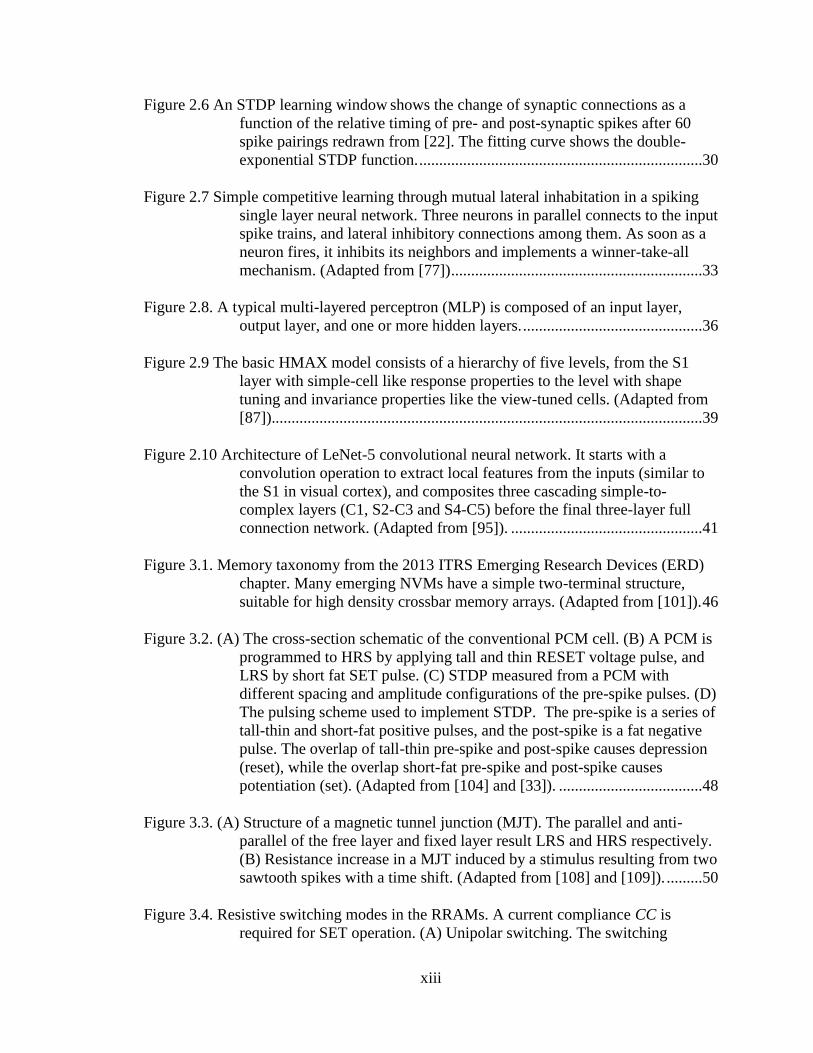
Figure 2.6 An STDP learning window shows the change of synaptic connections as a
function of the relative timing of pre- and post-synaptic spikes after 60
spike pairings redrawn from [22]. The fitting curve shows the double-
exponential STDP function. .......................................................................30
Figure 2.7 Simple competitive learning through mutual lateral inhabitation in a spiking
single layer neural network. Three neurons in parallel connects to the input
spike trains, and lateral inhibitory connections among them. As soon as a
neuron fires, it inhibits its neighbors and implements a winner-take-all
mechanism. (Adapted from [77]) ...............................................................33
Figure 2.8. A typical multi-layered perceptron (MLP) is composed of an input layer,
output layer, and one or more hidden layers. .............................................36
Figure 2.9 The basic HMAX model consists of a hierarchy of five levels, from the S1
layer with simple-cell like response properties to the level with shape
tuning and invariance properties like the view-tuned cells. (Adapted from
[87])............................................................................................................39
Figure 2.10 Architecture of LeNet-5 convolutional neural network. It starts with a
convolution operation to extract local features from the inputs (similar to
the S1 in visual cortex), and composites three cascading simple-to-
complex layers (C1, S2-C3 and S4-C5) before the final three-layer full
connection network. (Adapted from [95]). ................................................41
Figure 3.1. Memory taxonomy from the 2013 ITRS Emerging Research Devices (ERD)
chapter. Many emerging NVMs have a simple two-terminal structure,
suitable for high density crossbar memory arrays. (Adapted from [101]). 46
Figure 3.2. (A) The cross-section schematic of the conventional PCM cell. (B) A PCM is
programmed to HRS by applying tall and thin RESET voltage pulse, and
LRS by short fat SET pulse. (C) STDP measured from a PCM with
different spacing and amplitude configurations of the pre-spike pulses. (D)
The pulsing scheme used to implement STDP. The pre-spike is a series of
tall-thin and short-fat positive pulses, and the post-spike is a fat negative
pulse. The overlap of tall-thin pre-spike and post-spike causes depression
(reset), while the overlap short-fat pre-spike and post-spike causes
potentiation (set). (Adapted from [104] and [33]). ....................................48
Figure 3.3. (A) Structure of a magnetic tunnel junction (MJT). The parallel and anti-
parallel of the free layer and fixed layer result LRS and HRS respectively.
(B) Resistance increase in a MJT induced by a stimulus resulting from two
sawtooth spikes with a time shift. (Adapted from [108] and [109]). .........50
Figure 3.4. Resistive switching modes in the RRAMs. A current compliance CC is
required for SET operation. (A) Unipolar switching. The switching
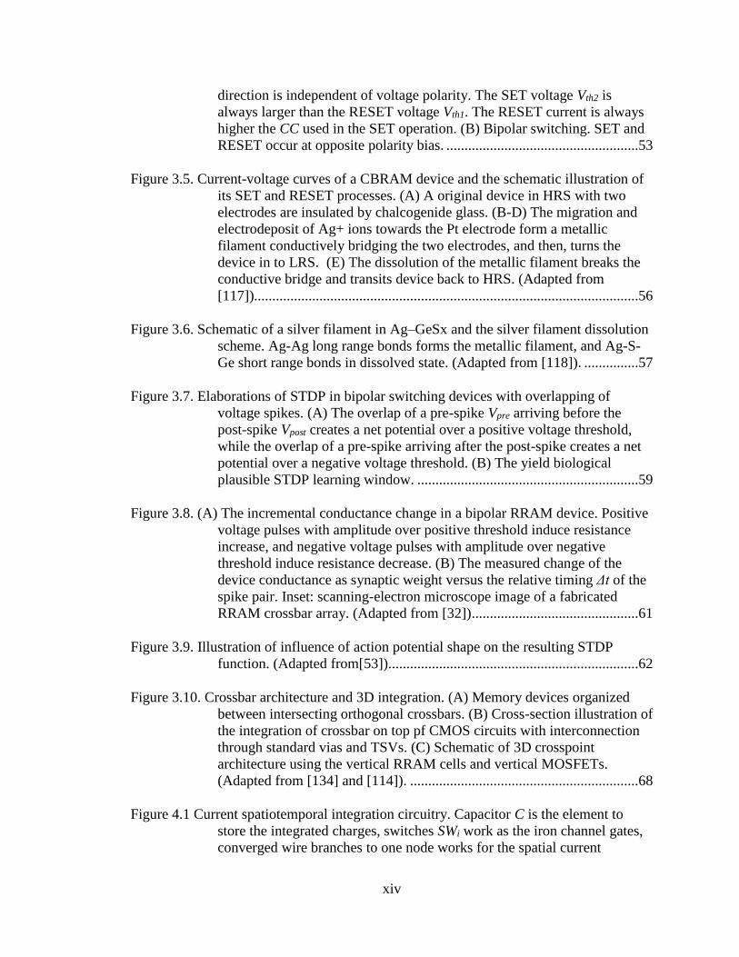
xiv
direction is independent of voltage polarity. The SET voltage Vth2 is
always larger than the RESET voltage Vth1. The RESET current is always
higher the CC used in the SET operation. (B) Bipolar switching. SET and
RESET occur at opposite polarity bias. .....................................................53
Figure 3.5. Current-voltage curves of a CBRAM device and the schematic illustration of
its SET and RESET processes. (A) A original device in HRS with two
electrodes are insulated by chalcogenide glass. (B-D) The migration and
electrodeposit of Ag+ ions towards the Pt electrode form a metallic
filament conductively bridging the two electrodes, and then, turns the
device in to LRS. (E) The dissolution of the metallic filament breaks the
conductive bridge and transits device back to HRS. (Adapted from
[117])..........................................................................................................56
Figure 3.6. Schematic of a silver filament in Ag–GeSx and the silver filament dissolution
scheme. Ag-Ag long range bonds forms the metallic filament, and Ag-S-
Ge short range bonds in dissolved state. (Adapted from [118]). ...............57
Figure 3.7. Elaborations of STDP in bipolar switching devices with overlapping of
voltage spikes. (A) The overlap of a pre-spike Vpre arriving before the
post-spike Vpost creates a net potential over a positive voltage threshold,
while the overlap of a pre-spike arriving after the post-spike creates a net
potential over a negative voltage threshold. (B) The yield biological
plausible STDP learning window. .............................................................59
Figure 3.8. (A) The incremental conductance change in a bipolar RRAM device. Positive
voltage pulses with amplitude over positive threshold induce resistance
increase, and negative voltage pulses with amplitude over negative
threshold induce resistance decrease. (B) The measured change of the
device conductance as synaptic weight versus the relative timing Δt of the
spike pair. Inset: scanning-electron microscope image of a fabricated
RRAM crossbar array. (Adapted from [32]) ..............................................61
Figure 3.9. Illustration of influence of action potential shape on the resulting STDP
function. (Adapted from[53]).....................................................................62
Figure 3.10. Crossbar architecture and 3D integration. (A) Memory devices organized
between intersecting orthogonal crossbars. (B) Cross-section illustration of
the integration of crossbar on top pf CMOS circuits with interconnection
through standard vias and TSVs. (C) Schematic of 3D crosspoint
architecture using the vertical RRAM cells and vertical MOSFETs.
(Adapted from [134] and [114]). ...............................................................68
Figure 4.1 Current spatiotemporal integration circuitry. Capacitor C is the element to
store the integrated charges, switches SWi work as the iron channel gates,
converged wire branches to one node works for the spatial current

xv
summation, and temporal factor comes from time-dependence of current
sources Ii. ...................................................................................................72
Figure 4.2 Simple MOSFET-capacitor follower-integrator. Single MOSFET is used as
the voltage controlled current source, and input spikes applied on the gate
of the MOSFET works as a switching signal.............................................74
Figure 4.3 Log-domain integrator circuits. (A) “Tau-cell” circuit; (B) Current mirror
integrator; (C) Differential-pair integrator. (Adapted from [146]). ...........75
Figure 4.4 Opamp based active inverting integrator circuit. Capacitor C connected
between the negative input port and output port of the opamp forms a
negative feedback, and makes X a node of virtual ground. Current Iin
flowing into X turns to charge C with a same amount current If and yields
Vc, while the potential at X remains constant. ............................................77
Figure 4.5 Response of opamp-based inverting integrator. These pulses cause step
decrease and increase to the output voltage Vout. The step size is linearly
proportional to the amount of current, and the direction of change depends
on the current flow direction. The effect of current aggregation occurs
when spikes Vin1 and Vin2 overlap. The current summing node potential VX
remains constant during the integration. ....................................................79
Figure 4.6 Axon-hillock circuit. (A) Schematic diagram; (B) membrane voltage and
output voltage traces over time. (Adapted from [146]). ............................81
Figure 4.7 A neuron circuit comprises circuits for both setting explicit spiking thresholds
and implementing an explicit refractory period. (A) Schematic diagram;
(B) Membrane voltage trace over time. (Adapted from [153]). ................82
Figure 4.8 Spike-frequency adaptation is a silicon neuron. (A) SFA is implemented by
subtracting charges from the integration capacitor with a PMOS current
source controlling by the neuron’s spiking output. (B) The instantaneous
firing rate as a function of spike count. The inset shows how the individual
spikes increase their inter-spike interval with time. (Adapted from
[154])..........................................................................................................85
Figure 4.9 A possible circuitry for realizing adaptive firing threshold. A voltage
comparator is employed for explicit threshold crossing detection. Each
time the neuron fires, an output controlled current source Iadp charges
capacitor Cadp and increases Vthr from the baseline value Vthr0; when no
firing occurs, parallel resistor Radp discharges Cadp towards Vthr0. .............86
Figure 5.1 Block diagram of the proposed event-driven leaky integrate and fire neuron
circuit. It includes integrate-and-fire, STDP-compatible spike generation,
xvi
large current driving ability and dynamic powering in a compact circuit
topology with a reconfigurable architecture based on a single opamp. .....94
Figure 5.2 Dual-mode operation. (A) Integration mode: opamp is configred as a leaky
integrator to sum the currents injected into the neuron. Voltages of Vrest are
held for both pre- and post-resistive syanpses. (B) Firing mode: opamp is
reconfigured as a voltage buffer to drive resisitive synapses with STDP
spikes in both forward and backward directions. Noting backward driving
occurs at the same node (circled) of current summing which enables in-
situ learning in bare synapses. ...................................................................96
Figure 5.3. A circuit implementation of the opamp with the dynamic biasing. A split
class-AB driver is embedded in a compact folded-cascode topology. The
major branch on the right side (red in dark area) provides large current
driving capability; while the minor low-power branch in the middle (blue)
works with the first stage to provide the desired gain. The complementary
signals Φint and Φfire are used to activate the major branch only during the
firing mode. ................................................................................................98
Figure 5.4. Circuits schematics of a compact asynchronous comparator. The positive
feedback is incorporated with cross-connected coupled network to
enhance the gain of the source-coupled differential pair. ........................100
Figure 5.5. Control and phase generation circuitry. The four non-overlapping phase
signals control the operational mode of the neuron and define the timings
of output spike waveform. .......................................................................101
Figure 5.6. STDP-compatible spike generation. (A) A spike with a short narrow positive
pulse of large amplitude followed by a longer slowly exponentially
decreasing negative tail, and (B) the respective circuit realization. ........102
Figure 5.7 Testing circuitry used to characterize CMOS spiking neuron. Three resistors
are connected to the neuron input and convert three spiking inputs into
currents. ....................................................................................................104
Figure 5.8 Response of membrane voltage Vmem and typical output firing spikes Vspk with
interleaving input spikes and equal strength synapses. It shows the linear
inverting integration of identical input currents from three spike sources,
while each of the input spike led to a moving down step on the membrane
voltage Vmem. Once Vmem ran across the 200 mV firing threshold, a spike
with waveform customized for STDP learning was generated. ...............105
Figure 5.9 Response of membrane voltage Vmem and typical output firing spikes Vspk with
interleave input spikes and three different strength synapses. Here R1 = 50
kΩ, R2 = 100 kΩ, and R3 = 200 kΩ make the three input synapses have 2×,
1× and 0.5× strength. The respective input trains, in red, green and blue,
xvii
yield 100 mV, 50mV and 25mV steps to membrane voltage Vmem
respectively. .............................................................................................106
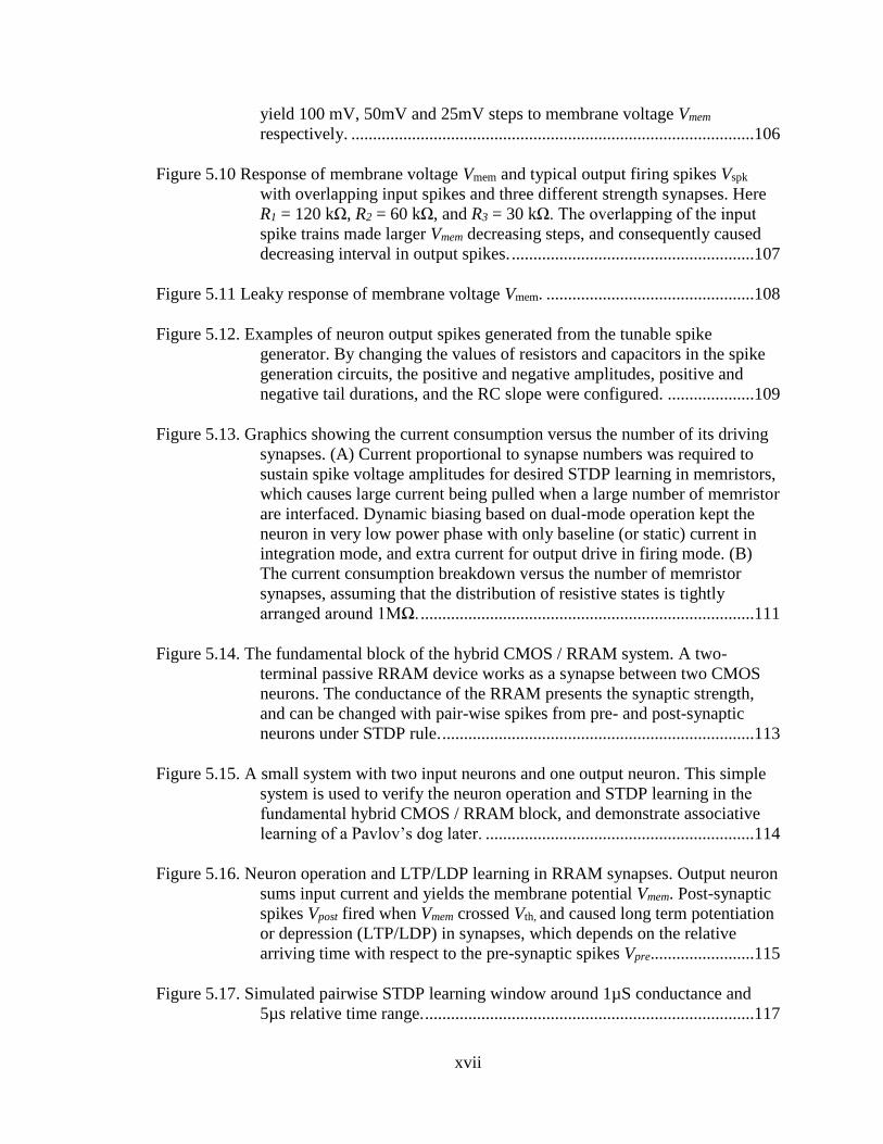
Figure 5.10 Response of membrane voltage Vmem and typical output firing spikes Vspk
with overlapping input spikes and three different strength synapses. Here
R1 = 120 kΩ, R2 = 60 kΩ, and R3 = 30 kΩ. The overlapping of the input
spike trains made larger Vmem decreasing steps, and consequently caused
decreasing interval in output spikes. ........................................................107
Figure 5.11 Leaky response of membrane voltage Vmem. ................................................108
Figure 5.12. Examples of neuron output spikes generated from the tunable spike
generator. By changing the values of resistors and capacitors in the spike
generation circuits, the positive and negative amplitudes, positive and
negative tail durations, and the RC slope were configured. ....................109
Figure 5.13. Graphics showing the current consumption versus the number of its driving
synapses. (A) Current proportional to synapse numbers was required to
sustain spike voltage amplitudes for desired STDP learning in memristors,
which causes large current being pulled when a large number of memristor
are interfaced. Dynamic biasing based on dual-mode operation kept the
neuron in very low power phase with only baseline (or static) current in
integration mode, and extra current for output drive in firing mode. (B)
The current consumption breakdown versus the number of memristor
synapses, assuming that the distribution of resistive states is tightly
arranged around 1MΩ. .............................................................................111
Figure 5.14. The fundamental block of the hybrid CMOS / RRAM system. A two-
terminal passive RRAM device works as a synapse between two CMOS
neurons. The conductance of the RRAM presents the synaptic strength,
and can be changed with pair-wise spikes from pre- and post-synaptic
neurons under STDP rule. ........................................................................113
Figure 5.15. A small system with two input neurons and one output neuron. This simple
system is used to verify the neuron operation and STDP learning in the
fundamental hybrid CMOS / RRAM block, and demonstrate associative
learning of a Pavlov’s dog later. ..............................................................114
Figure 5.16. Neuron operation and LTP/LDP learning in RRAM synapses. Output neuron
sums input current and yields the membrane potential Vmem. Post-synaptic
spikes Vpost fired when Vmem crossed Vth, and caused long term potentiation
or depression (LTP/LDP) in synapses, which depends on the relative
arriving time with respect to the pre-synaptic spikes Vpre........................115
Figure 5.17. Simulated pairwise STDP learning window around 1µS conductance and
5µs relative time range. ............................................................................117
xviii
Figure 5.18 Development of an associative learning simulated in a hybrid CMOS /
memristor Pavlov’s dog. ..........................................................................118
Figure 5.19 Resistance evolution of the two memristor synapses in associative learning
simulation. ................................................................................................119
Figure 5.20 Zoom-in view of the spike trains of the three CMOS neurons (top panel), net
potential across memristors with peak voltage exceeded threshold Vth,p of
the memristor (middle panel), and synaptic potentiating in the two
memristor synapses (bottom panel) during associative learning
simulation. ................................................................................................120
Figure 5.21 An example of RRAM crossbar layout. The fifth metal layer (green) of CMOS
chip was used to layout bottom electrodes and alignment masks, and
tungsten vias were used as contact points to plant RRAM devices between
the bottom electrodes and top electrodes (red, not on CMOS chip but will be
processed in BEOL). ................................................................................123
Figure 5.22 Layouts of (A) current steer W-2W ladder and (B) 4×4 common centroid
structure MIM capacitor bank. ..................................................................125
Figure 5.23 Test chip layout. Three neurons and three 8×8 bottom electrodes of RRAM
crossbar were integrated on a single chip. A big glass opening area was
reserved for BEOL processing. Several individual contact points were
designed with various sizes to enable on-chip RRAM devices tests. ......127
Figure 5.24 Micrograph of the test chip in 180nm CMOS. N1, N2 and N3 are three
silicon neurons. Biasing is biasing and voltage reference circuitries, and
Digital I/F is the digital interface. ............................................................128
Figure 5.25 Setup for test chip measurements. A FPGA was used to communicate with
the chip and configure the neuron parameters (e.g. spike shape, threshold,
trimming…). Two arbitrary waveform generators were employed to
provide the original input stimulation to the neurons. IFN3 was connected
to the outputs of IFN1 and IFN2 through two resistors to form a small
network. ...................................................................................................129
Figure 5.26 Measured spikes from single neuron. (A) a measured spike train, and (B) the
zoom-in shows a typical neuron output spike with a positive tail and ramp
up negative tail. ........................................................................................130
Figure 5.27 The over-threshold net potential across resistive synapse created by a STDP
spike pair from pre- and post-synaptic neurons. ......................................132
Figure 5.28 An experimental demonstration of associative leaning using the fabricated
chip. By simultaneously applying stimulations to both IFN1 and IFN2,
xix
synapse R2 was strengthened with STDP learning, which carried larger
currents with spike and caused IFN3 responded to IFN2 inputs
independently after learning. ...................................................................134
Figure 6.1. Two inhibitory connection schemes. (A) One-to-one scheme. Each neuron has
an inhibitory connection to another neuron in the local group. (B) Shared
bus. All neurons in the local group share a common inhibitory bus. .......137
Figure 6.2. Detailed circuit schematic of the WTA bus interface. A potential firing event
triggers the D-flip-flop to read into the WTA bus status. When there is no
spike event on the bus Vwtab, the tri-state gate is enabled to generate the
firing signal Φfire. On the other hand, when there is a spike event on the
bus, a discharging signal Φd is generated. ...............................................138
Figure 6.3. Diagram of the proposed leaky IFN. It includes integrate-and-fire, WTA
interface, STDP-compatible spike generation, large current driving ability
and dynamic powering in a compact circuit topology with a reconfigurable
architecture based on a single opamp. .....................................................140
Figure 6.4. Tri-mode operation of the proposed leaky integrate-and-fire neuron (A)
Integration mode: The opamp is configured as a negative integrator to sum
current on Cmem causing the membrane potential Vmem to move down until
its crosses a firing threshold voltage Vthr. Without an input current,
voltages at the two inputs of the opamp are held at Vrest. Post-synapses are
disconnected from the neuron. (B) Firing mode: phase signals Φint, Φfire,
Φ1 and Φ2 control the spike generator to create a STDP-compatible spike
Vspk which is buffered and driven by the opamp. Then, the spike
propagates in both backward and forward directions to pre-synapses and
post-synapses respectively. The activation of either Vcpr or Vtch causes a
firing event, which is also presented on the WTA bus by pulling-up the
bus with Vwtab. (C) Inhibitive discharge mode: Φd is active to discharge the
Cmem when an active Vwtab signal is detected on the WTA bus. The opamp
is configured as a low-power buffer with Φint is active and Φfire is inactive.
Also, the neuron is isolated from the post-synapses. ...............................143
Figure 6.5. A single layer of hybrid CMOS / RRAM neuromorphic computing system.
The RRAM synapses are organized in crossbar, input and output CMOS
spiking neurons sit on the two sides of the crossbar, and local WTA buses
connecting a group of neurons for competitive learning. ........................145
Figure 6.6. A spiking neural system for the pattern recognition application of optical
character recognition (OCR). ...................................................................147
Figure 6.7. Examples of digits from UCI optical handwriting dataset. ...........................148
xx
Figure 6.8. Direct plot of memristor conductance learned in a circuit-level simulation
with 4 output neurons during one epoch of training. ...............................152
Figure 6.9 Conductance evolution rearranged as 8×8 bitmap. Before training, all synapses
were initialized with a Gaussian random distributed conductance (μ =
8.5nS, σ = 4nS). After training, the maximum conductance is 53μS, and
the minimum conductance is 6.6 nS. With the training moving on, the
memristor network extracted distinctive features of digits: loop of the digit
“0”, the vertical line of the “1”, or the bone of “2” and “7”. ...................152
Figure 6.10. Test results of the neural network with an input spike train composed of 20
samples for each digit and presented in class-by-class fashion. Without
learning, a random synaptic network caused decision neurons spiking
arbitrarily. After learning, each of these 4 output neurons is mostly
selective to one of the 4 classes and spiking in the same class-by-class
fashion of input. .......................................................................................153
Figure 6.11 In a test case with one digit presented to the system, total current flowing into
decision neurons were separated due to the modulation of synaptic
network, which caused different integration speeds. The neuron with the
largest input current I0 had its membrane voltage Vmem0 cross the firing
threshold Vth first, and then won the competition of the race-to-fire
first. ..........................................................................................................154
Figure 6.12 Firing opportunity and spike outputs of 4 output neurons. All neurons have
almost equal opportunities to spiking at the beginning. After learning, their
spiking probabilities are modulated by their synaptic connections and
distinguished. As result, a winner emerges. .............................................154

xxi
LIST OF ABBREVIATIONS
ANN Artificial Neural Network
BEOL Back-End-Of-The-Line
CBRAM Conductive-Bridging Random-Access Memory
CMOS Complementary Metal–Oxide–Semiconductor
CNN Convolutional Neural Network
CPU Central Processing Unit
DNN Deep Neural Network
HRS High Resistance State
IC Integrated Circuit
IFN Integrate-and-Fire Neuron
IT Information Technology
LIF Leaky Integrate and Fire
LRS Low Resistance State
LTP / D Long-Term Potentiation / Depression
MLP Multi-Layer Perceptron
MOSFET Metal–Oxide–Semiconductor Field-Effect Transistor
NMOS N-channel MOSFET
NVM Non-Volatile Memory
xxii
Opamp Operational Amplifier
PCM Phase Change Memory
PMOS P-channel MOSFET
RRAM Resistive Random-Access Memory
SNN Spiking Neural Network
STDP Spike-Timing Dependent Plasticity
STT-RAM Spin-Transfer-Torque Random-Access Memory
VLSI Very-Large-Scale Integration
WTA Winner-Take-All
xxiii
LIST OF PUBLICATION
1. Xinyu Wu and Vishal Saxena, “Synergy of CMOS neurons with bistable RRAM
synapses enabling bio-plausible stochastic STDP”, IEEE International Electron
Devices Meeting (IEDM), 2016, in review.
2. Vishal Saxena, Xinyu Wu, and Maria Mitkova. "Addressing challenges in
neuromorphic computing with memristive synapses.", Neuromorphic Computing
Workshop: Architectures, Models, and Applications, 2016.
3. Xinyu Wu, Vishal Saxena, Kehan Zhu, and Sakkarapani Balagopal. "A CMOS spiking
neuron for brain-inspired neural networks with resistive synapses and in situ learning."
IEEE Transactions on Circuits and Systems II: Express Briefs 62, no. 11 (2015): 1088-
1092.
4. Xinyu Wu, Vishal Saxena, and Kehan Zhu. "Homogeneous spiking neuromorphic
system for real-world pattern recognition." IEEE Journal on Emerging and Selected
Topics in Circuits and Systems 5.2 (2015): 254-266.
5. Xinyu Wu, Vishal Saxena, and Kehan Zhu. "A CMOS spiking neuron for dense
memristor-synapse connectivity for brain-inspired computing." IEEE International
Joint Conference on Neural Networks (IJCNN), 2015.
6. Xinyu Wu, Vishal Saxena, and Kristy A. Campbell. "Energy-efficient STDP-based
learning circuits with memristor synapses." SPIE Sensing Technology+ Applications,
2014.
7. Sakkarapani Balagopal, Kehan Zhu, Xinyu Wu and Vishal Saxena, “Design-to-testing:
a low-power, 1.25 GHz, single-bit single-loop continuous-time Δ Σ modulator with 15
MHz bandwidth and 60 dB dynamic range”, Analog Integrated Circuits and Signal
Processing, 2016, in press.
8. Kehan Zhu, Vishal Saxena and Xinyu Wu, “Modeling and Optimization of the Bond-
Wire Interface in a Hybrid CMOS-Photonic Traveling-Wave MZM Transmitter”, IEEE
International System-on-Chip Conference (SOCC), 2016, in press.
9. Kehan Zhu, Vishal Saxena, Xinyu Wu, and Wan Kuang. "Design considerations for
traveling-wave modulator-based CMOS photonic transmitters." IEEE Transactions on
Circuits and Systems II: Express Briefs62, no. 4 (2015): 412-416.
10. Kehan Zhu, Vishal Saxena, and Xinyu Wu. "A comprehensive design approach for a
MZM based PAM-4 silicon photonic transmitter." IEEE International Midwest
Symposium on Circuits and Systems (MWSCAS), 2015.

xxiv
11. Kehan Zhu, Vishal Saxena, Xinyu Wu, and Sakkarapani Balagopal. "Design analysis
of a 12.5 GHz PLL in 130 nm SiGe BiCMOS process." IEEE Workshop on
Microelectronics and Electron Devices (WMED), 2015.

1
CHAPTER 1
INTRODUCTION
The brain is an amazing and mysterious organ. It is the computational and mission
control center that drives the whole operation of the body. Although brains vary between
small clusters of neurons to the enormous and astonishingly complex brains of mammals
and human being, they engage with the world in a stunningly effective and efficient way.
For example, honeybees recognize various colors, remember routes up to seven miles, and
communicate with each other using the their unique "waggle" dance language while
foraging for nectar. The human brain can perform perception, visual, sound, smell, touch
object recognition, language translation and fine-motor skills with trivial effort even
without a conscious mind involved in the task. The honeybee achieves its remarkable
learning, navigation and cognitive work with a tiny brain which has one million neurons in
a cubic millimeter size and burn less than a milliwatt of power, while a human brain is a
three-pound weight self-operation “wet” machine operating with only 20 to 30 watts.
Modern autonomous robots and electronics computers can do some of these tasks
but require several orders of magnitude higher space and energy, as well as need
customized programming. For example, a rough-terrain quadruped robot carried onboard
computers operating in hundreds watts to manage the sensors, control the robot behavior
and travel with pre-defined global positioning system routes [1]; a self-teaching artificial
2
intelligence system learned to recognize cats and human faces in 200×200 video clips after
watching 10 million images using a datacenter cluster with 16,000 central processing unit
(CPU) cores [2] with an estimated power consumption of 300 kilowatts; and a neural
simulation on a supercomputer simulated the cat’s brain with 109 neurons and 1013
synapses at 700 times slower than real-time while burning about 2 megawatts [3].
Although animal brains outperform modern computers in many aspects, the
mainstream computing machines in past half-century were created based on the
architecture drafted by John von Neumann in 1943 [4]. This architecture is characterized
by separating program and data memory from arithmetic and logical computations. A CPU
fetches instructions and operands from memory, performs sequential computations, and
returns results to memory. In the same year, McCulloch and Pitts proposed a neuro-inspired
computing model, which described a neuron into a mathematical weight summing and
thresholding function [5]. Although, a two-layer artificial neural network (ANN) capable
of learning certain classifications by adjusting connection weights was implemented based
on this neuron model by Rosenblatt in 1958 [6], ANN-based computing were fall far behind
von Neumann computers on main stage of commuting technology after the inventions at
Bell Labs of transistor in 1947, integrated circuits (ICs) in 1958 by Jack Kilby and 1959
by Robert Noyce.
The invention of transistors allows the switching and amplification of electronic
currents. Further, the engineering breakthrough of ICs fuels a lot of transistors to be put on
less than stamp-size semiconductor chips. They sparked and steamed the following 50
years’ consumer, computing and communication technology revolutions and greatly
shaped today’s human society. In fact, the technology supporting the von Neumann

3
computing architecture has greatly evolved. Since 1970’s, with the adoption of
complementary metal–oxide–semiconductor (CMOS) technology, the size of silicon
transistors was dramatically and continuously scaled down without jeopardizing power
consumption. This resulted in the number of transistors in a IC doubling approximately
every 18 months, which is known as Moore’s law, and an era of very-large-scale
integration (VLSI). The transistor scaling down endows an exponential increase in
computing performance which fulfilled human society’s demand for computing power.
This fulfilment was made possible largely because transistors have the unusual quality of
getting better as they get smaller; a small transistor can be turned on and off with less power
and at greater speeds than a larger one. This meant that one could use more and faster
transistors without needing more power, and thus that chips could get bigger as well as
better [7].
The von Neumann architecture has been powering nearly all computing systems
from home appliance microcontroller, mobile phone, home PC, internet infrastructure to
supercomputers to date due to its ease of programming and intuitive operation. However,
this engine that powered the past decades’ information technology (IT) revolution is losing
its steam due to its essential constraints, many upcoming fundamental physical limitations
and new emerging problems with the demand for radically different computation.
Grand Challenges and Rebooting Computing
Human Society Desires a Continued Growing Computing Capability
Current human society endeavors have been transformed as computer system
capability by its exponential performance ascending since 1970s. Faster computers create

4
not just the ability to do old things faster but the ability to do new things that were not
feasible at all before [8]. Increasing computer performance has powered the whole IT
revolution, greatly accelerated the pace of scientific discoveries and has rooted deeply in
our daily lives.
People enjoy faster response from their personal computers (PC), mobile phones,
media players, and navigation devices; people expect always-connected instant chatting,
faster internet search and smooth online video streaming which is powered by more
computing capability in datacenters; Engineers and scientists desire higher speed
workstations and supercomputers to accelerate the pace of their theoretical and
experimental discoveries; other high-performance computing fields include whole brain
neural network simulation, public and national security, climate change, structure of
proteins, understanding life cycle of stars, functions of living cells, behavior of subatomic
particles, economics, high-energy physics, and nuclear weapons.
New Ways Are Required to Tackle Unstructured Big Data
After human society entered PC era, the ways to store and process information have
been greatly changed. Based on this increasing variety of digital electronics devices,
information is generated from different sources, such as PC, digital camera, digital audio
recorders and many more. In spite of their different forms and characteristics, all the
information is more and more saved in the format of digital data. This trend is even more
accelerated along with the popularity of mobile devices, video surveillance, remote
sensing, and Internet of Things. Data created from social media posting, email, office
document processing, sensors, medical imaging instrument, machine logging, public
recording, DNA sequencing and cosmic exploring, is growing in an unprecedented pace.

5
Every minute, there are 400 hours of new video uploaded to YouTube [9]; Every day in
the future, square kilometer array, a radio telescope to be built for cosmic studies will
generate up to 1020 bits [10]. More than 90% of these new generated data is and will be in
an unstructured fashion [11] — meaning these human and machine generated textual data
is fundamentally deferent from the data that stored in conventional database management
system with keys, records, attributes, and indexes, and can be managed and analyzed with
conventional computing system. Data will be valuable only if it can be analyzed — new
ways is required to extract meaning out of it, then we can make inroads in improving
business plan, making new discoveries, reducing fraud, ferreting out waste, and even
confirming acts of terror. The capability of analyzing large unstructured data will become
a key basis of competition, underpinning new waves of productivity growth, innovation,
and consumer surplus.
Unsustainable Energy for Sustainable Computing Capability Growth
Energy is consumed in all the computing devices everyday around us – from
milliwatt home sensor systems to megawatts supercomputers. In between, a large number
of devices, including media players, wireless routers, mobile phones, tablets, set-top-box,
TV, PC, servers and storage systems, are consuming a few watts to kilowatts. In 2015,
worldwide combined shipments for PCs, tablets, and mobile phones reached 2.4 billion
units [12]. Enabling present human society to do many more things more efficiently and
collaborate across the globe in real-time, the majority of these devices are always-
connected to 24×7 running computing and networking infrastructures. With the exploding
data generated and transferred, the consequent energy consumption is skyrocketing. By
2013, the global IT ecosystem used about 1,500 trillion watt-hours of electricity annually,

6
approaching 10% of global electricity generation [13]. Where, the energy consumption of
a single datacenter or supercomputer can be astronomical number – the most powerful
supercomputer takes 15 megawatts to operate [14]; a latest Facebook datacenter equipped
GPUs as machine learning accelerators needs 84 megawatts backup power [15]; and the
top datacenter consumes 150 megawatts [16]. If no major paradigm shift in the design and
operation of computing systems, the anticipated and growing energy requirements for
future computing needs will hit a wall by 2040 [10] – meaning computing will use all the
energy the human society can produce.
Besides the large-scale energy challenge, high energy-efficient computing is also
urged in space and weight constrained small-scale applications. Distributed sensors have a
potential huge number to perform collective tasks and distributed computing; they also
need on-site intelligence and communication ability that allow decisions and actuation.
Unmanned aerial vehicles like drones have tough requirements on their power supply. The
battery capacity must trade-off with the aerial performance, but more autonomy and
intelligence are required. High-performance computing systems that consumes very low
amounts of power is the solution to meet these twin characteristics. Thus, radical
improvement in the energy efficiency of computing system is needed.
The End of Semiconductor Transistor Scaling
In the last forty years, the semiconductor industry has made amazing progresses in
scaling Complementary Metal-Oxide-Semiconductor (CMOS) transistors. This transistor
scaling is driven by reducing transistor gate length (or feature size) by a scaling factor in
each new CMOS technology generation. To obtain good transistor characteristics, other
dimensional factors, the oxide thicknesses and the gate width also reduced proportionally.
7
As result, more gates can be placed on a chip of roughly the same area and cost as before.
If the supply voltage decreases in a same pace at the same time, the delay of the gate also
decreases in the same pace – meaning switching frequency increases in a same ratio, and
the dynamic power consumption of the transistor decreases in a faster pace (square ratio).
The computational capability of conventional microprocessors was increasing
exponentially under this full scaling trend from 1970s to 1980s. From late 1990s, CMOS
technology started running into some limitations that make it impossible to continue along
that full-scaling path. Accompanied with the scaling down of supply voltage, the transistor
switching threshold voltage was decreased together to maintain the circuit characteristics.
The decreasing of the threshold voltage consequently leads to the increase of subthreshold
leakage current. Subthreshold leakage current contributes to CMOS static power, which
was too small compared to the dynamic power, thus generally was neglected. But
ultimately by the 90-nm node in 2000, the feature size of CMOS transistors became
sufficiently small that the static power dissipation through leakage and parasitic currents
started to became larger than the dynamic power consumption for switching [17]. As a
result, voltage scaling down slowed and the race of increasing CPU clock frequency
stopped. Simulations at the time quickly demonstrated that the continued dimensional
scaling without a concomitant voltage reduction would quickly yield a power density
resulting in temperatures well above the melting points of the metals and even the
semiconductors being used for the systems [18].
Since then, new types of scaling rules as well as new designs and materials were
introduced to reduce the power dissipation. However, MOSFETs have fundamental limits
cannot be overcome even switching to new materials: On and off currents ratio for

8
meaningful switch provides the lower boundary of supply voltage and threshold voltage;
the minimum channel doping for a given supply voltage limits the tolerance of threshold
voltage variance; and a minimum oxide thickness is required to produce a transistor could
reliably work for years [19]. While, the hard physical limitation is the transistor
dimensions. By Aug 2016, the most advanced CMOS technology for CPU has its transistor
gate length is 10nm, which is not far away from the size of the atoms used in silicon chip
fabrication. If Moore’s law continued, the transistor length will meet the size of silicon
atom at 0.2 nm just 8 years later. Finally, cost of chip manufacturing may render continued
scaling infeasible. A state-of-the-art fab for manufacturing microprocessors now costs
around 7 billion US dollars. An estimated cost of the fab for 5 nm chips could rise to over
16 billion US dollars, or nearly a third of Intel’s current annual revenue. In 2015 that
revenue, at 55.4 billion US dollars, was only 2% more than in 2011 [7]. So, from economic
standpoint, the transistor scaling is also ended.
Von Neumann Bottleneck
In the thirty-five years of their history, all computing chips follow the architecture
drafted by von Neumann in 1943, of which program and data memories are separated from
arithmetic and logical computations. Differing with the original von Neumann’s draft that
CPU fetches instructions and data and perform computation in a sequential manner, chip
makers have made many improvements to the chip architecture to satisfy specific data
processing requirements under certain constrains of memory bandwidth and power
consumption in the history of computer development. In 1980’s, digital signal processors
employed data bus in addition to the instruction bus (known as Harvard architecture) and
added parallel accelerators to improve the performance of multiplication-addition
9
computation; in 1990’s, similar ideal applied to graphic processing and yielded GPU with
hundreds and thousands specific computation cores on a single chip. When CPUs ran into
the power wall in middle of 2000’s, chip makers began to include more processor cores on
each die. Ideally, parallelizing all computing tasks, same as the supercomputer does, will
make the computation faster, but this doesn’t help to improve the energy-efficiency and is,
in fact, limited by the interface between processor and memory1. First, the memory latency
is unavoidable in von Neumann architecture. By dividing the system into two big blocks,
memory and processor, the processor uses at least five steps in sequence to perform a
computation: fetch an instruction from memory, decode the instruction, read data from the
memory, execute, and write the result back to the memory. When the data is stored in
external memory – meaning not on the same chip of processor, the data access can be time
consuming. Because the memory improvements have mostly been in density – the ability
to store more data in less space rather than transfer rates, the processor has to wait for data
to be fetched from memory. No matter how fast a processor can work, in effect it is limited
to the rate of transfer allowed by the bottleneck. Despite that modern processors have
integrated on-chip memory (called cache) to ease the challenge, the unstructured data, e.g.
images, generally has big size, needs complicated computation, causes huge data exchange
between processor and memory, thus, cannot be fitted in on-chip caches. Multi-core CPUs
also face the dark silicon issue, where large sections of chips remain unutilized to manage
power and thermal constraints.
In conclusion, the conventional computing platforms cannot last in current growing
path to fulfill the human society’s demand. So, there is a need to create a new type of
1 In precise words, the separation is between computing unit and memory. Processor is used here for simplification purpose. Today’s
processor can have different memories on the chip, and all mainstream CPU/DSP/GPU chips have been integrated memories.
10
computer that can reboot the computing capability to solve unfamiliar problems with a
significant leap in energy efficiency.
Brain and Nanotechnology-Inspired Neuromorphic Computing
Conventional computers are designed for precise arithmetic computational tasks
with structural organized data which primarily originated from needs in national defense
and scientific research, and later widely spread to engineering development, business
operation and personal computing. On the other hand, starting from almost the same time,
early brain-inspired computing techniques are employed in another class of computational
tasks, called pattern recognition, which aim at more analogous computing with
unstructured data, e.g. image classification, text recognition, speed understanding and
language translation. These two classes of computing tasks traditionally exploit a different
set of software tools and techniques, but both run on the same computer hardware
architecture – the von Neumann architecture (there are a few customized hardware for
neural computing but have never been in the mainstream). Recently, with the explosion of
unstructured data and the rising of deep learning techniques, these two computing paths
rapidly converge in almost all the computing areas, from electronic personal assistant,
social networking to financing trading, new material discovery, cosmology research, DNA
sequencing, and national defense. In view of this computing paradigm convergence and
the foreseeable energy challenges, the mysterious wetware architecture of human brains,
which only consume 20 W in its operation, seems just the exact one-stop solution that
should be revisited for future computing systems and thus presents the ‘next frontier for
exploration’.
11
The human brain is very good at the tasks of pattern discovering and recognition,
and massive parallelism is believed the reason endows its effective and efficient computing
with unstructured data. Radically different from today’s predominant von Neumann
computers, the brain memories and computes using similar motifs. Neurons perform
computation by propagating spikes and storing memory in the relative strengths of their
synapses as well as their interconnections. By repeating and organizing such a simple
structure of neurons and synapses, a biological brain is hypothesized to realize a very
energy-efficient and massively-parallel “cognitive computer”. Despites most of the brain
functions remain unknown, inspired by the understanding of visual and cerebral cortices,
artificial neural networks (ANNs), in the form of software architecture, have been
developed and achieved remarkable success in many applications specially using the deep
learning techniques. However, these architectures have historically required hardware-
intensive training methods, such as the gradient-based back-propagation algorithms on
conventional computers, and are not scalable in terms of cognitive functionality and
energy-efficiency. By exploiting parallel graphical processing units (GPUs) or field-
programmable gate arrays (FPGAs), power consumption of ANNs has been reduced by
few orders of magnitude [20], yet remains far higher than the energy consumption of their
biological counterparts.
In the past decade, the discovery of spike-timing-dependent- plasticity (STDP)
[21]–[27] has opened new avenues in neural network research. Theoretical studies have
suggested STDP can be used to train spiking neural networks (SNNs) in situ without
trading-off their parallelism [28]–[31]. Further, nanoscale resistive random-access memory
(RRAM) devices have demonstrated biologically plausible STDP with ultra-low power

12
consumption in several experiments [32]–[37], and therefore have emerged as an ideal
candidate of electronic synapses. Then, hybrid CMOS / RRAM analog very-large-scale
integrated (VLSI) circuits have been proposed [38]–[42] to achieve dense integration of
CMOS neurons and RRAM synapses for realization of the brain-inspired computing
system with comparable energy-efficiency to human brains.
Researchers have recently demonstrated pattern recognition applications on spiking
neuromorphic systems (with resistive synapses) [43]–[52] using integrate-and-fire neurons
(IFNs). Most of these systems either require extra training circuitry attached to the synapses
thus eliminating most of the density advantages gained by using RRAM synapses, or
different waveforms for pre- and post-synaptic spikes thus introducing undesirable circuit
overhead which significantly limit power and area budget of a large-scale neuromorphic
system. There have been a few CMOS IFN designs that attempt to accommodate resistive
synapses and in situ synaptic plasticity together [53]–[56], however, none of them supports
pattern classification directly owing to the lack of a mechanism for making decisions when
employed in a neural network. Moreover, the consideration of large current drive capability
for a massive number of passive resistive synapses was absent in these designs.
To this end, notable advancements of computational neuroscience and computer
science in past decades reveal many architectures and computing mechanisms in the human
brain. Furthermore, the novel developments and innovations in nanotechnology are
contributing hardware elements and building blocks that suitable for a potential large-scale
energy-efficient brain-like system. Inspired by them, a new paradigm of future computing
system is on the horizon. Now, these components need to be synergic assembled, in order
to bring brain-like computers into practice.
13
This Dissertation
This dissertation describes brain-inspired computing architectures and
neuromorphic circuits that can scale to accommodate a large number of resistive synapses
to learn real-world patterns. The dissertation is organized as following:
Chapter two introduces the background of brain computing. Fundamental neuron
and synapse properties including their electrical operations are reviewed. Several basic
neuron models are present, followed by discussions of essential learning schemes. The
neural network architectures, from perceptron to modern deep neural network, are covered
in the last section.
Chapter three overviews the nanoscale memory technologies for neuromorphic
computing. Phase change memory, spin-transfer-torque memory and RRAM are detailed.
Due to its biological synaptic plausible attribute, operation modes, switching mechanisms
and STDP of RRAM are elaborated. By comparing to the biological counterparts,
characteristics of the nanoscale memory devices are discussed and a target specification
for brain-inspired computing application is proposed. This chapter is wrapped up with a
discussion of hardware integration of memory devices.
Chapter four reviews the major building blocks of CMOS spiking neurons. Various
design styles and circuits realizations of integration, threshold, firing, spike shaping, spike-
adaption, axon and dendritic tree are introduced with the notable examples of silicon
spiking neuron designs in literature.
Chapter five decribes a compact spiking leaky integrate-and-fire CMOS neuron
design and the chip implmentations. The neuron architecture dedicated to RRAM synapses
is discussed. Major subcircuitry blocks, including the opamp, asynchonous comparator,

14
STDP-compatible spike generator and control logic designs, are covered. The unique dual-
mode operation topology to enable a compact design with single opamp and dynamic
powering scheme to achive hgh power efficiency are deatiled. Implmentations and
manufcturing details of the test chip with are introduced. Simulation and chip
meansurement results are presented to show that the neruon realizes in situ STDP and
associative learning, and achieved a high energy efficiency when dring a large number of
resisitve syanpses.
Chapter six presented a versatile CMOS spiking neuron design with self-learning
capability. A local learning architecture with corresponding winner-takes-all (WTA)
interface circuit is proposed. With a novel tri-mode operation, this design encapsulates all
essential of neuron functions for complex learning in a very compact circuit. In situ
learning and real-time classification of real-world patterns are demonstrated in circuit level
simulation.
Chapter seven concludes the contributions of this work and presents the outlook for
further work.
15
CHAPTER 2
BRAIN INSPIRATION FOR COMPUTING
A background on the operation of neural networks is established in this chapter. First,
the fundamental structures and operations of biological neuron and synapse are reviewed.
Next, various neuron models especially the spiking neuron models are introduced. Third,
essential biologically inspired learning methods are discussed. Finally, neural network
architectures from simple perceptron to visual cortex model architecture, which has been
the inspiration for hierarchical models and deep learning models used for the state-of-art
machine learning, are covered.
A Big Picture of Neuron Properties
Neuron Morphology
Neurons are the basic units and core components of the brain. They are highly
specialized for responding to electro-chemical stimuli, and processing and transmission
electrical signals. There are about 1011 neurons in the human brain, where three quarters of
them are in cerebral cortex. A typical neuron cell has three basic morphological regions:
soma, dendrites and axon, as shown in Figure 2.1. The dendrites generally branch out in
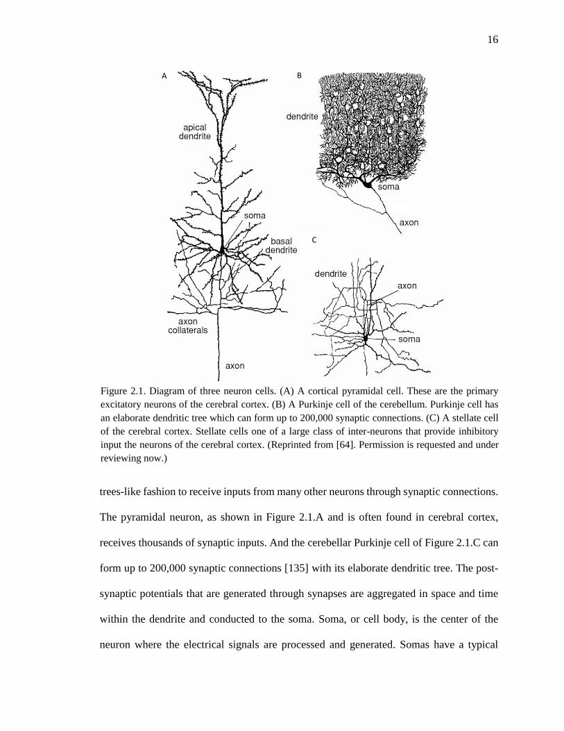
16
trees-like fashion to receive inputs from many other neurons through synaptic connections.
The pyramidal neuron, as shown in Figure 2.1.A and is often found in cerebral cortex,
receives thousands of synaptic inputs. And the cerebellar Purkinje cell of Figure 2.1.C can
form up to 200,000 synaptic connections [135] with its elaborate dendritic tree. The post-
synaptic potentials that are generated through synapses are aggregated in space and time
within the dendrite and conducted to the soma. Soma, or cell body, is the center of the
neuron where the electrical signals are processed and generated. Somas have a typical
A B
C
Figure 2.1. Diagram of three neuron cells. (A) A cortical pyramidal cell. These are the primary
excitatory neurons of the cerebral cortex. (B) A Purkinje cell of the cerebellum. Purkinje cell has
an elaborate dendritic tree which can form up to 200,000 synaptic connections. (C) A stellate cell
of the cerebral cortex. Stellate cells one of a large class of inter-neurons that provide inhibitory
input the neurons of the cerebral cortex. (Reprinted from [64]. Permission is requested and under
reviewing now.)

17
diameter from about 10 µm to 100 µm. The basic method a soma processes the information
is to produce a membrane potential with the aggregated post-synaptic potentials, and
generate an ‘action potential’, or spike for simplicity, once the membrane potential reaches
a threshold, of which the event to emit the action potential is called firing or spiking. After
firing, the neuron becomes insensitive to stimuli during a refractory period of few
milliseconds. Most neurons transmit action potentials down the pre-synaptic terminals,
where the action potential generates post-synaptic potentials through synapses to the
dendrites of other neurons. Axon from single neurons can traverse several millimeters to
reach other regions in the brain. For fast transmission, some axons are covered by myelin
sheaths. And to maintain the signal integrity, they are interrupted by nodes of Ranvier
where, the action potential is regenerated. A few neurons, have no axons or very short
axons transmit graded potentials directly, which decay exponentially.
Neuron Electrical Properties
The electrical properties of the neurons are defined in the relative to their surrounding
extracellular medium, which is conventionally defined to be neutral. Under resting
conditions, a neuron maintain about -70 mV potential inside its cell membrane which is
supported by ion concentration gradients across the membrane. Membrane potential
increases when currents flow into the cell (in the form of positively charged ions flowing
out of the cell), while decreases when currents flow out the cell (in the form of positively
charged ions flowing into the cell). Information processing in a neuron starts from
receiving and summing thousands of post-synaptic current inputs from synapses, and then
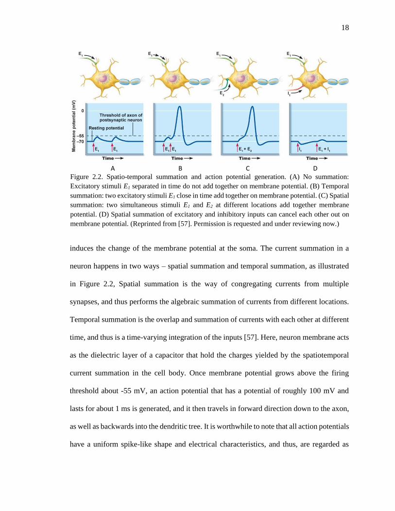
18
induces the change of the membrane potential at the soma. The current summation in a
neuron happens in two ways – spatial summation and temporal summation, as illustrated
in Figure 2.2, Spatial summation is the way of congregating currents from multiple
synapses, and thus performs the algebraic summation of currents from different locations.
Temporal summation is the overlap and summation of currents with each other at different
time, and thus is a time-varying integration of the inputs [57]. Here, neuron membrane acts
as the dielectric layer of a capacitor that hold the charges yielded by the spatiotemporal
current summation in the cell body. Once membrane potential grows above the firing
threshold about -55 mV, an action potential that has a potential of roughly 100 mV and
lasts for about 1 ms is generated, and it then travels in forward direction down to the axon,
as well as backwards into the dendritic tree. It is worthwhile to note that all action potentials
have a uniform spike-like shape and electrical characteristics, and thus, are regarded as
A B C D
Figure 2.2. Spatio-temporal summation and action potential generation. (A) No summation:
Excitatory stimuli E1 separated in time do not add together on membrane potential. (B) Temporal
summation: two excitatory stimuli E1 close in time add together on membrane potential. (C) Spatial
summation: two simultaneous stimuli E1 and E2 at different locations add together membrane
potential. (D) Spatial summation of excitatory and inhibitory inputs can cancel each other out on
membrane potential. (Reprinted from [57]. Permission is requested and under reviewing now.)

19
carrying no sensory information in the shape alone. Instead, their frequency and the exact
timing relative to each other contains information. It also has been found that the shape of
action potential has crucial functionalities as a substrate for modification of synaptic
efficacy.
The primary electrical operation of a neuron could be summarized as integrate and
fire, while considering the dendrite tree as a passive portion. However, neuroscience
experiments also suggest that dendritic tree could act as independent computational units,
e.g. it has been found that synapses can influence each other in the neighboring dendrite
tree, and membrane potentials can be amplified by active spots on dendrite tree [58].
Synapse
Neurons communicate with each other using action potentials, while the medium
that sits between one neuron’s axon and the other neuron, and passed the signal, is termed
as the synapse. Conventionally, the neuron that transmits action potential is called the pre-
synaptic neuron, and the neuron that receives the action potential related signal is called
the post-synaptic neuron. Most of the synapses have their post-synaptic part located at the
spines in the dendritic tree and less frequently at the dendritic shafts. While inhibitory
synapses also contact the soma, where they can have a strong effect on the membrane
potential of the post-synaptic neuron and mute it. Although synapses are highly specialized,
they fall into two categories: chemical synapses which terminate electrical signals and pass
the information from pre-synaptic neuron to post-synaptic neuron using chemical
substances, and electrical synapses that directly pass electrical signals.
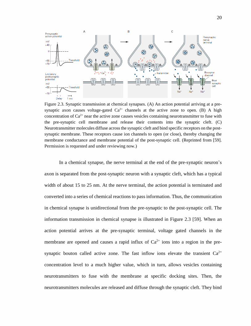
20
In a chemical synapse, the nerve terminal at the end of the pre-synaptic neuron’s
axon is separated from the post-synaptic neuron with a synaptic cleft, which has a typical
width of about 15 to 25 nm. At the nerve terminal, the action potential is terminated and
converted into a series of chemical reactions to pass information. Thus, the communication
in chemical synapse is unidirectional from the pre-synaptic to the post-synaptic cell. The
information transmission in chemical synapse is illustrated in Figure 2.3 [59]. When an
action potential arrives at the pre-synaptic terminal, voltage gated channels in the
membrane are opened and causes a rapid influx of Ca2+ ions into a region in the pre-
synaptic bouton called active zone. The fast inflow ions elevate the transient Ca2+
concentration level to a much higher value, which in turn, allows vesicles containing
neurotransmitters to fuse with the membrane at specific docking sites. Then, the
neurotransmitters molecules are released and diffuse through the synaptic cleft. They bind
Figure 2.3. Synaptic transmission at chemical synapses. (A) An action potential arriving at a pre-
synaptic axon causes voltage-gated Ca2+ channels at the active zone to open. (B) A high
concentration of Ca2+ near the active zone causes vesicles containing neurotransmitter to fuse with
the pre-synaptic cell membrane and release their contents into the synaptic cleft. (C)
Neurotransmitter molecules diffuse across the synaptic cleft and bind specific receptors on the post-
synaptic membrane. These receptors cause ion channels to open (or close), thereby changing the
membrane conductance and membrane potential of the post-synaptic cell. (Reprinted from [59].
Permission is requested and under reviewing now.)
21
to the corresponding receptors on the post-synaptic membrane, that open or close ion
channels in its vicinity. As a result, ions flow into post-synaptic neuron and build a post-
synaptic potential (PSP). The post-synaptic potential can be either excitatory (EPSP) or
inhibitory (IPSP), depending on the type of the pre-synaptic neuron. Typically, a EPSP
increases the membrane potential from its resting potential and brings it closer towards the
firing threshold; while a IPSP decreases the membrane potential from its resting potential.
Electrical synapses connect the membranes of two neurons directly with a gap-
junction. The ion channels on the two sides of gap are aligned, and thus, allow ions to pass
through channels quickly in both the directions. Consequently, electrical signal runs
through an electrical synapse even if it is below the threshold for an action potential.
Because the communication is fast, neurons use electrical synapses to synchronize their
activity.
The strength (or efficacy) of both of electrical and chemical synaptic transmission
can be enhanced or diminished, called synaptic plasticity, according to pre- and post-
synaptic activities. The enhancement of synaptic strength is also called potentiation and
equivalents to an increase in synaptic conductance, while the diminution is called
depression and equivalents to a reduction in synaptic conductance. The time-scale of
synaptic potentiation and depression varies from milliseconds to several minutes (short-
term), or from several hours to days (long-term). Here the long term potentiation (LTP) is
widely considered to be responsible for the underlying learning and memory in the brain.
There are many cellular mechanisms involved in the formation of LTP, where neuroscience
experiments have shown that permanent structure changes could lead to LTP. These

22
structure changes include emergence of additional post-synaptic receptors, enlargement of
axon terminal, and growth of new spines.
Neuron Models
McCulloch-Pitts Model
Even though a majority part of the human brain still remains less understood even
after a century’s research, the development of capturing its structure, behavior and
mathematical modelling for application can be traced back to 1943. In that year, McCulloch
and Pitts proposed a neuro-inspired computing model [5], which described a neuron into a
mathematical weight summing and linear thresholding gate. In mathematical form, it
describes a neuron with a set of inputs x1, x2, x3, …, xn and one output y. The linear threshold
gate simply classifies the set of inputs into two different classes, “0” or “1”, and can be
generalized in mathmatical equations
𝑠 = ∑ 𝑤𝑖𝑥𝑖
𝑛
𝑖=1
𝑦 = 𝜑(𝑠, 𝜃)
where wi are the weight values representing the synpatic connection strength, s is the the
weighted sum and equavilent to the neuron membrane voltage. The φ is called activation
function which depends on the weighted sum s and the firing threshold θ, and was selected
as a Heaviside step function at the beginning. The McCulloch-Pitts model of a neuron is
simple yet has captured the fundamental features and operating behavior of biological
neurons.

23
The McCulloch-Pitts model highly abstracts the fundamental neuron behavior
without taking many neural network properties into consideration. Moreover, the
mathematical formulation of the back-propagation algorithm needs intensive computing
power and is far away from the actual biological spike-based neural networks. Thus, this
model is not hardware-friendly and difficult to be used in neuroscience research. By
looking more closely at the biological neurons and biological neural networks,
neuroscientists and engineers have formulated more accurate representations of neuron,
synapse and network architecture that can provide much more computational power.
A biological neuron has its outputs in the form of short electrical pulses, termed as
action potentials or spikes. The shape of the pulse does not change as the action potential
propagates along the axon, and all spikes from the same neuron look alike. As a result, the
shape of the spike does not carry any information and is noted as 0 or 1in the classic ANNs.
However, the number and the timing of the spikes can matter and, in fact, are
computationally useful, which is the fundamental property neglected by the simple
McCulloch-Pitts model.
Leaky Integrate-and-Fire Model
The neuron behavior can be also modeled in terms of the spike generation
mechanism. The leaky integrate-and-fire (LIF) neuron is probably the best-known example
of such an abstracted spiking neuron model. The LIF neuron model captures the most basic
property of biological neurons; it integrates injected currents over time and generates an
action potential whenever its membrane potential Vmem crosses a firing threshold value Vthr.
After the firing, the membrane potential goes back to a rest value Vrest below the threshold
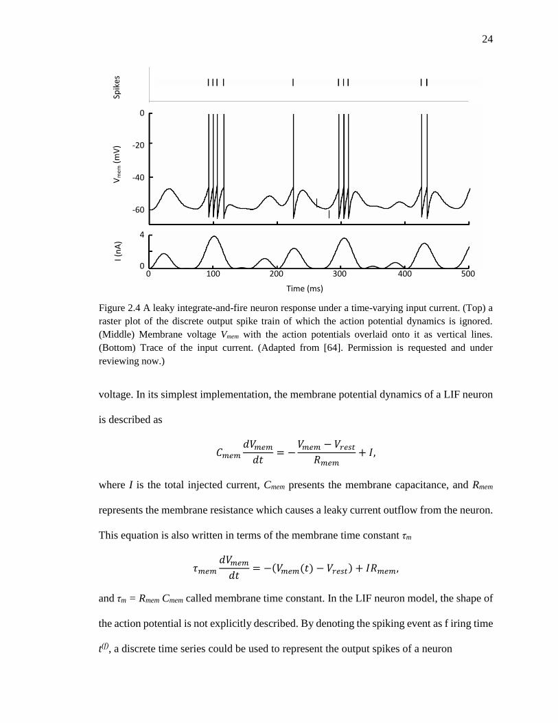
24
voltage. In its simplest implementation, the membrane potential dynamics of a LIF neuron
is described as
𝐶𝑚𝑒𝑚
𝑑𝑉𝑚𝑒𝑚
𝑑𝑡= −
𝑉𝑚𝑒𝑚 − 𝑉𝑟𝑒𝑠𝑡
𝑅𝑚𝑒𝑚+ 𝐼,
where I is the total injected current, Cmem presents the membrane capacitance, and Rmem
represents the membrane resistance which causes a leaky current outflow from the neuron.
This equation is also written in terms of the membrane time constant τm
𝜏𝑚𝑒𝑚
𝑑𝑉𝑚𝑒𝑚
𝑑𝑡= −(𝑉𝑚𝑒𝑚(𝑡) − 𝑉𝑟𝑒𝑠𝑡) + 𝐼𝑅𝑚𝑒𝑚,
and τm = Rmem Cmem called membrane time constant. In the LIF neuron model, the shape of
the action potential is not explicitly described. By denoting the spiking event as f iring time
t(f), a discrete time series could be used to represent the output spikes of a neuron
Time (ms)
Vm
em (
mV
)I (
nA
)Sp
ikes
0
4
-60
-40
-20
0
0 100 200 300 400 500
Figure 2.4 A leaky integrate-and-fire neuron response under a time-varying input current. (Top) a
raster plot of the discrete output spike train of which the action potential dynamics is ignored.
(Middle) Membrane voltage Vmem with the action potentials overlaid onto it as vertical lines.
(Bottom) Trace of the input current. (Adapted from [64]. Permission is requested and under
reviewing now.)
25
𝑡(𝑓): 𝑉𝑚𝑒𝑚(𝑡(𝑓)) = 𝑉𝑡ℎ𝑟 .
The LIF neuron model is a single compartment model i.e. it has only one variable
Vmem that models the subthreshold membrane potential dynamics. It doesn’t specify the
action potential shape, and membrane capacitance and resistance are time independent
which is not the case in biological neurons. However, if the action potential dynamics is a
not a primary factor in computation, and the variations in membrane parameters can be
ignored, the LIF model provides a very efficient and effective representation of spiking
neuron behavior.
Hodgkin and Huxley Model
From a biophysical point of view, spike potentials are the result of currents that
pass through ion channels in the cell membrane. In an extensive series of experiments on
the giant axon of the squid, Hodgkin and Huxley succeeded in measuring these currents
and describing their dynamics in terms of four nonlinear ordinary differential equations
[60]. Hodgkin and Huxley model precisely captured the conductance changes in sodium,
potassium and leak channels as functions of channel potentials, and models the neuron
membrane potential as a function of the channel currents. While the Hodgkin-Huxley
model is regarded as one of the great achievements of 20th century biophysics, its
computational complexity severely limits its applicability to large scale models and
engineering applications. Furthermore, it is unclear from a computational perspective
whether the exact details of the ion channels are necessary, or if they are simply artifacts
of biology’s implementation. Modeling at the level of the Hodgkin-Huxley neuron may be
key to building a one-to-one correspondence model of the brain, but the computational
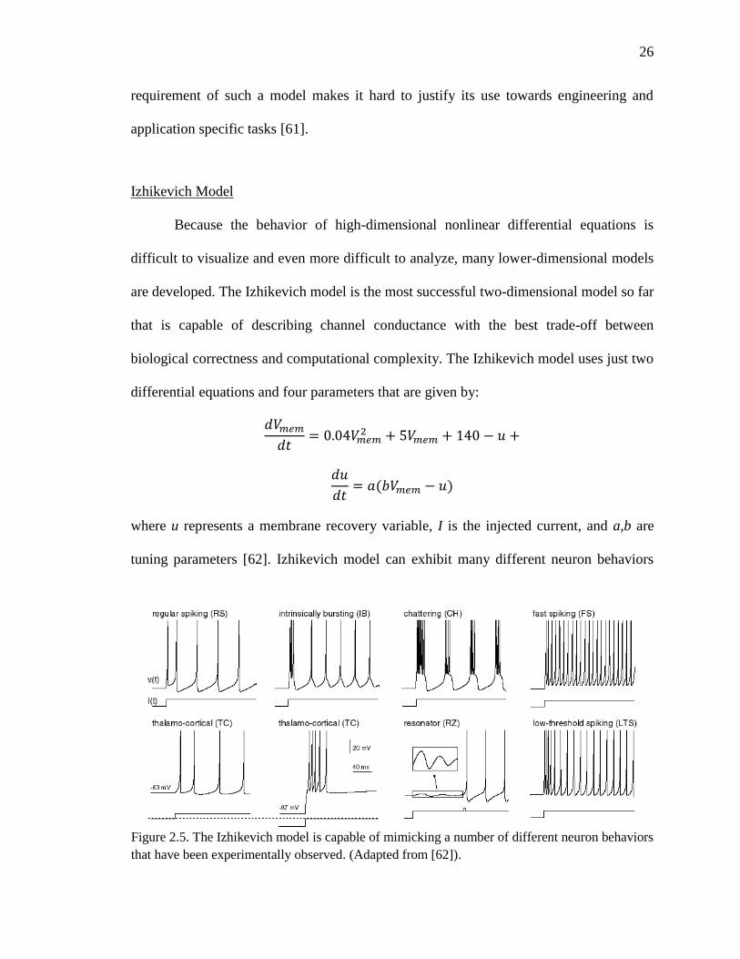
26
requirement of such a model makes it hard to justify its use towards engineering and
application specific tasks [61].
Izhikevich Model
Because the behavior of high-dimensional nonlinear differential equations is
difficult to visualize and even more difficult to analyze, many lower-dimensional models
are developed. The Izhikevich model is the most successful two-dimensional model so far
that is capable of describing channel conductance with the best trade-off between
biological correctness and computational complexity. The Izhikevich model uses just two
differential equations and four parameters that are given by:
𝑑𝑉𝑚𝑒𝑚
𝑑𝑡= 0.04𝑉𝑚𝑒𝑚
2 + 5𝑉𝑚𝑒𝑚 + 140 − 𝑢 +
𝑑𝑢
𝑑𝑡= 𝑎(𝑏𝑉𝑚𝑒𝑚 − 𝑢)
where u represents a membrane recovery variable, I is the injected current, and a,b are
tuning parameters [62]. Izhikevich model can exhibit many different neuron behaviors
Figure 2.5. The Izhikevich model is capable of mimicking a number of different neuron behaviors
that have been experimentally observed. (Adapted from [62]).

27
observed in biological experiments such as tonic spiking, bursting, and spike-frequency
adaptation, as shown in Figure 2.5. However, from the current understanding from
computational neuroscience, faithful mathematical fitting a model to the neuron behavior
tells neither the procedure of information processing occurring in a neuron nor their role in
computation. Therefore, such models are difficult to be used for study of neural encoding,
memory, network dynamics, and guiding the construction of artificial neural hardware.
Brain-Inspired Learning
Spike-timing dependent plasticity (STDP) of synapses and its modifications are
widely believed to be the underlying learning mechanism in the brain. Many neuroscience
experiments have revealed that spike-dependent processes can produce short-term changes
in the efficacies of synapses, as well as form permanent connections among neurons. The
changes in synaptic efficacy make a neuron to respond to certain stimulations only, and
then eventually become selective. Furthermore, experimental and theoretical studies also
suggest a group of neurons organized in a recurrent manner can compete and form different
selective pattern to the shared inputs. Inspired by these mechanisms, a wide variety of
computing tasks including associative learning, auto-encoding, pattern recognition, time-
series predication, function approximation and memory storage and recall can be realized.
Hebbian Learning
In 1949, Donald Hebb describes a basic mechanism for synaptic plasticity, where
an increase in synaptic strength arises from the pre-synaptic cell's repeated and persistent
stimulation of the post-synaptic cell [63]. This Hebbian learning theory is often
summarized to "neurons that fire together, wire together". From the point of view of
28
artificial neural networks, Hebb's principle can be described as a method of altering the
synaptic weights w between neuron units depending on their relative activities. This
insightful observation partially inspired the development of artificial neural networks.
The basic Hebb’s rule can be put in a mathematical form with the integrate and fire
model
𝜂𝑑𝒘
𝑑𝑡= (𝒘𝒙𝑻)𝒙 = 𝑦𝒙,
where x is a matrix of the pre-synaptic spiking inputs, y is the neuron output equals to the
dot product of x and w, and η is the learning rate. Using 0 and 1 to represent no spike and
the presence of a spike, this equation tells that weights increase with the existence of
respective correlated pre- and post-synaptic spikes during a given small time interval.
When interpreting this in a statistical manner, x is spike trains of the pre-synaptic neurons
following certain distribution (e.g. Poisson), y is the spike train of the post-synaptic neuron,
and thus the basic Hebb’s rule describes the probability of the changes to the synapses
depending on the neurons coincident activities.
Theoretical analysis shows the basic Hebb’s rule, in fact, approaches to the
principle component analysis (PCA) [64], [65]. As result, it yields the weight vector an
approximation to the first principle component of the given input stimulation. However,
Hebbian learning is not stable, because the weight values grow with time until they are all
saturated. As result, the neuron loses its selectivity. There are several mathematical ways
to modify and stabilize Hebb’s rule, e.g. subtractive normalization and Oja’s rule [64], but
they are not biology plausible and difficult to embedded with a neural network in a natural
way.

29
Spike Timing Dependent Plasticity
The original Hebb’s rule reflects the one side of the synaptic plasticity, that is
potentiation or weight increase. The other side, synapses depress or decrease weight when
the pre- and post-synaptic neurons fire together, was studied and formulated with
experimental evidence, and named anti-Hebb’s rule. Hebb’s rule relates the synaptic
changes with the timing of activities of pre- and post-synaptic neurons in a very rough way
– “together”; while the precise relations with time was not seriously studied until the
1990’s.
In 1993, the precise spike-timing information between pre- and post-synaptic
neurons was used to modulate synapse strength in a neural network simulation without
considering it as biologically plausible [66]. Five years later, in vivo experiments of cortical
pyramidal cells showed that the relative timing of the pre- and post-synaptic spike pairs is
critical in determining the amount and type of synaptic modification that takes place [67].
In the following years, this discovery was double confirmed and summarized as the spike-
timing dependent plasticity (STDP) in a well-known formula today [22]–[24], [67]–[69].
STDP states that the synaptic weight w is modulated according to the relative timing of the
pre- and post-synaptic neuron firing. As illustrated in Figure 2.6, a spike pair with the pre-
synaptic spike arrives before the post-synaptic spike results in increasing the synaptic
strength (or potentiation); a pre-synaptic spike after a post-synaptic spike results in
decreasing the synaptic strength (or depression). Changes of the synaptic weight plotted as
a function of the relative arrival timing Δt of the post-synaptic spike with respect to the pre-
synaptic spike is called the STDP function or learning window. A popular choice for the
STDP function Δw is
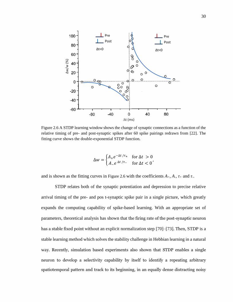
30
∆𝑤 = 𝐴+𝑒−∆𝑡 /𝜏+ for ∆𝑡 > 0
𝐴−𝑒 ∆𝑡 /𝜏− for ∆𝑡 < 0,
and is shown as the fitting curves in Figure 2.6 with the coefficients A+, A-, τ+ and τ-.
STDP relates both of the synaptic potentiation and depression to precise relative
arrival timing of the pre- and pos t-synaptic spike pair in a single picture, which greatly
expands the computing capability of spike-based learning. With an appropriate set of
parameters, theoretical analysis has shown that the firing rate of the post-synaptic neuron
has a stable fixed point without an explicit normalization step [70]–[73]. Then, STDP is a
stable learning method which solves the stability challenge in Hebbian learning in a natural
way. Recently, simulation based experiments also shown that STDP enables a single
neuron to develop a selectivity capability by itself to identify a repeating arbitrary
spatiotemporal pattern and track to its beginning, in an equally dense distracting noisy
w
/w (
%)
t (ms)
Pre
Post
Δt<0
Pre
Post
Δt<0
Figure 2.6 A STDP learning window shows the change of synaptic connections as a function of the
relative timing of pre- and post-synaptic spikes after 60 spike pairings redrawn from [22]. The
fitting curve shows the double-exponential STDP function.

31
background [74]. Besides above basic pair-wise learning rule, STDP has many varieties
[73], [75]. Future experiments have shown the relative voltage of the pre- and post-synaptic
spike pair is the more fundamental than spike timing [24], [73], which will become explicit
and critical in modeling and realizing the in situ modulation of nanoscale RRAM devices
later. Last and important, because STDP is a local learning rule – which implies that the
change of synapse weight depends only on the activities of the two neurons connected by
the it, and therefore, there is not von Neumann bottleneck at all, at the same time, the
circuits driving the learning could be very simple.
Associative Learning
Associative learning is a simple analogous to the classical conditioning which is
the foundation of animal behavior and refers to a learning procedure in which an unrelated
stimulus is paired with a reinforcing stimulus, such as rewards or punishment, by virtue of
the repeated correlation. Associative learning was first studied in detail by Pavlov’s studies
with salivation response in dogs in 1927. In his seminal experimental test, Pavlov fed the
dog food which is an unconditioned stimulus that is independent of previous experience,
and at the same time, presented a bell sound which is a conditional stimulus depending on
its association with food. After a few repeats, the dogs started to salivate in response to
only to the bell sound.
The neural substrate of simplified associative learning could be modeled by a neural
network with two input neurons for sensory and one output neurons for association
decision. In this small network, one of the two sensory neurons presents the unconditioned
stimulus, and cause the output neuron fires. If, at the same, another stimulus was given to
the other sensory neuron, by applying Hebbian learning rule, the connection between this

32
sensory neuron and the output neuron will get strengthened. After sufficient repeats in the
same way, the strengthened connection finally causes firing of output neuron
independently.
Associative learning is a dynamic process with the synaptic connections developing
according to the relationships between a new stimulus with the existing one, and thus, could
be considered as a minimum form of supervised learning. It is worth to point out that
associative learning in the real brain is a complicated process instead of a single neuron
reaction. There is substantial evidence that many chemical substances, like dopamine, are
involved in the reward learning at the system level. Despite it doesn’t account to explain
the classical conditioning in animal brains, the single neuron model inspires a useful way
to implement reinforced learning in hardware.
Competitive Learning
STDP enables in situ synaptic potentiation and depression depending on the local
neurons that are locally connected to a synapse, and then enables a neuron to become
selective to successive coincidences of a pattern. When a group of neurons are working
together, the depression between each other or among a group of neurons with recurrent
connections could make these multi-neuron systems achieve high-level functionality. In a
brain, the mutual depression is generally achieved through lateral inhibition, which is a
decrease in the activity of one neuron resulting from the stimulation of its neighbors.
Lateral inhibition is an extremely common characteristics of the brain’s sensory
path. The on-center and off-center cells of the auditory system, the somatosensory system,
and the visual system in brains are the consequence of lateral inhibition. For example, a
retina on-center cell increases its firing rate when the center of its receptive field is exposed
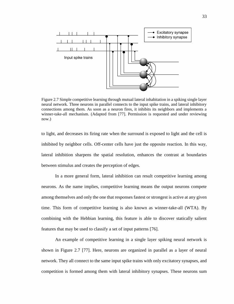
33
to light, and decreases its firing rate when the surround is exposed to light and the cell is
inhibited by neighbor cells. Off-center cells have just the opposite reaction. In this way,
lateral inhibition sharpens the spatial resolution, enhances the contrast at boundaries
between stimulus and creates the perception of edges.
In a more general form, lateral inhibition can result competitive learning among
neurons. As the name implies, competitive learning means the output neurons compete
among themselves and only the one that responses fastest or strongest is active at any given
time. This form of competitive learning is also known as winner-take-all (WTA). By
combining with the Hebbian learning, this feature is able to discover statically salient
features that may be used to classify a set of input patterns [76].
An example of competitive learning in a single layer spiking neural network is
shown in Figure 2.7 [77]. Here, neurons are organized in parallel as a layer of neural
network. They all connect to the same input spike trains with only excitatory synapses, and
competition is formed among them with lateral inhibitory synapses. These neurons sum
Figure 2.7 Simple competitive learning through mutual lateral inhabitation in a spiking single layer
neural network. Three neurons in parallel connects to the input spike trains, and lateral inhibitory
connections among them. As soon as a neuron fires, it inhibits its neighbors and implements a
winner-take-all mechanism. (Adapted from [77]. Permission is requested and under reviewing
now.)

34
the inputs current and generate their membrane potentials, of which the fastest growing
one is the neuron has its synaptic weight best matching to the inputs. As soon as the neuron
fires, it sends a signal to inhibit all of its neighbors, and the only its synapses will be
changed under learning rule – meaning the winner takes all. We have mentioned that
Hebbian learning realized an approximation to find the first PCA component of the inputs,
the WTA mechanism enables the neurons to trace different patterns in the inputs in each
spiking event, and find their first PCA component respectively. Together, this group of
neurons identifies characteristic patterns and saves them as fixed filter-like templates in
their synaptic connections. Later, the pattern classification task is performed by matching
the fixed filter-like templates to the new input activity profile through competition again.
Using the binary output spike train notation yi the i-th neuron, WTA can be expressed as
𝑦𝑖 = 1, if 𝑣𝑖 > 𝑣𝑗 for all 𝑗, 𝑗 ≠ 𝑖
0, otherwise ,
where vi represents the membrane potential just before the firing of the i-th neuron, and the
respective synaptic weight is updated according to the learning rule.
WTA can be mathematically interpreted as the maximum likelihood decoding
method [64], and more theoretical work has proved that the combination of WTA and
STDP realizes optimal parameter identification in terms of Bayesian expectation-
maximization algorithm [31], and hidden Markov model learning [78].

35
Brain-Inspired Architectures
Perceptron
In the following one decade of the invention of McCulloch-Pitts neural model, by
the combining Hebbian learning, Frank Rosenblatt introduced the first generation of
artificial neural network, the perceptron, in 1958. Perceptron is a binary classifier which a
neural network composed of several associative neuron units as inputs, a decision neuron
unit as outputs, and an algorithm for supervised learning [6]. Specially, bias of a neuron is
used in perceptron algorithm, which can be considered as an additional constant 1 input (x0
= 1) to a weight with the value equals the bias (w0 = b) in the previous generalized neuron
model. A subsequently implemented hardware with an array of photocells as neurons and
potentiometers as synapses may be the first neuro-inspired computing hardware. However,
it was quickly proved that such a perceptron could only be used to discriminate linearly
separable data, while the non-linearly separable problems like XOR function were
impossible for it to classify [79]. This led to the field of neural network research stagnating
for several years.
Multi-Level Perceptron
In 1970’s, it was recognized that a multilayer perceptron (MLP) had far greater
processing power [80], where there is at least one hidden layer between inputs and outputs
as shown in Figure 2.8. In 1986, Rumelhart, Hinton and Williams applied backpropagation
(BP) algorithm to the MLP network [81]. Moreover, researchers noted that biological
neurons are sending the signal in patterns of spikes rather than simple absence or presence
of single spike pulse, and a number of continuous activation functions φ, such the sigmoid,
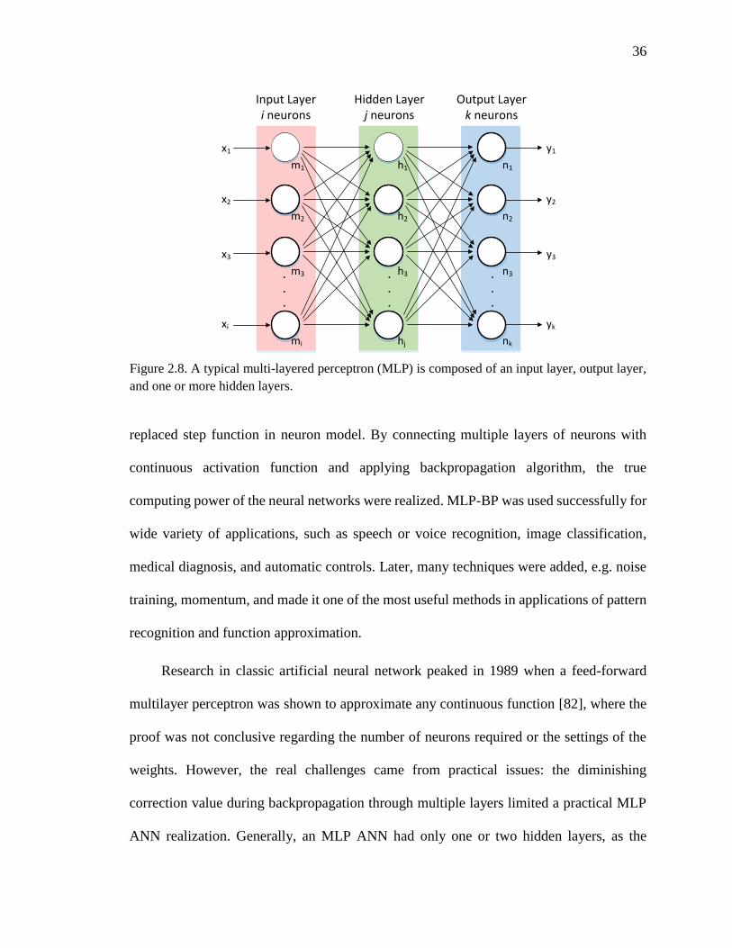
36
replaced step function in neuron model. By connecting multiple layers of neurons with
continuous activation function and applying backpropagation algorithm, the true
computing power of the neural networks were realized. MLP-BP was used successfully for
wide variety of applications, such as speech or voice recognition, image classification,
medical diagnosis, and automatic controls. Later, many techniques were added, e.g. noise
training, momentum, and made it one of the most useful methods in applications of pattern
recognition and function approximation.
Research in classic artificial neural network peaked in 1989 when a feed-forward
multilayer perceptron was shown to approximate any continuous function [82], where the
proof was not conclusive regarding the number of neurons required or the settings of the
weights. However, the real challenges came from practical issues: the diminishing
correction value during backpropagation through multiple layers limited a practical MLP
ANN realization. Generally, an MLP ANN had only one or two hidden layers, as the
.
.
.
.
.
.
.
.
.
y1
y2
y3
yk
n1
n2
n3
nk
h1
h2
h3
hj
m1
m2
m3
mi
x1
x2
x3
xi
Input Layeri neurons
Hidden Layerj neurons
Output Layerk neurons
Figure 2.8. A typical multi-layered perceptron (MLP) is composed of an input layer, output layer,
and one or more hidden layers.
37
limited computing capability at that time restricted the ANN training to only small scale
neural networks. These issues remained a roadblock in the next ten years, until another
wave of brain inspiration arrived in the field of artificial neural networks. Interestingly, in
the same year, an MLP with a modified architecture was used for handwritten digits
recognition and started to brew the latest deep learning storm [83], and the concept of brain-
inspired neuromorphic hardware was proposed [84].
Recurrent Networks
Perceptrons are feedforward neural networks wherein their connections between the
neurons go in only one direction and do not form a cycle. While in general, the connections
in a neural network can form a directed cycle, called recurrent neural networks (RNN). The
competitive learning network with lateral inhibitions is an example of the recurrent neural
network. The cycled connections in RNN create internal states which allow the network to
exhibit dynamic temporal behavior. As a result, RNNs can use their internal memory to
process arbitrary sequences of inputs, e.g. speech waveforms and financial time-series data.
Besides competitive learning network, there are several types of RNNs. The Hopfield
network is a symmetrically connected RNN which serves as content-addressable memory
system with interconnection alteration under Hebbian learning rule. A liquid state machine
(LSM) consists of a large collection of randomly connected non-linear neurons with linear
read-out units. The recurrent nature of the connections turns the input into a spatio-
temporal pattern of activations in the network nodes and realizes a large variety of
nonlinear functions. The LSM can theoretically perform any mathematical operation by
linearly combining the network states and forms a universal function approximation.
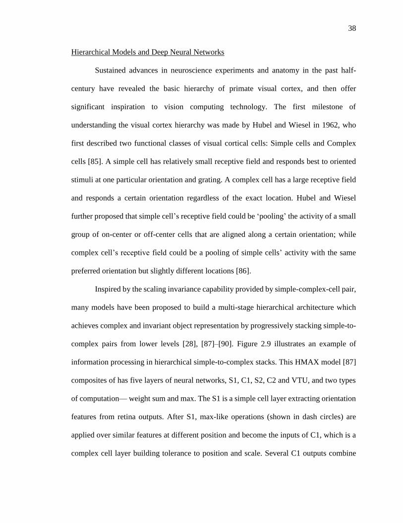
38
Hierarchical Models and Deep Neural Networks
Sustained advances in neuroscience experiments and anatomy in the past half-
century have revealed the basic hierarchy of primate visual cortex, and then offer
significant inspiration to vision computing technology. The first milestone of
understanding the visual cortex hierarchy was made by Hubel and Wiesel in 1962, who
first described two functional classes of visual cortical cells: Simple cells and Complex
cells [85]. A simple cell has relatively small receptive field and responds best to oriented
stimuli at one particular orientation and grating. A complex cell has a large receptive field
and responds a certain orientation regardless of the exact location. Hubel and Wiesel
further proposed that simple cell’s receptive field could be ‘pooling’ the activity of a small
group of on-center or off-center cells that are aligned along a certain orientation; while
complex cell’s receptive field could be a pooling of simple cells’ activity with the same
preferred orientation but slightly different locations [86].
Inspired by the scaling invariance capability provided by simple-complex-cell pair,
many models have been proposed to build a multi-stage hierarchical architecture which
achieves complex and invariant object representation by progressively stacking simple-to-
complex pairs from lower levels [28], [87]–[90]. Figure 2.9 illustrates an example of
information processing in hierarchical simple-to-complex stacks. This HMAX model [87]
composites of has five layers of neural networks, S1, C1, S2, C2 and VTU, and two types
of computation— weight sum and max. The S1 is a simple cell layer extracting orientation
features from retina outputs. After S1, max-like operations (shown in dash circles) are
applied over similar features at different position and become the inputs of C1, which is a
complex cell layer building tolerance to position and scale. Several C1 outputs combine
39
under a bell-shaped tuning operation (shown in plain circle) and form complicated features
extracted in S2, a higher level simple cell layer, to increase complexity of the underlying
representation. Furthermore, C2, the high er level complex cell, further combines feature
from C1 and S2 and forms complicated features. The fifth layer is a full connection between
C2 and VTU, which contains view-tuned cells that are tolerant to scaling and translation
of their preferred object view. Recent research has shown that the simple-cell-like receptive
field could emerge from unsupervised learning to natural scene images [91]. Also
Figure 2.9 The basic HMAX model consists of a hierarchy of five levels, from the S1 layer with
simple-cell like response properties to the level with shape tuning and invariance properties like
the view-tuned cells. (Reprinted with permission from [87] © 1999 Macmillan Publishers Ltd:
Nature Neuroscience).

40
biologically plausible unsupervised receptive field formation has been shown using STDP
local learning rule [92].
Hierarchical organization provides a solution to the invariance object recognition
by decomposing a complex task in a hierarchy of simpler ones that can be easily processed
at each stage. In addition, employing the hierarchical stacking of simple building blocks
enables a better use of computational resources to achieve high energy efficiency. For
instance, the lowest levels of the hierarchy may represent a dictionary of features that can
be shared across multiple classification tasks [93].
Hierarchical visual cortex inspired the development of immensely popular
convolutional neural networks (CNNs) as well, which is the starting point of deep neural
networks (DNNs). In 1980, Kunihiko Fukushima introduced Neocognitron [94] which is a
multi-layer neural network with its first layer operating in convolutional manner to extract
local features and then cascades it in the simple-to-complex manner. Later, LeCun
designed his deep neural networks [83], [95] with a customized connecting schema that
can be trained with standard backpropagation algorithm to recognize handwritten postal
codes on mails, as shown in Figure 2.10.
However, similar to the MLP, CNN experienced the issue of vanishing gradient
[96] and is difficult to train in general manner, until several techniques were invented later.
One of the critical techniques is layer-wise pre-training used in Schmidhuber's multi-level
hierarchy of networks, in which each layer is pre-trained one at a time through
unsupervised learning, and then fine-tuned through backpropagation [97]. Other
techniques include choosing appropriate activation functions, e.g. using rectified linear
units (ReLU) to replace conventional sigmoid function [98], and loss functions, e.g. using
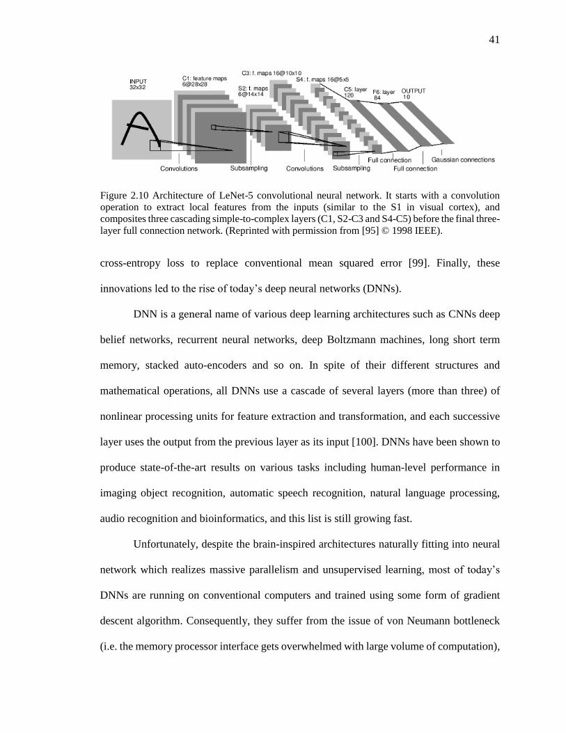
41
cross-entropy loss to replace conventional mean squared error [99]. Finally, these
innovations led to the rise of today’s deep neural networks (DNNs).
DNN is a general name of various deep learning architectures such as CNNs deep
belief networks, recurrent neural networks, deep Boltzmann machines, long short term
memory, stacked auto-encoders and so on. In spite of their different structures and
mathematical operations, all DNNs use a cascade of several layers (more than three) of
nonlinear processing units for feature extraction and transformation, and each successive
layer uses the output from the previous layer as its input [100]. DNNs have been shown to
produce state-of-the-art results on various tasks including human-level performance in
imaging object recognition, automatic speech recognition, natural language processing,
audio recognition and bioinformatics, and this list is still growing fast.
Unfortunately, despite the brain-inspired architectures naturally fitting into neural
network which realizes massive parallelism and unsupervised learning, most of today’s
DNNs are running on conventional computers and trained using some form of gradient
descent algorithm. Consequently, they suffer from the issue of von Neumann bottleneck
(i.e. the memory processor interface gets overwhelmed with large volume of computation),
Figure 2.10 Architecture of LeNet-5 convolutional neural network. It starts with a convolution
operation to extract local features from the inputs (similar to the S1 in visual cortex), and
composites three cascading simple-to-complex layers (C1, S2-C3 and S4-C5) before the final three-
layer full connection network. (Reprinted with permission from [95] © 1998 IEEE).
42
with unsustainable energy consumption. Thus, the brain-inspiration should not only be
adopted at the software and algorithm level, but should also be wholeheartedly explored at
the computing hardware architecture level. Such synergistic exploration will realize the
ANN algorithms on a suitable hardware substrate, and truly unleash the computing power
of the brain-inspired architectures.
Summary
Neurons and synapses are understood to be the fundamental and core elements that
are responsible for learning and computing occurring in the brain. Morphologies and
electrical properties of the neuron and synapse are reviewed in the beginning of this
chapter. Neuron lies at the center of neural information processing. Major neuron models
that capture neuron operation with different level of details are introduced. Based on the
fidelity to represent neuron dynamics and complexity, LIF model abstracts the primary
operation of a neuron in a compact form, and thus, is suitable for computing hardware,
while Hodgkin-Huxley model and its simplified forms fit into bio-realistic neural system
emulation. Synapses are understood to be the locations where learning takes place in the
brain. It is shown that a single neuron can work as a maximum likelihood detector and
finds the first PCA component of the inputs by modulating its synapses under Hebbian
learning rule. Further, the more fundamental mechanism of changing synaptic strength is
discussed in STDP learning rule. The discovery of STDP is a significant contribution to
neuroscience. It descripts the synaptic change as a function of precise relative timing of
pre- and post-synaptic spikes, and enables a form of in situ learning depending on relative
potentials, and paves a solid path for brain- and nanotechnology inspired computing
system. Next, a brief introduction of the associative learning as a simple model of classic
43
conditioning was given. With multiple neurons, the competitive learning and WTA were
discussed. They work with Hebbian and STDP learning together provides a simple but
effective way for a small group of neurons to selectively discriminate patterns from
spatiotemporal inputs, and forms the basic neural circuitry to build complex network for
handling complicated tasks. At the neural network level, a brief history of the artificial
neural network, from the perceptron to latest deep neural networks, was reviewed. It has
been shown that, by progressively stacking simple neural structure from lower levels, a
multi-stage hierarchical architecture can perform complicated computing tasks, like
invariant object representation, with significant efficiency in term of both space occupation
and energy consumption. As a conclusion, the emerging understanding brain from the
experimental and computational neuroscience communities inspires a potential new
computing paradigm in many aspects: from the basic hardware elements, to learning
methods, and finally system architectures. These inspirations need to be assembled
cohesively to form an effective synergy, so that they can successfully address the grand
computing challenges of the present age.
44
CHAPTER 3
NANOTECHNOLOGY FOR NEUROMORPHIC COMPUTING
The history of computing technology development is accompanied with the
sustained advancement in memory technologies. In the continuing era of von Neumann
computers, both the temporary and permanent data storage has been fulfilled by the
CMOS-based memories, e.g. PROM, SRAM, DRAM, and Flash memory ICs. Despite the
semiconductor device technology specifically for memory has been evolving even faster
than the digital CMOS for computing logic, the speed gap between memory and logic is
unavoidable in von Neumann architecture. Moreover, as CMOS technology is approaching
its scaling limits, the power consumption of computer memories has been accounting for a
significant percent of the overall energy budget. In this context, many nanoscale non-
volatile memories (NVMs) have been proposed and have demonstrated significant progress
in recent years. These new NVMs address the two major challenges of energy efficiency
and nanoscale scaling with novel structures. To alleviate this, new materials and innovative
integration schemes have demonstrated great potential to achieve ultra-high energy-
efficiency, high-density, and good scalability. These new memory devices also bring new
functionalities, where biologically plausible synaptic plasticity have been experimentally
demonstrated in various nanoscale memory devices. This convergence of energy-
efficiency, high-density, and biologically plausible synaptic plasticity on the nanoscale

45
memory devices inspires a new computing paradigm beyond the conventional von
Neumann architecture. By synergistic integration of these nanoscale devices as electrical
synapses in the brain-inspired computing architecture, it is very promising to realize
neuromorphic computing systems with computing capability and energy-efficiency
approaching towards biological brains. This chapter reviews the emerging non-volatile
memory technologies, focuses on the resistive random access memory (RRAM) and
discusses its operations and integration in relevance to brain-inspired computing.
Overview of Emerging Memory Technologies
Mainstream memory devices today storage information by means of charging
capacitive cells in CMOS circuits, e.g. SRAM stores charge on parasitic capacitors, with
positive feedback, in cross-coupled inverters; DRAM stores charges on a capacitor cell,
and Flash memory stores charge on a floating gate structure or through other charge
trapping mechanisms. As CMOS technology scaled down to nanometer dimension, the
charge on the tiny capacitor becomes susceptible to leak away which results in reduced
retention and degraded reliability. Consequently, frequent refresh is required to retain the
information and results in increased power consumption.
In this context, the emerging memories are mainly non-charge-based non-volatile
memories which retain information in change in material and/or structural properties. To
achieve this target, emerging NVMs generally employ materials different from those of
mature memories based on CMOS, and yield radically different information retention
mechanisms. These materials include ferroelectric dielectrics, ferromagnetic metals,
chalcogenides, transitional metal oxides, carbon-based materials, etc. Further, their
switching mechanisms extend beyond classical electronic processes, to quantum
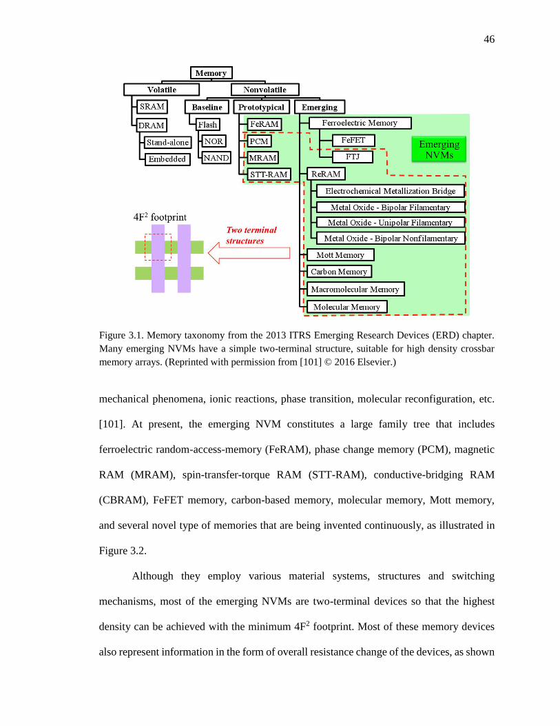
46
mechanical phenomena, ionic reactions, phase transition, molecular reconfiguration, etc.
[101]. At present, the emerging NVM constitutes a large family tree that includes
ferroelectric random-access-memory (FeRAM), phase change memory (PCM), magnetic
RAM (MRAM), spin-transfer-torque RAM (STT-RAM), conductive-bridging RAM
(CBRAM), FeFET memory, carbon-based memory, molecular memory, Mott memory,
and several novel type of memories that are being invented continuously, as illustrated in
Figure 3.2.
Although they employ various material systems, structures and switching
mechanisms, most of the emerging NVMs are two-terminal devices so that the highest
density can be achieved with the minimum 4F2 footprint. Most of these memory devices
also represent information in the form of overall resistance change of the devices, as shown
Figure 3.1. Memory taxonomy from the 2013 ITRS Emerging Research Devices (ERD) chapter.
Many emerging NVMs have a simple two-terminal structure, suitable for high density crossbar
memory arrays. (Reprinted with permission from [101] © 2016 Elsevier.)
47
in PCM, STT-RAM and RRAM. Such devices with resistance change depending on its
history are also described as memristors2 by some researchers from the point of view of
highly abstracted circuit theory [102], [103]. The emerging NVMs’ property of storing
information as resistance states is similar to biological synapses whose synaptic efficacy,
or strength, can be represented as its conductance (reciprocal of resistance). Thus, it is
natural to consider employing these emerging NVM devices as electronic synapses.
PCM, STT-RAM, and RRAM are all two-terminal memory devices that can be
integrated between two metal layers in the back-end-of-line (BEOL), and allow their dense
integration with modern CMOS technology. Despite the simple appearance as two-
terminal passive devices, they are quite different in their operating mechanism, structure,
and thin-film material composition. Consequently, they exhibit vastly different electrical
characteristics, and require distinct electrical interface to operate as electronic synapses.
Following sections introduce these characteristics and discuss the usage of emerging
resistive memory devices as electronic synapses.
Phase Change Memory (PCM)
Phase change memory (PCM) exploits the unique behavior of structural changes in
solid materials to store information. For example, a chalcogenide glass, such as such as As-
S or Ge-S, is able to reversibly transit between crystalline phase and amorphous phase
under Joule heating. When in the crystalline state, the chalcogenide glass has a long range
2 Please note that the term memristor is used in this dissertation together with the specific memory device category name, e.g. RRAM,
when circuits-level behavior of a memory device is sufficient for the description without considering its physical mechanism for
convenience. It is important to note the concept of memristor is a high-level and simplified abstraction of memory devices, and thus, do not account for several device behaviors, characteristics and limitations.
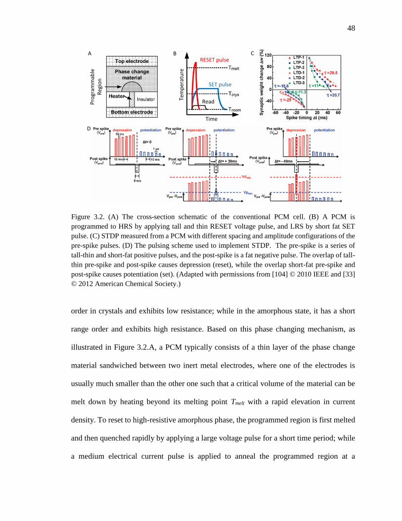
48
order in crystals and exhibits low resistance; while in the amorphous state, it has a short
range order and exhibits high resistance. Based on this phase changing mechanism, as
illustrated in Figure 3.2.A, a PCM typically consists of a thin layer of the phase change
material sandwiched between two inert metal electrodes, where one of the electrodes is
usually much smaller than the other one such that a critical volume of the material can be
melt down by heating beyond its melting point Tmelt with a rapid elevation in current
density. To reset to high-resistive amorphous phase, the programmed region is first melted
and then quenched rapidly by applying a large voltage pulse for a short time period; while
a medium electrical current pulse is applied to anneal the programmed region at a
A B
D
Time
Tem
per
atu
re
Read
SET pulse
RESET pulseC
Pro
gram
mab
le
Reg
ion
Figure 3.2. (A) The cross-section schematic of the conventional PCM cell. (B) A PCM is
programmed to HRS by applying tall and thin RESET voltage pulse, and LRS by short fat SET
pulse. (C) STDP measured from a PCM with different spacing and amplitude configurations of the
pre-spike pulses. (D) The pulsing scheme used to implement STDP. The pre-spike is a series of
tall-thin and short-fat positive pulses, and the post-spike is a fat negative pulse. The overlap of tall-
thin pre-spike and post-spike causes depression (reset), while the overlap short-fat pre-spike and
post-spike causes potentiation (set). (Adapted with permissions from [104] © 2010 IEEE and [33]
© 2012 American Chemical Society.)
49
temperature between the crystallization temperature and the melting temperature Tcrys for
a time period long enough that takes the material to low-resistive crystalline phase. These
program/erase pulse shapes are shown in Figure 3.2.B [104].
PCMs can serve as electronic synapses with STDP learning capability [33], [105],
[106]. Figure 3.2.C shows an STDP implementation in a 200 nm Ge2Sb2Te5 PCM device
[33]. Here, the pre-spike is applied to the top electrode of the PCM the post-spike is applied
to the bottom electrode. The shapes of pre- and post-spikes are different from biological
action potentials: pre-spike is a pulse train that consists of typical tall and thin (10 ns, 50
ns and 100 ns) pulses with increasing amplitudes for depression (reset), and short and fat
(100 ns , 1 μs, and 10 μs) pulses with decreasing amplitudes for potentiation (set). The
post-spike is a 8 ms negative pulse. When the pre- and post-spike overlaps, they create a
net potential over the threshold of 0.36 V for set operation, and the threshold of 0.7 V for
the reset operation. Besides single device evaluation, an application of patttern
recongnition with PCM synapes and STDP learning has been recently demostrated [107].
PCMs have very good endurance, long data retention and are able to achieve
multiple level storage [101]. However, PCMs generally consume more energy than other
nanoscale NVM devices as they solely use Joule heating as their primary mechanism of
state change. PCMs are also relatively larger than other emerging memories. In terms of
STDP learning, PCMs definitely require complicated pulse schema due to their unipolar
switching property; switching depends on the absolute voltage amplitude only and is
independent with the voltage polarity.

50
Spin-Transfer-Torque Random-Access-Memory (STT-RAM)
Spin is an intrinsic binary form of angular momentum carried by electrons.
Generally, an electrical current consists of electrons in either one of the two spin
orientations and the amount of them are same in macroscale statistics. However, by passing
the current through a nanometer scale thin magnetic layer, called fixed layer, a spin-
polarized current with all the electrons spin in the same orientation can be produced. If this
spin-polarized current is directed into a second thinner magnetic layer, called free layer,
angular momentum can be transferred to this layer, and consequently change its magnetic
orientation. Utilizing this spin-transfer-torque effect between fixed and free ferromagnetic
layers, STT-RAM realizes low and high resistance states in a magnetic tunnel junction
(MTJ) with a tunnel barrier layer separating the two ferromagnetic layers, as illustrated in
Figure 3.3.A [108]. When the magnetic direction of the fixed and free layers are parallel
(or aligned in the same direction), the STT-RAM device exhibits low resistance. On the
other hand, when they are anti-parallel (or not aligned in the same direction), the device
A BParallel
Anti-parallel
Free layer
Fixed layer
Tunnelbarrier
Parallel
Anti-parallel
Free layer
Fixed layer
Tunnelbarrier
Figure 3.3. (A) Structure of a magnetic tunnel junction (MJT). The parallel and anti-parallel of the
free layer and fixed layer result LRS and HRS respectively. (B) Resistance increase in a MJT
induced by a stimulus resulting from two sawtooth spikes with a time shift. (Adapted with
permissions from [108] © 2016 IEEE and [109] © 2012 John Wiley and Sons.)

51
exhibits high resistance. During the read operation with a small current, the magnetic
orientation of the free layer is not be disturbed; while in programming operation with a
larger current, the free layer’s orientation will be flipped depending on the current flow
direction.
Some work has been presented in literature to evaluate the use of STT-RAMs as
electronic synapses [109]. Figure 3.3.B demonstrates an increase in STT-RAM resistance
by a net potential over the reset threshold, resulting from the two sawtooth spikes with a
40 seconds time shift [109]. Several experiments also show STT-RAMs behave in a
stochastic fashion. Leveraging the stochastic switching, a vehicle (car) detection task was
simulated in a spiking neural network with STT-RAM synapse [110].
Since STT-RAM drives the state switching by changing the magnetic orientation
in the thin free layer, it is inherently a binary memory device with bipolar switching. STT-
RAM memory is also energy-efficient, with fast switching, and long endurance. However,
the resistance contrast between the two states of the STT-RAM is typically low [111].
Resistive Random-Access-Memory (RRAM)
RRAM devices use the direct resistance change in thin-film insulators to store
information. There are a large number of material systems available to realize the thin-film
insulator. However, RRAM devices can be categorized into several types depending on the
structure of conductive filaments formed in the thin-film insulator. Anion-type RRAM
achieves the resistive switching by the formation of oxygen vacancies and migration of
oxygen-ions. Cation-type RRAM, also known as conductive-bridge RAM (CBRAM),
achieves resistive switching by the formation and dissolution of metal filaments with redox
reaction and migration of metal ions. Oxide-based RRAM relies resistive switching on the
52
conductive filaments consisting of oxygen vacancies, and carbon-based RRAM induces
the resistive switching by hydrogenation and dehydrogenation of hydrogen atoms [112].
Despite different underlying switching physics, all these RRAM devices share a lot of
common device characteristics and the array architecture design considerations are very
similar [113].
Resistance Switching Modes
The most common characteristic of RRAMs is their hysteretic current-voltage
characteristic induced by resistance change occurring between the two stable states, called
the low resistance state (LRS) or ON state and the high resistance state (HRS) or OFF state.
For multilevel operation, intermediate resistance states are utilized as well. A write
operation changing a RRAM from the HRS to the LRS is called a SET operation, while
the opposite write operation changing it from the HRS to the LRS is called a RESET
operation. It should be noted that RRAMs often need an electroforming step prior to their
first write/read operation. This electroforming step generally involves higher current level
than the write/read operations [114], [115].
The operation of resistance change is distinguished by two different modes,
unipolar resistive switching and bipolar resistive switching, as illustrated in Figure 3.4.
Unipolar Switching
The unipolar resistive switching mode is characterized by the fact that the SET and
RESET operations takes place with only one voltage polarity. Changing from the HRS to
the LRS, the SET process takes place at a voltage larger than Vth1, with a LRS current
limited by a current compliance (CC). To change back from the LRS into the HRS, the
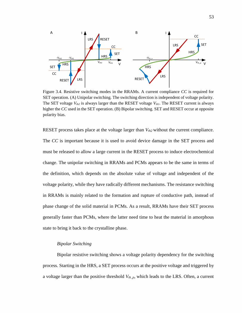
53
RESET process takes place at the voltage larger than Vth2 without the current compliance.
The CC is important because it is used to avoid device damage in the SET process and
must be released to allow a large current in the RESET process to induce electrochemical
change. The unipolar switching in RRAMs and PCMs appears to be the same in terms of
the definition, which depends on the absolute value of voltage and independent of the
voltage polarity, while they have radically different mechanisms. The resistance switching
in RRAMs is mainly related to the formation and rupture of conductive path, instead of
phase change of the solid material in PCMs. As a result, RRAMs have their SET process
generally faster than PCMs, where the latter need time to heat the material in amorphous
state to bring it back to the crystalline phase.
Bipolar Switching
Bipolar resistive switching shows a voltage polarity dependency for the switching
process. Starting in the HRS, a SET process occurs at the positive voltage and triggered by
a voltage larger than the positive threshold Vth_p, which leads to the LRS. Often, a current
A B
RESET
RESET
SET
SET
I I
CC
CC
VV
CC
LRS
LRSLRS
LRS
HRS
HRSHRSSET
RESET
Vth1
-Vth1
HRS
Vth2
-Vth2
Vth_p
-Vth_n
Figure 3.4. Resistive switching modes in the RRAMs. A current compliance CC is required for
SET operation. (A) Unipolar switching. The switching direction is independent of voltage polarity.
The SET voltage Vth2 is always larger than the RESET voltage Vth1. The RESET current is always
higher the CC used in the SET operation. (B) Bipolar switching. SET and RESET occur at opposite
polarity bias.
54
compliance CC is also used to protect the device from damage and determine the resistance
range for LRS. RESET switching process is obtained at a negative voltage. A voltage of
opposite polarity and an amplitude larger than the negative threshold Vth_n is used for the
RESET process to switch the it back into the HRS. Most RRAMs reported in the literature
are operated in the bipolar resistive switching mode.
In both types of switching modes, the resistance states are read out with a voltage
smaller than SET and RESET threshold voltages, while avoiding a detectable change of
the state. Since unipolar switching only uses the voltage amplitudes to perform the
switching, it generally needs a precise control of the voltage applied across the devices,
while bipolar switching has better voltage margins because the SET and RESET operations
are separated by voltage polarity, which also naturally fits into the STDP learning rule and
will be discussed later.
Switching Mechanisms and Operation
Typically, a RRAM device is built as a metal–insulator–metal (MIM) structure
which has a solid electrolyte thin-film inserted between two metal electrodes in a
sandwiched stack. Modern microscopic analysis reveals that the resistive switching in
RRAMs devices involves both physical and chemical processes that take place at different
locations in the devices. Also the electrodes and the insulator layer determine the switching
behavior. In the locational aspect, switching can take place near one of the electrode
interfaces, at the center between the electrode interfaces, or involve the entire path between
the electrode interfaces. A resistive switching can occur in the formation and dissolution
of a single conducting filament, or over the entire cross-section of the device. In the
physical and chemical aspect, the resistive switching can take place due to – (1) the phase
55
change of the material, which is similar to the PCMs, or (2) the conductive filament path
disruption by Joule heating which is a thermo-chemical reaction and similar to fuse-anti-
fuse switching, or (3) valence change of which the migration and accumulation of the
anions, typically oxygen vacancies, around the cathode reduce the valence state of anions
that turning oxide into a metallic phase resulting in the formation of a metallic conductive
channel, or (4) a growth of a metallic conductive filament which is caused by the reduced
metal atoms accumulate at the cathode after metal cations migrate to inert cathode, or (5)
Schottky barrier changing by the trapping of injected electronic charges at the interface of
defect sites. In fact, in a general sense, many of these changes take place concurrently in
the RRAM device and contribute to the resistive switching.
Among various switching mechanisms, the formation and dissolution of a
conductive bridge filament is the one has been intensively studied, and therefore, it is used
as a typical example to illustrate the resistive switching processes in RRAMs. The RRAM
device using metallic conductive bridge filament as the dominant switching mechanism is
called the conductive-bridging RAM (CBRAM).
The sandwich structure of a CBRAM has its anode electrode built with an
electrochemically active metal, e.g. Ag or Cu, the cathode electrode built with an
electrochemically inert metal, e.g. W, Pt or TiN, and the thin film of solid electrolyte
formed by either thermal or photo diffusion of the respective electrochemically active
metal ions into the chalcogenide crystal lattice (called the forming process) [116]. The LRS
of a CBRAM is the state in which a metallic conductive bridge is formed in the ion
conducting amorphous (chalcogenide glass) medium; while HRS is the state where the
metallic conductive bridge is dissolved. The switching between LRS and HRS is triggered
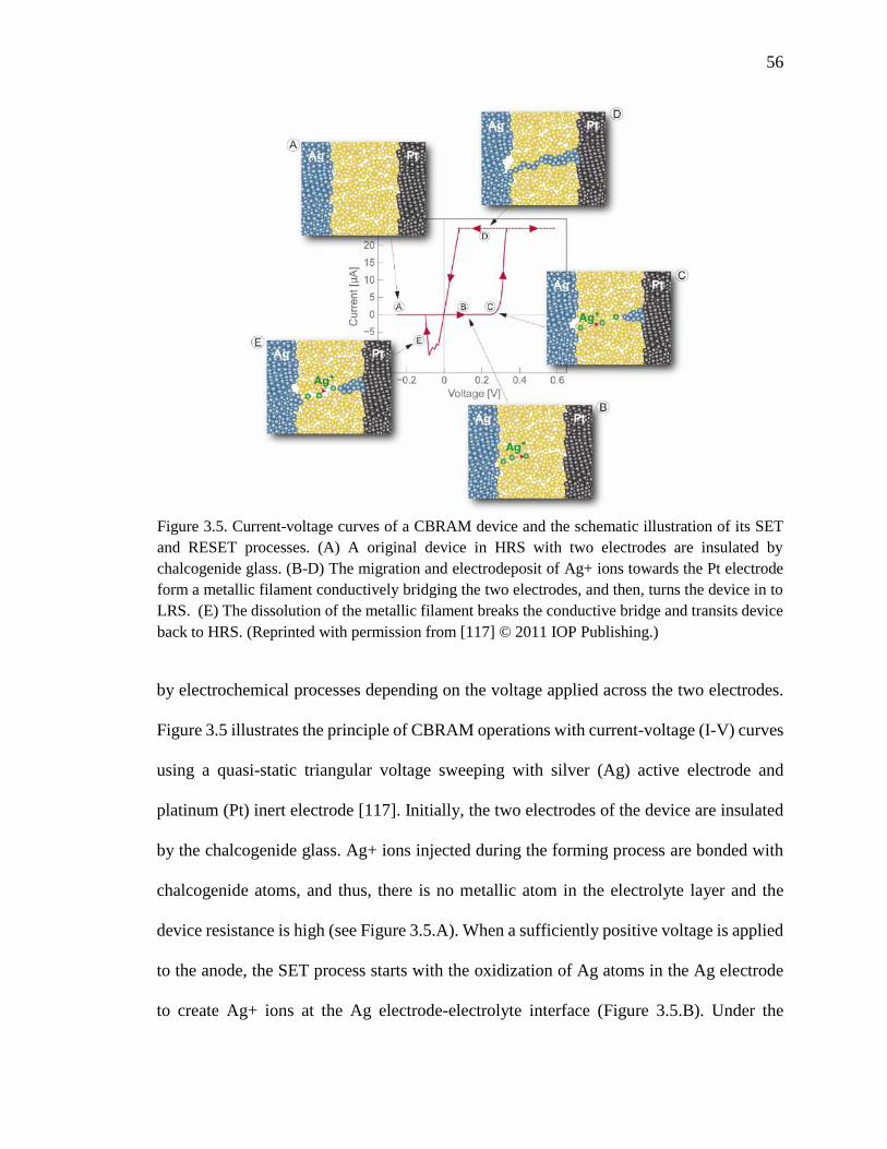
56
by electrochemical processes depending on the voltage applied across the two electrodes.
Figure 3.5 illustrates the principle of CBRAM operations with current-voltage (I-V) curves
using a quasi-static triangular voltage sweeping with silver (Ag) active electrode and
platinum (Pt) inert electrode [117]. Initially, the two electrodes of the device are insulated
by the chalcogenide glass. Ag+ ions injected during the forming process are bonded with
chalcogenide atoms, and thus, there is no metallic atom in the electrolyte layer and the
device resistance is high (see Figure 3.5.A). When a sufficiently positive voltage is applied
to the anode, the SET process starts with the oxidization of Ag atoms in the Ag electrode
to create Ag+ ions at the Ag electrode-electrolyte interface (Figure 3.5.B). Under the
Figure 3.5. Current-voltage curves of a CBRAM device and the schematic illustration of its SET
and RESET processes. (A) A original device in HRS with two electrodes are insulated by
chalcogenide glass. (B-D) The migration and electrodeposit of Ag+ ions towards the Pt electrode
form a metallic filament conductively bridging the two electrodes, and then, turns the device in to
LRS. (E) The dissolution of the metallic filament breaks the conductive bridge and transits device
back to HRS. (Reprinted with permission from [117] © 2011 IOP Publishing.)
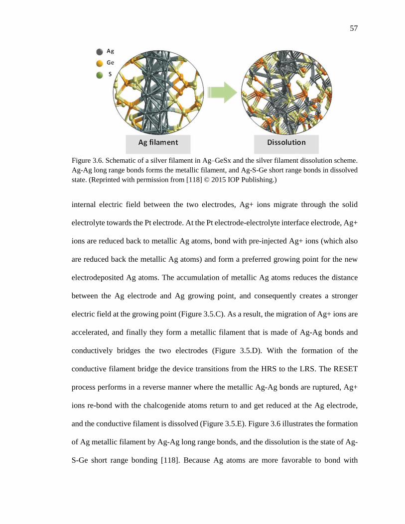
57
internal electric field between the two electrodes, Ag+ ions migrate through the solid
electrolyte towards the Pt electrode. At the Pt electrode-electrolyte interface electrode, Ag+
ions are reduced back to metallic Ag atoms, bond with pre-injected Ag+ ions (which also
are reduced back the metallic Ag atoms) and form a preferred growing point for the new
electrodeposited Ag atoms. The accumulation of metallic Ag atoms reduces the distance
between the Ag electrode and Ag growing point, and consequently creates a stronger
electric field at the growing point (Figure 3.5.C). As a result, the migration of Ag+ ions are
accelerated, and finally they form a metallic filament that is made of Ag-Ag bonds and
conductively bridges the two electrodes (Figure 3.5.D). With the formation of the
conductive filament bridge the device transitions from the HRS to the LRS. The RESET
process performs in a reverse manner where the metallic Ag-Ag bonds are ruptured, Ag+
ions re-bond with the chalcogenide atoms return to and get reduced at the Ag electrode,
and the conductive filament is dissolved (Figure 3.5.E). Figure 3.6 illustrates the formation
of Ag metallic filament by Ag-Ag long range bonds, and the dissolution is the state of Ag-
S-Ge short range bonding [118]. Because Ag atoms are more favorable to bond with
Figure 3.6. Schematic of a silver filament in Ag–GeSx and the silver filament dissolution scheme.
Ag-Ag long range bonds forms the metallic filament, and Ag-S-Ge short range bonds in dissolved
state. (Reprinted with permission from [118] © 2015 IOP Publishing.)

58
chalcogenide atoms, CBRAM appears more stable to stay in HRS than in LRS. This
explains that CBRAMs generally have a relative lower RESET threshold than SET
threshold under small device current [119], and a relative low retention compared to other
nanoscale memory devices.
STDP in Bipolar Switching RRAMs
Many RRAMs are two-terminal bipolar switching devices. A bipolar switching
device has a positive switching threshold voltage Vth_p; the device will change to a lower
resistance state from a high resistance state when the potential applied over the device
larger than Vth_p . The negative threshold voltage -Vth_n dictates that the device will change
to a higher resistance state from a lower resistance state when the potential applied over
the device beyond -Vth_n. A very important consequence of bipolar resistive switching is
that a STDP learning scheme equivalent to the biological synapse can be realized in situ
just by overlapping two simple voltage waveforms across this two-terminal passive device,
as elaborated in Figure 3.7. Here two voltage waveforms Vpre (called pre-synaptic spike)
and Vpost (called post-synaptic spike) are applied at the opposite terminals of the bipolar
resistive switching device. The voltage waveform of Vpre and Vpost is designed to
individually have two opposite polarities separated in time, i.e. with positive and negative
excursions as shown in Figure 3.7. The peak amplitudes of these two parts, Va+ and Va-,
are smaller than the positive threshold and negative threshold respectively
𝑉𝑎+ < 𝑉𝑡ℎ_𝑝
𝑉𝑎− < 𝑉𝑡ℎ_𝑛.
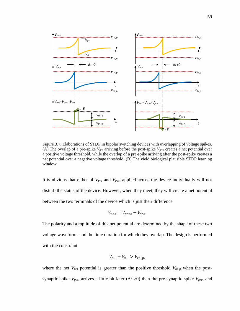
59
It is obvious that either of Vpre and Vpost applied across the device individually will not
disturb the status of the device. However, when they meet, they will create a net potential
between the two terminals of the device which is just their difference
𝑉𝑛𝑒𝑡 = 𝑉𝑝𝑜𝑠𝑡 − 𝑉𝑝𝑟𝑒.
The polarity and a mplitude of this net potential are determined by the shape of these two
voltage waveforms and the time duration for which they overlap. The design is performed
with the constraint
𝑉𝑎+ + 𝑉𝑎− > 𝑉𝑡ℎ_𝑝,
where the net Vnet potential is greater than the positive threshold Vth_p when the post-
synaptic spike Vpost arrives a little bit later (Δt >0) than the pre-synaptic spike Vpre, and
t
t
t
vth_p
vth_n
Vpost
VpreΔt>0
Vnet=Vpost-Vpre
t
Vpost
VpreΔt<0
Vnet=Vpost-Vpre
vth_p
vth_n
t
vth_p
vth_p
t
vth_n
vth_n
vth_p
vth_p
vth_n
vth_n
Va+
Va-
E
E
Figure 3.7. Elaborations of STDP in bipolar switching devices with overlapping of voltage spikes.
(A) The overlap of a pre-spike Vpre arriving before the post-spike Vpost creates a net potential over
a positive voltage threshold, while the overlap of a pre-spike arriving after the post-spike creates a
net potential over a negative voltage threshold. (B) The yield biological plausible STDP learning
window.
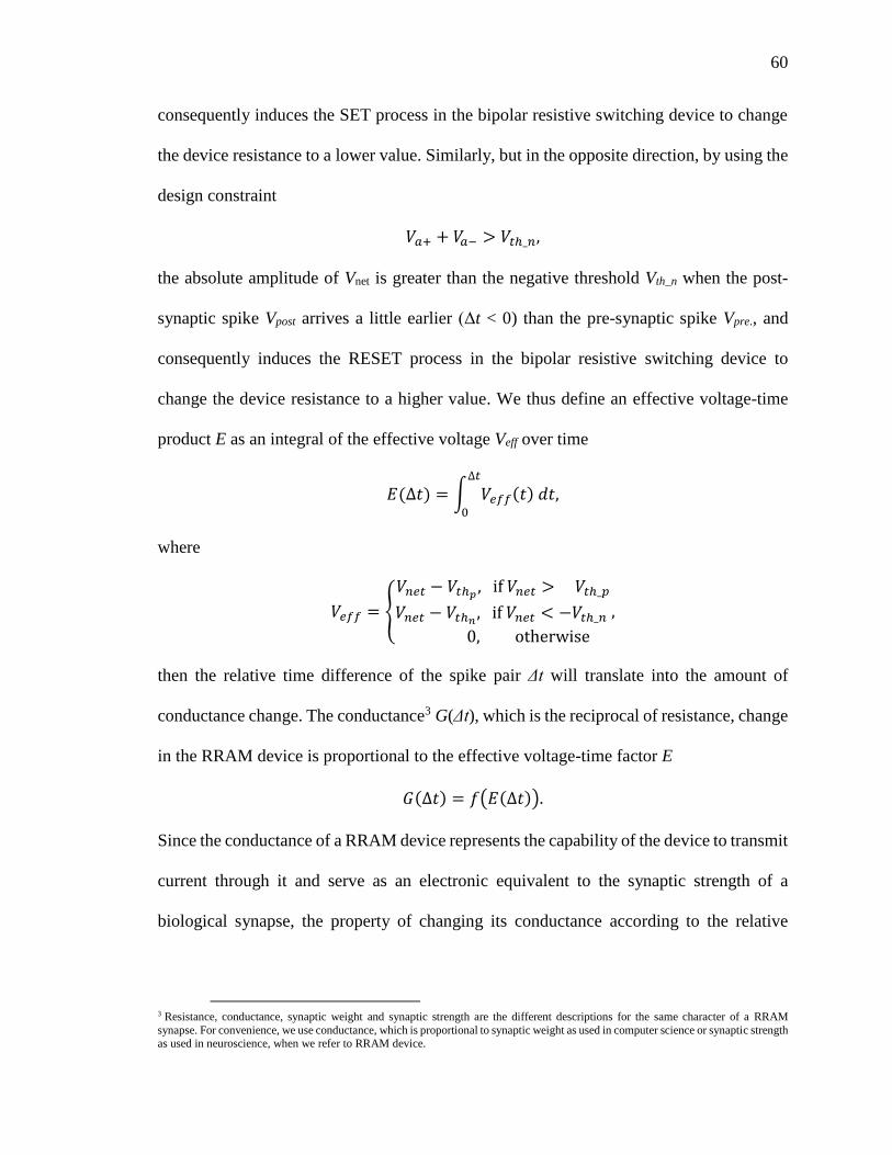
60
consequently induces the SET process in the bipolar resistive switching device to change
the device resistance to a lower value. Similarly, but in the opposite direction, by using the
design constraint
𝑉𝑎+ + 𝑉𝑎− > 𝑉𝑡ℎ_𝑛,
the absolute amplitude of Vnet is greater than the negative threshold Vth_n when the post-
synaptic spike Vpost arrives a little earlier (Δt < 0) than the pre-synaptic spike Vpre., and
consequently induces the RESET process in the bipolar resistive switching device to
change the device resistance to a higher value. We thus define an effective voltage-time
product E as an integral of the effective voltage Veff over time
𝐸(∆𝑡) = ∫ 𝑉𝑒𝑓𝑓(𝑡) 𝑑𝑡,∆𝑡
0
where
𝑉𝑒𝑓𝑓 =
𝑉𝑛𝑒𝑡 − 𝑉𝑡ℎ𝑝, if 𝑉𝑛𝑒𝑡 > 𝑉𝑡ℎ_𝑝
𝑉𝑛𝑒𝑡 − 𝑉𝑡ℎ𝑛, if 𝑉𝑛𝑒𝑡 < −𝑉𝑡ℎ_𝑛
0, otherwise
,
then the relative time difference of the spike pair Δt will translate into the amount of
conductance change. The conductance3 G(Δt), which is the reciprocal of resistance, change
in the RRAM device is proportional to the effective voltage-time factor E
𝐺(∆𝑡) = 𝑓(𝐸(∆𝑡)).
Since the conductance of a RRAM device represents the capability of the device to transmit
current through it and serve as an electronic equivalent to the synaptic strength of a
biological synapse, the property of changing its conductance according to the relative
3 Resistance, conductance, synaptic weight and synaptic strength are the different descriptions for the same character of a RRAM
synapse. For convenience, we use conductance, which is proportional to synaptic weight as used in computer science or synaptic strength as used in neuroscience, when we refer to RRAM device.
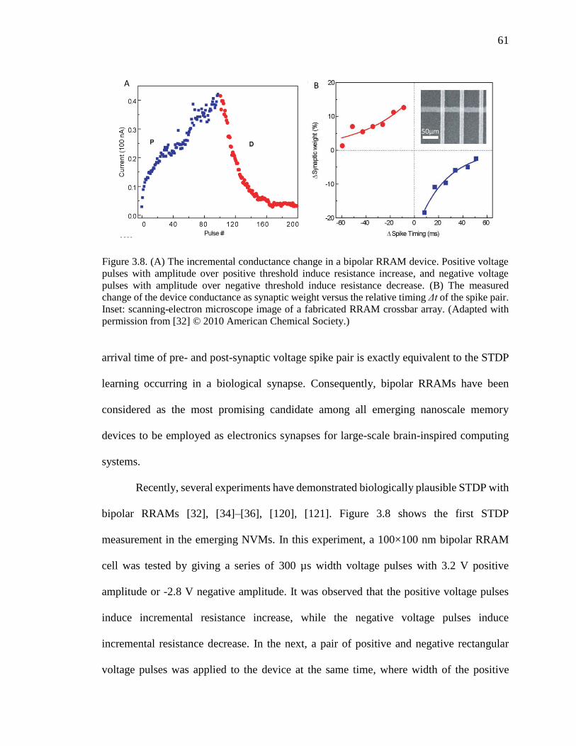
61
arrival time of pre- and post-synaptic voltage spike pair is exactly equivalent to the STDP
learning occurring in a biological synapse. Consequently, bipolar RRAMs have been
considered as the most promising candidate among all emerging nanoscale memory
devices to be employed as electronics synapses for large-scale brain-inspired computing
systems.
Recently, several experiments have demonstrated biologically plausible STDP with
bipolar RRAMs [32], [34]–[36], [120], [121]. Figure 3.8 shows the first STDP
measurement in the emerging NVMs. In this experiment, a 100×100 nm bipolar RRAM
cell was tested by giving a series of 300 µs width voltage pulses with 3.2 V positive
amplitude or -2.8 V negative amplitude. It was observed that the positive voltage pulses
induce incremental resistance increase, while the negative voltage pulses induce
incremental resistance decrease. In the next, a pair of positive and negative rectangular
voltage pulses was applied to the device at the same time, where width of the positive
A B
50µm
Figure 3.8. (A) The incremental conductance change in a bipolar RRAM device. Positive voltage
pulses with amplitude over positive threshold induce resistance increase, and negative voltage
pulses with amplitude over negative threshold induce resistance decrease. (B) The measured
change of the device conductance as synaptic weight versus the relative timing Δt of the spike pair.
Inset: scanning-electron microscope image of a fabricated RRAM crossbar array. (Adapted with
permission from [32] © 2010 American Chemical Society.)
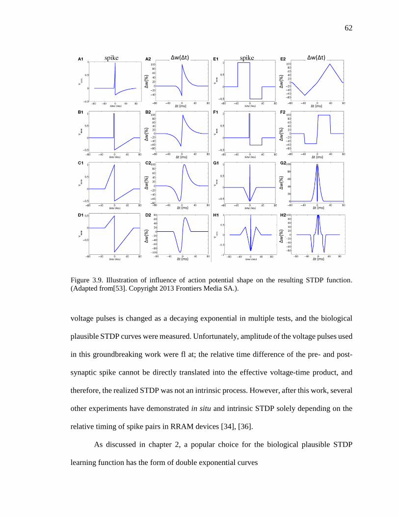
62
voltage pulses is changed as a decaying exponential in multiple tests, and the biological
plausible STDP curves were measured. Unfortunately, amplitude of the voltage pulses used
in this groundbreaking work were fl at; the relative time difference of the pre- and post-
synaptic spike cannot be directly translated into the effective voltage-time product, and
therefore, the realized STDP was not an intrinsic process. However, after this work, several
other experiments have demonstrated in situ and intrinsic STDP solely depending on the
relative timing of spike pairs in RRAM devices [34], [36].
As discussed in chapter 2, a popular choice for the biological plausible STDP
learning function has the form of double exponential curves
Δw(Δt) Δw(Δt)
Δt (ms) Δt (ms)
Δt (ms) Δt (ms)
Δt (ms) Δt (ms)
Δt (ms) Δt (ms)
Δw
(%)
Δw
(%)
Δw
(%)
Δw
(%)
Δw
(%)
Δw
(%)
Δw
(%)
Δw
(%)
Figure 3.9. Illustration of influence of action potential shape on the resulting STDP function.
(Adapted from[53]. Copyright 2013 Frontiers Media SA.).
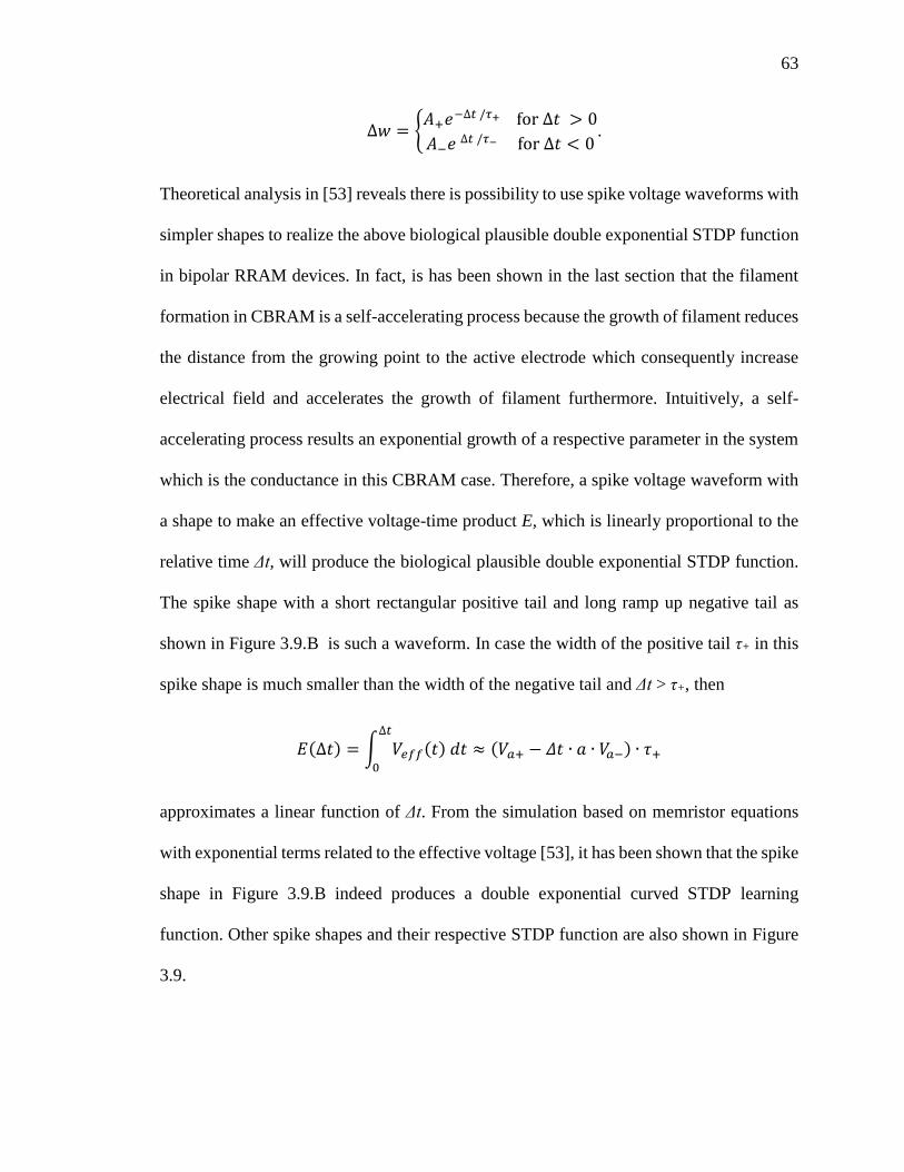
63
∆𝑤 = 𝐴+𝑒−∆𝑡 /𝜏+ for ∆𝑡 > 0
𝐴−𝑒 ∆𝑡 /𝜏− for ∆𝑡 < 0.
Theoretical analysis in [53] reveals there is possibility to use spike voltage waveforms with
simpler shapes to realize the above biological plausible double exponential STDP function
in bipolar RRAM devices. In fact, is has been shown in the last section that the filament
formation in CBRAM is a self-accelerating process because the growth of filament reduces
the distance from the growing point to the active electrode which consequently increase
electrical field and accelerates the growth of filament furthermore. Intuitively, a self-
accelerating process results an exponential growth of a respective parameter in the system
which is the conductance in this CBRAM case. Therefore, a spike voltage waveform with
a shape to make an effective voltage-time product E, which is linearly proportional to the
relative time Δt, will produce the biological plausible double exponential STDP function.
The spike shape with a short rectangular positive tail and long ramp up negative tail as
shown in Figure 3.9.B is such a waveform. In case the width of the positive tail τ+ in this
spike shape is much smaller than the width of the negative tail and Δt > τ+, then
𝐸(∆𝑡) = ∫ 𝑉𝑒𝑓𝑓(𝑡) 𝑑𝑡∆𝑡
0
≈ (𝑉𝑎+ − 𝛥𝑡 ∙ 𝑎 ∙ 𝑉𝑎−) ∙ 𝜏+
approximates a linear function of Δt. From the simulation based on memristor equations
with exponential terms related to the effective voltage [53], it has been shown that the spike
shape in Figure 3.9.B indeed produces a double exponential curved STDP learning
function. Other spike shapes and their respective STDP function are also shown in Figure
3.9.
64
Device Characteristics for Neuromorphic Computing
When considering the use of emerging NVMs as electrical synaptic devices, some
of basic device characteristics, including energy efficiency, size, retention and endurance,
need to be evaluated.
Energy Efficiency
The projected unsustainable energy consumption as discussed in Chapter 1 is the
primary motivation to pursue brain-inspired computing systems. Thus, among all
performance metrics, energy-efficiency is the primary consideration to select or custom
design a nanoscale memory device for potential neuromorphic applications. Since such a
memory doesn’t need static power to retain its state, NVM has zero standby energy
consumption. While the read operation can be much shorter and requires smaller voltage
than the write, the energy efficiency of a two-terminal memory device is determined by the
current, speed and voltage used during a write read operation. Considering the potential
integration with modern CMOS technology, the write voltage is in a relatively small range
from 0.5 V to 3V, which is desirable. So far, the reported write speed of major STT-RAM
test chips ranges from 1 ns to 100 ns, RRAMs ranges from 10 ns to 100 ns, and PCMs
ranges from 100 ns to 1 µs [101]. While the write current has been improved a lot in past
several years and can be brought under 100 µA. Taking 10 ns writing speed as the
reference, the present NVMs could achieve energy consumption at the magnitude of 10-12
J (or 1 pJ) per switch. Comparing to a synapse in the human brain which consumes about
2×10-15 J (or 2 fJ) to transmit one bit information (equivalent to 25,000 ATP [122], [123]),
nanoscale NVMs is promising in ultimately achieving a similar energy efficiency, while
the key is the realizing of a lower write current or faster write speed. For instance, a device
65
with the properties of 1 µA write current and 1 ns write speed [124] can result a comparable
energy efficiency to biological synapses.
Device Dimensions
We have discussed that a meaningful brain-inspired computing system requires a
large-scale integration of neural network, therefore, a compact memory device with small
footprint is desired. As the density has been a fundamental requirement for a memory
technology, the mainstream emerging NVMs have been designed to be two-terminal,
occupying 4 F2 size, and exhibit the potential to be scaled down to nanometer regime.
Moreover, the 3D integration of emerging NVMs have been demonstrated [125]–[127] and
will continue to evolve rapidly. Referring to the 300 nm diameter of synaptic active zone
[128] (equivalent to the diameter of memory device) and 20 nm width of the synaptic cleft
(equivalent to the thickness of memory device ), it is very promising to achieve a synaptic
density with NVM synapses that comparable to the human brain.
Resolution
Mathematical analysis also shows synaptic learning prefers precise weight state
(see PCA implication of Hebbian learning in the previous chapter). There are some
experiments that have demonstrated multi-level NVMs, however, these implementations
require relative large devices [129], or the intermediate states do not last long (i.e. they
relax to more stable states, often showing bistable behavior). Most of nanoscale memory
devices exhibit behaviors of both binary switching and stochastic switching in nanometer
regime [119], [124], [130]–[133]. One of the solution is to use compound binary devices
which employ several devices in parallel [52], [133], which in fact is equivalent to a larger
66
area device in some sense. Simulations in [52] show a compound device with 10 binary
devices in parallel (or 3.3-bits equivalent) allows reasonable performance in a pattern
recognition task with little accuracy degradation when compared to the one using 100
devices in parallel (6.6-bits). Interestingly, the synaptic transmission and synaptic plasticity
in biological synapses is a stochastic process through multiple NMDA receptors, and the
typical number of these receptors is 20 (or 4.3-bit) [128]. Taking 4-bits as a target for 160
nm compound device, this means a 5 nm for an individual binary device. The research of
computing with stochastic synapses remains fairly recent, and more work is required to be
done to understand the impact on applications and the trade-off among other design
parameters.
Retention and Endurance
For a general purpose computing system, 10-years data retention and system
endurance may be required. With 4 Hz operation frequency similar to the brain synapses
[123], this translates to an endurance of 1×10⁹ write operations, which is the upper limit of
the most emerging NVMs [101]. However, considering that a practical neuromorphic
system needs much faster learning speed than human beings which spans years, the
endurance of memory devices for brain-inspired computing need to be improved
significantly. Taking a learning of MNIST dataset as an example, if the system was
expected to learn 60,000 training samples with 10 epochs every day, the synaptic operation
frequency increases to 166 Hz, and then the 10-years endurance specification becomes
4.7×10¹⁰. Conversely, if the expectation is 1 second, the synaptic operation frequency
increase to 100 kHz, and then the 10-years endurance specification skyrockets to 1.5×10¹⁴.
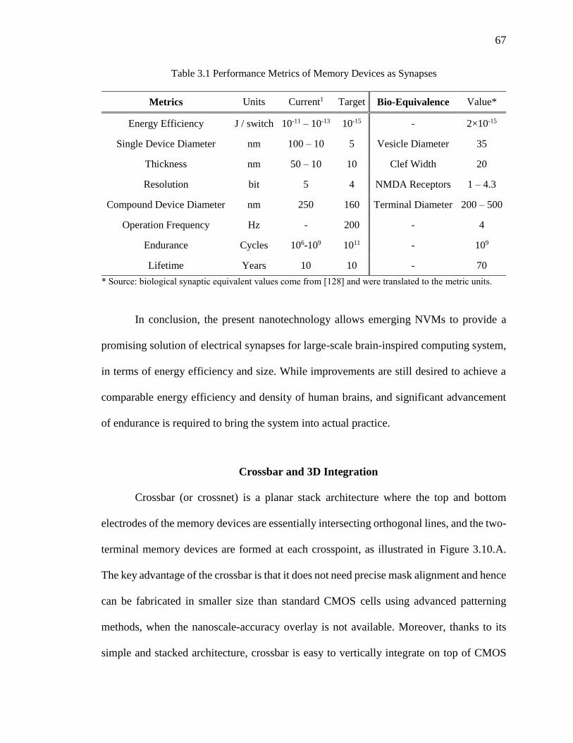
67
In conclusion, the present nanotechnology allows emerging NVMs to provide a
promising solution of electrical synapses for large-scale brain-inspired computing system,
in terms of energy efficiency and size. While improvements are still desired to achieve a
comparable energy efficiency and density of human brains, and significant advancement
of endurance is required to bring the system into actual practice.
Crossbar and 3D Integration
Crossbar (or crossnet) is a planar stack architecture where the top and bottom
electrodes of the memory devices are essentially intersecting orthogonal lines, and the two-
terminal memory devices are formed at each crosspoint, as illustrated in Figure 3.10.A.
The key advantage of the crossbar is that it does not need precise mask alignment and hence
can be fabricated in smaller size than standard CMOS cells using advanced patterning
methods, when the nanoscale-accuracy overlay is not available. Moreover, thanks to its
simple and stacked architecture, crossbar is easy to vertically integrate on top of CMOS
Table 3.1 Performance Metrics of Memory Devices as Synapses
Metrics Units Current1 Target Bio-Equivalence Value*
Energy Efficiency J / switch 10-11 – 10-13 10-15 - 2×10-15
Single Device Diameter nm 100 – 10 5 Vesicle Diameter 35
Thickness nm 50 – 10 10 Clef Width 20
Resolution bit 5 4 NMDA Receptors 1 – 4.3
Compound Device Diameter nm 250 160 Terminal Diameter 200 – 500
Operation Frequency Hz - 200 - 4
Endurance Cycles 106-109 1011 - 109
Lifetime Years 10 10 - 70
* Source: biological synaptic equivalent values come from [128] and were translated to the metric units.

68
subsystem circuits, as an add-on in the back-end-of-the-line (BEOL) of the CMOS process
[134]. In the vertical integration, as illustrated in Figure 3.10.B, the bottom electrode wires
of the crossbar can connect to the underneath CMOS system with metal-via-metal contacts
directly, while the connections of the top electrode wires and CMOS system need to use
through via silicon (TSV) technology [135]. This allows the CMOS system to address
every top/bottom electrode wire, and therefore address every memory device at the
crosspoint of the add-on crossbar. By employing crosspoint memory devices as synapse
via
A B
Metal plane electrodeMetal pillarelectrode
Memory cell
VerticalMOSFET
CommonSource / Drain
CommonGate
C
via TSV
metal layer of CMOS system
Crosspoint Interface pins
Nanowire
CMOS
Bottom electrode wires
Top ele
ctro
de wire
s
Similar two-terminalnanodevices at eachcrosspoint
Figure 3.10. Crossbar architecture and 3D integration. (A) Memory devices organized between
intersecting orthogonal crossbars. (B) Cross-section illustration of the integration of crossbar on
top pf CMOS circuits with interconnection through standard vias and TSVs. (C) Schematic of 3D
crosspoint architecture using the vertical RRAM cells and vertical MOSFETs. (Adapted with
permission [114] © 2013 American Chemical Society).
69
and the top/bottom crossbar wires as passive dendrite trees and axons, the crossbar
architecture provides an effective connectivity solution to large-scale hybrid
CMOS/RRAM network for brain-inspired, or neuromorphic, computing system.
Standalone planar crossbar architectures have been employed and demonstrated in
many nanoscale memories, and multilayer crossbar devices were also demonstrated
recently [125], [136]. With the CMOS device moving to vertical structure (known as
FinFET) in nanometer regime, vertical sandwiched crossbars were also proposed [137].
The vertical crossbar can be built with pillar electrodes and multilayer plane electrodes,
which requires only one critical lithography mask, and hence more promising for higher
density, better integration with CMOS, and lower cost. An example of 3D crossbar
architecture using the vertical RRAM cells and vertical MOSFETs is depict in Figure
3.10.C. Here, the vertical metal pillar electrodes build the frame of a 3D structure. The
RRAM cells are formed between the pillar electrodes and multilayer metal plane electrodes
as a vertical surrounding wall. The metal pillar electrodes extend downwards to connect
with the CMOS circuits which can be in planar fashion or in vertical fashion as well. The
metal plane electrodes are able to connect to the underneath CMOS circuits by TSVs or
laterally connect to other 3D structure on the same substrate. Vertical integration of CMOS
substrate and multiplayer RRAM crossbars unleashes the potential to connect a large
number of synapses with CMOS neurons, thus, is promising to achieve a comparable
density to human brains in terms of geometric dimension. In conjunction with potential
lateral placement of 3D chips and vertical stacks of chips, large-scale deep neural network
with hybrid CMOS / RRAM technology appear to be feasible.
70
Summary
In this chapter, the emerging NVM technologies were briefly introduced. Dedicated
introduction was provided for the PCM, STT-RAM and RRAM devices, which are all two-
terminal nanoscale memories. These devices enable dense integration in a crossbar
architecture, store and represent information in resistance values, and have demonstrated
STDP capability. Specially, RRAM devices allow bipolar resistive switching and
potentially multi-level resistive states, therefore, can realize in situ biological plausible
STDP function by using simple voltage waveforms as pre- and post-synaptic spikes. Then,
the relationship between the spike waveform shape and the respective STDP function was
discussed. By matching the potential system specifications of a brain-inspired computing
system to human brains characteristics, the requirements of energy efficiency, size,
resolution, retention and endurance to memory devices were reviewed and summarized,
where energy efficiency and the endurance may be the most challenging characteristics and
may need significant improvement in the future development of memory devices as
electronic synapses. Finally, the details of crossbar architectures and further vertical
integration possibilities were presented. In conclusion, the state-of-art nanotechnology
provides a very promising solution to use memory device as dense synapses together with
modern CMOS technology. The hybrid integration of multilayer RRAM crossbar and
CMOS neurons paves a path for realizing large-scale brain-inspired hardware with
comparable energy-efficiency, real-time processing capability, and compact 3D volume to
the wetware, i.e. the human brain.
71
CHAPTER 4
INTRODUCTION TO BUILDING BLOCKS OF ANALOG SPIKING
NEURONS
Neuron is the core component in a neural network that connects all the elements
together to perform learning and computation. There are many different types of neurons
in biological brains. While most of them share the common attributes: accumulate inputs
from the sensory afferents or adjunctive neurons, compete with other neurons to generate
spikes, propagate spikes, and modulate synaptic strength with relative timing of spikes.
There have been many design approaches for silicon neurons to implement these
functionalities with different emphasis on biological fidelity, complexity and efficiency.
This chapter reviews the major building blocks required for analog spiking neuron designs
along with several significant implantations of silicon neurons.
Spatio-Temporal Integration
Information processing in a neuron starts from the spatial and temporal current
summation. The accumulated charge is stored in the cell body of a biological neuron, of
which the membrane acts the dielectric of an equivalent capacitor. To mimic this behavior,
the spatiotemporal integration is usually realized using an on-chip capacitor in
neuromorphic circuits.
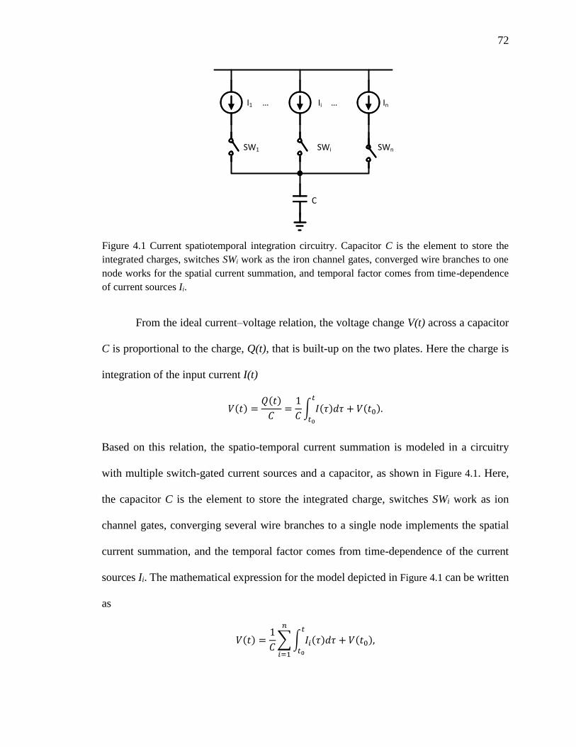
72
From the ideal current–voltage relation, the voltage change V(t) across a capacitor
C is proportional to the charge, Q(t), that is built-up on the two plates. Here the charge is
integration of the input current I(t)
𝑉(𝑡) =𝑄(𝑡)
𝐶=
1
𝐶∫ 𝐼(𝜏)𝑑𝜏
𝑡
𝑡0
+ 𝑉(𝑡0).
Based on this relation, the spatio-temporal current summation is modeled in a circuitry
with multiple switch-gated current sources and a capacitor, as shown in Figure 4.1. Here,
the capacitor C is the element to store the integrated charge, switches SWi work as ion
channel gates, converging several wire branches to a single node implements the spatial
current summation, and the temporal factor comes from time-dependence of the current
sources Ii. The mathematical expression for the model depicted in Figure 4.1 can be written
as
𝑉(𝑡) =1
𝐶∑ ∫ 𝐼𝑖(𝜏)𝑑𝜏
𝑡
𝑡0
𝑛
𝑖=1
+ 𝑉(𝑡0),
C
I1 In
SW1 SWn
Ii
SWi
Figure 4.1 Current spatiotemporal integration circuitry. Capacitor C is the element to store the
integrated charges, switches SWi work as the iron channel gates, converged wire branches to one
node works for the spatial current summation, and temporal factor comes from time-dependence
of current sources Ii.

73
where the integral term presents the temporal integration, and the summation term
presents the spatial integration.
Passive Integrators
The simplest implementation of a current integrator is the follower-integrator. It
can be implemented even with a single MOSFET, of which the channel current is
controlled by the transistor’s gate voltage as shown in Figure 4.2. It consists of a voltage-
controlled PMOS activated by a brief active-low spike with its output node connected to a
capacitor. When a spike reaches the transistor, a post-synaptic current flows from the power
supply, integrates on the capacitor and yields the membrane voltage Vmem; the transistor is
off for the rest of the time. The amount of current ID is controlled by the voltage level of
the spike, and is usually set to a small value by biasing the transistor in sub-threshold region
of operation which can be formulated as
𝐼𝐷(𝑡) = 𝐼𝐷0
𝑊
𝐿𝑒
−1
𝑛𝑉𝑇(𝑉𝑠𝑝𝑘(𝑡)−𝑉𝐷𝐷)
,
where Vdd is the supply voltage, Vspk is the input spike voltage, W and L are the transistor’s
width and length, ID0 is the leakage current, n is a nonlinearity factor, and VT is the thermal
voltage. By connecting multiple MOSFET branches into a tree shape, the circuit realizes a
simple spatio-temporal integration, and can form a silicon neuron circuit that model
sodium, potassium, and other ion channel dynamics in a faithful way [138]. The follower
integrator circuit is extremely compact, but is difficult to control and tune its characteristics
which depend on implicit device parameters, e.g. leakage depends on parallel resistance
and off current of the MOSFET. Finally, as a passive integrator, the increase of Vmem
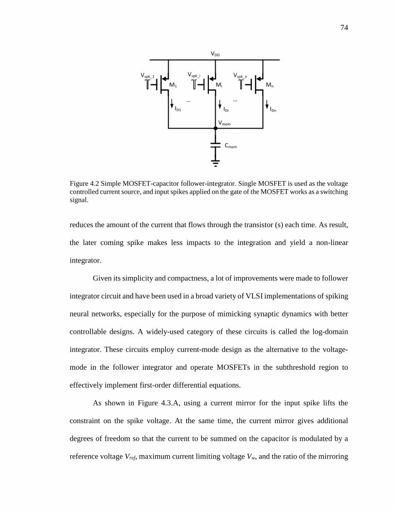
74
reduces the amount of the current that flows through the transistor (s) each time. As result,
the later coming spike makes less impacts to the integration and yield a non-linear
integrator.
Given its simplicity and compactness, a lot of improvements were made to follower
integrator circuit and have been used in a broad variety of VLSI implementations of spiking
neural networks, especially for the purpose of mimicking synaptic dynamics with better
controllable designs. A widely-used category of these circuits is called the log-domain
integrator. These circuits employ current-mode design as the alternative to the voltage-
mode in the follower integrator and operate MOSFETs in the subthreshold region to
effectively implement first-order differential equations.
As shown in Figure 4.3.A, using a current mirror for the input spike lifts the
constraint on the spike voltage. At the same time, the current mirror gives additional
degrees of freedom so that the current to be summed on the capacitor is modulated by a
reference voltage Vref, maximum current limiting voltage Vw, and the ratio of the mirroring
Cmem
M1 MnMi
Vmem
VDD
Vspk_1 Vspk_i Vspk_n
ID1 IDi IDn
Figure 4.2 Simple MOSFET-capacitor follower-integrator. Single MOSFET is used as the voltage
controlled current source, and input spikes applied on the gate of the MOSFET works as a switching
signal.
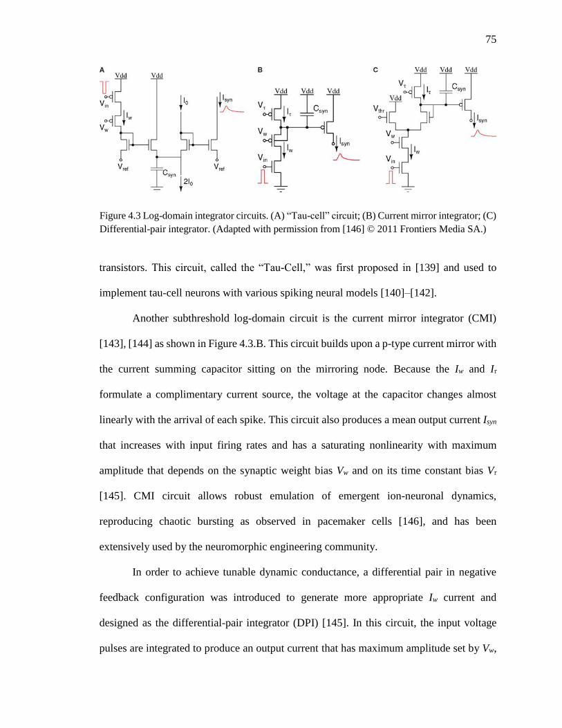
75
transistors. This circuit, called the “Tau-Cell,” was first proposed in [139] and used to
implement tau-cell neurons with various spiking neural models [140]–[142].
Another subthreshold log-domain circuit is the current mirror integrator (CMI)
[143], [144] as shown in Figure 4.3.B. This circuit builds upon a p-type current mirror with
the current summing capacitor sitting on the mirroring node. Because the Iw and Iτ
formulate a complimentary current source, the voltage at the capacitor changes almost
linearly with the arrival of each spike. This circuit also produces a mean output current Isyn
that increases with input firing rates and has a saturating nonlinearity with maximum
amplitude that depends on the synaptic weight bias Vw and on its time constant bias Vτ
[145]. CMI circuit allows robust emulation of emergent ion-neuronal dynamics,
reproducing chaotic bursting as observed in pacemaker cells [146], and has been
extensively used by the neuromorphic engineering community.
In order to achieve tunable dynamic conductance, a differential pair in negative
feedback configuration was introduced to generate more appropriate Iw current and
designed as the differential-pair integrator (DPI) [145]. In this circuit, the input voltage
pulses are integrated to produce an output current that has maximum amplitude set by Vw,
Figure 4.3 Log-domain integrator circuits. (A) “Tau-cell” circuit; (B) Current mirror integrator; (C)
Differential-pair integrator. (Adapted with permission from [146] © 2011 Frontiers Media SA.)
76
Vt, and Vthr. Here, Vthr bias offers an extra degree of freedom via to implement additional
adaptation and plasticity schemes. DPI enables generalized silicon implementations of LIF
neuron [147] and has been used to build a small-scale spiking neuromorphic processor
[148].
Passive integrators are generally compact in silicon area and very energy-efficient
when biased appropriately in the subthreshold region. With these advantages, they are
widely used in the implementation of silicon synapses [145], [149] and forge silicon
neurons that are able to faithfully model the ionic channel dynamics in biological spiking
neurons. However, synapse acts as a controllable current source in these circuits, therefore
consume large silicon area and are not amenable for large-scale neuromorphic networks
when the number of synapses is large.
Leveraging the DPI architecture, a circuit to integrate a dense array of two-terminal
memristors was proposed in [41]. The major challenge of this circuit is that it fails to
provide stable voltage on the node of current integration. Therefore, it is difficult to control
the potential across RRAM synaptic devices to be under the threshold voltage when no
synapse change is expected, while exceeding the thresholds during STDP. As a result, it
cannot utilize the STDP property offered by the RRAM nano-device and then, in fact, not
really works for dense RRAM integration. However, this circuit is useful to produce the
same and shared post-synaptic temporal dynamics or connecting to active synapses which
are formed around nano STT-RAM device [150].
Opamp Integrators
Precise and linear current integrator can be built with operational amplifiers
(opamp). A standard opamp is a voltage amplifier with a differential input and a single-
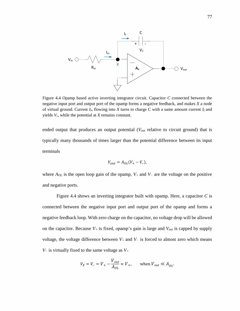
77
ended output that produces an output potential (Vout relative to circuit ground) that is
typically many thousands of times larger than the potential difference between its input
terminals
𝑉𝑜𝑢𝑡 = 𝐴𝑂𝐿(𝑉+ − 𝑉−),
where AOL is the open loop gain of the opamp, V+ and V− are the voltage on the positive
and negative ports.
Figure 4.4 shows an inverting integrator built with opamp. Here, a capacitor C is
connected between the negative input port and output port of the opamp and forms a
negative feedback loop. With zero charge on the capacitor, no voltage drop will be allowed
on the capacitor. Because V+ is fixed, opamp’s gain is large and Vout is capped by supply
voltage, the voltage difference between V+ and V− is forced to almost zero which means
V− is virtually fixed to the same voltage as V+
𝑉𝑋 = 𝑉− = 𝑉+ −𝑉𝑜𝑢𝑡
𝐴𝑂𝐿≈ 𝑉+, when 𝑉𝑜𝑢𝑡 ≪ 𝐴𝑂𝐿.
C
Iin
VoutAvAv
X
If
Rin
Vin
VC
+ -
Figure 4.4 Opamp based active inverting integrator circuit. Capacitor C connected between the
negative input port and output port of the opamp forms a negative feedback, and makes X a node
of virtual ground. Current Iin flowing into X turns to charge C with a same amount current If and
yields Vc, while the potential at X remains constant.
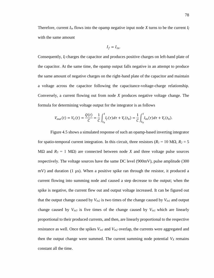
78
Therefore, current Iin flows into the opamp negative input node X turns to be the current If
with the same amount
𝐼𝑓 = 𝐼𝑖𝑛.
Consequently, If charges the capacitor and produces positive charges on left-hand plate of
the capacitor. At the same time, the opamp output falls negative in an attempt to produce
the same amount of negative charges on the right-hand plate of the capacitor and maintain
a voltage across the capacitor following the capacitance-voltage-charge relationship.
Conversely, a current flowing out from node X produces negative voltage change. The
formula for determining voltage output for the integrator is as follows
𝑉𝑜𝑢𝑡(𝑡) = 𝑉𝐶(𝑡) =𝑄(𝑡)
𝐶=
1
𝐶∫ 𝐼𝑓(𝜏)𝑑𝜏
𝑡
𝑡0
+ 𝑉𝑐(𝑡0) =1
𝐶∫ 𝐼𝑖𝑛(𝜏)𝑑𝜏
𝑡
𝑡0
+ 𝑉𝑐(𝑡0).
Figure 4.5 shows a simulated response of such an opamp-based inverting integrator
for spatio-temporal current integration. In this circuit, three resistors (R1 = 10 MΩ, R2 = 5
MΩ and R3 = 1 MΩ) are connected between node X and three voltage pulse sources
respectively. The voltage sources have the same DC level (900mV), pulse amplitude (300
mV) and duration (1 µs). When a positive spike ran through the resistor, it produced a
current flowing into summing node and caused a step decrease to the output; when the
spike is negative, the current flew out and output voltage increased. It can be figured out
that the output change caused by Vin2 is two times of the change caused by Vin1 and output
change caused by Vin3 is five times of the change caused by Vin1 which are linearly
proportional to their produced currents, and then, are linearly proportional to the respective
resistance as well. Once the spikes Vin1 and Vin2 overlap, the currents were aggregated and
then the output change were summed. The current summing node potential VX remains
constant all the time.
79
As a conclusion, the opamp-based inverting integrator provides a current summing
node X which has a constant voltage level and is a very important attribute to enable reliable
interfacing with RRAM devices. Moreover, opamp integrator is a linear current integrator,
because its output node is isolated from the current summing node which has been fixed
Figure 4.5 Response of opamp-based inverting integrator. These pulses cause step decrease and
increase to the output voltage Vout. The step size is linearly proportional to the amount of current,
and the direction of change depends on the current flow direction. The effect of current aggregation
occurs when spikes Vin1 and Vin2 overlap. The current summing node potential VX remains constant
during the integration.
80
and doesn’t move with charge accumulation on the capacitor. This also makes the opamp
integrator respond faster than the passive integrators. Besides the inverting integrator,
several topologies to realize an integrator based on a single-ended opamp. Furthermore,
this standard inverting integrator is a compact and simple reconfigurable implementation
whose other properties will prove to be useful in our neuron design presented later.
Threshold and Firing Functionality
In the integrate and fire neuron model, a neuron generates a spike once the
membrane voltage crosses the firing threshold. This threshold crossing detection can be
implemented in circuitry by comparing the input voltage with a voltage reference.
One of the original circuits proposed for implementing LIF neuron models in VLSI
is the Axon-Hillock circuit [84] as shown in Figure 4.6.A. The amplifier block A is typically
implemented using two inverters in series, and the threshold crossing detection is
performed by comparing Vmem to an implicit threshold that is determined by transistors’
characteristics. Once the Vmem crosses the threshold, the neuron fires an output pulse Vout
which quickly changes from 0 to Vdd and turns on the reset transistor to discharge Cmem. A
special design of this circuit is its positive feedback loop formed by the capacitor Cfb
between the amplifier’s input and output, which make membrane voltage step up
immediately and the output pulse-width depends on Cfb, Ir and Iin. When Vmem decreasing
to under the amplifier’s switching threshold, Vout swings back to 0, the discharge transistor
is turned off, and the membrane voltage steps down in the opposite direction with a same
ratio. The positive feedback mechanism makes this Axon-hillock neuron self-reset, and
produce stable binary spike of which the duration exhibits an excellent matching properties
due to its dependent on capacitors rather than any of its transistors.
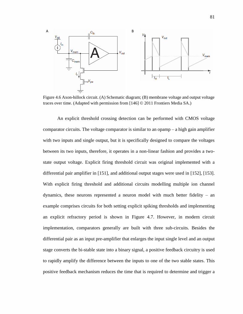
81
An explicit threshold crossing detection can be performed with CMOS voltage
comparator circuits. The voltage comparator is similar to an opamp – a high gain amplifier
with two inputs and single output, but it is specifically designed to compare the voltages
between its two inputs, therefore, it operates in a non-linear fashion and provides a two-
state output voltage. Explicit firing threshold circuit was original implemented with a
differential pair amplifier in [151], and additional output stages were used in [152], [153].
With explicit firing threshold and additional circuits modelling multiple ion channel
dynamics, these neurons represented a neuron model with much better fidelity – an
example comprises circuits for both setting explicit spiking thresholds and implementing
an explicit refractory period is shown in Figure 4.7. However, in modern circuit
implementation, comparators generally are built with three sub-circuits. Besides the
differential pair as an input pre-amplifier that enlarges the input single level and an output
stage converts the bi-stable state into a binary signal, a positive feedback circuitry is used
to rapidly amplify the difference between the inputs to one of the two stable states. This
positive feedback mechanism reduces the time that is required to determine and trigger a
A
B
Figure 4.6 Axon-hillock circuit. (A) Schematic diagram; (B) membrane voltage and output voltage
traces over time. (Adapted with permission from [146] © 2011 Frontiers Media SA.)
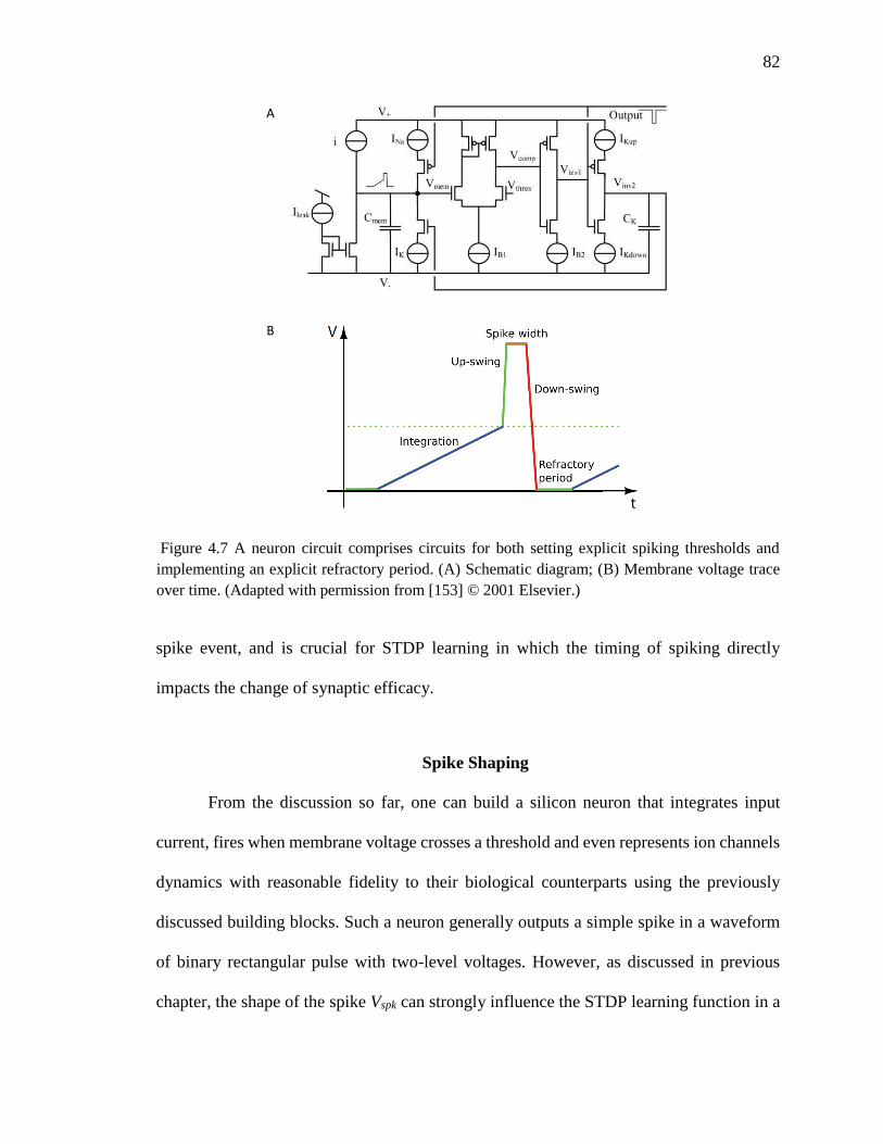
82
spike event, and is crucial for STDP learning in which the timing of spiking directly
impacts the change of synaptic efficacy.
Spike Shaping
From the discussion so far, one can build a silicon neuron that integrates input
current, fires when membrane voltage crosses a threshold and even represents ion channels
dynamics with reasonable fidelity to their biological counterparts using the previously
discussed building blocks. Such a neuron generally outputs a simple spike in a waveform
of binary rectangular pulse with two-level voltages. However, as discussed in previous
chapter, the shape of the spike Vspk can strongly influence the STDP learning function in a
A
B
Figure 4.7 A neuron circuit comprises circuits for both setting explicit spiking thresholds and
implementing an explicit refractory period. (A) Schematic diagram; (B) Membrane voltage trace
over time. (Adapted with permission from [153] © 2001 Elsevier.)
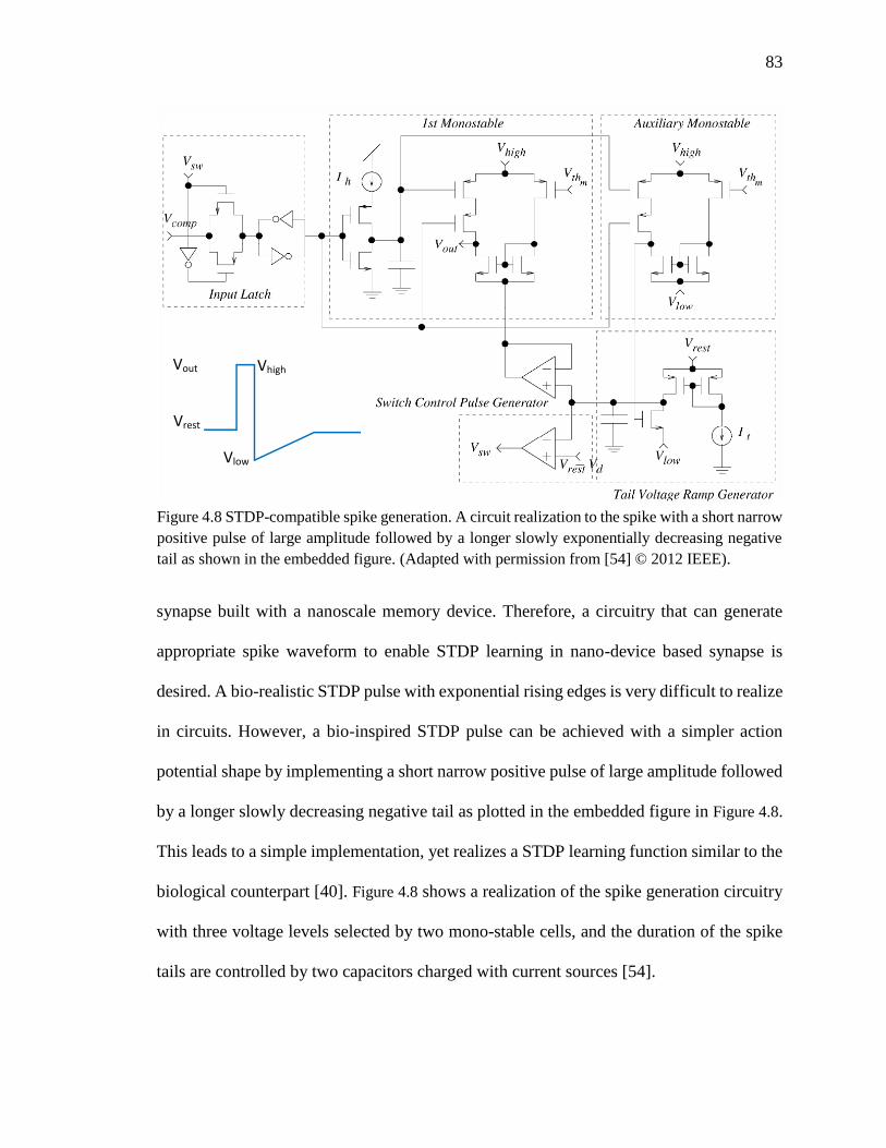
83
synapse built with a nanoscale memory device. Therefore, a circuitry that can generate
appropriate spike waveform to enable STDP learning in nano-device based synapse is
desired. A bio-realistic STDP pulse with exponential rising edges is very difficult to realize
in circuits. However, a bio-inspired STDP pulse can be achieved with a simpler action
potential shape by implementing a short narrow positive pulse of large amplitude followed
by a longer slowly decreasing negative tail as plotted in the embedded figure in Figure 4.8.
This leads to a simple implementation, yet realizes a STDP learning function similar to the
biological counterpart [40]. Figure 4.8 shows a realization of the spike generation circuitry
with three voltage levels selected by two mono-stable cells, and the duration of the spike
tails are controlled by two capacitors charged with current sources [54].
Vrest
Vhigh
Vlow
Vout
Figure 4.8 STDP-compatible spike generation. A circuit realization to the spike with a short narrow
positive pulse of large amplitude followed by a longer slowly exponentially decreasing negative
tail as shown in the embedded figure. (Adapted with permission from [54] © 2012 IEEE).
84
Spike-Frequency Adaptation and Adaptive Thresholds
When stimulated with constant current or continuous pulses, many neurons show a
reduction in the firing frequency of their spike response following an initial increase. This
phenomenon is called spike-frequency adaptation (SFA). SFA plays important role in the
neuron functionality and network behavior. In terms of computing aspect, SFA makes a
neuron shift from integrator to resonator, and then become more sensitive to synchronous
activity. In a group of neurons in local competition, SFA reduces the activity of the
dominating neuron for a short while, thus other neurons have opportunity to response to
the input simulation and overall leading to a better selectivity map in the group.
There are several biophysical mechanisms that can cause spike-frequency
adaptation. They all include a form of slow negative feedback to the excitability of the cell.
For the circuit realization of the SFA, one of the most direct way is to integrate the spikes
produced by the neuron itself and subtract the resulting current from the membrane
capacitance [149]. Figure 4.8 shows a silicon neuron design with this mechanism and its
firing rate measurements in response to a constant input current [154]. The other simple
method to model and realize SFA is to use adaptive thresholds. In this model, the neuron’s
spiking threshold voltage is changed with the neuron’s firing rate. For example, in a neuron
with opamp-based inverting integrator, each time the neuron fires, a small amount of
voltage should be added to the firing threshold to make it go upwards; on the other hand,
when there is no firing, the threshold voltage should decrease till the baseline level.
From the integrate-and-fire equation, these two ways to adapt spike frequency are
equivalent. An IFN fires when its membrane voltage meets the threshold
𝑉𝑚𝑒𝑚(𝑡) =1
𝐶𝑚𝑒𝑚∫ 𝐼(𝜏)𝑑𝜏
𝑡
𝑡0
+ 𝑉𝑚𝑒𝑚(𝑡0) > 𝑉𝑡ℎ𝑟.
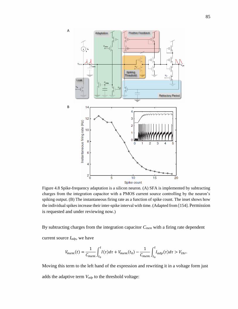
85
By subtracting charges from the integration capacitor Cmem with a firing rate dependent
current source Iadp, we have
𝑉𝑚𝑒𝑚(𝑡) =1
𝐶𝑚𝑒𝑚∫ 𝐼(𝜏)𝑑𝜏
𝑡
𝑡0
+ 𝑉𝑚𝑒𝑚(𝑡0) −1
𝐶𝑚𝑒𝑚∫ 𝐼𝑎𝑑𝑝(𝜏)𝑑𝜏
𝑡
𝑡0
> 𝑉𝑡ℎ𝑟.
Moving this term to the left hand of the expression and rewriting it in a voltage form just
adds the adaptive term Vadp to the threshold voltage:
A
B
Figure 4.8 Spike-frequency adaptation is a silicon neuron. (A) SFA is implemented by subtracting
charges from the integration capacitor with a PMOS current source controlling by the neuron’s
spiking output. (B) The instantaneous firing rate as a function of spike count. The inset shows how
the individual spikes increase their inter-spike interval with time. (Adapted from [154]. Permission
is requested and under reviewing now.)
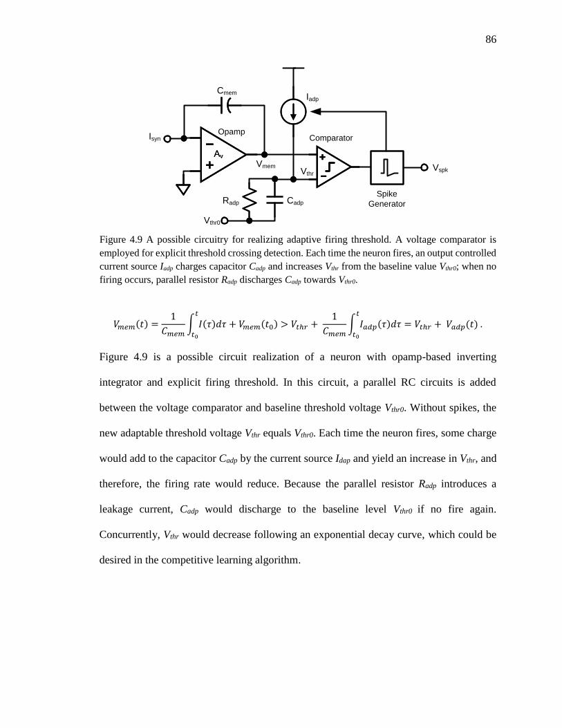
86
𝑉𝑚𝑒𝑚(𝑡) =1
𝐶𝑚𝑒𝑚∫ 𝐼(𝜏)𝑑𝜏
𝑡
𝑡0
+ 𝑉𝑚𝑒𝑚(𝑡0) > 𝑉𝑡ℎ𝑟 + 1
𝐶𝑚𝑒𝑚∫ 𝐼𝑎𝑑𝑝(𝜏)𝑑𝜏
𝑡
𝑡0
= 𝑉𝑡ℎ𝑟 + 𝑉𝑎𝑑𝑝(𝑡) .
Figure 4.9 is a possible circuit realization of a neuron with opamp-based inverting
integrator and explicit firing threshold. In this circuit, a parallel RC circuits is added
between the voltage comparator and baseline threshold voltage Vthr0. Without spikes, the
new adaptable threshold voltage Vthr equals Vthr0. Each time the neuron fires, some charge
would add to the capacitor Cadp by the current source Idap and yield an increase in Vthr, and
therefore, the firing rate would reduce. Because the parallel resistor Radp introduces a
leakage current, Cadp would discharge to the baseline level Vthr0 if no fire again.
Concurrently, Vthr would decrease following an exponential decay curve, which could be
desired in the competitive learning algorithm.
Cmem
Isyn
Vmem
AvAv
Comparator
Spike
Generator
Vspk
Vthr0
Iadp
CadpRadp
Opamp
Vthr
Figure 4.9 A possible circuitry for realizing adaptive firing threshold. A voltage comparator is
employed for explicit threshold crossing detection. Each time the neuron fires, an output controlled
current source Iadp charges capacitor Cadp and increases Vthr from the baseline value Vthr0; when no
firing occurs, parallel resistor Radp discharges Cadp towards Vthr0.

87
Axons and Dendritic Trees
Axon and dendritic tree are other another building blocks for silicon neurons. Axon
propagates efferent impulsive signals from the soma to distant neurons in other portion of
the network that far away from the current neuron. This structure is crucial especially for
large-scale neural network. Axon circuitry is basically a series of signal repeaters to keep
the signal integrity of spikes. Dendritic tree could act as independent computational units
as suggested by neuroscience experiments. Because the individually separated dendritic
branches can produce different post-synaptic current with different time delays, the
dendritic tree of a single neuron can act as a multilayer computational network that allows
parallel processing of the inputs from pre-synaptic neurons before they are combined in the
soma. More information about axon and dendritic circuitry can be found in [155] and
[149].
Summary
In this chapter, the major building blocks to build analog spiking neurons were
introduced together with several neuron design styles and examples. Because the easy and
compact mapping from neuron model to analog circuits, LIF neuron is the most popular
model for the implementation of neuromorphic systems. Thus, the integrator and threshold
firing are the most important building blocks of a LIF neuron. With appropriate design and
assembly of these building blocks, it is possible to use silicon integrate and fire neurons to
mimic neuron behaviors and dynamics with reasonable faithfulness, and then is very useful
for real-time emulation of a biological neural network. However, with the primary
objective of this research is computation, faithfully representing the neuron dynamics may
not be necessary and wasteful in terms of power consumption and silicon area. Thus

88
compact designs with appropriate abstraction of the neuron model are employed.
Furthermore, it is worth to point out that the spike waveform shapes are generally neglected
in some neuromorphic systems, which were designed for biological neural network
emulation, but are critical to synaptic plasticity and the meaningful interface with RRAM
devices as synapses. Therefore, they are considered as an essential building block for our
neuron designs and implementation that follow in the next chapter.
89
CHAPTER 5
A CMOS SPIKING NEURON FOR DENSE RESISTIVE SYNAPSES
AND IN SITU STDP LEARNING
In previous chapter, several silicon neuron design styles have been reviewed along
with other circuit building blocks. These designs model certain aspects of the biological
neurons, however, most of them focus on faithful modeling of the ionic channel dynamics
in biological spiking neurons, and require the synapses to act as controlled current sources
[146], [156], [157]. As a result, they consume large silicon area, and therefore are not
amenable for large-scale neuromorphic networks with a massive number of silicon
neurons. The emergence of nanoscale RRAM synapses has triggered a growing interest in
integrating these devices with silicon neurons to realize novel brain and nanotechnology
inspired neuromorphic systems [43]–[52]. In these systems, researchers have used bio-
inspired LIF neuron models as an alternative to the complex bio-mimetic neuron models
to implement large networks of interconnected spiking neurons. The IFN model captures
the essential transient spiking behavior of the neuron with reasonable accuracy for use in
learning while requiring a relative low number of transistors for its implementation.
Currently, the IFNs used in neuromorphic systems [47], [156], [158], [159] need either
extra training circuitry attached to resistive synapses, thus eliminating most of the density
advantages gained by using RRAM synapses; or employ different waveforms for pre- and

90
post-synaptic spikes, thus introducing undesirable circuit overhead which limits power and
area budget of a large-scale neuromorphic system. This chapter presents a novel leaky
integrate-and-fire neuron design and the respective chip implementation. The proposed
neuron works in a dual-mode operation with a single opamp and enables online learning
directly with dense two-terminal resistive synapses. Several simulations and final chip
measurements shows neuron’s ability to drive dense resistive synapses, and realize in situ
associative learning.
Accommodating RRAM Synapses
Nano RRAM devices are non-volatile memory devices that do not consume power
to retain their state. They are simple in structure (typically two-terminal), nanoscale in
dimension, consuming very little energy to change their conductance and are compatible
with CMOS process technology. Because the RRAM devices generally have two voltage-
type thresholds for conductance change, they are able to emulate STDP behavior similar
to biological synapses with pair-wise spikes. As a result, nanoscale RRAM devices are
very promising for implementing dense electronic synapses, and for synergistically
interfacing with CMOS neurons in large-scale brain-inspired computing systems. With this
context, nanoscale RRAM device is expected to be used as the synapse in its minimal form
in a crossbar array, i.e. without any other associated device or circuits. Also, the
conductance change depends on the over-threshold potential produced by the pre- and post-
synaptic spikes applied across it, while keeping its conductance unchanged when an under-
threshold potential spike is applied across it.
91
Existing IFN circuits fail to fit into a real large-scale neuromorphic system with
resistive synapses due to three major challenges: (1) in-situ learning in resistive synapses,
(2) driving capability and (3) accessory circuits attached to the synapses.
Firstly, conventional IFN circuits are designed to generate spikes to match the
spiking behavior of certain biological neurons [146], and then, synaptic learning is barely
taken into consideration together with the neuron circuit. In Chapter 3, it has been shown
that recent nanoscale RRAMs have demonstrated biological plausible STDP learning
which requires the neurons to produce spikes with specific shapes. Thus, to realize online
learning that leverages the dense-integration with nanoscale emerging devices, a pulse
generator is needed to produce spikes which are compatible with the electrical properties
of the two-terminal resistive synapse. Moreover, a STDP-compatible spike shape with
digitally configurable pulse amplitudes and widths is desired to enable the designed silicon
neuron to interface with synapse devices with different properties (e.g. programing
thresholds and operating frequency) and incorporate spike-based learning algorithms, both
of which are continuously evolving.
Secondly, in order to integrate currents across several resistive synapses (with
1MΩ-1GΩ resistance range) and drive thousands of these in parallel, the conventional
current-input IFN architecture [3] cannot be directly employed; current summing
overheads and the large current drive required from the neurons would be prohibitive.
Instead, an opamp-based IFN is desirable as it provides the required current summing node
as well as a large current drive capability.
Finally, the primary benefit of using nanoscale resistive memory as a synapse is its
high integration capability that is ideal for resolving the synaptic density challenge in
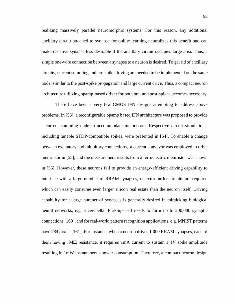
92
realizing massively parallel neuromorphic systems. For this reason, any additional
ancillary circuit attached to synapse for online learning neutralizes this benefit and can
make resistive synapse less desirable if the ancillary circuit occupies large area. Thus, a
simple one-wire connection between a synapse to a neuron is desired. To get rid of ancillary
circuits, current summing and pre-spike driving are needed to be implemented on the same
node; similar to the post-spike propagation and large current drive. Thus, a compact neuron
architecture utilizing opamp-based driver for both pre- and post-spikes becomes necessary.
There have been a very few CMOS IFN designs attempting to address above
problems. In [53], a reconfigurable opamp based IFN architecture was proposed to provide
a current summing node to accommodate memristors. Respective circuit simulations,
including tunable STDP-compatible spikes, were presented in [54]. To enable a change
between excitatory and inhibitory connections, a current conveyor was employed to drive
memristor in [55], and the measurement results from a ferroelectric memristor was shown
in [56]. However, these neurons fail to provide an energy-efficient driving capability to
interface with a large number of RRAM synapses, or extra buffer circuits are required
which can easily consume even larger silicon real estate than the neuron itself. Driving
capability for a large number of synapses is generally desired in mimicking biological
neural networks, e.g. a cerebellar Purkinje cell needs to form up to 200,000 synaptic
connections [160], and for real-world pattern recognition applications, e.g. MNIST patterns
have 784 pixels [161]. For instance, when a neuron drives 1,000 RRAM synapses, each of
them having 1MΩ resistance, it requires 1mA current to sustain a 1V spike amplitude
resulting in 1mW instantaneous power consumption. Therefore, a compact neuron design
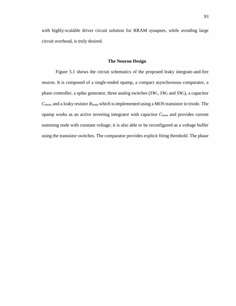
93
with highly-scalable driver circuit solution for RRAM synapses, while avoiding large
circuit overhead, is truly desired.
The Neuron Design
Figure 5.1 shows the circuit schematics of the proposed leaky integrate-and-fire
neuron. It is composed of a single-ended opamp, a compact asynchronous comparator, a
phase controller, a spike generator, three analog switches (SW1, SW2 and SW3), a capacitor
Cmem, and a leaky resistor Rleaky which is implemented using a MOS transistor in triode. The
opamp works as an active inverting integrator with capacitor Cmem and provides current
summing node with constant voltage; it is also able to be reconfigured as a voltage buffer
using the transistor switches. The comparator provides explicit firing threshold. The phase
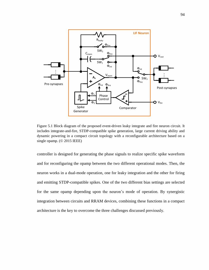
94
controller is designed for generating the phase signals to realize specific spike waveform
and for reconfiguring the opamp between the two different operational modes. Then, the
neuron works in a dual-mode operation, one for leaky integration and the other for firing
and emitting STDP-compatible spikes. One of the two different bias settings are selected
for the same opamp depending upon the neuron’s mode of operation. By synergistic
integration between circuits and RRAM devices, combining these functions in a compact
architecture is the key to overcome the three challenges discussed previously.
LIF Neuron
Post-synapses
Cmem
Vthr
Pre-synapses
Phase Control
Фint Фfire
Vmem
Vrest
Rleaky
Ф1
Ф2
SW1
SW2
AvAv SW3
Фint
Фfire
Фfire
Фint
Фfire
ComparatorSpike Generator
Figure 5.1 Block diagram of the proposed event-driven leaky integrate and fire neuron circuit. It
includes integrate-and-fire, STDP-compatible spike generation, large current driving ability and
dynamic powering in a compact circuit topology with a reconfigurable architecture based on a
single opamp. (© 2015 IEEE)

95
Reconfigurable Architecture and Dual-Mode Operation
Dual-mode operation is realized by using a single-ended opamp that is reconfigured
both an integrator, as well as a buffered driver for resistive load during the firing events.
Here, a power-optimized opamp operates in two asynchronous modes: integration and
firing modes, as illustrated in Figure 5.2.
The integration mode
As shown in Figure 5.2.A, in this mode, the phase control signal Φint is set to active,
and switch SW1 is set to connect “membrane” capacitor Cmem with the opamp output. With
Φfire working as a complementary signal to Φint, switches SW2 and SW3 are both open.
Thanks to the spike generator that is designed to hold a voltage equal to the rest potential
Vrest during the non-firing time, the positive input of opamp is set to voltage Vrest, which
consequently acts as the common-mode voltage. With this configuration, the opamp
realizes a leaky integrator with the leak-rate controlled by Rleaky, and charges Cmem resulting
in a change in the neuron “membrane potential” Vmem. Next, the neuron sums the currents
injected into it, and causes the output voltage to move down. Then, the potential Vmem is
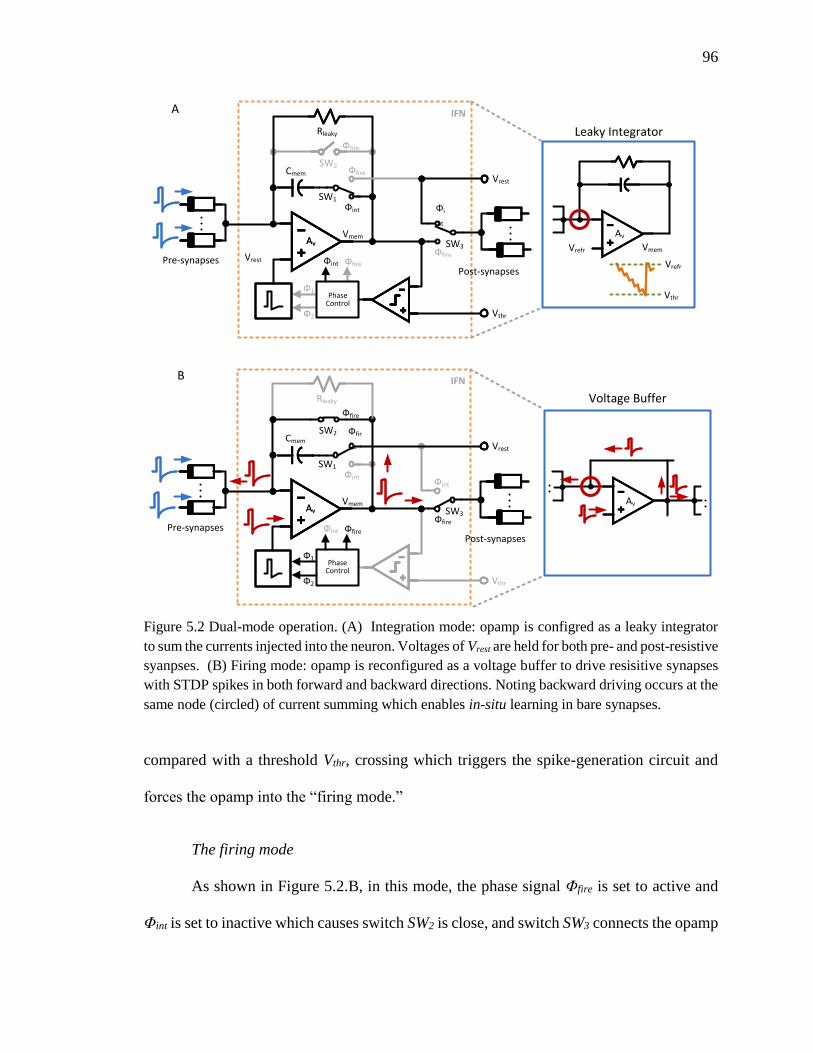
96
compared with a threshold Vthr, crossing which triggers the spike-generation circuit and
forces the opamp into the “firing mode.”
The firing mode
As shown in Figure 5.2.B, in this mode, the phase signal Φfire is set to active and
Φint is set to inactive which causes switch SW2 is close, and switch SW3 connects the opamp
IFN
IFN
Post-synapses
Cmem
Vthr
Pre-synapses Фint Фfire
Vmem
Vrest
Rleaky
Ф1
Ф2
SW1
SW2
AvAv SW3
Фint
Фfire
Фfire
Фi
nt
Фfire
Post-synapses
Cmem
Vthr
Pre-synapses Фint Фfire
Vmem
Vrest
Rleaky
Ф1
Ф2
SW1
SW2
AvAv SW3
Фint
Фfir
e
Фfire
Фint
Фfire
Av
Av
Vrefr Vmem
Vrefr
VthrPhase Control
Vrest
Phase Control
Leaky Integrator
Voltage Buffer
A
B
Figure 5.2 Dual-mode operation. (A) Integration mode: opamp is configred as a leaky integrator
to sum the currents injected into the neuron. Voltages of Vrest are held for both pre- and post-resistive
syanpses. (B) Firing mode: opamp is reconfigured as a voltage buffer to drive resisitive synapses
with STDP spikes in both forward and backward directions. Noting backward driving occurs at the
same node (circled) of current summing which enables in-situ learning in bare synapses.

97
output to the p ost-synapses. Consequently, the opamp is reconfigured as a voltage
follower/buffer. STDP spike generator creates the required action potential waveform Vspk
and passes it to input port of the buffer, which is positive input of the opamp. Noting both
pre-synapses and post-synapses are shorted to the buffer output, the neuron propagates
post-synaptic spikes in the direction of the input synapses on the same port where currents
were being summed. At the same time, the neuron also propagates the pre-synaptic spikes
in the forward direction on the same node where the post-synapses are driven. Furthermore,
SW1 is connected to Vrest, which then discharges and resets the voltage on the membrane
capacitor Cmem.
Opamp and Dynamic Biasing
The energy-efficiency of the neuron is tied to the above discussed dual-mode
operation. For dynamic biasing/powering, the opamp is designed with the output stage
being split into a major branch and a minor branch. The major branch provides large current
driving capability; while the minor low-power branch works with the first stage to provide
the desired gain in the integration mode. Two complementary signals Φint and Φfire are used
to bias the opamp in low-power configuration by disabling the major branch during
integration and discharging modes, while enabling it to drive large currents in the firing
mode.
In this work, a compact design [162] is modified with an embedded split driver to
realize a dynamically powered opamp, as shown in Figure 5.3. A two-stage opamp is
suitable to obtain a compact design while at the same time achieving sufficiently large gain.
The opamp contains a folded cascode input stage and a class-AB output stage. By
incorporating the class-AB driver circuit in the folded-cascode summing circuit of the input
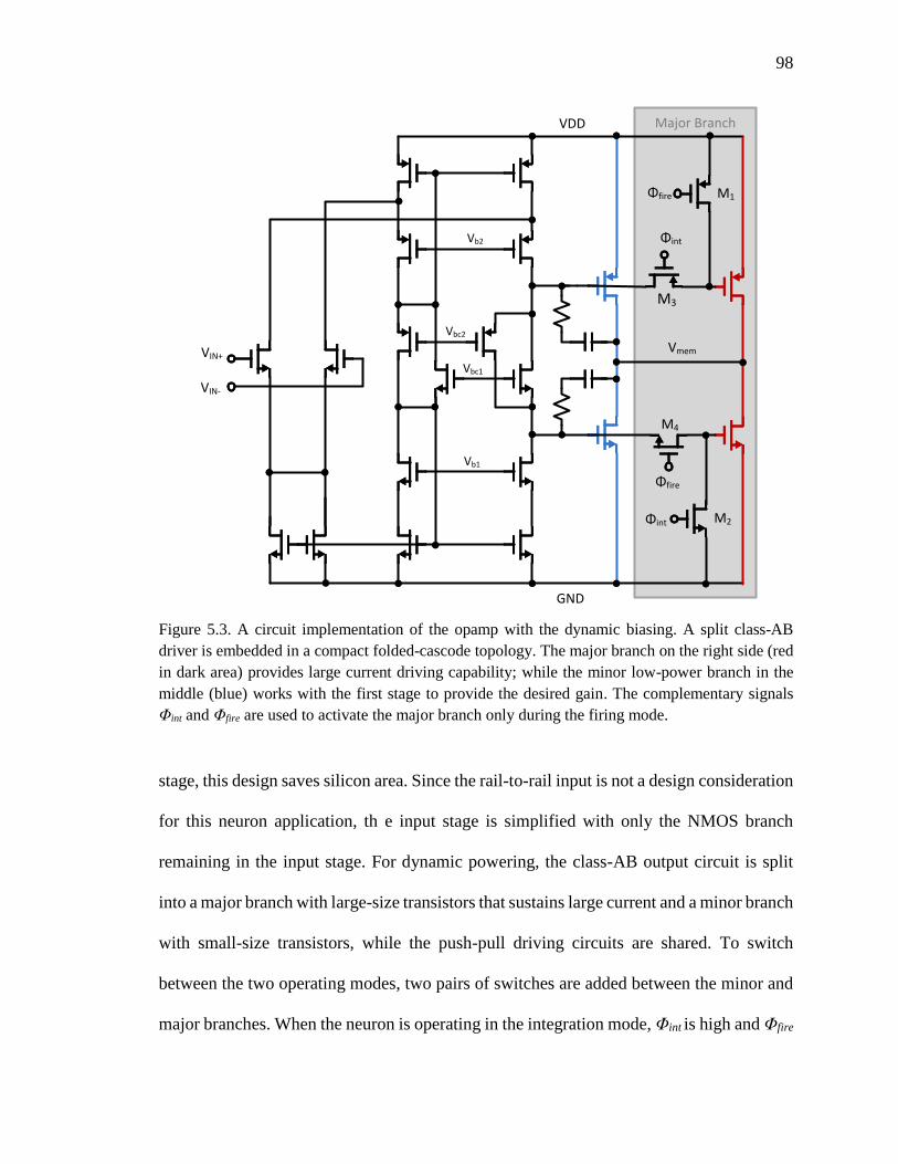
98
stage, this design saves silicon area. Since the rail-to-rail input is not a design consideration
for this neuron application, th e input stage is simplified with only the NMOS branch
remaining in the input stage. For dynamic powering, the class-AB output circuit is split
into a major branch with large-size transistors that sustains large current and a minor branch
with small-size transistors, while the push-pull driving circuits are shared. To switch
between the two operating modes, two pairs of switches are added between the minor and
major branches. When the neuron is operating in the integration mode, Φint is high and Φfire
Major Branch
VIN+
VIN-
VDD
GND
Vmem
Vb1
Vb2
Vbc1
Vbc2
Φint
Φfire
Φfire
Φint
M1
M2
M3
M4
Figure 5.3. A circuit implementation of the opamp with the dynamic biasing. A split class-AB
driver is embedded in a compact folded-cascode topology. The major branch on the right side (red
in dark area) provides large current driving capability; while the minor low-power branch in the
middle (blue) works with the first stage to provide the desired gain. The complementary signals
Φint and Φfire are used to activate the major branch only during the firing mode.

99
is low. Then, transistor M1 is on to pull-up the PMOS in major transistor to VDD and turn it
off; in a similar way, M2 is on to pull-down the NMOS to ground and turn it off. At the
same time, the two transistors, M3 and M4 between the minor branch and major branch are
turned off to isolate the major branch from the opamp’s output. For stable operation, the
compensation capacitors and zero nulling resistors need to be calculated and simulated for
both of the two operational modes. Since the second pole of this opamp is proportionally
related to the trans-conductance of the second stage, once the opamp is compensated for
the lower-power mode (i.e. the integration mode), a larger second-stage trans-conductance
due to the operation of the major branch brings in additional capacitance and causes the
two dominant poles to further separate from each other (i.e. additional pole splitting is
achieved). Consequently, the whole system is automatically compensated and stabilized
when operating in the firing mode.
Asynchronous Comparator
Figure 5.4 shows the comparator used in this neuron design. It comprises of two
cascaded differential amplifiers. The inner amplifier is a gain stage based on source-
coupled differential pair with diode-connec ted load devices. The output of the differential
pair is further enhanced and regenerated upon using the cross-coupled latch that provides
positive feedback. The outer amplifier further enhances the overall gain and converts the
intermediate comparison result into a full-scale binary output voltage [163].
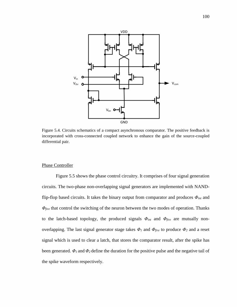
100
Phase Controller
Figure 5.5 shows the phase control circuitry. It comprises of four signal generation
circuits. The two-phase non-overlapping signal generators are implemented with NAND-
flip-flop based circuits. It takes the binary output from comparator and produces Φint and
Φfire that control the switching of the neuron between the two modes of operation. Thanks
to the latch-based topology, the produced signals Φint and Φfire are mutually non-
overlapping. The last signal generator stage takes Φ1 and Φfire to produce Φ2 and a reset
signal which is used to clear a latch, that stores the comparator result, after the spike has
been generated. Φ1 and Φ2 define the duration for the positive pulse and the negative tail of
the spike waveform respectively.
VDD
GND
Vthr
Vbn
Vcom
Vin
Figure 5.4. Circuits schematics of a compact asynchronous comparator. The positive feedback is
incorporated with cross-connected coupled network to enhance the gain of the source-coupled
differential pair.
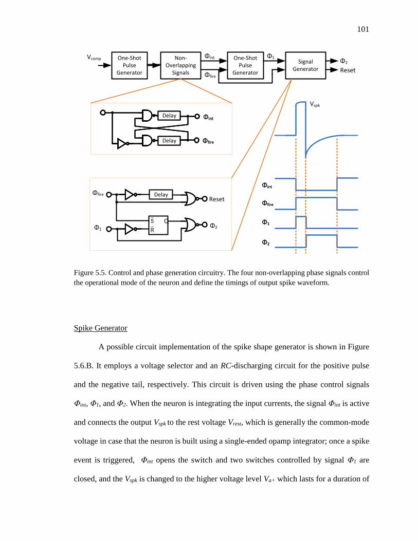
101
Spike Generator
A possible circuit implementation of the spike shape generator is shown in Figure
5.6.B. It employs a voltage selector and an RC-discharging circuit for the positive pulse
and the negative tail, respectively. This circuit is driven using the phase control signals
Φint, Φ1, and Φ2. When the neuron is integrating the input currents, the signal Φint is active
and connects the output Vspk to the rest voltage Vrest, which is generally the common-mode
voltage in case that the neuron is built using a single-ended opamp integrator; once a spike
event is triggered, Φint opens the switch and two switches controlled by signal Φ1 are
closed, and the Vspk is changed to the higher voltage level Va+ which lasts for a duration of
One-Shot Pulse
Generator
Non-Overlapping
Signals
One-Shot Pulse
Generator
SignalGenerator
Φint
Φfire
Φ1Φ2
Vcomp
Reset
Φ1
Φ2
Φint
Φfire
Φ1
Φ2
Φint
Φfire
DelayΦfire
Φ1Φ2
Reset
Q
Delay
Delay
Φint
Φfire
Delay
Delay
Φint
Φfire
Vspk
S
R
Figure 5.5. Control and phase generation circuitry. The four non-overlapping phase signals control
the operational mode of the neuron and define the timings of output spike waveform.
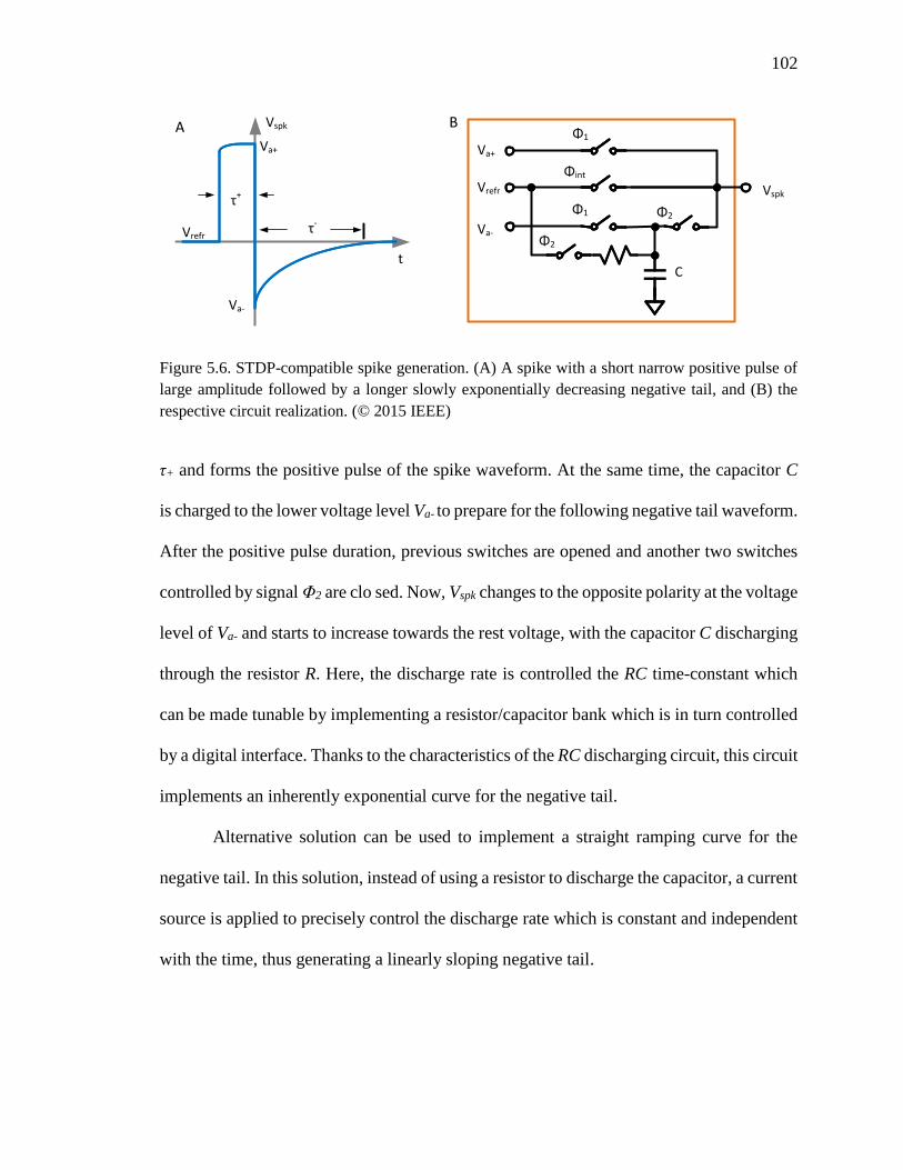
102
τ+ and forms the positive pulse of the spike waveform. At the same time, the capacitor C
is charged to the lower voltage level Va- to prepare for the following negative tail waveform.
After the positive pulse duration, previous switches are opened and another two switches
controlled by signal Φ2 are clo sed. Now, Vspk changes to the opposite polarity at the voltage
level of Va- and starts to increase towards the rest voltage, with the capacitor C discharging
through the resistor R. Here, the discharge rate is controlled the RC time-constant which
can be made tunable by implementing a resistor/capacitor bank which is in turn controlled
by a digital interface. Thanks to the characteristics of the RC discharging circuit, this circuit
implements an inherently exponential curve for the negative tail.
Alternative solution can be used to implement a straight ramping curve for the
negative tail. In this solution, instead of using a resistor to discharge the capacitor, a current
source is applied to precisely control the discharge rate which is constant and independent
with the time, thus generating a linearly sloping negative tail.
VspkVrefr
Va+
Va-
Φ1
Φ2Φ1
Φ2
Φint
Vrefr
Va+
Va-
Vspk
t
τ+
τ-
A B
C
Figure 5.6. STDP-compatible spike generation. (A) A spike with a short narrow positive pulse of
large amplitude followed by a longer slowly exponentially decreasing negative tail, and (B) the
respective circuit realization. (© 2015 IEEE)

103
Circuit Simulations
The circuits were designed in Cadence analog design environment and the
simulations were carried out with the Spectre circuit simulator. The silicon neuron was
realized with an IBM 180nm CMOS process.
Opamp Characterizations
A two-stage opamp was used with folded-cascode topology for the first stage
followed by a dynamically biased class-AB output stage, as discussed earlier. With 1.8 V
power supply, 900 mV common voltage, an equivalent load of 1 kΩ in parallel with 20 pF,
the opamp has 39 dB DC gain, 3 V/µs slew rate and 5 MHz unity-gain frequency in
integration mode; and 60 dB DC gain, 15 MHz unit gain frequency and 15 V/µs slew rate
in firing mode.
Integration, Firing and Leaking
A test circuitry that consists of a neuron and three input resistor synapses was used
to evaluate the spatiotemporal integration, firing with threshold, spiking and leaky
functionalities, as shown in Figure 5.7. In this setup, a 2 pF integration capacitor Cmem was
used, firing threshold was set to 200 mV, and a standard spike shape as shown in Figure
5.6.A was employed with the Va+ = 350 mV, Va- = 150 mV, τ+ = 0.5 µs and τ- = 2.5 µs.
To verify the spatiotemporal integration, three spike trains with 900 mV rest
voltage, 100mV positive amplitude, 100 ns pulse with 1 µs interleaving were sent to the
input branches. All the three resistor synapses have the same strength equal to 100 kΩ.
Under this configuration, an input spike runs through the resistor produces a 1 µA current
flowing into the neuron. Figure 5.8 shows the response of membrane voltage Vmem and the
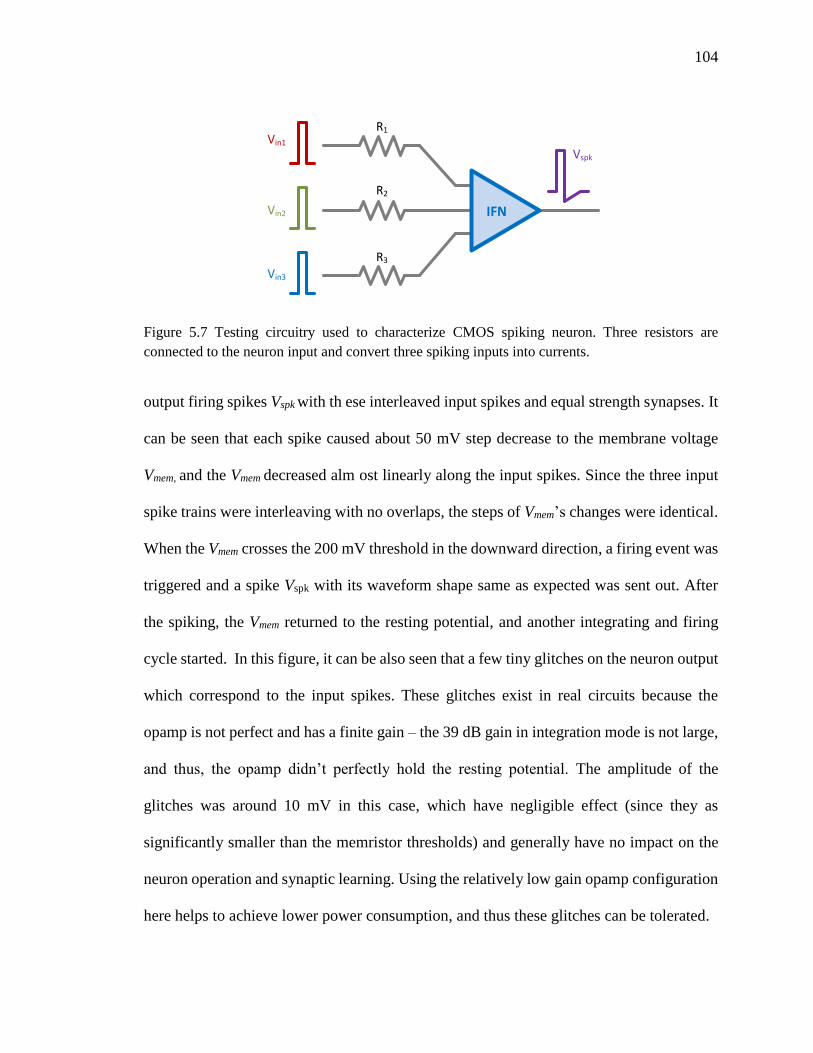
104
output firing spikes Vspk with th ese interleaved input spikes and equal strength synapses. It
can be seen that each spike caused about 50 mV step decrease to the membrane voltage
Vmem, and the Vmem decreased alm ost linearly along the input spikes. Since the three input
spike trains were interleaving with no overlaps, the steps of Vmem’s changes were identical.
When the Vmem crosses the 200 mV threshold in the downward direction, a firing event was
triggered and a spike Vspk with its waveform shape same as expected was sent out. After
the spiking, the Vmem returned to the resting potential, and another integrating and firing
cycle started. In this figure, it can be also seen that a few tiny glitches on the neuron output
which correspond to the input spikes. These glitches exist in real circuits because the
opamp is not perfect and has a finite gain – the 39 dB gain in integration mode is not large,
and thus, the opamp didn’t perfectly hold the resting potential. The amplitude of the
glitches was around 10 mV in this case, which have negligible effect (since they as
significantly smaller than the memristor thresholds) and generally have no impact on the
neuron operation and synaptic learning. Using the relatively low gain opamp configuration
here helps to achieve lower power consumption, and thus these glitches can be tolerated.
Figure 5.7 Testing circuitry used to characterize CMOS spiking neuron. Three resistors are
connected to the neuron input and convert three spiking inputs into currents.
R1
R2
R3
IFN
Vin1
Vin2
Vin3
Vspk
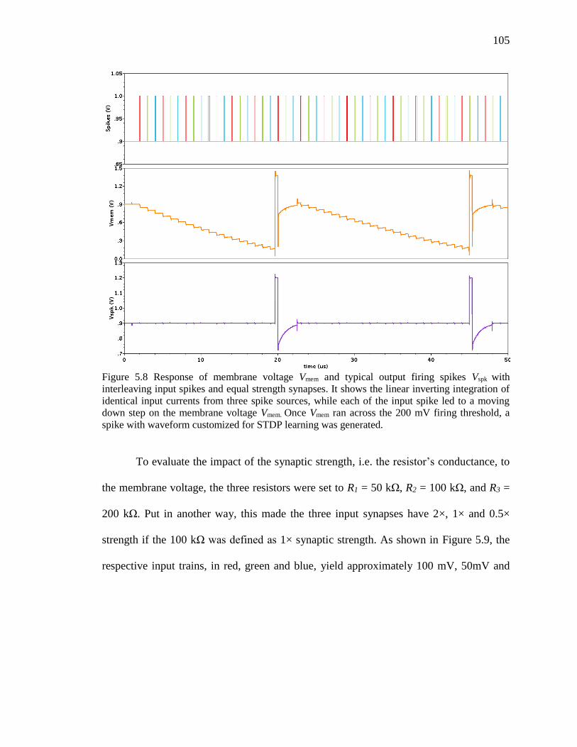
105
To evaluate the impact of the synaptic strength, i.e. the resistor’s conductance, to
the membrane voltage, the three resistors were set to R1 = 50 kΩ, R2 = 100 kΩ, and R3 =
200 kΩ. Put in another way, this made the three input synapses have 2×, 1× and 0.5×
strength if the 100 kΩ was defined as 1× synaptic strength. As shown in Figure 5.9, the
respective input trains, in red, green and blue, yield approximately 100 mV, 50mV and
Figure 5.8 Response of membrane voltage Vmem and typical output firing spikes Vspk with
interleaving input spikes and equal strength synapses. It shows the linear inverting integration of
identical input currents from three spike sources, while each of the input spike led to a moving
down step on the membrane voltage Vmem. Once Vmem ran across the 200 mV firing threshold, a
spike with waveform customized for STDP learning was generated.
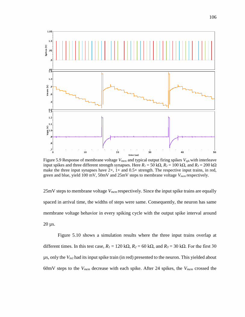
106
25mV steps to membrane voltage Vmem respectively. Since the input spike trains are equally
spaced in arrival time, the widths of steps were same. Consequently, the neuron has same
membrane voltage behavior in every spiking cycle with the output spike interval around
20 µs.
Figure 5.10 shows a simulation results where the three input trains overlap at
different times. In this test case, R1 = 120 kΩ, R2 = 60 kΩ, and R3 = 30 kΩ. For the first 30
µs, only the Vin1 had its input spike train (in red) presented to the neuron. This yielded about
60mV steps to the Vmem decrease with each spike. After 24 spikes, the Vmem crossed the
Figure 5.9 Response of membrane voltage Vmem and typical output firing spikes Vspk with interleave
input spikes and three different strength synapses. Here R1 = 50 kΩ, R2 = 100 kΩ, and R3 = 200 kΩ
make the three input synapses have 2×, 1× and 0.5× strength. The respective input trains, in red,
green and blue, yield 100 mV, 50mV and 25mV steps to membrane voltage Vmem respectively.
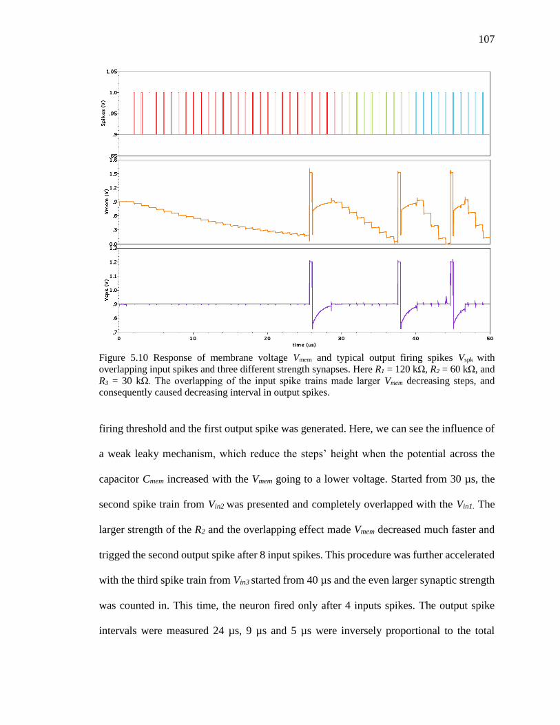
107
firing threshold and the first output spike was generated. Here, we can see the influence of
a weak leaky mechanism, which reduce the steps’ height when the potential across the
capacitor Cmem increased with the Vmem going to a lower voltage. Started from 30 µs, the
second spike train from Vin2 was presented and completely overlapped with the Vin1. The
larger strength of the R2 and the overlapping effect made Vmem decreased much faster and
trigged the second output spike after 8 input spikes. This procedure was further accelerated
with the third spike train from Vin3 started from 40 µs and the even larger synaptic strength
was counted in. This time, the neuron fired only after 4 inputs spikes. The output spike
intervals were measured 24 µs, 9 µs and 5 µs were inversely proportional to the total
Figure 5.10 Response of membrane voltage Vmem and typical output firing spikes Vspk with
overlapping input spikes and three different strength synapses. Here R1 = 120 kΩ, R2 = 60 kΩ, and
R3 = 30 kΩ. The overlapping of the input spike trains made larger Vmem decreasing steps, and
consequently caused decreasing interval in output spikes.
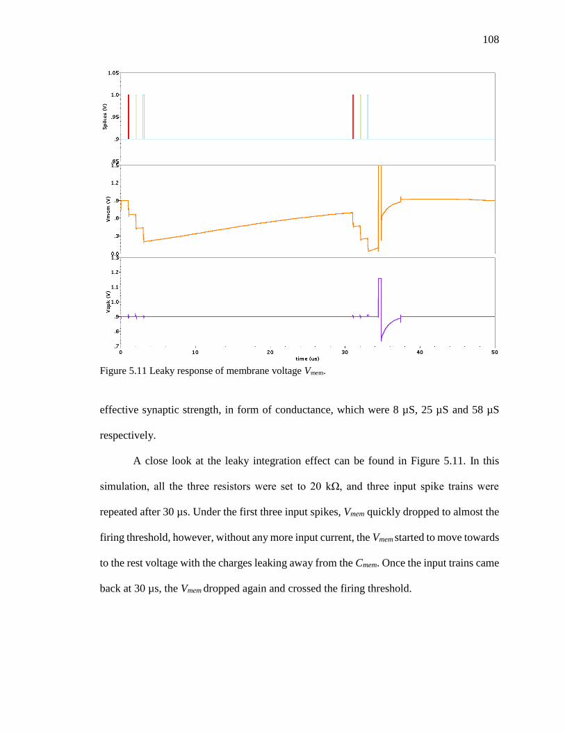
108
effective synaptic strength, in form of conductance, which were 8 µS, 25 µS and 58 µS
respectively.
A close look at the leaky integration effect can be found in Figure 5.11. In this
simulation, all the three resistors were set to 20 kΩ, and three input spike trains were
repeated after 30 µs. Under the first three input spikes, Vmem quickly dropped to almost the
firing threshold, however, without any more input current, the Vmem started to move towards
to the rest voltage with the charges leaking away from the Cmem. Once the input trains came
back at 30 µs, the Vmem dropped again and crossed the firing threshold.
Figure 5.11 Leaky response of membrane voltage Vmem.
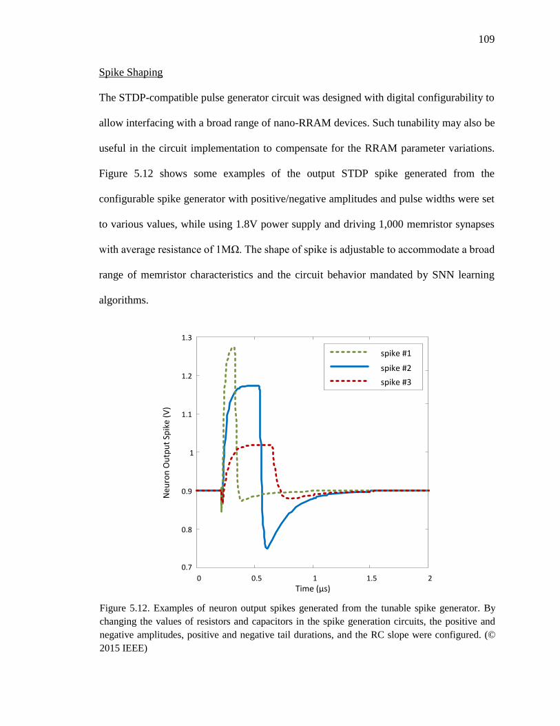
109
Spike Shaping
The STDP-compatible pulse generator circuit was designed with digital configurability to
allow interfacing with a broad range of nano-RRAM devices. Such tunability may also be
useful in the circuit implementation to compensate for the RRAM parameter variations.
Figure 5.12 shows some examples of the output STDP spike generated from the
configurable spike generator with positive/negative amplitudes and pulse widths were set
to various values, while using 1.8V power supply and driving 1,000 memristor synapses
with average resistance of 1MΩ. The shape of spike is adjustable to accommodate a broad
range of memristor characteristics and the circuit behavior mandated by SNN learning
algorithms.
0 0.5 1 1.5 2
0.7
0.8
0.9
1
1.1
1.2
1.3
Neu
ron
Ou
tpu
t Sp
ike
(V)
Time (µs)
spike #1
spike #2
spike #3
Figure 5.12. Examples of neuron output spikes generated from the tunable spike generator. By
changing the values of resistors and capacitors in the spike generation circuits, the positive and
negative amplitudes, positive and negative tail durations, and the RC slope were configured. (©
2015 IEEE)

110
Power Consumption
To evaluate energy-efficiency, the neurons were designed to have the capability to
drive up to 10,000 resistive synapses with an assumption that the distribution of resistive
states is tightly arranged around 1 MΩ resistance. This yields a 100 Ω equivalent resistive
load. Figure 5.13 shows the neuron consumed 13 μA baseline current in the integration
mode. When firing, the dynamically biased output stage consumed around 56 μA current
in the class-AB stage, and drove the remaining current to memristor synapses: a 1.4 mA
peak current for 10,000 memristor synapses sustained a spike voltage amplitude of 140
mV. The current sunk by the synapses follows Ohm’s law (linear region of the hysteresis
loop) due to its resistive nature. Insufficient current supplied to the resistive synapses will
cause a lower spike voltage amplitude that may fail STDP learning. Here, the widely used
energy-efficiency figure-of-merit for silicon neuron, pJ / spike / synapse, becomes
dependent on the resistance of synapses, and therefore, is not an appropriate descriptor of
neuron’s efficiency. Instead, the power efficiency η during the maximum driving condition
(at equivalent resistive load) should be used, i.e.
𝜂 =𝐼mr
𝐼mr + 𝐼IFN,
where Imr is the current consumed by a resistive synapse and IIFN is the current consumed
by a silicon neuron. Our simulation demonstrated η = 97% with 100 Ω for the selected
memristor, and a baseline power consumption of 22 μW with a 1.8 V power supply voltage.
This baseline power consumption doesn’t change with the neuron’s driving capability
thanks to the dual-mode operation. As a comparison, a neuron without dynamic biasing
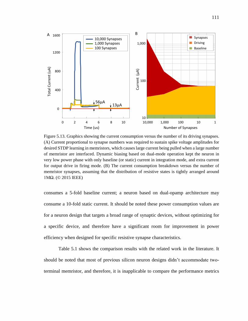
111
consumes a 5-fold baseline current; a neuron based on dual-opamp architecture may
consume a 10-fold static current. It should be noted these power consumption values are
for a neuron design that targets a broad range of synaptic devices, without optimizing for
a specific device, and therefore have a significant room for improvement in power
efficiency when designed for specific resistive synapse characteristics.
Table 5.1 shows the comparison results with the related work in the literature. It
should be noted that most of previous silicon neuron designs didn’t accommodate two-
terminal memristor, and therefore, it is inapplicable to compare the performance metrics
0 2 4 6 8 10
0
400
800
1200
1600
Time (us)
Tota
l Cu
rren
t (u
A)
13µA56µA
1,000 Synapses100 Synapses
10,000 SynapsesA
10
100
1,000
10,000 1,000 100 10 1
Cu
rren
t (
µA
)
Number of Synapses
Synapses
Driving
Baseline
B
Figure 5.13. Graphics showing the current consumption versus the number of its driving synapses.
(A) Current proportional to synapse numbers was required to sustain spike voltage amplitudes for
desired STDP learning in memristors, which causes large current being pulled when a large number
of memristor are interfaced. Dynamic biasing based on dual-mode operation kept the neuron in
very low power phase with only baseline (or static) current in integration mode, and extra current
for output drive in firing mode. (B) The current consumption breakdown versus the number of
memristor synapses, assuming that the distribution of resistive states is tightly arranged around
1MΩ. (© 2015 IEEE)

112
directly. While the best comparable works are the neurons reported in [40], [54]–[56], but
unfortunately, they don’t report the crucial power figures.
Single Post-Synaptic Neuron System
To build a brain-inspired computing system, we begin with a basic single neuron
system, as shown in Figure 5.14. It is built up with two elements, a RRAM synapse and a
CMOS neuron (while the pre-synaptic neuron is shown for a purpose to tell the source of
the input spike). The RRAM device works as a synapse to connect pre- and post-synaptic
neurons, and the conductance of the RRAM realizes the synaptic strength which can be
changed with pair-wise spikes from pre- and post-synaptic neurons under the STDP rule.
It is important to note that the synapse is a bare two-terminal RRAM device – meaning
Table 5.1 Comparison of Several Neuron Designs
This Work [54], [55] [56], [169] [146], [159]
RRAM Compatible Yes Yes Yes No
Fixed Vrest for Synapses Yes Yes Yes -
Current Summing Node Yes Yes Yes -
STDP-Compatible Pulse Yes Yes Yes -
Dynamic Powering Yes No No -
Baseline Power 22µW N/A1 N/A1 Vary2
Large Driving Current Yes No No -
Large Driving Efficiency 97% N/A1 N/A1 -
1. The figure is not reported.
2. Inapplicable to compare.
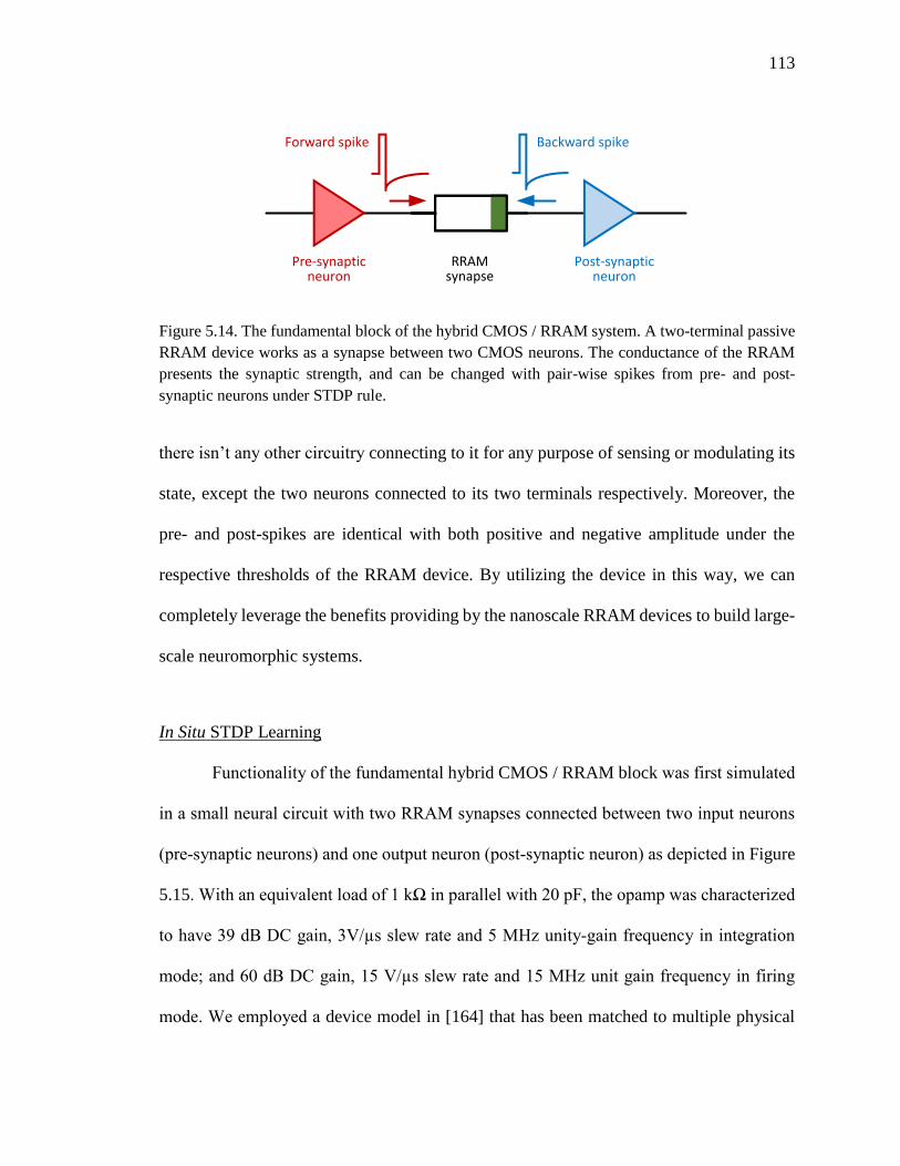
113
there isn’t any other circuitry connecting to it for any purpose of sensing or modulating its
state, except the two neurons connected to its two terminals respectively. Moreover, the
pre- and post-spikes are identical with both positive and negative amplitude under the
respective thresholds of the RRAM device. By utilizing the device in this way, we can
completely leverage the benefits providing by the nanoscale RRAM devices to build large-
scale neuromorphic systems.
In Situ STDP Learning
Functionality of the fundamental hybrid CMOS / RRAM block was first simulated
in a small neural circuit with two RRAM synapses connected between two input neurons
(pre-synaptic neurons) and one output neuron (post-synaptic neuron) as depicted in Figure
5.15. With an equivalent load of 1 kΩ in parallel with 20 pF, the opamp was characterized
to have 39 dB DC gain, 3V/µs slew rate and 5 MHz unity-gain frequency in integration
mode; and 60 dB DC gain, 15 V/µs slew rate and 15 MHz unit gain frequency in firing
mode. We employed a device model in [164] that has been matched to multiple physical
Forward spike Backward spike
Post-synapticneuron
Pre-synapticneuron
RRAMsynapse
Figure 5.14. The fundamental block of the hybrid CMOS / RRAM system. A two-terminal passive
RRAM device works as a synapse between two CMOS neurons. The conductance of the RRAM
presents the synaptic strength, and can be changed with pair-wise spikes from pre- and post-
synaptic neurons under STDP rule.
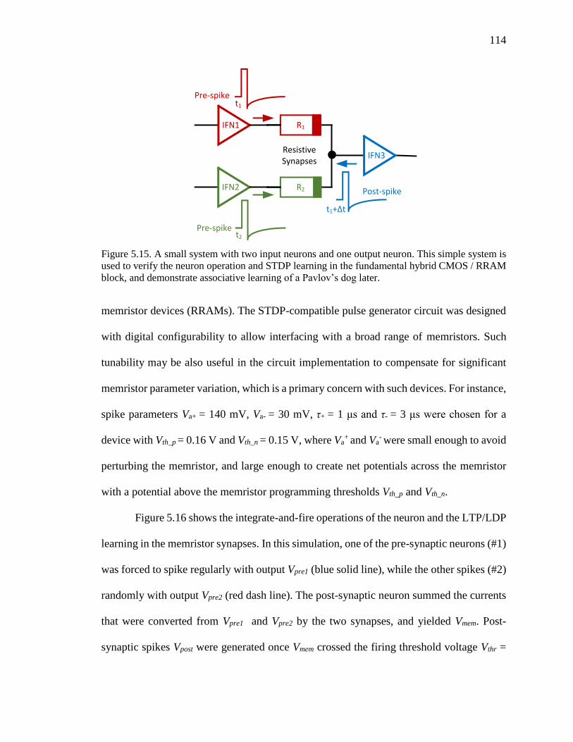
114
memristor devices (RRAMs). The STDP-compatible pulse generator circuit was designed
with digital configurability to allow interfacing with a broad range of memristors. Such
tunability may be also useful in the circuit implementation to compensate for significant
memristor parameter variation, which is a primary concern with such devices. For instance,
spike parameters Va+ = 140 mV, Va-
= 30 mV, τ+ = 1 μs and τ-
= 3 μs were chosen for a
device with Vth_p = 0.16 V and Vth_n
= 0.15 V, where Va+ and Va
- were small enough to avoid
perturbing the memristor, and large enough to create net potentials across the memristor
with a potential above the memristor programming thresholds Vth_p and Vth_n.
Figure 5.16 shows the integrate-and-fire operations of the neuron and the LTP/LDP
learning in the memristor synapses. In this simulation, one of the pre-synaptic neurons (#1)
was forced to spike regularly with output Vpre1 (blue solid line), while the other spikes (#2)
randomly with output Vpre2 (red dash line). The post-synaptic neuron summed the currents
that were converted from Vpre1 and Vpre2 by the two synapses, and yielded Vmem. Post-
synaptic spikes Vpost were generated once Vmem crossed the firing threshold voltage Vthr =
Pre-spike
Post-spike
t1
t1+Δt
ResistiveSynapses
IFN1
IFN2
R1
R2
t2
Pre-spike
IFN3
Figure 5.15. A small system with two input neurons and one output neuron. This simple system is
used to verify the neuron operation and STDP learning in the fundamental hybrid CMOS / RRAM
block, and demonstrate associative learning of a Pavlov’s dog later.
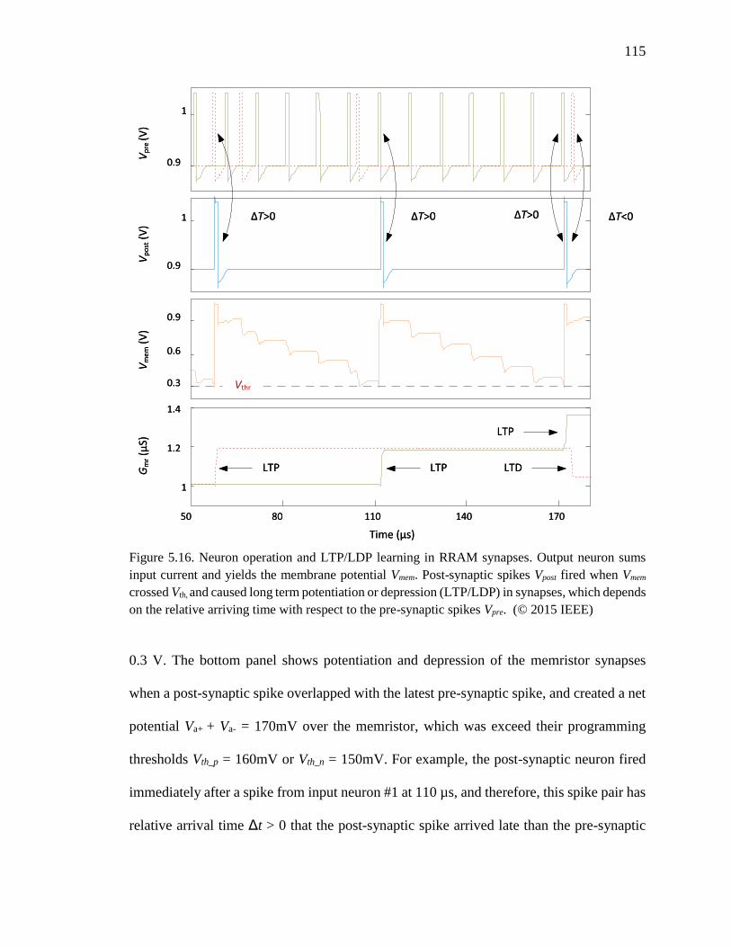
115
0.3 V. The bottom panel shows potentiation and depression of the memristor synapses
when a post-synaptic spike overlapped with the latest pre-synaptic spike, and created a net
potential Va+ + Va- = 170mV over the memristor, which was exceed their programming
thresholds Vth_p = 160mV or Vth_n = 150mV. For example, the post-synaptic neuron fired
immediately after a spike from input neuron #1 at 110 µs, and therefore, this spike pair has
relative arrival time Δt > 0 that the post-synaptic spike arrived late than the pre-synaptic
0.9
1
Vp
re (V
)
0.9
1
Vp
ost
(V
)
0.3
0.6
0.9
Vm
em (
V)
50 80 110 140 170
1
1.2
1.4
Time (µs)
Gm
r (µ
S)
0.9
1
Vp
re (V
)
0.9
1
Vp
ost
(V
)
0.3
0.6
0.9
Vm
em (
V)
50 80 110 140 170
1
1.2
1.4
Time (µs)
Gm
r (µ
S)
Vthr
LTPLTP LTPLTP
LTPLTP
LTDLTD
ΔT>0 ΔT>0 ΔT>0 ΔT>0 ΔT<0 ΔT<0 ΔT>0 ΔT>0
Figure 5.16. Neuron operation and LTP/LDP learning in RRAM synapses. Output neuron sums
input current and yields the membrane potential Vmem. Post-synaptic spikes Vpost fired when Vmem
crossed Vth, and caused long term potentiation or depression (LTP/LDP) in synapses, which depends
on the relative arriving time with respect to the pre-synaptic spikes Vpre. (© 2015 IEEE)
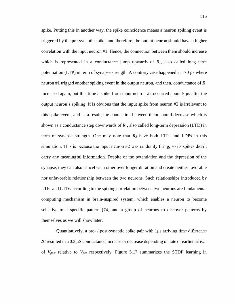
116
spike. Putting this in another way, the spike coincidence means a neuron spiking event is
triggered by the pre-synaptic spike, and therefore, the output neuron should have a higher
correlation with the input neuron #1. Hence, the connection between them should increase
which is represented in a conductance jump upwards of R1, also called long term
potentiation (LTP) in term of synapse strength. A contrary case happened at 170 µs where
neuron #1 trigged another spiking event in the output neuron, and then, conductance of R1
increased again, but this time a spike from input neuron #2 occurred about 5 μs after the
output neuron’s spiking. It is obvious that the input spike from neuron #2 is irrelevant to
this spike event, and as a result, the connection between them should decrease which is
shown as a conductance step downwards of R2, also called long-term depression (LTD) in
term of synapse strength. One may note that R2 have both LTPs and LDPs in this
simulation. This is because the input neuron #2 was randomly firing, so its spikes didn’t
carry any meaningful information. Despite of the potentiation and the depression of the
synapse, they can also cancel each other over longer duration and create neither favorable
nor unfavorable relationship between the two neurons. Such relationships introduced by
LTPs and LTDs according to the spiking correlation between two neurons are fundamental
computing mechanism in brain-inspired system, which enables a neuron to become
selective to a specific pattern [74] and a group of neurons to discover patterns by
themselves as we will show later.
Quantitatively, a pre- / post-synaptic spike pair with 1μs arriving time difference
Δt resulted in a 0.2 μS conductance increase or decrease depending on late or earlier arrival
of Vpost relative to Vpre respectively. Figure 5.17 summarizes the STDP learning in
117
memristor conductance change ΔGmr versus ±5 µs range of Δt. The asymmetric curve shape
with more depression peak value than potentiation was caused by the lower memristor
negative threshold Vth_n than Vth_p.
Example of Associative Learning
Associative learning is simple classic conditioning experimentally demonstrated by
a neural network with two input neurons for sensory and one output neurons for association
decision. Such a simple neural network is analogous to the seminal research done by Pavlov
with salivation response in dogs. Associative learning is especially important as it is
believed to be behind how brains correlate individual events and how neural networks
perform certain tasks very effectively. First proposed in [165], synaptic emulators and
specially-designed microcontroller and ADC circuitry were developed to demonstrate the
-4 -2 0 2 4
-0.2
-0.1
0
0.1
0.2
Δt (µs)
ΔG
mr (
µS)
Figure 5.17. Simulated pairwise STDP learning window around 1µS conductance and 5µs relative
time range. (© 2015 IEEE)
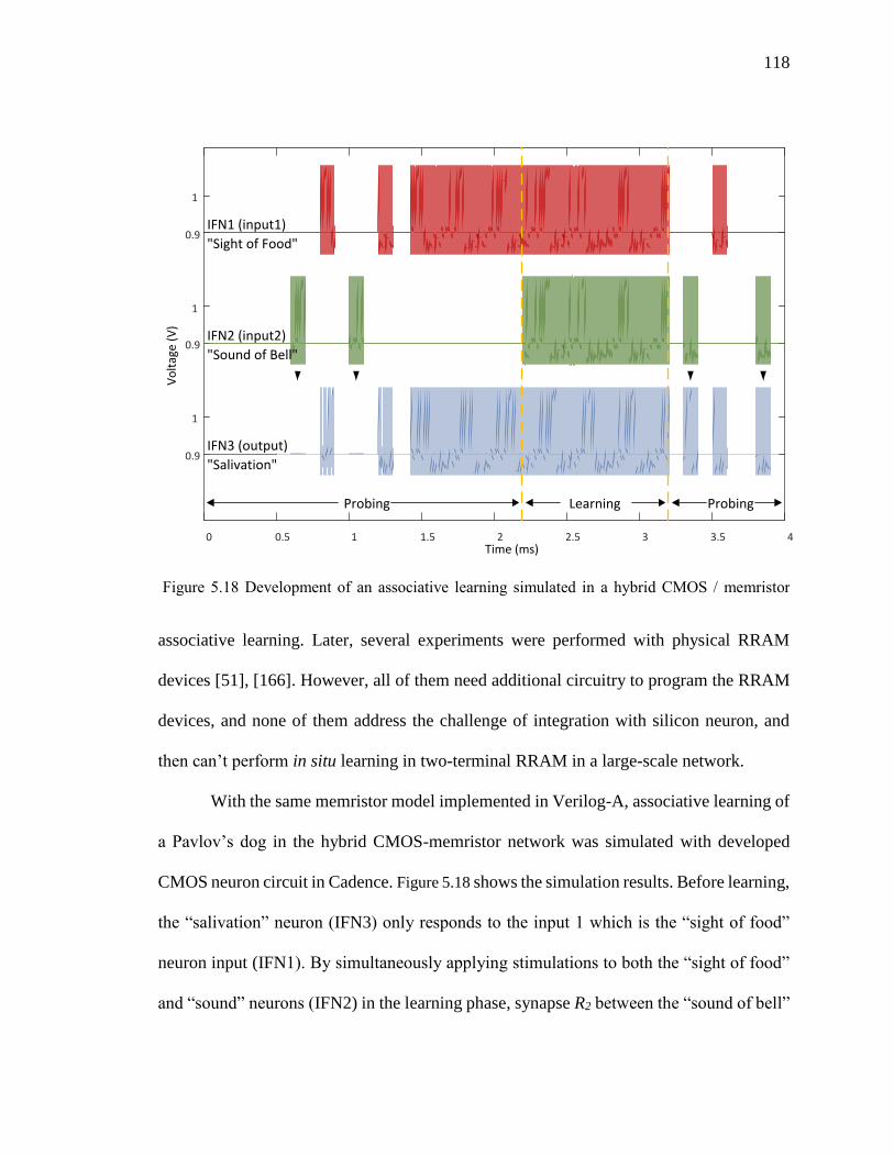
118
associative learning. Later, several experiments were performed with physical RRAM
devices [51], [166]. However, all of them need additional circuitry to program the RRAM
devices, and none of them address the challenge of integration with silicon neuron, and
then can’t perform in situ learning in two-terminal RRAM in a large-scale network.
With the same memristor model implemented in Verilog-A, associative learning of
a Pavlov’s dog in the hybrid CMOS-memristor network was simulated with developed
CMOS neuron circuit in Cadence. Figure 5.18 shows the simulation results. Before learning,
the “salivation” neuron (IFN3) only responds to the input 1 which is the “sight of food”
neuron input (IFN1). By simultaneously applying stimulations to both the “sight of food”
and “sound” neurons (IFN2) in the learning phase, synapse R2 between the “sound of bell”
0 0.5 1 1.5 2 2.5 3 3.5 4 Time (ms)
0.9
1
0.9
1
0.9
1
IFN1 (input1)
IFN2 (input2)
IFN3 (output)
"Sight of Food"
"Sound of Bell"
"Salivation"
Probing Learning Probing
Vo
ltag
e (V
)
Figure 5.18 Development of an associative learning simulated in a hybrid CMOS / memristor
Pavlov’s dog.
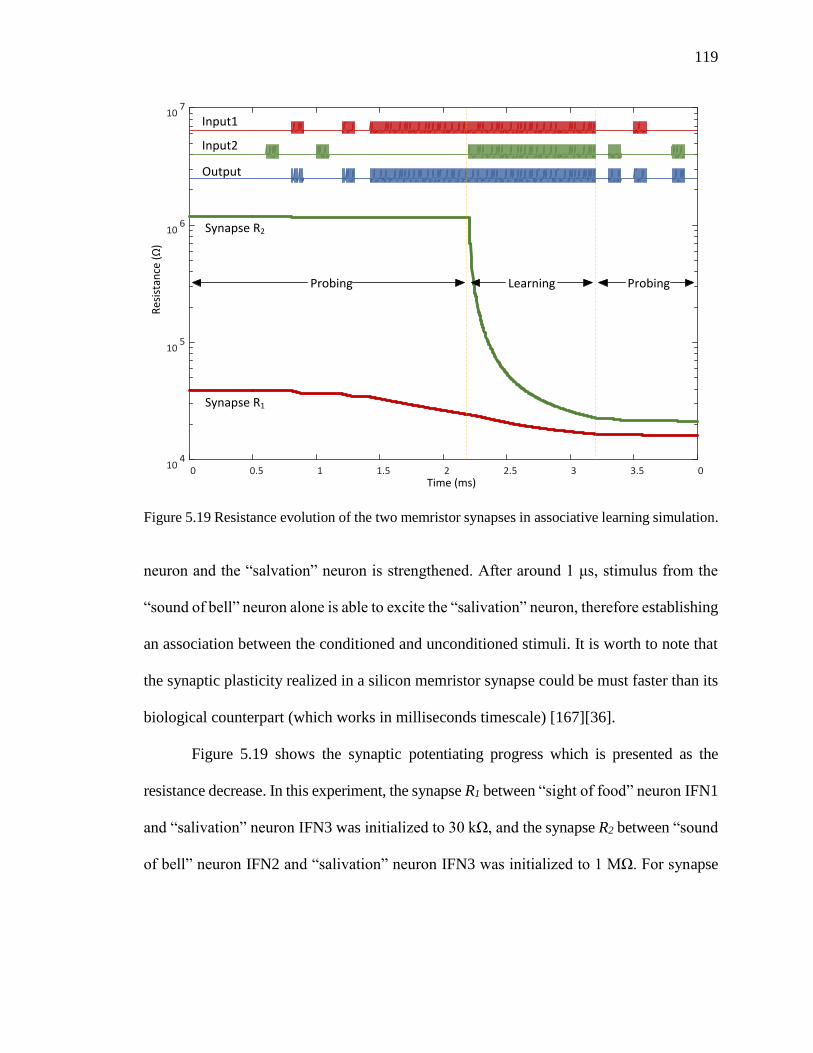
119
neuron and the “salvation” neuron is strengthened. After around 1 μs, stimulus from the
“sound of bell” neuron alone is able to excite the “salivation” neuron, therefore establishing
an association between the conditioned and unconditioned stimuli. It is worth to note that
the synaptic plasticity realized in a silicon memristor synapse could be must faster than its
biological counterpart (which works in milliseconds timescale) [167][36].
Figure 5.19 shows the synaptic potentiating progress which is presented as the
resistance decrease. In this experiment, the synapse R1 between “sight of food” neuron IFN1
and “salivation” neuron IFN3 was initialized to 30 kΩ, and the synapse R2 between “sound
of bell” neuron IFN2 and “salivation” neuron IFN3 was initialized to 1 MΩ. For synapse
0 0.5 1 1.5 2 2.5 3 3.5 0 Time (ms)
104
105
106
107
Synapse R2
Synapse R1
Probing Learning Probing
Input1
Input2
OutputR
esis
tan
ce (Ω)
Figure 5.19 Resistance evolution of the two memristor synapses in associative learning simulation.
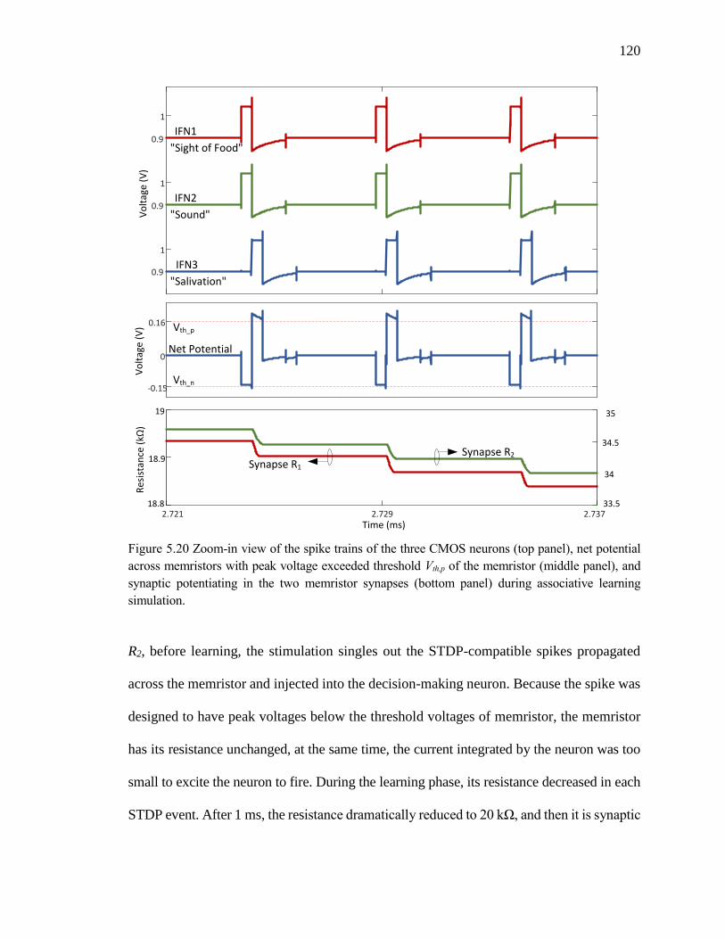
120
R2, before learning, the stimulation singles out the STDP-compatible spikes propagated
across the memristor and injected into the decision-making neuron. Because the spike was
designed to have peak voltages below the threshold voltages of memristor, the memristor
has its resistance unchanged, at the same time, the current integrated by the neuron was too
small to excite the neuron to fire. During the learning phase, its resistance decreased in each
STDP event. After 1 ms, the resistance dramatically reduced to 20 kΩ, and then it is synaptic
-0.15
0
0.16 Vth_p
Vth_n
Net Potential
2.721 2.729 2.737 Time (ms)
18.8
18.9
19
Synapse R1
Synapse R2
33.5
34
34.5
35
Vo
ltag
e (V
)R
esis
tan
ce (
kΩ)
0.9
1
0.9
1
0.9
1
IFN1
IFN2
IFN3
"Sight of Food"
"Sound"
"Salivation"
Vo
ltag
e (V
)
Figure 5.20 Zoom-in view of the spike trains of the three CMOS neurons (top panel), net potential
across memristors with peak voltage exceeded threshold Vth,p of the memristor (middle panel), and
synaptic potentiating in the two memristor synapses (bottom panel) during associative learning
simulation.
121
potentiated. In the following probing phase, larger current injected into neuron due to lower
resistance of R2 and drove the output neuron fired independently.
Figure 5.20 zooms in the in situ learning in details. Input spike from the “sight of
food” neuron causes a firing of the “salivation” neuron (contribution of spike from “sound”
neuron to output neuron firing depends on the synaptic strength between them. At the
beginning of the leaning phase, this could be neglected). A “sound” signal arrives at the
same time, in other words, is correlated to the “sight of food”. When, the spike from the
“salivation” neuron (post-synaptic spike) is simultaneous with the spike from the two
inputs neurons, then the created net potential across each memristor with peak voltage
exceeds the positive threshold voltage Vth,p. As result, the two memristor synapses
experienced an in situ modification under the STDP rule. Noting that the resistance change
of memristor depends on its state as well, modification values of the two memristor were
different. The one exhibiting high resistance decrease more than the one exhibiting lower
resistance.
Chip Implementation
To verify the proposed CMOS analog spiking neuron design and provide a platform
for on-chip RRAM integration and hybrid system-level experiment, a test chip was
planned, designed and fabricated. The test chip contains several these spiking neurons with
external tunability to optimize their response to the memristor characteristics (e.g.,
threshold voltage and the STDP program/erase pulse shape required by the fabricated
RRAM devices) and the spike shape required by learning algorithms, and an array of
bottom electrodes to provide the option for physical RRAM devices to be bonded
externally or fabricated on the CMOS chip using a back-end-of-the-line (BEOL) process.

122
For a complete chip, biasing, voltage reference, digital interface, decoupling and ESD
protection circuits were also included.
Design environment
We used Cadence Virtuoso analog design environment to do physical design work,
LVS and DRC. The chip implementation process is IBM CMOS7RF/HV AM. This process
provides 6 metal layers with a thick aluminum top metal layer. CMOS 7RF provides
standard minimum 180nm NMOS and PMOS transistors operates at 1.8V, metal-insulator-
metal (MIM) capacitors with the capacitance density from 2.05 fF/μm2 to 4.10 fF/μm2 and
several standard and optional resistors.
Neurons
The previously designed spiking neuron was implemented on the chip in full
custom manner. The opamp targets to have 39 dB DC gain, 3V/µs slew rate and 5MHz
unity-gain frequency in low power mode; while 60dB DC gain, 15MHz unit gain frequency
and 15V/µs slew rate in firing mode in full driving capability mode under 1.8 V power
supply. The two-stage folded-cascode opamp was with dynamically biased class-AB
output stage was laid out to achieve a balance between compact size and good circuit
reliability. The integration capacitor and the compensation capacitors were implemented
with MIM capacitors, and polysilicon resistors were used. The comparator was
implemented to provide less than 50ns responding time without specific size optimization.
Analog switches were implemented to provide low on-state resistance and appropriate
capacitance to enable large current flow and minimize current spur. The phase control
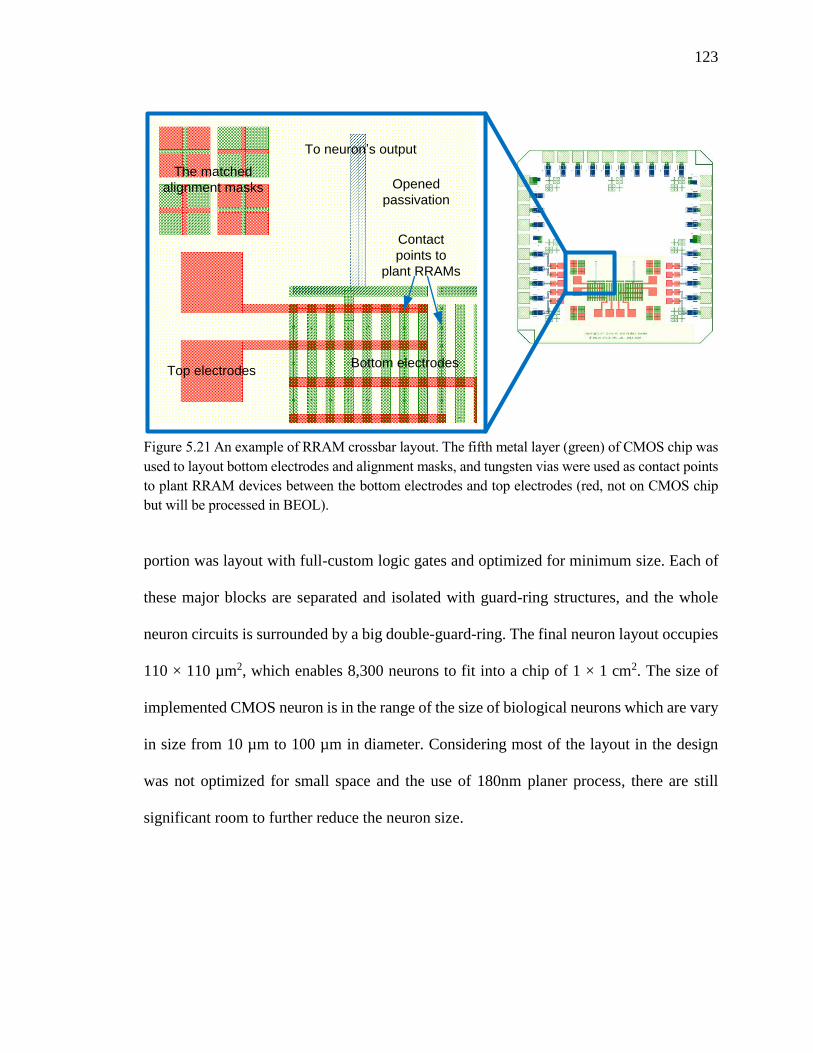
123
portion was layout with full-custom logic gates and optimized for minimum size. Each of
these major blocks are separated and isolated with guard-ring structures, and the whole
neuron circuits is surrounded by a big double-guard-ring. The final neuron layout occupies
110 × 110 µm2, which enables 8,300 neurons to fit into a chip of 1 × 1 cm2. The size of
implemented CMOS neuron is in the range of the size of biological neurons which are vary
in size from 10 µm to 100 µm in diameter. Considering most of the layout in the design
was not optimized for small space and the use of 180nm planer process, there are still
significant room to further reduce the neuron size.
The matched
alignment masks
To neuron s output
Opened
passivation
Top electrodesBottom electrodes
Contact
points to
plant RRAMs
Figure 5.21 An example of RRAM crossbar layout. The fifth metal layer (green) of CMOS chip was
used to layout bottom electrodes and alignment masks, and tungsten vias were used as contact points
to plant RRAM devices between the bottom electrodes and top electrodes (red, not on CMOS chip
but will be processed in BEOL).
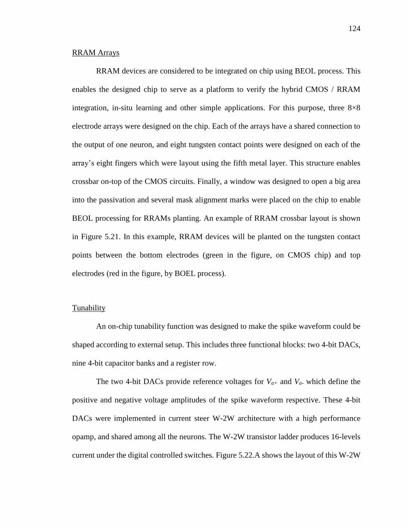
124
RRAM Arrays
RRAM devices are considered to be integrated on chip using BEOL process. This
enables the designed chip to serve as a platform to verify the hybrid CMOS / RRAM
integration, in-situ learning and other simple applications. For this purpose, three 8×8
electrode arrays were designed on the chip. Each of the arrays have a shared connection to
the output of one neuron, and eight tungsten contact points were designed on each of the
array’s eight fingers which were layout using the fifth metal layer. This structure enables
crossbar on-top of the CMOS circuits. Finally, a window was designed to open a big area
into the passivation and several mask alignment marks were placed on the chip to enable
BEOL processing for RRAMs planting. An example of RRAM crossbar layout is shown
in Figure 5.21. In this example, RRAM devices will be planted on the tungsten contact
points between the bottom electrodes (green in the figure, on CMOS chip) and top
electrodes (red in the figure, by BOEL process).
Tunability
An on-chip tunability function was designed to make the spike waveform could be
shaped according to external setup. This includes three functional blocks: two 4-bit DACs,
nine 4-bit capacitor banks and a register row.
The two 4-bit DACs provide reference voltages for Va+ and Va- which define the
positive and negative voltage amplitudes of the spike waveform respective. These 4-bit
DACs were implemented in current steer W-2W architecture with a high performance
opamp, and shared among all the neurons. The W-2W transistor ladder produces 16-levels
current under the digital controlled switches. Figure 5.22.A shows the layout of this W-2W
125
ladder. Then the current is buffered and converted into 16-levels voltages by a 72 dB, 200
MHz unity-gain frequency and 500 V/μs slew rate opamp.
To provide tunability to the positive / negative tail durations and ramp slope of the
spike waveform, three 4-bit capacitor banks were designed for each neuron. The capacitor
bank was implemented with high density MIM capacitors and organized in 4×4 common
centroid structure, as the layout shows in Figure 5.22.B. These unit capacitors are
connected in parallel under the control of digital controlled switches form a larger
capacitance with 16 levels.
Finally, a shift register row was built with DFFs with up to 3.3V input driver to
enable communication with external controller (e.g. FPGA, PC and testing instruments) to
set desired spike waveform parameters. Table 5.2 summarizes the tunable parameters of
the neuron output spike waveform as shown in Figure 5.6.A by giving the minimum and
maximum values with the increasing / decreasing step size from simulations.
A B
Figure 5.22 Layouts of (A) current steer W-2W ladder and (B) 4×4 common centroid structure MIM
capacitor bank.
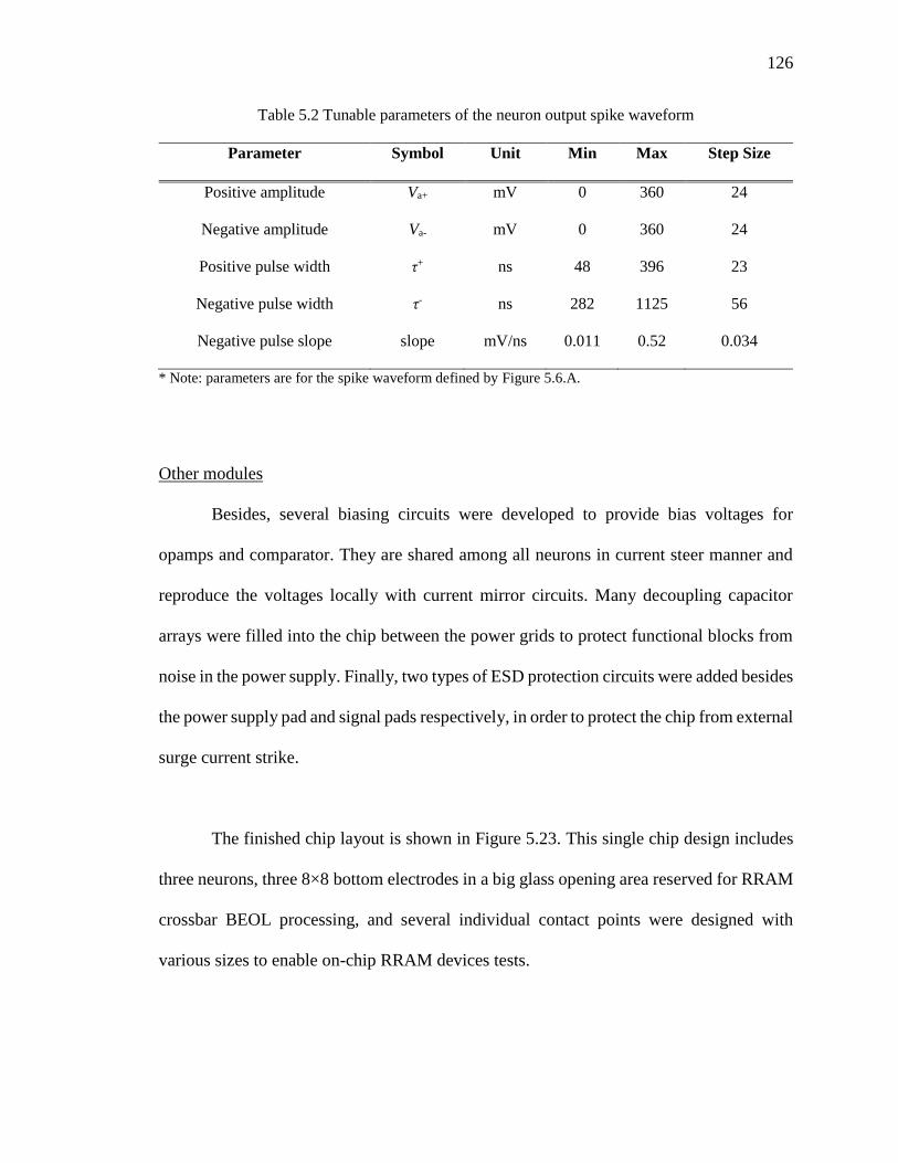
126
Other modules
Besides, several biasing circuits were developed to provide bias voltages for
opamps and comparator. They are shared among all neurons in current steer manner and
reproduce the voltages locally with current mirror circuits. Many decoupling capacitor
arrays were filled into the chip between the power grids to protect functional blocks from
noise in the power supply. Finally, two types of ESD protection circuits were added besides
the power supply pad and signal pads respectively, in order to protect the chip from external
surge current strike.
The finished chip layout is shown in Figure 5.23. This single chip design includes
three neurons, three 8×8 bottom electrodes in a big glass opening area reserved for RRAM
crossbar BEOL processing, and several individual contact points were designed with
various sizes to enable on-chip RRAM devices tests.
Table 5.2 Tunable parameters of the neuron output spike waveform
Parameter Symbol Unit Min Max Step Size
Positive amplitude Va+ mV 0 360 24
Negative amplitude Va- mV 0 360 24
Positive pulse width τ+ ns 48 396 23
Negative pulse width τ- ns 282 1125 56
Negative pulse slope slope mV/ns 0.011 0.52 0.034
* Note: parameters are for the spike waveform defined by Figure 5.6.A.
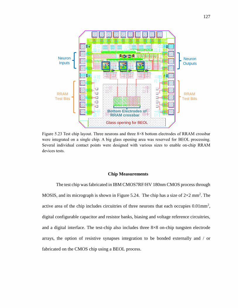
127
Chip Measurements
The test chip was fabricated in IBM CMOS7RF/HV 180nm CMOS process through
MOSIS, and its micrograph is shown in Figure 5.24. The chip has a size of 2×2 mm2. The
active area of the chip includes circuitries of three neurons that each occupies 0.01mm2,
digital configurable capacitor and resistor banks, biasing and voltage reference circuitries,
and a digital interface. The test-chip also includes three 8×8 on-chip tungsten electrode
arrays, the option of resistive synapses integration to be bonded externally and / or
fabricated on the CMOS chip using a BEOL process.
Neuron
Outputs
Neuron
Inputs
RRAM
Test Bits
Glass opening for BEOL
Bottom Electrodes of RRAM crossbar
1 2 3
RRAM
Test Bits
Figure 5.23 Test chip layout. Three neurons and three 8×8 bottom electrodes of RRAM crossbar
were integrated on a single chip. A big glass opening area was reserved for BEOL processing.
Several individual contact points were designed with various sizes to enable on-chip RRAM
devices tests.
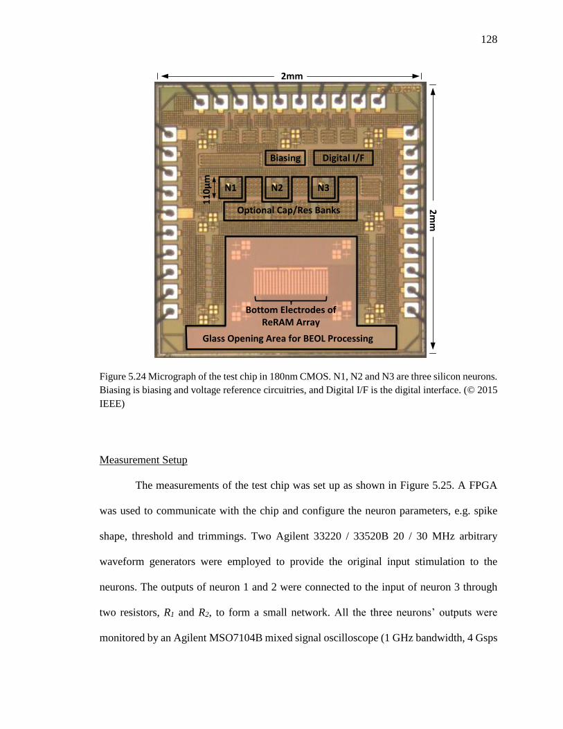
128
Measurement Setup
The measurements of the test chip was set up as shown in Figure 5.25. A FPGA
was used to communicate with the chip and configure the neuron parameters, e.g. spike
shape, threshold and trimmings. Two Agilent 33220 / 33520B 20 / 30 MHz arbitrary
waveform generators were employed to provide the original input stimulation to the
neurons. The outputs of neuron 1 and 2 were connected to the input of neuron 3 through
two resistors, R1 and R2, to form a small network. All the three neurons’ outputs were
monitored by an Agilent MSO7104B mixed signal oscilloscope (1 GHz bandwidth, 4 Gsps
Figure 5.24 Micrograph of the test chip in 180nm CMOS. N1, N2 and N3 are three silicon neurons.
Biasing is biasing and voltage reference circuitries, and Digital I/F is the digital interface. (© 2015
IEEE)
Glass Opening Area for BEOL Processing
Bottom Electrodes of ReRAM Array
N2
Biasing Digital I/F
Optional Cap/Res Banks
N1 N3
2mm
11
0µ
m
2m
m

129
sample rate, four analog channels with intrinsic 1 MΩ resistance in parallel with 14pF
capacitance). The chip was powered by a voltage regulator board which was built with
Analog Device’s ADP225 dual output adjustable low noise voltage regulator, and
connected to the main DC power supply.
Spiking Behaviors
First, the output spike trains of all the three neurons on the test chip were measured.
For this testing purpose, the output port of a neuron was connected to a driving a load with
resistance of 1 kΩ in parallel with capacitance of 20 pF which is equivalent to few
thousands of resistive synapses with 1 MΩ nominal. During the test, a 2MHz rectangular
Rpre1
FPGA
Oscilloscope
Arbitrary Waveform Generators
DC Power Supply
VDD
GND
R1
R2
IFN1out
IFN2out
IFN3out
Rpre2
IFN1in
IFN2in
IFN3in
Test
Chip
Voltage
Regulator
Figure 5.25 Setup for test chip measurements. A FPGA was used to communicate with the chip
and configure the neuron parameters (e.g. spike shape, threshold, trimming…). Two arbitrary
waveform generators were employed to provide the original input stimulation to the neurons. IFN3
was connected to the outputs of IFN1 and IFN2 through two resistors to form a small network.
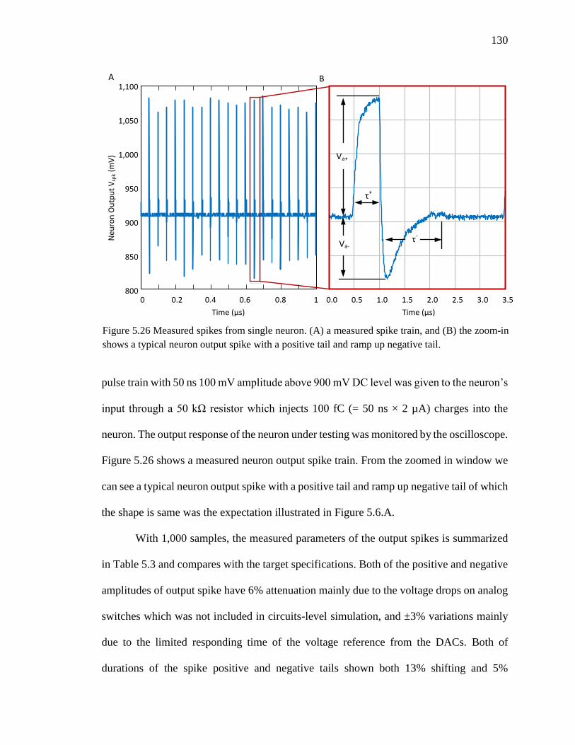
130
pulse train with 50 ns 100 mV amplitude above 900 mV DC level was given to the neuron’s
input through a 50 kΩ resistor which injects 100 fC (= 50 ns × 2 µA) charges into the
neuron. The output response of the neuron under testing was monitored by the oscilloscope.
Figure 5.26 shows a measured neuron output spike train. From the zoomed in window we
can see a typical neuron output spike with a positive tail and ramp up negative tail of which
the shape is same was the expectation illustrated in Figure 5.6.A.
With 1,000 samples, the measured parameters of the output spikes is summarized
in Table 5.3 and compares with the target specifications. Both of the positive and negative
amplitudes of output spike have 6% attenuation mainly due to the voltage drops on analog
switches which was not included in circuits-level simulation, and ±3% variations mainly
due to the limited responding time of the voltage reference from the DACs. Both of
durations of the spike positive and negative tails shown both 13% shifting and 5%
τ-
τ+
Va-
0.0 0.5 1.0 1.5 2.0 2.5 3.0 3.5
Time (µs)
Va+
0 0.2 0.4 0.6 0.8 1
Time (µs)
A
800
850
900
950
1,000
1,050
1,100
Neu
ron
Ou
tpu
t V
spk
(mV
)
B
Figure 5.26 Measured spikes from single neuron. (A) a measured spike train, and (B) the zoom-in
shows a typical neuron output spike with a positive tail and ramp up negative tail.
131
variations from the target specifications. This parameter shifting could come from the
process-voltage-temperature (PVT) related resistor variations of which only the process
variations contribute ±15%. Finally, the neurons shown approximate ±5 mV common
voltage shifting from the expected 900 mV level which are the intrinsic consequence finite
gains of the opamps.
Next, we connected one neuron’s (note as IFN1) output to another neuron’s (note
as IFN2) input to test the overlapping of the pair-wise spikes on the resistive synapse
between them. The same 2 MHz rectangular pulse train with 50 ns 100 mV amplitude
above 900 mV DC level was given to the IFN1’s input through a 50 kΩ resistor, the IFN2’s
output was still connected to a driving a load with resistance of 1 kΩ in parallel with
capacitance of 20 pF, and the IFN1 and IFN are connected with a 50 kΩ resistor. Under
this configuration, the IFN1 produced spikes same as before, while current produced by
these spikes fed into the IFN2 and caused its spiking. The spikes of IFN2 travelled in both
the forward and backward direction, while they appeared not only on neuron’s output port
but also on neuron’s input port which is connected to the IFN1. Figure 5.27 illustrates a
spike pair that was applied across the resistor connecting between IFN1 and IFN2. It shows
a relative arrival time Δt around 0.5 μs of the two paired spikes. In a 0.4 μs time-window,
the spikes created a net potential greater than the synaptic modification threshold, Vth_p =
Table 5.3 Measured Parameters of the Typical Neuron Output Spike
Parameter Symbol Unit Designed Measured
Positive amplitude Va+ mV 360 340 ± 20
Negative amplitude Va- mV 180 160 ± 20
Positive pulse width τ+ ns 396 450 ± 25
Negative pulse width τ- ns 1125 1000 ± 100
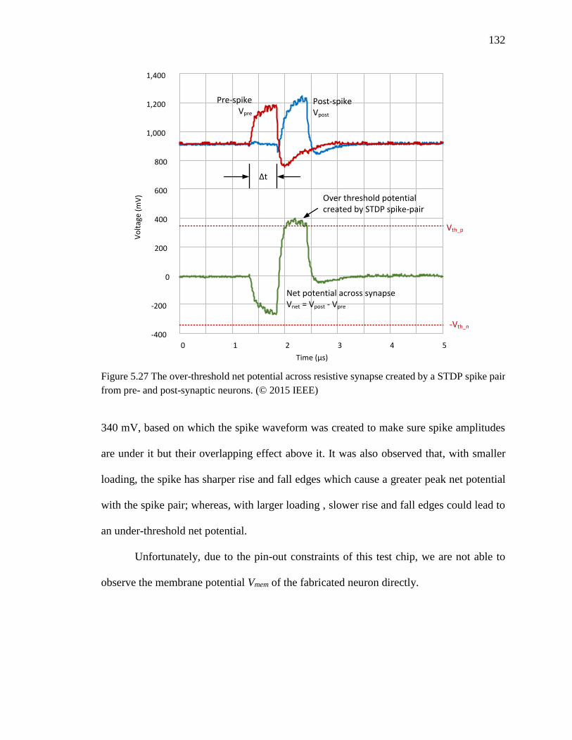
132
340 mV, based on which the spike waveform was created to make sure spike amplitudes
are under it but their overlapping effect above it. It was also observed that, with smaller
loading, the spike has sharper rise and fall edges which cause a greater peak net potential
with the spike pair; whereas, with larger loading , slower rise and fall edges could lead to
an under-threshold net potential.
Unfortunately, due to the pin-out constraints of this test chip, we are not able to
observe the membrane potential Vmem of the fabricated neuron directly.
+Vth_p
-Vth_n
Δt
-400
-200
0
200
400
600
800
1,000
1,200
1,400
0 1 2 3 4 5
Vo
ltag
e (m
V)
Time (μs)
Net potential across synapseVnet = Vpost - Vpre
Over threshold potential created by STDP spike-pair
Post-spikeVpost
Pre-spikeVpre
Figure 5.27 The over-threshold net potential across resistive synapse created by a STDP spike pair
from pre- and post-synaptic neurons. (© 2015 IEEE)
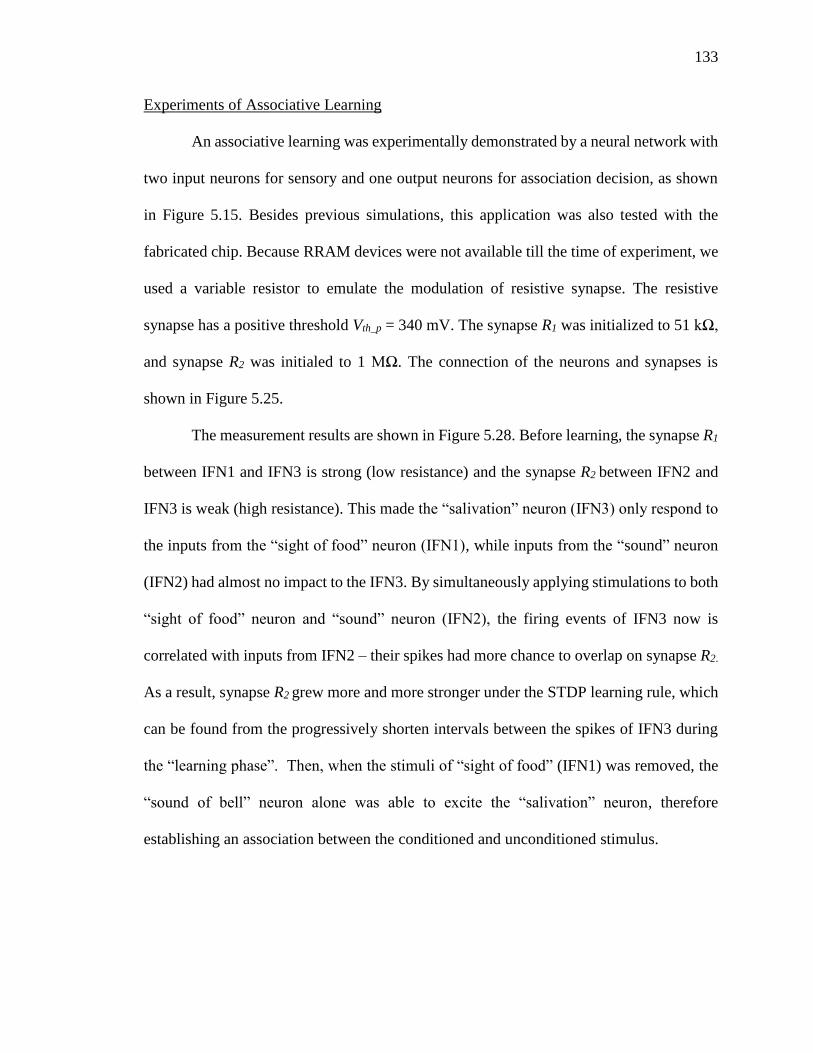
133
Experiments of Associative Learning
An associative learning was experimentally demonstrated by a neural network with
two input neurons for sensory and one output neurons for association decision, as shown
in Figure 5.15. Besides previous simulations, this application was also tested with the
fabricated chip. Because RRAM devices were not available till the time of experiment, we
used a variable resistor to emulate the modulation of resistive synapse. The resistive
synapse has a positive threshold Vth_p = 340 mV. The synapse R1 was initialized to 51 kΩ,
and synapse R2 was initialed to 1 MΩ. The connection of the neurons and synapses is
shown in Figure 5.25.
The measurement results are shown in Figure 5.28. Before learning, the synapse R1
between IFN1 and IFN3 is strong (low resistance) and the synapse R2 between IFN2 and
IFN3 is weak (high resistance). This made the “salivation” neuron (IFN3) only respond to
the inputs from the “sight of food” neuron (IFN1), while inputs from the “sound” neuron
(IFN2) had almost no impact to the IFN3. By simultaneously applying stimulations to both
“sight of food” neuron and “sound” neuron (IFN2), the firing events of IFN3 now is
correlated with inputs from IFN2 – their spikes had more chance to overlap on synapse R2.
As a result, synapse R2 grew more and more stronger under the STDP learning rule, which
can be found from the progressively shorten intervals between the spikes of IFN3 during
the “learning phase”. Then, when the stimuli of “sight of food” (IFN1) was removed, the
“sound of bell” neuron alone was able to excite the “salivation” neuron, therefore
establishing an association between the conditioned and unconditioned stimulus.
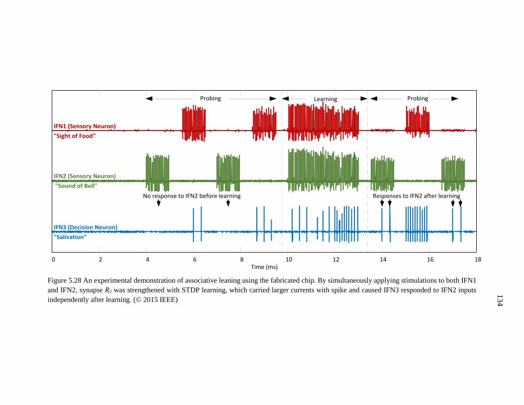
134
0 2 4 6 8 10 12 14 16 18Time (ms)
IFN1 (Sensory Neuron)
"Sight of Food"
IFN2 (Sensory Neuron)
"Sound of Bell"
IFN3 (Decision Neuron)
"Salivation"
LearningProbing Probing
Responses to IFN2 after learningNo response to IFN2 before learning
Figure 5.28 An experimental demonstration of associative leaning using the fabricated chip. By simultaneously applying stimulations to both IFN1
and IFN2, synapse R2 was strengthened with STDP learning, which carried larger currents with spike and caused IFN3 responded to IFN2 inputs
independently after learning. (© 2015 IEEE)

135
Summary
In this chapter, a compact spiking leaky integrate-and-fire CMOS neuron circuits
is presented. The proposed neuron is built upon a signle opamp which is able to configured
as a low power active inverting integrator, as well as a voltage buffer with large output
dirving capability to accommodate RRAM devices. It also employs a compact
asynchonous comparator for explicit firing threshold, and a spike generator to produce
STDP-compatible pulses. Besides, other circuit components support this reconfiguration
architecture and provide external tunablility are disscussed. Circuits simulations have
shown a network comprising of the desgined neruon and general memristive synapses can
realize STDP learning and associative learning without any additional training circuitry,
and achieved a high energy efficiency when driving a large number of resisitve syanpses.
Furthuremore, a test chip with three designed neruons and a crossbar structure for future
RRAM integration was implemended and fabricated a standard 0.18μm CMOS process.
The measurement results verified the neuron’s functionalities, and the associative learning
experiment was demonstrated sucessfully. Thanks to its unique topology and dual-mode
operation, the proposed CMOS neuron contributes a core building block to integrate dense
resistive synapses for large-scale hybrid CMOS / RRAM neuromorphic systems.
136
CHAPTER 6
GENERALIZED CMOS SPIKING NEURON AND HYBRID CMOS /
RRAM INTEGRATION FOR BRAIN-INSPIRED LEARNING
Spike-dependent synaptic plasticity is believed to be the basic mechanism that
underlies learning in a brain. In the previous chapter, experimental work with the designed
CMOS spiking neuron has revealed ways in which pair-wise spikes can change synaptic
strength by modulating conductance of the RRAM devices under the STDP rule, and a task
of auto-associative learning was performed with single post-synaptic neuron. However, to
realize more complicated tasks like pattern recognition, neurons need to work together. In
this chapter, novel CMOS neuron designs that enable local supervised and unsupervised
learning are presented. With a generalized neuron design, the system architecture that
integrates CMOS neurons with RRAM synapses is discussed. Finally, a demonstration of
real-world pattern recognition in supervised learning manner based on circuits-level
simulations is presented.
Enabling Brain-Inspired Learning
A neural network learns through synaptic plasticity in excitatory connections as
well as inhibitory connections. In a local WTA learning scheme, an inhibit signal can be
communicated to every other neuron in the network once it fires. At the same time, each
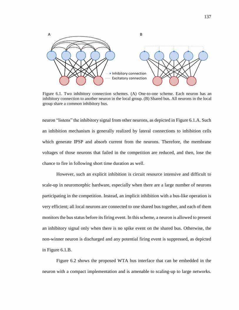
137
neuron “listens” the inhibitory signal from other neurons, as depicted in Figure 6.1.A. Such
an inhibition mechanism is generally realized by lateral connections to inhibition cells
which generate IPSP and absorb current from the neurons. Therefore, the membrane
voltages of those neurons that failed in the competition are reduced, and then, lose the
chance to fire in following short time duration as well.
However, such an explicit inhibition is circuit resource intensive and difficult to
scale-up in neuromorphic hardware, especially when there are a large number of neurons
participating in the competition. Instead, an implicit inhibition with a bus-like operation is
very efficient; all local neurons are connected to one shared bus together, and each of them
monitors the bus status before its firing event. In this scheme, a neuron is allowed to present
an inhibitory signal only when there is no spike event on the shared bus. Otherwise, the
non-winner neuron is discharged and any potential firing event is suppressed, as depicted
in Figure 6.1.B.
Figure 6.2 shows the proposed WTA bus interface that can be embedded in the
neuron with a compact implementation and is amenable to scaling-up to large networks.
Inhibitory connectionExcitatory connection
A B
Figure 6.1. Two inhibitory connection schemes. (A) One-to-one scheme. Each neuron has an
inhibitory connection to another neuron in the local group. (B) Shared bus. All neurons in the local
group share a common inhibitory bus.
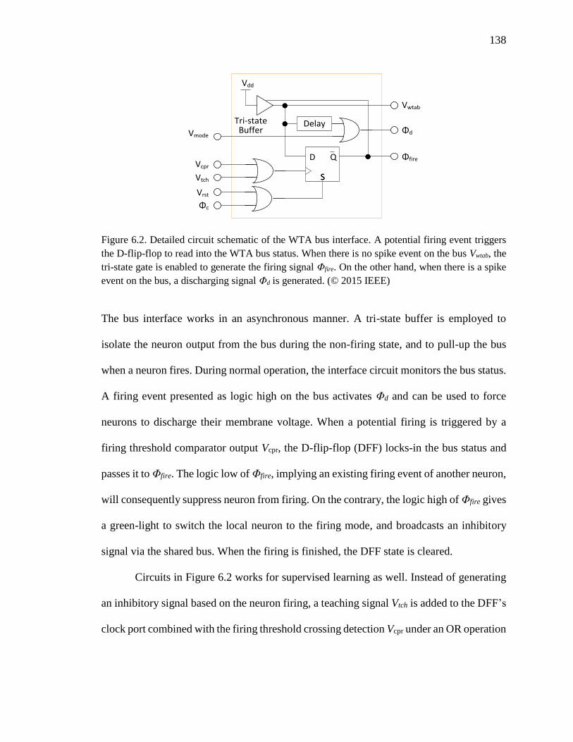
138
The bus interface works in an asynchronous manner. A tri-state buffer is employed to
isolate the neuron output from the bus during the non-firing state, and to pull-up the bus
when a neuron fires. During normal operation, the interface circuit monitors the bus status.
A firing event presented as logic high on the bus activates Φd and can be used to force
neurons to discharge their membrane voltage. When a potential firing is triggered by a
firing threshold comparator output Vcpr, the D-flip-flop (DFF) locks-in the bus status and
passes it to Φfire. The logic low of Φfire, implying an existing firing event of another neuron,
will consequently suppress neuron from firing. On the contrary, the logic high of Φfire gives
a green-light to switch the local neuron to the firing mode, and broadcasts an inhibitory
signal via the shared bus. When the firing is finished, the DFF state is cleared.
Circuits in Figure 6.2 works for supervised learning as well. Instead of generating
an inhibitory signal based on the neuron firing, a teaching signal Vtch is added to the DFF’s
clock port combined with the firing threshold crossing detection Vcpr under an OR operation
ΦfireD
SS
Vwtab
Vcpr
Vtch
VmodeΦd
Vrst
Φc
Q
Vdd
DelayTri-state Buffer
Figure 6.2. Detailed circuit schematic of the WTA bus interface. A potential firing event triggers
the D-flip-flop to read into the WTA bus status. When there is no spike event on the bus Vwtab, the
tri-state gate is enabled to generate the firing signal Φfire. On the other hand, when there is a spike
event on the bus, a discharging signal Φd is generated. (© 2015 IEEE)

139
– either crossing the firing threshold, or an external teacher can trigger a neuron to fire. At
the same time, teaching signal Vtch also applies to the Φd to trigger lateral inhibition.
Revisiting the Reconfigrable Architecture
Summarizing previous discussions to fully leverage the benefits offered by the
RRAM synapses, a silicon neuron that is amenable to network scale-up and accommodates
dense RRAM integration should:
1) Connect to a synapse at one terminal only;
2) Sustain a constant poetical across the synapses in the absence of spikes;
3) Provide a current summing node to sense incoming spikes;
4) Fire a suitable waveform to enable STDP in the synapses;
5) Be capable of providing large current that flows into synapses when firing;
6) Be compact and energy-efficient.
Now, in order to connect several neurons to form a local competitive learning, an additional
capability is required
7) Enable pattern learning through decision-making ability.
Figure 6.3 shows the schematics of a proposed CMOS neuron that fulfills the above
requirements. This circuit effectively combines an opamp-based integrator, an STDP-
compatible spike generator, a WTA interface and a control circuit for reconfiguration. By
employing tri-mode operation, it provides a unique port, Vden, to sum the incoming currents
and to propagate post-synaptic spikes, and another port Vaxon to propagate pre-synaptic
spikes. These two ports also sustain a fixed voltage Vrest during integration and membrane
capacitance discharge, while driving a specific STDP-compatible waveform with a large
current to enable online synaptic plasticity in the large number of RRAM synapses
connected in parallel. Moreover, an inhibitive discharge mode with a shared WTA bus
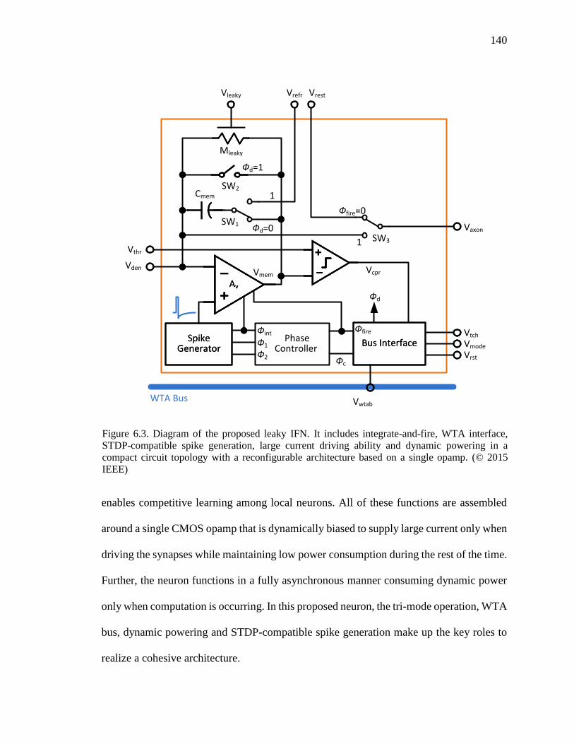
140
enables competitive learning among local neurons. All of these functions are assembled
around a single CMOS opamp that is dynamically biased to supply large current only when
driving the synapses while maintaining low power consumption during the rest of the time.
Further, the neuron functions in a fully asynchronous manner consuming dynamic power
only when computation is occurring. In this proposed neuron, the tri-mode operation, WTA
bus, dynamic powering and STDP-compatible spike generation make up the key roles to
realize a cohesive architecture.
WTA Bus
Cmem
Vthr
Vmem
Vrefr
Mleaky
SW1
SW2
AvAv
SW3
1
Фd=1
Фfire=0
1
SpikeGenerator
SpikeGenerator
Vaxon
Vden
Ф1
Ф2
Vleaky Vrest
Фint Фfire Vtch
Vmode
Фd
Vwtab
Vrst
Vcpr
Фc
Фd=0
Bus InterfaceBus Interface Phase Controller
Figure 6.3. Diagram of the proposed leaky IFN. It includes integrate-and-fire, WTA interface,
STDP-compatible spike generation, large current driving ability and dynamic powering in a
compact circuit topology with a reconfigurable architecture based on a single opamp. (© 2015
IEEE)

141
Triple-Mode Operation
A spiking silicon neuron for competitive learning should perform three major
functions: (1) current summing and integration, (2) firing when membrane potential crosses
a threshold and driving resistive loads, and (3) providing an inhibitive discharge. These
three functions are performed with a single opamp which is a key advantage of our neuron.
(1) The integration mode
As shown in Figure 6.4.A, in this mode, switch SW1 connects the “membrane” capacitor
Cmem with the output of the opamp, SW2 is open, and SW3 connects post-synapses to a rest
voltage Vrest which can be either equal to Vrest or can be floated. Φd and Φfire are
asynchronous phase signals to control the switches. As the spike generator is designed to
hold a voltage to the refractory potential Vrest during the non-firing time, the opamp’s
positive port is set to Vrest. Under this configuration, the opamp realizes a leaky integrator;
currents flowing from the pre-synapses are summed at Vden and charge the capacitor Cmem
resulting in “membrane potential” Vmem, with the voltage leak-rate controlled by a triode
transistor Mleaky. Vmem moves down as more charge is stored on Cmem, and triggers a
reconfiguration event of the neuron upon reaching the firing threshold Vthr.
(2) The firing mode
As shown in Figure 6.4.B, in this mode, switch SW2 is closed and the switch SW3 bridges
the opamp output to the post-synapses. The opamp is now reconfigured as a voltage buffer.
The STDP-compatible spike generator creates the required action potential waveform Vspk
and relays it to the positive port of the opamp. Then, both the pre-synapses and post-
synapses are shorted together to the buffer’s output, ensuring effective buffering of signals
142
in both the pre- and post-synaptic directions. The neuron propagates spikes in the backward
direction from Vden which is the same port of current summing. The pre-synaptic spikes are
driven in the forward direction on Vaxon which is the port that drives the post-synapses. This
firing-mode occurs either when the neuron wins the first-to-fire competition among the
local neurons connected to a WTA bus, or during supervised learning. In the former
scenario, the winning neuron presents a firing signal on the WTA bus noted as Vwtab, and
forces other neurons on the same bus into “discharge mode”. In the latter scenario, Vmode
indicates a supervised learning procedure and disables competition among the neurons.
Then, with a teaching signal Vtch, the neuron is forced to fire a spike and drives it into pre-
synapses, and this modulates the synaptic weights under the STDP learning rule. For stable
operation, only one Vtch of a neuron is active at a time in order to avoid conflict.
(3) The inhibitive discharge mode
As shown in Figure 6.4.C, in this mode, switch SW1 is closed, SW2 connects Vrest to
discharge Cmem, and SW3 is disconnected from the opamp output to isolate the neuron from
the post-synapses.
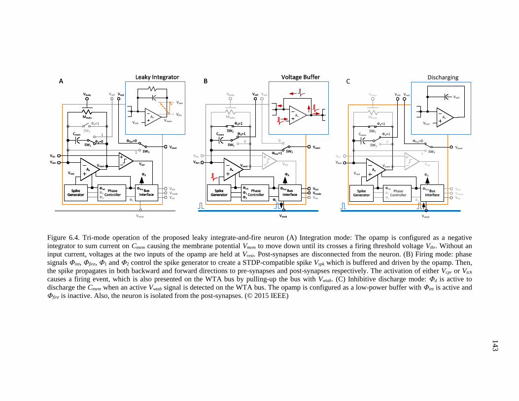
143
Cmem
Vthr
Vmem
Vrefr
Mleaky
SW1
SW2
AvAv
SW3
1
Фd=1
Фfire=0
1
SpikeGenerator
SpikeGenerator
Vaxon
Vden
Ф1
Ф2
Vleaky Vrest
Фint Фfire Vtch
Vmode
Фd
Vwtab
Vrst
Vcpr
Фc
Фd=0
Bus Interface
Bus Interface
Phase Controller
Vrest
A
Av
VrefrVmem
Vrest
Vthr
Leaky Integrator
Cmem
Vthr
Vmem
Vrefr
Mleaky
SW1
SW2
Av
SW3
1
Фd=1
Фfire=0
1
SpikeGenerator
Vaxon
Vden
Ф1
Ф2
Vleaky Vrest
Фint Фfire Vtch
Vmode
Фd
Vwtab
Vrst
Vcpr
Фc
Фd=0
Bus Interface
Phase Controller
Vrest
A
Av
VrefrVmem
Vrest
Vthr
Leaky Integrator
Cmem
Vthr
Vmem
Vrefr
Mleaky
SW1
SW2
AvAv
SW3
Фd=1
Фd=1
0
Фfire=1
SpikeGenerator
SpikeGenerator
Vaxon
Vden
Ф1
Ф2
Vleaky Vrest
Фint Фfire Vtch
Vmode
Фd
Vwtab
Vrst
Vcpr
Фc
0
Bus Interface
Bus Interface
Phase Controller
BVoltage Buffer
Av
Cmem
Vthr
Vmem
Vrefr
Mleaky
SW1
SW2
Av
SW3
Фd=1
Фd=1
0
Фfire=1
SpikeGenerator
Vaxon
Vden
Ф1
Ф2
Vleaky Vrest
Фint Фfire Vtch
Vmode
Фd
Vwtab
Vrst
Vcpr
Фc
0
Bus Interface
Phase Controller
BVoltage Buffer
Av
Cmem
Vthr
Vmem
Vrefr
Mleaky
SW1
SW2
AvAv
SW3
Фd=1
Фd=1
Фfire=0
1
Vaxon
Vden
Ф1
Ф2
Vleaky Vrest
Фint Фfire Vtch
Vmode
Фd
Vwtab
Vrst
Vcpr
Фc
0
Bus Interface
Bus Interface
Phase Controller
Vrest
CDischarging
Av
Vrest
Vrefr
SpikeGenerator
SpikeGenerator
Figure 6.4. Tri-mode operation of the proposed leaky integrate-and-fire neuron (A) Integration mode: The opamp is configured as a negative
integrator to sum current on Cmem causing the membrane potential Vmem to move down until its crosses a firing threshold voltage Vthr. Without an
input current, voltages at the two inputs of the opamp are held at Vrest. Post-synapses are disconnected from the neuron. (B) Firing mode: phase
signals Φint, Φfire, Φ1 and Φ2 control the spike generator to create a STDP-compatible spike Vspk which is buffered and driven by the opamp. Then,
the spike propagates in both backward and forward directions to pre-synapses and post-synapses respectively. The activation of either Vcpr or Vtch
causes a firing event, which is also presented on the WTA bus by pulling-up the bus with Vwtab. (C) Inhibitive discharge mode: Φd is active to
discharge the Cmem when an active Vwtab signal is detected on the WTA bus. The opamp is configured as a low-power buffer with Φint is active and
Φfire is inactive. Also, the neuron is isolated from the post-synapses. (© 2015 IEEE)
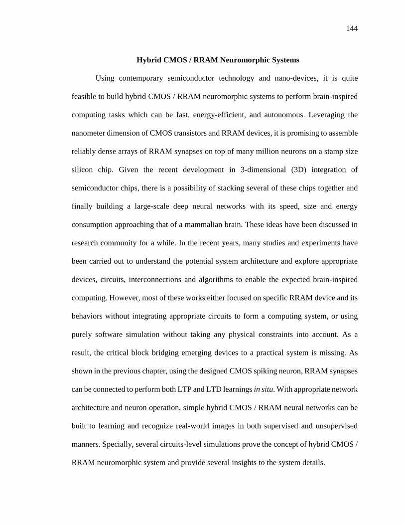
144
Hybrid CMOS / RRAM Neuromorphic Systems
Using contemporary semiconductor technology and nano-devices, it is quite
feasible to build hybrid CMOS / RRAM neuromorphic systems to perform brain-inspired
computing tasks which can be fast, energy-efficient, and autonomous. Leveraging the
nanometer dimension of CMOS transistors and RRAM devices, it is promising to assemble
reliably dense arrays of RRAM synapses on top of many million neurons on a stamp size
silicon chip. Given the recent development in 3-dimensional (3D) integration of
semiconductor chips, there is a possibility of stacking several of these chips together and
finally building a large-scale deep neural networks with its speed, size and energy
consumption approaching that of a mammalian brain. These ideas have been discussed in
research community for a while. In the recent years, many studies and experiments have
been carried out to understand the potential system architecture and explore appropriate
devices, circuits, interconnections and algorithms to enable the expected brain-inspired
computing. However, most of these works either focused on specific RRAM device and its
behaviors without integrating appropriate circuits to form a computing system, or using
purely software simulation without taking any physical constraints into account. As a
result, the critical block bridging emerging devices to a practical system is missing. As
shown in the previous chapter, using the designed CMOS spiking neuron, RRAM synapses
can be connected to perform both LTP and LTD learnings in situ. With appropriate network
architecture and neuron operation, simple hybrid CMOS / RRAM neural networks can be
built to learning and recognize real-world images in both supervised and unsupervised
manners. Specially, several circuits-level simulations prove the concept of hybrid CMOS /
RRAM neuromorphic system and provide several insights to the system details.
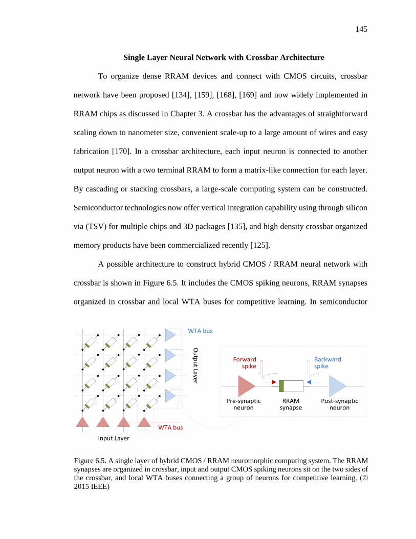
145
Single Layer Neural Network with Crossbar Architecture
To organize dense RRAM devices and connect with CMOS circuits, crossbar
network have been proposed [134], [159], [168], [169] and now widely implemented in
RRAM chips as discussed in Chapter 3. A crossbar has the advantages of straightforward
scaling down to nanometer size, convenient scale-up to a large amount of wires and easy
fabrication [170]. In a crossbar architecture, each input neuron is connected to another
output neuron with a two terminal RRAM to form a matrix-like connection for each layer.
By cascading or stacking crossbars, a large-scale computing system can be constructed.
Semiconductor technologies now offer vertical integration capability using through silicon
via (TSV) for multiple chips and 3D packages [135], and high density crossbar organized
memory products have been commercialized recently [125].
A possible architecture to construct hybrid CMOS / RRAM neural network with
crossbar is shown in Figure 6.5. It includes the CMOS spiking neurons, RRAM synapses
organized in crossbar and local WTA buses for competitive learning. In semiconductor
Forward spike
Backward spike
Post-synapticneuron
Pre-synapticneuron
RRAMsynapse
Ou
tpu
t Layer
Input Layer
WTA bus
WTA bus
Figure 6.5. A single layer of hybrid CMOS / RRAM neuromorphic computing system. The RRAM
synapses are organized in crossbar, input and output CMOS spiking neurons sit on the two sides of
the crossbar, and local WTA buses connecting a group of neurons for competitive learning. (©
2015 IEEE)
146
manufacturing practice, the RRAM crossbar can be fabricated on top of the CMOS circuits,
while for clear illustration purpose, the CMOS neurons are still arranged at one side of the
crossbar. A single layer or a stacking of multiple layers of such an architecture is expected
to work for in situ learning and real-time classifications for real-world patterns.
Example of Supervised Handwriting Digits Recognition
The Application of Optical Character Recognition
As an important application of machine learning, optical character recognition
(OCR) is widely used to demonstrate and evaluate pattern recognition performance. An
electronic OCR system is designed to convert the images of printed text into computer-
readable text to be used for electronic storage, pre-processing for machine learning, text-
to-speech, and data mining, etc. Figure 6.6 illustrates a single-layer OCR system with the
proposed architecture: the text image is read by an input sensory matrix where each pixel
maps to a neuron and is converted into spikes. All spikes from input neurons propagate
through a synaptic RRAM/memristor network to the output neurons. Summing of the input
spikes causes a spike from a winning output neuron under WTA competition, which then
back-propagates and locally updates weights of the synapses via a STDP learning rule.
Simulation Setups
To effectively train this network, a supervised learning method was used. The
teaching signal Vtch is provided to the assigned output neuron. The signal Vtch forces the
neuron to spike immediately after input pattern is received. Thus, the learning algorithm is
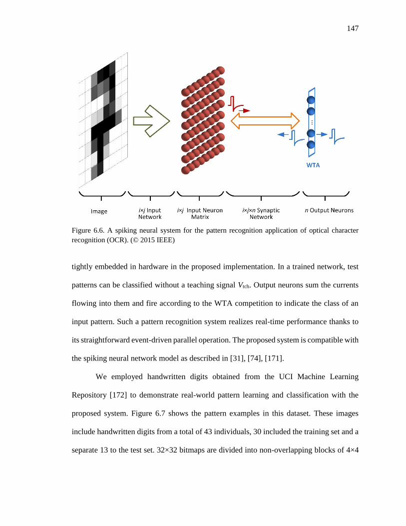
147
tightly embedded in hardware in the proposed implementation. In a trained network, test
patterns can be classified without a teaching signal Vtch. Output neurons sum the currents
flowing into them and fire according to the WTA competition to indicate the class of an
input pattern. Such a pattern recognition system realizes real-time performance thanks to
its straightforward event-driven parallel operation. The proposed system is compatible with
the spiking neural network model as described in [31], [74], [171].
We employed handwritten digits obtained from the UCI Machine Learning
Repository [172] to demonstrate real-world pattern learning and classification with the
proposed system. Figure 6.7 shows the pattern examples in this dataset. These images
include handwritten digits from a total of 43 individuals, 30 included the training set and a
separate 13 to the test set. 32×32 bitmaps are divided into non-overlapping blocks of 4×4
Figure 6.6. A spiking neural system for the pattern recognition application of optical character
recognition (OCR). (© 2015 IEEE)

148
and the number of ‘on’ pixels are counted in each block. This generates an input matrix of
8×8 where each element is an integer in the range of 0 to 15.
In our simulations, digits “0”, “1”, “2” and “7” were selected from the training
dataset, in which there are 376, 389, 380 and 387 samples of each digit respectively. In the
testing dataset, the samples number are 178, 182, 177 and 179, respectively. Samples in
the testing dataset are different from the samples in the training dataset. These images were
mapped onto an 8×8 sensory neuron matrix consists of 64 IFNs, and pixel values were
converted into currents flowing to IFNs, with a threshold of seven or greater for “on” values
used. This results in the input spike trains are shown in Fig. 8D. Each dot represents a spike
and corresponds to an image pixel in binary form.
During the training phase, the training mode Vmode signal was sent to the output
neurons. Digit samples were presented to the system in their original sequence (random)
in the dataset. Corresponding labels were read into the simulator to activate the teaching
First 20Samples
Train(random)
Test(class-by-class)
Figure 6.7. Examples of digits from UCI optical handwriting dataset.

149
signal Vtch to the corresponding output neuron, and forced a post-synaptic spike Vpost at 1μs
after each pattern was presented. All samples of the four digits in the training dataset were
presented.
Simulation Results
Figure 6.8 plots conductance changes in the RRAM synapses connecting to each of
the four output neurons. Before training, all synapses were initialized with Gaussian
randomly distributed conductance (μ = 8.5 nS, σ = 4 nS). During training, their conductance
values were gradually increased and separated to different values, due to the STDP learning
of the RRAM synapses. Because of computing resource restrictions on circuit-level
simulations, we have limited the training demonstration to only one epoch here. However,
the weights stabilize eventually after several epochs of training based on Matlab
simulations later using the LIF neuron model instead of a transistor-level circuit. Figure
6.9 is a rearrangement of the conductance into an 8×8 bitmap with each pixel corresponding
to an input image. Before training, all synapses were initialized with a Gaussian random
distributed conductance (μ = 8.5 nS, σ = 4 nS). After training, the maximum conductance
is 53 μS, and the minimum conductance is 6.6 nS. It is remarkable that the synaptic
networks extracted several distinctive features of the digits: The loop of the digit “0”, the
vertical line of the “1”, and the bone of “2” and “7”.
Figure 6.10 shows a test-case simulation with 20 samples from each digit (out of
four) and presented to the system for recognition in a class-by-class fashion. With an
untrained synaptic network, the four output neurons responded to the inputs with random
spiking. After training, each output neuron responds to the input patterns in the same class

150
most of time showing clear selectivity, and only one neuron fired under the local
competition rule.
Figure 6.11 zooms into the details of currents and membrane voltages during
testing. Due to the modulation of the synaptic network (causing different integration
speeds), the total current flowing into the output neurons were separated; the neuron with
the largest current (I0) had its membrane voltage Vmem0 cross the firing threshold Vth first
winning the competition to fire first; whereas the current flowing into neuron “7” (I7) was
too small to make its Vmem7 reach the firing threshold. The other two neurons had their Vmem
reach the firing threshold, but their potential firing events were suppressed by the winner
neuron. Membrane voltages of all neurons were reset by the WTA signal on the shared bus
(not shown), and the actual circuit behavior introduced a 50 ns delay from Vth crossing to
Vmem resetting. To illustrate this winner-takes-all in another way, we define spiking
‘opportunities’ of the output neurons based on the total currents flowing into them
𝑝𝑛 =∑ 𝐼𝑛,𝑖(𝑡) 𝑖
∑ ∑ 𝐼𝑛,𝑖(𝑡) 𝑖𝑛,
where pn is the relative spiking opportunity of the nth output neuron and In,i is the current
flowing into the nth output neuron by the ith input. With the same synaptic weights and the
all In,i equal, it follows that pn = 1/n, which means the same chance to fire and no winner
(for this reason, the synapses can’t be initialized to all zero values. And such a condition
doesn’t exist in a real-world environment too). Once the synaptic weights are well
modulated, they create different currents flowing into neurons. With a larger current, a
neuron has the higher opportunity to spike in the same timeslot, which distinguishes the
winner neuron from the others, as shown in Figure 6.12.
151
In this pattern recognition example, a 96% correction rate was achieved with the
selected 4 digits. Matlab simulations with the IFN mathematical model show 83%
correction rate with all 10 digits. These results are encouraging especially considering the
system is a simple single-layer network, and no input encoding was applied. Applying
symbolic patterns that were used in [44], [45], [48], [49], [173], [174], 100% correction
rates were achieved simply because each pattern produced a unique synaptic network with
their weights having exactly the same shape as the identical pattern of each class.
Discussions
Device Thresholds
Previous example demonstrates that the described CMOS spiking neuron
architecture is generalized for memristor synapses. By selecting appropriate CMOS
technology with sufficient supply voltage, online STDP learning can be achieved with the
memristors, but not limited to, as reported in [175]–[178]. However, the memristor in [32],
with its Vth_p = 1.5V and Vth_n
= 0.5V, would be difficult to fit into this architecture. With
these threshold voltages, it is impossible to find a STDP pulse that can produce both
potentiation and depression while not disturbing the memristor. In other words, for
generalized STDP learning, assuming symmetric the pre- and post-synaptic spikes, a
memristor is expected to have its thresholds satisfy the condition: |𝑉𝑝 − 𝑉𝑛| < 𝑚𝑖𝑛 (𝑉𝑝, 𝑉𝑛).
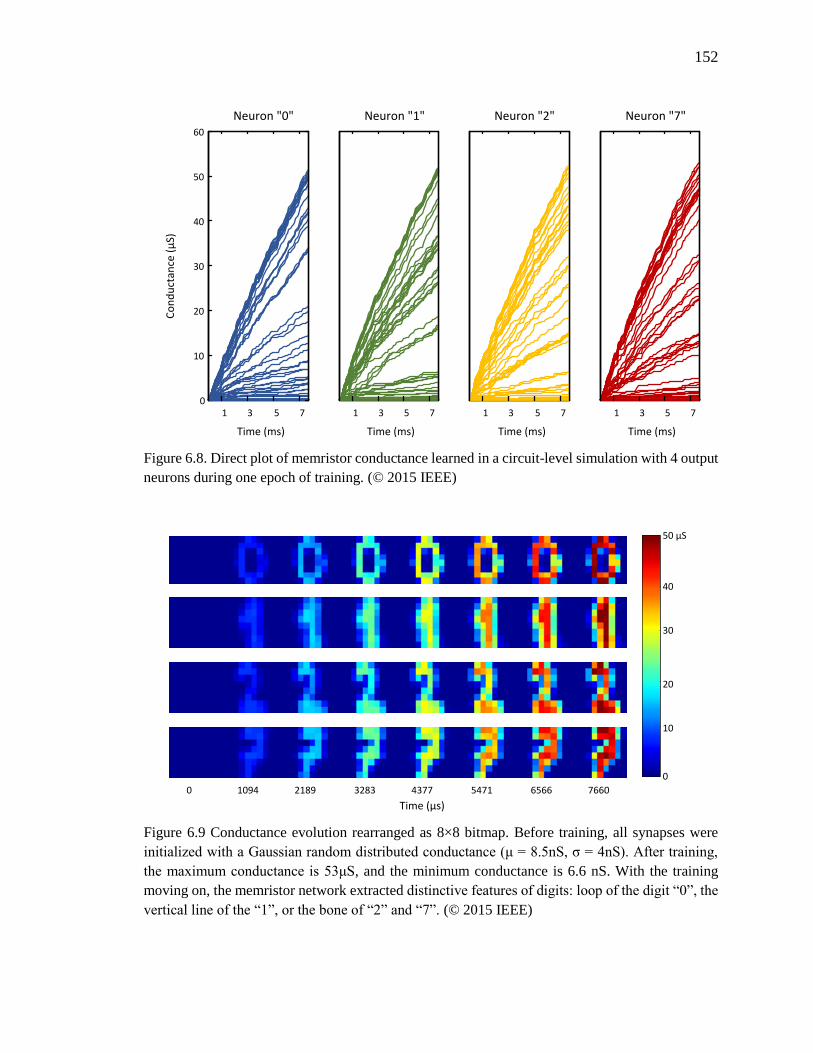
152
10
10
20
30
40
60
Neuron "0"
Time (ms)
Co
nd
uct
ance
(µ
S)
1 3 5 7
Neuron "1"
Time (ms)
Neuron "2" Neuron "7"
50
3 5 7 1
Time (ms)
3 5 7 1 3 5 7
Time (ms)
Figure 6.8. Direct plot of memristor conductance learned in a circuit-level simulation with 4 output
neurons during one epoch of training. (© 2015 IEEE)
10
20
30
40
50 µS
0 1094 2189 3283 4377 5471 6566 7660
Time (µs)
0
Figure 6.9 Conductance evolution rearranged as 8×8 bitmap. Before training, all synapses were
initialized with a Gaussian random distributed conductance (μ = 8.5nS, σ = 4nS). After training,
the maximum conductance is 53μS, and the minimum conductance is 6.6 nS. With the training
moving on, the memristor network extracted distinctive features of digits: loop of the digit “0”, the
vertical line of the “1”, or the bone of “2” and “7”. (© 2015 IEEE)
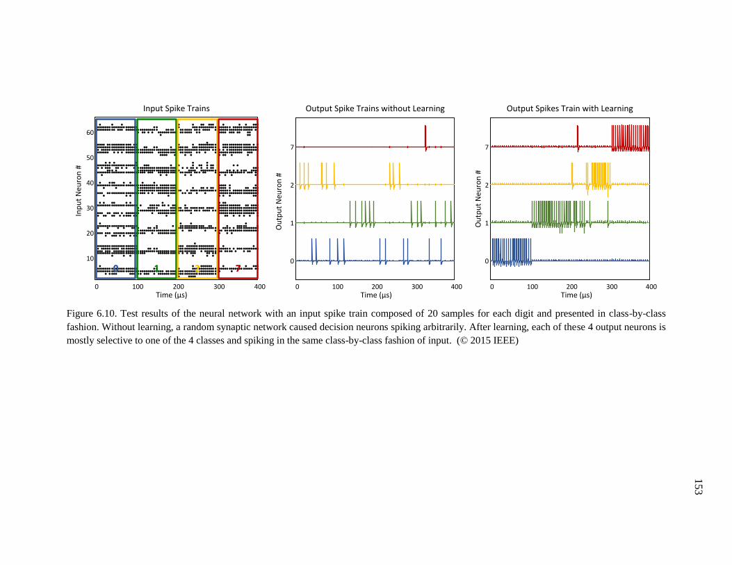
153
0 100 200 300 400
10
20
30
40
50
60
Input Spike Trains
Inp
ut
Neu
ron
#
Time (µs)0 100 200 300 400
0
1
2
7
Output Spike Trains without Learning
Ou
tpu
t N
euro
n #
Time (µs)0 100 200 300 400
0
1
2
7
Output Spikes Train with Learning
Time (µs)
0 1 2 70 1 2 7
Ou
tpu
t N
euro
n #
Figure 6.10. Test results of the neural network with an input spike train composed of 20 samples for each digit and presented in class-by-class
fashion. Without learning, a random synaptic network caused decision neurons spiking arbitrarily. After learning, each of these 4 output neurons is
mostly selective to one of the 4 classes and spiking in the same class-by-class fashion of input. (© 2015 IEEE)
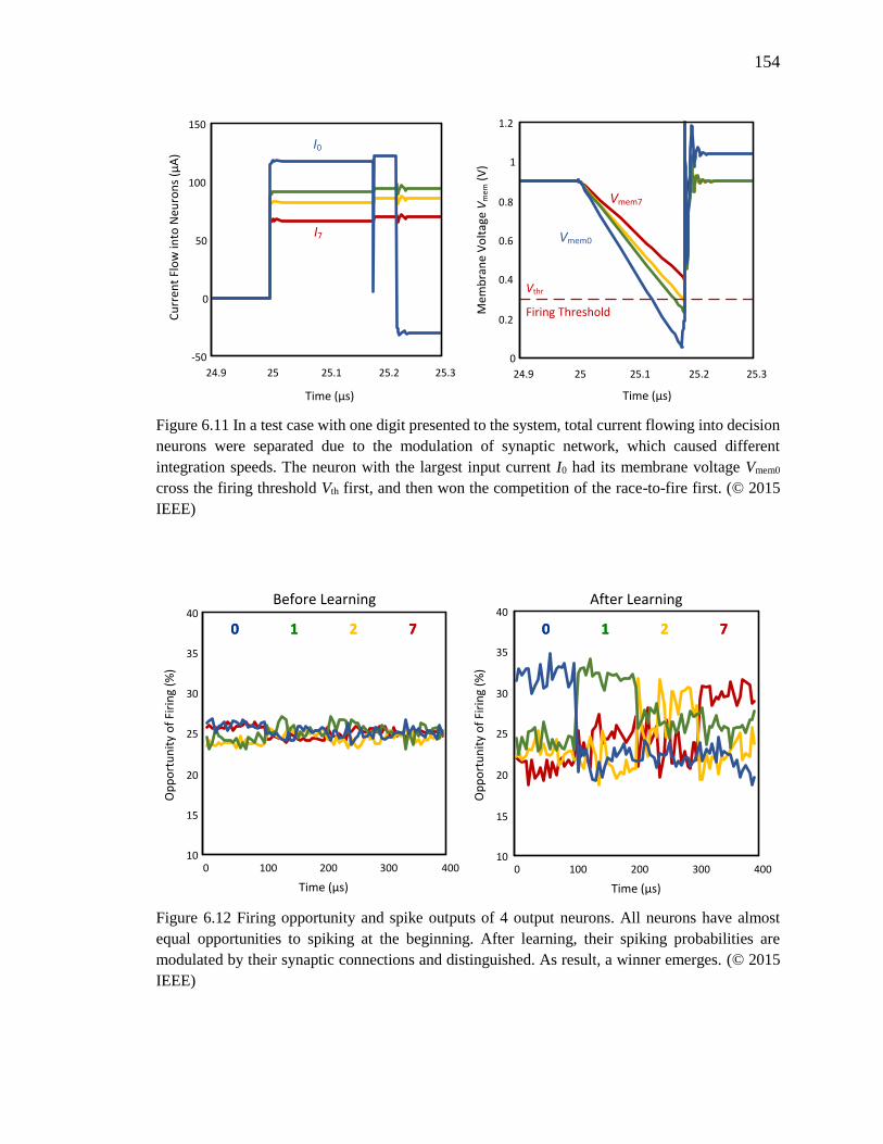
154
24.9 25 25.1 25.2 25.3
-50
0
50
100
150
Cu
rre
nt
Flo
w in
to N
eu
ron
s (µ
A)
Time (µs)
I0
I7
24.9 25 25.1 25.2 25.3
0
0.2
0.4
0.6
0.8
1
1.2
Me
mb
ran
e V
olt
age
Vm
em
(V
)
Vthr
Firing Threshold
Vmem0
Vmem7
Time (µs)
Figure 6.11 In a test case with one digit presented to the system, total current flowing into decision
neurons were separated due to the modulation of synaptic network, which caused different
integration speeds. The neuron with the largest input current I0 had its membrane voltage Vmem0
cross the firing threshold Vth first, and then won the competition of the race-to-fire first. (© 2015
IEEE)
0 100 200 300 40010
15
20
25
30
35
40Before Learning
Op
po
rtu
nit
y o
f Fi
rin
g (%
)
Time (µs)
0 100 200 300 40010
15
20
25
30
35
40After Learning
Op
po
rtu
nit
y o
f Fi
rin
g (%
)
Time (µs)
0 1 2 70 1 2 70 1 2 70 1 2 7
Figure 6.12 Firing opportunity and spike outputs of 4 output neurons. All neurons have almost
equal opportunities to spiking at the beginning. After learning, their spiking probabilities are
modulated by their synaptic connections and distinguished. As result, a winner emerges. (© 2015
IEEE)
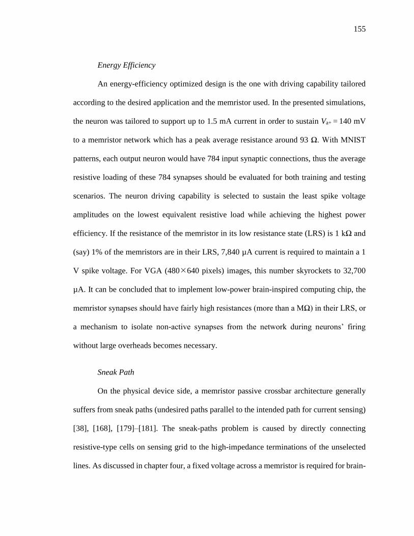
155
Energy Efficiency
An energy-efficiency optimized design is the one with driving capability tailored
according to the desired application and the memristor used. In the presented simulations,
the neuron was tailored to support up to 1.5 mA current in order to sustain Va+ = 140 mV
to a memristor network which has a peak average resistance around 93 Ω. With MNIST
patterns, each output neuron would have 784 input synaptic connections, thus the average
resistive loading of these 784 synapses should be evaluated for both training and testing
scenarios. The neuron driving capability is selected to sustain the least spike voltage
amplitudes on the lowest equivalent resistive load while achieving the highest power
efficiency. If the resistance of the memristor in its low resistance state (LRS) is 1 kΩ and
(say) 1% of the memristors are in their LRS, 7,840 µA current is required to maintain a 1
V spike voltage. For VGA (480640 pixels) images, this number skyrockets to 32,700
µA. It can be concluded that to implement low-power brain-inspired computing chip, the
memristor synapses should have fairly high resistances (more than a MΩ) in their LRS, or
a mechanism to isolate non-active synapses from the network during neurons’ firing
without large overheads becomes necessary.
Sneak Path
On the physical device side, a memristor passive crossbar architecture generally
suffers from sneak paths (undesired paths parallel to the intended path for current sensing)
[38], [168], [179]–[181]. The sneak-paths problem is caused by directly connecting
resistive-type cells on sensing grid to the high-impedance terminations of the unselected
lines. As discussed in chapter four, a fixed voltage across a memristor is required for brain-
156
inspired computing. Therefore, every path without a spike in the crossbar is tied to Vrest,
and so the above discussed large current pouring into memristor networks becomes costly
in terms of power consumption. Theoretically, a non-firing neuron could have a floating
output thus reducing the current, but consequently sneak paths may bridge spiking neurons
to other neurons and cause malfunction. So far, none of the existing solutions for sneak-
paths work for memristor synapses, and thus further studies are required.
Device Variability
Nano-scale RRAM devices show both spatial (device-to-device) variations and
temporal (trial-to-trial) variations. These variations come from limitation of fabricating
accuracy as well as the intrinsic stochastic switching behaviors of the nano-scale devices
[130], [131], [133], [182], [183]. Based on a general mathematical model fitting to
experimental results, system-level simulations revealed the typical one-layer neural
network with memristive synapses is robust to device variations under unsupervised
learning manner [52], [184]. In these simulations, 50% relative standard variations on all
the device parameters, including both spatial and temporal variations, are tolerated in
MNIST pattern classification tasks. Moreover, the work in [52] employed compound
binary memristive devices to approach multi-level RRAM and demonstrated the one-layer
neural network with WTA also tolerates to stochastic switching variations.
Although a spiking neural network offers some tolerance to device variation, the
memristor threshold variations can still fail network training when a low voltage spike is
applied. There is a careful design trade-off between the low-voltage amplitudes of a spike
required for energy-efficiency, and the high net potential margin over the memristor’s
characteristics required for reliable STDP learning. For instance, a memristor with Vth_p =
157
160 mV and Vth_n = 15 0mV requires the spike voltage must higher than 80 mV while a
practical value typically in the range of 100 to 140 mV to minimize the impact from device
variations and spike noise.
Simulations
It should be noted that the circuit-level simulations with faithful modeling of
electrical behavior consumes significant amount of time as well as computing resources.
Due to these restrictions, we limited the training demonstration to one epoch in the circuit-
level simulations in shown this work. Based on the behavioral simulation results, the
network optimally trains for the desired patterns and the weights eventually stabilize. This
is expected if the circuit-level simulations were continued for several training intervals.
Moreover, one has the flexibility to randomly initialize the weights with behavioral models.
However, in a circuits approach, the memristors are expected to ‘pre-formed’ using a
voltage pulse (or a photo-induced pre-forming step) which sets them in a high-resistance
initial state. Therefore, the circuit simulations presented were initialized with all the
memristors in their high-resistance state (low conductance) and then were potentiated to
their final weights.
Summary
This chapter presents a generalized spiking neuromorphic system. It combines
standard CMOS design of a novel silicon integrate-and-fire neuron with a RRAM crossbar
which can be realized in contemporary nano-scale semiconductor technology. This system
naturally embeds local online learning and computing by employing STDP in the RRAM
synapses and winner-take-all strategy among the local neurons. The CMOS neuron

158
assembles its functionalities in a compact manner based on a single opamp, using a tri-
mode operation, and fully exploits the synaptic density gain obtained by using RRAM
crossbar synapses. Circuit simulations verified the functionality of the proposed neuron,
and demonstrated an application of real-world pattern recognition with handwriting digits.
The described system realizes a hybrid CMOS / RRAM neural circuits block for a large-
scale brain-inspired computing architecture.
159
CHAPTER 7
CONCLUSION AND OUTLOOK
This dissertation reviews the integrated circuit elements, blocks, architectures and
methods for energy-efficient non-von-Neumann autonomous learning and computing
systems inspired from the recent understanding of biological brains, learning schemes,
architectures and nanotechnology devices. Leveraging these crucial brain-inspiration and
emerging nano-device adoption, CMOS spiking neuron designs are proposed, designed,
simulated, manufactured and measured. The designed neurons assemble the key elements
in synergistic manner and the idea of brain-like computing system was demonstrated
through detailed circuit-level simulations.
Contributions
Unique contributions of the research work described in this dissertation are
summarized as follows:
1. Proposed a compact spiking neuron architecture upon the reconfiguration of single
opamp. It realizes a leaky integrate-and-fire neuron and a voltage buffer capable of
propagating STDP-compatible spikes in both forwards and backwards directions, and
realizing in situ STDP learning in the RRAM devices.

160
2. Quantitatively analyzed the energy efficiency of the spiking neuron in driving a large
number of resistive load. Proposed a dynamic powering scheme based on the dual-
mode operation of the spiking neuron. It realized low power consumption in integration
mode and high current driving capability in firing mode. In synergy with the compact
reconfigurable neuron architecture, the proposed spiking neuron architecture is the first
silicon neuron circuit in literature that is able to accommodate dense RRAM devices as
electronics synapses for in situ STDP learning.
3. Designed the proposed spiking neuron with a standard 180-nm CMOS process.
Embedded the proposed dynamic powering techniques effectively in an opamp with a
unique minor-main branching designs. Proved that the design works as a fundamental
component for hybrid CMOS / RRAM neural network through systematic
characterization of the neuron circuits and an associative learning demonstration with
memristive synapses in circuit-level simulation.
4. Implemented and fabricated a test chip in 180nm CMOS technology containing three
of the designed CMOS spiking neurons with external tunability to the neuron
parameters and an on-chip structure for BEOL integration of RRAM crossbars.
Successfully brought up the test chip and measured the neurons’ spiking characteristics.
Demonstrated an in situ autonomous associative learning with the test chip.
5. Generalized the compact spiking neuron architecture to support local competitive
learning. Proposed the concept of shared winner-take-all (WTA) bus, and designed a
WTA interface circuitry. Developed a triple-mode operation schema for this neuron,
and systematically realized a neuron motif.
161
6. Developed a pattern learning and recognition system with the proposed neurons and
memristive synapses, and proved the proposed neuron design by successfully
demonstrating a real-world handwriting digits learning and recognition in circuit-level
simulation.
7. The generalized compact and energy efficient CMOS spiking neuron with WTA
interface and working in triple-mode operations contributes a fundamental and key
building block for dense integration of RRAM synaptic devices and online learning in
both supervised and unsupervised manner, and then, pave a path for future realization
of large-scale brain-inspired computing systems.
Discussions and Future Work
This work serves as a solid stepping stone towards realizing energy-efficient brain-
inspired computing hardware, while there are many things that remain to be investigated,
developed, and implemented.
From the systems aspect, despite most of the brain functions still remain unknown,
a lot of data and knowledge in terms of brain architecture, cortical structures, neural
microcircuits (connectomes), and neuron / synapse properties has been collected.
Understanding the implications, significance and functionalities behind these data and
knowledge will unlock significant brain-inspiration computing mechanisms, and provide
immense potential for the implementation of future intelligent computing systems. In terms
of the spiking neural networks, several works have theoretically shown its powerful
computing capability with shallow networks. However, the analysis and simulation of a
deep spiking neural network is difficult with limited computing resources. Although it has
162
been shown that synaptic parameters trained in static deep neural work can be translated
and applied to deep spiking neural network, and yield same performance as modern deep
learning system [185], the significant challenge is that there is not an effective method to
train the deep spiking neural network based on conventional algorithms. Moreover,
simulation of spiking neural network is very computationally intensive, and hence, it is
difficult to verify an idea with conventional computers. With this context, the
neuromorphic hardware that could be employed to simulate spiking neural network will
greatly accelerate pace of research and development. Recently, SpiNNaker [186] and
TrueNorth [187] have emerged as such neuromorphic hardware, and may be worth to be
widely employed in brain-inspired computing architecture studies.
From the synaptic device aspect, the research and development of nanoscale
emerging memory devices is accelerating. However, most of these work is scheduled and
planned for the traditional storage applications only; the big picture is missing in the device
studies for neuromorphic applications. Thus, a multidisciplinary research with deep
understanding of both nanotechnology and neuromorphic system is desired. For the
nanoscale device itself, the binary and stochastic switching will be a key challenge for its
usage as a synapse. Reliable device models, computing schemes and circuits topologies to
leverage these intrinsic properties are the next stepping stones to bring brain-inspired
computing system into reality. Moreover, the improvements of the nanoscale memory
devices on the energy efficiency, endurance, and hybrid and vertical integrations are
required.
In the circuits aspect, more complicated neuron design is expected with the better
understanding of the brain computation and nano-device characteristics. At the same time,

163
improvements on the total power consumption and design size are also expected. Ultra-
low power silicon neurons have been realized in sub-threshold designs, however, these
neurons don’t accommodate RRAM devices due to weak capabilities to sustain stable
current summation node and drive large resistive load. Innovations are desired here to
create more compact and energy efficient neuron architecture and designs. For large–scale
system development, the interconnections, including the internal communication, inter-
chip communications, power supply grid and reference voltages reproduction, must be
studied. For internal and inter-chip communications, address event presentation (AER)
[149] is one of the possible methods. AER encodes the spike events of a group of neurons
into asynchronous digital signals which can travel to far away destinations in a digital bus.
In AER encoder, each valid bus date represents an index (address) of the neuron which just
emit a spike; while in the decoder, a spike is reproduced and assigned to the destination
neurons according to the decoding result. Using such kind of an analog-to-digital
conversion, spiking event can be transmitted through a long distance, and then, enables
inter-chip communication. The discussions of AER’s topologies, arbitration and timing
designs can be found in [149].
In conclusion, the development of brain-inspired neuromorphic computing systems
is in its early stage, but have great potentials to be the solution to the grant computing
challenges the human society facing nowadays. The success of the development relies on
well interdisciplinary collaborations among neuroscience, material science, computer
science and electrical engineering, where the progress in each of these fields could inspire
research and development in the other fields, and then, form a synergy to tackle one and

164
another challenges. And this journey itself is a dreaming one for every scientist and
engineer.
165
REFERENCES
[1] D. Wooden, M. Malchano, K. Blankespoor, A. Howardy, A. A. Rizzi, and M. Raibert,
“Autonomous navigation for BigDog,” Proc. - IEEE Int. Conf. Robot. Autom., pp. 4736–
4741, 2010.
[2] Q. V. Le, M. Ranzato, R. Monga, M. Devin, K. Chen, G. S. Corrado, J. Dean, and A. Y.
Ng, “Building High-level Features Using Large Scale Unsupervised Learning,” in IEEE
International Conference on Machine Learning (ICML), 2012, pp. 8595–8598.
[3] R. Ananthanarayanan, S. K. Esser, H. D. Simon, and D. S. Modha, “The cat is out of the
bag: cortical simulations with 109 neurons, 1013 synapses,” in Conference on High
Performance Computing Networking, Storage and Analysis, 2009, no. c, pp. 1–12.
[4] J. Von Neumann and M. D. Godfrey, “First Draft of a Report on the EDVAC,” IEEE Ann.
Hist. Comput., vol. 15, no. 4, pp. 27–75, 1993.
[5] W. S. McCulloch and W. Pitts, “A logical calculus of the ideas immanent in nervous
activity,” Bull. Math. Biophys., vol. 5, no. 4, pp. 115–33, 1943.
[6] F. Rosenblatt, “The perceptron: a probabilistic model for information storage and
organization in the brain,” Psychol. Rev., vol. 65, no. 6, p. 386, 1958.
[7] The Economist, “After Moore’s Law: Double, Double, Toil and Trouble,” The Economist,
2016.
[8] S. H. Fuller and L. I. Millett, Eds., The Future of Computing Performance: Game Over or
Next Level? National Academies Press, 2011.
[9] G. Jarboe, “VidCon 2015 Haul: Trends, Strategic Insights & Tactical Advice,” 2015.
[10] SIA/SRC, “Rebooting the IT Revolution: A Call to Action,” 2015.
[11] IDC, “The Digital Universe,” 2012.
[12] Gartner, “Gartner Says Global Smartphone Sales to Only Grow 7 Per Cent in 2016,” 2016.
[13] M. P. Mills, “The Cloud Begins With Coal,” 2013.
[14] “Top 500 Supercomputer Sites.” [Online]. Available: www.top500.org.
[15] CNET, “Facebook stocks data center with phones from yesteryear,” 2016.
[16] “World’s Top Ddata Centers.” [Online]. Available: http://worldstopdatacenters.com/.
[17] E. J. Nowak, “Maintaining the benefits of CMOS scaling when scaling bogs down,” IBM J.
Res. Dev., vol. 46, no. 2/3, pp. 169–180, 2002.
[18] ICT, “ICT Energy Strategic Research Agenda,” 2016.
[19] G. McFarland and M. Flynn, “Limits of Scaling MOSFETs,” 1995.
[20] E. Stromatias, F. Galluppi, C. Patterson, and S. Furber, “Power analysis of large-scale, real-
time neural networks on SpiNNaker,” in International Joint Conference on Neural
Networks (IJCNN), 2013, pp. 1–8.
166
[21] W. Gerstner, R. Kempter, J. L. van Hemmen, and H. Wagner, “A neuronal learning rule for
sub-millisecond temporal coding,” Nature, vol. 383, no. 6595, pp. 76–81, 1996.
[22] G. Q. Bi and M. M. Poo, “Synaptic modifications in cultured hippocampal neurons:
dependence on spike timing, synaptic strength, and postsynaptic cell type,” J. Neurosci.,
vol. 18, no. 24, pp. 10464–72, Dec. 1998.
[23] G. Bi and M. Poo, “Synaptic modification by correlated activity: Hebb’s postulate
revisited,” Annu. Rev. Neurosci., vol. 24, pp. 139–166, 2001.
[24] P. J. Sjöström, G. G. Turrigiano, and S. B. Nelson, “Rate, timing, and cooperativity jointly
determine cortical synaptic plasticity,” Neuron, vol. 32, no. 6, pp. 1149–64, Dec. 2001.
[25] N. Golding, N. Staff, and N. Spruston, “Dendritic spikes as a mechanism for cooperative
long-term potentiation,” Nature, vol. 418, no. July, 2002.
[26] Y. Dan and M.-M. Poo, “Spike timing-dependent plasticity of neural circuits,” Neuron, vol.
44, no. 1, pp. 23–30, Sep. 2004.
[27] Y. Dan and M. Poo, “Spike timing-dependent plasticity: from synapse to perception,”
Physiol. Rev., pp. 1033–1048, 2006.
[28] T. Masquelier and S. J. S. Thorpe, “Unsupervised learning of visual features through spike
timing dependent plasticity,” PLOS Comput. Biol., vol. 3, no. 2, p. e31, Feb. 2007.
[29] U. Weidenbacher and H. Neumann, “Unsupervised learning of head pose through spike-
timing dependent plasticity,” in Perception in Multimodal Dialogue Systems, vol. 5078
LNCS, Springer Berlin Heidelberg, 2008, pp. 123–131.
[30] H. Lee, “Unsupervised Feature Learning Via Sparse Hierarchical Representations,” Thesis
Diss., no. August, p. 118, 2010.
[31] B. Nessler, M. Pfeiffer, L. Buesing, and W. Maass, “Bayesian computation emerges in
generic cortical microcircuits through spike-timing-dependent plasticity,” PLOS Comput.
Biol., vol. 9, no. 4, Apr. 2013.
[32] S. H. Jo, T. Chang, I. Ebong, B. B. Bhadviya, P. Mazumder, and W. Lu, “Nanoscale
memristor device as synapse in neuromorphic systems,” Nano Lett., vol. 10, no. 4, pp. 1297–
301, Apr. 2010.
[33] D. Kuzum, R. R. G. D. Jeyasingh, B. Lee, and H. P. Wong, “Nanoelectronic Programmable
Synapses Based on Phase Change Materials for Brain-Inspired Computing,” Nano Lett.,
vol. 12, pp. 2179–2186, 2012.
[34] S. Yu, Y. Wu, and R. Jeyasingh, “An electronic synapse device based on metal oxide
resistive switching memory for neuromorphic computation,” IEEE Transations Electron
Devices, vol. 58, no. 8, pp. 2729–2737, 2011.
[35] K. Seo, I. Kim, S. Jung, M. Jo, S. Park, J. Park, J. Shin, K. P. Biju, J. Kong, K. Lee, B. Lee,
and H. Hwang, “Analog memory and spike-timing-dependent plasticity characteristics of a
nanoscale titanium oxide bilayer resistive switching device,” Nanotechnology, vol. 22, no.
25, p. 254023, Jun. 2011.
[36] Y. Li, Y. Zhong, L. Xu, J. Zhang, X. Xu, H. Sun, and X. Miao, “Ultrafast synaptic events
in a chalcogenide memristor.,” Sci. Rep., vol. 3, p. 1619, Jan. 2013.
[37] V. Saxena, “Memory Controlled Circuit System and Apparatus,” US patent application
14/538,600 (Unpublished), 2014.
[38] J. J. Yang, D. B. Strukov, and D. R. Stewart, “Memristive devices for computing,” Nat.
Nanotechnol., vol. 8, no. 1, pp. 13–24, Jan. 2013.
167
[39] T. Chang, Y. Yang, and W. Lu, “Building Neuromorphic Circuits with Memristive
Devices,” IEEE Circuits Syst. Mag., vol. 13, no. 2, pp. 56–73, 2013.
[40] T. Serrano-Gotarredona, T. Prodromakis, and B. Linares-Barranco, “A proposal for hybrid
memristor-CMOS spiking neuromorphic learning systems,” IEEE Circuits Syst. Mag., vol.
13, no. 2, pp. 74–88, 2013.
[41] G. Indiveri, B. B. Linares-Barranco, R. Legenstein, G. Deligeorgis, and T. Prodromakis,
“Integration of nanoscale memristor synapses in neuromorphic computing architectures.,”
Nanotechnology, vol. 24, no. 38, p. 384010, 2013.
[42] S. Saïghi, C. G. Mayr, T. Serrano-Gotarredona, H. Schmidt, G. Lecerf, J. Tomas, J. Grollier,
S. Boyn, A. F. Vincent, D. Querlioz, S. La Barbera, F. Alibart, D. Vuillaume, O. Bichler,
C. Gamrat, and B. Linares-Barranco, “Plasticity in memristive devices for spiking neural
networks,” Front. Neurosci., vol. 9, 2015.
[43] D. Querlioz, W. Zhao, and P. Dollfus, “Bioinspired networks with nanoscale memristive
devices that combine the unsupervised and supervised learning approaches,” in
International Symposium on Nanoscale Architectures (NANOARCH), 2012, pp. 203–210.
[44] F. Alibart, E. Zamanidoost, and D. B. Strukov, “Pattern classification by memristive
crossbar circuits using ex situ and in situ training.,” Nat. Commun., vol. 4, no. May, p. 2072,
Jan. 2013.
[45] M. Chu, B. Kim, S. Park, H. Hwang, M.-G. Jeon, B. H. Lee, and B.-G. Lee, “Neuromorphic
Hardware System for Visual Pattern Recognition with Memristor Array and CMOS
Neuron,” IEEE Trans. Ind. Electron., vol. 62, no. 4, pp. 2410 – 2419, 2014.
[46] S. Yu, “Orientation Classification by a Winner-Take-All Network with Oxide RRAM based
Synaptic Devices,” in IEEE International Symposium on Circuits and Systems (ISCAS),
2014, pp. 1058–1061.
[47] D. Chabi, Z. Wang, W. Zhao, and J.-O. Klein, “On-chip supervised learning rule for ultra
high density neural crossbar using memristor for synapse and neuron,” in International
Symposium on Nanoscale Architectures (NANOARCH), 2014, pp. 7–12.
[48] A. Sheri, H. Hwang, M. Jeon, and B. Lee, “Neuromorphic character recognition system with
two PCMO-Memristors as a synapse,” IEEE Trans. Ind. Electron., vol. 61, no. 6, pp. 2933–
2941, 2014.
[49] P. Sheridan, W. Ma, and W. Lu, “Pattern Recognition with Memristor Networks,” in IEEE
International Symposium on Circuits and Systems (ISCAS), 2014, pp. 1078–1081.
[50] M. Payvand, J. Rofeh, A. Sodhi, and L. Theogarajan, “A CMOS-memristive self-learning
neural network for pattern classification applications,” in International Symposium on
Nanoscale Architectures (NANOARCH), 2014, no. 1, pp. 92–97.
[51] K. Moon, S. Park, J. Jang, D. Lee, J. Woo, E. Cha, S. Lee, J. Park, J. Song, Y. Koo, and H.
Hwang, “Hardware implementation of associative memory characteristics with analogue-
type resistive-switching device,” Nanotechnology, vol. 25, no. 49, p. 495204, 2014.
[52] J. Bill and R. Legenstein, “A compound memristive synapse model for statistical learning
through STDP in spiking neural networks,” Front. Neurosci., vol. 8, no. December, pp. 1–
18, 2014.
[53] C. Zamarreño-Ramos, L. A. Camuñas-Mesa, J. A. Pérez-Carrasco, T. Masquelier, T.
Serrano-Gotarredona, and B. Linares-Barranco, “On spike-timing-dependent-plasticity,
memristive devices, and building a self-learning visual cortex,” Front. Neurosci., vol. 5, no.
March, p. 26, Jan. 2011.
168
[54] T. Serrano-Gotarredona and B. Linares-Barranco, “Design of adaptive nano/CMOS neural
architectures,” in IEEE International Conference on Electronics, Circuits and Systems
(ICECS), 2012, pp. 949–952.
[55] G. Lecerf, J. Tomas, and S. Saighi, “Excitatory and Inhibitory Memristive Synapses for
Spiking Neural Networks,” in IEEE International Symposium on Circuits and Systems
(ISCAS), 2013, pp. 1616–1619.
[56] G. Lecerf and J. Tomas, “Silicon Neuron dedicated to Memristive Spiking Neural
Networks,” in IEEE International Symposium on Circuits and Systems (ISCAS), 2014, pp.
1568–1571.
[57] J. B. Reece, L. A. Urry, M. L. Cain, S. Wasserman, A. P. V. Minorsky, and R. B. Jackso,
Campbell Biology. Benjamin Cumming, 2010.
[58] S. Behnke, “Hierarchical Neural Networks for Image Interpretation,” 2003.
[59] E. R. Kandel, J. H. Schwartz, T. M. Jessell, S. A. Siegelbaum, and A. J. Hudspeth, Principle
of Neural Science. The McGraw-Hill Companies, Inc, 2013.
[60] A. Hodgkin and A. Huxley, “A quantitative description of membrane current and its
application to conduction and excitation in nerve,” J. Physiol., vol. 117, pp. 500–544, 1952.
[61] A. A. T. Nere, “Complex Neural Computation with Simple Digital Neurons,” Thesis Diss.,
2013.
[62] E. M. Izhikevich, “Simple model of spiking neurons,” IEEE Trans. Neural Networks, vol.
14, no. 6, pp. 1569–72, Jan. 2003.
[63] D. O. Hebb, The organization of behavior: A neuropsychological approach. John Wiley &
Sons, 1949.
[64] P. Dayan and L. F. Abbott, Theoretical neuroscience. Cambridge, MA: MIT Press, 2001.
[65] A. K. Jain, J. C. Mao, and K. M. Mohiuddin, “Artificial neural networks: A tutorial,”
Computer (Long. Beach. Calif)., vol. 29, no. 3, pp. 31–43, 1996.
[66] W. Gerstner, R. Ritz, and J. L. van Hemmen, “Why spikes? Hebbian learning and retrieval
of time-resolved excitation patterns,” Biol. Cybern., vol. 69, no. 5–6, pp. 503–15, Jan. 1993.
[67] H. Markram, “Regulation of Synaptic Efficacy by Coincidence of Postsynaptic APs and
EPSPs,” Science (80-. )., vol. 275, no. 5297, pp. 213–215, Jan. 1997.
[68] L. F. L. Abbott, S. B. S. Nelson, and L. F. L. Abbott, “Synaptic plasticity: taming the beast,”
Nat. Neurosci., vol. 3, no. 11, pp. 1178–183, 2000.
[69] S. Song, K. D. Miller, and L. F. Abbott, “Competitive Hebbian learning through spike-
timing-dependent synaptic plasticity,” Nat. Neurosci., vol. 3, no. 9, pp. 919–926, 2000.
[70] R. Kempter, W. Gerstner, and J. L. Van Hemmen, “Hebbian learning and spiking neurons,”
Phys. Rev. E, vol. 59, no. 4, p. 4498, 1999.
[71] S. Song, K. D. K. Miller, and L. F. Abbott, “Competitive Hebbian learning through spike-
timing-dependent synaptic plasticity,” Nat. Neurosci., vol. 3, no. 9, pp. 919–926, 2000.
[72] R. Kempter, W. Gerstner, and J. L. Van Hemmen, “Intrinsic stabilization of output rates by
spike-based Hebbian learning,” Neural Comput., vol. 13, no. 12, pp. 2709–2741, 2001.
[73] H. Markram, W. Gerstner, and P. J. Sjöström, “Spike-timing-dependent plasticity: a
comprehensive overview,” Front. Synaptic Neurosci., vol. 4, no. July, p. 2, Jan. 2012.
[74] T. Masquelier, R. Guyonneau, and S. J. Thorpe, “Spike timing dependent plasticity finds
169
the start of repeating patterns in continuous spike trains,” PLoS One, vol. 3, no. 1, p. e1377,
Jan. 2008.
[75] H. Markram, W. Gerstner, and P. J. Sjöström, “A history of spike-timing-dependent
plasticity,” Front. Synaptic Neurosci., vol. 3, no. August, p. 4, Jan. 2011.
[76] S. Haykin, Neural Networks: A Comprehensive Foundation. New York: MacMillan College
Publishing Company, 1994.
[77] T. Masquelier and G. Deco, “Learning and Coding in Neural Networks,” Princ. Neural
Coding, pp. 513–526, 2013.
[78] D. Kappel, B. Nessler, and W. Maass, “STDP Installs in Winner-Take-All Circuits an
Online Approximation to Hidden Markov Model Learning,” PLOS Comput. Biol., vol. 10,
no. 3, p. e1003511, 2014.
[79] M. Minsky and S. Papert, Perceptrons. 1969.
[80] S. Grossberg, “Contour enhancement, short-term memory, and constancies in reverberating
neural networks,” Stud. Appl. Math., vol. 52, pp. 213–257, 1973.
[81] D. E. Rumelhart, G. E. Hinton, and R. J. Williams, “Learning representations by back-
propagating errors,” Cogn. Model., vol. 5, no. 3, 1986.
[82] G. Cybenko, “Approximations by superpositions of sigmoidal functions,” Math. Control.
Signals, Syst., vol. 2, no. 4, pp. 303–314, 1989.
[83] Y. LeCun, B. Boser, J. S. Denker, D. Henderson, R. E. Howard, W. Hubbard, and L. D.
Jackel, “Backpropagation Applied to Handwritten Zip Code Recognition,” Neural
Computation, vol. 1, no. 4. pp. 541–551, 1989.
[84] C. Mead, Analog VLSI and Neural Systems. Boston, MA: Addison-Wesley Longman
Publishing Co., Inc., 1989.
[85] D. H. Hubel and T. N. Wiese, “Receptive fields, binocular interaction and functional
architecture in the cat’s visual corte,” J. Physiol., vol. 160, no. 1, pp. 106–154, 1962.
[86] T. Serre, “Hierarchical models of the visual system,” in Encyclopedia of Computational
Neuroscience, 2015, pp. 1309–1318.
[87] M. Riesenhuber and T. Poggio, “Hierarchical models of object recognition in cortex,” Nat.
Neurosci., vol. 2, no. 11, pp. 1019–25, Nov. 1999.
[88] H. Wersing and E. Körner, “Learning optimized features for hierarchical models of
invariant object recognition,” Neural Comput., vol. 15, no. 7, pp. 1559–1588, 2003.
[89] S. Ullman, “Object recognition and segmentation by a fragment-based hierarchy,” Trends
Cogn. Sci., vol. 11, no. 2, pp. 58–64, 2007.
[90] N. Pinto, D. Doukhan, J. J. DiCarlo, and D. D. Cox, “A high-throughput screening approach
to discovering good forms of biologically inspired visual representation,” PLoS Comput.
Biol., vol. 5, no. 11, 2009.
[91] A. J. Bell and T. J. Sejnowski, “The ‘independent components’ of natural scenes are edge
filters,” Vision Res., vol. 37, no. 23, pp. 3327–3338, 1997.
[92] A. Delorme, L. Perrinet, S. Thorpe, and M. Samuelides, “Network of integrate-and-fire
neurons using Rank Order Coding B: spike timing dependant plasticity and emergence of
orientation selectivity.,” Neurocomputing, vol. 38–40, no. 1–4, pp. 539–45, 2001.
[93] T. Poggio and T. Serre, “Models of visual cortex,” Scholarpedia, vol. 8, no. 4, p. 3516,
2013.
170
[94] K. Fukushima, “Neocognitron: A self-organizing neural network model for a mechanism of
pattern recognition unaffected by shift in position,” Biol. Cybern., vol. 36, no. 4, pp. 193–
202, 1980.
[95] Y. LeCun, L. Bottou, Y. Bengio, and P. Haffner, “Gradient Based Learning Applied to
Document Recognition,” Proc. IEEE, vol. 86, no. 11, pp. 2278–2324, 1998.
[96] S. Hochreiter, “Gradient flow in recurrent nets: the difficulty of learning long-term
dependencies,” in A Field Guide to Dynamical Recurrent Neural Networks, S. C. Kremer
and J. F. Kolen, Eds. IEEE Press, 2001.
[97] J. J. Schmidhuber, “Learning Complex, Extended Sequences Using the Principle of History
Compression,” Neural Comput., vol. 4, no. 2, pp. 234–242, 1992.
[98] X. Glorot, A. Bordes, and Y. Bengio, “Deep Sparse Rectifier Neural Networks,” Aistats,
vol. 15, pp. 315–323, 2011.
[99] P. Simard, D. Steinkraus, and J. Platt, “Best practices for convolutional neural networks
applied to visual document analysis,” in International Conference on Document Analysis
and Recognition (ICDAR), 2003, vol. 1, pp. 958–963.
[100] L. Deng and D. Yu, “Deep Learning: Methods and Applications,” 2014.
[101] A. Chen, “A review of emerging non-volatile memory (NVM) technologies and
applications,” Solid. State. Electron., 2016.
[102] O. Leon and L. O. Chua, “Memristor-The Missing Circuit Element,” IEEE Trans. Circuit
Theory, vol. c, no. 5, 1971.
[103] T. Prodromakis, C. Toumazou, and L. Chua, “Two centuries of memristors,” Nat. Mater.,
vol. 11, no. 6, pp. 478–481, 2012.
[104] H.-S. P. Wong, S. Raoux, S. Kim, J. Liang, J. P. Reifenberg, B. Rajendran, M. Asheghi, and
K. E. Goodson, “Phase Change Memory,” Proc. IEEE, vol. 98, no. 12, pp. 2201–2227,
2010.
[105] B. Jackson and B. Rajendran, “Nanoscale electronic synapses using phase change devices,”
ACM J. Emerg. Technol. Comput. Syst., vol. 9, no. 2, pp. 1–20, 2013.
[106] D. H. Kang, H. G. Jun, K. C. Ryoo, H. Jeong, and H. Sohn, “Emulation of spike-timing
dependent plasticity in nano-scale phase change memory,” Neurocomputing, vol. 155, pp.
153–158, 2015.
[107] A. Pantazi, S. Woźniak, T. Tuma, and E. Eleftheriou, “All-memristive neuromorphic
computing with level-tuned neurons,” Nanotechnology, vol. 27, no. 35, p. 355205, 2016.
[108] X. Fong, Y. Kim, K. Yogendra, D. Fan, A. Sengupta, A. Raghunathan, and K. Roy, “Spin-
Transfer Torque Devices for Logic and Memory: Prospects and Perspectives,” IEEE Trans.
Comput. Des. Integr. Circuits Syst., vol. 35, no. 1, pp. 1–22, 2016.
[109] P. Krzysteczko, “The Memristive Magnetic Tunnel Junction as a Nanoscopic Synapse-
Neuron System,” Adv. Mater., vol. 24, no. 6, pp. 762–6, Feb. 2012.
[110] A. F. Vincent, J. Larroque, N. Locatelli, N. Ben Romdhane, O. Bichler, C. Gamrat, W. S.
Zhao, J. O. Klein, S. Galdin-Retailleau, and D. Querlioz, “Spin-transfer torque magnetic
memory as a stochastic memristive synapse for neuromorphic systems,” IEEE Trans.
Biomed. Circuits Syst., vol. 9, no. 2, pp. 166–174, 2015.
[111] B. Rajendran and F. Alibart, “Neuromorphic Computing Based on Emerging Memory
Technologies,” IEEE J. Emerg. Sel. Top. Circuits Syst., vol. 6, no. 2, pp. 198–211, 2016.
171
[112] T.-C. Chang, K.-C. Chang, T.-M. Tsai, T.-J. Chu, and S. M. Sze, “Resistance random access
memory,” Mater. Today, vol. 00, no. 00, pp. 1–11, 2015.
[113] S. Yu, Resistive Random Access Memory (RRAM), vol. 2, no. 5. 2016.
[114] RainerWaser, D. Ielmini, H. Akinaga, H. Shima, H.-S. PhilipWong, J. J. Yang, and S. Yu,
“Introduction to Nanoionic Elements for Information Technology,” in Resisitve Switching:
From Fundamentals of Nanoionic Redox Processes to Memristive Device Applications, D.
Ielmini and R. Waser, Eds. John Wiley & Sons, 2015.
[115] D. S. Jeong, B. J. Choi, and C. S. Hwang, “Electroforming Processes in Metal Oxide
Resistive-Switching Cells,” in Resisitve Switching: From Fundamentals of Nanoionic
Redox Processes to Memristive Device Applications, D. Ielmini and R. Waser, Eds. John
Wiley & Sons, 2015.
[116] M. N. Kozicki, MariaMitkova, and I. Valov, “Electrochemical Metallization Memories,” in
Resisitve Switching: From Fundamentals of Nanoionic Redox Processes to Memristive
Device Applications, D. Ielmini and R. Waser, Eds. John Wiley & Sons, 2015.
[117] I. Valov, R. Waser, J. R. Jameson, and M. N. Kozicki, “Electrochemical metallization
memories--fundamentals, applications, prospects,” Nanotechnology, vol. 22, no. 25, p.
254003, 2011.
[118] E. Souchier, F. D ’acapito, P. Noé, P. Blaise, M. Bernard, and V. Jousseaume, “The role of
the local chemical environment of Ag on the resistive switching mechanism of conductive
bridging random access memories,” Phys. Chem. Chem. Phys., vol. 17, no. 17, pp. 23931–
23937, 2015.
[119] S. La Barbera, D. Vuillaume, F. Alibart, S. La Barbera, D. Vuillaume, and F. Alibart,
“Filamentary Switching: Synaptic Plasticity through Device Volatility,” ACS Nano, vol. 9,
no. 1, pp. 941–9, 2015.
[120] S. Mandal, A. El-Amin, K. Alexander, B. Rajendran, and R. Jha, “Novel synaptic memory
device for neuromorphic computing,” Sci. Rep., vol. 4, p. 5333, Jan. 2014.
[121] Y. Li, Y. Zhong, J. Zhang, L. Xu, Q. Wang, H. Sun, H. Tong, X. Cheng, and X. Miao,
“Activity-dependent synaptic plasticity of a chalcogenide electronic synapse for
neuromorphic systems,” Sci. Rep., vol. 4, p. 4906, Jan. 2014.
[122] S. B. Laughlin, R. R. de Ruyter van Steveninck, and J. C. Anderson, “The metabolic cost
of neural information,” Nat. Neurosci., vol. 1, no. 1, pp. 36–41, 1998.
[123] J. J. J. Harris, R. Jolivet, and D. Attwell, “Synaptic Energy Use and Supply,” Neuron, vol.
75, no. 5, pp. 762–777, 2012.
[124] B. Gao, Y. Bi, H. Y. Chen, R. Liu, P. Huang, B. Chen, L. Liu, X. Liu, S. Yu, H. S. P. Wong,
and J. Kang, “Ultra-low-energy three-dimensional oxide-based electronic synapses for
implementation of robust high-accuracy neuromorphic computation systems,” ACS Nano,
vol. 8, no. 7, pp. 6998–7004, 2014.
[125] Intel and Micron, “Intel and Micron produce breakthrough memory technology,” Intel
Website, 2015. [Online]. Available: http://newsroom.intel.com/.
[126] M. Yu, Y. Cai, Z. Wang, Y. Fang, Y. Liu, Z. Yu, Y. Pan, Z. Zhang, J. Tan, X. Yang, M. Li,
and R. Huang, “Novel Vertical 3D Structure of TaO x - based RRAM with Self-localized
Switching Region by Sidewall Electrode Oxidation,” Sci. Rep., vol. 6, no. November 2015,
pp. 1–10, 2016.
[127] S. Yu, B. Gao, Z. Fang, H. Yu, J. Kang, and H.-S. S. P. Wong, “A low energy oxide-based
172
electronic synaptic device for neuromorphic visual systems with tolerance to device
variation,” Adv. Mater., vol. 25, no. 12, pp. 1774–1779, Mar. 2013.
[128] C. Ribrault, K. Sekimoto, and A. Triller, “From the stochasticity of molecular processes to
the variability of synaptic transmission.,” Nat. Rev. Neurosci., vol. 12, no. 7, pp. 375–87,
2011.
[129] K. Moon, E. Cha, J. Park, S. Gi, K. Baek, B. Lee, S. Oh, and H. Hwang, “Analog Synapse
Device with 5-bit MLC and Improved Data Retention for Neuromorphic System,” IEEE
Electron Device Lett., vol. 37, no. 8, pp. 1–1, 2016.
[130] A. Chen and M. R. Lin, “Variability of resistive switching memories and its impact on
crossbar array performance,” in International Reliability Physics Symposium, 2011, pp.
843–846.
[131] R. Soni, P. Meuffels, G. Staikov, R. Weng, C. Kgeler, A. Petraru, M. Hambe, R. Waser, and
H. Kohlstedt, “On the stochastic nature of resistive switching in Cu doped Ge 0.3Se0.7
based memory devices,” J. Appl. Phys., vol. 110, no. 5, pp. 0–10, 2011.
[132] S. Yu, B. Gao, Z. Fang, H. Yu, J. Kang, and H.-S. P. Wong, “Stochastic learning in oxide
binary synaptic device for neuromorphic computing,” Front. Neurosci., vol. 7, no. October,
p. 186, 2013.
[133] S. Gaba, P. Sheridan, J. Zhou, S. Choi, and W. Lu, “Stochastic memristive devices for
computing and neuromorphic applications,” Nanoscale, vol. 5, pp. 5872–8, 2013.
[134] K. K. K. Likharev, “Hybrid CMOS/Nanoelectronic Circuits: Opportunities and
Challenges,” J. Nanoelectron. Optoelectron., vol. 3, no. May, pp. 203–230, Dec. 2008.
[135] M. Motoyoshi, “Through-Silicon Via (TSV),” Proc. IEEE, vol. 97, pp. 43–48, 2009.
[136] C. Kugeler, M. Meier, R. Rosezin, S. Gilles, and R. Waser, “High density 3D memory
architecture based on the resistive switching effect,” Solid. State. Electron., vol. 53, no. 12,
pp. 1287–1292, 2009.
[137] F. Chen, J. Y. Seok, and C. S. Hwang, “Integration Technology and Cell Design,” in
Resisitve Switching: From Fundamentals of Nanoionic Redox Processes to Memristive
Device Applications, D. Ielmini and R. Waser, Eds. John Wiley & Sons, 2015.
[138] M. Mahowald and R. Douglas, “A silicon neuron,” Nature, vol. 354, no. 6354, pp. 515–8,
1991.
[139] R. Edwards and G. Cauwenberghs, “Synthesis of log-domain filters from first-order
building blocks,” Analog Integr. Circuits Signal …, vol. 186, pp. 177–186, 2000.
[140] V. Rangan and A. Ghosh, “A subthreshold aVLSI implementation of the Izhikevich simple
neuron model,” in IEEE Engineering in Medicine and Biology Conference, 2010.
[141] A. Van Schaik, C. Jin, A. McEwan, and T. J. Hamilton, “A log-domain implementation of
the Izhikevich neuron model,” in IEEE International Symposium on Circuits and Systems
(ISCAS), 2010, no. 4, pp. 4253–4256.
[142] A. Van Schaik, C. Jin, A. McEwan, and T. J. Hamilton, “A log-domain implementation of
the Mihalas-Niebur neuron model,” in IEEE International Symposium on Circuits and
Systems (ISCAS), 2010, pp. 4253–4256.
[143] K. Boahen, “Retinomorphic vision systems: Reverse engineering the vertebrate retina,”
1997.
[144] J. Arthur and K. Boahen, “Recurrently connected silicon neurons with active dendrites for
one-shot learning,” in International Joint Conference on Neural Networks (IJCNN), 2004.
173
[145] C. Bartolozzi and G. Indiveri, “Synaptic dynamics in analog VLSI,” Neural Comput., vol.
19, no. 10, pp. 2581–2603, 2007.
[146] G. Indiveri, R. Etienne-Cummings, J. Schemmel, G. Cauwenberghs, J. Arthur, S. Saighi, T.
Serrano-Gotarredona, J. Wijekoon, Y. Wang, K. Boahen, B. Linares-Barranco, T. J.
Hamilton, A. van Schaik, R. Etienne-Cummings, T. Delbruck, S.-C. Liu, P. Dudek, P.
Häfliger, S. Renaud, J. Schemmel, G. Cauwenberghs, J. Arthur, K. Hynna, F. Folowosele,
S. Saighi, T. Serrano-Gotarredona, J. Wijekoon, Y. Wang, and K. Boahen, “Neuromorphic
silicon neuron circuits,” Front. Neurosci., vol. 5, Jan. 2011.
[147] C.-H. Chien, S.-C. Liu, and A. Steimer, “A Neuromorphic VLSI Circuit for Spike-Based
Random Sampling,” Emerg. Top. Comput. IEEE Trans., vol. PP, no. 99, p. 1, 2015.
[148] N. Qiao, H. Mostafa, F. Corradi, M. Osswald, F. Stefanini, D. Sumislawska, and G. Indiveri,
“A reconfigurable on-line learning spiking neuromorphic processor comprising 256 neurons
and 128K synapses,” Front. Neurosci., vol. 9, no. APR, pp. 1–17, 2015.
[149] S.-C. Liu, “Event-based neuromorphic systems,” Book, 2015.
[150] A. Sengupta, Z. Al Azim, X. Fong, and K. Roy, “Spin-orbit torque induced spike-timing
dependent plasticity,” Appl. Phys. Lett., vol. 106, no. 9, 2015.
[151] R. Sarpeshkar, L. Watts, and C. Mead, “Refractory Neuron Circuits,” CNS Tech. Rep., pp.
1–29, 1992.
[152] Y. Horio, U. Yasuda, M. Hanagata, and K. Aihara, “An asynchronous pulse neural network
model and its analog IC implementation,” Int. Conf. Electron. Circuits Syst. Surfing Waves
Sci. Technol., vol. 3, pp. 301–304, 1998.
[153] A. van Schaik, “Building blocks for electronic spiking neural networks,” Neural networks,
vol. 14, pp. 617–628, 2001.
[154] G. Indiveri, “Synaptic Plasticity and Spike-based Computation in VLSI Networks of
Integrate-and-Fire Neurons,” Neural Inf. Process. - Lett. Rev., vol. 11, no. June, pp. 135–
146, 2007.
[155] J. Meador, Ed., Silicon Implementation of Pulse-Coded Neural Networks. Kluwer Academic
Press, 1994.
[156] J. H. B. Wijekoon and P. Dudek, “VLSI circuits implementing computational models of
neocortical circuits,” J. Neurosci. Methods, vol. 210, no. 1, pp. 93–109, Sep. 2012.
[157] J. M. Cruz-Albrecht, M. W. Yung, and N. Srinivasa, “Energy-efficient neuron, synapse and
STDP integrated circuits,” IEEE Trans. Biomed. Circuits Syst., vol. 6, no. 3, pp. 246–56,
Jun. 2012.
[158] I. I. E. Ebong and P. Mazumder, “CMOS and memristor-based neural network design for
position detection,” Proc. IEEE, vol. 100, no. 6, pp. 2050–2060, 2012.
[159] J. M. Cruz-Albrecht, T. Derosier, and N. Srinivasa, “A scalable neural chip with synaptic
electronics using CMOS integrated memristors,” Nanotechnology, vol. 24, no. 38, p.
384011, Sep. 2013.
[160] T. Tyrrell and D. Willshaw, “Cerebellar cortex: its simulation and the relevance of Marr’s
theory,” Philos. Trans. Biol. Sci., vol. 336, no. 1277, pp. 239–257, 1992.
[161] Y. LeCun, C. Cortes, and C. J. C. Burges, “The MNIST Database of handwritten digits,”
Web Page, 1998. [Online]. Available: http://yann.lecun.com/exdb/mnist/.
[162] R. Hogervorst, J. P. Tero, R. G. H. Eschauzier, and J. H. Huijsing, “Compact power-efficient
3 V CMOS rail-to-rail input/output operational amplifier for VLSI cell libraries,” IEEE J.
174
Solid-State Circuits, vol. 29, no. I, pp. 1505–1513, 1994.
[163] D. J. Allstot, “A precision variable-supply CMOS comparator,” IEEE J. Solid-State
Circuits, vol. 17, no. 6, pp. 1080–1087, 1982.
[164] C. Yakopcic, “Generalized Memristive Device SPICE Model and its Application in Circuit
Design,” in IEEE Transactions on Computer-Aided Design of Integrated Circuits and
Systems, 2013, vol. 32, no. 8, pp. 1201–1214.
[165] Y. Pershin and M. Di Ventra, “Experimental demonstration of associative memory with
memristive neural networks,” Neural Networks, pp. 1–6, 2010.
[166] M. Ziegler, R. Soni, T. Patelczyk, M. Ignatov, T. Bartsch, P. Meuffels, and H. Kohlstedt,
“An Electronic Version of Pavlov’s Dog,” Adv. Funct. Mater., vol. 22, no. 13, pp. 2744–
2749, Jul. 2012.
[167] A. Oblea, A. Timilsina, D. Moore, and K. Campbell, “Silver chalcogenide based memristor
devices,” in International Joint Conference on Neural Networks (IJCNN), 2010, vol. 3, pp.
4–6.
[168] E. Linn, R. Rosezin, C. Kügeler, and R. Waser, “Complementary resistive switches for
passive nanocrossbar memories,” Nat. Mater., vol. 9, no. 5, pp. 403–406, 2010.
[169] T. Serrano-Gotarredona, T. Masquelier, T. Prodromakis, G. Indiveri, and B. Linares-
Barranco, “STDP and STDP variations with memristors for spiking neuromorphic learning
systems,” Front. Neurosci., vol. 7, no. February, p. 2, Jan. 2013.
[170] Y. Chen, G.-Y. Jung, D. a a Ohlberg, X. Li, D. R. Stewart, J. O. Jeppesen, K. a Nielsen, J.
F. Stoddart, and R. S. Williams, “Nanoscale molecular-switch crossbar circuits,”
Nanotechnology, vol. 14, no. 4, pp. 462–468, 2003.
[171] D. Querlioz, O. Bichler, and C. Gamrat, “Simulation of a memristor-based spiking neural
network immune to device variations,” in International Joint Conference on Neural
Networks (IJCNN), 2011, pp. 1775–1781.
[172] K. B. and M. Lichman, “UCI Machine Learning Repository [http://archive.ics.uci.edu/ml],”
Web Page, 2013. [Online]. Available: http://archive.ics.uci.edu/ml.
[173] M. Soltiz, D. Kudithipudi, C. Merkel, G. S. Rose, and R. E. Pino, “Memristor-based neural
logic blocks for nonlinearly separable functions,” IEEE Trans. Comput., vol. 62, no. 8, pp.
1597–1606, 2013.
[174] M. Hu, H. Li, Y. Chen, Q. Wu, G. S. G. G. S. Rose, and R. W. R. R. W. Linderman,
“Memristor crossbar-based neuromorphic computing system: A case study,” IEEE Trans.
Neural Networks Learn. Syst., vol. 25, no. 10, pp. 1864–1878, Oct. 2014.
[175] J. J. Yang, M. D. Pickett, X. Li, D. A. A. Ohlberg, D. R. Stewart, and R. S. Williams,
“Memristive switching mechanism for metal/oxide/metal nanodevices,” Nat. Nanotechnol.,
vol. 3, no. 7, pp. 429–433, 2008.
[176] S. Jo and W. Lu, “CMOS compatible nanoscale nonvolatile resistance switching memory,”
Nano Lett., vol. 8, no. 2, pp. 392–397, 2008.
[177] F. Miao, J. Strachan, and J. Yang, “Anatomy of a Nanoscale Conduction Channel Reveals
the Mechanism of a High Performance Memristor,” Adv. Mater., vol. 23, no. 47, pp. 5633–
5640, 2011.
[178] G. Snider, “Cortical computing with memristive nanodevices,” SciDAC Rev., pp. 58–65,
2008.
[179] L. Chen, C. Li, T. Huang, Y. Chen, and X. Wang, “Memristor crossbar-based unsupervised
175
image learning,” Neural Comput. Appl., Nov. 2013.
[180] S. G. Hu, S. Y. Wu, W. W. Jia, Q. Yu, L. J. Deng, Y. Q. Fu, Y. Liu, and T. P. Chen, “Review
of Nanostructured Resistive Switching Memristor and Its Applications,” Nanosci.
Nanotechnol. Lett., vol. 6, no. 9, pp. 729–757, Sep. 2014.
[181] M. A. Zidan, H. A. H. Fahmy, M. M. Hussain, and K. N. Salama, “Memristor-based
memory: The sneak paths problem and solutions,” Microelectronics J., vol. 44, no. 2, pp.
176–183, Feb. 2013.
[182] S. Yu, X. Guan, and H.-S. P. Wong, “On the Switching Parameter Variation of Metal Oxide
RRAM-Part II: Model Corroboration and Device Design Strategy,” IEEE Trans. Electron
Devices, vol. 59, no. 4, pp. 1183–1188, 2012.
[183] M. Hu, Y. Wang, Q. Qiu, Y. Chen, and H. Li, “The stochastic modeling of TiO2 memristor
and its usage in neuromorphic system design,” Asia South Pacific Des. Autom. Conf., pp.
831–836, 2014.
[184] D. Querlioz, O. Bichler, P. Dollfus, and C. Gamrat, “Immunity to Device Variations in a
Spiking Neural Network With Memristive Nanodevices,” in IEEE Transactions on
Nanotechnology, 2013, vol. 12, no. 3, pp. 288–295.
[185] P. U. Diehl, D. Neil, J. Binas, M. Cook, S. Liu, and M. Pfeiffer, “Fast-Classifying, High-
Accuracy Spiking Deep Networks Through Weight and Threshold Balancing,” Int. Jt. Conf.
Neural Networks, no. January 2016, 2015.
[186] S. Furber, F. Galluppi, S. Temple, and L. Plana, “The SpiNNaker Project,” Proc. IEEE, vol.
102, no. 5, 2014.
[187] P. a. Merolla, J. V. Arthur, R. Alvarez-Icaza, A. S. Cassidy, J. Sawada, F. Akopyan, B. L.
Jackson, N. Imam, C. Guo, Y. Nakamura, B. Brezzo, I. Vo, S. K. Esser, R. Appuswamy, B.
Taba, A. Amir, M. D. Flickner, W. P. Risk, R. Manohar, and D. S. Modha, “A million
spiking-neuron integrated circuit with a scalable communication network and interface,”
Science (80-. )., vol. 345, no. 6197, pp. 668–673, Aug. 2014.