analysis of mos current mode logic (mcml) and
TRANSCRIPT

ANALYSIS OF MOS CURRENT MODE LOGIC (MCML) AND IMPLEMENTATION OF MCML
STANDARD CELL LIBRARY FOR LOW-NOISE DIGITAL CIRCUIT DESIGN
A Thesis
presented to
the Faculty of California Polytechnic State University,
San Luis Obispo
In Partial Fulfillment
of the Requirements for the Degree
Master of Science in Electrical Engineering
by
Marcus Heim
June 2015

ii
© 2015
Marcus Heim
ALL RIGHTS RESERVED

iii
COMMITTEE MEMBERSHIP
TITLE: Analysis of MOS Current Mode Logic (MCML) and
Implementation of MCML Standard Cell Library for Low-Noise
Digital Circuit Design
AUTHOR: Marcus Heim
DATE SUBMITTED: June 2015
COMMITTEE CHAIR: Tina Smilkstein, Ph.D. Assistant Professor of Electrical Engineering
COMMITTEE MEMBER: John Oliver, Ph.D. Associate Professor of Electrical Engineering Director of Computer Engineering
COMMITTEE MEMBER: Andrew Danowitz, Ph.D. Assistant Professor of Electrical Engineering

iv
ABSTRACT
Analysis of MOS Current Mode Logic (MCML) and Implementation of MCML Standard Cell Library for
Low-Noise Digital Circuit Design
Marcus Heim
MOS current mode logic (MCML) offers low noise digital circuits that reduce noise that can cripple
analog components in mixed-signal integrated circuits, when compared to CMOS digital circuits. An
MCML standard cell library was developed for the Cadence Virtuoso Integrated Circuit (IC) design
software that gives IC designers the ability to design complex, low noise digital circuits for use in mixed-
signal and noise sensitive systems at a high level of abstraction, allowing them to get superior products to
market faster than competitors. The MCML standard cell library developed and presented here allows for
fast development of mixed signal circuits by providing quiet digital building block gates that reduce the
simultaneous switching noise (SSN) by an order of magnitude over conventional CMOS based designs
[3]. This thesis project developed the following digital gates in MCML as a standard cell library for
general-purpose low noise and very low noise applications: inverter, buffer, NAND, AND, NOR, OR,
XOR, NXOR, 2:1 MUX, CMOS to MCML, MCML to CMOS, and double edge triggered flip-flop
(DETFF).

v
ACKNOWLEDGMENTS
A huge thank you to my advisor, Dr. Tina Smilkstein, for all of the hours she put into helping me
through technical and software related challenges, and for being available nearly all hours of the day to
resolve issues when they arose. She has kept me on track throughout this thesis project, and it would not
have come close to fruition without her help.
I’d also like to thank Dr. John Oliver and Dr. Andrew Danowitz for taking the time to be on my thesis
committee and review my work, and for their help in improving my final product through their input and
feedback.
I appreciate all the support I’ve received from family and friends throughout my time at Cal Poly. I
attribute much of my growth to my peers and faculty members who have been instrumental in providing
support and challenging me to think of things and tackle problems I never would’ve thought of on my
own.

vi
TABLE OF CONTENTS
Page
LIST OF TABLES ......................................................................................................................................... x
LIST OF FIGURES ...................................................................................................................................... xi
CHAPTER
CHAPTER 1 Introduction ............................................................................................................................. 1
CHAPTER 2 Simultaneous Switching Noise (SSN) and its Impact on Design of Mixed Signal IC’s ......... 4
2.1 Causes of SSN in Conventional CMOS .............................................................................................. 4
2.2 Traditional Approaches to Mixed Signal Chip Design ........................................................................ 7
2.3 Reducing SSN via Constant Current Consumption in MCML ........................................................... 8
2.4 Simulation Comparison of CMOS and MCML SSN in Presence of Parasitics .................................. 9
2.4.1 1-Gate SSN Simulation Comparison .......................................................................................... 11
2.4.2 10-Gate SSN Simulation Comparison ........................................................................................ 12
2.4.3 Large CMOS, Low-Noise MCML SSN Simulation Comparison .............................................. 13
2.4.4 CMOS vs. MCML SSN Summary ............................................................................................. 14
2.5 Accurately Modeling System Parasitics ............................................................................................ 16
CHAPTER 3 MCML Gate Topology and Design Optimizations ............................................................... 17
3.1 Generic MCML Gate Description and MCML Inverter/Buffer Functionality .................................. 17
3.1.1 PMOS Pull-Up Device Function, Sizing and Performance Tradeoffs ....................................... 20
3.1.2 NMOS Pull-Down Device Function, Sizing and Performance Tradeoffs .................................. 23
3.1.3 Tail Current Device Function, Sizing and Performance Tradeoffs ............................................ 24
3.1.4 RFN Voltage Performance Tradeoffs ......................................................................................... 27
3.2 Power Consumption Impact on MCML Gate Performance .............................................................. 28

vii
3.2.1 Very Low Noise MCML Design ................................................................................................ 29
3.2.2 High Speed MCML Gates and Driving Large Capacitive Loads ............................................... 29
3.2.3 Current Matching Ratio (CMR) .................................................................................................. 33
3.2.4 MCML System Level Power Consumption ............................................................................... 34
3.2.5 Selection of Biasing Circuitry .................................................................................................... 35
3.3 MCML Gate Robustness and Process Variation ............................................................................... 38
3.3.1 Voltage Swing Ratio (VSR) ....................................................................................................... 38
3.3.2 Rise-Fall Ratio (RFR) ................................................................................................................. 38
3.3.3 Voltage Gain (AV) ...................................................................................................................... 39
3.3.4 Asymmetric MCML Gate Design and Logic Voltage Deviation (LVD) ................................... 39
3.3.5 Process Corners Analysis ........................................................................................................... 41
3.3.6 Mitigating Process Variation through Quality Design and Layout Practices ............................. 42
3.4 Expanding MCML Gate Design ........................................................................................................ 44
3.4.1 Developing More Complicated MCML Gates ........................................................................... 44
3.4.2 Methodology for Developing a Family of MCML Cells ............................................................ 49
CHAPTER 4 Standard Cell Libraries .......................................................................................................... 52
4.1 Cell Area and Chip Cost .................................................................................................................... 52
4.2 The Basics of Standard Cells ............................................................................................................. 53
4.2.1 Standard Cell Sizing Constraints ................................................................................................ 54
4.2.2 Standard Cell Development Methodology ................................................................................. 56
4.2.3 Standard Cell Integration with Virtuoso Digital Design Flow ................................................... 57
4.3 Depth of Standard Cell Libraries and Performance Optimization ..................................................... 59
4.4 Comparison of Cells Developed in MCML Standard Cell Library ................................................... 60
4.5 MCML Standard Cell Layouts .......................................................................................................... 62
4.5.1 MCML Inverter/Buffer Layouts ................................................................................................. 64

viii
4.5.2 MCML NAND/AND Layouts .................................................................................................... 66
4.5.3 MCML MUX (XOR) Layouts .................................................................................................... 67
4.5.4 MCML DETFF Layouts ............................................................................................................. 68
4.5.5 CMOS to MCML Layouts .......................................................................................................... 69
4.5.6 MCML to CMOS Layout ........................................................................................................... 70
CHAPTER 5 Digital Circuits Designed with MCML Standard Cells ........................................................ 71
5.1 MCML 4x4 Multiplier (Gen 1) .......................................................................................................... 71
5.2 MCML 16-Bit Carry-Skip Adder (Gen 2) ......................................................................................... 73
5.3 MCML 9-Stage Ring Oscillator (Gen 1 and Gen 2) .......................................................................... 76
5.4 MCML 4-Bit Synchronous Counter (Gen 2) ..................................................................................... 77
5.5 Integration of MCML and CMOS Circuits with Analog Devices and Parasitics .............................. 79
5.6 Fabricated Chips Containing MCML Circuits Designed with Standard Cells .................................. 83
5.6.1 Chip 1: MCML and CMOS Inverters, 8b MCML Shift Register ............................................... 83
5.6.2 Chip 2: 4b MCML Synchronous Counter .................................................................................. 84
5.6.3 Chip 3: 99-Stage MCML Ring Oscillators and Individual MCML Gates ................................. 85
CHAPTER 6 Conclusions and Future Work ............................................................................................... 87
6.1 Conclusion ......................................................................................................................................... 87
6.2 Future Work ....................................................................................................................................... 88
REFERENCES ............................................................................................................................................ 90
APPENDICES
APPENDIX A Effects of Parasitic Magnitudes on SSN ......................................................................... 93
APPENDIX B Process Variation Analysis using Corners ...................................................................... 95
APPENDIX C Cell View Generation ...................................................................................................... 97
C.1 Abstract ......................................................................................................................................... 97
ix
C.2 Library Exchange Format (LEF) ................................................................................................... 98
APPENDIX D Dynamic RFN Scaling for Power Management ........................................................... 102

x
LIST OF TABLES
Table Page
Table 2.4.1: Power Network Parasitics Tested ............................................................................................ 10
Table 2.5.1: MOSIS Minimum Packaging Parasitics per Pin ..................................................................... 16
Table 3.1.1: MCML Gate Design Parameters ............................................................................................. 19
Table 3.4.1: Design Tradeoff Summary ...................................................................................................... 49
Table 3.4.2: Performance Metrics Tradeoffs Summary .............................................................................. 51
Table 4.2.1: Standard Cell Sizing Constraints ............................................................................................. 55
Table 4.2.2: Cell View Summaries .............................................................................................................. 58
Table 4.4.1: Performance Comparison of Gen 1 and Gen 2 MCML Standard Cells .................................. 61
Table 4.4.2: Transistor Dimension Comparison of Gen 1 and Gen 2 MCML Standard Cells .................... 61
Table 4.5.1: 7RF Color Scheme Summary .................................................................................................. 63
Table 5.1.1: Total Gates Implemented in 4b Multiplier .............................................................................. 71
Table 5.1.2: 4b Multiplier Test Results ....................................................................................................... 73
Table 5.2.1: Standard Cells used in 16b MCML CSA ................................................................................ 74
Table 5.2.2: 16b CSA Simulation Results ................................................................................................... 75
Table A.1: Analysis Results of SSN Dependence on Parasitic Elements ................................................... 93
Table A.2: SSN Noise Comparison Summary ............................................................................................ 94

xi
LIST OF FIGURES
Figure Page
Figure 2.1.1: Typical Digital Circuit Causing SSN ....................................................................................... 5
Figure 2.1.2: SSN Generated at Clock Edge (Top: VDD and GND Rails, Bottom: CLK Signal) ............... 5
Figure 2.1.3: Off-Chip Bond Wire Inductances [19] ..................................................................................... 6
Figure 2.1.4: CMOS Transition Diagram ...................................................................................................... 7
Figure 2.4.1: Lumped Impedance Model of Power Network Parasitics ........................................................ 9
Figure 2.4.2: Input Signals for NAND Gate (CMOS Left, MCML Right) ................................................. 10
Figure 2.4.3: Local VDD and GND SSN; 5Ω, 1nH, 200fF (CMOS Left, MCML Right) ......................... 11
Figure 2.4.4: Local VDD and GND SSN; 5Ω, 1nH, 50fF (CMOS Left, MCML Right) ........................... 11
Figure 2.4.5: Local VDD and GND SSN; 2Ω, 4nH, 50fF (CMOS Left, MCML Right) ........................... 12
Figure 2.4.6: Local VDD and GND SSN; 5Ω, 1nH, 200fF (CMOS Left, MCML Right) ......................... 12
Figure 2.4.7: Local VDD and GND SSN; 5Ω, 1nH, 50fF (CMOS Left, MCML Right) ........................... 13
Figure 2.4.8: Local VDD and GND SSN; 2Ω, 4nH, 50fF (CMOS Left, MCML Right) ........................... 13
Figure 2.4.9: Local VDD and GND SSN; 2Ω, 4nH, 50fF (4x CMOS Left, Low-Noise MCML Right) ... 14
Figure 2.4.10: CMOS vs. MCML Power Network SSN Induced (Plotted in Ascending Order) ................ 15
Figure 3.1.1: Generic MCML Gate [3] ........................................................................................................ 18
Figure 3.1.2: MCML Inverter/Buffer Gate .................................................................................................. 19
Figure 3.1.3: Voltage Swing and Current as a Function of Pull-Up Device Sizing .................................... 21
Figure 3.1.4: Prop Delay and Rise/Fall Time as a Function of Pull-Up Device Sizing .............................. 22
Figure 3.1.5: Voltage Swing and Current as a Function of Pull-Down Device Sizing ............................... 23
Figure 3.1.6: Prop Delay and Rise/Fall Time as a Function of Pull-Down Device Sizing ......................... 24
Figure 3.1.7: Voltage Swing and Current as a Function of Tail Current Device Sizing ............................. 25
Figure 3.1.8: Prop Delay and Rise/Fall Time as a Function of Tail Current Device Sizing ....................... 26

xii
Figure 3.1.9: Output Voltage Swing and Current versus RFN Voltage ...................................................... 27
Figure 3.1.10: Prop Delay and Rise/Fall Time as a Function of RFN Voltage ........................................... 27
Figure 3.2.1: Matching Network to Determine MCML Inverter/Buffer Input Capacitance ....................... 30
Figure 3.2.2: Prop Delay vs. Voltage Swing for Given Load Capacitance ................................................. 31
Figure 3.2.3: Prop Delay vs. Bias Current for Given Load Capacitance ..................................................... 32
Figure 3.2.4: Four-Corner Analysis for CMR vs. Tail Device Width and Length Dimensions .................. 34
Figure 3.2.5: Arbitrary MCML Circuit with Single Biasing Circuit ........................................................... 35
Figure 3.3.1: MCML NAND/AND Logic Voltage Deviation vs. Pull-Down Device W/L Ratio .............. 40
Figure 3.3.2: Process Corner Analysis for Voltage Swing and Current Consumption ............................... 41
Figure 3.3.3: Process Corner Analysis for Rise/Fall Time and Propagation Delay .................................... 42
Figure 3.3.4: No Sharing; Moderate Matching, Moderate Area Efficiency [31] ........................................ 43
Figure 3.3.5: Shared Source; Poor Matching, Best Area Efficiency [31] ................................................... 43
Figure 3.3.6: Common Centroid; Best Matching, Lowest Area Efficiency [31] ........................................ 43
Figure 3.3.7: Common Centroid, Shared Source; Good Matching, Low Area Efficiency [31] .................. 43
Figure 3.4.1: MCML NAND/AND (Left) and NOR/OR (Right) ............................................................... 45
Figure 3.4.2: MCML 2:1 MUX (Left) and XOR (Right) ............................................................................ 46
Figure 3.4.3: MCML to CMOS (Left) CMOS to MCML (Right) ............................................................... 47
Figure 3.4.4: DETFF Block Diagram (Left) and Transistor Level Diagram (Right) [18] .......................... 48
Figure 3.4.5: AOI BBD (Left) and MCML Pull-Down Logic (Right) ........................................................ 49
Figure 4.1: Digital Circuit Design Flow ...................................................................................................... 52
Figure 4.2.1: Arbitrary MCML Standard Cell Layout ................................................................................ 56
Figure 4.2.2: Standard Cell Design Flow and File Formats [15] ................................................................. 58
Figure 4.5.1: Annotated MCML Inverter/Buffer Layout ............................................................................ 64
Figure 4.5.2: MCML Inverter/Buffer Layouts (Gen1 Left, Gen2 Right) .................................................... 65
Figure 4.5.3: MCML NAND/AND Layouts (Gen1 Left, Gen2 Right) ....................................................... 66
Figure 4.5.4: MCML MUX Layouts (Gen1 Left, Gen2 Right) ................................................................... 67

xiii
Figure 4.5.5: MCML DETFF Layouts (Gen1 Top, Gen2 Bottom) ............................................................. 68
Figure 4.5.6: CMOS to MCML Layouts (Gen1 Left, Gen2 Right) ............................................................. 69
Figure 4.5.7: MCML to CMOS Layout ....................................................................................................... 70
Figure 5.1.1: MCML 4b Multiplier Block Diagram .................................................................................... 72
Figure 5.1.2: MCML 4b Multiplier Layout View ....................................................................................... 72
Figure 5.2.1: 16b CSA Block Diagram ....................................................................................................... 74
Figure 5.2.2: 16b MCML CSA SSN (Top) and Transient Response (Bottom) .......................................... 75
Figure 5.3.1: 9-Stage MCML Ring Oscillator Schematic ........................................................................... 76
Figure 5.3.2: 9-Stage MCML Ring Oscillator Simulation Results (Gen1 Top, Gen2 Bot) ........................ 76
Figure 5.4.1: 4b Synchronous Counter Block Diagram .............................................................................. 77
Figure 5.4.2: 4b Synchronous Counter Transient Response (Top Down: CLK, B0, B1, B2, B3) .............. 78
Figure 5.4.3: 4b MCML Synchronous Counter Layout using Standard Cells ............................................ 79
Figure 5.5.1: V-to-I Converter Interfaced with Arbitrary Digital Circuit ................................................... 80
Figure 5.5.2: Ideal V-to-I Converter Results ............................................................................................... 81
Figure 5.5.3: V-to-I Interface with Digital; CMOS Left, MCML Right (5Ω, 1nH, 200fF) ....................... 81
Figure 5.5.4: V-to-I Interface with Digital; CMOS Left, MCML Right (2Ω, 4nH, 50fF) ......................... 82
Figure 5.5.5: V-to-I Interface with Digital; CMOS Left, MCML Right (5Ω, 1nH, 200fF, 10x Speed) .... 82
Figure 5.5.6: V-to-I Interface with Digital; CMOS Left, MCML Right (2Ω, 4nH, 50fF, 10x Speed) ...... 83
Figure 5.6.1: Chip 1 Layout ......................................................................................................................... 84
Figure 5.6.2: Chip 2 Layout ......................................................................................................................... 85
Figure 5.6.3: Chip 3 Layout ......................................................................................................................... 86
Figure C.1.1: Abstract Generator Tool View .............................................................................................. 97
Figure C.1.2: Abstract Cell View Example; MCML Inverter/Buffer Gen2 ................................................ 98
Figure D.1: MCML 4b Multiplier Dynamic Power Management Varying RFN Voltage ........................ 102
Figure D.2: MCML Inverter Dynamic Power Management, RFP/RFN Offset ........................................ 103

1
CHAPTER 1
Introduction
MOS current mode logic (MCML) offers low noise digital circuits that reduce noise that can cripple
analog components in mixed-signal integrated circuits, when compared to CMOS digital circuits. An
MCML standard cell library was developed for the Cadence Virtuoso Integrated Circuit (IC) design
software that gives IC designers the ability to design complex, low noise digital circuits for use in mixed-
signal and noise sensitive systems at a high level of abstraction, allowing them to get superior products to
market faster than competitors. The MCML standard cell library developed and presented here allows for
fast development of mixed signal circuits by providing quiet digital building block gates that reduce the
simultaneous switching noise (SSN) by an order of magnitude over conventional CMOS based designs
[3]. This thesis project developed the following digital gates in MCML as a standard cell library for
general-purpose low noise and very low noise applications: inverter, buffer, NAND, AND, NOR, OR,
XOR, NXOR, 2:1 MUX, CMOS to MCML, MCML to CMOS, and double edge triggered flip-flop
(DETFF).
Modern IC design is rapidly moving towards system-on-chip (SoC), naturally leading to the
integration of analog and digital (mixed signal) circuitry on the same semiconductor die. SoC designs
reduce cost by saving on the total number of chips, and can yield significant performance improvements
by reducing inter-chip communication time. Historically, analog and digital chips have been separated to
isolate the noisy digital circuitry from sensitive analog devices. Digital circuits tend to have large noise
margins that make them relatively immune to system noise. Because of this, digital circuit design has
been successfully abstracted to a level that lets software tools do the brunt of the work that goes into
placing and routing circuit blocks, and minimizes the time needed to develop high performance digital
circuits with a high degree of confidence the final product will perform as expected. On the flip side of
mixed signal design, sensitive analog devices require careful attention to layout to prevent noise coupling
from the digital side, and requires experienced engineers to successfully implement designs, even in

2
relatively quiet environments. In order to successfully interface the digital and analog components of a
system onto the same die, analog designers must either accept the noise inherent to conventional (CMOS)
digital circuits or try to isolate the digital and analog components as much as possible, making system
level integration of SoC designs a challenging task. Alternatively, digital designers may utilize a logic
family more suited to a mixed signal environment, such as MCML.
Simultaneous switching noise (SSN), sometimes referred to as delta-I noise or simply switching
noise, constitutes a major issue for mixed signal and noise sensitive systems. SSN occurs when CMOS
gates switch states; during logic transitions there exists a short span in which substantial amounts of
current flow from supply to ground, causing large voltage fluctuations on both rails due to parasitic
inductances that can result in major inaccuracies in analog devices. Digital designers typically accept
supply variations up to a quarter of the supply-voltage, while mixed-signal designers can only handle up
to 1mV of supply variation [14].
In order to reduce SSN, the rate of current change must be limited in some manor. MCML gates sink
a constant bias current from the supply in each gate and, as a result, limit the current and significantly
reduce the undesirable current spikes inherent to conventional CMOS circuits, thereby maintaining
“quiet” power rails. MCML is a strong alternative to CMOS in both mixed-signal designs and
applications in which signal intensities are very small in magnitude, such as medical devices.
CMOS has been favored traditionally for digital circuit design because it offers low static power
dissipation, small propagation delays, controllable rise and fall times, noise immunity close to 50% of the
logic swing, and simple gate and system level design [22]. CMOS circuits have produced the highest
performance CPU’s per watt since 1976 [24], and currently control in excess of 90% of the digital logic
market share [25]. However, CPU single-core performance has been stagnant in the past decade due to a
power ceiling that has effectively limited the operating frequency of most processing cores. As a result,
the industry has moved towards less powerful cores in favor of multi-core processing [23]. MCML
circuits exhibit constant power consumption with respect to frequency, compared to the super-linear
relationship exhibited in CMOS circuits [16, 17]. Low voltage swing and differential input stages also

3
give MCML the edge in speed over CMOS. Both of these characteristics, combined with low noise,
make MCML a better candidate than CMOS for mixed-signal systems.
MCML offers a strong alternative to CMOS as the industry continues moving towards more SoC,
mixed signal based designs and attempts to overcome the power ceiling of recent years. MCML gates are
difficult to design due to their complexity. Unlike CMOS that exhibits high degree of symmetry and
well-defined sizing and layout techniques, MCML gates have more design parameters that must be
considered and optimized to produce high performance devices. With that said, MCML gates offer a
unique opportunity to tailor cells to meet very specific application needs. In this sense CMOS is a
general-purpose logic family while MCML is more application specific – providing the potential for huge
improvements over CMOS designs for noise sensitive circuits. A standard cell library of MCML gates
makes the process of developing low noise digital circuitry transparent to the designer, allowing for
design of low noise digital logic at the equivalent time to produce a CMOS based design, while
simplifying the analog side of mixed signal design significantly.
In this paper “gate” and “cell” are used interchangeably as a way of describing some type of digital
circuit. Generally “gate” refers to a fundamental digital building block, whereas “cell” can refer to any
arbitrary digital circuit, such as a full-adder. In addition, all simulations, analysis, and standard cells
developed were done using the CMRF7SF (7RF) 180nm IBM process technology. MOSIS provides the
fabrication facilities and test data for the 7RF process. According to the most recent MOSIS test data [9],
the threshold voltage is 430mV for the NMOS devices, and -410mV for PMOS devices. The circuits
developed in this thesis use a nominal 1.8V supply voltage (VDD).

4
CHAPTER 2
Simultaneous Switching Noise (SSN) and its Impact on Design of Mixed Signal IC’s
SSN is a challenging issue for mixed-signal designers. There are established methods to reduce the
effect of SSN by attempting to isolate the digital and analog portions of the chip as much as possible, but
complete isolation is impossible. SSN affects both the analog and digital circuitry, though in general the
analog devices are more sensitive and the focus of SSN reduction schemes. The accuracy of analog
circuits deteriorates as SSN increases; consider an ADC that uses the supply voltage as the reference –
fluctuations of 180mV, which are not uncommon in CMOS based designs, for a 1.8V supply can cause up
to 10% error in measurement accuracy [27]. Digital circuits suffer from delay uncertainty and the
potential for excessive power consumption and logic errors as a result of SSN [20].
2.1 Causes of SSN in Conventional CMOS
SSN is caused by changes in current through inductive parasitic elements, and is measured in voltage
deviation from system (nominal) ground and supply. The fundamental inductor equation (eq. 2.1.1)
describes the voltage across the inductor (VL) as the product of the inductance (L) and rate of change of
current (diL/dt).
𝑉! = 𝐿 ∗ !"!!"
(2.1.1)
SSN occurs whenever a digital gate switches states. Typically SSN is most significant following
every clock tick, at which point digital circuits start the next round of computations and large numbers of
gates switch states within a short period of time, creating short durations of high current flow from supply
and thrown onto ground. SSN scales with larger inductance between the local ground and system ground
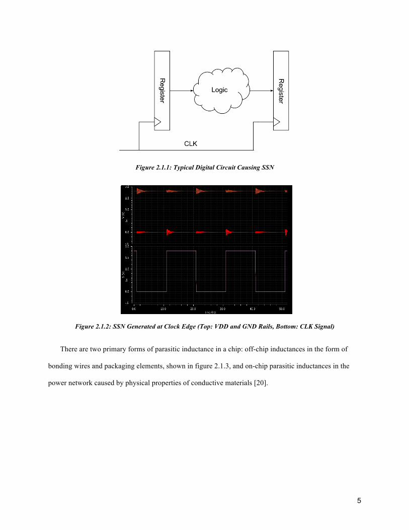
and with the magnitude of current change [19, 26]. Figure 2.1.1 shows the typical structure of digital
circuits that causes SSN, and figure 2.1.2 shows a simulation of SSN generated every clock tick.
5
Figure 2.1.1: Typical Digital Circuit Causing SSN
Figure 2.1.2: SSN Generated at Clock Edge (Top: VDD and GND Rails, Bottom: CLK Signal)
There are two primary forms of parasitic inductance in a chip: off-chip inductances in the form of
bonding wires and packaging elements, shown in figure 2.1.3, and on-chip parasitic inductances in the
power network caused by physical properties of conductive materials [20].

6
Figure 2.1.3: Off-Chip Bond Wire Inductances [19]
Three currents contribute to the switching noise of a CMOS circuit: short-circuit current, current
to/from the output node capacitance, and leakage current. Leakage current is small in magnitude and does
not change abruptly, so any contribution it makes to switching noise is dwarfed in comparison to the other
currents. Short-circuit current occurs when the input waveform switches states, and is caused by having a
conduction path from supply to ground while both the pull-up and pull-down networks are turned on,
illustrated as the green region in figure 2.1.4. The brief period of time in which both networks are on
occurs when the input voltage is between the threshold voltages of the NMOS and PMOS devices from
ground and supply, respectively.

7
Figure 2.1.4: CMOS Transition Diagram
The third source of current results from charging/discharging the output node capacitance. Large fan-
out gates or buses and I/O pins can contribute large node capacitances, which require more current to be
moved to/from the node. The combination of short-circuit current and output node charge storage
constitute the primary sources of system current variation in CMOS circuits that cause switching noise
when combined with parasitic inductances. Overall, SSN reduces the noise margin in digital circuits, and
can cause significant errors or complete circuit failure when analog circuits are interfaced with noisy
digital circuitry.
2.2 Traditional Approaches to Mixed Signal Chip Design
There are two common approaches to mixed signal system design regarding configuration of the
power network. The first is to simply connect all circuitry, both analog and digital, to one power and
ground for the system. While simple and efficient, this method means that any noise induced in the
digital circuitry shows up directly in the analog circuitry, so this method has largely been phased out.
More common is the method of isolation, which has an internal disconnect between the analog and digital

8
power and ground connections in the chip, that then requires connections to be made externally, since the
system must at some level reference the same power and ground for the analog and digital components to
be able to communicate. A popular approach to implementing isolation is to connect both the analog and
digital ground pins of a mixed signal IC to a large ground plane on the PCB. Ideally such a ground plane
spans an entire layer of the PCB, though in practice this is difficult to achieve. Large ground planes
reduce digital noise coupling to the analog circuitry [21]. For supply noise, an RC filter or ferrite bead
can be used to filter out the high frequency digital noise. While the power network isolation method does
reduce the noise induced on the analog power network, noise still leaks through via capacitive coupling.
In addition, the ground plane can take up a large percentage of the total PCB area.
A better solution than trying to isolate the digital and analog power networks is to use digital logic
that is lower noise than CMOS logic. MCML offers designers the opportunity to create digital circuits
that can share the same supply and ground as analog components, thereby eliminating the need for
sophisticated isolation networks. In addition, MCML gates run at higher speed and potentially lower
power than CMOS circuits, for only a marginal trade-off in chip area.
2.3 Reducing SSN via Constant Current Consumption in MCML
The key to reducing switching noise is limiting the rate of current change in some manor, assuming
parasitic inductances are fixed which is a fair assumption to make, as there is limited control over
reducing parasitics beyond a certain limit. CMOS circuits cause significant SSN because the current
through these devices is not limited or defined when they are switching states. When CMOS gates switch
they offer a very low resistance path – inducing large current spikes and ringing on the order of hundreds
of microamps to milliamps for large gates. MCML gates significantly reduce SSN because the current is
fixed via a biased tail current sink. MCML gates are not entirely immune to switching noise because of
channel length modulation. The tail current device of each MCML gate will have small VDS fluctuations
that occur when switching states, causing variations in system current on the order of a hundred

9
microamps for high drive strength MCML gates. However, simulations in the following section will
show that these changes are orders of magnitude lower than CMOS circuits.
Another advantage to MCML is that cells can be tailored to meet varying levels of system sensitivity
in mixed signal designs: SSN is controllable in an MCML circuit. This will be discussed in greater detail
in section 3.2.1.
2.4 Simulation Comparison of CMOS and MCML SSN in Presence of Parasitics
Simulators have difficulty representing real switching noise because typically the supply voltage is
provided by an ideal voltage source. Ideal voltage sources in SPICE have infinite drive strength and no
parasitic RLC components, meaning they can supply limitless current instantaneously without any voltage
fluctuation or ringing. In order to properly simulate SSN contributions of CMOS and MCML circuits,
parasitic RLC elements must be explicitly added between the ideal supply rail/ground and the local nodes.
For simulations, a lumped impedance model was used as shown in figure 2.4.1.
Figure 2.4.1: Lumped Impedance Model of Power Network Parasitics
In reality, the power network is made up of a huge number of RLC networks interconnected, but for
simplicity and ease of simulation, the lumped sum model is used. The lumped sum model takes into
account off-chip parasitics, such as pins and bond wires, as well as on-chip parasitics in the power
network [26].

10
Simulations in figures 2.4.2 – 2.4.9 show the SSN generated, as seen at the local supply and ground,
for CMOS and MCML gates using power network parasitics provided in [3] (shown in table 2.4.1) and
different number of gates switching. Figure 2.4.2 shows the input waveforms to the NAND gate,
indicating that all four input combinations were tested.
Table 2.4.1: Power Network Parasitics Tested
Parasitic R (Ω) Parasitic L (nH) Parasitic C (fF) 2 1 50 2 4 50 2 1 200 2 4 200 5 1 50 5 4 50 5 1 200 5 4 200
Figure 2.4.2: Input Signals for NAND Gate (CMOS Left, MCML Right)

11
2.4.1 1-Gate SSN Simulation Comparison
Figure 2.4.3: Local VDD and GND SSN; 5Ω, 1nH, 200fF (CMOS Left, MCML Right)
Figure 2.4.4: Local VDD and GND SSN; 5Ω, 1nH, 50fF (CMOS Left, MCML Right)

12
Figure 2.4.5: Local VDD and GND SSN; 2Ω, 4nH, 50fF (CMOS Left, MCML Right)
The worst-case result of these simulations is a 50mV variation for CMOS and 7mV for MCML. This
could be significant depending on the application, but should be manageable. However, the magnitude of
SSN increases dramatically when more gates are connected in parallel and switching together, effectively
simulating a higher activity factor and/or a larger CMOS circuit. Section 2.4.2 shows simulation results
for the same power network parasitics but with 10 gates switching in parallel for both CMOS and
MCML.
2.4.2 10-Gate SSN Simulation Comparison
Figure 2.4.6: Local VDD and GND SSN; 5Ω, 1nH, 200fF (CMOS Left, MCML Right)

13
Figure 2.4.7: Local VDD and GND SSN; 5Ω, 1nH, 50fF (CMOS Left, MCML Right)
Figure 2.4.8: Local VDD and GND SSN; 2Ω, 4nH, 50fF (CMOS Left, MCML Right)
The worst-case performance of the parallel 10-gate network is a 251mV deviation for CMOS and
24.5mV for MCML.
2.4.3 Large CMOS, Low-Noise MCML SSN Simulation Comparison
It turns out the simulations in sections 2.4.1 and 2.4.2 represent near best-case performance for
CMOS and mediocre performance for MCML in terms of the magnitude of SSN generated. A unique
feature of MCML gates is that they can be designed specifically to produce lower noise than illustrated
above. On the other hand, CMOS circuit noise performance only degrades as the devices are sized up.
Figure 2.4.9 shows the switching noise for the same 10-gate MCML NAND/AND configuration for a cell

14
tailored to very low noise specifications. Next to the MCML simulation is a 10-gate CMOS run with a 4x
NAND gate. The simulations were run for the worst-case parasitics.
Figure 2.4.9: Local VDD and GND SSN; 2Ω, 4nH, 50fF (4x CMOS Left, Low-Noise MCML Right)
For simplicity, it’s assumed the charge and discharge of the output node for a CMOS gate is a first
order RC network, with the resistance presented as the on-resistance of the transistor(s) and the
capacitance as the fan-out gate capacitance plus the parasitic transistor capacitances. Small RC time
constants are desirable for fast CMOS gates, however they increase the SSN because the rate at which
charge moves is directly proportional to the RC time constant. In addition, lower on-resistance allows
more short-circuit current to flow. Consequently, minimally sized CMOS gates have the lowest possible
SSN. Reducing the bias current and voltage swing of an MCML cell creates the opposite effect seen in
higher drive strength CMOS gates, reducing the SSN induced. Figure 2.4.9 shows a 2.2mV voltage
swing for the very low-noise MCML gate and 670mV swing for the 4x CMOS gate.
2.4.4 CMOS vs. MCML SSN Summary
The simulation results from the previous sections are summarized in figure 2.4.10. The raw data is
found in appendix A.

15
Figure 2.4.10: CMOS vs. MCML Power Network SSN Induced (Plotted in Ascending Order)
Figure 2.4.10 indicates that the MCML circuits exhibited a 10-fold decrease in SSN over the
equivalent CMOS circuits. In addition, MCML noise does not scale as drastically as CMOS, meaning
that CMOS noise has a tendency to runaway compared to MCML. This makes MCML a strong choice
for high performance mixed-signal chips. Most of the noise in CMOS circuits becomes common-mode
noise for MCML and is rejected by the differential stage [2]. For a given current, the difference between
the system and local VDD/GND (i.e. the magnitude of SSN) is determined by the equivalent impedance
of the lumped sum model, as given in equation 2.4.1. The worst-case performance for both MCML and
CMOS occurs for the largest inductive and smallest capacitive parasitics. Resistance increases the
settling time of the circuit. A more in-depth analysis of the effect of impedance components on SSN can
be found in appendix A.
𝑍!" =!!!"
!"#!!!!"!! (2.4.1)
The simulations support the positive correlation between switching noise and parasitic inductance,
and inverse relationship with parasitic capacitance. The results of the SSN simulations indicate it’s
possible to run analog and MCML digital circuitry from the same power and ground without requiring
any isolation whatsoever. This simplifies both the circuit level design of mixed-signal IC’s and also the
0
50
100
150
200
250
300
1 2 3 4 5 6 7 8
Power Network Noise (m
V)
Simulation
CMOS vs. MCML Power Network Noise Induced
MCML (1 Gate)
CMOS (1 Gate)
MCML (10 Gates)
CMOS (10 Gates)

16
system board level designs that make use of said IC’s. For the rest of this thesis, simulations comparing
CMOS to MCML that refer to the “best” case parasitics refer to 5Ω, 1nH, 200fF (i.e. lowest SSN), and
“worst” case refers to 2Ω, 4nH, 50fF (i.e. highest SSN).
2.5 Accurately Modeling System Parasitics
MOSIS specs the electrical characteristics of some of their package traces. Two sample packages are
shown in table 2.5.1 with the minimum parasitics for each package type.
Table 2.5.1: MOSIS Minimum Packaging Parasitics per Pin
Package (Pins) R (mΩ) L (nH) C (pF) Dual-inline package (28) 28.3 2.98 0.609 Pin-grid array (84) 89 2.95 1.43
Table 2.5.1 illustrates examples of off-chip parasitics, which must be added explicitly to the circuit
schematic or netlist. On-chip parasitics are modeled via extraction. Accurately predicting the parasitics
is a difficult process, though extraction attempts to model these parameters as accurately as possible by
analyzing the metal interconnects. There are three methods to model wires: lumped, distributed, and
transmission [26]. Lumped is simple but overly conservative, whereas distributed is more accurate but
complex. Both of these models assume inductance is negligible and only account for resistive and
capacitive components. When parasitic inductances start to dominate in high-speed devices, a
transmission line model must be used which adds inductance to the distributed model.

17
CHAPTER 3
MCML Gate Topology and Design Optimizations
Designing MCML gates is difficult because of the inherent asymmetry of the gates and number of
circuit parameters available to modify. In addition, routing MCML circuits is more difficult because
MCML runs off differential logic, requiring twice the number of connections to be routed compared to
CMOS. CMOS based designs have standard rules of thumb that exist to optimize transistor sizes based
on design goals and gate symmetry. For example, if a sharp rising edge is desired for a rising edge
triggered flip-flop, the PMOS pull-ups can be sized up to drive signals high faster. If the goal is equal
rise and fall times, the transistors can be sized such that carrier mobility differences are offset by the
PMOS to NMOS size ratios. Transistor sizes are the only controllable circuit parameter in CMOS design.
MCML gates have two primary performance metrics: voltage swing and bias current. These two
quantities dictate the gate performance with respect to common digital performance metrics such as:
noise, speed, power, and noise margin, and are controlled via the transistor W/L ratios and bias voltages.
This chapter establishes relationships between the primary metrics and common digital metrics, as well as
additional metrics specific to MCML circuit design. Once these relationships are understood, they serve
as a baseline to speed-up the process of developing additional MCML gates and optimizing gates for a
given specification or application.
3.1 Generic MCML Gate Description and MCML Inverter/Buffer Functionality
At a high level, MCML gates consist of a differential input stage (pull-down network) of NMOS
devices that implements the cell logic, pull-up active load PMOS network, and biased tail NMOS current
source. The general design of an MCML gate is shown in figure 3.1.1.

18
Figure 3.1.1: Generic MCML Gate [3]
The simplest MCML gate is the inverter/buffer shown in figure 3.1.2. The operation is as follows:
input high turns on the NMOS “IN” transistor, steering the bias current through the left “INV” branch.
The “INV” branch must discharge down to the voltage set by the pull-up device, while the right “BUF”
branch is charging as the NMOS “!IN” transistor turns off, causing the right side to pull-up to VDD. The
logic high voltage therefore is VDD for MCML gates. When the input is logic low, the current is steered
to the right and the outputs toggles.

19
Figure 3.1.2: MCML Inverter/Buffer Gate
MCML gate parameters control the voltage swing and bias current of the gate, and therefore
indirectly dictate the gates performance in terms of noise generation, speed, power consumption, area,
noise margin (robustness), and more. These designer controllable parameters are summarized in table
3.1.1.
Table 3.1.1: MCML Gate Design Parameters
Device Modifiable Parameters
PMOS pull-up Width, length, RFP voltage
NMOS pull-down Width, length
NMOS tail current Width, length, RFN voltage
In addition to the shear number of parameters available to modify, not many well-defined rules exist
for MCML as to how these parameters affect the different digital performance metrics. Understanding
what parameters we have control over is the first step towards designing an MCML cell, the second is

20
how the circuit parameters affect the performance metrics. In MCML, the logic (voltage) swing and bias
current are completely controllable by the designer, and are the two functional parameters that affect all
metrics. To understand exactly how the parameters in table 3.1.1 affect the performance metrics, each
distinct portion of an MCML inverter/buffer cell is dissected, starting the discussion from the top down.
For the simulations characterizing MCML gate performance in sections 3.1.1 – 3.1.4, the resulting trends
are far more important than the numerical results, as the gate tested was a single implementation of an
MCML inverter/buffer. In addition, the gate was driven using near-ideal waveforms and unloaded
outputs to simplify the simulation methodology.
3.1.1 PMOS Pull-Up Device Function, Sizing and Performance Tradeoffs
The pull-up devices serve as an active load, and are biased in the linear region to pull the “off” side of
the inverter/buffer cell up to VDD and to drive the “on” side to the logic low voltage. For a given bias
current (ISD), RFP (VSG) voltage, and transistor dimension, the voltage drop (VSD) across the pull-up
device follows the PMOS current equation in the linear region, as given in equation 3.1.1 and solved for
VSD in equation 3.1.2. MCML gates have a logic low voltage of VDD minus the PMOS voltage drop,
VSD, controlled by the W/L ratio and RFP voltage of the pull-up devices. The cells in this thesis have the
RFP voltage fixed at 0V (i.e. tied to ground) for all gates. This drives the pull-up devices deep into the
linear region and also simplifies the design of the MCML circuits by requiring less biasing circuitry and
fewer signals to route. The disadvantage is that the RFP voltage does not affect the cell area, while
changing the W/L ratio does.
𝐼!" = 𝜇!𝐶!"!!
𝑉!" − 𝑉!" 𝑉!" −!!"!
!1 + 𝜆𝑉!" (3.1.1)
𝑉!" = 𝑉!" − 𝑉!" − 𝑉!" − 𝑉!"! − 2 !
!!!"!!!!"
(3.1.2)
The pull-up W/L ratio exhibits an inverse square relationship to the voltage swing (eq. 3.1.2) –
increasing the W/L ratio reduces the voltage swing of the cell. Figure 3.1.3 shows the results of
21
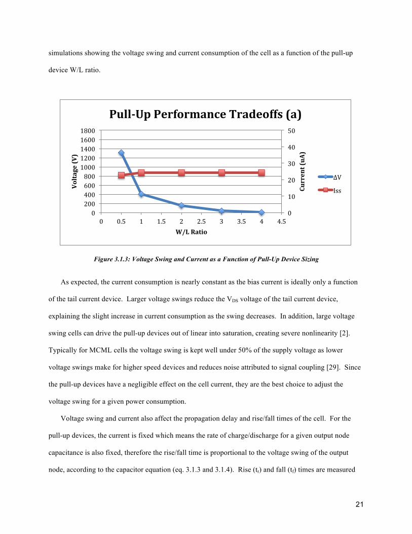
simulations showing the voltage swing and current consumption of the cell as a function of the pull-up
device W/L ratio.
Figure 3.1.3: Voltage Swing and Current as a Function of Pull-Up Device Sizing
As expected, the current consumption is nearly constant as the bias current is ideally only a function
of the tail current device. Larger voltage swings reduce the VDS voltage of the tail current device,
explaining the slight increase in current consumption as the swing decreases. In addition, large voltage
swing cells can drive the pull-up devices out of linear into saturation, creating severe nonlinearity [2].
Typically for MCML cells the voltage swing is kept well under 50% of the supply voltage as lower
voltage swings make for higher speed devices and reduces noise attributed to signal coupling [29]. Since
the pull-up devices have a negligible effect on the cell current, they are the best choice to adjust the
voltage swing for a given power consumption.
Voltage swing and current also affect the propagation delay and rise/fall times of the cell. For the
pull-up devices, the current is fixed which means the rate of charge/discharge for a given output node
capacitance is also fixed, therefore the rise/fall time is proportional to the voltage swing of the output
node, according to the capacitor equation (eq. 3.1.3 and 3.1.4). Rise (tr) and fall (tf) times are measured
0
10
20
30
40
50
0 200 400 600 800 1000 1200 1400 1600 1800
0 0.5 1 1.5 2 2.5 3 3.5 4 4.5
Current (uA)
Voltage (V)
W/L Ratio
Pull-‐Up Performance Tradeoffs (a)
ΔV
Iss

22
10%-90% of the voltage swing and are presented on different vertical axis due to the potential for large
discrepancies between the two measurements, discussed in greater detail in section 3.3.2. Propagation
(prop) delay (tpd) is 50% input swing to 50% output swing and is the average of the high and low prop
delays.
𝐼! = 𝐶 !!!!"
(3.1.3)
𝑑𝑡 = !!"!!!
(3.1.4)
Simulation results for prop delay and rise/fall time as a function of pull-up W/L ratio are shown in
figure 3.1.4.
Figure 3.1.4: Prop Delay and Rise/Fall Time as a Function of Pull-Up Device Sizing
The rise, fall, and prop delay curves closely resemble the voltage swing curve (fig. 3.1.3) as expected,
since gate speed decreases as voltage swing increases assuming a fixed current. The large fall time for a
W/L ratio of 0.5 is the result of the voltage swing setting the pull-up devices near their VDSsat voltage,
around 1400mV swing for the gate tested. At this point the devices exhibit extreme non-linearity, which
causes the fall time to increase significantly. For low noise and high-speed applications, low swing
MCML gates should be used.
0 100 200 300 400 500 600 700 800
0
20
40
60
80
100
120
0 0.5 1 1.5 2 2.5 3 3.5 4 4.5
Fall Time (ps)
Prop/Rise Time (ps)
W/L Ratio
Pull-‐Up Performance Tradeoffs (b)
Rise
Prop
Fall

23
3.1.2 NMOS Pull-Down Device Function, Sizing and Performance Tradeoffs
The pull-down devices implement the logic for the MCML gate based on their configuration. In the
case of the inverter/buffer, a single pair of pull-down devices is sufficient. It’s fundamental to MCML
cells that each pull-down device have a complementary device with the opposite polarity differential as
the input.
The only modifiable parameter for the pull-down devices is the W/L ratio. Considering that the pull-
up network fixes the voltage swing and the tail current device fixes the current, the pull-down devices are
modeled as switches and therefore should not play a role in the cell performance. Simulations looking at
the effects of changing the W/L ratio of the pull-down devices on voltage swing and power consumption
are shown in figure 3.1.5, and on prop delay and rise/fall times in figure 3.1.6.
Figure 3.1.5: Voltage Swing and Current as a Function of Pull-Down Device Sizing
Figure 3.1.5 shows that the pull-down network has a negligible impact on the voltage swing and
current consumption of the MCML gate.
0
10
20
30
40
50
0 200 400 600 800 1000 1200 1400 1600 1800
0 2 4 6 8 10 12 14 16 18
Current (uA)
Voltage (V)
W/L Ratio
Pull-‐Down Performance Tradeoffs (a)
ΔV
Iss

24
Figure 3.1.6: Prop Delay and Rise/Fall Time as a Function of Pull-Down Device Sizing
Figure 3.1.6 shows a linear correlation between pull-down device W/L ratio and gate delay. This is
due to the increase in capacitance from a larger transistor. In general the pull-down devices should be
near minimum sized to reduce area and delay, however there is an incentive to increase the W/L ratio
discussed in section 3.3.4.
3.1.3 Tail Current Device Function, Sizing and Performance Tradeoffs
The tail current device is operated in the saturation region as a constant current source with a fixed
RFN (VGS) voltage. Equation 3.1.5 describes the ideal current through this device.
𝐼!" =!!𝜇!𝐶!"
!!𝑉!" − 𝑉!" !(1 + 𝜆𝑉!") (3.1.5)
The W/L ratio and VGS are both controllable parameters for the tail current device – increasing either
will increase the bias current for the gate. Also recall that the voltage swing for the cell increases with
increased IDS (eq. 3.1.2) for the pull-up devices. Similar to the pull-up devices, large voltage swing
reduces the VDS voltage of the tail current device and forces the device closer to the linear region.
Simulations showing the voltage swing and current as a function of tail current device size are shown in
figure 3.1.7.
0 20 40 60 80 100 120 140 160
0 2 4 6 8 10 12 14 16 18
Time (ps)
W/L Ratio
Pull-‐Down Performance Tradeoffs (b)
Rise
Prop
Fall

25
Figure 3.1.7: Voltage Swing and Current as a Function of Tail Current Device Sizing
Figure 3.1.7 shows that increasing the W/L ratio of the tail current device increases current
consumption (eq. 3.1.5) and voltage swing, dictated by the pull-up devices (eq. 3.1.2). Channel length
modulation adds an extra order to the ideal MOSFET current equation, and explains the slight non-
linearity in the current curve. After a W/L ratio of 2, the voltage swing is large enough that the pull-up
devices are forced into saturation and the tail current device is pushed into linear, at which point the pull-
ups limit the current causing the curve to level off. The tail current device must reside in saturation and
the pull-up devices must reside in linear for an MCML gate to function properly. The defining equations
for an NMOS device to be in saturation and a PMOS device to be in linear are given in equations 3.1.6
and 3.1.7, respectively. The VDSsat voltages of the tail current and pull-up devices determine the upper-
limit on voltage swing; the derived results are given in equations 3.1.8 and 3.1.9.
𝑉!" > 𝑉!" − 𝑉!" 𝑎𝑛𝑑 𝑉!" > 𝑉!" (3.1.6)
𝑉!" < 𝑉!" − 𝑉!" 𝑎𝑛𝑑 𝑉!" > |𝑉!"| (3.1.7)
Δ𝑉 < 𝑉!! − 𝑉!" !"#$ !"#$ − 𝑉!! (3.1.8)
Δ𝑉 < 𝑉!" !"##!!" !"#$ − |𝑉!"| (3.1.9)
0
10
20
30
40
50
0 200 400 600 800 1000 1200 1400 1600 1800
0 1 2 3 4 5 6 7 8 9
Current (uA)
Voltage (V)
W/L Ratio
Tail Device Performance Tradeoffs (a)
ΔV
Iss

26
The take-away from figure 3.1.7 is that the tail current device W/L ratio has a significant impact on
the voltage swing and power consumption for any MCML cell. Tail current devices should always be
non-minimum length to increase output impedance and reduce transistor mismatch. In addition, larger
W/L ratios decrease the VDSsat voltage and create the potential for lowering VDD [2].
Additional simulations showing the relationship between prop delay, rise, and fall time with respect
to tail current device W/L ratio are shown in figure 3.1.8.
Figure 3.1.8: Prop Delay and Rise/Fall Time as a Function of Tail Current Device Sizing
In section 3.1.1 it was shown that the rise/fall time and prop delay increase proportionally to the
voltage swing for a fixed current. Figure 3.1.8 shows that an increase in current consumption roughly
offsets the increase in voltage swing, creating a nearly constant rise time and prop delay. The spike in the
fall time occurs when the pull-ups sit near their VDSsat voltage, as discussed before.
The other parameter affecting the tail current device performance is the bias RFN (VGS) voltage.
Simulations showing the voltage swing, current consumption, prop delay, and rise/fall time as a function
of RFN voltage are shown in figures 3.1.9 and 3.1.10.
0
50
100
150
200
250
300
350
0
20
40
60
80
100
120
0 1 2 3 4 5 6 7 8 9 Fall Time (ps)
Prop/Rise Time (ps)
W/L Ratio
Tail Device Performance Tradeoffs (b)
Rise
Prop
Fall

27
3.1.4 RFN Voltage Performance Tradeoffs
Figure 3.1.9: Output Voltage Swing and Current versus RFN Voltage
As expected, the current rises exponentially with RFN up to 1.0V (eq. 3.1.5), at which point the pull-
up devices reside in saturation and limit the current and voltage swing.
Figure 3.1.10: Prop Delay and Rise/Fall Time as a Function of RFN Voltage
0
10
20
30
40
50
0 200 400 600 800 1000 1200 1400 1600 1800
0 0.2 0.4 0.6 0.8 1 1.2 1.4 1.6 1.8 2
Current (uA)
Voltage (V)
RFN (V)
RFN Performance Tradeoffs (a)
ΔV
Iss
0
50
100
150
200
250
300
350
0
20
40
60
80
100
120
0 0.2 0.4 0.6 0.8 1 1.2 1.4 1.6 1.8 2
Fall Time (ps)
Prop/Rise Time (ps)
RFN (V)
RFN Performance Tradeoffs (b)
Rise
Prop
Fall

28
Figure 3.1.10 shows the rise/fall time and prop delay for RFN voltages that produce measureable
voltage swings. Again, the voltage swing and current offset each other with respect to rise time and prop
delay, and the fall time exhibits a non-linear region near 1400mV swing.
An important practical consideration when designing an MCML cell is to know the useful and
attainable regions of the RFN voltage. The useful region for the simulations in figure 3.1.9 would be for
RFN voltages between 0.6 to 1.0V. Below 0.6V the cell has no voltage swing and therefore is not a
functional MCML cell. Above 1.0V the gate is no longer biased properly, making the cell inefficient.
The attainable region corresponds to the RFN voltages that are possible to achieve using a biasing circuit.
Most biasing circuits cannot achieve voltages near ground or supply, so this must be taken into
consideration when designing and testing any MCML cell, and will be discussed in greater detail in
section 3.2.6.
The RFN voltage should be the first parameter examined when looking to modify the performance of
an MCML cell. Unlike modifying transistor sizes, which requires an entirely new layout for each MCML
cell, the RFN voltage only needs a new biasing circuit. In addition, the RFN voltage does not increase the
transistor size.
3.2 Power Consumption Impact on MCML Gate Performance
Power consumption for any MCML gate is theoretically well defined, as given in equation 3.2.1. ISS
is the bias current sunk by the tail current device and VDD is the supply voltage. In addition to setting the
power consumption, voltage swing, and speed, the bias current is an important parameter when designing
MCML gates because it has a strong correlation to noise generation, as will be discussed in the following
section.
𝑃!"!# = 𝑉!!𝐼!! (3.2.1)
For comparison, CMOS gate power is given in equation 3.2.2. The main difference between CMOS
and MCML power consumption is that CMOS power scales with operating frequency. This makes

29
MCML a more power efficient topology at higher operating frequencies, though that is not the focus of
this thesis.
𝑃!"#$ =∝ 𝑉!!!𝐶𝑓 (3.2.2)
3.2.1 Very Low Noise MCML Design
Noise generation in digital circuits is tied directly to the ability of the circuit to limit the rate of
current change through the parasitic inductances. CMOS gates switch from leakage level current to large,
momentary current spikes when switching states, while MCML gates have an ideally constant bias
current (i.e. no current change). MCML cells conducting less current reduce the magnitude of current
change, which decreases SSN (eq. 2.1.1). In addition, lower voltage swing requires less charge
movement to charge and discharge the output node and also reduces the fluctuation in the VDS voltage of
the tail current device that causes channel length modulation. Consider a theoretical MCML gate that
could operate with a 0mV swing – the gate would instantaneously switch states and would effectively
operate at steady state, i.e. no current change and no SSN. Providing digital designers control over the
switching noise introduced to the power network in mixed-signal chips allows them to meet stringent
analog noise requirements while still being able to optimize the performance of the digital circuitry.
Compared to CMOS, MCML gates have relatively low noise margins, and reducing the voltage swing
further makes the gate more prone to logic errors. However, MCML gates compensate for lower noise
margin by producing less noise than equivalent CMOS gates. Figure 2.4.9 in section 2.4.3 is an example
of an MCML gate designed specifically for low current consumption to reduce the SSN to under 3mV.
3.2.2 High Speed MCML Gates and Driving Large Capacitive Loads
While low current MCML gates reduce SSN, they also produce slower gates. For any real MCML
cell the current switching is not instantaneous and the rate at which the output nodes are
charged/discharged is dependent on the output node capacitance, bias current, and the voltage swing (eq.

30
3.1.4). High drive strength MCML gates refer to gates with large bias current and low voltage swing.
High-speed MCML circuits require high drive strength gates and small transistors to reduce the parasitic
capacitances. In order to model an accurate load, a matching network was setup to determine the input
capacitance for the MCML inverter/buffer, as shown in figure 3.2.1. The matching network uses two
buffers to ensure the signal applied to the unit under test (UUT) is a reasonable representation of a true
signal as opposed to an ideally driven input.
Figure 3.2.1: Matching Network to Determine MCML Inverter/Buffer Input Capacitance
Simulation results indicate that the input capacitance was roughly 1fF. Figures 3.2.2 and 3.2.3 show
simulations for an MCML inverter/buffer driving a 1fF (single gate), 4fF (fan-out 4), and 10fF (large)
load for a given voltage swing and bias current.

31
Figure 3.2.2: Prop Delay vs. Voltage Swing for Given Load Capacitance
Figure 3.2.2 proves that voltage swing exhibits a linear relationship to prop delay for a given load
capacitance and current (eq. 3.1.4), therefore reducing the voltage swing creates a proportionally faster
gate. For these simulations the current was fixed at 23.9µA and the voltage swing was modified.
0
50
100
150
200
250
300
0 100 200 300 400 500 600 700 800 900
Prop Delay (ps)
Voltage Swing (mV)
Prop Delay vs. Voltage Swing for Different Load Capacitances
1fF
4fF
10fF

32
Figure 3.2.3: Prop Delay vs. Bias Current for Given Load Capacitance
Figure 3.2.3 verifies the inverse relationship between current and prop delay for a given load and
voltage swing (eq. 3.1.4). For these simulations the voltage swing was fixed at 400mV and the current
was modified. The important point illustrated by figure 3.2.3 is that low power MCML gates come at a
tremendous cost in speed. Low power MCML gates require small voltage swings to offset the speed lost
from reducing the bias current. Despite creating a less robust gate, low swing and low power gates
produce less SSN and therefore a more stable environment.
In general, these simulations indicate that MCML gate speed increases with current consumption and
decreases with voltage swing, and there exists a direct trade-off between noise, speed, and power
consumption that must be considered by the designer.
Driving large capacitive loads requires high drive strength MCML gates, or alternatively, multiple
lower drive gates connected in parallel achieve the same result at the cost of reduced area efficiency.
Very large loads require a large bias current because the voltage swing has a lower limit for a robust gate.
0 200 400 600 800 1000 1200 1400
0 20 40 60 80 100
Prop Delay, tpd (ps)
Current, Iss (uA)
Prop Delay vs. Bias Current for Different Load Capacitances
1fF
4fF
10fF

33
3.2.3 Current Matching Ratio (CMR)
Current matching ratio (CMR) measures how close the tail current device current (ISS) matches the
current mirror bias current (Iref), as given in equation 3.2.3. CMR must be unity for the ideal power
equation to hold (eq. 3.2.1), meaning ISS and Iref must be equal for all gates. Process variation, output
impedance, and supply voltage all play a role in determining the CMR.
𝐶𝑀𝑅 = !!!!!"#
(3.2.3)
𝑉!" = 𝑉!" − 𝑉!" (3.2.4)
Process variation causes threshold voltage and transistor dimension differences compared to nominal
performance. Increasing the overdrive voltage, defined in equation 3.2.4, reduces error due to threshold
voltage offset. Non-minimum channel length devices should be used for all tail current and biasing
devices to increase output impedance and reduce sensitivity to channel length modulation. Non-minimum
sized devices also improve transistor matching; fabricated channel lengths have absolute tolerances,
meaning larger devices will have less error as a percentage of the total W/L ratio and therefore better
matching [28]. Process corner analysis, a method to check worst-case circuit performance discussed in
greater detail in section 3.3.5, was run to measure the potential error in CMR against the nominal size of
the tail devices width and length dimension. The simulation results are presented in figure 3.2.3.

34
Figure 3.2.4: Four-Corner Analysis for CMR vs. Tail Device Width and Length Dimensions
Figure 3.2.4 shows that CMR exhibits a decaying exponential relationship to tail device W/L
dimensions. An absolute minimum channel length of 720nm (four times minimum) was set for the tail
current devices to ensure good matching but allow for reasonable sized devices. The other take-away is
that the CMR is typically always above unity due to larger VDS voltage across the gate tail current device
compared to the biasing circuit.
Supply voltage also has a direct impact on the output of current mirrors, but since MCML is a low
noise family the supply should not fluctuate enough to cause significant miscalculations [2].
3.2.4 MCML System Level Power Consumption
Power for an entire MCML circuit can be calculated as per equation 3.2.5.
𝑃!"#!$"% = 𝑉!! ∗ 𝑁! + 𝐵𝑛! ∗ 𝐼𝑠𝑠!!!!! (3.2.5)
The system power equation accounts for the likelihood of multiple biasing circuits to drive different
strength MCML gates, and assumes a CMR of unity. For each bias voltage (d) in the circuit, there will be
1 1.01 1.02 1.03 1.04 1.05 1.06 1.07 1.08 1.09 1.1
100 2100 4100 6100 8100 10100 12100
CMR
Tail Devices W, L Dimension (nm)
Process Corners Analysis for CMR vs. Tail Current W, L Dimension
tt
fs
sf
ff
ss

35
some number of MCML gates (Nd) connected to some number of biasing circuits (Bnd). Ideally only one
biasing circuit is needed for each bias voltage generated, as shown in figure 3.2.5, but it may be necessary
in large circuits to have local distributions of bias voltages requiring more than one biasing circuit for a
given bias voltage. The sum of MCML gates and biasing circuits multiplied by the bias current (Issd)
gives the total current consumed for that bias voltage. The system power is then the sum of all bias
voltage currents multiplied by the supply voltage (VDD). For back of the envelope calculations, it’s
sufficient to drop Bnd because Nd typically dominates by at least an order of magnitude.
Figure 3.2.5: Arbitrary MCML Circuit with Single Biasing Circuit
3.2.5 Selection of Biasing Circuitry
To implement an MCML circuit, there must be at least one biasing circuitry for each bias voltage
required by the MCML cells. Core logic can typically operate on two bias voltages, one for all
combinational cells, and one for DETFF’s, which require a larger bias current for the same voltage swing.
I/O pins and large buses may require even higher drive strength cells that need additional bias voltages.
When developing and testing MCML cells it’s common to generate an ideal RFN voltage for simulations
and testing, but the end product must have actual circuits that can implement the desired bias voltage(s).

36
A basic active load bias circuit, one of the simplest current mirror topologies, was simulated to
identify the attainable voltage range for the given topology. The schematic is shown in figure 3.2.6, and
the simulation results in figures 3.2.7 and 3.2.8.
Figure 3.2.6: Basic Active Load Current Mirror
Figure 3.2.7: RFN Voltage and Bias Current as a Function of PMOS Active Load W/L Ratio
0
50
100
150
200
0 200 400 600 800 1000 1200 1400 1600 1800
0 5 10 15 20 25 30
Current (uA)
Voltage (V)
W/L Ratio
Bias Voltage and Current vs. PMOS W/L Ratio
RFN
Iss

37
Figure 3.2.8: RFN Voltage and Bias Current as a Function of NMOS W/L Ratio
Figures 3.2.7 and 3.2.8 show the RFN voltage (blue) and reference current (red) as a function of the
PMOS and NMOS W/L ratio, respectively. The results indicate that a voltage ranging from about 0.4V to
1.7V is attainable. However, the size of the devices begins to grow out of control for the lowest and
highest voltages. Assuming the PMOS and NMOS devices are sized with non-minimum lengths of
720nm for better CMR, the widths must be at least 18µm to get 0.4V or 1.7V. There are tradeoffs for the
biasing circuitry – large bias circuits that create either large or small RFN voltages offer the potential to
reduce the sizes of the MCML gate tail current devices to achieve a desired gate current. Since MCML
gates in any circuit outnumber biasing circuits by at least an order of magnitude, it may be overall more
area efficient to use low or high RFN voltages. If possible, setting the RFN voltage for MCML gates near
0.8V allows for small biasing circuits, so this was the goal for standard cells designed in this thesis.
Implementing dynamic RFN voltage adjustments to reduce power consumption could be done in one
of two ways: discrete RFN bias circuits or feedback based circuits. Discrete biasing would require some
control logic to switch between RFN voltages as desired, with a different bias circuit for each RFN.
Analog feedback can implement a circuit in which the output voltage has a negative correlation to
temperature using MOSFET temperature coefficients.
0
50
100
150
0 200 400 600 800 1000 1200 1400 1600 1800
0 5 10 15 20 25 30
Current (uA)
Voltage (V)
W/L Ratio
Bias Voltage and Current vs. NMOS W/L Ratio
RFN
Iss

38
3.3 MCML Gate Robustness and Process Variation
Reliable gate performance is an important metric when designing digital circuits. Robustness, or
noise margin, is most directly related to the voltage swing of the gate, and is indicative of how immune
the gate is to changes in VDD, noise, and transistor mismatch.
3.3.1 Voltage Swing Ratio (VSR)
Voltage swing ratio (VSR) is a measure of how close the differential output voltage swing is to the
differential input voltage swing, as defined in equation 3.3.1. Unity is best, however non-ideal current
switching can cause degradation in VSR. An ideal MCML gate steers all bias current down one branch of
the circuit, leaving the other branch no current and therefore no voltage drop across the pull-up transistor
(eq. 3.1.2). This yields a high voltage of VDD and low voltage set by the bias current and pull-up device.
Real MCML gates are not able to completely switch off the pull-up branch, leaving a finite amount of
current flowing through the “off” path that causes an effective IR drop across the pull-up devices and
reduces the high voltage and causes a rise in the low voltage in the “on” path. Current switching is
improved by use of larger input voltage differentials, pull-up W/L ratios, and bias current [2]. If possible,
it’s better to use larger pull-up W/L ratios to improve VSR, which allows for lower voltage swing and
bias current to minimize SSN.
𝑉𝑆𝑅 = ∆!!"#∆!!"
(3.3.1)
3.3.2 Rise-Fall Ratio (RFR)
Rise-fall ratio (RFR) quantifies the relationship between the rise and fall time of an MCML gate, and
is given in equation 3.3.2. As seen in section 3.1.1, it’s possible to have MCML gates with very large fall
times for one differential output and comparatively short rise time for the other. The fall time issue is the
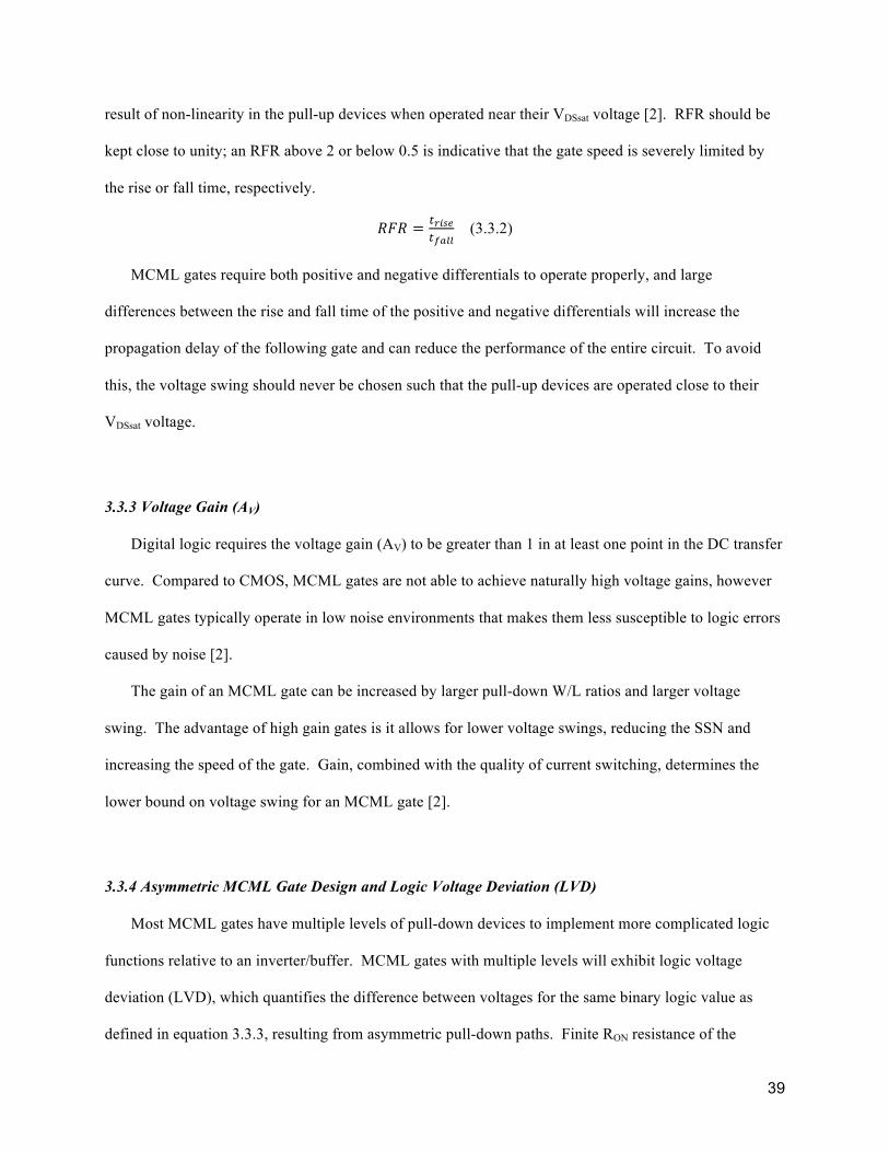
39
result of non-linearity in the pull-up devices when operated near their VDSsat voltage [2]. RFR should be
kept close to unity; an RFR above 2 or below 0.5 is indicative that the gate speed is severely limited by
the rise or fall time, respectively.
𝑅𝐹𝑅 = !!"#!!!!""
(3.3.2)
MCML gates require both positive and negative differentials to operate properly, and large
differences between the rise and fall time of the positive and negative differentials will increase the
propagation delay of the following gate and can reduce the performance of the entire circuit. To avoid
this, the voltage swing should never be chosen such that the pull-up devices are operated close to their
VDSsat voltage.
3.3.3 Voltage Gain (AV)
Digital logic requires the voltage gain (AV) to be greater than 1 in at least one point in the DC transfer
curve. Compared to CMOS, MCML gates are not able to achieve naturally high voltage gains, however
MCML gates typically operate in low noise environments that makes them less susceptible to logic errors
caused by noise [2].
The gain of an MCML gate can be increased by larger pull-down W/L ratios and larger voltage
swing. The advantage of high gain gates is it allows for lower voltage swings, reducing the SSN and
increasing the speed of the gate. Gain, combined with the quality of current switching, determines the
lower bound on voltage swing for an MCML gate [2].
3.3.4 Asymmetric MCML Gate Design and Logic Voltage Deviation (LVD)
Most MCML gates have multiple levels of pull-down devices to implement more complicated logic
functions relative to an inverter/buffer. MCML gates with multiple levels will exhibit logic voltage
deviation (LVD), which quantifies the difference between voltages for the same binary logic value as
defined in equation 3.3.3, resulting from asymmetric pull-down paths. Finite RON resistance of the

40
MOSFET devices causes a small voltage drop VDS across each device. This means the path with fewer
transistors will have a slightly lower logic low voltage compared to the longer path. Larger voltage gain
MCML cells exhibit less LVD. For a minimum length NMOS device, the LVD for an MCML
NAND/AND gate as a function of pull-down W/L ratio is shown in figure 3.3.1.
𝐿𝑉𝐷 = 𝑉!"#(!"#) − 𝑉!"#(!"#) (3.3.3)
Figure 3.3.1: MCML NAND/AND Logic Voltage Deviation vs. Pull-Down Device W/L Ratio
Figure 3.3.1 indicates that for an MCML NAND/AND gate the worst-case LVD is 11.9mV. This is
relatively insignificant for gates with a voltage swing on the order of hundreds of millivolts, but a high
speed MCML gate attempting to implement sub-hundred millivolt logic swing may be prone to LVD that
could cause a logic error. In addition, LVD scales with the number of logic levels implemented. The
trade-off to reducing ripple voltage is increased device area and lower gate speed as a result of larger
transistors (fig. 3.1.6). It was determined that pull-down devices with a W/L ratio of 4 offered a
reasonable reduction in LVD with minimal effect on silicon area and gate speed for a given gate.
Another solution to reduce LVD is to add pull-down device(s) in the shorter transistor path(s) with
the gate(s) tied to VDD, effectively matching all path “on” resistances. This may be a better solution for
high-speed applications.
0
2
4
6
8
10
12
14
0 2 4 6 8 10 12 14 16 18
LVD (m
V)
W/L Ratio
LVD vs. Pull-‐Down W/L Ratio

41
3.3.5 Process Corners Analysis
Process corners is an analysis method that models process variation by using information provided by
the foundry to provide worst-case behavior of a circuit [32]. The corners method used here bases the
results on “fast” (f) and “slow” (s) devices. The first letter indicates the relative speed of the NMOS
devices, and the second of the PMOS devices. Typical performance is indicated by “tt”. Process corners
was run on the MCML inverter/buffer to verify that the design would still perform functionality in the
extreme cases and to quantify the potential variation in performance. The simulation results showing the
effect on current consumption and voltage swing are shown in figure 3.3.2, and the result on gate speed in
figure 3.3.3.
Figure 3.3.2: Process Corner Analysis for Voltage Swing and Current Consumption
Figure 3.3.2 indicates that the voltage swing can decrease 28% and power consumption can increase
30% compared to nominal performance. The minimum voltage swing is large enough to always drive the
next gate, so this is an acceptable result. The power consumption could be concerning in larger circuits if
not budgeted for, so this should be taken into account.
0
5
10
15
20
25
30
35
0
100
200
300
400
500
600
700
tt sf fs ss ff
Current (uA)
Voltage Swing (mV)
Process Corner Analyis (a) for Voltage Swing and Current
∆V
Iss

42
Figure 3.3.3: Process Corner Analysis for Rise/Fall Time and Propagation Delay
Figure 3.3.3 shows that prop delay and rise time are relatively consistent, however the fall time can
increase by more than 36%, which could potentially reduce the speed of the next gate. If the results of the
corners analysis are not adequate for given performance specification, there are ways to help mitigate
process variation that can be used to yield more consistent performance across the corners spectrum.
These techniques will be discussed in the following section.
3.3.6 Mitigating Process Variation through Quality Design and Layout Practices
Process variation causes differences in fabricated device threshold voltages, transistor dimensions,
and oxide thickness, among others. Process variation is a challenge to all designers designing at the
silicon level, but is typically not a major concern for CMOS designs. MCML gates are more sensitive to
this phenomenon as it can cause an underestimation of system power consumption and loss of speed.
Process variation causes transistor mismatch resulting from deviations in fabricated channel dimensions
due to printer accuracy, as well as spatial variations that result in slightly different doping densities and
well depths that lead to threshold voltage differences. Process variation exhibits an absolute error margin;
on the design side, non-minimum dimensions and large voltages reduce the effects of transistor mismatch.
0 10 20 30 40 50 60 70 80 90 100
tt sf fs ss ff
Time (ps)
Process Corner Analyis (b) for Rise/Fall Time and Prop Delay
tpd
tf
tr

43
On the layout side, there are a variety of ways to improve matching, with the cost being lower area
efficiency. Consider the progression of layout options for a set of differential pair transistors shown in
figures 3.3.4 – 3.3.7.
Figure 3.3.4: No Sharing; Moderate Matching, Moderate Area Efficiency [31]
Figure 3.3.5: Shared Source; Poor Matching, Best Area Efficiency [31]
Figure 3.3.6: Common Centroid; Best Matching, Lowest Area Efficiency [31]
Figure 3.3.7: Common Centroid, Shared Source; Good Matching, Low Area Efficiency [31]
Common centroid is a well-known technique that adjusts for gradients in both the X and Y direction.
Common centroid involves splitting transistors into fingers and orienting the fingers in such a way as to
match the distance from the center point in both directions, as shown in figures 3.3.6 and 3.3.7. Standard
cell transistors are typically minimally sized or close to it, and the 7RF process restricts the width of a
finger to 220nm. In addition, utilizing common centroid is the least area efficient method of transistor

44
layout. For the standard cells in this library, common centroid was determined to be too inefficient to
employ, but for additions of more cells to this library it could be an effective strategy to mitigate
variation. Appendix B provides more detailed analysis of process variation using process corners
analysis.
Another layout practice that should be employed for optimal MCML routing is running differential
signals as close to each other as possible. Any noise or cross-talk affecting one differential should affect
the other one when the pair is routed together, which will then become common mode and be rejected by
the next gate.
3.4 Expanding MCML Gate Design
Once the underlying relationships between MCML gate performance metrics and operating principles
of the pull-up, pull-down, and tail current devices are understood, more gates can be developed. The
process of designing more complicated gates involves stacking differential NMOS pull-down devices to
achieve the desired logic.
3.4.1 Developing More Complicated MCML Gates
NAND gates constitute a fundamental logic block for combinational circuits. In CMOS, a NAND
and inverter are sufficient to implement almost any combinational logic function. The MCML
NAND/AND gate is shown in figure 3.4.1. From Demorgan’s Law, an MCML NAND/AND can
implement NOR/OR by rearranging the inputs, as shown in equation 3.4.1.
𝐴 ∗ 𝐵 = 𝐴 ∗ 𝐵 = 𝐴 + 𝐵 (3.4.1)
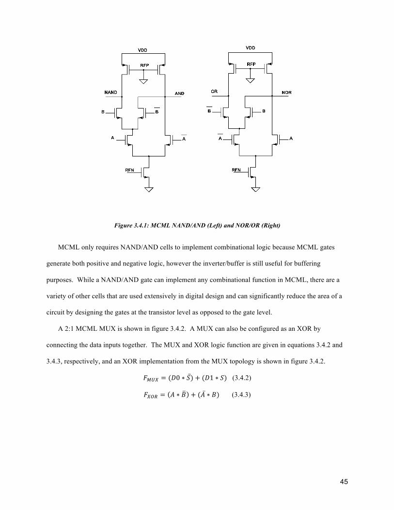
45
Figure 3.4.1: MCML NAND/AND (Left) and NOR/OR (Right)
MCML only requires NAND/AND cells to implement combinational logic because MCML gates
generate both positive and negative logic, however the inverter/buffer is still useful for buffering
purposes. While a NAND/AND gate can implement any combinational function in MCML, there are a
variety of other cells that are used extensively in digital design and can significantly reduce the area of a
circuit by designing the gates at the transistor level as opposed to the gate level.
A 2:1 MCML MUX is shown in figure 3.4.2. A MUX can also be configured as an XOR by
connecting the data inputs together. The MUX and XOR logic function are given in equations 3.4.2 and
3.4.3, respectively, and an XOR implementation from the MUX topology is shown in figure 3.4.2.
𝐹!"# = (𝐷0 ∗ 𝑆) + (𝐷1 ∗ 𝑆) (3.4.2)
𝐹!"# = 𝐴 ∗ 𝐵 + (𝐴 ∗ 𝐵) (3.4.3)
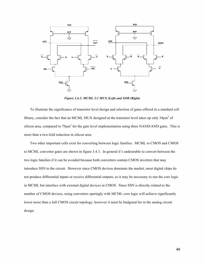
46
Figure 3.4.2: MCML 2:1 MUX (Left) and XOR (Right)
To illustrate the significance of transistor level design and selection of gates offered in a standard cell
library, consider the fact that an MCML MUX designed at the transistor level takes up only 34µm2 of
silicon area, compared to 79µm2 for the gate level implementation using three NAND/AND gates. This is
more than a two-fold reduction in silicon area.
Two other important cells exist for converting between logic families. MCML to CMOS and CMOS
to MCML converter gates are shown in figure 3.4.3. In general it’s undesirable to convert between the
two logic families if it can be avoided because both converters contain CMOS inverters that may
introduce SSN to the circuit. However since CMOS devices dominate the market, most digital chips do
not produce differential inputs or receive differential outputs, so it may be necessary to run the core logic
in MCML but interface with external digital devices in CMOS. Since SSN is directly related to the
number of CMOS devices, using converters sparingly with MCML core logic will achieve significantly
lower noise than a full CMOS circuit topology, however it must be budgeted for in the analog circuit
design.

47
Figure 3.4.3: MCML to CMOS (Left) CMOS to MCML (Right)
Another factor that may influence the use of converters is pin count. Pure MCML circuits require
double the number of inputs and outputs for the differential pairs compared to the equivalent CMOS
circuit. Determining whether or not to interface externally with CMOS versus MCML is a design trade-
off between the interfacing circuitry, pin count, and analog device sensitivity.
Most modern digital circuits are synchronous, which requires a memory storage element. The
simplest storage element is a D-latch. Since latches are difficult to operate due to timing issues, flip-flops
(FF) are the preferred storage element for many digital designers. The most common flip-flop topology is
the DFF, however the MCML implementation of a DFF suffers from transparency issues that cause it to
act like a latch. Thus, an MCML double-edge triggered flip-flop (DETFF) was implemented as proposed
in [18]. The DETFF uses a set of parallel D-latches with opposite polarity clock enables and a MUX with
a clock driven select line. On the rising edge D1 captures the input signal and the MUX chooses the
stored D2 element, then on the following falling edge the MUX selects the stored D1 element while D2
captures the input. The DETFF gate level block diagram description and transistor level circuit is shown
in figure 3.4.4.

48
Figure 3.4.4: DETFF Block Diagram (Left) and Transistor Level Diagram (Right) [18]
The cells discussed in this section illustrate a few key digital gates that are commonly used, and were
chosen to be the starting point for this MCML standard cell library. Binary decision diagrams (BDD) can
be developed for any arbitrary logic function, and they fold directly into an MCML cell. Figure 3.4.5
shows an example by giving the reduced BDD for an and-or-invert (AOI) gate and the resulting pull-
down network implemented in MCML [2]. Equation 3.4.4 shows the Boolean equation for an AOI gate.
𝐹 = 𝐴𝐵 + 𝐶 (3.4.4)

49
Figure 3.4.5: AOI BBD (Left) and MCML Pull-Down Logic (Right)
3.4.2 Methodology for Developing a Family of MCML Cells
Developing MCML cells is a challenging process in which many design iterations may be needed to
converge on the best/optimal design, it takes a large amount of work up front to understand and quantify
the relationship between the design parameters and performance metrics. The results of the simulations
for design tradeoffs as it pertains to voltage swing and current consumption are summarized in table 3.4.1.
Table 3.4.1: Design Tradeoff Summary
Design Modification Effect on Circuit Performance
NMOS pull-down W/L ratios Negligible effect on voltage swing and current
PMOS pull-up W/L ratios Large control over voltage swing, negligible effect on current
Tail current W/L ratio Large control over voltage swing and current
RFN voltage Large control over voltage swing and current
Once the relationships between the components of an MCML gate are understood, it’s relatively easy
to envision the tradeoffs to produce a set of cells aimed at a target application, referred to as a family from
here on. A “family” of MCML cells refers to a set of cells that attempt to address a specific high-level

50
design goal. The success of an MCML standard cell library should be judged on how well it addresses
the breadth of applications that utilize digital circuits. Indirectly, voltage swing and current determine
most other performance metrics for MCML circuits. Common digital circuit performance metrics
include: noise produced, noise margin, speed, power consumption, and area. As an example to
demonstrate the process to develop a family of MCML cells, lets consider the high-level constraints of
low power and high speed for this example, as these are typically high priorities in modern electronics.
The first step in developing a family of MCML cells is to evaluate the repercussions of producing a
circuit that is strictly low power, high speed. If the current is decreased to reduce the power consumption
for a given voltage swing, then the speed decreases. If the voltage swing is decreased for a given current
consumption, then the speed increases but power consumption remains the same. The latter looks like a
good path to pursue since it fixes one design goal while improving the other. For a fixed current
consumption, the pull-up W/L ratio must increase to reduce the voltage swing and therefore the speed. If
the current is too high, the RFN voltage or the tail current W/L ratio can be decreased, both of which
roughly offset each other in terms of speed. Iterating between setting a current and adjusting the voltage
swing should eventually converge on the desired goal, though it neglects the discussion of area, noise
generation, and robustness. These are not the highest priorities, but they still must be considered. Area
will almost always increase, while noise will decrease with lower power and reduced voltage swing,
which is an added benefit of pursuing this design. Power consumption and voltage swing (directly related
to speed) in MCML gates exhibit a logarithmic relationship to transistor area. This logarithmic
relationship says that at some point it becomes infeasible to reduce the power beyond a certain threshold
because the area trade-off will become too large. Reducing the channel length of large devices can save
area but will degrade matching.
This example addresses a single potential design goal, and attempts to optimize two common metrics
in digital design. Many other standard metrics exist, in addition to the metrics discussed previously, and
are summarized with respect to how voltage swing and current consumption can be adjusted to improve
each metric in table 3.4.2.

51
Table 3.4.2: Performance Metrics Tradeoffs Summary
Metric (Optimization Goal) Bias Current Voltage Swing
SSN (Minimize) Decrease Decrease
Power (Minimize) Decrease Negligible
Speed (Maximize) Increase Decrease
Area (Minimize) Depends Depends
Robustness (Maximize) Negligible Increase
CMR (Unity) Negligible Negligible
VSR (Unity) Increase Increase
RFR (Unity) Negligible Decrease
Voltage gain (Maximize) Negligible Increase
LVD (Zero) Negligible Increase

52
CHAPTER 4
Standard Cell Libraries
A standard cell library refers to a collection of digital gates/circuits that have well-defined
performance that allows digital designers to design circuits at a high level of abstraction, namely using a
hardware description language (HDL). Standard cells provide integrated circuit design tools the
information necessary to create and simulate large digital circuits with high degree of confidence that the
circuit generated in HDL will work functionally when laid out in silicon. Cell libraries greatly reduce the
development time and expertise needed for digital circuit design. The digital flow that starts with HDL
code and produces a chip ready for tape-out is shown in figure 4.1.
Figure 4.1: Digital Circuit Design Flow
4.1 Cell Area and Chip Cost
The cost to produce a chip increases significantly with area. Smaller chips increase the number of
chips that can be fabricated per wafer (wafer yield) while also increasing the percentage of functional
chips (die yield), resulting in an exponential decrease in chip cost as a function of area [30]. Cell area has
largely been neglected to this point, yet it is an important metric when designing standard cells. There are
two important points regarding cell area: reducing the area of a single cell can result in significant
reduction in chip area(s), and transistor dimensions do not correlate directly to cell area.

53
Typical VLSI circuits incorporate thousands to hundreds of thousands of standard cells. Even in
extensive standard cell libraries, it’s not uncommon for a single gate to be used hundreds of times in a
circuit. Any reduction in the area of a cell has the potential to return huge savings in chip area,
corresponding directly to cost savings.
It’s possible to create highly optimized gates that have transistors, power rails, and I/O signals
configured to maximize the cell area efficiency, but this would make routing cells together a challenging
process because there would be no consistency. Typically, standard cell constraints lead to a certain
amount of unused space at the cost of simplifying PAR. Unused space generally exists such that it can be
filled with larger transistors without changing the total cell area. For example, it was determined that
increasing the size of the pull-down devices had a negligible affect on cell area, but improved the LVD of
the cell.
Cells should always utilize larger cell widths as opposed to increasing the cell height – it’s desirable
to keep the cell height to the minimum 6.72um. There are two reasons for this; first, if a cell height is
doubled from 6.72um to 13.44um, the area immediately doubles and it’s unlikely the entire area will be
utilized. Increasing the width only increases the area by a fraction of the total because no cell exists that
can fit within 6.72um by 0.56um. Similarly, if a cell can be modified to fit a smaller area, it’s more likely
that the width can be reduced by an integer number of 0.56um than the height can be by 6.72um. This
property is useful if the cell needs to be re-designed in later design iterations or to produce a new family
of cells.
4.2 The Basics of Standard Cells
A standard cell is a digital gate or circuit designed at the silicon level that has been abstracted to allow
for fast, automated design of very-large-scale integrated (VLSI) circuits. Testing and optimization is
crucial in standard cell design because unlike most IC’s that are targeted at a specific application or field

54
of applications, standard cells are designed such that any digital circuit can be implemented for any
application.
4.2.1 Standard Cell Sizing Constraints
A key component to standard cells is their ability to be laid-out in silicon and routed quickly and
efficiently. This is made possible by stringent sizing constraints on the dimensions and geometries of a
standard cell. The sizing constraints for the MCML standard cells are the same as for the IBM 7RF cells,
which allows the 7RF compiler to be used to place-and-route (PAR) MCML cells with minimal
modifications. There exist four hard sizing constraints: cell width, cell height, VDD and GND rail
locations. Hard constraints are constraints the software requires and must be made aware of. Cell width
and height are defined so that cells will not overlap each other and can be easily placed on a grid,
simplifying routing. VDD and GND rail locations are defined such that they will easily overlap with
neighboring cells. There are also soft constraints that define constraints implemented in this standard cell
library that the software does not require, but were chosen to prevent issues when routing large numbers
of cells together. For example, the RFN contact is shared by a large number of MCML gates – having it
at a common point in all MCML cells makes it easy to route these contacts together. Table 4.2.1
summarizes the cell constraints, and figure 4.2.1 shows an arbitrary standard cell layout.

55
Table 4.2.1: Standard Cell Sizing Constraints
Hard Constraint Value
Cell height 6.72um * N
Cell width 0.56um * N
GND rail height (bottom edge, top edge) 0.36um (0.66, 1.02 um)
VDD rail height (bottom edge, top edge) 0.36um (4.58, 4.94 um)
Soft Constraint Value
Power rail overlap on left and right of cell boundary
0.46um
NMOS devices Below VDD
PMOS devices Above VDD
RFN rail height (bottom edge, top edge) 0.3um (0.15, 0.45um)
NWell overlap 0.2um around all sides of VDD and above cell height
BP overlap 0.1um inside NWell and 0.1um above VDD

56
Figure 4.2.1: Arbitrary MCML Standard Cell Layout
4.2.2 Standard Cell Development Methodology
The first step in creating a standard cell is transistor level design followed by functional simulations,
and then a number of design iterations as needed to achieve the desired power consumption, noise
generation, propagation delay, etc. – typically more iterations for more complicated cells. Each cell must
be highly optimized because design flaws existing in a single standard cell can be amplified when cells
are cascaded in long logic chains. These design flaws may cause glitches or logic errors that are not seen
when testing the individual cells or smaller sub-circuits. Once a cell has met functional requirements, it
must be laid out in silicon. The focus in layout is cell density for the reasons discussed previously. To
mitigate process variation in MCML cells, differential pair transistors should sit as close as possible to
each other and in the same orientation.
Layout has two major hurdles: design rule check (DRC) and layout versus schematic (LVS). DRC
checks the layout implementation against rules set by the foundry that ensure the circuit laid out will be
fabricated correctly. DRC errors indicate that the layout implementation would possibly have defects,
and the foundry will not accept designs with DRC errors. LVS checks that the circuit described in the
schematic is connected correctly in the layout. Typically, LVS catches shorts or opens created by missing

57
or inadvertent connections that shouldn’t be present. Passing LVS is not a requirement to have a circuit
fabricated, but it is a good indication that the circuit layout will function as expected from the schematic
level simulations. For the standard cells in this thesis, passing LVS was considered a requirement
because higher-level designs making use of the standard cells will not pass LVS if the lowest level cells
didn’t pass.
Extraction follows successful layout passing DRC and LVS. Extraction models physical properties of
metal interconnects and other material interactions at the silicon level as parasitic resistors, inductors, and
capacitors added to the netlist of the cell schematic, which comprises a more accurate description of the
cells behavior. Post-extraction simulations will provide a more realistic representation of the circuit
performance compared to pre-layout, schematic level simulations.
Extraction coupled with post-extraction testing completes the design-and-test portion of standard cell
development. The next stage involves generating various files know as “cell views” that the software
tools utilize to speed-up the automated digital design flow.
4.2.3 Standard Cell Integration with Virtuoso Digital Design Flow
Adding the standard cells to the software requires generation of cell views that abstract features of the
cell layout for different portions of the tool chain. Cell views stem from layout and extraction views, and
are essentially stripped down versions of these views that tailor their data to specific tools. Abstracting
the cell description allows the tools to perform tasks quicker. For example, the PAR tool doesn’t need all
the technology information present in the layout view, it simply needs to know where blocks are located
to know where it can and cannot route layers. Similarly, Verilog simulation only cares about the timing
performance of the circuit, not the low-level layout information. The cell views required are summarized
in table 4.2.2 and the flow to generate these views is shown in figure 4.2.2.

58
Table 4.2.2: Cell View Summaries
View Description
Extraction Modified schematic netlist to include parasitic RLC's based on layout
Abstract Describes layout as blocks so the place-and-route tool knows where it can
and can't route over the cell
Behavioral Provides timing information to allow for Verilog level simulation of the cell
Liberty (LIB) Summarizes I/O interface, cell logic function, cell parasitics and timing
Library Exchange
Format (LEF)
Provides information about the technology and abstract view to the place-
and-route tool
Figure 4.2.2: Standard Cell Design Flow and File Formats [15]
After all the required cell views are generated, the cells can be added to the IBM library and the
compiler can be modified accordingly. Appendix C discusses how to develop the cell views required for
standard cells to be integrated into the software for automated digital design flow.

59
4.3 Depth of Standard Cell Libraries and Performance Optimization
The depth of a standard cell library is typically measured in gate variety and sizes – cell libraries with
a greater selection of gates can create more efficient circuits because there are more options for
optimization. Variety measures the different flavors of gates available for selection. It is sufficient to
develop a cell library with an inverter, NAND, and DFF cell, because these three cells create the
fundamental building blocks able to produce almost any digital circuit. However, it is always more
efficient to develop gates at the transistor level as opposed to the gate level. Consider an MCML
implementation of an XOR gate: at the transistor level it is implemented with 9 transistors and has 1x
power consumption. At the gate level it takes three gates consisting of 21 transistors, 3x power
consumption, and inevitably operates slower. This is why more developed cell libraries contain a greater
selection of cells that may include: AND, OR, NOR, XOR, AOI, MUX, adders, three-plus input gates,
and other flip-flops (FF). Two advantages of MCML gates are: positive and negative logic outputs for
each gate, and multiple logic functions implementable from a single circuit topology. Put together, this
significantly reduces the number of gates that need to be developed compared to an equivalent CMOS
standard cell library. For example, three MCML gates are capable of implementing the logic of nine
separate CMOS gates.
Complementary to variety is cell size (i.e. drive strength) options. Buses and I/O pins typically
present large capacitive loads and are inefficient to drive from a parallel configuration of multiple low
drive strength gates. Cells offered in different size options allow for high performance circuits that can
implement core logic effectively while also being able to efficiently drive large loads.
MCML standard cells offer a third depth consideration that offers the potential for highly optimized
circuits. Unlike CMOS standard cell libraries in which the only modifiable cell parameter is drive
strength, an MCML standard cell library can offer highly optimized series of cells aimed at specific
applications such as: low noise, low power, high speed, and can trade-off between these three

60
performance metrics, among others. The standard cells developed in this thesis are targeted at two
applications: general-purpose small area, and low noise, low power.
4.4 Comparison of Cells Developed in MCML Standard Cell Library
The two generations of cells developed in this thesis aim to address distinct issues in digital circuit
design. The first generation (“Gen 1”) is a low noise, robust cell with a small area and moderate power
consumption and drive strength. The second generation (“Gen 2”) is aimed at very low noise and low
power applications, and attempts to compensate for the loss in drive strength with a lower voltage swing,
at the cost of robustness and area.
Table 4.4.1 summarizes the cells designed, and compares the performance specs of each. Note that
all cells have minimum cell height of 6.72um. In addition, the MCML to CMOS converter uses the same
layout for both generations, the only change is the input voltage swing applied. The worst-case rise/fall
time was typically the limiting factor in terms of speed, with the exception of the MCML to CMOS
converters, which have much larger propagation delays.

61
Table 4.4.1: Performance Comparison of Gen 1 and Gen 2 MCML Standard Cells
Inverter/Buffer NAND/AND MUX (XOR) Gen 1 Gen 2 Gen 1 Gen 2 Gen 1 Gen 2
Bias Current (µA) 23.95 3.68 23.86 3.63 23.7 3.63 Voltage Swing (mV) 390 180 380 184 378 185 RFN Voltage (mV) 820 680 820 680 820 680 Cell Width (um) 2.8 3.92 3.92 5.04 5.04 6.72 Rise/Fall Time (ps) 52 415 86 588 72 582
DETFF MCML to CMOS CMOS to MCML Gen 1 Gen 2 Gen 1a Gen 1b Gen 1 Gen 2
Bias Current (µA) 55.92 7.01 23 23 23.85 3.7 Voltage Swing (mV) 398 270 1800 1800 389 205 RFN Voltage (mV) 1100 820 820 820 820 680 Cell Width (um) 14 16.24 6.16 6.16 5.04 5.04
Rise/Fall Time (ps) 159 1616 179 (prop)
403 (prop) 40 364
Compared to Gen 1, Gen 2 offers an 85-87% reduction in power and 91% reduction in SSN (section
2.4), at the cost of 680-1010% loss in speed and 14-40% increase in area. Table 4.4.2 gives the transistor
sizes for the two generations of MCML standard cells.
Table 4.4.2: Transistor Dimension Comparison of Gen 1 and Gen 2 MCML Standard Cells
Inverter/Buffer NAND/AND MUX/XOR Gen 1 Gen 2 Gen 1 Gen 2 Gen 1 Gen 2
PMOS Pull-Up W/L (nm) 360/360 360/1440 360/360 360/1440 360/360 360/1440 NMOS Pull-Down W/L (nm) 720/180 720/180 720/180 720/180 720/180 720/180 Tail Current W/L (nm) 720/720 720/2880 720/720 720/2880 720/720 720/2880
DETFF MCML to CMOS CMOS to MCML Gen 1 Gen 2 Gen 1 Gen 2 Gen 1 Gen 2
PMOS Pull-Up W/L (nm) 360/360 360/2880 360/360 360/360 360/360 360/1440 NMOS Pull-Down W/L (nm) 720/180 720/180 720/180 720/180 360/180 720/180 Tail Current W/L (nm) 720/720 720/2880 720/720 720/720 720/720 720/2880 NMOS CLK Pull-Down W/L (nm) 1440/180 1440/180 N/A N/A N/A N/A

62
To reduce the power consumption in the second generation, the tail current device lengths were
increased by a factor of 4 and the RFN voltage was decreased. This alone would reduce the voltage
swing to near zero, thus the pull-up device lengths were increased by a factor of 4 to bring the voltage
swing back up to 200mV. In addition, the total active transistor area increased by 250-300% but the cell
areas only increased by a tenth of those percentages, indicating that using significantly larger transistors
does not always have as severe an impact as it may appear.
Both of these generations exhibit very low SSN compared to CMOS (an order of magnitude reduction
for Gen1 and two orders for Gen2). The first generation is a better choice for high-speed applications, but
is higher power. The second generation is the best choice for very stringent noise requirements, but is
larger area and lower speed.
4.5 MCML Standard Cell Layouts
Designing MCML standard cell layouts to the constraints set on the IBM CMOS library posed a
couple challenges. For CMOS gates, it’s common practice in layout to split the cell between the power
rails and place the PMOS devices in the upper section below VDD rail (in an N-well) and the NMOS
devices in the lower section above GND rail. Splitting the cell in this manor works well due to CMOS
gate symmetry, which requires the same number of PMOS and NMOS devices in the pull-up and pull-
down network, respectively. MCML gates do not exhibit this vertical symmetry, and have only two
PMOS devices (six for the DETFF) for the active load, and variable NMOS devices that depend on the
logic implemented and number of inputs. In addition, most MCML gates have multiple levels of
vertically stacked NMOS levels in addition to a large tail current device. To maximize the area efficiency
of each cell, the PMOS devices were moved to sit above VDD, which reserves the entire space below
VDD for NMOS devices.
The following figures (4.5.1 – 4.5.6) show the layouts for the MCML standard cells discussed in
section 3.4.1. All layouts pass DRC and LVS, with the exception of an acceptable LVS error in the

63
second generation CMOS to MCML converter. For reference, table 4.5.1 defines the color scheme used
for the 7RF process that applies to the cells shown below.
Table 4.5.1: 7RF Color Scheme Summary
7RF has unique rules for body contacts of MOSFET devices. In other processes it is sufficient to
place an active region beneath GND and VDD with a via to create the substrate body connection to the
NMOS and PMOS devices, respectively. In 7RF, the NMOS devices require an explicit component,
SUBCX, in schematic to connect to NMOS body pins. The PMOS body pins are connected to VDD in
schematic, but the body contact must be made to VDD through the PMOS Pcells in layout. Failure to
follow these steps leads to DRC and LVS errors in the design. All standard cell layouts were routed
manually to maximize the area efficiency and minimize routing interconnect lengths when possible.
Layer Description
RX Red
PC Green
M1 Blue
M2 Pink
M3 Teal
BP Brown
NW Yellow

64
4.5.1 MCML Inverter/Buffer Layouts
To understand the physical layouts, compare the annotated first generation MCML inverter/buffer,
figure 4.5.1, to figure 4.2.1 (arbitrary cell layout). All others layouts are structurally similar, but may
differ slightly to optimize area efficiency when possible.
Figure 4.5.1: Annotated MCML Inverter/Buffer Layout

65
Figure 4.5.2: MCML Inverter/Buffer Layouts (Gen1 Left, Gen2 Right)

66
4.5.2 MCML NAND/AND Layouts
Figure 4.5.3: MCML NAND/AND Layouts (Gen1 Left, Gen2 Right)

67
4.5.3 MCML MUX (XOR) Layouts
Figure 4.5.4: MCML MUX Layouts (Gen1 Left, Gen2 Right)

68
4.5.4 MCML DETFF Layouts
Figure 4.5.5: MCML DETFF Layouts (Gen1 Top, Gen2 Bottom)

69
4.5.5 CMOS to MCML Layouts
Figure 4.5.6: CMOS to MCML Layouts (Gen1 Left, Gen2 Right)
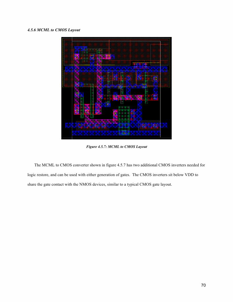
70
4.5.6 MCML to CMOS Layout
Figure 4.5.7: MCML to CMOS Layout
The MCML to CMOS converter shown in figure 4.5.7 has two additional CMOS inverters needed for
logic restore, and can be used with either generation of gates. The CMOS inverters sit below VDD to
share the gate contact with the NMOS devices, similar to a typical CMOS gate layout.
71
CHAPTER 5
Digital Circuits Designed with MCML Standard Cells
Functional testing of standard cells at the individual gate level does not guarantee that the gates will
function properly in a larger digital circuit. To test gates in a more realistic environment, a number of
digital circuits were designed, implemented, and tested for functionality. More complicated circuits were
analyzed using process corners to ensure reliable operation. A few circuits were laid out as well to
illustrate potential implementations of an actual MCML circuit using MCML standard cells.
5.1 MCML 4x4 Multiplier (Gen 1)
A 4-bit multiplier was developed that utilized a broad range of cells from the first generation MCML
gates, including: NAND/AND, XOR, DETFF, CMOS to MCML, and MCML to CMOS. The multiplier
is setup to take CMOS inputs and convert them to MCML, hold them in two 4b MCML registers, perform
all computations in MCML, hold the result in an 8b register, then convert back to CMOS at the output.
The circuit contains a total of 98 MCML gates, broken down as shown in table 5.1.1. The multiplier
utilizes all MCML gates designed with the exception of the inverter/buffer.
Table 5.1.1: Total Gates Implemented in 4b Multiplier
XOR (MUX) NAND/AND DETFF CMOS to MCML
MCML to CMOS
20 45 16 9 8
The topology of the multiplier uses a Dadda tree reduction scheme, followed by a 6b RCA for the two
final operands. The block diagram is shown in figure 5.1.1, and the layout in figure 5.1.2.

72
Figure 5.1.1: MCML 4b Multiplier Block Diagram
Figure 5.1.2: MCML 4b Multiplier Layout View

73
The multiplier cells were laid out by hand and routed automatically to illustrate what a complete
MCML circuit might look like in silicon. The layout is complete with power rings around the design, and
is missing filler cells and biasing circuitry that would be needed if the circuit were being sent to the
foundry for fabrication. Results of testing for the multiplier are summarized in table 5.1.2.
Table 5.1.2: 4b Multiplier Test Results
Input X, Hex (Decimal) Input Y, Hex (Decimal) Output, Hex (Decimal) 0x9 (9) 0x9 (9) 0x51 (81) 0x6 (6) 0x6 (6) 0x24 (36) 0xF (15) 0x9 (9) 0x87 (135) 0x0 (0) 0x6 (6) 0x00 (0) 0x5 (5) 0x3 (3) 0x0F (15) 0xA (10) 0xC (12) 0x78 (120)
Simulations with worst-case parasitics for the MCML multiplier show a maximum SSN of 24.8mV,
comparable to the SSN generated for a single CMOS gate with average parasitics. The largest delay for
the inputs tested was 1.0ns and system current was 2.9mA (5.22mW). After testing corners, it was found
that worst-case speed dropped to 1.16ns and current rose to 3.74mA (6.73mW), with maximum 24.3mV
SSN.
5.2 MCML 16-Bit Carry-Skip Adder (Gen 2)
A 16-bit carry-skip adder (CSA) was developed to test the second-generation MCML gates. The
block diagram is shown in figure 5.2.1, and the total cell count is summarized in table 5.2.1.

74
Figure 5.2.1: 16b CSA Block Diagram
Table 5.2.1: Standard Cells used in 16b MCML CSA
MUX NAND/AND Total 52 60
Simulation results show the transient response of the circuit for the critical path in figure 5.2.2, as
well as the SSN and current for the worst-case parasitics.

75
Figure 5.2.2: 16b MCML CSA SSN (Top) and Transient Response (Bottom)
The results indicate a critical path propagation delay of 5ns. In addition, the circuit only exhibited a
maximum of 1.6mV SSN and 407µA (733µW) current consumption for typical performance. It turns out
the SSN of 1.6mV for the entire 16b CSA is less than the 2.2mV of SSN generated for a single second
generation MCML gate tested (section 2.4.3). This is likely due to the fact that the larger circuit adds
capacitance to the power network, reducing SSN (eq. 2.4.1). Simulation results for the critical path (test
1) as well as three other sets of inputs are summarized in table 5.2.2.
Table 5.2.2: 16b CSA Simulation Results
A, hex (dec) B, hex (dec) A+B, hex (dec) Prop delay (ps) Test 1 0x7FFF (32,767) 0x0001 (1) 0x08000 (32,768) 4980 Test 2 0x8000 (32,768) 0xFFFE (65,534) 0x17FFE (98,302) 4649 Test 3 0x0BA1 (2,977) 0x94F9 (38,137) 0x0A09A (41,114) 2635 Test 4 0xF45E (62,558) 0x6B06 (27,398) 0x15F64 (89,956) 2346

76
Process corners results show power consumption increased by 36% to 553µA (995µW), speed
decreased by 10% (to 5.5ns), and SSN increased 38% (to 2.2mV).
5.3 MCML 9-Stage Ring Oscillator (Gen 1 and Gen 2)
To test the MCML inverter/buffer functionality, a 9-stage ring oscillator was created and simulated
for both generations of cells. The resulting schematic is shown in figure 5.3.1, with an accompanying
simulation transient response seen in figure 5.3.2.
Figure 5.3.1: 9-Stage MCML Ring Oscillator Schematic
Figure 5.3.2: 9-Stage MCML Ring Oscillator Simulation Results (Gen1 Top, Gen2 Bot)
Simulation results show that the first generation oscillator has a frequency of 1.74GHz, compared to
307.5MHz for the second generation. The first generation MCML inverter/buffer has a 6.5 times larger

77
bias current than the second generation. For the same voltage swing, the first generation oscillator should
oscillate about 6.5 times faster, assuming negligible parasitic differences between the two generations.
Since the second generation has a lower voltage swing and larger node capacitance (attributed to larger
pull-up devices), the first generation oscillator oscillates 5.66 times faster.
5.4 MCML 4-Bit Synchronous Counter (Gen 2)
The second generation DETFF’s were tested in a 4-bit synchronous counter. The block diagram is
shown in figure 5.4.1, and the transient response in figure 5.4.2. Figure 5.4.2 shows a functional 4b
counter using second-generation MCML standard cells. The circuit was laid out in silicon as shown in
figure 5.4.3.
Figure 5.4.1: 4b Synchronous Counter Block Diagram

78
Figure 5.4.2: 4b Synchronous Counter Transient Response (Top Down: CLK, B0, B1, B2, B3)

79
Figure 5.4.3: 4b MCML Synchronous Counter Layout using Standard Cells
Figure 5.4.3 shows the counter in silicon using standard cells. The circuit was left unrouted to make
it easier to see the standard cells. In addition to the outer power rails, two smaller rails were placed
around the design to route the RFN voltages needed to drive the DETFF’s and the other gates. This was
determined to be the best way to route the RFN signals since they typically fan-out to a large number of
gates. The RFN rails carry negligible current because they drive the gates of the NMOS tail devices,
allowing them to be smaller width than the power rails.
5.5 Integration of MCML and CMOS Circuits with Analog Devices and Parasitics
An analog voltage-to-current (V-to-I) converter was developed to compare the effects of interfacing
MCML versus CMOS digital circuitry with a sensitive analog device. The simulation environment
consists of the analog circuit sharing the supply and ground of an arbitrary digital circuit modeled as a 10-

80
gate parallel NAND configuration, as shown in figure 5.5.1. There is no communication between the
analog and digital portions since the goal is simply to quantify the effects of SSN applied to the power
network on the sensitive analog circuitry. The SSN is generated by applying an arbitrary set of inputs to
the digital circuit for the best and worst parasitics at different frequencies.
Figure 5.5.1: V-to-I Converter Interfaced with Arbitrary Digital Circuit
The ideal performance of the V-to-I converter in the presence of power network parasitics and
absence of digital circuitry is shown in figure 5.5.2. The simulation run inputs a continuous ramp
function to the V-to-I converter and applies a clock signal to the digital circuitry. The transient response
shows a current ramp output tracking the input voltage, and the power rails at the top and bottom.

81
Figure 5.5.2: Ideal V-to-I Converter Results
Figures 5.5.3 and 5.5.4 below show integration of 10 NAND gates sharing the same supply and
ground as the V-to-I converter for CMOS and MCML for the best and worst parasitics.
Figure 5.5.3: V-to-I Interface with Digital; CMOS Left, MCML Right (5Ω, 1nH, 200fF)

82
Figure 5.5.4: V-to-I Interface with Digital; CMOS Left, MCML Right (2Ω, 4nH, 50fF)
For these simulations, the SSN settled before the next input cycle. The same circuits were tested for
signals switching ten times as fast, and the results are shown in figures 5.5.5 and 5.5.6.
Figure 5.5.5: V-to-I Interface with Digital; CMOS Left, MCML Right (5Ω, 1nH, 200fF, 10x Speed)

83
Figure 5.5.6: V-to-I Interface with Digital; CMOS Left, MCML Right (2Ω, 4nH, 50fF, 10x Speed)
The output range of the V-to-I converter is 0-35µA. CMOS produced up to 3.3µA (best) and
10.63µA (worst) deviation from the expected value for the parasitics tested, while MCML produced max
0.18µA and 0.5µA deviation. The error in the analog circuit is directly correlated to the magnitude of
SSN contributed to the system by the digital circuitry. As expected, CMOS error is an order of
magnitude larger than MCML error, and can make it extremely difficult to interface digital circuits
alongside sensitive analog devices.
5.6 Fabricated Chips Containing MCML Circuits Designed with Standard Cells
Two chips were laid out and accepted by MOSIS for fabrication, a third was developed that passes
DRC and is ready for the next tapeout cycle. The goal of developing chip(s) was two-fold: prove that the
standard cells and circuits designed pass all necessary requirements to be fabricated, and to test the
functionality of real MCML circuits in silicon. Note that for all these chips analog IO pads were chosen
for their simplicity.
5.6.1 Chip 1: MCML and CMOS Inverters, 8b MCML Shift Register
The first chip contains three circuits: 20 parallel CMOS inverters, 20 parallel MCML inverter/buffers,
and an 8-bit MCML shift register, shown between the red blocks in the center of the die in figure 5.6.1.

84
These circuits were chosen for simplicity and minimal pin count – the chip can only contain up to 24
analog IO pads. The inverter configurations are large to drive the high capacitive IO pins.
Figure 5.6.1: Chip 1 Layout
5.6.2 Chip 2: 4b MCML Synchronous Counter
The second chip developed and accepted contains a 4b MCML synchronous counter, and is shown in
figure 5.6.2.

85
Figure 5.6.2: Chip 2 Layout
5.6.3 Chip 3: 99-Stage MCML Ring Oscillators and Individual MCML Gates
The third chip contains optimized circuits to drive the large IO pad capacitances efficiently. A 99-
stage MCML ring oscillator was developed using both the first and second-generation MCML
inverter/buffers. The 99-stages were necessary to lower the oscillation frequency, allowing the buffers to
drive the output pins before switching states. The other circuit contains an MCML NAND/AND, MUX,
and DETFF to test the gates individually. To reduce the number of pins needed the circuit has three input
signals: ‘A’, ‘B’, and ‘SEL’. ‘A’ and ‘B’ are routed into the MUX and NAND/AND. The ‘SEL’ line of
the MUX is also the CLK for the DETFF. The D input to the DETFF is signal ‘A’. The chip layout is
shown in figure 5.6.3. The chip layout passes the same DRC rules run for chip 2, but is pending the next
tapeout date.

86
Figure 5.6.3: Chip 3 Layout

87
CHAPTER 6
Conclusions and Future Work
6.1 Conclusion
MCML gates were analyzed and developed with the primary purpose of providing an alternative to
CMOS logic for noise sensitive, mixed-signal applications. Simulations show that these MCML gates
produce SSN an order of magnitude lower than equivalent CMOS gates, making them a better choice for
mixed signal chips. Testing shows that the MCML gates developed produce real-world, functional digital
circuits in the form of a 4-bit multiplier, 16-bit carry-skip adder, 9-stage ring oscillator, and 8-bit counter.
In addition, these entire MCML circuits produce SSN comparable to only a few CMOS gates. Integration
of an arbitrary digital circuit in both MCML and CMOS with a sensitive analog device showed that
without careful attention paid to isolating the digital and analog components, running digital logic in
CMOS with analog components is not a valid design strategy for high-accuracy systems. On the other
hand, MCML can be laid out alongside analog devices with no isolation whatsoever, and provides a very
low noise digital environment conducive to analog designers.
Analysis of an MCML inverter/buffer looked at the fundamental design parameters for MCML gates:
voltage swing and bias current, and how each component of an MCML gate affects these parameters.
Voltage swing and bias current determine almost all important digital performance metrics for MCML
gates: noise generated (SSN), power consumption, speed, noise margin, etc. Analysis also looked at
potential pitfalls in the form of underestimating system power, gate robustness, propagation of degraded
cells, and more, and how these issues could be mitigated through quality design and layout practices.
A design methodology was developed to speed up the implementation of an MCML standard cell
library. The bulk of the work done for this thesis went towards developing an MCML standard cell
library at the silicon level with a variety of gates in multiple flavors, sufficient to build almost any digital
circuit to suit applications interested in low noise, low power, and minimal area. The MCML cells
88
developed in this standard cell library pass DRC and LVS, and a chip layout containing some of the
MCML gates developed here was accepted and fabricated by MOSIS.
6.2 Future Work
The next step for developing this standard cell library is full integration into the Virtuoso software to
allow for automated design of MCML based digital circuits (fig. 4.2.2). This requires generating all
necessary cell views and adding the cells to the current IBM 7RF standard cell library. The compiler may
need some modifications to make it aware of the difference between the MCML and CMOS standard
cells.
A standard cell library is, almost by definition, never “complete”. It is sufficient to develop a single
set of fundamental digital gates that constitute a functional standard cell library. However, quality
libraries offer gates of different sizes (CMOS) and families targeted at different applications (MCML).
This standard cell library would benefit from a set of high-speed gates to implement gigahertz speed
processing, which is an area in which MCML has an advantage over CMOS in power consumption as
well as noise reduction. The addition of more complex cells would also allow for higher performance
MCML circuits. Strong candidates include: three-plus input gates for NAND/AND, 4:1 MUX, half/full
adders, AOI, etc.
This thesis focused on the application of low noise for the MCML cells designed. However, MCML
has the ability to outperform CMOS in high-speed applications because MCML power consumption is
frequency independent, unlike CMOS. Developing a set of CMOS circuits as a baseline for power
consumption and maximum operating frequency would allow for the design of MCML cells aimed
specifically at outperforming CMOS circuits in multiple areas. This would most likely involve additional
families of MCML cells targeted at, specifically, power consumption and speed.
In order to simplify the process of developing more MCML standard cell families, it would be nice to
have a mathematical model or algorithm to quickly generate optimal transistor sizes and bias voltages

89
given a performance specification. This would allow for, at the very least, back-of-the-envelope
calculations that could put the designer in the ballpark of an optimal cell design given certain
requirements. It would be extremely difficult to accurately quantify all the relationships, but a simple
subset would give a good starting point.

90
REFERENCES
[1] D. Marusiak. “MOS Current Mode Logic (MCML) Analysis for Quiet Digital Circuitry And Creation of a Standard Cell Library for Reducing the Development Time of Mixed-Signal Chips”. M.S. thesis. California State University, San Luis Obispo. 2014.
[2] J. Musicer. An Analysis of MOS Current Mode Logic for Low Power and High Performance Digital
Logic. M.S. thesis. University of California, Berkeley. 2004. [3] A. Shapiro and E. G. Friedman. " MOS Current Mode Logic Near Threshold Circuits." Journal on
Low Power Electronics and Applications, Volume 4, pp. 138 - 152, 2014. [4] E. Brunvand. Digital VLSI Chip Design with Cadence and Synopsis CAD Tools. Boston, MA:
Addison-Wesley, 2010. [5] B. Zimmer. “Introduction to the Custom Design Flow: Building a Standard Cell”. Electrical
Engineering and Computer Science, UC Berkeley, 2013. [Online]. Available: http://bwrcs.eecs.berkeley.edu/Classes/icdesign/ee241_s13/Assignments/lab3-stdcell.pdf. [Accessed: Oct. 11, 2014].
[6] B. Liang, K. Ma, Z. Ding, and X. Fu. “The Structure Design of MOS Current Mode Logic Adder”, in
Proceedings of the 2012 International Conference on Microwave and Millimeter Wave Technology (ICMMT), 5-8 May 2012, Shenzhen, China. Available: IEEE Xplore, http://www.ieee.org. [Accessed: 11 Oct. 2014].
[7] M. Alioto and G. Palumbo. Model and Design of Bipolar and MOS Current-Mode Logic: CML, ECL,
and SCL Digital Circuits. Norwell, MA: Springer, 2005. [8] M. Kothandaraman, P. Kumar, et al. “Current-mode logic buffer with enhanced output swing”. U.S.
Patent 8 441 281, May 14, 2013. [9] MOSIS. “Wafer Electrical Test Data and SPICE Model Parameters: IBM 7RF (0.18 micron)”.
7RF_6LM_AM Spice model parameters. Sep 6, 2013. [10] M. Mizuno, M. Yamashina, et al. “A GHz MOS Adaptive Pipeline Technique Using MOS Current-
Mode Logic.” IEEE Journal of Solid-State Electronics, Volume 31, Issue 6, pp. 784-791, Jun 1996. Available: IEEE Xplore, http://www.ieee.org. [Accessed: 19 Oct. 2014].
[11] M. Santarini. “Cadence rolls custom-IC tools into one platform”. EE Times. Sep. 15, 2003.
[Online]. Available: http://www.eetimes.com. [Accessed: Oct. 26, 2014]. [12] MOSIS. “IBM Fabrication Schedule”. [Online]. Available:
https://www.mosis.com/db/pubf/fsched?org=IBM&year=2015. [Accessed: Oct. 26, 2014]
[13] M. Haselman and S. Hauck. “The Future of Integrated Circuits: A Survey of Nano-Electronics”. University of Washington Electrical Engineering. [Online]. Available: http://www.ee.washington.edu. [Accessed: Dec. 6, 2014].
[14] J. Twomey. “Noise Reduction Is Crucial To Mixed-Signal ASIC Design Success”. Electronic
Design. Oct. 3, 2000. [Online]. Available: http://www.electronicdesign.com. [Accessed: Dec. 5, 2014].

91
[15] C. Patel. "Advanced VLSI Design: Standard Cell Design". Computer Science and Electrical
Engineering, University of Maryland. [Online]. Available: http://www.csee.umbc.edu/~cpatel2/links/641/slides/lect02_std_cells.pdf. [Accessed: Apr. 1, 2015].
[16] N. Haiyan and H. Jianping. "The Layout Implementations of High-Speed Low-Power MCML
Cells". IEEE International Conference on Electronics, Communications and Control (ICECC), pp. 2936-2939, Sep 2011. Available: IEEE Xplore, http://www.ieee.org. [Accessed: Apr. 1, 2015].
[17] S. Vijay et al. "Design and analysis of CMOS Inverter and D Latch MCML Inverter". International
Journal of Advanced Trends in Computer Science and Engineering, Volume 1, No. 5, pp. 139-142, Nov-Dec 2012. Available: WARSE, http://warse.org/pdfs/ijatcse03152012.pdf. [Accessed: Apr. 1, 2015].
[18] T. Kwan and M. Shams. "Design of High-Performance Power-Aware Asynchronous Pipelined
Circuits in MOS Current-Mode Logic". IEEE International Symposium on Asynchronous Circuits and Systems, pp. 23-32, Mar 2005. Available: IEEE Xplore, http://www.ieee.org. [Accessed: Apr. 1, 2015].
[19] Microsemi, Appl. Note AC263, pp. 1-4. [20] K. Tang and E. Friedman. “Simultaneous Switching Noise in On-Chip CMOS Power Distribution
Networks”. IEEE Transactions on Very Large Scale Integration (VLSI) Systems, Volume 10, No. 4, pp. 487-493, Aug 2002. Available: IEEE Xplore, http://www.ieee.org. [Accessed: Apr. 11, 2015].
[21] S. Pithadia and S. More. “Grounding in Mixed-Signal Systems Demystified, Part 1”. Texas
Instruments Incorporated. Q1 2013. [Online]. Available: http://www.ti.com/lit/an/slyt499/slyt499.pdf. [Accessed: Apr. 11, 2015].
[22] Fairchild Semiconductor, Appl. Note 77, pp. 1. [23] A. Danowitz et al. “CPU DB: Recording Microprocessor History”. Association for Computing
Machinery, Volume 55, No. 4, pp. 55-63, Apr 2012. [Online]. Available: http://cpudb.stanford.edu/p55-danowitz.pdf. [Accessed: Apr. 27, 2015].
[24] K. Roebuck. SoC System-on-a-chip: High-impact Strategies - What You Need to Know: Definitions,
Adoptions, Impact, Benefits, Maturity, Vendors. Brisbane, Australia: Emereo Publishing, 2012, pp. 65.
[25] “Worldwide ASIC Market”. Integrated Circuit Engineering Corporation. [Online]. Available:
http://smithsonianchips.si.edu/ice/cd/ASIC98/SECTION4.PDF. [Accessed: Apr. 27, 2015]. [26] J. Rabaey et al. “Digital Integrated Circuits: A Design Perspective, 2nd Edition”. Upper Saddle
River, NJ: Prentice Hall, 2003. [27] ST Microelectronics, Appl. Note 1636, pp. 16. [28] G. Engel. “Bias Circuit”. Department of Electrical and Computer Engineering, Southern Illinois
University Edwardsville. [Online]. Available: http://www.siue.edu/~gengel/ece584WebStuff/CurrentMirrors.pdf. [Accessed: Apr. 29, 2015].
92
[29] C. Patel. “Advanced VLSI Design: Quality Metrics of a Digital Design”. Computer Science and Electrical Engineering, University of Maryland. [Online]. Available: http://www.csee.umbc.edu/~cpatel2/links/640/lectures/lect03_qual_metrics.pdf. [Accessed: May 4, 2015].
[30] D. Sorin. “Performance”. Electrical and Computer Engineering and Computer Science, Duke
University. [Online]. Available: http://people.ee.duke.edu/~sorin/prior-courses/ece152-spring2005/lectures/8.2-performance.pdf. [Accessed: May 6, 2015].
[31] R. Harrison. “Differential Pair Layout”. Department of Electrical and Computer Engineering,
University of Utah. [Online]. Available: http://www.ece.utah.edu/~harrison/ece5720/Common_Centroid.pdf. [Accessed: May 7, 2015].
[32] D. Nenni. “Semiconductor Process Variation Wiki”. SemiWiki: The Open Forum for Semiconductor
Professionals. [Online]. Available: https://www.semiwiki.com/forum/showwiki.php?title=Semi%20Wiki:Semiconductor%20Process%20Variation%20Wiki. [Accessed: May 16, 2015].

93
APPENDICES
APPENDIX A
Effects of Parasitic Magnitudes on SSN
Looking at the extreme cases of the parasitics shows the dependence of SSN on the magnitude of
each parasitic element. The results are summarized in table A.1. In general SSN reduces with increased
parasitic capacitance and scales with inductance. Table A.2 shows the numerical results presented in
figure 2.4.10.
Table A.1: Analysis Results of SSN Dependence on Parasitic Elements
Analysis Result Consequence
lim!→!
𝑍!" 𝑅 + 𝑠𝐿 Increases in R and L both cause linear increases in SSN (verified)
lim!→!
𝑍!" 0 SSN = 0 (verified)
lim!→!
𝑍!" 𝑅𝑠𝑅𝐶 + 1
SSN decreases with C, depends on R
lim!→!,!→!
𝑍!" 0 SSN = 0
lim!→!,!→!
𝑍!" 1𝑠𝐶
SSN decreases with C
lim!→!
𝑍!" 1𝑠𝐶
SSN decreases with C
lim!→!
𝑍!" 𝑠𝐿𝑠!𝐿𝐶 + 1
SSN decreases with C, depends on L
lim!→!
𝑍!" 1𝑠𝐶
SSN decreases with C

94
Table A.2: SSN Noise Comparison Summary
Number of Parallel Gates
Parasitic R (Ω)
Parasitic L (nH)
Parasitic C (fF)
MCML Max Noise Induced (mV)
CMOS Max Noise Induced (mV)
1 2 1 50 1.8 23 1 2 4 50 3.6 50 1 2 1 200 0.9 6 1 2 4 200 2.2 15 1 5 1 50 1.6 22 1 5 4 50 3.3 41 1 5 1 200 0.9 6 1 5 4 200 2.2 9 10 2 1 50 12.5 221 10 2 4 50 24.5 251 10 2 1 200 7.2 97 10 2 4 200 17.5 118 10 5 1 50 13.2 206 10 5 4 50 24.3 234 10 5 1 200 8.1 82 10 5 4 200 17.7 125

95
APPENDIX B
Process Variation Analysis using Corners
The NMOS and PMOS FET’s were characterized in terms of their threshold voltages for typical, fast,
and slow performance. For these tests it was decided that 1µA constituted a sufficient amount of current
to consider the device out of cutoff. Once the threshold voltages were measured, they were used to
generate calculated results and compare with the measured results for the corners analysis on the MCML
inverter/buffer. The parameters used for calculations include measured threshold voltages, nominal
transistor dimensions, and k’ parameters as defined in MOSIS test data [9]. Combined with equations
3.1.5 and 3.1.2 this information allows for the calculation of bias current and voltage swing. Tables B.1
and B.2 show the parameters used for calculations, and table B.3 shows the results of these calculations
compared to measured gate performance using process corners.
Table B.1: Tail Current Device Parameters and IDS (ISS) Calculation Results
Corner k’n (µA/V2) W (nm) L (nm) VGS (V) Vtn (V) IDS (µA)
tt 157.8 720 720 0.82 0.391 29.0 sf 157.8 720 720 0.82 0.428 24.2 fs 157.8 720 720 0.82 0.345 35.6 ss 157.8 720 720 0.82 0.428 24.2 ff 157.8 720 720 0.82 0.345 35.6
Table B.2: Pull-Up Device Parameters and VSD (ΔV) Calculation Results
Corner VSG (V) |Vtp| (V)
VOD (V)
W (nm) L (nm)
k’p (µA/V^2)
ISD (µA) VSD (V)
tt 1.8 0.512 1.288 360 360 33.2 29.0 0.402 sf 1.8 0.45 1.35 360 360 33.2 24.2 0.305 fs 1.8 0.576 1.224 360 360 33.2 35.6 0.571 ss 1.8 0.576 1.224 360 360 33.2 24.2 0.348 ff 1.8 0.45 1.35 360 360 33.2 35.6 0.484

96
Table B.3: Results of Simulated vs. Mathematically Calculated Performance of MCML Inverter/Buffer
Corner ISS (µA) ΔV (V)
Calculated Measured % Error Calculated Measured % Error tt 29.0 24.0 17.4 0.402 0.390 3.09 sf 24.2 20.0 17.5 0.305 0.280 8.18 fs 35.6 28.9 18.8 0.571 0.590 3.24 ss 24.2 19.0 21.6 0.348 0.350 0.65 ff 35.6 31.1 12.6 0.484 0.460 4.94
Results indicate that the error was relatively large for the bias current and small for voltage swing.
There are a number of reasons that could contribute to the error in calculations. For example, it was
assumed that the body effect and channel length modulation were both negligible to simplify the
calculations, and the transistor dimensions were assumed nominal when in reality corners changes the
effective dimensions. In addition, the most recent MOSIS test data likely differs from Virtuoso’s
transistor models. It’s possible to perform back-of-the-envelope calculations for an MCML gates
performance, or to design an MCML gate given certain performance specs, but the results will only be an
estimate. Fine-tuning in Virtuoso will be necessary to converge on the optimal design.

97
APPENDIX C
Cell View Generation
The following sections summarize how to develop the cell views needed to develop a complete
standard cell library. It is assumed that the starting point for this is a layout for each standard cell that
passes DRC. The format for these sections is as follows: instruction for how to navigate to the proper
tool, tabulated summary of how to fill in the appropriate fields, screenshot of a filled out tool (as it
pertains to my specific library/file names), and screenshot of an example output of that tool.
C.1 Abstract
𝐼𝑛 𝐶𝐼𝑊 :𝑇𝑜𝑜𝑙𝑠 → 𝐴𝑏𝑠𝑡𝑟𝑎𝑐𝑡 𝐺𝑒𝑛𝑒𝑟𝑎𝑡𝑜𝑟…
Table C.1.1: Abstract Generator Tool Summary
Field Comment
Generate Abstracts for Library Select the library containing the layouts of the
standard cells in the pull-down menu
Figure C.1.1: Abstract Generator Tool View
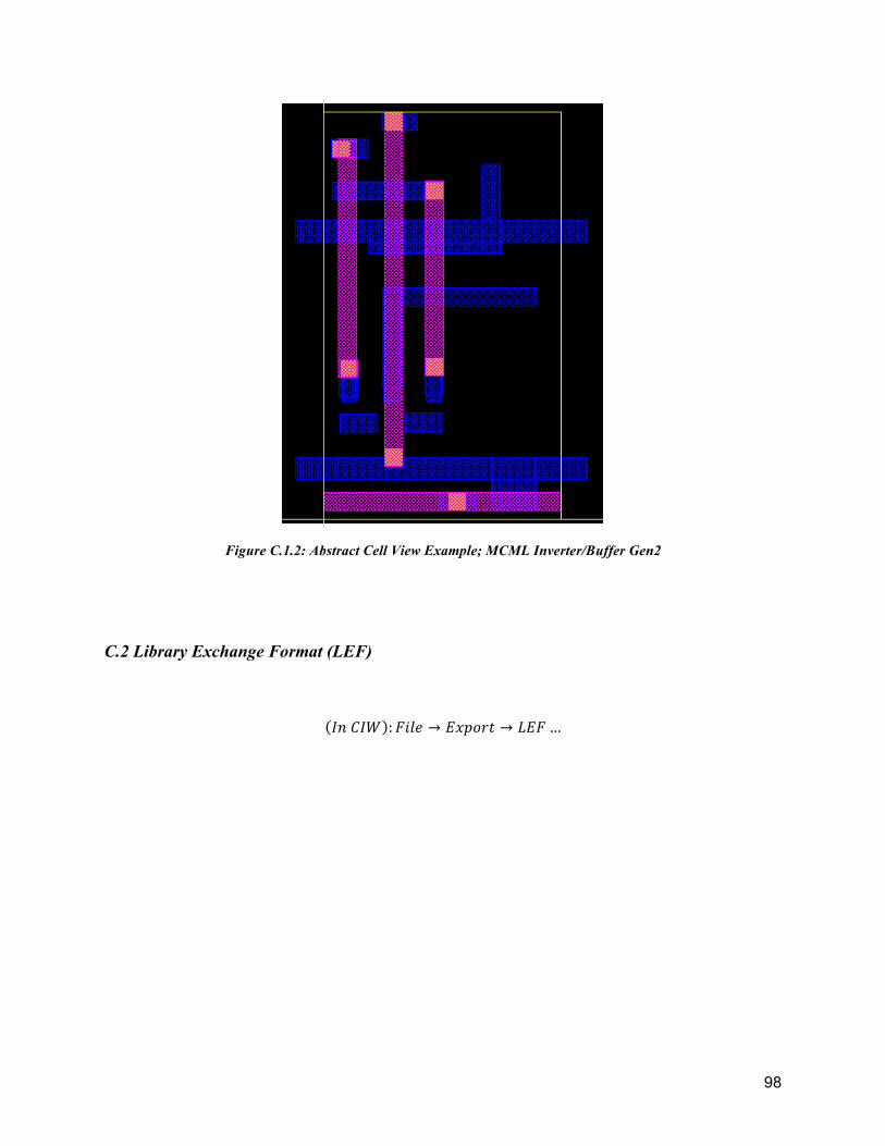
98
Figure C.1.2: Abstract Cell View Example; MCML Inverter/Buffer Gen2
C.2 Library Exchange Format (LEF)
𝐼𝑛 𝐶𝐼𝑊 :𝐹𝑖𝑙𝑒 → 𝐸𝑥𝑝𝑜𝑟𝑡 → 𝐿𝐸𝐹…

99
Table C.2.1: LEF Generator Tool Summary
Field Comment
LEF File Name Enter the name you would like the LEF file to be
called with the extension “.lef”
Library Name Select the same library the abstracts were generated
for in the pull-down menu
Output Cell(s) Click the “…” and choose “Select All”. The list
should contain all the standard cells if the correct
library was chosen
Log File Name Enter a name for the log file to be generated
/Others/ Leave blank/default

100
Figure C.2.1: LEF Generator Tool View

101
Figure C.2.2: LEF Cell View Example; MCML Inverter/Buffer Gen1
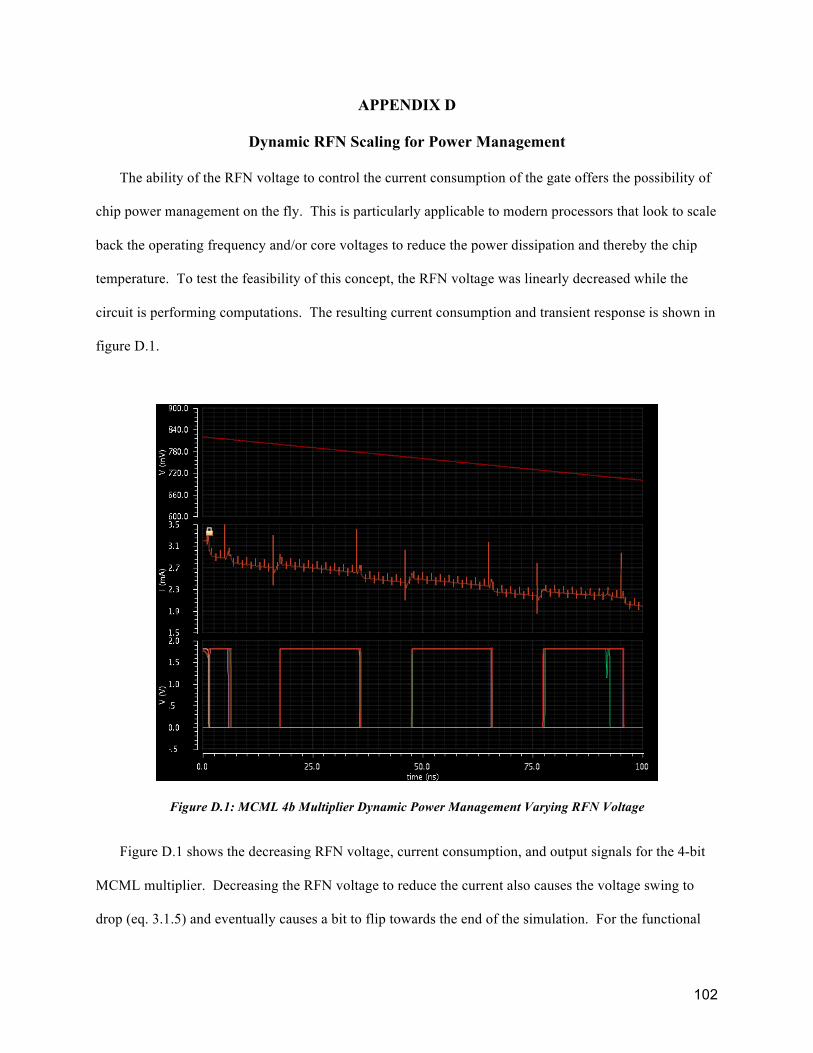
102
APPENDIX D
Dynamic RFN Scaling for Power Management
The ability of the RFN voltage to control the current consumption of the gate offers the possibility of
chip power management on the fly. This is particularly applicable to modern processors that look to scale
back the operating frequency and/or core voltages to reduce the power dissipation and thereby the chip
temperature. To test the feasibility of this concept, the RFN voltage was linearly decreased while the
circuit is performing computations. The resulting current consumption and transient response is shown in
figure D.1.
Figure D.1: MCML 4b Multiplier Dynamic Power Management Varying RFN Voltage
Figure D.1 shows the decreasing RFN voltage, current consumption, and output signals for the 4-bit
MCML multiplier. Decreasing the RFN voltage to reduce the current also causes the voltage swing to
drop (eq. 3.1.5) and eventually causes a bit to flip towards the end of the simulation. For the functional

103
stage of this simulation, the system current was reduced from 3.2mA to 2.2mA – a 31% reduction in
power consumption. The same concept was tested on an MCML inverter/buffer, but the error was
addressed by offsetting the voltage swing reduction seen in the multiplier by increasing the RFP voltage.
The simulation results are shown in figure D.2.
Figure D.2: MCML Inverter Dynamic Power Management, RFP/RFN Offset
Figure D.2 shows the current consumption, RFN and RFP voltages, and input/output signals. For this
simulation, the rate of change of the RFP voltage was set such that it roughly offset the voltage drop as a
result of reducing the bias current. The end result is a 53% reduction in power consumption without the
potential for a logic error. However, the speed decreases by 49% as a result of the voltage swing being
nearly constant while the bias current is reduced. The cells in this thesis do not allow for changes in the
RFP voltage, but this is an implementation that could be made for a separate family of MCML cells.