lecture 9 –mos logic and gate circuitseen.iust.ac.ir/profs/abrishamifar/digital integrated circuit...
TRANSCRIPT

Adib AbrishamifarEE Department
IUST
Lecture 9 – MOS Logic and Gate Circuits
Digital Integrated Circuit Design
A
Y
A
BAB
A
A
Wired OR

IUST: Digital IC Design LECTURE 9 : MOS LogicLECTURE 9 : MOS Logic Adib Abrishamifar 20082/126
} Introduction} NMOS Logic
} Resistive Load } Saturated Enhancement Load} Linear Enhancement Load} Depletion Load} Some Gates} Transient in NMOS Circuit} Pseudo-NMOS
} CMOS Logic} Static CMOS Logic Gates
• NOT• NAND• NOR• Realization of More Complicated Gate Circuits
} Transmission Gates Family• NMOS Only Switch• CMOS
} Differential Cascode Voltage Switch Logic} Rules of Thumb
} Summary
Contents

IUST: Digital IC Design LECTURE 9 : MOS LogicLECTURE 9 : MOS Logic Adib Abrishamifar 20083/126
} The MOS inverter is the basic circuit exhibits all of the essential features of MOS Logic. Extension of MOS inverter concepts to NOR and NAND Gate is very simple. In this lecture we will analysis for VTC, NM, PD,… . Both NMOS and CMOS circuits are considered. Digital MOS circuits can be classified into two categories:} Static Circuits: require no clock or other periodic signal for
operation. Clocks are required for static circuit in sequential logic
} Dynamic Circuits: require periodic clock signals, synchronized with data signals, for proper operation even in combinational logic
Introduction

IUST: Digital IC Design LECTURE 9 : MOS LogicLECTURE 9 : MOS Logic Adib Abrishamifar 20084/126
} Introduction} NMOS Logic
} Resistive Load} Saturated Enhancement Load} Linear Enhancement Load} Depletion Load} Some Gates} Transient in NMOS Circuit} Pseudo-NMOS
} CMOS Logic} Static CMOS Logic Gates
• NOT• NAND• NOR• Realization of More Complicated Gate Circuits
} Transmission Gates Family• NMOS Only Switch• CMOS
} Differential Cascode Voltage Switch Logic} Rules of Thumb
} Summary
Contents

IUST: Digital IC Design LECTURE 9 : MOS LogicLECTURE 9 : MOS Logic Adib Abrishamifar 20085/126
Vdd+
Vo
Vi
RL
Vo
VioOLV
Vdd
NMOS Logic
} Resistive Load
W VoL C SpeedL
P RL Area
↑⇒ ↓⇒ ↑⇒ ↓
↓⇒ ↑⇒ ↑

IUST: Digital IC Design LECTURE 9 : MOS LogicLECTURE 9 : MOS Logic Adib Abrishamifar 20086/126
NMOS Logic
} Resistive Load Properties} N transistors + Load} VOH = Vdd} VOL = Vdd ( rN/(rN + RL))} Assymetrical response} Static power consumption} tPL = 0.69RLCL

IUST: Digital IC Design LECTURE 9 : MOS LogicLECTURE 9 : MOS Logic Adib Abrishamifar 20087/126
} Introduction} NMOS Logic
} Resistive Load } Saturated Enhancement Load} Linear Enhancement Load} Depletion Load} Some Gates} Transient in NMOS Circuit} Pseudo-NMOS
} CMOS Logic} Static CMOS Logic Gates
• NOT• NAND• NOR• Realization of More Complicated Gate Circuits
} Transmission Gates Family• NMOS Only Switch• CMOS
} Differential Cascode Voltage Switch Logic} Rules of Thumb
} Summary
Contents

IUST: Digital IC Design LECTURE 9 : MOS LogicLECTURE 9 : MOS Logic Adib Abrishamifar 20088/126
Vo
Vi
Vdd+ Vdd+
M2
M1Vo
VioOLV
OHV
Vo 1Vi
δ= −
δ
R∝ β
ILVIHV
NMOS Logic
} Saturated Enhancement Load
T2
Vds2 Vgs2Vds2 Vgs2 VM2 is in saturation
= ⇒
> − ⇒

IUST: Digital IC Design LECTURE 9 : MOS LogicLECTURE 9 : MOS Logic Adib Abrishamifar 20089/126
} Saturated Enhancement Load} VIL
IL T12 2
1 T1 2 T2
I 1
T
R
L
2
T
R
V V M1, M2 are in saturation
K (Vgs1 V ) K (Vgs2 V ) , V CteVoVgs1 Vi, Vgs2 Vdd Vo , 1Vi
Vo 1Vi
V V
≥ ⇒
⇒ − = − ≈δ
= = − ⇒ = − β β >δ
δ⇒− ≈⇒ ≠
δ
NMOS Logic
Vo
VioOLV
OHV
Vo 1Vi
δ= −
δ
R∝ β
ILVIHV

IUST: Digital IC Design LECTURE 9 : MOS LogicLECTURE 9 : MOS Logic Adib Abrishamifar 200810/126
} Saturated Enhancement Load} VOL
• VOL is difficult to obtain because it is the output voltage when input equal to VOH, the resulting expression is a fourth order polynomial!
NMOS Logic
Vo
VioOLV
OHV
Vo 1Vi
δ= −
δ
R∝ β
ILVIHV

IUST: Digital IC Design LECTURE 9 : MOS LogicLECTURE 9 : MOS Logic Adib Abrishamifar 200811/126
NMOS Logic
( )
( )
1
1
21 1 T1
22 2 T2
11
iVo rds1 rds2Vi Vi
Vords1 rds2 rds1i
i K Vgs1 V Vo Vo 2
1i K (Vgs2 V )2i
K VoVi
δδ= −
δ δδ
≈ =δ
= − −
= −
δ⇒ =
δ
} Saturated Enhancement Load} VIH
• M1 is in triode and M2 in saturation
( )11 T1
1
1 T1
T1
IH T1IH
iK Vgs1 V Vo
VoK VoVo 1
Vi K (Vgs1 V Vo)Vi V
Vo2V V
Vi V Vo2
δ⇒ = − −
δδ
⇒ = − = −δ − −
−⇒ =
−= ⇒ =

IUST: Digital IC Design LECTURE 9 : MOS LogicLECTURE 9 : MOS Logic Adib Abrishamifar 200812/126
( )1 2
2 21 IH T1 2 T2
T2IH T1
R
i i1K V V Vo Vo 2 K (Vdd Vo V )2
2(Vdd V )V V
3 1
= ⇒
− − = − −
−⇒ = +
β +
NMOS Logic
} Saturated Enhancement Load} VIH
• M1 is in triode and M2 in saturation

IUST: Digital IC Design LECTURE 9 : MOS LogicLECTURE 9 : MOS Logic Adib Abrishamifar 200813/126
IL OL
OH IH T2 IH
NML V V Some tenth of voltNMH V V Vdd V V
= − ≈
= − = − −
NMOS Logic
} Saturated Enhancement Load} NM
} Power
disH disL d
dis d
P 0, P I Vdd
P 1 2I Vdd
≈ =
⇒ =

IUST: Digital IC Design LECTURE 9 : MOS LogicLECTURE 9 : MOS Logic Adib Abrishamifar 200814/126
} Introduction} NMOS Logic
} Resistive Load } Saturated Enhancement Load} Linear Enhancement Load} Depletion Load} Some Gates} Transient in NMOS Circuit} Pseudo-NMOS
} CMOS Logic} Static CMOS Logic Gates
• NOT• NAND• NOR• Realization of More Complicated Gate Circuits
} Transmission Gates Family• NMOS Only Switch• CMOS
} Differential Cascode Voltage Switch Logic} Rules of Thumb
} Summary
Contents

IUST: Digital IC Design LECTURE 9 : MOS LogicLECTURE 9 : MOS Logic Adib Abrishamifar 200815/126
Vo
Vi
VGG
Vdd+
M2
M1
NMOS Logic
} Linear Enhancement Load
Linear Enhancement Load
T2VGG Vdd V
M2 is in triode
≥ +
⇒

IUST: Digital IC Design LECTURE 9 : MOS LogicLECTURE 9 : MOS Logic Adib Abrishamifar 200816/126
NMOS Logic
Vo
VioOLV
Vdd
ILVIHVTVVdd
} Linear Enhancement Load} VTC
• By this circuit the VOHcan be increased (or Vddcan be decreased because Vomax = Vdd )

IUST: Digital IC Design LECTURE 9 : MOS LogicLECTURE 9 : MOS Logic Adib Abrishamifar 200817/126
} Linear Enhancement Load} VIL
• M1 is in saturation and M2 in triode
} VIH • M1 and M2 are in triode
( )
( )
1 1
1
22 2 T2
22 T2
i iVo Vds2rds2Vi Vi Vi i
i K Vgs2 V Vds2 Vds2 2
iK VGG Vo V Vds2
Vds2
δ δδ δ= − = −
δ δ δ δ
= − − δ
= − − −δ
( )
21 1 T1
11 T1
1 T1
2 T2
IL
1i K (Vi V )2
i K Vi VVi
K (Vi V )Vo 1Vi K (VGG Vo V Vds2)
V f (Vo)
= −
δ= −
δ− −δ
= − =δ − − −
⇒ =
NMOS Logic
rds2 rds1 rds2→

IUST: Digital IC Design LECTURE 9 : MOS LogicLECTURE 9 : MOS Logic Adib Abrishamifar 200818/126
Rβ
NMOS Logic
} Linear Enhancement Load} Disadvantages:
• More chip area is required (since an extra voltage source VGG)• Additional interconnection on the chip is needed• The required value of is even larger than a saturated load
Vo
Vi
VGG
Vdd+
M2
M1

IUST: Digital IC Design LECTURE 9 : MOS LogicLECTURE 9 : MOS Logic Adib Abrishamifar 200819/126
} Introduction} NMOS Logic
} Resistive Load } Saturated Enhancement Load} Linear Enhancement Load} Depletion Load} Some Gates} Transient in NMOS Circuit} Pseudo-NMOS
} CMOS Logic} Static CMOS Logic Gates
• NOT• NAND• NOR• Realization of More Complicated Gate Circuits
} Transmission Gates Family• NMOS Only Switch• CMOS
} Differential Cascode Voltage Switch Logic} Rules of Thumb
} Summary
Contents

IUST: Digital IC Design LECTURE 9 : MOS LogicLECTURE 9 : MOS Logic Adib Abrishamifar 200820/126
NMOS Logic
} Depletion Load} Ion implantation processing step is needed to create
depletion device, but overcome the disadvantages of the previous circuit
Vo
Vi M1
Vdd+
M2

IUST: Digital IC Design LECTURE 9 : MOS LogicLECTURE 9 : MOS Logic Adib Abrishamifar 200821/126
NMOS Logic
} Depletion Load} VTC
} Therefore M2 is in triode
1 1 2
222 T2 2
Vi Low i 0, M1 in cutoff i i 0Kif M2 is in saturation then i (Vgs2 V ) ,Vgs2 0 i 02
= ⇒ = ⇒ = =
= − = ⇒ >
Vo
VioOLV
Vdd
ILVIHVTVVdd
IUST: Digital IC Design LECTURE 9 : MOS LogicLECTURE 9 : MOS Logic Adib Abrishamifar 200822/126
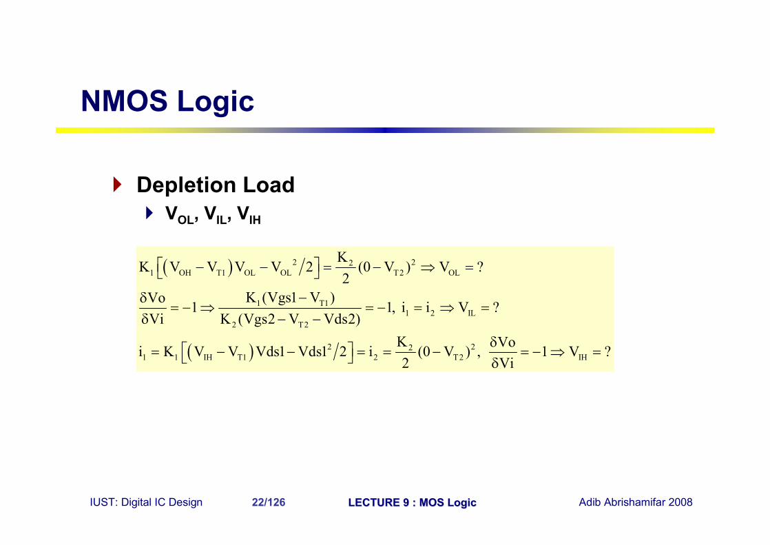
} Depletion Load} VOL, VIL, VIH
NMOS Logic
( )
( )
2 221 OH T1 OL OL T2 OL
1 T11 2 IL
2 T2
2 221 1 IH T1 2 T2 IH
KK V V V V 2 (0 V ) V ?
2K (Vgs1 V )Vo 1 1, i i V ?
Vi K (Vgs2 V Vds2)K Voi K V V Vds1 Vds1 2 i (0 V ) , 1 V ?2 Vi
− − = − ⇒ =
−δ= − ⇒ = − = ⇒ =
δ − −
δ = − − = = − = − ⇒ = δ
IUST: Digital IC Design LECTURE 9 : MOS LogicLECTURE 9 : MOS Logic Adib Abrishamifar 200823/126
} Introduction} NMOS Logic
} Resistive Load } Saturated Enhancement Load} Linear Enhancement Load} Depletion Load} Some Gates} Transient in NMOS Circuit} Pseudo-NMOS
} CMOS Logic} Static CMOS Logic Gates
• NOT• NAND• NOR• Realization of More Complicated Gate Circuits
} Transmission Gates Family• NMOS Only Switch• CMOS
} Differential Cascode Voltage Switch Logic} Rules of Thumb
} Summary
Contents

IUST: Digital IC Design LECTURE 9 : MOS LogicLECTURE 9 : MOS Logic Adib Abrishamifar 200824/126
} Some Gates} In all previous structures which different only in load,
the following Gates can be implemented. Note that the NMOS Gates are not available as separately packaged individual circuits, but they are used extensively in LSI systems
• NOR Gates• NAND Gates
NMOS Logic

IUST: Digital IC Design LECTURE 9 : MOS LogicLECTURE 9 : MOS Logic Adib Abrishamifar 200825/126
} Some Gates} NOR Gate
NMOS Logic
A M1Y
B M2
Vdd+
RL YA
B

IUST: Digital IC Design LECTURE 9 : MOS LogicLECTURE 9 : MOS Logic Adib Abrishamifar 200826/126
} Some Gates} NAND Gate
NMOS Logic
B
A
Vdd+
M2
M1
YRL
A
B
Y
IUST: Digital IC Design LECTURE 9 : MOS LogicLECTURE 9 : MOS Logic Adib Abrishamifar 200827/126
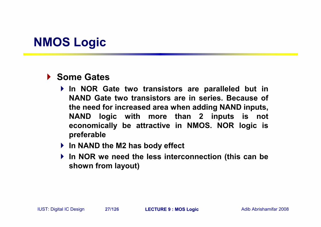
} Some Gates} In NOR Gate two transistors are paralleled but in
NAND Gate two transistors are in series. Because of the need for increased area when adding NAND inputs, NAND logic with more than 2 inputs is not economically be attractive in NMOS. NOR logic is preferable
} In NAND the M2 has body effect} In NOR we need the less interconnection (this can be
shown from layout)
NMOS Logic

IUST: Digital IC Design LECTURE 9 : MOS LogicLECTURE 9 : MOS Logic Adib Abrishamifar 200828/126
} Introduction} NMOS Logic
} Resistive Load } Saturated Enhancement Load} Linear Enhancement Load} Depletion Load} Some Gates} Transient in NMOS Circuit} Pseudo-NMOS
} CMOS Logic} Static CMOS Logic Gates
• NOT• NAND• NOR• Realization of More Complicated Gate Circuits
} Transmission Gates Family• NMOS Only Switch• CMOS
} Differential Cascode Voltage Switch Logic} Rules of Thumb
} Summary
Contents

IUST: Digital IC Design LECTURE 9 : MOS LogicLECTURE 9 : MOS Logic Adib Abrishamifar 200829/126
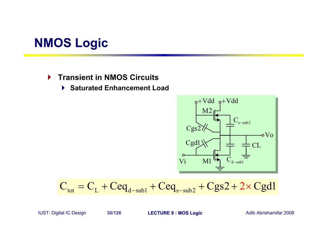
NMOS Logic
} Transient in NMOS Circuits} Saturated Enhancement Load
• For transient calculation we need the total capacitance in output. Some of these are voltage dependent. For all of these:
( ) ( )12 1 1o jo 2 2
eq o o
2 CQ Q(V2) Q(V1)C V2 V1V V2 V1 V2 V1
− Φ∆ − = = = Φ − − Φ − ∆ − −
IUST: Digital IC Design LECTURE 9 : MOS LogicLECTURE 9 : MOS Logic Adib Abrishamifar 200830/126
NMOS Logic
} Transient in NMOS Circuits} Saturated Enhancement Load
tot L d sub1 s sub2C C Ceq Ceq Cgs2 Cgd2 1− −= + + + + ×
Vdd+Vdd+
M1
M2
Vi
Cgs2
Cgd1
s sub2C −
d sub1C −
CLVo
IUST: Digital IC Design LECTURE 9 : MOS LogicLECTURE 9 : MOS Logic Adib Abrishamifar 200831/126
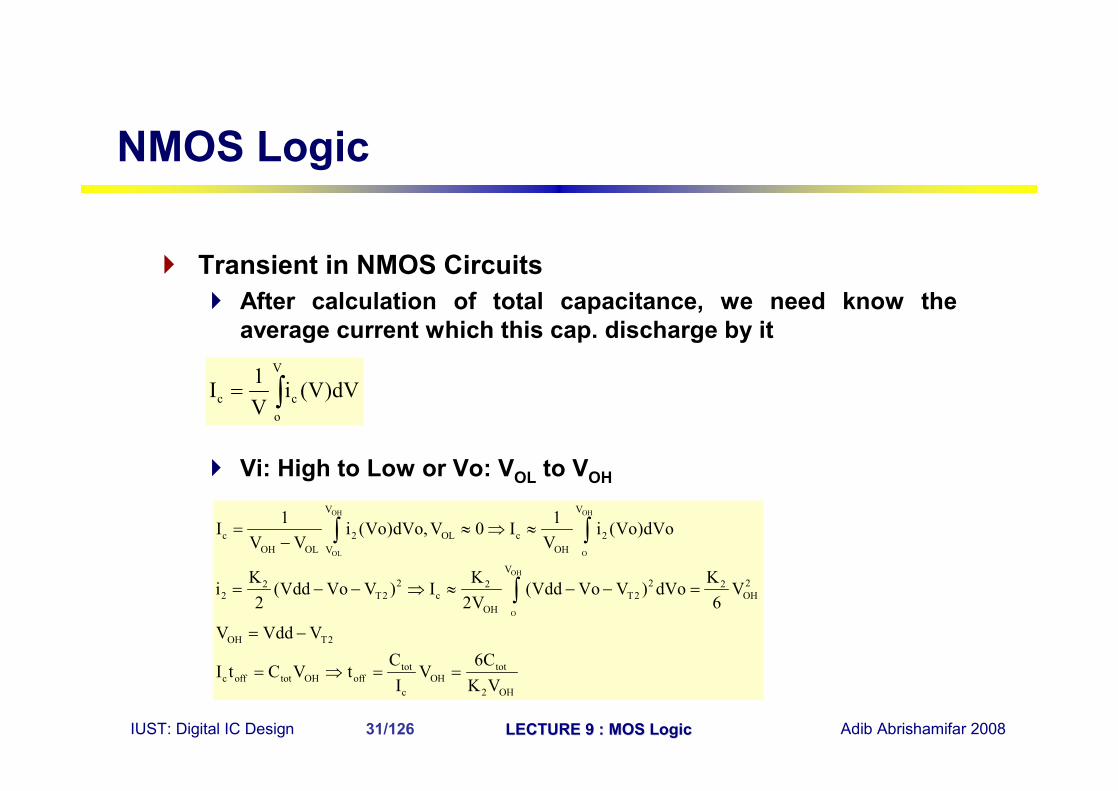
NMOS Logic
} Transient in NMOS Circuits} After calculation of total capacitance, we need know the
average current which this cap. discharge by it
} Vi: High to Low or Vo: VOL to VOH
V
c co
1I i (V)dVV
= ∫
OH OH
OL O
OH
O
V V
c 2 OL c 2OH OL OHV
V2 2 22 2 2
2 T2 c T2 OHOH
OH T2
tot totc off tot OH off OH
c 2 OH
1 1I i (Vo)dVo, V 0 I i (Vo)dVoV V V
K K Ki (Vdd Vo V ) I (Vdd Vo V ) dVo V
2 2V 6
V Vdd VC 6C
I t C V t VI K V
= ≈ ⇒ ≈−
= − − ⇒ ≈ − − =
= −
= ⇒ = =
∫ ∫
∫
IUST: Digital IC Design LECTURE 9 : MOS LogicLECTURE 9 : MOS Logic Adib Abrishamifar 200832/126
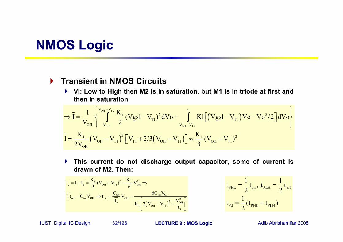
NMOS Logic
} Transient in NMOS Circuits} Vi: Low to High then M2 is in saturation, but M1 is in triode at first and
then in saturation
} This current do not discharge output capacitor, some of current is drawn of M2. Then:
( )
( ) ( )
OH T 2
OH OH T 2
V V o2 21
T1 T1OH V V V
2 21 1OH T1 T1 OH T1 OH T1
OH
K1I (Vgs1 V ) dVo K1 Vgs1 V Vo Vo 2 dVoV 2
K KI V V V 2 3 V V (V V )2V 3
−
−
⇒ = − + − −
= − + − ≈ −
∫ ∫
( )
2 21 2c 2 OH T1 OH
tot tot OHc on tot OH on OH 2
2c OH1 OH T1
R
K KI I I (V V ) V
3 6C 6C V
I t C V t VI VK 2 V V
= − = − − ⇒
= ⇒ = =
− − β
PHL on PLH off
Pd PHL PLH
1 1t t , t t2 2
1t (t t )2
= =
= +

IUST: Digital IC Design LECTURE 9 : MOS LogicLECTURE 9 : MOS Logic Adib Abrishamifar 200833/126
} Super Buffer (1)} If Fan-out is very large then
Ctot will be large. For reduction it and decrease the switching time the Super Buffer circuit is used
} In this circuit if Vi is Low state then V1 will be high very more rapid than Vo. Thus the Gate of M2 is in high state very rapidly. Therefore M2 will be in saturation which result the reduction of switching time (ton)
M1
Vdd+
M4
Vo
M3
Vdd+
M2
Vi
V1
NMOS Logic
Super Buffer (1) Circuit

IUST: Digital IC Design LECTURE 9 : MOS LogicLECTURE 9 : MOS Logic Adib Abrishamifar 200834/126
} Super Buffer (2)} It is non-Inverting} Describe the operation of
this circuit!
NMOS Logic
Super Buffer (2) Circuit
M1
Vdd+
M4
Vo
M3
Vdd+
M2
Vi
V1

IUST: Digital IC Design LECTURE 9 : MOS LogicLECTURE 9 : MOS Logic Adib Abrishamifar 200835/126
} Introduction} NMOS Logic
} Resistive Load } Saturated Enhancement Load} Linear Enhancement Load} Depletion Load} Some Gates} Transient in NMOS Circuit} Pseudo-NMOS
} CMOS Logic} Static CMOS Logic Gates
• NOT• NAND• NOR• Realization of More Complicated Gate Circuits
} Transmission Gates Family• NMOS Only Switch• CMOS
} Differential Cascode Voltage Switch Logic} Rules of Thumb
} Summary
Contents
IUST: Digital IC Design LECTURE 9 : MOS LogicLECTURE 9 : MOS Logic Adib Abrishamifar 200836/126
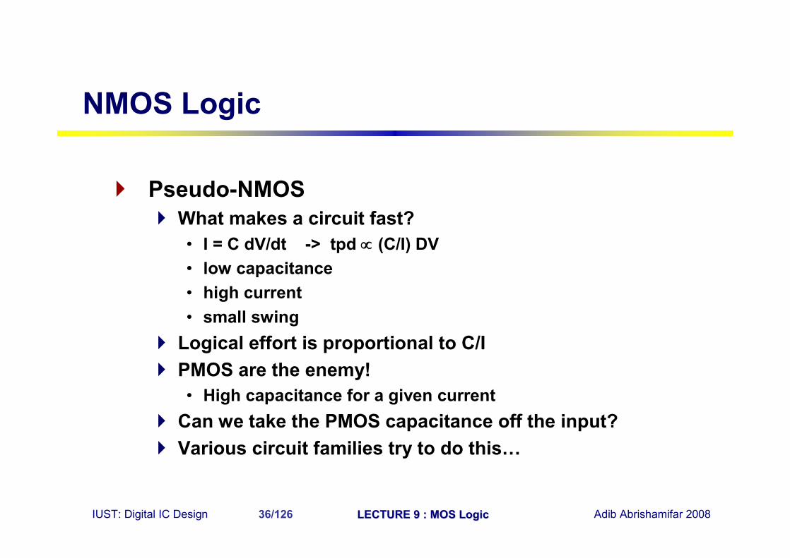
} Pseudo-NMOS} What makes a circuit fast?
• I = C dV/dt -> tpd ∝ (C/I) DV• low capacitance• high current• small swing
} Logical effort is proportional to C/I} PMOS are the enemy!
• High capacitance for a given current} Can we take the PMOS capacitance off the input?} Various circuit families try to do this…
NMOS Logic
IUST: Digital IC Design LECTURE 9 : MOS LogicLECTURE 9 : MOS Logic Adib Abrishamifar 200837/126
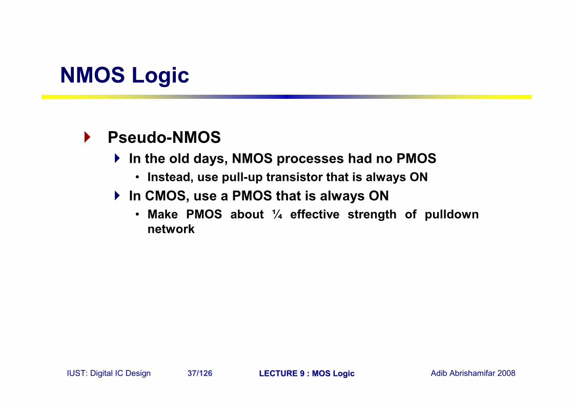
} Pseudo-NMOS} In the old days, NMOS processes had no PMOS
• Instead, use pull-up transistor that is always ON} In CMOS, use a PMOS that is always ON
• Make PMOS about ¼ effective strength of pulldown network
NMOS Logic

IUST: Digital IC Design LECTURE 9 : MOS LogicLECTURE 9 : MOS Logic Adib Abrishamifar 200838/126
} Pseudo-NMOS} Uses a p-type as a resistive pullup, n-type network for
pulldowns
NMOS Logic
Vi M1
Vdd+
VoM2

IUST: Digital IC Design LECTURE 9 : MOS LogicLECTURE 9 : MOS Logic Adib Abrishamifar 200839/126
} Pseudo-NMOS Characteristics} Compared to CMOS, this
family has higher packing density, since for n inputs only n+1 transistors are required
} The main disadvantages with Pseudo-NMOS Gates is the large static power dissipation that occurs whenever a pull-down path is activated
} Has much smaller pullupnetwork than static gate
} Pulldown time is longer because pullup is fighting
NMOS Logic
Vi M1
Vdd+
VoM2

IUST: Digital IC Design LECTURE 9 : MOS LogicLECTURE 9 : MOS Logic Adib Abrishamifar 200840/126
} Pseudo-NMOS Output Voltages} Logic 1 output is always at Vdd} Logic 0 output is above Vss} VOL = 0.25 (Vdd - Vss) is one
plausible choice
Vi M1
Vdd+
VoM2
NMOS Logic

IUST: Digital IC Design LECTURE 9 : MOS LogicLECTURE 9 : MOS Logic Adib Abrishamifar 200841/126
} Pseudo-NMOS Design Topics} For logic 0 output, pullup and
pulldown form a voltage divider} Must choose n, p transistor
sizes to create effective resistances of the required ratio
} Effective resistance of pulldown network must be computed in worst case—series n-types means larger transistors
Vi M1
Vdd+
VoM2
NMOS Logic

IUST: Digital IC Design LECTURE 9 : MOS LogicLECTURE 9 : MOS Logic Adib Abrishamifar 200842/126
} Pseudo-NMOS Transistor Ratio Calculation} In steady state logic 0 output ( for dual supply)
• pullup is in linear region• Vds = Vout - (Vdd or Vss)• pulldown is in saturation
} Pullup and pulldown have same current flowing through them
} Equate two currents• Idp = Idd
} Using 0.5 um parameters, 3.3V power supply• Wp/Lp / Wn/Ln = 3.9
} This is not suitable when use single supply!
NMOS Logic
Vi M1
Vdd+
VoM2
Vss−

IUST: Digital IC Design LECTURE 9 : MOS LogicLECTURE 9 : MOS Logic Adib Abrishamifar 200843/126
NMOS Logic
} Pseudo-NMOS Transistor Ratio Calculation} MOSFET sizing is important} Need to have reasonable W/L ratios for circuit to work
correctly} VOL>VSS but must be low enough to turn off/on next
MOSFET in the chain} Static current drain when “on”} Vout is a function of the number of parallel and series N
channels in the pull down network

IUST: Digital IC Design LECTURE 9 : MOS LogicLECTURE 9 : MOS Logic Adib Abrishamifar 200844/126
NMOS Logic
} Pseudo-NMOS Transistor Ratio Calculation} For single supply
( ) ( )OH
22OL P
n Tn OL TP
pOL n T 2
n
T Tn Tp
OL p n
V Vdd, For the worst case one NMOS to be on
V KK Vdd V V Vdd V
2 2
KV K (Vdd V ) 1 1
K
Assuming that V V V
V 0 K K
=
− − = −
= − − −
= =
→ ⇒ <<
A B C D
Vdd+
Y

IUST: Digital IC Design LECTURE 9 : MOS LogicLECTURE 9 : MOS Logic Adib Abrishamifar 200845/126
0.0 0.5 1.0 1.5 2.0 2.50.0
0.5
1.0
1.5
2.0
2.5
3.0
Vin [V]
Vou
t[V
]
W/Lp = 4
W/Lp = 2
W/Lp = 1
W/Lp = 0.25
W/Lp = 0.5
NMOS Logic
} Pseudo-NMOS VTC ( W/Ln=1)
IUST: Digital IC Design LECTURE 9 : MOS LogicLECTURE 9 : MOS Logic Adib Abrishamifar 200846/126
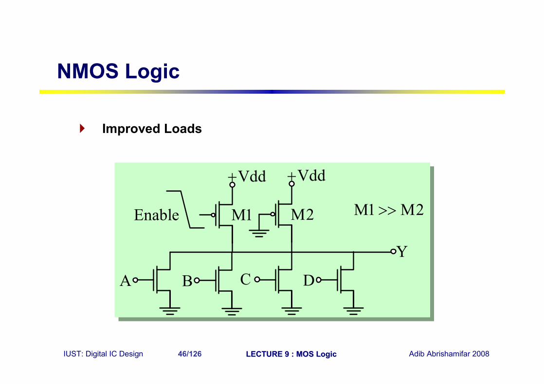
NMOS Logic
} Improved Loads
A B C D
Vdd+
Y
Vdd+
Enable M2M1 M1 M2>>

IUST: Digital IC Design LECTURE 9 : MOS LogicLECTURE 9 : MOS Logic Adib Abrishamifar 200847/126
} Pseudo-NMOS Gates} Design for unit current on output} PMOS fights NMOS
finputs
Y
NMOS Logic
IUST: Digital IC Design LECTURE 9 : MOS LogicLECTURE 9 : MOS Logic Adib Abrishamifar 200848/126
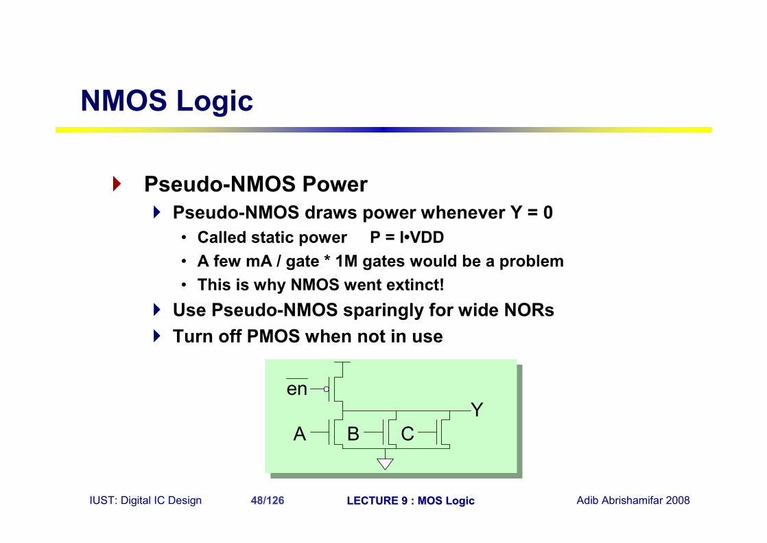
} Pseudo-NMOS Power} Pseudo-NMOS draws power whenever Y = 0
• Called static power P = I•VDD• A few mA / gate * 1M gates would be a problem• This is why NMOS went extinct!
} Use Pseudo-NMOS sparingly for wide NORs} Turn off PMOS when not in use
A BY
C
en
NMOS Logic

IUST: Digital IC Design LECTURE 9 : MOS LogicLECTURE 9 : MOS Logic Adib Abrishamifar 200849/126
Out
In1 In2 In3 In4
NMOS Logic
} Pseudo-NMOS ( NAND) Layout Example

IUST: Digital IC Design LECTURE 9 : MOS LogicLECTURE 9 : MOS Logic Adib Abrishamifar 200850/126
} Introduction} NMOS Logic
} Resistive Load } Saturated Enhancement Load} Linear Enhancement Load} Depletion Load} Some Gates} Transient in NMOS Circuit} Pseudo-NMOS
} CMOS Logic} Static CMOS Logic Gates
• NOT• NAND• NOR• Realization of More Complicated Gate Circuits
} Transmission Gates Family• NMOS Only Switch• CMOS
} Differential Cascode Voltage Switch Logic} Rules of Thumb
} Summary
Contents

IUST: Digital IC Design LECTURE 9 : MOS LogicLECTURE 9 : MOS Logic Adib Abrishamifar 200851/126
} Static CMOS Logic Family} All of the circuits described in the previous sections
have a large static power dissipation. This disadvantage can be overcome by using Static CMOS Logic Family
CMOS Logic

IUST: Digital IC Design LECTURE 9 : MOS LogicLECTURE 9 : MOS Logic Adib Abrishamifar 200852/126
} Introduction} NMOS Logic
} Resistive Load } Saturated Enhancement Load} Linear Enhancement Load} Depletion Load} Some Gates} Transient in NMOS Circuit} Pseudo-NMOS
} CMOS Logic} Static CMOS Logic Gates
• NOT• NAND• NOR• Realization of More Complicated Gate Circuits
} Transmission Gates Family• NMOS Only Switch• CMOS
} Differential Cascode Voltage Switch Logic} Rules of Thumb
} Summary
Contents

IUST: Digital IC Design LECTURE 9 : MOS LogicLECTURE 9 : MOS Logic Adib Abrishamifar 200853/126
Vi
M1
Vdd+
VoM2
CMOS Logic
} Static CMOS Logic Family} NOT

IUST: Digital IC Design LECTURE 9 : MOS LogicLECTURE 9 : MOS Logic Adib Abrishamifar 200854/126
CMOS Logic
} Static CMOS Logic Family} P/N ratio is normally selected for unit rise and fall resistance } Alternative: choose ratio for least average delay
• Only improves average delay slightly for inverters• But significantly decreases area and power
Vi
1
Vdd+
VoP
pdr
pd
pd
Least Delay
t K(P 1)
t K(P 1)( P)
t K (P 1)(1 P) 2
dt0
dPP 2 3
= +
= + µ
= + + µ
= ⇒
= µ ≈ −

IUST: Digital IC Design LECTURE 9 : MOS LogicLECTURE 9 : MOS Logic Adib Abrishamifar 200855/126
} Introduction} NMOS Logic
} Resistive Load } Saturated Enhancement Load} Linear Enhancement Load} Depletion Load} Some Gates} Transient in NMOS Circuit} Pseudo-NMOS
} CMOS Logic} Static CMOS Logic Gates
• NOT• NAND• NOR• Realization of More Complicated Gate Circuits
} Transmission Gates Family• NMOS Only Switch• CMOS
} Differential Cascode Voltage Switch Logic} Rules of Thumb
} Summary
Contents

IUST: Digital IC Design LECTURE 9 : MOS LogicLECTURE 9 : MOS Logic Adib Abrishamifar 200856/126
CMOS Logic
} Static CMOS Logic Family} Two inputs NAND
M3
B M2
YM4
Vdd+
A M1

IUST: Digital IC Design LECTURE 9 : MOS LogicLECTURE 9 : MOS Logic Adib Abrishamifar 200857/126
} Introduction} NMOS Logic
} Resistive Load } Saturated Enhancement Load} Linear Enhancement Load} Depletion Load} Some Gates} Transient in NMOS Circuit} Pseudo-NMOS
} CMOS Logic} Static CMOS Logic Gates
• NOT• NAND• NOR• Realization of More Complicated Gate Circuits
} Transmission Gates Family• NMOS Only Switch• CMOS
} Differential Cascode Voltage Switch Logic} Rules of Thumb
} Summary
Contents
IUST: Digital IC Design LECTURE 9 : MOS LogicLECTURE 9 : MOS Logic Adib Abrishamifar 200858/126
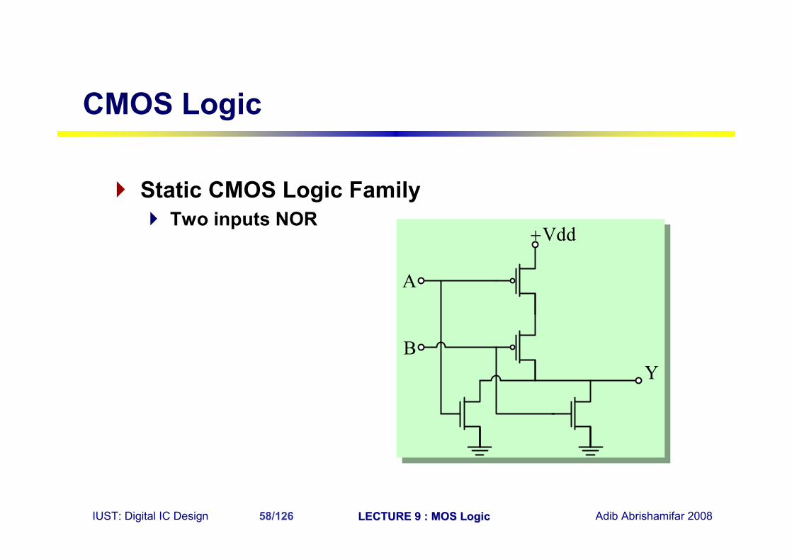
CMOS Logic
} Static CMOS Logic Family} Two inputs NOR
Y
A
B
Vdd+

IUST: Digital IC Design LECTURE 9 : MOS LogicLECTURE 9 : MOS Logic Adib Abrishamifar 200859/126
CMOS Logic
} Static CMOS Logic Family} NAND is more suitable for CMOS because by suppose
the equal W/L for NMOS and PMOS transistors, the PMOS transistor has more resistance respect to NMOS, therefore it is better to design circuit by paralleling the PMOS and cascading the NMOS
} The better Technology for digital circuit is N-Well, because in this Technology the NMOS transistors are made in the Sub. Which result better characteristic for transistor

IUST: Digital IC Design LECTURE 9 : MOS LogicLECTURE 9 : MOS Logic Adib Abrishamifar 200860/126
} Introduction} NMOS Logic
} Resistive Load } Saturated Enhancement Load} Linear Enhancement Load} Depletion Load} Some Gates} Transient in NMOS Circuit} Pseudo-NMOS
} CMOS Logic} Static CMOS Logic Gates
• NOT• NAND• NOR• Realization of More Complicated Gate Circuits
} Transmission Gates Family• NMOS Only Switch• CMOS
} Differential Cascode Voltage Switch Logic} Rules of Thumb
} Summary
Contents

IUST: Digital IC Design LECTURE 9 : MOS LogicLECTURE 9 : MOS Logic Adib Abrishamifar 200861/126
} Realization of More Complicated Gate Circuits} a) Y = A(B+C)} It can be implemented in three levels:
• Gate Level• Transistor Level• Layout Level
CMOS Logic

IUST: Digital IC Design LECTURE 9 : MOS LogicLECTURE 9 : MOS Logic Adib Abrishamifar 200862/126
} Realization of More Complicated Gate Circuits} a) Y = A(B+C)
• Gate Level– It consists of 10 transistors, 4 transistors for NOR, 2 for NOT and 4 for
NAND
AYB
C
CMOS Logic

IUST: Digital IC Design LECTURE 9 : MOS LogicLECTURE 9 : MOS Logic Adib Abrishamifar 200863/126
} Realization of More Complicated Gate Circuits} a) Y = A(B+C)
• Transistor Level– It need only 6 transistors
A
B
C
Vdd+
Y
A
B C
CMOS Logic

IUST: Digital IC Design LECTURE 9 : MOS LogicLECTURE 9 : MOS Logic Adib Abrishamifar 200864/126
} Realization of More Complicated Gate Circuits} a) Y = A(B+C)
• Layout Level– By proper construction of layout, the parasitic capacitors are also
reduced and area can be saved
CMOS Logic

IUST: Digital IC Design LECTURE 9 : MOS LogicLECTURE 9 : MOS Logic Adib Abrishamifar 200865/126
} Realization of More Complicated Gate Circuits} b) XNOR (Y = AB + AB)
• Gate Level– 16 transistors are needed
A
B
Y
CMOS Logic

IUST: Digital IC Design LECTURE 9 : MOS LogicLECTURE 9 : MOS Logic Adib Abrishamifar 200866/126
} Realization of More Complicated Gate Circuits} b) XNOR (Y = AB + AB)
• Transistor Level (1)» How many transistors are» needed?
Vdd+
A
A
A
A
B
BB
B
Y AB AB= +
CMOS Logic

IUST: Digital IC Design LECTURE 9 : MOS LogicLECTURE 9 : MOS Logic Adib Abrishamifar 200867/126
} Realization of More Complicated Gate Circuits} b) XNOR
• Transistor Level (2)– Previous circuit can be
simplified by eliminatingtwo wiring lines
Vdd+
A
A
A
A
B
BB
B
Y AB AB= +
CMOS Logic

IUST: Digital IC Design LECTURE 9 : MOS LogicLECTURE 9 : MOS Logic Adib Abrishamifar 200868/126
} Realization of More Complicated Gate Circuits} b) XNOR
• Transistor Level (3)– In this circuit we have
static power dissipationin the state of (A=0,B=1)or (A=1,B=0)
A
M1
Vdd+
M3Y AB AB= +
M2
B
CMOS Logic
IUST: Digital IC Design LECTURE 9 : MOS LogicLECTURE 9 : MOS Logic Adib Abrishamifar 200869/126
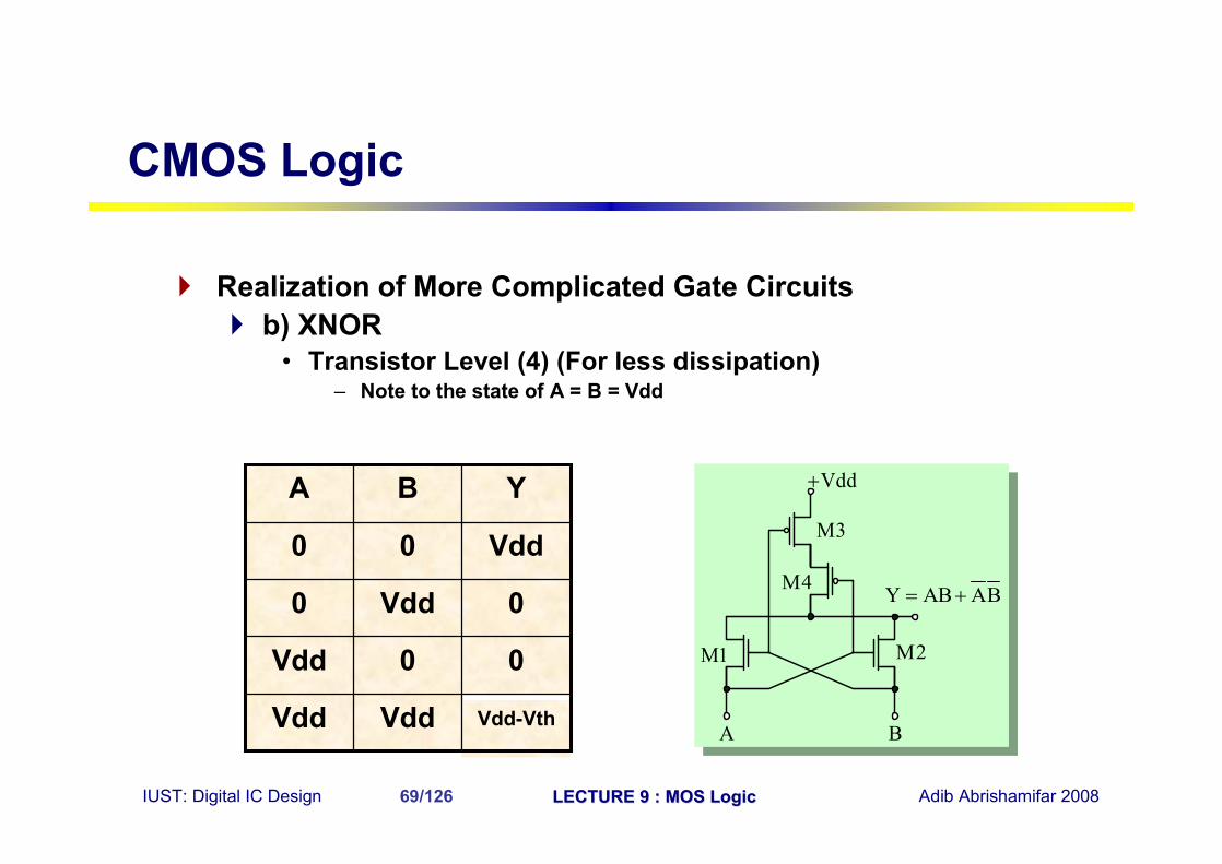
} Realization of More Complicated Gate Circuits} b) XNOR
• Transistor Level (4) (For less dissipation)– Note to the state of A = B = Vdd
A
M1
Vdd+
M3
Y AB AB= +
M2
B
M4
Vdd-VthVddVdd
00Vdd
0Vdd0
Vdd00
YBA
CMOS Logic

IUST: Digital IC Design LECTURE 9 : MOS LogicLECTURE 9 : MOS Logic Adib Abrishamifar 200870/126
} Realization of More Complicated Gate Circuits} c) XOR
• As Previous the Source and Drain of M3 (or M4) are replaced by each other in different states, for example in state of A=0, B=0 the b connection of M3 is Source
0VddVdd
Vdd0Vdd
Vdd-VthVdd0
Vth00
YBA Vdd+
A B
M1
M2 M3
M4
Y AB AB= +
A
a
ab
b
CMOS Logic

IUST: Digital IC Design LECTURE 9 : MOS LogicLECTURE 9 : MOS Logic Adib Abrishamifar 200871/126
} Realization of More Complicated Gate Circuits} d) Tri-State Outputs
• A floating state at the output is needed– Non-Inverting
D
En
Y
D
Vdd+En
Y
En 1 Y DEn 0 Y Hi Z
= ⇒ = = ⇒ = −
CMOS Logic

IUST: Digital IC Design LECTURE 9 : MOS LogicLECTURE 9 : MOS Logic Adib Abrishamifar 200872/126
} Realization of More Complicated Gate Circuits} d) Tri-State Outputs
• A floating state at the output is needed– Inverting
En 1 Y Hi Z
En 0 Y D
= ⇒ = −
= ⇒ =
D
En
Y
Vdd+
D
En
Y
CMOS Logic

IUST: Digital IC Design LECTURE 9 : MOS LogicLECTURE 9 : MOS Logic Adib Abrishamifar 200873/126
} Realization of More Complicated Gate Circuits} e) Schmitt Trigger
• M3 and M6 have minimum sized geometries
• With Vin = 0 , the transistors M1 and M2 will be on but conducting negligible Drain current since M4 and M5 are off
Vdd+
Vin Y
Vdd+
M5M6Vz
M4
VyM2
M3M1
Vx
TN
Vy Vx VddVy Vdd M6 on Vz Vy V⇒ ≈ ≈
≈ ⇒ ≅ ⇒ = −
CMOS Logic

IUST: Digital IC Design LECTURE 9 : MOS LogicLECTURE 9 : MOS Logic Adib Abrishamifar 200874/126
} Realization of More Complicated Gate Circuits} e) Schmitt Trigger
• When Vin rise to VTN, M5 turns on, but M4 is off. M5 and M6 form an NMOS amplifier. Thus as Vin rises, Vz is falling and in the certain voltage M4 turns on. With both M4 and M5 conducting, Vy rapidly goes to zero turning off M6. With Vy=0, M3 turns on, which aids in turning off M2 as Vx goes from Vdd to Vy-VTP
• As Vin decrease from Vdd to zero the operation is essentially similar. But now M1 turns on, in different voltage and …
Vdd+
Vin Y
Vdd+
M5M6Vz
M4
VyM2
M3M1
Vx
CMOS Logic

IUST: Digital IC Design LECTURE 9 : MOS LogicLECTURE 9 : MOS Logic Adib Abrishamifar 200875/126
} Introduction} NMOS Logic
} Resistive Load } Saturated Enhancement Load} Linear Enhancement Load} Depletion Load} Some Gates} Transient in NMOS Circuit} Pseudo-NMOS
} CMOS Logic} Static CMOS Logic Gates
• NOT• NAND• NOR• Realization of More Complicated Gate Circuits
} Transmission Gates Family• NMOS Only Switch• CMOS
} Differential Cascode Voltage Switch Logic} Rules of Thumb
} Summary
Contents

IUST: Digital IC Design LECTURE 9 : MOS LogicLECTURE 9 : MOS Logic Adib Abrishamifar 200876/126
} Transmission Gates Family} Use pass transistors like switches to do logic} Inputs drive diffusion terminals as well as gates} N transistors instead of 2N} No static power consumption} Ratioless} Bidirectional
CMOS Logic

IUST: Digital IC Design LECTURE 9 : MOS LogicLECTURE 9 : MOS Logic Adib Abrishamifar 200877/126
} Introduction} NMOS Logic
} Resistive Load } Saturated Enhancement Load} Linear Enhancement Load} Depletion Load} Some Gates} Transient in NMOS Circuit} Pseudo-NMOS
} CMOS Logic} Static CMOS Logic Gates
• NOT• NAND• NOR• Realization of More Complicated Gate Circuits
} Transmission Gates Family• NMOS Only Switch• CMOS
} Differential Cascode Voltage Switch Logic} Rules of Thumb
} Summary
Contents
IUST: Digital IC Design LECTURE 9 : MOS LogicLECTURE 9 : MOS Logic Adib Abrishamifar 200878/126
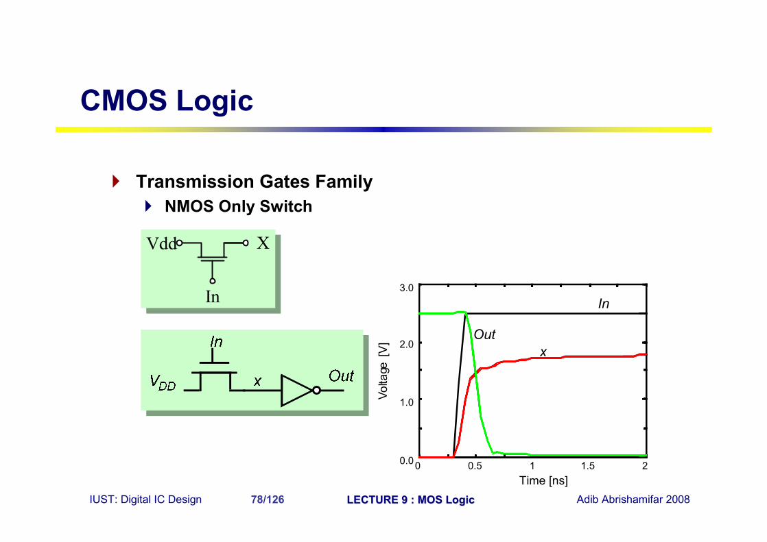
} Transmission Gates Family} NMOS Only Switch
CMOS Logic
0 0.5 1 1.5 20.0
1.0
2.0
3.0
Time [ns]
Vol ta
ge[V
]
xOut
In
Vdd X
In

IUST: Digital IC Design LECTURE 9 : MOS LogicLECTURE 9 : MOS Logic Adib Abrishamifar 200879/126
} Transmission Gates Family} NMOS Only Switch
• VB does not pull up to 2.5V, but 2.5-VTN
• Threshold voltage loss causes (M2 may be weakly conducting forming a path from Vdd to GND)
• NMOS has higher threshold than PMOS (body effect)
CMOS Logic

IUST: Digital IC Design LECTURE 9 : MOS LogicLECTURE 9 : MOS Logic Adib Abrishamifar 200880/126
CMOS Logic
} Transmission Gates Family} NMOS Only Switch
• Pass transistor gates should never be cascaded as on the left
• Logic on the right suffers from static power dissipation and reduced noise margins

IUST: Digital IC Design LECTURE 9 : MOS LogicLECTURE 9 : MOS Logic Adib Abrishamifar 200881/126
} Transmission Gates Family} NMOS Only Switch
• Solution1: Level Restoring Transistor
CMOS Logic
M2
M1
n OutA
B
VVdd
XM
M
Mr
OutA
B
VddV
Level Restorer
X

IUST: Digital IC Design LECTURE 9 : MOS LogicLECTURE 9 : MOS Logic Adib Abrishamifar 200882/126
} Transmission Gates Family} NMOS Only Switch
• Solution1: Level Restoring Transistor} Advantages
• Full swing on x (due to Level Restorer) so no static power consumption by inverter
• No static backward current path through Level Restorer and PT since Restorer is only active when A is high
• Restorer adds capacitance, takes away pull down current at X} For correct operation Mr must be sized correctly (ratioed)
CMOS Logic

IUST: Digital IC Design LECTURE 9 : MOS LogicLECTURE 9 : MOS Logic Adib Abrishamifar 200883/126
} Transmission Gates Family} NMOS Only Switch
• Solution2: Multiple VT Transistors
CMOS Logic

IUST: Digital IC Design LECTURE 9 : MOS LogicLECTURE 9 : MOS Logic Adib Abrishamifar 200884/126
} Transmission Gates Family} NMOS Only Switch
• Solution2: Multiple VT Transistors} Technology solution: Use (near) zero VT devices for the
NMOS TGs to eliminate most of the threshold drop (body effect still in force preventing full swing to Vdd)
} Impacts static power consumption due to subthresholdcurrents flowing through the TGs (even if VGS is below VT)
CMOS Logic
Out
In2 = 0V
In1 = 2.5V
A = 2.5V
B = 0V
low VT transistors
sneak path
on
off but leaking

IUST: Digital IC Design LECTURE 9 : MOS LogicLECTURE 9 : MOS Logic Adib Abrishamifar 200885/126
} Transmission Gates Family} NMOS Only Switch
• Disadvantage:– It can be bad because the signal can be degraded– We do not allow a few gates in series for one signal (Pure TG logic
is not regenerative, the signal gradually degrades after passing through a number of TGs)
• Advantage:– Allow us to save transistor or less stage of logic
CMOS Logic

IUST: Digital IC Design LECTURE 9 : MOS LogicLECTURE 9 : MOS Logic Adib Abrishamifar 200886/126
} Introduction} NMOS Logic
} Resistive Load } Saturated Enhancement Load} Linear Enhancement Load} Depletion Load} Some Gates} Transient in NMOS Circuit} Pseudo-NMOS
} CMOS Logic} Static CMOS Logic Gates
• NOT• NAND• NOR• Realization of More Complicated Gate Circuits
} Transmission Gates Family• NMOS Only Switch• CMOS
} Differential Cascode Voltage Switch Logic} Rules of Thumb
} Summary
Contents

IUST: Digital IC Design LECTURE 9 : MOS LogicLECTURE 9 : MOS Logic Adib Abrishamifar 200887/126
} CMOS Transmission Gates Family} PMOS
} CMOS
A Y
C
CMOS Logic
C
C
A Y A Y
C
C
IUST: Digital IC Design LECTURE 9 : MOS LogicLECTURE 9 : MOS Logic Adib Abrishamifar 200888/126
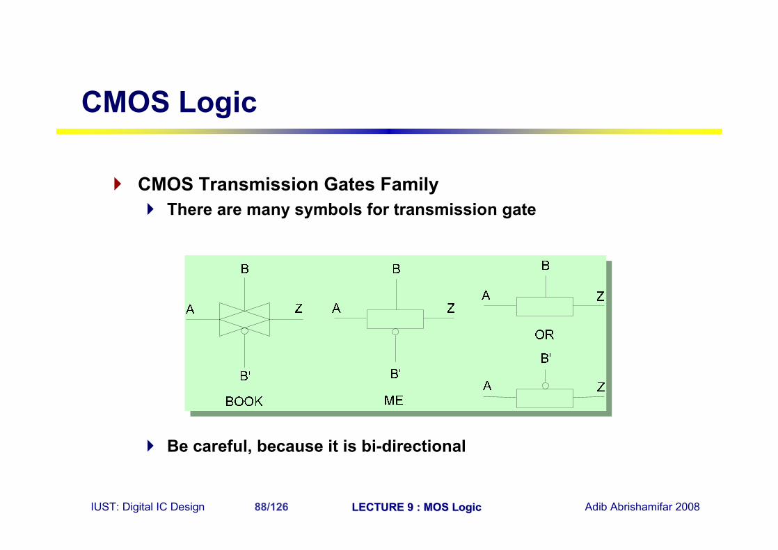
} CMOS Transmission Gates Family} There are many symbols for transmission gate
} Be careful, because it is bi-directional
CMOS Logic

IUST: Digital IC Design LECTURE 9 : MOS LogicLECTURE 9 : MOS Logic Adib Abrishamifar 200889/126
} CMOS Transmission Gates Family} This circuit performs a function similar to that of the well known diode bridge
} The input voltage VA (which must be between Vss and Vdd) is then connected to the output through the parallel on resistance of the channels of the two transistors. As VA approaches Vdd, the N-channel device cuts off but the P-channel device remains non saturated, as VA approaches Vss, the P-channel device cuts off but the N-channel device remains non saturated. Therefore there is always a non saturated transistor between input and output
CMOS Logic
C
C
A Y A Y
C
C
C Vss, C 0 Both transistor are on A Y= = ⇒ ⇒ =

IUST: Digital IC Design LECTURE 9 : MOS LogicLECTURE 9 : MOS Logic Adib Abrishamifar 200890/126
C
C
A YCL
PI
NI
S
D
t
VA
Vdd
Vy
} CMOS Transmission Gates Family} For more understanding note to this circuit} We assume:
CMOS Logic
TP TNVy(0 ) 0, C Vdd, C 0, V Vdd V− = = = < −

IUST: Digital IC Design LECTURE 9 : MOS LogicLECTURE 9 : MOS Logic Adib Abrishamifar 200891/126
C
C
A YCL
PI
NI
} CMOS Transmission Gates Family
CMOS Logic
TP
TP TN
TN
CL N PVy V
PVy V Vy Vdd V
PVy Vdd V Vy Vdd
N sat0 t t I I I
P sat
N satt t t r CL
P triode
N offt t t r CL
P triode
=
= = −
= − =
=≤ ≤ ⇒ ⇒ = + =
=≤ ≤ ⇒ ⇒ τ ≈ =
=≤ ≤ ⇒ ⇒ τ ≈ =

IUST: Digital IC Design LECTURE 9 : MOS LogicLECTURE 9 : MOS Logic Adib Abrishamifar 200892/126
C
C
A YCL
PI
NI
} CMOS Transmission Gates Family} It is normally assumed as a resistor
CMOS Logic
A
TG
TG TG
TG N P
V (t) Vddu(t)
tVy(t) Vdd 1 exp u(t)
R CLR r r
=
−= −
τ τ =
=

IUST: Digital IC Design LECTURE 9 : MOS LogicLECTURE 9 : MOS Logic Adib Abrishamifar 200893/126
} CMOS Transmission Gates Family} rN and rP are approximately as follow (In saturation region)
ANN 2
N TN
APP 2
P TP
A
2Vr
(Vdd V )2V
r(Vdd V )
V is Early Voltage
≈β −
≈β −
CMOS Logic
R
VyTPV TNVdd V− Vdd
Pr Nr
TG N PR r r=

IUST: Digital IC Design LECTURE 9 : MOS LogicLECTURE 9 : MOS Logic Adib Abrishamifar 200894/126
} CMOS Transmission Gates Family} What to note about TG
• The inputs must be able to give high current because they are connected directly to Drain and Source of transistors
• Since each input is connected to an RC circuit, The delay can be considered directly
• Limited Fan-in• Excessive Fan-out• Noise vulnerability (not restoring)• Supply voltage offset/bias vulnerability• Poor high voltage levels if NMOS-only• Body effect
CMOS Logic
IUST: Digital IC Design LECTURE 9 : MOS LogicLECTURE 9 : MOS Logic Adib Abrishamifar 200895/126
} CMOS Transmission Gates Family } Rules of Thumb
• Pass-Logic may consume half the power of static logic. But be careful of VT drop resulting in static leakage
• Pass-Gate Logic is not appropriate when long interconnects separate logic stages or when circuits have high Fan-out load (use buffering)
CMOS Logic

IUST: Digital IC Design LECTURE 9 : MOS LogicLECTURE 9 : MOS Logic Adib Abrishamifar 200896/126
} CMOS Transmission Gates Family} AND
CMOS Logic

IUST: Digital IC Design LECTURE 9 : MOS LogicLECTURE 9 : MOS Logic Adib Abrishamifar 200897/126
} CMOS Transmission Gates Family} OR
Y A AB (A A)(A B) A B= + = + + = +
CMOS Logic
A
Y
A
BAB
A
A
Wired OR
IUST: Digital IC Design LECTURE 9 : MOS LogicLECTURE 9 : MOS Logic Adib Abrishamifar 200898/126
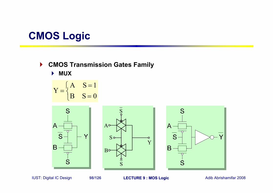
} CMOS Transmission Gates Family} MUX
A S 1Y
B S 0=
= =
CMOS Logic
A
Y
S
B
S
S

IUST: Digital IC Design LECTURE 9 : MOS LogicLECTURE 9 : MOS Logic Adib Abrishamifar 200899/126
} CMOS Transmission Gates Family} MUX
CMOS Logic
GND
Vdd
In1 In2S S
S S F
1 2F (In S In S)= +

IUST: Digital IC Design LECTURE 9 : MOS LogicLECTURE 9 : MOS Logic Adib Abrishamifar 2008100/126
} CMOS Transmission Gates Family} XOR
CMOS Logic
A
Y A B= ⊕
B
B
B
IUST: Digital IC Design LECTURE 9 : MOS LogicLECTURE 9 : MOS Logic Adib Abrishamifar 2008101/126
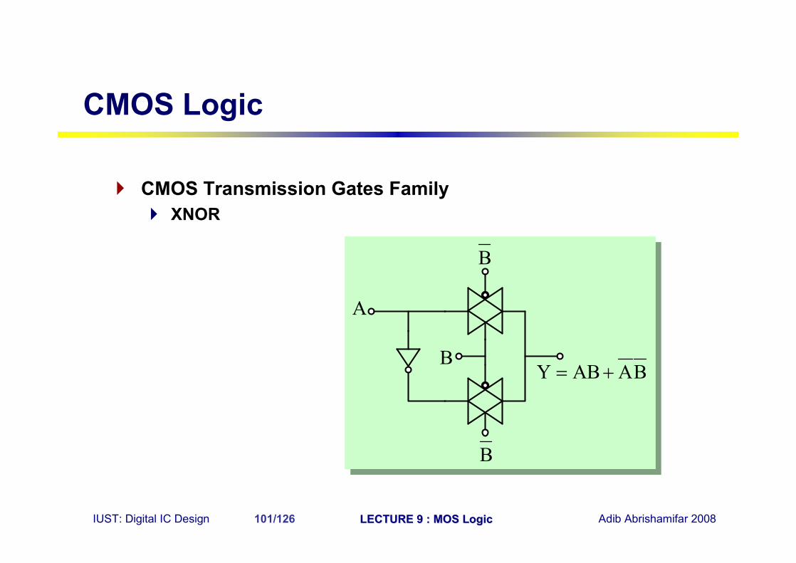
} CMOS Transmission Gates Family} XNOR
CMOS Logic
A
Y AB AB= +B
B
B
IUST: Digital IC Design LECTURE 9 : MOS LogicLECTURE 9 : MOS Logic Adib Abrishamifar 2008102/126
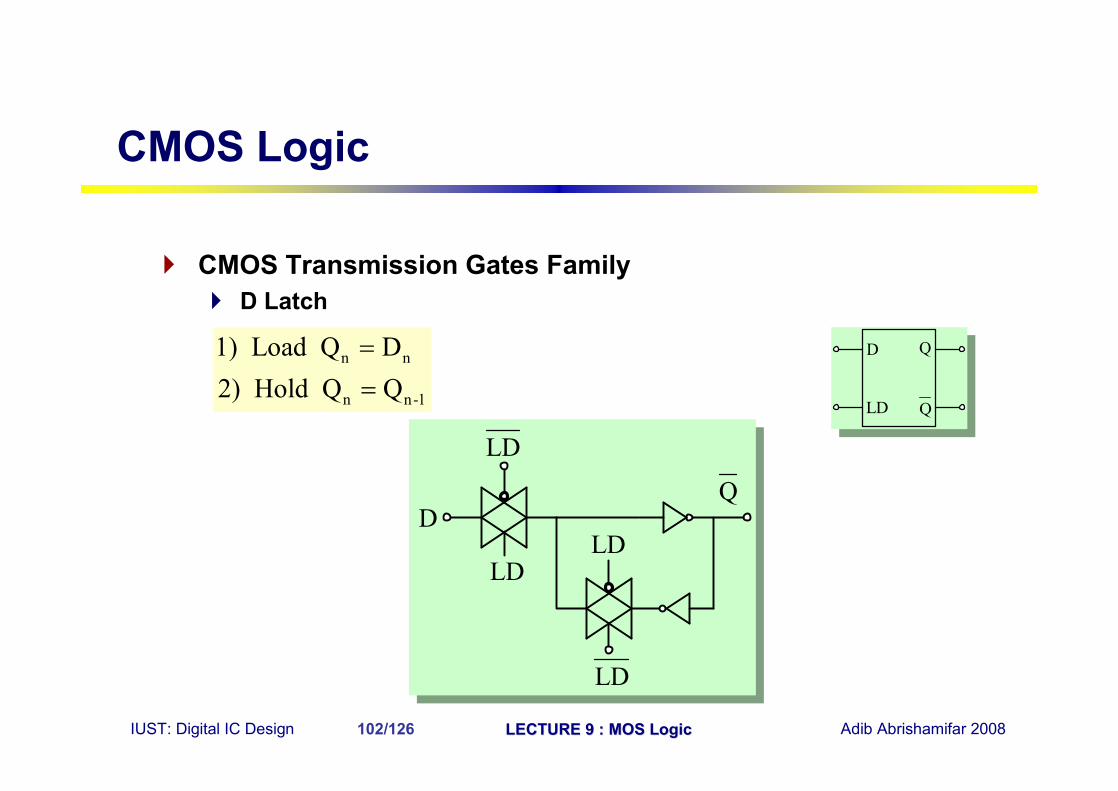
} CMOS Transmission Gates Family} D Latch
CMOS Logic
D
LD
Q
Q
n n
n n-1
1) Load Q D2) Hold Q Q
==
DQ
LD
LD
LDLD

IUST: Digital IC Design LECTURE 9 : MOS LogicLECTURE 9 : MOS Logic Adib Abrishamifar 2008103/126
} CMOS Transmission Gates Family} D Latch
CMOS Logic
1) Load LD 1=
2) Hold LD 0=
D Q D=
D Q=
Q
Q

IUST: Digital IC Design LECTURE 9 : MOS LogicLECTURE 9 : MOS Logic Adib Abrishamifar 2008104/126
} CMOS Transmission Gates Family} D Latch (Simpler Realization)
• If in Load Mode a level voltage opposite to the output of weak inverter is applied to the input by TG, Q = D and weak inverter is not damaged!
CMOS Logic
DQ
LD
LD
QWeak Inverter

IUST: Digital IC Design LECTURE 9 : MOS LogicLECTURE 9 : MOS Logic Adib Abrishamifar 2008105/126
C C C C C C
e qR e qR e qR eqR e qR e qRIn
m
C C C C C C
e qR e qR e qR e qR eqR e qRIn 1V 2V iV i 1V + n 1V − nV
C C C C C CIn 1V 2V iV i 1V + n 1V − nV
CMOS Logic
} Delay in Transmission Gate
IUST: Digital IC Design LECTURE 9 : MOS LogicLECTURE 9 : MOS Logic Adib Abrishamifar 2008106/126
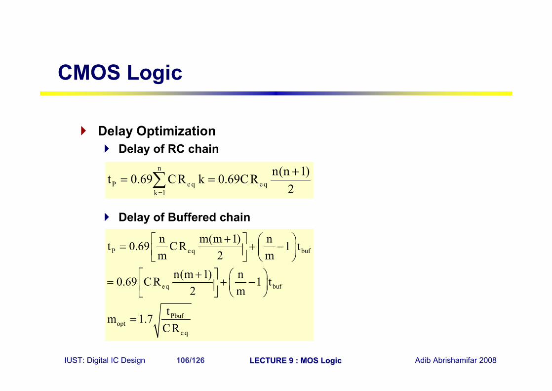
} Delay Optimization} Delay of RC chain
} Delay of Buffered chain
n
P e q e qk 1
n(n 1)t 0.69 C R k 0.69C R2=
+= =∑
CMOS Logic
P eq buf
eq buf
Pbufopt
e q
n m(m 1) nt 0.69 C R 1 tm 2 m
n(m 1) n0.69 C R 1 t2 m
tm 1.7
C R
+ = + − + = + −
=

IUST: Digital IC Design LECTURE 9 : MOS LogicLECTURE 9 : MOS Logic Adib Abrishamifar 2008107/126
CMOS Logic
} TG Points to Remember} Stored charge leaks away due to reverse-bias leakage
current} Stored value is good for about 1 ms} Value must be rewritten to be valid} If not loaded every cycle, must ensure that latch is
loaded often enough to keep data valid} Capacitance comes primarily from inverter’s gate logic

IUST: Digital IC Design LECTURE 9 : MOS LogicLECTURE 9 : MOS Logic Adib Abrishamifar 2008108/126
CMOS Logic
} TG Layout

IUST: Digital IC Design LECTURE 9 : MOS LogicLECTURE 9 : MOS Logic Adib Abrishamifar 2008109/126
CMOS Logic
} TG Properties} Strong pull-up} Strong pull-down} May be difficult to design into a circuit (layout) because
of close proximity of N and P devices (design rule separation)
} Always requires 2N transisitors for any N x TG design} Many logic functions (multiplexers in particular) are
easily implemented using TG based designs

IUST: Digital IC Design LECTURE 9 : MOS LogicLECTURE 9 : MOS Logic Adib Abrishamifar 2008110/126
} Complementary Pass-transistor Logic (CPL) or Differential (+) TG Logic} Dual-rail form of pass transistor logic} Avoids need for ratioed feedback
B
S
S
S
S
A
B
AY
YL
L
CMOS Logic
A
B
AB
PT Network F
A
B
AB
Inverse PT Network F
F
F

IUST: Digital IC Design LECTURE 9 : MOS LogicLECTURE 9 : MOS Logic Adib Abrishamifar 2008111/126
CMOS Logic
} CPL
A
A F=A B
F=A B
BB
XOR/XNOR
A
A
A
AA F=A B
F=A B
BBB
XOR/XNOR
AA
AF=AB+B
A
A
B
B
B B
AND/NAND
A
A
B
B
B B
AND/NAND
A
A
BF=AB+BB
BB
B BB
AND/NAND
F=AB
F=AB

IUST: Digital IC Design LECTURE 9 : MOS LogicLECTURE 9 : MOS Logic Adib Abrishamifar 2008112/126
CMOS Logic
} 4 Input NAND in CPL
OUT
X
X
YOUT
Y Y
Y

IUST: Digital IC Design LECTURE 9 : MOS LogicLECTURE 9 : MOS Logic Adib Abrishamifar 2008113/126
CMOS Logic
} CPL Advantages} Differential so complementary data inputs and outputs
are always available (so don’t need extra inverters)} Still static, since the output defining nodes are always
tied to Vdd or GND through a low resistance path} Design is modular, all gates use the same topology,
only the inputs are permuted} Simple XOR makes it attractive for structures like
adders} Fast (assuming number of transistors in series is small)

IUST: Digital IC Design LECTURE 9 : MOS LogicLECTURE 9 : MOS Logic Adib Abrishamifar 2008114/126
CMOS Logic
} CPL Disadvantages} Additional routing overhead for complementary signals} Still have static power dissipation problems} VOH is very weak! Then we need an inverter at the
output

IUST: Digital IC Design LECTURE 9 : MOS LogicLECTURE 9 : MOS Logic Adib Abrishamifar 2008115/126
} Introduction} NMOS Logic
} Resistive Load } Saturated Enhancement Load} Linear Enhancement Load} Depletion Load} Some Gates} Transient in NMOS Circuit} Pseudo-NMOS
} CMOS Logic} Static CMOS Logic Gates
• NOT• NAND• NOR• Realization of More Complicated Gate Circuits
} Transmission Gates Family• NMOS Only Switch• CMOS
} Differential Cascode Voltage Switch Logic} Rules of Thumb
} Summary
Contents
IUST: Digital IC Design LECTURE 9 : MOS LogicLECTURE 9 : MOS Logic Adib Abrishamifar 2008116/126
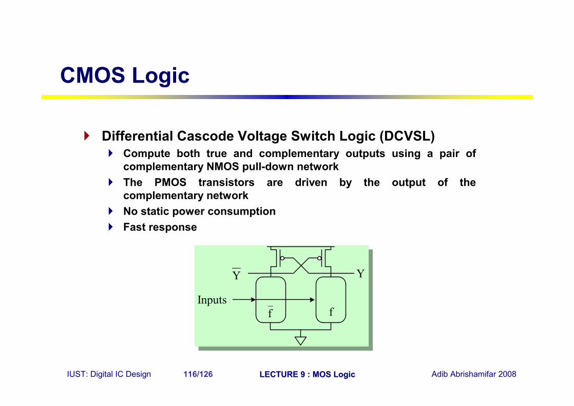
} Differential Cascode Voltage Switch Logic (DCVSL)} Compute both true and complementary outputs using a pair of
complementary NMOS pull-down network} The PMOS transistors are driven by the output of the
complementary network} No static power consumption} Fast response
CMOS Logic
Inputs
Y Y
f f

IUST: Digital IC Design LECTURE 9 : MOS LogicLECTURE 9 : MOS Logic Adib Abrishamifar 2008117/126
} Differential Cascode Voltage Switch Logic (DCVSL)} Example: NAND/AND
CMOS Logic
Y AB=
BA
A
B
Y A B= +
Series
IUST: Digital IC Design LECTURE 9 : MOS LogicLECTURE 9 : MOS Logic Adib Abrishamifar 2008118/126
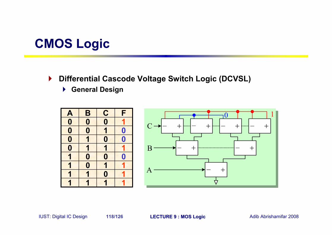
} Differential Cascode Voltage Switch Logic (DCVSL)} General Design
11111011110100011110001001001000FCBA
CMOS Logic
+ + + +
++
+
_ _ _ _
__
_A
B
C0 1

IUST: Digital IC Design LECTURE 9 : MOS LogicLECTURE 9 : MOS Logic Adib Abrishamifar 2008119/126
} Differential Cascode Voltage Switch Logic (DCVSL)} General Design
+_x
a b
u
x x
a b
uu ax bx= +
≡
CMOS Logic
+_x
u
≡
u
+_x
a b
1u
+_
a b
2u
+_x
a b
1u
≡
2u

IUST: Digital IC Design LECTURE 9 : MOS LogicLECTURE 9 : MOS Logic Adib Abrishamifar 2008120/126
} Differential Cascode Voltage Switch Logic (DCVSL)} General Design
+ + + +
++
+
_ _ _ _
__
_A
B
C0 1
CMOS Logic
+ +
++
+
_ _
__
_A
B
C
0 1

IUST: Digital IC Design LECTURE 9 : MOS LogicLECTURE 9 : MOS Logic Adib Abrishamifar 2008121/126
C
B
A AB B
B
CC C
o1
CMOS Logic
} Differential Cascode Voltage Switch Logic (DCVSL)} General Design

IUST: Digital IC Design LECTURE 9 : MOS LogicLECTURE 9 : MOS Logic Adib Abrishamifar 2008122/126
} Differential Cascode Voltage Switch Logic (DCVSL)} Example: XOR/XNOR
CMOS Logic

IUST: Digital IC Design LECTURE 9 : MOS LogicLECTURE 9 : MOS Logic Adib Abrishamifar 2008123/126
} Introduction} NMOS Logic
} Resistive Load } Saturated Enhancement Load} Linear Enhancement Load} Depletion Load} Some Gates} Transient in NMOS Circuit} Pseudo-NMOS
} CMOS Logic} Static CMOS Logic Gates
• NOT• NAND• NOR• Realization of More Complicated Gate Circuits
} Transmission Gates Family• NMOS Only Switch• CMOS
} Differential Cascode Voltage Switch Logic} Rules of Thumb
} Summary
Contents

IUST: Digital IC Design LECTURE 9 : MOS LogicLECTURE 9 : MOS Logic Adib Abrishamifar 2008124/126
} Rules of Thumb} Step-up (alpha) ratio of 2.7 (“e”) produces minimum power-
delay product} P vs. N (beta) ratio of 2 balances pull-up and pull-down
times and noise margins} Approximately 75% of static logic are NAND stacks (limit
stack to 3-4, use ordering and tapering for speed)} Glitches consume approximately 15% of overall chip power} Crossover (short-circuit) current consumes ~ 10% of a
static chip’s total power (but is a function of input/output slews, ie sizing)
CMOS Logic

IUST: Digital IC Design LECTURE 9 : MOS LogicLECTURE 9 : MOS Logic Adib Abrishamifar 2008125/126
} Introduction} NMOS Logic
} Resistive Load } Saturated Enhancement Load} Linear Enhancement Load} Depletion Load} Some Gates} Transient in NMOS Circuit} Pseudo-NMOS
} CMOS Logic} Static CMOS Logic Gates
• NOT• NAND• NOR• Realization of More Complicated Gate Circuits
} Transmission Gates Family• NMOS Only Switch• CMOS
} Differential Cascode Voltage Switch Logic} Rules of Thumb
} Summary
Contents

IUST: Digital IC Design LECTURE 9 : MOS LogicLECTURE 9 : MOS Logic Adib Abrishamifar 2008126/126
Summary
} This lecture describes the basic MOS Logic Gates which require no clock or other periodic signal for operation and also implementation of them in three following levels} Gate Level} Transistor level} Layout Level