andescore n1213-s
TRANSCRIPT

www.andestech.com1
AndesCore N1213-SAndesCore N1213-S

Page 2
AndesCore™ N1213-S AndesCore™ N1213-S
CPU Core32bit CPU Single issue with 8-stage pipelineAndeStar™ ISA with 16-/32-bit intermixable instructions to reduce code sizeDynamic branch prediction to reduce branch penalties• 32/64/128/256 BTB
Configurability for customersConfiguration options for power, performance and area requirements

Page 3
AndesCore™ N1213-S AndesCore™ N1213-S
MMUfully-associative iTLB/dTLB: 4 or 8 entries4-way set-associative main TLB: 32/64/128 entriesTwo groups of pages size support: (4K,1M) and (8K,1M)Locking support for TLB
I & D cacheVirtual index and physical tag (for faster context switching)Cache size: 8KB/16KB/32KB/64KBCache line size: 16B/32B2/4-way set associativeI Cache locking support

Page 4
AndesCore™ N1213-S AndesCore™ N1213-S
I & D Local memorywide range support for internal /external local memory
• 4KB~1024KB Provide fixed access latencies for internal local memoryDouble buffer mode for D local memoryOptional external local memory interface
BusSynchronous/Asynchronous AHB
• 1 or 2 port configurationSynchronous HSMP
• AXI like• 1 or 2 port configuration

Page 5
AndesCore™ N1213-SAndesCore™ N1213-S
For performanceImproved memory accesses:
• 1D/2D DMA, load/store multipleEfficient synchronization without locking the whole bus
• Load lock, store conditional instructionsVectored interrupt to improve real-time performance
• 6 interrupt signalsMMU
• Optional HW page table walker• TLB management instructions
For flexibilityMemory-mapped IO spacePC-relative jumps for position independent codeJTAG-based debug supportOptional embedded program trace interfacePerformance monitors for performance tuning Bi-endian modes to support flexible data input
Page 6
AndesCore™ N1213-S OverviewAndesCore™ N1213-S Overview
For power ManagementClock-gated pipelineLow-power mode support instructionsRedundant memory access reductionMany CPU/bus frequency ratio support
Page 7
Cache SRAM example – 32KBCache SRAM example – 32KB
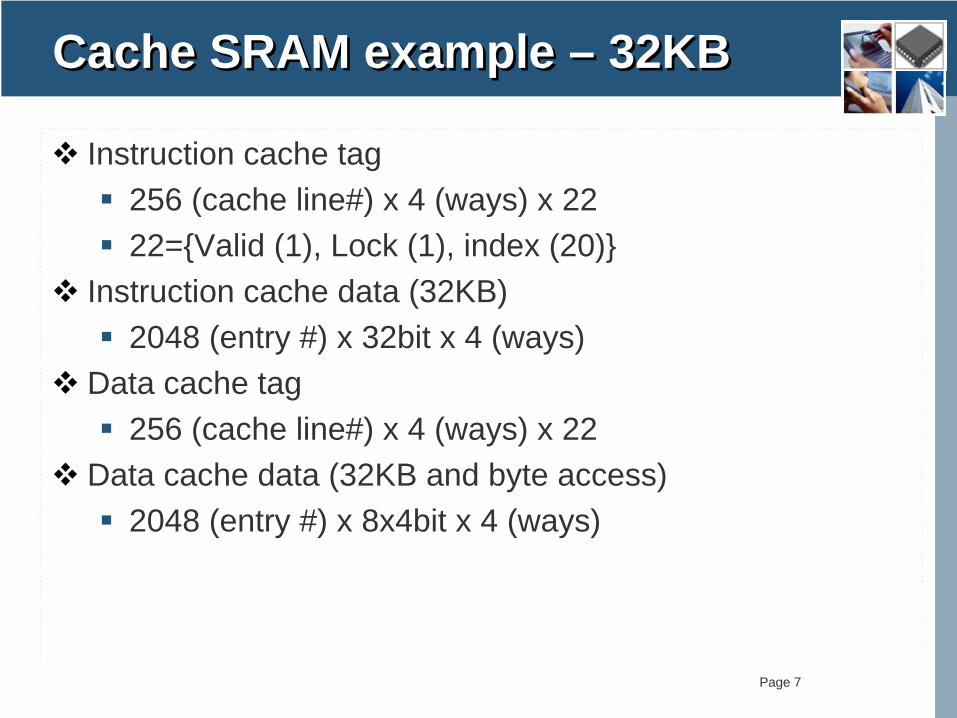
Instruction cache tag256 (cache line#) x 4 (ways) x 22 22={Valid (1), Lock (1), index (20)}
Instruction cache data (32KB)2048 (entry #) x 32bit x 4 (ways)
Data cache tag256 (cache line#) x 4 (ways) x 22
Data cache data (32KB and byte access)2048 (entry #) x 8x4bit x 4 (ways)

Page 8
N1213-S Cache configurationN1213-S Cache configurationCache sets per way
128/256/512Cache ways
2/4 waysCache line size
16B/32BCache size combination
256X16BX2=8KB128X32BX2=8KB256X16BX4=16KB 512X16BX2=16KB128X32BX4=16KB256X32BX2=16KB256X32BX4=32KB 512X32BX2=32KB512X16BX4=32KB1024X16BX2=32KB512X32BX4=64KB1024X16BX4=64KB
Page 9
Cache replacement algorithmCache replacement algorithm
Pseudo LRU (default)Random

Page 10
MTLB entry:63bitMTLB entry:63bitMTLB tag
VPN[31:12]: Virtual page number• 4KB : VPN[31:12]• 8KB : VPN[31:13]
CID[8:0]:process IDG :Global bitS :S=1 1MB page tableValidLock
MTLB data D : dirty bitX : executable bitA : accessed bitPPN[31:12]: Physical page numberC[2:0] : Cacheability attributesM[2:0] :Access privilege for user and superuser mode
MTLB configuration options32x4=12816x4=648x4=32

Page 11
Caching Applied to Address TranslationCaching Applied to Address Translation
Process references the same page repeatedlyTranslating each virtual address to physical address is wasteful
Translation lookaside buffer (TLB)Track frequently used translationsAvoid translations in the common case

Page 12
Caching Applied to Address TranslationCaching Applied to Address Translation
Virtual addresses
Physicaladdresses
Data reads or writes(untranslated)
TLB
Translation table
In TLB
Page 13
Example of the TLB ContentExample of the TLB Content
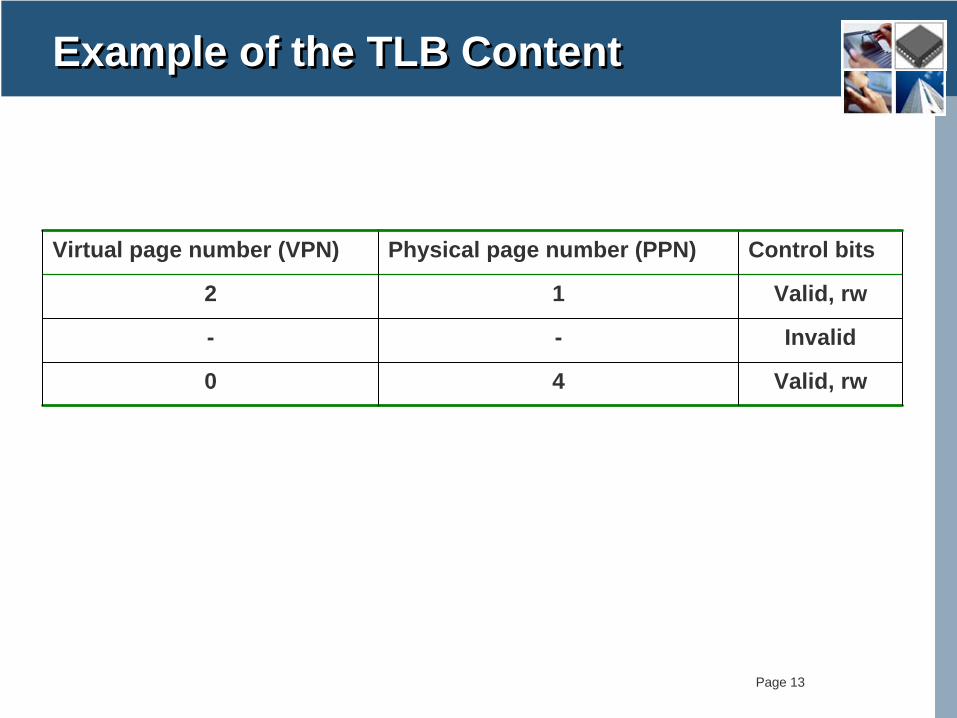
Virtual page number (VPN) Physical page number (PPN) Control bits
2 1 Valid, rw
- - Invalid
0 4 Valid, rw

Page 14
TLB LookupsTLB Lookups
Sequential search of the TLB tableDirect mapping: assigns each virtual page to a specific slot in the TLB
e.g., use upper bits of VPN to index TLB

Page 15
Direct MappingDirect Mapping
if (TLB[UpperBits(vpn)].vpn == vpn) {return TLB[UpperBits(vpn)].ppn;
} else {ppn = PageTable[vpn];TLB[UpperBits(vpn)].control = INVALID;TLB[UpperBits(vpn)].vpn = vpn;TLB[UpperBits(vpn)].ppn = ppn;TLB[UpperBits(vpn)].control = VALID | RWreturn ppn;
}

Page 16
Direct MappingDirect Mapping
When use only high order bitsTwo pages may compete for the same TLB entry
• May loss out needed TLB entriesWhen use only low order bits
TLB reference will be clustered• Failing to use full range of TLB entries
Common approach: combine both

Page 17
TLB LookupsTLB Lookups
Set associatively: use N TLB banks to perform lookups in parallel

Page 18
Two-Way Associative CacheTwo-Way Associative Cache
VPN
VPN PPN
VPN PPN
VPN PPN
VPN PPN
VPN PPN
VPN PPN
hash
= =
If miss, translate and replace one of the entries

Page 19
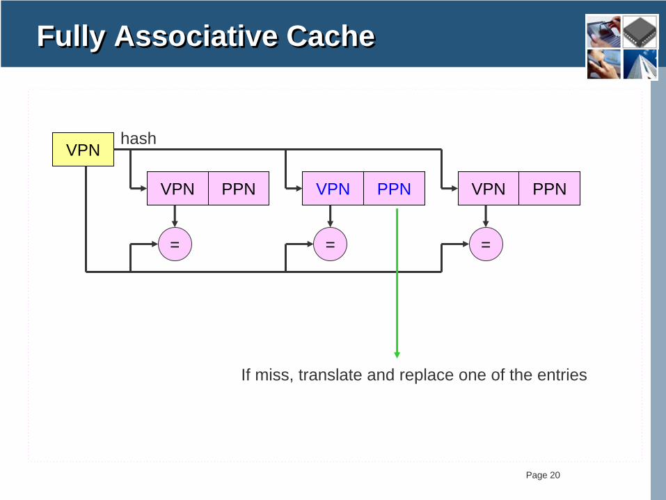
TLB LookupsTLB Lookups
Fully associative cache: allows looking up all TLB entries in parallel
Page 20
Fully Associative CacheFully Associative Cache
VPN
VPN PPN VPN PPN
hash
VPN PPN
= = =
If miss, translate and replace one of the entries

Page 21
TLB LookupsTLB Lookups
TypicallyTLBs are small and fully associativeHardware caches use direct mapped or set-associative cache

Page 22
Replacement of TLB EntriesReplacement of TLB Entries
Direct mappingEntry replaced whenever a VPN mismatches
Associative cachesRandom replacementLRU (least recently used)MRU (most recently used)Depending on reference patterns
Page 23
Replacement of TLB EntriesReplacement of TLB Entries
Hardware-levelTLB replacement is mostly random
• Simple and fastSoftware-level
Memory page replacements are more sophisticatedCPU cycles vs. cache hit rate

Page 24
Consistency Between TLB and Page Tables Consistency Between TLB and Page Tables
Different processes have different page tablesTLB entries need to be invalidated on context switchesAlternatives:
• Tag TLB entries with process IDs• Additional cost of hardware and comparisons per
lookup
Page 25
Relationship Between TLB and HW Memory Caches Relationship Between TLB and HW Memory Caches
We can extend the principle of TLBVirtually addressed cache: between the CPU and the translation tablesPhysically addressed cache: between the translation tables and the main memory

Page 26
Relationship Between TLB and HW Memory Caches Relationship Between TLB and HW Memory Caches
Data reads or writes(untranslated)
VA data
VA data
Virtually addressed cache
TLB PA data
PA data
Physically addressed cache
PA data
PA dataPA data
PA data
Translation tables

Page 27
Support Inter./ext. vector interruptSupport Inter./ext. vector interrupt
Internal vector interruptwhere interrupts are prioritized inside an AndesCore™Hw0 has highest priority
External Vectored Interruptwhere interrupts are prioritized outside AndesCoreusing an external interrupt controller.
The size of the vectored entry point can be from 4 bytes to 16/64/256 bytes.
Page 28
Local memoryLocal memory
Internal or external local memory configuration optionsTwo different access modes for internal local memory
Normal access modeDouble buffer mode
• 2 bank structure• ½ local memory size • CPU and DMA can access the same time

Page 29
DMA DMA
DMA Controller
Local Memory
Ext. Memory
Two channels One active channelOnly accessed by superuser modeFor both instruction and data local
memoryExternal address can be incremented
with strideOptional 2-D Element Transfer from
external memory
N1213-S
1D/2D
Page 30
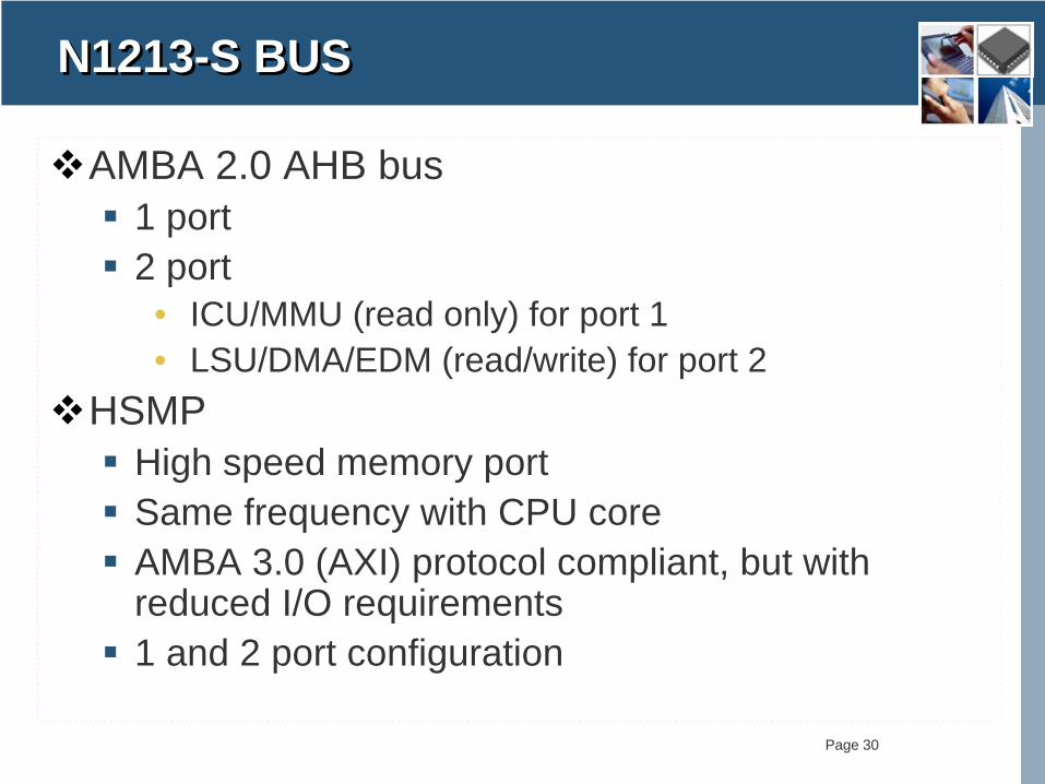
N1213-S BUSN1213-S BUS
AMBA 2.0 AHB bus1 port 2 port
• ICU/MMU (read only) for port 1 • LSU/DMA/EDM (read/write) for port 2
HSMPHigh speed memory portSame frequency with CPU coreAMBA 3.0 (AXI) protocol compliant, but with reduced I/O requirements1 and 2 port configuration

Page 31
N1213-S Debug environment N1213-S Debug environment
CPU core
N1213-S
EDMExternal ICE
AndeSICE
In circuit emulator
USB

Page 32
EDM (Embedded Debug Module) block diagramEDM (Embedded Debug Module) block diagram
N1213-S
TAP:JTAG style interfaceDIMU:Store debug program
BCU: Breakpoint compare unit

Page 33
Performance MonitorPerformance Monitor
CPU Clock Cycle
CPU Instruction Executions …
Memory and Cache Access Cache Miss Event
Instruction Counting
CPU Cycle Counting
Performance Counter 1Performance Counter 2
Performance Counter 0
Branch or Other Events …

Page 34
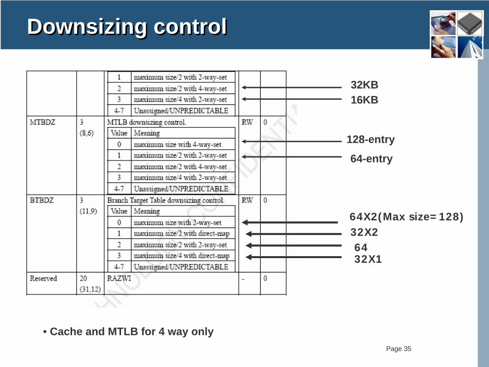
Downsizing controlDownsizing control
Page 35
Downsizing controlDownsizing control
64X2(Max size=128)
6432X2
32X1
32KB16KB
128-entry
64-entry
• Cache and MTLB for 4 way only
Page 36
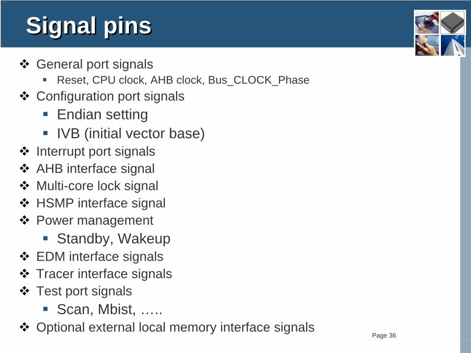
Signal pinsSignal pinsGeneral port signals
Reset, CPU clock, AHB clock, Bus_CLOCK_PhaseConfiguration port signals
Endian settingIVB (initial vector base)
Interrupt port signalsAHB interface signalMulti-core lock signalHSMP interface signalPower management
Standby, WakeupEDM interface signalsTracer interface signalsTest port signals
Scan, Mbist, …..Optional external local memory interface signals

Page 37
Clock ratioClock ratio
The clock bus ratio between CPU core and AMBA bus clock are 1/1,2/1,3/1,4/1,5/1,6/1,3/2,5/2,8/1,10/1,12/1,14/1,15/1,18/1,20/1.
Clock divider is not part of AndesCoreWhile the high speed memory bus clock is the same with CPU core clock.

Page 38
Configuration optionsConfiguration options
Cache size (I & D)256X16BX2=8KB128X32BX2=8KB256X16BX4=16KB512X16BX2=16KB128X32BX4=16KB256X32BX2=16KB256X32BX4=32KB 512X32BX2=32KB512X16BX4=32KB1024X16BX2=32KB512X32BX4=64KB1024X16BX4=64KBDirect map 2 or 4 bankWrite through only (D cache)
Cache policyPseudo-LRU (default), Random
Page 39
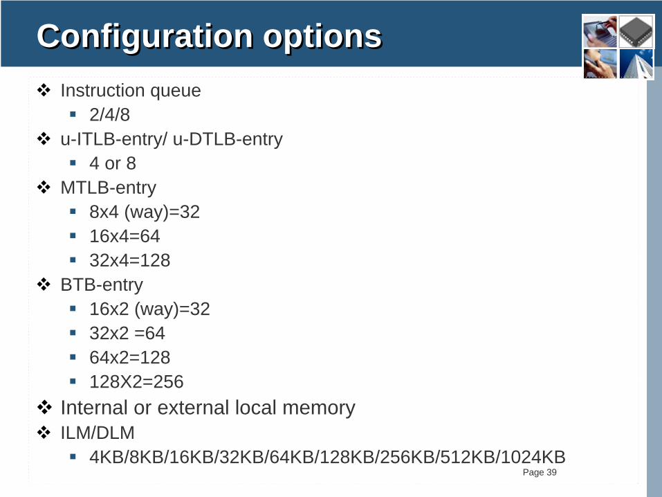
Configuration optionsConfiguration optionsInstruction queue
2/4/8u-ITLB-entry/ u-DTLB-entry
4 or 8MTLB-entry
8x4 (way)=3216x4=6432x4=128
BTB-entry16x2 (way)=3232x2 =6464x2=128128X2=256
Internal or external local memoryILM/DLM
4KB/8KB/16KB/32KB/64KB/128KB/256KB/512KB/1024KB

Page 40
Configuration optionsConfiguration options
AHB port1 or 2
HSMP1 or 2
AHB clock synchronization Synchronous (default) or Asynchronous
EDM break point0/1/2/3/4/5/6/7/8

Page 41
Configuration optionsConfiguration options
Optional (exist or not)HPTW (hardware page table walker)16bit ISAPerformance extension ISAMAC related ISA (refer to MSC_CFG)ICEEPT interfacePerformance monitorGated clock

Page 42
Configuration Options (1)Configuration Options (1)

Page 43
Configuration Options (2)Configuration Options (2)

Page 44
EDA toolsEDA tools
SynthesizerSynopsys Design Compiler
SimulatorCadence Incisive
Formal verificationCadence Formality
STASynopsys PrimeTime
FPGASynplicity +Xilink

Page 45
N1213 on UMC 0.13HS processN1213 on UMC 0.13HS processItems Values
Product name N1213_43U1H (Hardcore)Fab/process UMC/L130E-HSBranch prediction entry number 128I Cache size (Bytes) 32KD Cache size (Bytes) 32KCache line size (Bytes) 32Cache associative (way) 4I Local memory (Bytes) 16KD Local memory (Bytes) 16KiTLB (fully associative) entry number 4dTLB (fully associative) entry number 8Main TLB (4-way set associative) entry number 128 Hardware page table walker yesDMA yesMax Clock Frequency (*Worst case) (Mhz) 500Size (mm2) 3.44x 2.31Number of metal layers used 6
* 1.08V 125C slow silicon
Page 46
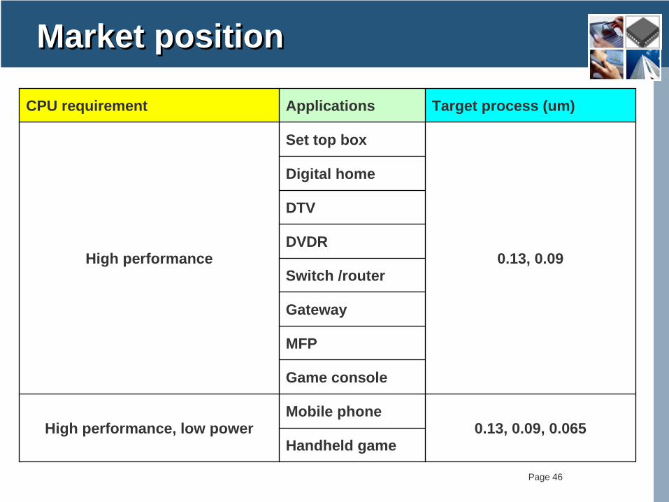
Market positionMarket position
CPU requirement Applications Target process (um)
High performance
Set top box
0.13, 0.09
Digital home
DTV
DVDR
Switch /router
Gateway
MFP
Game console
High performance, low powerMobile phone
0.13, 0.09, 0.065Handheld game

www.andestech.com47
Thank YouThank You