andra´s perl, david n. reinhoudt, and jurriaan huskens- microcontact printing: limitations and...
TRANSCRIPT
8/3/2019 Andra´s Perl, David N. Reinhoudt, and Jurriaan Huskens- Microcontact Printing: Limitations and Achievements
http://slidepdf.com/reader/full/andras-perl-david-n-reinhoudt-and-jurriaan-huskens-microcontact-printing 1/12
Microcontact Printing: Limitations and Achievements
By Andras Perl, David N. Reinhoudt, and Jurriaan Huskens*
1. Introduction
Miniaturization of materials constitutes one of the main researchand development trends in material sciences in the last few decades. Products of micro- and nanotechnology offer severaladvantages over conventional macroscopic functional structures:
lower energy consumption, higher efficiency, and many unexplored but possible benefits arriving from the propertiesof the materials at micro- and nanometer lengthscales. Two mainlines of micro- and nanofabrication strategies have evolved:bottom-up and top-down methods.
Top-down fabrication methods shape structures from bulk material producing new types of small structures based onminiaturization. Lithography is the most successful class of top-down techniques, which include photolithography andnon-photolithographic methods.[1] Nowadays, for the fabricationof microelectronic devices, photolithography is exclusively used.Despite the fact that it is an expensive technique with costly instruments, it has proven to be the most viable method in themicroelectronic market, and no other fabrication method has
been able to compete.Bottom-up methods build highly ordered micro- and nano-
structures from smaller elementary components. The most efficient and applied method is the self-assembly of molecules
or (nano)particles. When self-assembly isapplied to a solid surface, the verticalnanometer dimensions of structures areinstantaneously achieved with the creationof self-assembled monolayers (SAMs).[2–4]
Self-assembly has the potential of creatinghighly ordered and multifunctional micro-and nanostructures,[5] but until the inven-tion of soft lithography, in particularmicrocontact printing (mCP), the possibility of area and volume pattern fabrication by bottom-up methods was very limited. Thecombination of self-assembly of SAMs withthe large-area surface-patterning capabil-ities of top-down techniques, initiated by Whitesides, has opened the way for cheapand easily accessible nanofabrication.[6–9]
Despite its many advantages, mCP did not prove to be a competitive alternative for photolithography in thesemiconductor industry. However, continuous efforts to improvemCP bring forth a spectacular increase in applicability andversatility in other areas.
Here, we will review the emergence of different mCP methodsand strategies that offer possibilities for new applications that render mCP a powerful surface-patterning technique.
2. Microcontact Printing: Principles and theMain Limitations
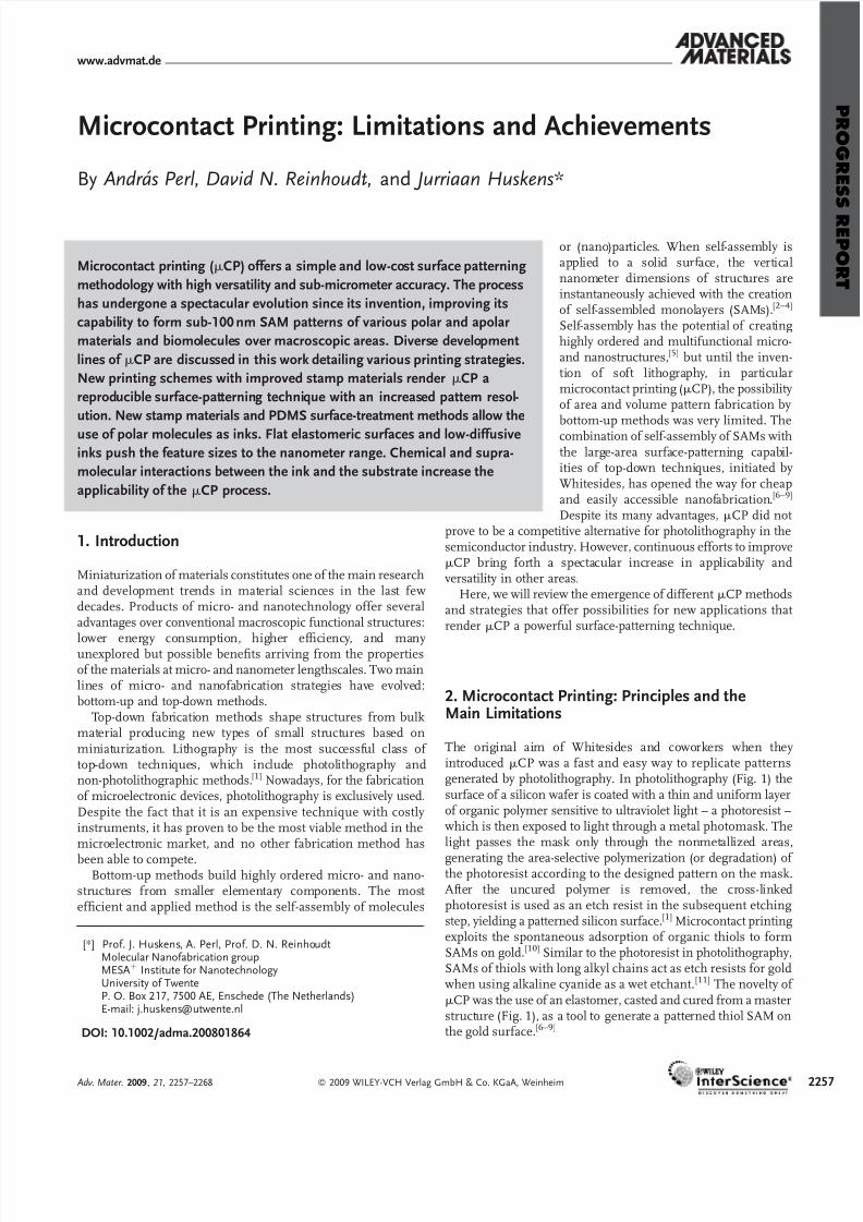
The original aim of Whitesides and coworkers when they introduced mCP was a fast and easy way to replicate patternsgenerated by photolithography. In photolithography (Fig. 1) thesurface of a silicon wafer is coated with a thin and uniform layerof organic polymer sensitive to ultraviolet light – a photoresist –which is then exposed to light through a metal photomask. Thelight passes the mask only through the nonmetallized areas,
generating the area-selective polymerization (or degradation) of the photoresist according to the designed pattern on the mask.After the uncured polymer is removed, the cross-linkedphotoresist is used as an etch resist in the subsequent etchingstep, yielding a patterned silicon surface.[1] Microcontact printingexploits the spontaneous adsorption of organic thiols to formSAMs on gold.[10] Similar to the photoresist in photolithography,SAMs of thiols with long alkyl chains act as etch resists for goldwhen using alkaline cyanide as a wet etchant.[11] The novelty of mCP was the use of an elastomer, casted and cured from a masterstructure (Fig. 1), as a tool to generate a patterned thiol SAM onthe gold surface.[6–9]
www.advmat.de
[*] Prof. J. Huskens, A. Perl, Prof. D. N. ReinhoudtMolecular Nanofabrication groupMESAþ Institute for NanotechnologyUniversity of TwenteP. O. Box 217, 7500 AE, Enschede (The Netherlands)E-mail: [email protected]
DOI: 10.1002/adma.200801864
Microcontact printing (mCP) offers a simple and low-cost surface patterning
methodology with high versatility and sub-micrometer accuracy. The process
has undergone a spectacular evolution since its invention, improving its
capability to form sub-100 nm SAM patterns of various polar and apolar
materials and biomolecules over macroscopic areas. Diverse development
lines of mCP are discussed in this work detailing various printing strategies.
New printing schemes with improved stamp materials render mCP a
reproducible surface-patterning technique with an increased pattern resol-
ution. New stamp materials and PDMS surface-treatment methods allow the
use of polar molecules as inks. Flat elastomeric surfaces and low-diffusiveinks push the feature sizes to the nanometer range. Chemical and supra-
molecular interactions between the ink and the substrate increase the
applicability of the mCP process.
Adv. Mater. 2009, 21, 2257–2268 ß 2009 WILEY-VCH Verlag GmbH & Co. KGaA, Weinheim 2257
8/3/2019 Andra´s Perl, David N. Reinhoudt, and Jurriaan Huskens- Microcontact Printing: Limitations and Achievements
http://slidepdf.com/reader/full/andras-perl-david-n-reinhoudt-and-jurriaan-huskens-microcontact-printing 2/12
www.advmat.de
Microcontact printing uses a hard silicon master or any solidpatterned surface as a template (Fig. 1). A poly(dimethylsiloxane)(PDMS) elastomer is typically used to transfer the pattern fromthe template to the substrate. In most mCP experiments, acommercially available two-component siloxane polymer (Sylgard
184, Dow Corning) is used. In the stamp-preparation step, theliquid vinyl-terminated prepolymer and the curing agent, whichconsists of a short hydrosilane crosslinker containing a platinumcomplex as a catalyst, are mixed and the mixture is poured ontothe patterned template.[12] The PDMS is cured at elevatedtemperatures (usually 60 8C), and a solid but elastomeric polymeris formed. The PDMS product is a crosslinked polymercontaining the –Si(CH3)2–O– structural unit.[13]
After peeling off the PDMS, the stamp is cut to proper size and,in the inking step, saturated with a thiol. The highly hydrophobicPDMS material allows only the use of apolar inks. Wet inking isachieved either by immersion of the stamp in the ink solution or
by placing a few droplets of the thiol solution on the patternedside of the stamp. Hydrophobic long-chain thiols reside not only on the stamp surface but diffuse into the bulk of the stampmaterial, creating an ink reservoir.[14] After inking, the solvent (ethanol) is evaporated in a stream of nitrogen, and the stampsurface is dried. By bringing the inked stamp in conformal
contact with the gold surface, the thiol is transferred to the
Andras Perl studied chemistry atthe Babes-Bolyai University,Romania and the University of Twente, The Netherlands. In2003 he obtained his masterdegree with Prof. Uwe Karst.Since 2004 he is a PhD student inthe Molecular Nanofabricationgroup, University of Twente. Hiswork, supervised by Prof. Jurriaan
Huskens and Prof. David N. Reinhoudt, deals with mono-
layer-assisted assembly, soft lithography and surfacespreading kinetics of multivalent host-guest systems.
David N. Reinhoudt obtained hisPhD with Prof. H. C. Beijerman(Delft University of Technology).He was appointed as a part-timeprofessor in 1975 at the Univer-sity of Twente, and became fullprofessor in 1978. His research isfocused on supramolecularchemistry and technology with
nanofabrication, molecularrecognition, and noncovalent combinatorial synthesis as themajor fields. He is in charge of the Laboratory of Supramolecular Chemistry and Technology, and chairman of the Board of NanoNed, the Dutch program forNanotechnology.
Jurriaan Huskens obtained hisPhD with Prof. Herman vanBekkum and Joop Peters from theDelft University of Technology.After postdoctoral stays withProf. Dean Sherry and Prof.Manfred Reetz, he became anAssistant, and later Associate,Professor in the group of Prof.David Reinhoudt at the Universityof Twente. Since September 2005he has been full professor Mole-
cular Nanofabrication at the same university. Present researchinterests encompass supramolecular chemistry at interfaces,multivalency, supramolecular materials, and nanofabricationmethodologies.
Figure 1. Schematic comparison of photolithography versus mCP. Thecrucial step in both techniques consists of the accurate transfer of thepatterned etch-resist layer.
258 ß 2009 WILEY-VCH Verlag GmbH & Co. KGaA, Weinheim Adv. Mater. 2009, 21, 2257–2268

8/3/2019 Andra´s Perl, David N. Reinhoudt, and Jurriaan Huskens- Microcontact Printing: Limitations and Achievements
http://slidepdf.com/reader/full/andras-perl-david-n-reinhoudt-and-jurriaan-huskens-microcontact-printing 3/12
www.advmat.de
surface.[4,15] Automated printing using a microcontact printer hasbeen recently demonstrated.[16] Due to the patterned structure of the stamp, only the areas with protrusions are able to contact thegold surface, and the thiol is area-selectively transferred accordingto the pattern of the template. If the concentration of the inkingsolution used is higher than a few mM, the order and quality of the
SAMs of long-chain thiols formed by printing are indistinguish-able from those formed in solution.[4,17]
In the wet-etching step, the patterned gold sample is immersedin an etching solution and the unprotected gold is etched away,while the areas covered by long-chain thiol SAMs remain mostly intact. By this selective etching of the sample, the inverse replicaof the surface relief from the original template is created in thegold substrate. Disorder and pinholes in the thiol SAM can alsolead to some etching in the protected areas, but the etch rates of the protected and bare gold areas are usually sufficiently different.Methyl-terminated thiols with long alkyl chains provide a goodprotection from etching. Shorter alkanethiols and polar group-terminated thiols provide a less effective protection.[7] Recently, it was shown that aliphatic dithiocarboxylic acids also form
etch-protective SAMs on gold surfaces.[18]Soon after the initial publications on mCP with alkanethiols on
gold, other metals were successfully used as substrates to achievepattern replication, such as Ag,[19,20] Cu,[21] and Pd.[22] The low costs and simplicity of the technique have inspired the interest increating smaller patterns with higher edge resolution, and inbroadening the versatility of the technique. However, severallimitations have hindered the reproducible creation of sub-micrometer features.
The stamp deformation during stamp removal from thetemplate and during the contacting of the substrate limits theresolution of the patterning.[23–26] The mechanical properties of the elastomeric PDMS stamps provide sufficient mechanical
stability for the printing down to 500 nm.
[13]
The height of thefeatures divided by their lateral dimensions defines the aspect ratio of a pattern.[23] When the aspect ratio is high, buckling andlateral collapse of the PDMS features can occur, while at low aspect ratios roof collapse is possible (Fig. 2A).[25,27] Any deformation of the stamp will affect the printed pattern anddecrease reproducibility.
The PDMS crosslinking process typically leaves some uncuredand low-molecular-weight fragments that may contaminate thesubstrate upon contacting, thus decreasing the quality of the
printed SAM.[28–30] The transfer of these impurities is enhancedwhen the ink molecules contain polar groups.[31]
Almost all organic solvents induce swelling of the PDMSstamp, changing the dimensions and shape of the protrusions.[32]
Ethanol has a minimal swelling effect on the polymer, but many other solvents cannot be used for wet inking of the stamp due to
their pronounced swelling,
[33]
therefore the mCP process islimited to apolar inks that are soluble in ethanol.Due to the hydrophobic surface properties of PDMS, water-
soluble inks do not wet the surface of the elastomer and do not permeate the bulk, restricting the usage of, for example, inorganiccomplexes and biomolecules.[13] The oxidation of the PDMSsurface (by oxygen plasma, for exmaple) allows the printing of such polar inks owing to the polar, thin silica-like surface layerformed upon oxidation.[34] However, this silica-like layer hasdifferent mechanical properties from PDMS, and cracks can beformed on the surface. These cracks allow the migration of low-molecular-weight PDMS fragments leading to the recovery of the hydrophobic character of the surface,[34,35] a process that occurs within a few hours after oxidation and that limits the
applicability and reuse of an oxidized stamp. [36,37]The formation of an ordered SAM on the substrate is typically
achieved by ink diffusion from the PDMS bulk to thesurface.[38,39] Mobility of the inks causes a lateral spreadingfrom the edge of the contact region to the noncontacted areas (Fig.2B, path 1).[40,41] When sub-micrometer features are transferredvia mCP, this surface spreading can significantly influence thepattern as a function of the printing time and the ink concentration in the stamp.[41] Moreover as a function of thevapor pressure, temperature, and humidity, inks can diffusethrough the ambient vapor phase reaching surface areaswhere no ink is desired (Fig. 2B, path 2).[42,43]
In Biebuyck’s and Whitesides’ approximation,[44] monolayers
spread across a surface as a liquid precursor film consisting of unbound molecules. The binding and organization of themolecules to the substrate alters the surface energy of the substrate having an influence on the interaction of thesurface with both the liquid precursor and the ambient. Thealtered surface energy could favor the expansion of the liquidprecursor (reactive spreading) or inhibit the spreading (autop-hobic spreading and autophobic pinning).[44] They suggested that the lateral spreading of inks could be suppressed by a deliberatedesign of systems where the interfacial tension and the kinetics of organization of the SAMs limit the spreading of the precursorliquid. Later, Biebuyck and coworkers stated that the role of autophobic pinning in lateral spreading during mCP is probably irrelevant, as the surface-to-volume ratio of the ink source
generated by the stamp is increased and a large percentage of the applied ink volume is consumed by the formation of theprecursor film.[42] The total quantity of ink available has a morepronounced effect on the spreading of the ink. The concentrationof the ink solution used while inking plays a crucial role in thespreading rate; the surface spreading is faster at higher ink concentrations.[41,42]
With the emergence of dip-pen nanolithography, in which anatomic force microscopy (AFM) tip coated with a molecular ink isused to transfer molecules to a substrate, [45] new studies andmodels that deal with the diffusion of thiols on gold have beendeveloped. Sheehan and Whitman assumed that the lateral
Figure 2. The pattern resolution and reproducibility of the mCP process ismainly limited by stamp deformation (A: buckling, left, and roof collapse,right) and diffusion phenomena of the ink (B) along the surface (1) andthrough the ambient (2).
Adv. Mater. 2009, 21, 2257–2268 ß 2009 WILEY-VCH Verlag GmbH & Co. KGaA, Weinheim 2259
8/3/2019 Andra´s Perl, David N. Reinhoudt, and Jurriaan Huskens- Microcontact Printing: Limitations and Achievements
http://slidepdf.com/reader/full/andras-perl-david-n-reinhoudt-and-jurriaan-huskens-microcontact-printing 4/12
www.advmat.de
spreading of a SAM from an ink source obeys Fick’s laws.[46] Inthis model, the coverage of the surface is decreasing with thedistance from the ink source. The boundary of a SAM detectableby AFM is determined by a critical surface concentration forwhich the standing orientation of the adsorbed thiols is obtained.The model faithfully describes the lateral spreading empirically
found; however, it also implies the dispersion of a densemonolayer pattern, which has not been observed experimentally.Ratner and coworkers introduced a diffusion model wherespreading is possible only over SAM-covered regions.[47] Ink molecules coming from the source are immediately trapped andimmobilized by available adsorption sites at the surface. When allnearby surface sites are occupied, new ink molecules migratefrom the source across the covered region, thus continuously moving the boundary of the SAM-covered area.[47]
To overcome the limitations of the original mCP technique,several alternatives have been developed either by changing theprinting procedure itself or by varying the properties of the ink orthe stamp. New ink materials have been introduced to controlspreading and to enrich the variety of the applicable substrates
and immobilized molecules. Parallel to the appearance of thesenew strategies and methods, the objective has slowly shifted from3D pattern replication toward high-resolution surface patterningof chemical templates in surface-related applications.
3. Alternative mCP Strategies
3.1. High-Speed mCP
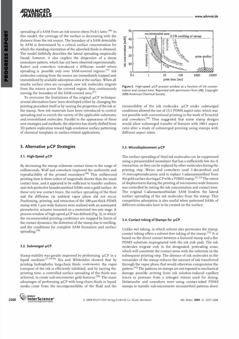
By decreasing the stamp–substrate contact times to the range of milliseconds, Wolf and coworkers improved the uniformity andreproducibility of the printed monolayer.[48] This millisecond
printing time is three orders of magnitude shorter than the usualcontact time, and it appeared to be sufficient to transfer uniformand etch-protective hexadecanethiol SAMs onto a gold surface. At these very low contact times, the surface spreading of the thioland the diffusion via ambient vapor phase did not occur.Positioning, printing, and retraction of the 100-mm-thick PDMSstamp with 1-mm-wide features were realized with an automatedpiezoelectric actuator mounted on a motorized two-axis stage. Aprocess window of high-speed mCP was defined (Fig. 3), in whichthe recommended printing conditions are mapped by limits of the contact dynamics, the distortion of the stamp due to swelling,and the conditions for complete SAM formation and surfacespreading.[48]
3.2. Submerged mCP
Stamp stability was greatly improved by performing mCP in aliquid medium.[27,49,50] Xia and Whitesides showed that by printing hydrophobic long-chain thiols underwater, the vaportransport of the ink is efficiently inhibited, and by varying theprinting time, a controlled surface spreading of the thiols wasachieved, to create sub-micrometer gold features. [50] The mainadvantages of performing mCP with long-chain thiols in liquidmedia come from the incompressibility of the fluid and the
immiscibility of the ink molecules. mCP under submergedconditions allowed the use of 15:1 PDMS aspect ratio, which wasnot possible with conventional printing in the work of Errachid
and coworkers.[49] They suggested that some stamp designswould allow submerged transfer of features with 100:1 aspect ratio after a study of submerged printing using stamps withdifferent aspect ratios.
3.3. Microdisplacement mCP
The surface spreading of thiol ink molecules can be suppressedusing a preassembled monolayer that has a sufficiently low Au–Sinteraction, so they can be replaced by other molecules during theprinting step. Weiss and coworkers used 1-decanethiol and11-mercaptoundecanoic acid to replace 1-adamantanethiol from
the gold surface duringmCP with a PDMS stamp.[51,52] The extent of displacement during the printing of micrometer-wide featureswas controlled by tuning the ink concentration and contact time.The original 1-adamantanethiolate SAM hinders the lateralsurface spreading of the ink molecules from the stamp. Thiscompetitive adsorption is also useful when patterned SAMs of different molecules have to be created on the surface.
3.4. Contact Inking of Stamps for mCP
Unlike wet inking, in which solvent also permeates the stamp,contact inking offers a solvent-free inking of the stamp. [53] It is
based on the direct contact between a featured stamp and a flat PDMS substrate impregnated with the ink (ink pad). The ink molecules migrate only to the designated, protruding areas,which will constitute the contact areas with the substrate in thesubsequent printing step. The absence of ink molecules in theremainder of the stamp reduces the amount of ink transferredthrough the vapor phase that would otherwise compromise thepattern.[42] The patterns on stamps are not exposed to mechanicaldamage possibly arriving from ink solution-induced capillary forces or pressure from a nitrogen stream used for drying.Delamarche and coworkers were using contact-inked PDMSstamps to transfer sub-micrometer eicosanethiol patterns down
Figure 3. High-speed mCP process window as a function of ink concen-tration and contact time. Reprinted with permission from [48]. Copyright2006 American Chemical Society.
260 ß 2009 WILEY-VCH Verlag GmbH & Co. KGaA, Weinheim Adv. Mater. 2009, 21, 2257–2268

8/3/2019 Andra´s Perl, David N. Reinhoudt, and Jurriaan Huskens- Microcontact Printing: Limitations and Achievements
http://slidepdf.com/reader/full/andras-perl-david-n-reinhoudt-and-jurriaan-huskens-microcontact-printing 5/12
www.advmat.de
to 100 nm feature sizes.[53] Both the concentration of the thiolsolution used for the impregnation of the inkpad and the contact time in the printing step affected the surface spreading of thethiol and influenced the etch-protective quality of the printedSAM. These counteracting process factors needed to be balancedwhen minimizing both the surface spreading and the occurrence
of defects in the transferred SAM.
[53]
3.5. Positive mCP
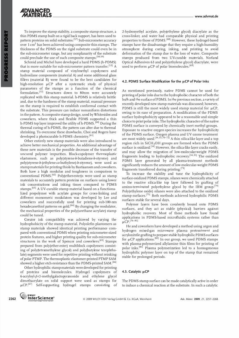
The term ‘positive’ in positive mCP[54] ((þ)mCP) refers to therelation between the master and the obtained replica afteretching. While in the original mCP a given master design leads toa ‘negative’, that is, inverse replica, the (þ)mCP process generatesan identical ‘positive’ replica of the original master, which isachieved using two different inks in the process (Fig. 4). [54] Whilethe first ink used for printing in (þ)mCPdoes not form an orderedetch-protective SAM, a second ink is used to backfill the available
gold surface from solution, thus forming a patterned etch-resistant SAM. Pentaerythritol-tetrakis(3-mercaptopropionate) (PTMP) wasused by Delamarche and coworkers as a positive ink, because it forms a stable SAM on gold and copper, is not replaced by etch-resistant alkanethiols, and does not provide significant etchresistance.[54] High-resolution structures formed on Cu sub-strates indicated that the diffusion characteristics of PTMP aresufficiently low to create patterns at 200 nm length scales. (þ)mCPallows the use of stamps with high fill factors to create inverse,low-fill-factor patterns, overcoming the main stamp-stability problems when creating such features by common (–)mCP.
3.6. Edge-Transfer Lithography
Edge-transfer lithography uses a patterned elastomeric stampinked with an ink solution prepared from solvents that dewet thepatterned surface of the stamp.[55,56] A discontinuous dewettingconfines the ink only to the recessed areas of the stamp. Afterevaporation of the solvent, the inks are selectively transferredfrom the edges of the recessed areas in the printing step, leadingto ink adsorption on the substrate only along the edges of thecontacted areas. Silanes, nanoparticles, and thiols have beensuccessfully transferred with 100-nm-scale resolution usingstamps with micrometer-sized features.[55,56]
4. Modifications of the Stamp
4.1. New Stamp Materials and Composite Stamps
For an accurate and uniform transfer of the ink to the substrate by a stamp, in general two conflicting stamp characteristics areneeded: high mechanical stability of the micro- and nano-structures and good capability to form conformal contact down tothe nanometer scale despite potential substrate roughness. Ahigh mechanical stability requires a high Young’s modulus, while
efficient conformal contact is facilitated by increased elasticity.The physical properties of PDMS are determined by the chemicalformulation of the stamp, the number of monomer units betweenjunctions, the functionalities of the junctions, and by the curingconditions.[13]
Figure 4. Schematic comparison of mCP and (þ)mCP techniques.
Adv. Mater. 2009, 21, 2257–2268 ß 2009 WILEY-VCH Verlag GmbH & Co. KGaA, Weinheim 2261
8/3/2019 Andra´s Perl, David N. Reinhoudt, and Jurriaan Huskens- Microcontact Printing: Limitations and Achievements
http://slidepdf.com/reader/full/andras-perl-david-n-reinhoudt-and-jurriaan-huskens-microcontact-printing 6/12
www.advmat.de
To improve the stamp stability, a composite stamp structure, athin PDMS stamp built on a rigid back support, has been used topattern proteins on solid substrates.[57] Sub-micrometer accuracy over 1 cm2 has been achieved using composite thin stamps. Thethickness of the PDMS on the rigid substrate could even be inthe sub-micrometer range, but any nonplanarity of the substrate
could preclude the use of such composite stamps.
[58,59]
Schmid and Michel have developed a hard PDMS (h-PDMS)that is more suitable for sub-micrometer pattern transfer.[12] Astamp material composed of vinylmethyl copolymers andhydrosilane components (material A) and some additional glassfillers (material B) were found to be the best candidates forhigh-resolution mCP after a systematic study of physicalparameters of the stamps as a function of the chemicalformulation.[12] Structures down to 80nm were accurately replicated with this stamp material. h-PDMS is relatively brittleand, due to the hardness of the stamp material, manual pressureon the stamp is required to establish conformal contact withthe substrate. This pressure can induce nonuniform distortionsin the pattern. A composite stamp design, used by Whitesides and
coworkers, where thick and flexible PDMS supported a thinh-PDMS top layer improved the utility of h-PDMS. [60] During thethermal curing of h-PDMS, the pattern can alter due to thermalshrinking. To overcome these drawbacks, Choi and Rogers havedeveloped a photocurable h-PDMS chemistry.[61]
Other entirely new stamp materials were also introduced toachieve better mechanical properties. An additional advantage of these new materials is the possible decrease of the transfer of uncured polymer impurities. Block-copolymer thermoplasticelastomers, such as poly(styrene-b-butadiene-b-styrene) andpoly(styrene-b-(ethylene-co-buthylene)-b-styrene), were used asstamp materials for printing thiols by Bastiaansen and coworkers.Both have a high modulus and toughness in comparison to
conventional PDMS.
[62]
Poly(ether-ester)s were used as stampmaterials to accurately pattern proteins on surfaces using lowerink concentrations and inking times compared to PDMSstamps.[63] A UV-curable stamp material based on a functiona-lized prepolymer with acrylate groups for cross-linking anddifferent monomeric modulators was developed by Lee andcoworkers and successfully used for printing sub-100-nmhexadecanethiol patterns on gold.[64] By changing the modulator,the mechanical properties of the poly(urethane acrylate) stampcould be tuned.
Greater ink compatibility was achieved by varying thehydrophobicity of the stamp material. Polyolefin plastomers asstamp materials showed identical printing performance com-pared with conventional PDMS when printing micrometer-sized
protein features, and higher printing quality for sub-micrometerstructures in the work of Spencer and coworkers.[65] Stampsprepared from poly(ether-ester) multiblock copolymers consist-ing of poly(tetramethylene glycol) and poly(butylene terephtha-late) segments were used for repetitive printing without reinkingof polar PTMP. The thermoplastic elastomer-printed PTMP SAMshowed a higher etch-resistance than the PDMS-printed SAM. [66]
Other hydrophilic stamp materials were developed for printingof proteins and biomolecules. Hydrogel copolymers of 6-acryloyl-b-O-methylgalactopyranoside and ethylene glycoldimethacrylate on solid support were used as stamps formCP.[67] Self-supporting hydrogel stamps consisting of
2-hydroxyethyl acrylate, poly(ethylene glycol) diacrylate as thecross-linker, and water had comparable physical and printingproperties to those of PDMS.[68] However, these hydrogel-basedstamps have the disadvantage that they require a high-humidity atmosphere during curing, inking, and printing to avoiddeformation of the stamp due to the loss of water. Composite
stamps produced from two UV-curable materials, NorlandOptical Adhesives 63 and poly(ethylene glycol) diacrylate, wereused to perform mCP of polar biomolecules.[69]
4.2. PDMS Surface Modification for the mCP of Polar Inks
As mentioned previously, native PDMS cannot be used forprinting of polar inks due to the hydrophobic character of both thebulk and the surface of PDMS. In the previous section, a variety of recently developed new stamp materials was discussed; however,PDMS is still the most widely used stamp material for mCP,owing to its ease of preparation. A modification of the PDMS
surface hydrophobicity appeared to be a reasonable and simplechoice to print polar inks. The hydrophobic character of the nativePDMS surface is conveyed by chemically inert methyl groups.Exposure to reactive oxygen species increases the hydrophilicity of the PDMS surface. Oxygen plasma and UV ozone treatment are most widely used.[34,35,70–72] A thin silica-like layer and a topregion rich in SiCH2OH groups are formed when the PDMSsurface is oxidized.[34] However, the silica-like layer cracks easily,and may allow the migration of low-molecular-weight PDMSfragments leading to hydrophobic recovery.[34,35] The oxidizedPDMS layer generated by all plasma-treatment methodssignificantly reduces the amount of low-molecular-weight PDMSfragments transferred during printing.[73]
To increase the stability and tune the hydrophilicity of
surface-oxidized PDMS stamps, silanes were chemically attachedto the reactive silica-like top layer followed by grafting of amino-terminated polyethylene glycol by the IBM group.[74]
Poly(ethylene oxide) silanes were also attached to the oxidizedstamp surfaces.[75] Both methods achieved hydrophilic PDMSsurfaces stable for several days.
Polymer layers have been covalently bound onto PDMSsurfaces, and they act as stable (physical) barriers against hydrophobic recovery. Most of these methods have foundapplications in PDMS-based microfluidic systems rather thanmCP.[76–81]
He and coworkers have developed a method using argon andhydrogen mixed-gas microwave plasma pretreatment and
acrylonitrile grafting to prepare stable hydrophilic PDMS surfacesfor mCP applications.[82] In our group, we used PDMS stampswith plasma-polymerized allylamine thin films for printing of polar inks.[83] Plasma polymerization led to a homogeneoushydrophilic polymer layer on top of the stamp that remainedstable for prolonged periods.
4.3. Catalytic mCP
The PDMS stamp surface can be made catalytically active in orderto induce a chemical reaction at the substrate. In such a catalytic
262 ß 2009 WILEY-VCH Verlag GmbH & Co. KGaA, Weinheim Adv. Mater. 2009, 21, 2257–2268
8/3/2019 Andra´s Perl, David N. Reinhoudt, and Jurriaan Huskens- Microcontact Printing: Limitations and Achievements
http://slidepdf.com/reader/full/andras-perl-david-n-reinhoudt-and-jurriaan-huskens-microcontact-printing 7/12
www.advmat.de
mCP scheme, no ink is needed, and therefore the lateralresolution-reducing effect of surface spreading is efficiently sidestepped. In our group, oxidized PDMS stamps wereused to create patterns via covalent modification of preformedSAMs of bis(v-trimethylsiloxyundecyl)disulfide or bis(v-tert -butyldimethylsiloxy-undecyl)disulfide on gold.[84] Triallylsilyl
ethers were easily hydrolyzed to free alcohols in the presenceof an acid. The silicon oxide of oxidized PDMS stamps wassufficiently acidic to induce catalysis in the contacted areas.
Toone and coworkers used piperidine-functionalized polyur-ethane acrylate stamps to promote the catalytic cleavage of the 9-fluorenylmethoxycarbonyl amino-protecting group.[85]
Sub-micrometer patterns were created with this inklessmethod by selective deprotection of (9H -fluoren-9-yl)methyl-11-mercaptoundecylcarbamate SAMs on gold. They extended theuse of catalytic mCP to biochemical substrates by immobilizingexonuclease enzymes on biocompatible poly(acrylamide)stamps and created patterned DNA both on glass and goldsurfaces.[86]
4.4. Printing with Flat Stamps
Patterned SAM formation with flat, featureless stamps in mCPoffers an effective solution to avoid the typical mechanical stampdeformation and ink transport issues in the originalmCP process.When the stamp is flat, no buckling or side and roof collapse canoccur, and the undesired vapor transfer of the ink can beeliminated as well. However, the main difficulty is the area-selective inking or creation of chemical barriers on the stamp’ssurface.
Flat stamps were inked in an area-selective manner using a
robotic spotting system, and then used to fabricate a multiprobearray of amino-modified oligonucleotide spots.[87] The maindisadvantage of this system is the pattern-size limitation that isgiven by the resolution of the spotting system.
Sub-100-nm resolution in protein patterning was achieved inthe work of Delamarche and coworkers by exploiting thedifferences in adhesion of proteins to PDMS and silicon.[88] Aflat PDMS stamp with a homogeneous protein layer was placedon a patterned silicon nanotemplate. With the removal of thestamp due to the less hydrophobic character of silicon comparedto PDMS, proteins were removed (‘‘subtracted’’) from the stampleaving a patterned protein layer on the noncontacted areas. Theseprotein patterns could be subsequently transferred onto anothersubstrate.[88]
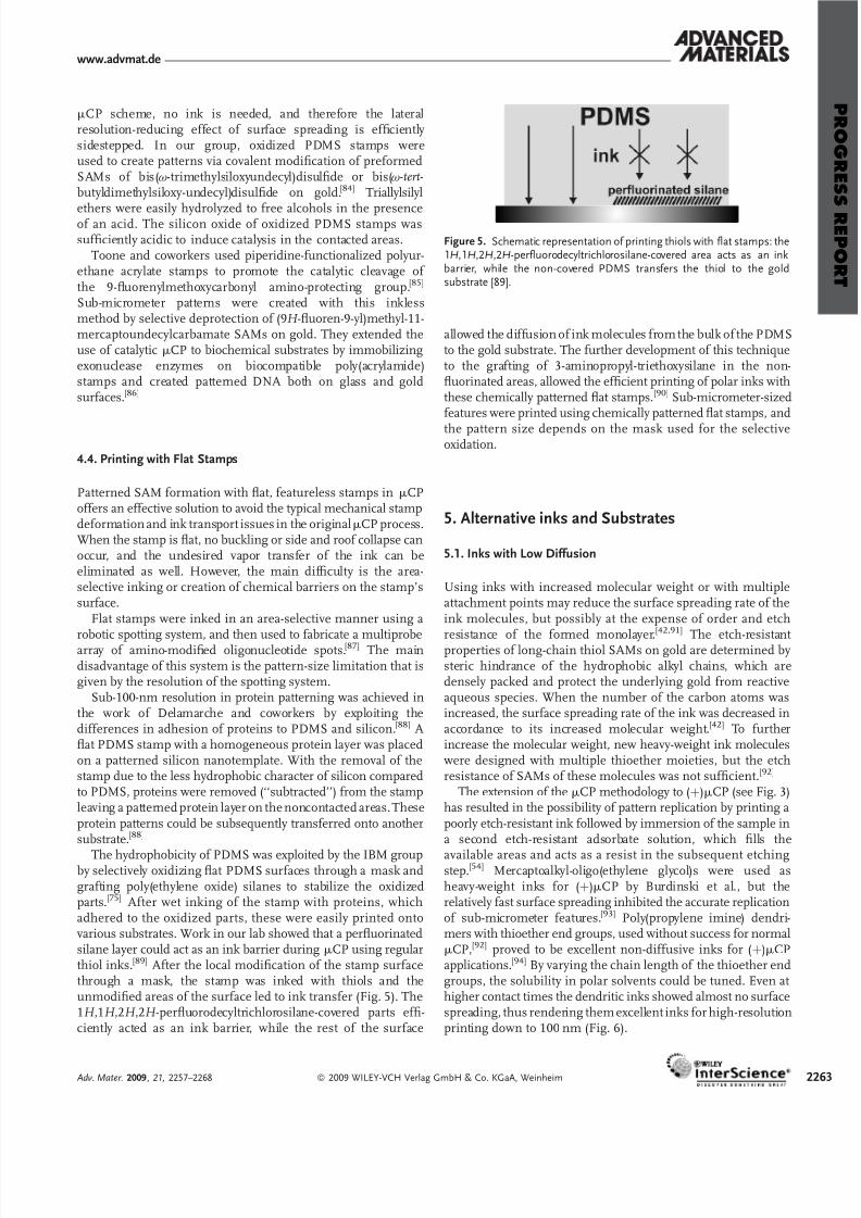
The hydrophobicity of PDMS was exploited by the IBM groupby selectively oxidizing flat PDMS surfaces through a mask andgrafting poly(ethylene oxide) silanes to stabilize the oxidizedparts.[75] After wet inking of the stamp with proteins, whichadhered to the oxidized parts, these were easily printed ontovarious substrates. Work in our lab showed that a perfluorinatedsilane layer could act as an ink barrier during mCP using regularthiol inks.[89] After the local modification of the stamp surfacethrough a mask, the stamp was inked with thiols and theunmodified areas of the surface led to ink transfer (Fig. 5). The1H ,1H ,2H ,2H -perfluorodecyltrichlorosilane-covered parts effi-ciently acted as an ink barrier, while the rest of the surface
allowed the diffusion of ink molecules from the bulk of the PDMSto the gold substrate. The further development of this techniqueto the grafting of 3-aminopropyl-triethoxysilane in the non-fluorinated areas, allowed the efficient printing of polar inks withthese chemically patterned flat stamps.[90] Sub-micrometer-sizedfeatures were printed using chemically patterned flat stamps, and
the pattern size depends on the mask used for the selectiveoxidation.
5. Alternative inks and Substrates
5.1. Inks with Low Diffusion
Using inks with increased molecular weight or with multipleattachment points may reduce the surface spreading rate of theink molecules, but possibly at the expense of order and etch
resistance of the formed monolayer.
[42,91]
The etch-resistant properties of long-chain thiol SAMs on gold are determined by steric hindrance of the hydrophobic alkyl chains, which aredensely packed and protect the underlying gold from reactiveaqueous species. When the number of the carbon atoms wasincreased, the surface spreading rate of the ink was decreased inaccordance to its increased molecular weight.[42] To furtherincrease the molecular weight, new heavy-weight ink moleculeswere designed with multiple thioether moieties, but the etchresistance of SAMs of these molecules was not sufficient. [92]
The extension of the mCP methodology to (þ)mCP (see Fig. 3)has resulted in the possibility of pattern replication by printing apoorly etch-resistant ink followed by immersion of the sample ina second etch-resistant adsorbate solution, which fills the
available areas and acts as a resist in the subsequent etchingstep.[54] Mercaptoalkyl-oligo(ethylene glycol)s were used asheavy-weight inks for (þ)mCP by Burdinski et al., but therelatively fast surface spreading inhibited the accurate replicationof sub-micrometer features.[93] Poly(propylene imine) dendri-mers with thioether end groups, used without success for normalmCP,[92] proved to be excellent non-diffusive inks for (þ)mCPapplications.[94] By varying the chain length of the thioether endgroups, the solubility in polar solvents could be tuned. Even at higher contact times the dendritic inks showed almost no surfacespreading, thus rendering them excellent inks for high-resolutionprinting down to 100 nm (Fig. 6).
Figure 5. Schematic representation of printing thiols with flat stamps: the1H,1H,2H,2H-perfluorodecyltrichlorosilane-covered area acts as an inkbarrier, while the non-covered PDMS transfers the thiol to the goldsubstrate [89].
Adv. Mater. 2009, 21, 2257–2268 ß 2009 WILEY-VCH Verlag GmbH & Co. KGaA, Weinheim 2263

8/3/2019 Andra´s Perl, David N. Reinhoudt, and Jurriaan Huskens- Microcontact Printing: Limitations and Achievements
http://slidepdf.com/reader/full/andras-perl-david-n-reinhoudt-and-jurriaan-huskens-microcontact-printing 8/12
www.advmat.de
5.2. Reactive mCP
In addition to patterning SAMs of sulfur compounds on gold,other adsorbate/substrate systems have been used for mCP inwhich patterning is realized through covalent bonding. Soon afterthe development of conventional mCP, alkylsilanes weresuccessfully printed on silicon oxide.[95–97] Monolayers of silaneson silicon oxide are less well defined than SAMs of thiols on gold,
because the process involves covalent-bond formation, and thuserror correction is limited.[13,98] Lateral spreading limited thepattern resolution in the work of Nuzzo and coworkers when they printed octadecyltrichlorosilane onto silicon.[97,99]
An alternative for the direct patterned SAM formation of complex molecules is offered by the formation of a reactive SAMon a substrate, followed by mCP to locally transfer reagents to thereactive SAM leading to a chemical reaction.[100] Using thismethod, amines and poly(ethylene imines) were printed ontoreactive anhydride or activated carboxylic acid-terminated SAMson gold and silver.[72,101,102] This method was also successfully used by Huck et al. for reacting N-protected amino acids to
surface-confined amino groups when a plasma-oxidized flat PDMS stamp inked with an N -Boc-L-amino acid was put intocontact with an amino SAM.[103] Well-defined functional micro-and nanostructured biointerfaces were fabricated by reactiveprinting of trifluoroacetic acid onto reactive block-copolymerfilms by Schonherr et al.[104,105] The trifluoroacetic acid deprotects
thetert
-butyl acrylate side chains present in the skin layer of theblock-copolymer films, rendering the films chemically reactivewith any amino-terminating (bio)molecule. In another study of the same group, amino end-functionalized poly(ethylene glycol)was printed onto spin-coated thin films of reactive poly (N-hydroxysuccinimidyl methacrylate) to serve as a blockinglayer and prevent nonspecific adsorption of other molecules.[106]
In the work of Downard and coworkers, various diazonium saltswere reacted with pyrolized photoresist films by the use of mCP,creating amino or carboxyl-terminated surface patterns.[107]
Our group has demonstrated the reversible formation of imines through reactive printing of octadecylamine ontoaldehyde-terminated SAMs.[108] The imine pattern obtainedwas stable in water and was completely removed after
acid-catalyzed hydrolysis. We also printed acetylenes ontoazido-terminated SAMs (Fig. 7) by ‘‘click’’ chemistry in thecontact area between the PDMS stamp and the reactive substratewithout the need for a catalyst. [109]
The etching process of the substrate was sidestepped in thelocalized etching method with high-gel-strength agarose, aspresented by Grzybowski and coworkers.[110,111] Localizedetching of silicon and glass substrates was achieved based ondiffusive transport of chemicals within the agarose stamp. Thesubstrate to be structured was placed on top of the inverted andhydrofluoric acid-inked stamp, and the etching in the contact areas took place owing to the diffusive transport of the HF etchant and the reaction product within the stamp.[110]
5.3. Supramolecular mCP
Supramolecular interactions play a pivotal role in biology and arebeing extensively used for other nonbiological applications aswell. The reversible nature of the supramolecular binding of complementary host/guest partners offers flexibility, controllablebinding strength, and dynamics for the controlled positioning of molecules, assemblies, and particles on a substrate. [112]
The combination of mCP with supramolecular host–guest interactions led to various improvements in nanopatterning of (bio)molecules. Proteins were selectively picked up from crude
biological solutions and then printed on substrates by Dela-marche et al.[113] Stamps functionalized with reactive groupsbound the proteins from complex mixtures and aided the transferof these biomolecules onto the chosen substrates. Other groupsimmobilized single-strand DNA on a stamp and immersed it in asolution containing the complementary DNA previously end-functionalized with chemical motifs able to interact with thetargeted substrate. During printing, the preformed ds-DNA isdissociated, and after the removal of the stamp the complemen-tary copy of the master pattern is created. [114–118]
For some years, our group has been exploiting supramolecularinteractions focusing mainly on multivalency on surfaces.
Figure 6. Top: SEM image of gold lines 100nm wide produced by (þ)mCPusing heavy-weight dendritic thioethers as inks and octadecanethiol asbackfilling agent. Bottom: Plot of the width of the ODT-protected stripeareas after (þ)mCP of micrometer-wide features with a dendritic thioetherand PTMP versus the printing time. The concentration (in weight) of theinks was the same in both cases: 0.6 g LÀ1.
264 ß 2009 WILEY-VCH Verlag GmbH & Co. KGaA, Weinheim Adv. Mater. 2009, 21, 2257–2268

8/3/2019 Andra´s Perl, David N. Reinhoudt, and Jurriaan Huskens- Microcontact Printing: Limitations and Achievements
http://slidepdf.com/reader/full/andras-perl-david-n-reinhoudt-and-jurriaan-huskens-microcontact-printing 9/12
www.advmat.de
Molecular printboards, which are self-assembled monolayersfunctionalized with receptor groups, were used as substrates toprint various organic monovalent and multivalent molecules, in
order to study the kinetic and thermodynamic characteristics of these surface-confined complex systems.[112] Suitable guest-functionalized dendrimers, fluorescently labeled molecules,and polymers were used as inks for supramolecular mCP.[119–123]
5.4. Other Inks for mCP
Since the discovery of mCP, various ink materials have beensuccessfully used to pattern surfaces. Advances in printing of biomolecules on various substrates and in general microcontact
processing for biology display the creation of high-performance,miniaturized bioanalytical systems.[124–126]
PDMS contamination was used intentionally to patternsurfaces, and its effect on the assembly of biomolecules wasinvestigated by Inganas and coworkers.[127–129] The resultinghydrophobic patterns were used to direct the stretching of DNA to
specific parts of a surface.
[130]
Poly(methylmethacrylate) (PMMA)-coated PDMS stamps were used to assemble stretched DNAon the stamp surface and transfer it onto the target surface.[130]
A new process, called one-step multiple mCP, developed by Vieu and coworkers, employs a multilevel PDMS stamp that allows the patterning of two different molecules in one step.[131]
The method, based on the elastomeric properties of the PDMSstamp, creates self-aligned patterns of two different molecules by pressuring homogenously the top side of the stamp. The stamplevels inked by two different molecules contact the surfacesequentially. Simultaneous printing of two proteins, bovin serumalbumin (BSA) and streptavidin, was demonstrated. BSA wasprinted on glass by the same group in order to create patterned
self-assembled lipid membranes on surfaces.[132] The BSApattern locally inhibited assembly, while the hydrophilicSiO2 promoted the fusion of liposomes during the incubationstep.
Thin metal layers evaporated on the stamp surface could betransferred onto substrates.[133,134] The process, described by Rogers and coworkers, is called nanotransfer printing (nTP), anduses an adhesive SAM on the substrate to stick to the metal layerand to promote the release of the layer from the stamp when it isremoved. The technique can generate complex patterns without the risk of surface diffusion and edge disorder.
Li and Guo have described the patterning of a conductingpolymer, poly(3,4-ethylenedioxythiophene)/poly(4-styrenesulfonate),
by m
CP on surfaces to create thin-film transistors.
[135]
Colloidal particles and nanoparticles have been printed onvarious substrates.[55,75,136–138] However, the stochastic printingof nanoparticles typically results in patterned, but randomly ordered, particle arrangements. The combined printing andself-assembly of nanoparticles into larger structures was realizedby prearrangement of the particles on the stamp surface prior toprinting. Andres and Santhanam created a uniform nanoparticlelayer on the water/air interface and then transferred theself-assembled particle layer onto a patterned PDMS stamp by bringing the stamp parallel to the water surface and touching thenanoparticle film.[139] Patterned and ordered particle arrays on thesubstrate were formed in the subsequent printing step. Gigli andcoworkers used drop-casting of colloidal semiconductor quantum
dots on glass with controlled evaporation of the solvent, whichallowed the self-assembly of the nanocrystals into large-areaperiodic structures.[140] Conformal contact of a PDMS stamp withthe nanocrystal film was sufficient to ink the stamp and transferthe ordered quantum-dot layer onto small-molecule organiclayers. Wolf and coworkers moved the meniscus of a colloidalsuspension over a patterned layer to self-assemble particles withhigh precision inside the features.[141] The assembly was thenprinted onto the substrate with single-particle resolution.Lines, arrays, and bitmap particle arrangements were createdpreserving the catalytic and optical properties of the individualnanoparticles.[141]
Figure 7. Schematic representation of ‘‘click’’ chemistry by reactive mCP:1-octadecyneis printed ontoan azido-terminatedSAM forming a patternedtriazole layer on the surface [109].
Adv. Mater. 2009, 21, 2257–2268 ß 2009 WILEY-VCH Verlag GmbH & Co. KGaA, Weinheim 2265
8/3/2019 Andra´s Perl, David N. Reinhoudt, and Jurriaan Huskens- Microcontact Printing: Limitations and Achievements
http://slidepdf.com/reader/full/andras-perl-david-n-reinhoudt-and-jurriaan-huskens-microcontact-printing 10/12
www.advmat.de
6. Outlook
Since Whitesides and coworkers developed the mCP technique, aspectacular evolution has followed. While the main concept of thetechnique remained the same (a pattern is transferred onto asurface via conformal contact between an elastomeric stamp andthe substrate), the manner of effectuation and the material of the
constituents showed a diverse development. The mechanicalproperties of the elastomeric stamp material were improved by developing new stamp materials and composite stamp designs.Some stamp materials allowed the use of polar inks, increasingthe applicability of the technique. Parallel to this, new printingconcepts were introduced to use inverse stamp pattern designs oreven flat stamps, the mechanical properties of which becameirrelevant for resolution. Despite a wider variety of new stampmaterials, PDMS remained the cheapest and easiest stampmaterial, causing the popularity of surface-treating techniques tochange the hydrophobicity of the PDMS stamp. Nondiffusiveinks were developed making the sub-100 nm pattern resolutionattainable, while catalytic printing techniques eliminated the
limitations arriving from diffusion.Parallel to the evolution of mCP, the huge potential of the
technique in creating chemical, supramolecular, and biomole-cular patterns on surfaces started to be appreciated. Often themain development efforts were motivated by possible applica-tions in sensing, (bio)analysis, functional nanofabrication, and inbasic research. Using the possibility of creating chemically distinct patterned SAMs, the elemental basics of chemical,supramolecular, and biological interactions could be studied andunderstood. Today, a wide variety of strategies is available to createsurface patterns of both polar and apolar (bio)molecules andnanoparticles on a microscopic scale, while the reproducibleresolution is approaching the sub-100nm range. Mechanicalissues of the stamp were addressed in various ways, and the loss
in pattern resolution due to ink spreading was analyzed andreversed. Despite its original fundamental limits,mCP has provento be a reliable and useful surface-patterning technique, and hasthe potential for further unexpected developments.
Acknowledgements
This work was supported by the European FP6 Integrated project NaPa(contract no. NMP4-CT-2003-500120).
Received: July 3, 2008Revised: December 15, 2008
Published online: March 23, 2009
[1] G. M. Wallraff, W. D. Hinsberg, Chem. Rev. 1999, 99 , 1801.
[2] F. Schreiber, Prog. Surf. Sci. 2000, 65, 151.
[3] L. Yan, W.T. S. Huck, G. M. Whitesides, J. Macromol. Sci. Polym. Rev. 2004,
C44, 175.
[4] J. C. Love, L. A. Estroff, J. K. Kriebel, R. G. Nuzzo, G. M. Whitesides, Chem.
Rev. 2005, 105, 1103.
[5] W. Lu, A. M. Sastry, IEEE Trans. Semicond. Manuf. 2007, 20 , 421.
[6] A. Kumar, G. M. Whitesides, Appl. Phys. Lett. 1993, 63, 2002.
[7] A. Kumar, H. A. Biebuyck, G. M. Whitesides, Langmuir 1994, 10 , 1498.
[8] J. L. Wilbur, A. Kumar, H. A. Biebuyck, E. Kim, G. M. Whitesides,
Nanotechnology 1996, 7 , 452.
[9] Y. Xia, X. M. Zhao, G. M. Whitesides, Microelectron. Eng. 1996, 32, 255.
[10] C. D. Bain, E. B. Troughton, Y. T. Tao, J. Evall, G. M. Whitesides, R. G.
Nuzzo, J. Am. Chem. Soc. 1989, 111, 321.
[11] A. Kumar, H. A. Biebuyck, N. L. Abbott, G. M. Whitesides, J. Am. Chem.
Soc. 1992, 114, 9188.
[12] H. Schmid, B. Michel, Macromolecules 2000, 33, 3042.[13] C. M. Sotomayor Torres, Alternative Lithography: Unleashing the Potentials
of Nanotechnology, Kluwer Academic/Plenum Publishers, New York 2003.
[14] T. E. Balmer, H. Schmid, R. Stutz, E. Delamarche, B. Michel, N. D.
Spencer, H. Wolf, Langmuir 2005, 21, 622.
[15] B. Michel, A. Bernard, A. Bietsch, E. Delamarche, M. Geissler, D. Juncker,
H. Kind, J. P. Renault, H. Rothuizen, H. Schmid, P. Schmidt-Winkel, R.
Stutz, H. Wolf, Chimia 2002, 56 , 527.
[16] E. B. Chakra, B. Hannes, G. Dilosquer, C. D. Mansfield, M. Cabrera, Rev.
Sci. Instrum. 2008, 79 , 064102.
[17] N. B. Larsen, H. Biebuyck, E. Delamarche, B. Michel, J. Am. Chem. Soc.
1997, 119 , 3017.
[18] T. C. Lee, P. C. Chen, T. Y. Lai, W. Tuntiwechapikul, J. H. Kim, T. R. Lee,
Appl. Surf. Sci. 2008, 254, 7064.
[19] Y. Xia, E. Kim, G. M. Whitesides, J. Electrochem. Soc. 1996, 143, 1070.
[20] Y. Xia, N. Venkateswaran, D. Qin, J. Tien, G. M. Whitesides, Langmuir
1998, 14, 363.
[21] Y. Xia, E. Kim, M. Mrksich, G. M. Whitesides, Chem. Mater. 1996, 8, 601.
[22] A. Carvalho, M. Geissler, H. Schmid, B. Michel, E. Delamarche, Langmuir
2002, 18, 2406.
[23] A. Bietsch, B. Michel, J. Appl. Phys. 2000, 88, 4310.
[24] C. Y. Hui, A. Jagota, Y. Y. Lin, E. J. Kramer, Langmuir 2002, 18, 1394.
[25] K. G. Sharp, G. S. Blackman, N. J. Glassmaker, A. Jagota, C. Y. Hui,
Langmuir 2004, 20 , 6430.
[26] E. Delamarche, H. Schmid, B. Michel, H. Biebuyck, Adv. Mater. 1997, 9 ,
741.
[27] P. Roca-Cusachs, F. Rico, E. Martinez, J. Toset, R. Farre, D. Navajas,
Langmuir 2005, 21, 5542.
[28] I. Bohm, A. Lampert, M. Buck, F. Eisert, M. Grunze, Appl. Surf. Sci. 1999,
141, 237.
[29] K. Glasmastar, J. Gold, A. S. Andersson, D. S. Sutherland, B. Kasemo,
Langmuir 2003, 19 , 5475.
[30] D. J. Graham, D. D. Price, B. D. Ratner, Langmuir 2002, 18, 1518.
[31] R. B. A. Sharpe, D. Burdinski, C. van der Marel, J. A. J. Jansen, J. Huskens,
H. J. W. Zandvliet, D. N. Reinhoudt, B. Poelsema, Langmuir 2006, 22,
5945.
[32] E. Favre, Eur. Polym. J. 1996, 32, 1183.
[33] J. N. Lee, C. Park, G. M. Whitesides, Anal. Chem. 2003, 75, 6544.
[34] M. J. Owen, P. J. Smith, J. Adhes. Sci. Technol. 1994, 8, 1063.
[35] B. Olander, A. Wirsen, A. C. Albertsson, J. Appl. Polym. Sci. 2004, 91,
4098.
[36] H. Hillborg, M. Sandelin, U. W. Gedde, Polymer 2001, 42, 7349.
[37] H. Hillborg, N. Tomczak, A. Olah, H. Schonherr, G. J. Vancso, Langmuir
2004, 20 , 785.
[38] G. E. Poirier, M. J. Tarlov, H. E. Rushmeier, Langmuir 1994, 10 , 3383.
[39] S. J. Stranick,A. N. Parikh, D. L. Allara, P. S. Weiss, J.Phys. Chem. 1994, 98,
11136.
[40] Y. Xia, G. M. Whitesides, J. Am. Chem. Soc. 1995, 117 , 3274.
[41] R. B. A. Sharpe, D. Burdinski, J. Huskens, H. J. W. Zandvliet, D. N.
Reinhoudt, B. Poelsema, Langmuir 2004, 20 , 8646.
[42] E. Delamarche, H. Schmid, A. Bietsch, N. B. Larsen, H. Rothuizen, B.
Michel, H. Biebuyck, J. Phys. Chem. B 1998, 102, 3324.
[43] R. K. Workman, S. Manne, Langmuir 2004, 20 , 805.
[44] H. A. Biebuyck, G. M. Whitesides, Langmuir 1994, 10 , 4581.
[45] R. D. Piner, J. Zhu, F. Xu, S. H. Hong, C. A. Mirkin, Science 1999, 283,
661.
[46] P. E. Sheehan, L. J. Whitman, Phys. Rev. Lett. 2002, 88.
266 ß 2009 WILEY-VCH Verlag GmbH & Co. KGaA, Weinheim Adv. Mater. 2009, 21, 2257–2268
8/3/2019 Andra´s Perl, David N. Reinhoudt, and Jurriaan Huskens- Microcontact Printing: Limitations and Achievements
http://slidepdf.com/reader/full/andras-perl-david-n-reinhoudt-and-jurriaan-huskens-microcontact-printing 11/12
www.advmat.de
[47] J. Y. Jang, S. H. Hong, G. C. Schatz, M. A. Ratner, J.Chem.Phys. 2001, 115,
2721.
[48] J. A. Helmuth, H. Schmid, R. Stutz, A. Stemmer, H. Wolf, J. Am. Chem.
Soc. 2006, 128, 9296.
[49] F. Bessueille, M. Pla-Roca, C. A. Mills, E. Martinez, J. Samitier, A. Errachid,
Langmuir 2005, 21, 12060.
[50] Y. Xia, G. M. Whitesides, Langmuir 1997, 13, 2059.
[51] A. A. Dameron, J. R. Hampton, S. D. Gillmor, J. N. Hohman, P. S. Weiss, J. Vac. Sci. Technol. B 2005, 23, 2929.
[52] A. A. Dameron, J. R. Hampton, R. K. Smith, T. J. Mullen, S. D. Gillmor, P. S.
Weiss, Nano Lett. 2005, 5, 1834.
[53] L. Libioulle, A. Bietsch, H. Schmid, B. Michel, E. Delamarche, Langmuir
1999, 15, 300.
[54] E. Delamarche, M. Geissler, H. Wolf, B. Michel, J. Am. Chem. Soc. 2002,
124, 3834.
[55] O. Cherniavskaya, A. Adzic, C. Knutson, B. J. Gross, L. Zang, R. Liu, D. M.
Adams, Langmuir 2002, 18, 7029.
[56] R. B. A. Sharpe, B. J. F. Titulaer, E. Peeters, D. Burdinski, J. Huskens, H. J.
W. Zandvliet, D. N. Reinhoudt, B. Poelsema, Nano Lett. 2006, 6 ,
1235.
[57] C. D. James, R. C. Davis, L. Kam, H. G. Craighead, M. Isaacson, J. N.
Turner, W. Shain, Langmuir 1998, 14, 741.
[58] M. Tormen, T. Borzenko, B. Steffen, G. Schmidt, L. W. Molenkamp, Appl.
Phys. Lett. 2002, 81, 2094.
[59] M. Tormen, T. Borzenko, B. Steffen, G. Schmidt, L. W. Molenkamp,
Microelectron. Eng. 2002, 61–2, 469.
[60] T. W.Odom, J.C. Love, D.B. Wolfe,K. E.Paul, G.M. Whitesides, Langmuir
2002, 18, 5314.
[61] K. M. Choi, J. A. Rogers, J. Am. Chem. Soc. 2003, 125, 4060.
[62] D. Trimbach, K. Feldman, N. D. Spencer, D. J. Broer, C. W. M. Bastiaan-
sen, Langmuir 2003, 19 , 10957.
[63] D. C. Trimbach, H. Stapert, J. Van Orselen, K. D. Jandt, C. W. M.
Bastioansen, D. J. Broer, Adv. Eng. Mater. 2007, 9 , 1123.
[64] P. J. Yoo, S. J. Choi, J. H. Kim, D. Suh, S. J. Baek, T. W. Kim, H. H. Lee,
Chem. Mater. 2004, 16 , 5000.
[65] G. Csucs, T. Kunzler, K. Feldman, F. Robin, N. D. Spencer, Langmuir 2003,
19 , 6104.
[66] D. C. Trimbach, M. Al-Hussein, W. H. de Jeu, M. Decre, D. J. Broer, C. W.
M. Bastiaansen, Langmuir 2004, 20 , 4738.
[67] B. D. Martin, S. L. Brandow, W. J. Dressick,T. L. Schull, Langmuir 2000, 16 ,
9944.
[68] N. Coq, T. van Bommel, R. A. Hikmet, H. R. Stapert, W. U. Dittmer,
Langmuir 2007, 23, 5154.
[69] N. Y. Lee, J. R. Lim, M. J. Lee, J. B. Kim, S. J. Jo, H. K. Baik, Y. S. Kim,
Langmuir 2006, 22, 9018.
[70] K. Efimenko, W. E. Wallace, J. Genzer, J. Colloid Interface Sci. 2002, 254,
306.
[71] J. R. Hollahan, G. L. Carlson, J. Appl. Polym. Sci. 1970, 14, 2499.
[72] L. Yan, W. T. S. Huck, X. M. Zhao, G. M. Whitesides, Langmuir 1999, 15,
1208.
[73] B. A. Langowski, K. E. Uhrich, Langmuir 2005, 21, 6366.
[74] C. Donzel, M. Geissler, A. Bernard, H. Wolf, B. Michel, J. Hilborn, E.
Delamarche, Adv. Mater. 2001, 13, 1164.
[75] E. Delamarche, C. Donzel, F. S. Kamounah, H. Wolf, M. Geissler, R. Stutz,
P. Schmidt-Winkel, B. Michel, H. J. Mathieu, K. Schaumburg, Langmuir
2003, 19 , 8749.
[76] V. Barbier, M. Tatoulian, H. Li, F. Arefi-Khonsari, A. Ajdari, P. Tabeling,
Langmuir 2006, 22, 5230.
[77] H. Makamba, J. H. Kim, K. Lim, N. Park, J. H. Hahn, Electrophoresis 2003,
24, 3607.
[78] W. Hellmich, J. Regtmeier, T. T. Duong, R. Ros, D. Anselmetti, A. Ros,
Langmuir 2005, 21, 7551.
[79] J. Lahann, M. Balcells, H. Lu, T. Rodon, K. F. Jensen, R. Langer, Anal.
Chem. 2003, 75, 2117.
[80] S. W. Hu, X. Q. Ren, M. Bachman, C. E. Sims, G. P. Li, N. L. Allbritton,
Anal. Chem. 2004, 76 , 1865.
[81] S. W. Hu, X. Q. Ren, M. Bachman, C. E. Sims, G. P. Li, N. Allbritton,
Electrophoresis 2003, 24, 3679.
[82] Q. G. He, Z. C. Liu, P. F. Xiao, R. Q. Liang, N. Y. He, Z. H. Lu, Langmuir
2003, 19 , 6982.
[83] V. B. Sadhu, A. Perl, M. Peter, D. I. Rozkiewicz, G. Engbers, B. J. Ravoo,
D. N. Reinhoudt, J. Huskens, Langmuir 2007, 23, 6850.[84] X. M. Li, M. Peter, J. Huskens, D. N. Reinhoudt, Nano Lett. 2003, 3,
1449.
[85] A. A. Shestopalov, R. L. Clark, E. J. Toone, J. Am. Chem. Soc. 2007, 129 ,
13818.
[86] P. W. Snyder, M. S. Johannes, B. N. Vogen, R. L. Clark, E. J. Toone, J. Org.
Chem. 2007, 72, 7459.
[87] D. I. Rozkiewicz, W. Brugman, R. M. Kerkhoven, B. J. Ravoo, D. N.
Reinhoudt, J. Am. Chem. Soc. 2007, 129 , 11593.
[88] S. R. Coyer, A. J. Garcia, E. Delamarche, Angew. Chem. Int. Ed. 2007, 46 ,
6837.
[89] R. B. A. Sharpe, D. Burdinski, J. Huskens, H. J. W. Zandvliet, D. N.
Reinhoudt, B. Poelsema, J. Am. Chem. Soc. 2005, 127 , 10344.
[90] X. Duan, V. B. Sadhu, A. Perl, M. Peter, D. N. Reinhoudt, J. Huskens,
Langmuir 2008, 24, 3621.
[91] M. Liebau, J. Huskens, D. N. Reinhoudt, Adv. Funct. Mater. 2001, 11, 147.
[92] M. Liebau, H. M. Janssen, K. Inoue, S. Shinkai, J. Huskens, R. P. Sijbesma,
E. W. Meijer, D. N. Reinhoudt, Langmuir 2002, 18, 674.
[93] M. Saalmink, C. van der Marel, H. R. Stapert, D. Burdinski, Langmuir
2006, 22, 1016.
[94] A. Perl, M. Peter, B. J. Ravoo,D. N. Reinhoudt, J. Huskens, Langmuir 2006,
22, 7568.
[95] Y. Xia, M. Mrksich, E. Kim, G. M. Whitesides, J. Am. Chem. Soc. 1995, 117 ,
9576.
[96] N. L. Jeon, P. G. Clem, D. A. Payne, R. G. Nuzzo, Langmuir 1996, 12, 5350.
[97] N. L. Jeon, K. Finnie, K. Branshaw, R. G. Nuzzo, Langmuir 1997, 13, 3382.
[98] S. Onclin, B. J. Ravoo, D. N. Reinhoudt, Angew. Chem. Int. Ed. 2005, 44,
6282.
[99] K. R. Finnie, R. Haasch, R. G. Nuzzo, Langmuir 2000, 16 , 6968.
[100] X. M. Li, J. Huskens, D. N. Reinhoudt, J. Mater. Chem. 2004, 14, 2954.
[101] J. Lahiri, E. Ostuni, G. M. Whitesides, Langmuir 1999, 15, 2055.
[102] L. Yan, X. M. Zhao, G. M. Whitesides, J. Am. Chem. Soc. 1998, 120 , 6179.
[103] T. P. Sullivan,M. L. van Poll, P. Y. W. Dankers, W. T. S. Huck, Angew. Chem.
Int. Ed. 2004, 43, 4190.
[104] C. L. Feng, A. Embrechts, I. Bredebusch, J. Schnekenburger, W.
Domschke, G. J. Vancso, H. Schonherr, Adv. Mater. 2007, 19 , 286.
[105] C. L. Feng, G. J. Vancso, H. Schonherr, Langmuir 2007, 23, 1131.
[106] C. L. Feng, G. J. Vancso, H. Schonherr, Adv. Funct. Mater. 2006, 16 , 1306.
[107] D. J. Garrett, J. Lehr, G. M. Miskelly, A. J. Downard, J.Am. Chem. Soc. 2007,
129 , 15456.
[108] D. I. Rozkiewicz, B. J. Ravoo, D. N. Reinhoudt, Langmuir 2005, 21, 6337.
[109] D. I. Rozkiewicz, D. Janczewski, W. Verboom, B. J. Ravoo, D. N.
Reinhoudt, Angew. Chem. Int. Ed. 2006, 45, 5292.
[110] C. J. Campbell, S. K. Smoukov, K. J. M. Bishop, E. Baker, B. A. Grzybowski,
Adv. Mater. 2006, 18, 2004.
[111] B. A. Grzybowski, C. J. Campbell, Mater. Today 2007, 10 , 38.
[112] M. J. W. Ludden, D. N. Reinhoudt, J. Huskens, Chem. Soc. Rev. 2006, 35,
1122.
[113] J. P. Renault, A. Bernard, D. Juncker, B. Michel, H. R. Bosshard, E.
Delamarche, Angew. Chem. Int. Ed. 2002, 41, 2320.
[114] A. A. Yu, T. Savas, S. Cabrini, E. diFabrizio, H. I. Smith, F. Stellacci, J. Am.
Chem. Soc. 2005, 127 , 16774.
[115] A. A. Yu,T. A. Savas, G. S. Taylor, A. Guiseppe-Elie, H. I.Smith,F.Stellacci,
Nano Lett. 2005, 5, 1061.
[116] A. A. Yu, F. Stellacci, J. Mater. Chem. 2006, 16 , 2868.
[117] H. H. Lin, L. Sun, R. M. Crooks, J. Am. Chem. Soc. 2005, 127 , 11210.
[118] H. H. Lin, J. Kim, L. Sun, R. M. Crooks, J. Am. Chem. Soc. 2006, 128, 3268.
Adv. Mater. 2009, 21, 2257–2268 ß 2009 WILEY-VCH Verlag GmbH & Co. KGaA, Weinheim 2267

8/3/2019 Andra´s Perl, David N. Reinhoudt, and Jurriaan Huskens- Microcontact Printing: Limitations and Achievements
http://slidepdf.com/reader/full/andras-perl-david-n-reinhoudt-and-jurriaan-huskens-microcontact-printing 12/12
www.advmat.de
[119] T. Auletta, B. Dordi, A. Mulder, A. Sartori, S. Onclin, C. M. Bruinink, M.
Peter, C. A. Nijhuis, H. Beijleveld, H. Schonherr, G. J. Vancso, A. Casnati,
R. Ungaro, B. J. Ravoo,J. Huskens, D. N. Reinhoudt, Angew. Chem.Int. Ed.
2004, 43, 369.
[120] C. M. Bruinink,C. A. Nijhuis, M. Peter, B. Dordi, O. Crespo-Biel, T. Auletta,
A. Mulder, H. Schonherr, G. J. Vancso, J. Huskens, D. N. Reinhoudt,
Chem. Eur. J. 2005, 11, 3988.
[121] A. Mulder, S. Onclin, M. Peter, J. P. Hoogenboom, H. Beijleveld, J. terMaat, M. F. Garcıa-Parajo, B. J. Ravoo, J. Huskens, N. F. van Hulst, D. N.
Reinhoudt, Small 2005, 1, 242.
[122] S. Onclin, J. Huskens, B. J. Ravoo, D. N. Reinhoudt, Small 2005, 1, 852.
[123] O. Crespo-Biel, M. Peter, C. M. Bruinink, B. J. Ravoo, D. N. Reinhoudt, J.
Huskens, Chem. Eur. J. 2005, 11, 2426.
[124] A. P. Quist, E. Pavlovic, S. Oscarsson, Anal. Bioanal. Chem. 2005, 381,
591.
[125] S. A. Ruiz, C. S. Chen, Soft Matter 2007, 3, 168.
[126] E. Delamarche, Chimia 2007, 61, 126.
[127] X. J. Wang, M. Ostblom, T. Johansson, O. Inganas, Thin Solid Films 2004,
449 , 125.
[128] C. Thibault, C. Severac, A. F. Mingotaud, C. Vieu, M. Mauzac, Langmuir
2007, 23, 10706.
[129] P. Asberg, K. P. R. Nilsson, O. Inganas, Langmuir 2006, 22, 2205.
[130] P. Bjork, S. Holmstrom, O. Inganas, Small 2006, 2, 1068.
[131] J. Chalmeau, C. Thibault, F. Carcenac, C. Vieu, Jpn. J. Appl. Phys. Part 2
2008, 47 , 5221.
[132] J. Chalmeau, L. Salome, C. Thibault, C. Severac, C. Vieu, Microelectron.
Eng. 2007, 84, 1754.
[133] Y. L. Loo, R. L. Willett, K. W. Baldwin, J. A. Rogers, J. Am. Chem. Soc. 2002,
124, 7654.[134] B. D. Gates, Q. B. Xu, M. Stewart, D. Ryan, C. G. Willson, G. M.
Whitesides, Chem. Rev. 2005, 105, 1171.
[135] D. W. Li, L. J. Guo, Appl. Phys. Lett. 2006, 88, 063513.
[136] P. C. Hidber, W. Helbig, E. Kim, G. M. Whitesides, Langmuir 1996, 12,
1375.
[137] V. Santhanam, J. Liu, R. Agarwal, R. P. Andres, Langmuir 2003, 19 ,
7881.
[138] H. S. Shin, H. J. Yang, Y. M. Jung, S. Bin Kim, Vib. Spectrosc. 2002, 29 , 79.
[139] V. Santhanam, R. P. Andres, Nano Lett. 2004, 4, 41.
[140] A. Rizzo, M. Mazzeo, M. Palumbo, G. Lerario, S. D’Amone, R. Cingolani,
G. Gigli, Adv. Mater. 2008, 20 , 1886.
[141] T. Kraus, L. Malaquin, H. Schmid, W. Riess, N. D. Spencer, H. Wolf, Nat.
Nanotechnol. 2007, 2, 570.
268 ß 2009 WILEY-VCH Verlag GmbH & Co. KGaA, Weinheim Adv. Mater. 2009, 21, 2257–2268