appendix a: summary of atmel avr instruction setjasongu.org/3204/midterm-formula3204.pdf · 760...
TRANSCRIPT

Appendix A: Summary of Atmel AVR Instruction Set
Mnemonics Operands Operation Affected flags #Clocks #Clocks XMega
Arithmetic and Logic Instructions
ADD Rd, Rr Rd d Rd + Rr Z,C,N,V,S,H 1
ADC Rd, Rr Rd d Rd + Rr + C Z,C,N,V,S,H 1
ADIW(1) Rd, K Rd+1:Rd d Rd+1:Rd + k Z,C,N,V,S 2
SUB Rd, Rr Rd d Rd – Rr Z,C,N,V,S,H 1
SUBI Rd, K Rd d Rd – K Z,C,N,V,S,H 1
SBC Rd, Rr Rd d Rd – Rr – C Z,C,N,V,S,H 1
SBCI Rd, K Rd d Rd – K – C Z,C,N,V,S,H 1
SBIW(1) Rd, K Rd+1:Rd d Rd+1:Rd – K Z,C,N,V,S 2
AND Rd, Rr Rd d Rd & Rr Z,N,V,S 1
ANDI Rd, K Rd d Rd & K Z,N,V,S 1
OR Rd, Rr Rd d Rd | Rr Z,N,V,S 1
ORI Rd, K Rd d Rd | K Z,N,V,S 1
EOR Rd, Rr Rd d Rd ⊕ Rr Z,N,V,S 1
COM Rd Rd d 0 * FF – Rd Z,C,N,V,S 1
NEG Rd Rd d 0 * 00 – Rd Z,C,N,V,S,H 1
SBR Rd, K Rd d Rd | K Z,N,V,S 1
CBR Rd, K Rd d Rd & (0 * FF – K) Z,N,V,S 1
INC Rd Rd d Rd + 1 Z,N,V,S 1
DEC Rd Rd d Rd – 1 Z,N,V,S 1
TST Rd Rd d Rd & Rd Z,N,V,S 1
CLR Rd Rd d Rd ⊕ Rd Z,N,V,S 1
SER Rd Rd d 0 * FF None 1
MUL(1) Rd, Rr R1:R0 d Rd * Rr (UU) Z,C 2
MULS(1) Rd, Rr R1:R0 d Rd * Rr (SS) Z,C 2
MULSU(1) Rd, Rr R1:R0 d Rd * Rr (SU) Z,C 2
FMUL(1) Rd, Rr R1:R0 d Rd * Rr 66 1 (UU) Z,C 2
FMULS(1) Rd, Rr R1:R0 d Rd * Rr 66 1 (SS) Z,C 2
FMULSU(1) Rd, Rr R1:R0 d Rd * Rr 66 1 (SU) Z,C 2
DES K if (H = 0) then R15:R0 d Encrypt (R15:R0, K) else R15:R0 Decrypt (R15:R0, K)
1/2
Branch Instructions
RJMP K PC d PC + k +1 none 2
IJMP(1) PC(15:0) d Z, PC(21:16) d 0 none 2
EIJMP(1) PC(15:0) d Z, PC(21:16) d EIND none 2
JMP(1) K PC d k none 3
(Continued )Table A.1 ■ AVR Instruction Set Summary
07298_app_A_ptg01_hr_759-762.indd 75907298_app_A_ptg01_hr_759-762.indd 759 22/10/12 2:54 PM22/10/12 2:54 PM
Copyright 2012 Cengage Learning. All Rights Reserved. May not be copied, scanned, or duplicated, in whole or in part. Due to electronic rights, some third party content may be suppressed from the eBook and/or eChapter(s).
Editorial review has deemed that any suppressed content does not materially affect the overall learning experience. Cengage Learning reserves the right to remove additional content at any time if subsequent rights restrictions require it.

760 Appendix A ■ Summary of Atmel AVR Instruction Set
Mnemonics Operands Operation Affected flags #Clocks #Clocks XMega
RCALL K PC d PC + k + 1 none 3/4(3)(5) 2/3(3)
ICALL(1) PC(15:0) d Z, PC(21:16) d 0 none 3/4(3)(5) 2/3(3)
EICALL(1) PC(15:0) d Z, PC(21:16) d EIND none 4(3) 3(3)
CALL(1) K PC d k none 4/5(3) 3/4(3)
RET PC d STACK none 4/5(3)
RETI PC d STACK l 4/5(3)
CPSE Rd, Rr if (Rd = Rr) PC d PC + 2 or 3 none 1/2/3
CP Rd, Rr Rd – Rr Z,C,N,V,S,H 1
CPC Rd, Rr Rd – Rr – C Z,C,N,V,S,H 1
CPI Rd, K Rd – K Z,C,N,V,S,H 1
SBRC Rr, b if (Rr(b) = 0) then PC d PC + 2 or 3 none 1/2/3
SBRS Rr, b if (Rr(b) = 1) then PC d PC + 2 or 3 none 1/2/3
SBIC A, b if (I/O(A, b) = 0) then PC d PC + 2 or 3 none 1/2/3 2/3/4
SBIS A, b if (I/O(A, b) = 1) then PC d PC + 2 or 3 none 1/2/3 2/3/4
BRBS s, k if (SREG(s) = 1) then PC d PC + k + 1 none 1/2
BRBC s, k if (SREG(s) = 0) then PC d PC + k + 1 none 1/2
BREQ K if (Z = 1) then PC d PC + k + 1 none 1/2
BRNE k if (Z = 0) then PC d PC + k + 1 none 1/2
BRCS k if (C = 1) then PC d PC + k + 1 none 1/2
BRCC k if (C = 0) then PC d PC + k + 1 none 1/2
BRSH k if (C = 0) then PC d PC + k + 1 none 1/2
BRLO k if (C = 1) then PC d PC + k + 1 none 1/2
BRMI k if (N = 1) then PC d PC + k + 1 none 1/2
BRPL k if (N = 0) then PC d PC + k + 1 none 1/2
BRGE k if (N ⊕ V = 0) then PC d PC + k + 1 none 1/2
BRLT k if (N ⊕ V = 1) then PC d PC + k + 1 none 1/2
BRHS k if (H = 1) then PC d PC + k+ 1 none 1/2
BRHC k if (H = 0) then PC d PC + k + 1 none 1/2
BRTS k if (T = 1) then PC d PC + k + 1 none 1/2
BRTC k if (T = 0) then PC d PC + k + 1 none 1/2
BRVS k if (V = 1) then PC d PC + k + 1 none 1/2
BRVC k if (V = 0) then PC d PC + k + 1 none 1/2
BRIE k if (I = 1) then PC d PC + k + 1 none 1/2
BRID k if (I = D) then PC d PC + k + 1 none 1/2
Data Transfer Instructions
MOV Rd, Rr Rd d Rd none 1
MOVW Rd, Rr Rd + 1:Rd d Rr + 1:Rr none 1
LDI Rd, K Rd d K none 1
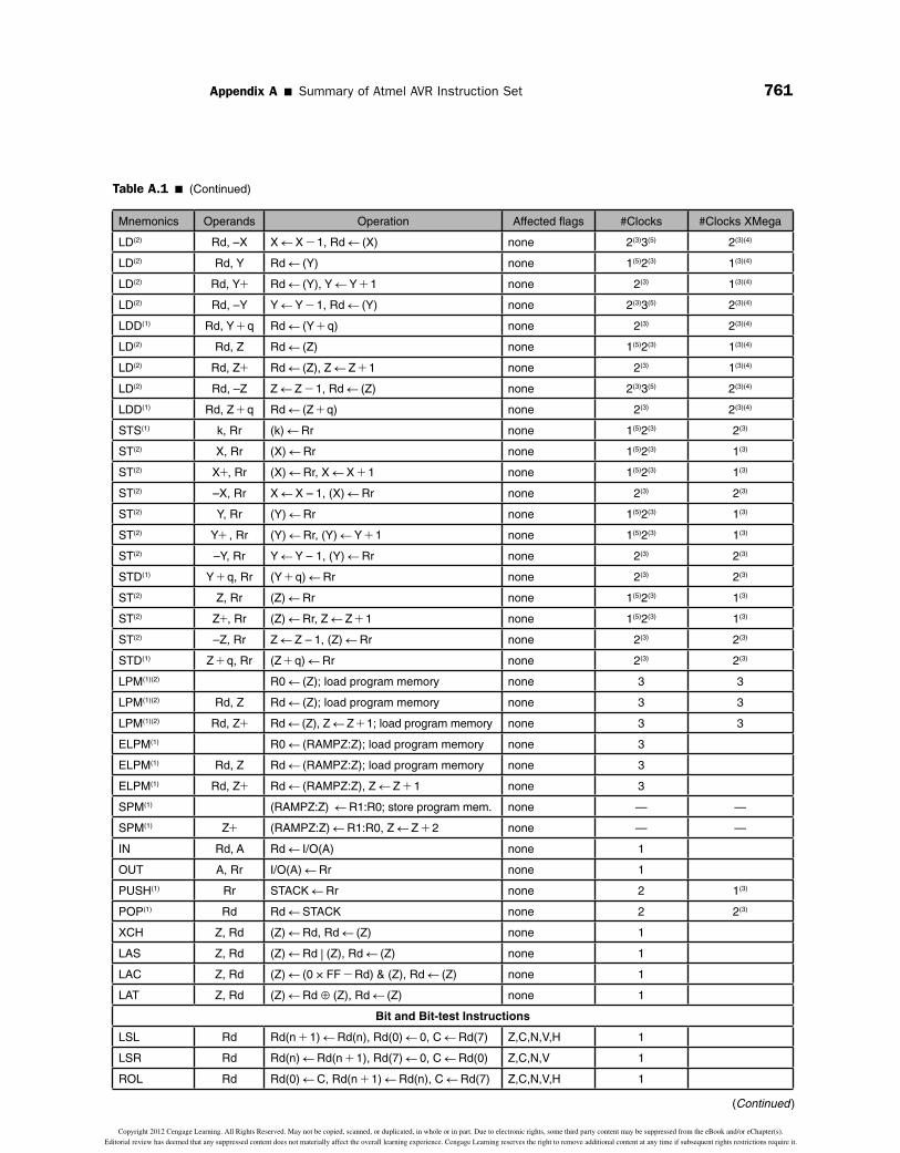
LDS(1) Rd, k Rd d (k) none 1(5)2(3) 2(3)(4)
LD(2) Rd, X Rd d (X) none 1(5)2(3) 1(3)(4)
LD(2) Rd, X+ Rd d (X), X d X + 1 none 2(3) 1(3)(4)
Table A.1 ■ (Continued)
07298_app_A_ptg01_hr_759-762.indd 76007298_app_A_ptg01_hr_759-762.indd 760 22/10/12 2:54 PM22/10/12 2:54 PM
Copyright 2012 Cengage Learning. All Rights Reserved. May not be copied, scanned, or duplicated, in whole or in part. Due to electronic rights, some third party content may be suppressed from the eBook and/or eChapter(s).
Editorial review has deemed that any suppressed content does not materially affect the overall learning experience. Cengage Learning reserves the right to remove additional content at any time if subsequent rights restrictions require it.
Appendix A ■ Summary of Atmel AVR Instruction Set 761
Mnemonics Operands Operation Affected flags #Clocks #Clocks XMega
LD(2) Rd, –X X d X - 1, Rd d (X) none 2(3)3(5) 2(3)(4)
LD(2) Rd, Y Rd d (Y) none 1(5)2(3) 1(3)(4)
LD(2) Rd, Y+ Rd d (Y), Y d Y + 1 none 2(3) 1(3)(4)
LD(2) Rd, –Y Y d Y - 1, Rd d (Y) none 2(3)3(5) 2(3)(4)
LDD(1) Rd, Y + q Rd d (Y + q) none 2(3) 2(3)(4)
LD(2) Rd, Z Rd d (Z) none 1(5)2(3) 1(3)(4)
LD(2) Rd, Z+ Rd d (Z), Z d Z + 1 none 2(3) 1(3)(4)
LD(2) Rd, –Z Z d Z - 1, Rd d (Z) none 2(3)3(5) 2(3)(4)
LDD(1) Rd, Z + q Rd d (Z + q) none 2(3) 2(3)(4)
STS(1) k, Rr (k) d Rr none 1(5)2(3) 2(3)
ST(2) X, Rr (X) d Rr none 1(5)2(3) 1(3)
ST(2) X+, Rr (X) d Rr, X d X + 1 none 1(5)2(3) 1(3)
ST(2) –X, Rr X d X – 1, (X) d Rr none 2(3) 2(3)
ST(2) Y, Rr (Y) d Rr none 1(5)2(3) 1(3)
ST(2) Y+ , Rr (Y) d Rr, (Y) d Y + 1 none 1(5)2(3) 1(3)
ST(2) –Y, Rr Y d Y – 1, (Y) d Rr none 2(3) 2(3)
STD(1) Y + q, Rr (Y + q) d Rr none 2(3) 2(3)
ST(2) Z, Rr (Z) d Rr none 1(5)2(3) 1(3)
ST(2) Z+, Rr (Z) d Rr, Z d Z + 1 none 1(5)2(3) 1(3)
ST(2) –Z, Rr Z d Z – 1, (Z) d Rr none 2(3) 2(3)
STD(1) Z + q, Rr (Z + q) d Rr none 2(3) 2(3)
LPM(1)(2) R0 d (Z); load program memory none 3 3
LPM(1)(2) Rd, Z Rd d (Z); load program memory none 3 3
LPM(1)(2) Rd, Z+ Rd d (Z), Z d Z + 1; load program memory none 3 3
ELPM(1) R0 d (RAMPZ:Z); load program memory none 3
ELPM(1) Rd, Z Rd d (RAMPZ:Z); load program memory none 3
ELPM(1) Rd, Z+ Rd d (RAMPZ:Z), Z d Z + 1 none 3
SPM(1) (RAMPZ:Z) d R1:R0; store program mem. none — —
SPM(1) Z+ (RAMPZ:Z) d R1:R0, Z d Z + 2 none — —
IN Rd, A Rd d I/O(A) none 1
OUT A, Rr I/O(A) d Rr none 1
PUSH(1) Rr STACK d Rr none 2 1(3)
POP(1) Rd Rd d STACK none 2 2(3)
XCH Z, Rd (Z) d Rd, Rd d (Z) none 1
LAS Z, Rd (Z) d Rd | (Z), Rd d (Z) none 1
LAC Z, Rd (Z) d (0 × FF - Rd) & (Z), Rd d (Z) none 1
LAT Z, Rd (Z) d Rd ⊕ (Z), Rd d (Z) none 1
Bit and Bit-test Instructions
LSL Rd Rd(n + 1) d Rd(n), Rd(0) d 0, C d Rd(7) Z,C,N,V,H 1
LSR Rd Rd(n) d Rd(n + 1), Rd(7) d 0, C d Rd(0) Z,C,N,V 1
ROL Rd Rd(0) d C, Rd(n + 1) d Rd(n), C d Rd(7) Z,C,N,V,H 1
Table A.1 ■ (Continued)
(Continued )
07298_app_A_ptg01_hr_759-762.indd 76107298_app_A_ptg01_hr_759-762.indd 761 22/10/12 2:54 PM22/10/12 2:54 PM
Copyright 2012 Cengage Learning. All Rights Reserved. May not be copied, scanned, or duplicated, in whole or in part. Due to electronic rights, some third party content may be suppressed from the eBook and/or eChapter(s).
Editorial review has deemed that any suppressed content does not materially affect the overall learning experience. Cengage Learning reserves the right to remove additional content at any time if subsequent rights restrictions require it.

762 Appendix A ■ Summary of Atmel AVR Instruction Set
Table A.1 ■ (Continued)
Mnemonics Operands Operation Affected flags #Clocks #Clocks XMega
ROR Rd Rd(7) d C, Rd(n) d Rd(n + 1), C d Rd(0) Z,C,N,V 1
ASR Rd Rd(n) d Rd(n + 1), n = 0, …, 6, Rd(7) d Rd(7) Z,C,N,V 1
SWAP Rd Rd(3..0) ↔ Rd(7..4) none 1
BSET s SREG(s) d 1 SREG(s) 1
BCLR s SREG(s) d 0 SREG(s) 1
SBI A, b I/O(A,b) d 1 none 1(5)2 1
CBI A, b I/O(A,b) d 0 none 1(5)2 1
BST Rr, b T d Rr(b) T 1
BLD Rd, b Rd(b) d T none 1
SEC C d 1 C 1
CLC C d 0 C 1
SEN N d 1 N 1
CLN N d 0 N 1
SEZ Z d 1 Z 1
CLZ Z d 0 Z 1
SEI I d 1 I 1
CLI I d 0 I 1
SES S d 1 S 1
CLS S d 0 S 1
SEV V d 1 V 1
CLV V d 0 V 1
SET T d 1 T 1
CLT T d 0 T 1
SEH H d 1 H 1
CLH H d 0 H 1
MCU Control Instructions
BREAK See specific description for BREAK none 1
NOP none 1
SLEEP See specific description about SLEEP none 1
WDR See specific description about WDR none 1
Note: 1. This instruction is not available in all devices. Refer to the device specific instruction set summary. 2. Not all variants of this instruction are available in all devices. Refer to the device specific set summary. 3. Cycle times for data memory accesses assume internal memory accesses, and are not valid for accesses via the
external RAM interface. 4. One extra cycle must be added when accessing internal SRAM. 5. Number of clock cycles for reduced core tinyAVR.
Source: Atmel Corporation, The Atmel AVR Microcontroller
07298_app_A_ptg01_hr_759-762.indd 76207298_app_A_ptg01_hr_759-762.indd 762 22/10/12 2:54 PM22/10/12 2:54 PM
Copyright 2012 Cengage Learning. All Rights Reserved. May not be copied, scanned, or duplicated, in whole or in part. Due to electronic rights, some third party content may be suppressed from the eBook and/or eChapter(s).
Editorial review has deemed that any suppressed content does not materially affect the overall learning experience. Cengage Learning reserves the right to remove additional content at any time if subsequent rights restrictions require it.

Electrical and Computer Engineering Dalhousie University
ECED3204: Microprocessor
Formula
Jason J. GuDepartment of Electrical and Computer Engineering
Dalhousie University
1
Electrical and Computer Engineering Dalhousie University
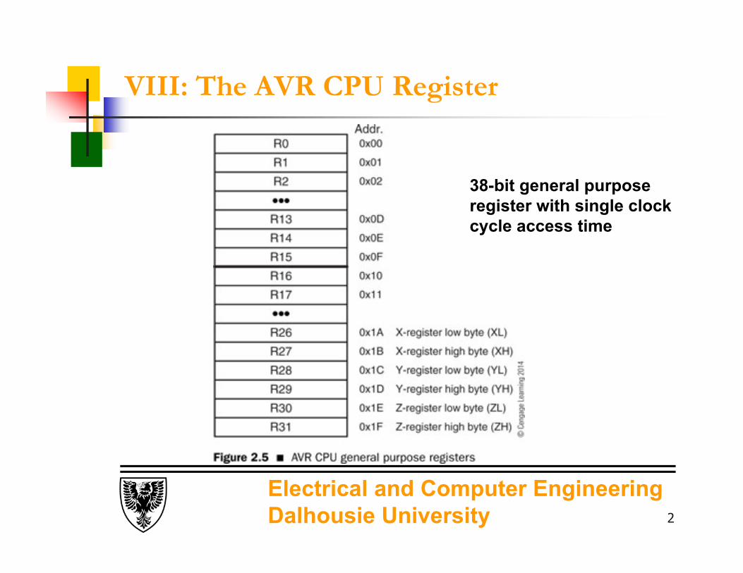
VIII: The AVR CPU Register
2
38-bit general purpose register with single clock cycle access time

Electrical and Computer Engineering Dalhousie University
Figure 2.9 The SREG register
I: Global interrupt enable flag, chapter 9T: Bit copy storageH: Half carry flagS: Sign bit
V: Two’s complement overflow flagN: Negative flagZ: Zero flagC: Carry flag
3

Electrical and Computer Engineering Dalhousie University 4
Assembler Directives
Table 3.2 AVR assembler directives
4

Electrical and Computer Engineering Dalhousie University 5
Assembler Directives (cont’d.)
Table 3.2 AVR assembler directives (cont’d.)
5

Electrical and Computer Engineering Dalhousie University
Overview of the AVR Mega Parallel PORTs
AVR Mega MCU may have 11 parallel ports
6
Note: No PORT I
Electrical and Computer Engineering Dalhousie University
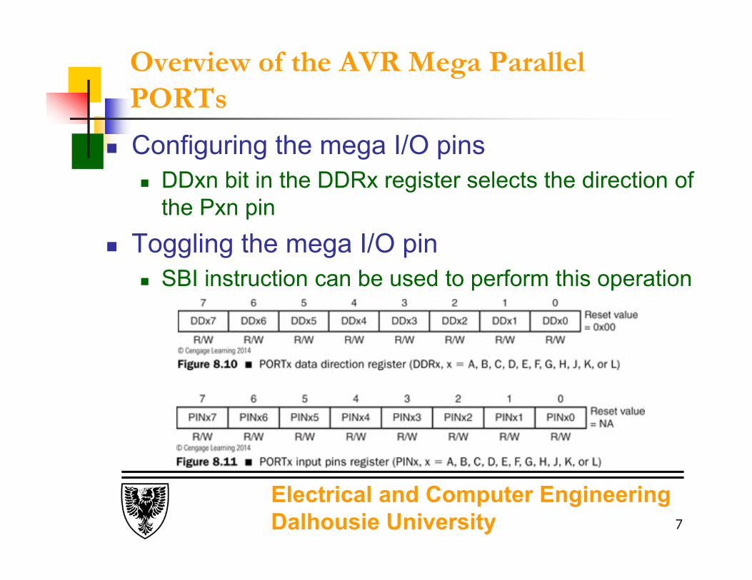
Overview of the AVR Mega Parallel PORTs
Configuring the mega I/O pins DDxn bit in the DDRx register selects the direction of
the Pxn pin Toggling the mega I/O pin
SBI instruction can be used to perform this operation
7

Electrical and Computer Engineering Dalhousie University
Simple I/O Devices Interfacing with seven-segment displays:
decoder
8

Electrical and Computer Engineering Dalhousie University
The AVR Mega Interrupts
9

Electrical and Computer Engineering Dalhousie University
The AVR Mega Interrupts
10

Electrical and Computer Engineering Dalhousie University
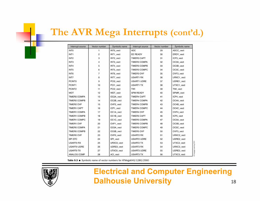
The AVR Mega Interrupts (cont’d.)
The Mega AVR microcontroller configuration register (MCUCR): controls interrupt vectors placement; controls enabling of I/O pins pull-up and the JTAG interface
11

Electrical and Computer Engineering Dalhousie University
The AVR Mega Interrupts (cont’d.)
AVR Mega external interrupt pins INT7:0 pins trigger interrupt requests to the MCU; pins
shared with PORTD (0-3) and E (4-7), controlled by EICRA and EICRB register.
12

Electrical and Computer Engineering Dalhousie University
The AVR Mega Interrupts (cont’d.)
13

Electrical and Computer Engineering Dalhousie University
The AVR Mega Interrupts (cont’d.)
EIMSK to enable the interrupt and EIFR to flag the interrupt.
14

Electrical and Computer Engineering Dalhousie University
The AVR Mega Interrupts (cont’d.)
15

Electrical and Computer Engineering Dalhousie University
The AVR Mega Interrupts (cont’d.)
16

Electrical and Computer Engineering Dalhousie University
The AVR Mega Interrupts (cont’d.)
17
Electrical and Computer Engineering Dalhousie University
The AVR Mega Interrupts (cont’d.)
18

Electrical and Computer Engineering Dalhousie University
Driving the Stepper Motor (cont’d.)
19

Electrical and Computer Engineering Dalhousie University
Driving the Stepper Motor (cont’d.)
20