application note 74 reading and writing ibuttons …application note 74 reading and writing ibuttons...
TRANSCRIPT
Application Note 74Reading and Writing iButtons
via Serial Interfaces
APPLICATION NOTE 74
102698 1/40
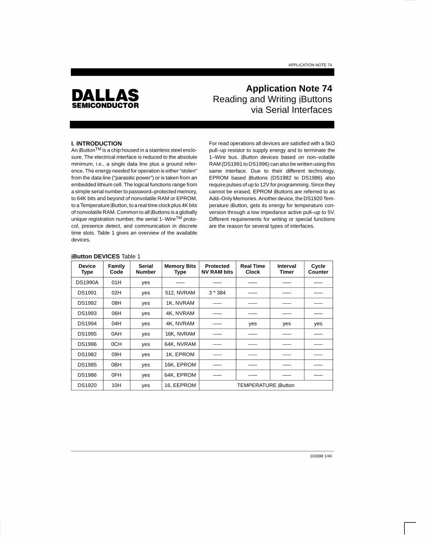
I. INTRODUCTIONAn iButtonTM is a chip housed in a stainless steel enclo-sure. The electrical interface is reduced to the absoluteminimum, i.e., a single data line plus a ground refer-ence. The energy needed for operation is either “stolen”from the data line (“parasitic power”) or is taken from anembedded lithium cell. The logical functions range froma simple serial number to password–protected memory,to 64K bits and beyond of nonvolatile RAM or EPROM,to a Temperature iButton, to a real time clock plus 4K bitsof nonvolatile RAM. Common to all iButtons is a globallyunique registration number, the serial 1–WireTM proto-col, presence detect, and communication in discretetime slots. Table 1 gives an overview of the availabledevices.
For read operations all devices are satisfied with a 5kΩpull–up resistor to supply energy and to terminate the1–Wire bus. iButton devices based on non–volatileRAM (DS1991 to DS1996) can also be written using thissame interface. Due to their different technology,EPROM based iButtons (DS1982 to DS1986) alsorequire pulses of up to 12V for programming. Since theycannot be erased, EPROM iButtons are referred to asAdd–Only Memories. Another device, the DS1920 Tem-perature iButton, gets its energy for temperature con-version through a low impedance active pull–up to 5V.Different requirements for writing or special functionsare the reason for several types of interfaces.
iButton DEVICES Table 1
Device Family Serial Memory Bits Protected Real Time Interval CycleDeviceType
FamilyCode
SerialNumber
Memory BitsType
ProtectedNV RAM bits
Real TimeClock
IntervalTimer
CycleCounter
DS1990A 01H yes ––– ––– ––– ––– –––
DS1991 02H yes 512, NVRAM 3 * 384 ––– ––– –––
DS1992 08H yes 1K, NVRAM ––– ––– ––– –––
DS1993 06H yes 4K, NVRAM ––– ––– ––– –––
DS1994 04H yes 4K, NVRAM ––– yes yes yes
DS1995 0AH yes 16K, NVRAM ––– ––– ––– –––
DS1996 0CH yes 64K, NVRAM ––– ––– ––– –––
DS1982 09H yes 1K, EPROM ––– ––– ––– –––
DS1985 0BH yes 16K, EPROM ––– ––– ––– –––
DS1986 0FH yes 64K, EPROM ––– ––– ––– –––
DS1920 10H yes 16, EEPROM TEMPERATURE iButton

APPLICATION NOTE 74
102698 2/40
II. 1–WIRE INTERFACEA. General InformationiButtons are self–timed silicon devices. The timing logicprovides a means of measuring and generating digitalpulses of various widths. Data transfers are bit–sequen-tial and half–duplex. Data can be interpreted as com-mands (according to the prearranged format identified bythe family code) that are compared to information alreadystored in the iButton to make a decision, or can simply bestored in the iButton for later retrieval. iButtons are con-sidered slaves, while the host reader/writer is considereda master.
B. DC RequirementsiButtons operate in an open drain environment on volt-age levels ranging from 2.8V (minimum pull–up voltage)to 6V (maximum pull–up voltage). All voltages greaterthan 2.2V are interpreted as logic 1 or HIGH, voltagesless than 0.8V are considered as logic 0 or LOW. Thepull–up voltage must be a minimum of 2.8V to rechargean internal storage capacitor that is used to supplypower during periods when the data line is low. The sizeof this capacitor is about 800 pF. This capacity is seenfor a short time when an iButton is contacted by a probe.After the capacitor is charged, only a very small fractionof this capacity is recognizable, according to the chargerequired to refill to full charge. The total time constant tocharge the capacitor is defined by the capacitor itself, theinternal resistances of about 1 kΩ, the resistance of thecable and contacts, the cable capacitance, and the resis-tor pulling up the data line.
C. AC RequirementsTiming relationships in iButtons are defined with respectto time slots. Because the falling slope is the least sensi-tive to capacitive loading in an open drain environment,iButtons use this edge to synchronize their internal tim-ing circuitry. By definition the active part of a 1–Wire timeslot (tSLOT) is 60 µs. After the active part of the time slot,the data line needs to be inactive for a minimum of 1 µs
at a voltage of 2.8V or higher to recharge the internalcapacitor.
Under nominal conditions, an iButton will sample theline 30 µs after the falling edge of the start condition. Theinternal time base of iButton may deviate from its nomi-nal value. The allowed tolerance band ranges from 15µs to 60 µs. This means that the actual slave samplingmay occur anywhere between 15 and 60 µs after thestart condition, which is a ratio of 1 to 4. During this timeframe the voltage on the data line must stay belowVILMAX or above VIHMIN.
C.1. Write Time SlotsIn the 1–Wire system, the logical values of 1 and 0 arerepresented by certain voltage levels in special wave-forms. The waveforms needed to write commands ordata to iButtons are called write–1 and write–0 timeslots. The duration of a low pulse to write a 1 (tLOW1, Fig-ure 1 ) must be shorter than 15 µs. To write a 0, the dura-tion of the low pulse (tLOW0, Figure 2) must be at least 60µs to cope with worst–case conditions.
The duration of the active part of a time slot can beextended beyond 60 µs. The maximum extension is lim-ited by the fact that a low pulse of a duration of at leasteight active time slots (480 µs) is defined as a ResetPulse. Allowing the same worst–case tolerance ratio, alow pulse of 120 µs might be sufficient for a reset. This lim-its the extension of the active part of a time slot to a maxi-mum of 120 µs to prevent misinterpretation with reset.
At the end of the active part of each time slot, iButtonneeds a recovery time tREC of a minimum of 1 µs to pre-pare for the next bit. This recovery time is the inactivepart of a time slot, since it must be added to the durationof the active part to obtain the time it takes to transferone bit. The wide tolerance of the time slots and thenon–critical recovery time allow even slow micropro-cessors to meet the timing requirements for 1–Wirecommunication easily.

APPLICATION NOTE 74
102698 3/40
WRITE–ONE TIME SLOT Figure 1
60 µs
tREC
tLOW1
VPULLUPVPULLUP MIN
VIH MIN
VIL MAX0V
60 µs < tSLOT < 120 µs
1 µs < tLOW1 < 15 µs
1 µs < tREC <
15 µs
SAMPLING WINDOW
tSLOT
RESISTOR
MASTER
iButton
iButton
WRITE–ZERO TIME SLOT Figure 2
VPULLUPVPULLUP MIN
VIH MIN
VIL MAX0V
RESISTOR
MASTER
tSLOT
tREC
tLOW0
60 µs < tLOW0 < tSLOT < 120 µs
1 µs < tREC <
SAMPLING WINDOW
60 µs
15 µs
iButton
iButton
APPLICATION NOTE 74
102698 4/40
C.2. Read Time SlotsCommands and data are sent to iButtons by combiningWrite–Zero and Write–One time slots. To read data, themaster has to generate Read–Data time slots to definethe start condition of each bit. The Read–Data time slotlooks essentially the same as the Write–One time slotfrom the master’s point of view. Starting at the high–to–low transition, the iButton sends one bit of its addressedcontents. If the data bit is a 1, the iButton leaves thepulse unchanged. If the data bit is a 0, the iButon will pullthe data line low for tRDV or 15 µs (Figure 3). In this timeframe data is valid for reading by the master. The dura-tion tLOWR of the low pulse sent by the master should bea minimum of 1 µs with a maximum value as short aspossible to maximize the master sampling window. Inorder to compensate for the cable capacitance of the1–Wire line the master should sample as close to 15 µsafter the synchronization edge as possible. FollowingtRDV there is an additional time interval, tRELEASE, afterwhich the iButton releases the 1–Wire line so that itsvoltage can return to VPULLUP. The duration of tRELEASEmay vary from 0 to 45 µs; its nominal value is 15 µs.
C.3. Reset and Presence DetectThe Reset Pulse provides a clear starting condition thatsupersedes any time slot synchronization. It is definedas a single low pulse of minimum duration of eight timeslots or 480 µs followed by a Reset–high time tRSTH ofanother 480 µs (Figure 4). After a Reset Pulse has beensent, the iButton will wait for the time tPDH and then gen-erate a Presence Pulse of duration tPDL. No other com-munication on the 1–Wire bus is allowed during tRSTH.The Presence Pulse can be used to trigger a hardwareinterrupt or to automatically power up equipment likeTouch Pens. If an iButton is disconnected from the
probe, it will pull its data line low via an internal currentsource of 5 µA. This simulates a Reset Pulse of unlim-ited duration. As soon as the iButton detects a high levelon the data line, it will generate a Presence Pulse.
The nominal values are 30 µs for tPDH and 120 µs fortPDL. With the same worst–case tolerance band, themeasured tPDH value indicates the internal time base ofthe fastest device. The sum of the measured tPDH andtPDL values is five times the internal time base of theslowest device. If there is only one device on the line,both values will deviate in the same direction. This cor-relation can be used to build an adaptive system. Spe-cial care must be taken to recalibrate timing after everyreset since the individual timing characteristics of thedevices vary with temperature and load.
The accuracy of the time measurements required foradaptive timing is limited by the characteristics of themaster’s input logic, the time constant of the 1–Wire line(pullup resistor x cable capacitance) and the appliedsampling rate. If the observed rise time or fall timeexceeds 1 µs or the highest possible sampling rate isless than 1 MHz, adaptive timing should not beattempted.
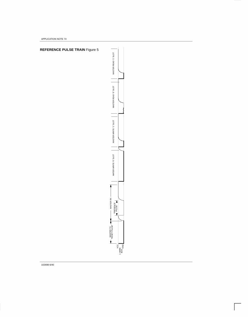
C.4. Example Pulse TrainFor illustrative purposes, a reference pulse train hasbeen defined (Figure 5) to explain how the waveformsare generated rather than showing a complete session.It starts with a reset sequence including a PresencePulse. Further time slots show all waveforms of readingand writing 1s and 0s. Any communication session canbe constructed from the waveforms of this pulse train.

APPLICATION NOTE 74
102698 5/40
READ–DATA TIME SLOT Figure 3
VPULLUPVPULLUP MIN
VIH MIN
VIL MAX0V
tSLOT tREC
tRDV
tLOWR
60 µs < tSLOT < 120 µs
1 µs < tLOWR < 15 µs
0 < tRELEASE < 45 µs
1 µs < tREC <
tRDV = 15 µs
tRELEASE
MASTER SAMPLINGWINDOW
RESISTOR
MASTER
iButton
RESET AND PRESENCE PULSE Figure 4tRSTH
tRSTLtR
VPULLUPVPULLUP MIN
VIH MIN
VIL MAX0V
480 µs < tRSTL < *
480 µs < tRSTH < (includes recovery time)
15 µs < tPDH < 60 µs
60 µs < tPDL < 240 µs
tPDH
tPDL
RESISTOR
MASTER
iButton
* In order not to mask interrupt signalling by other devices on the 1–Wire bus, tRSTL + tR should always be less than 960 µs.
MA
TE
R W
RIT
E “
0” S
LOT
MA
ST
ER
WR
ITE
“1”
SLO
TM
AS
TE
R R
EA
D “
0” S
LOT
MA
ST
ER
RE
AD
“1”
SLO
T
MA
ST
ER
TX
MA
ST
ER
RX
GN
D
VC
C1–
WIR
E
“RE
SE
T P
ULS
E”
“PR
ES
EN
CE
PU
LSE
”
BU
S
APPLICATION NOTE 74
102698 6/40
REFERENCE PULSE TRAIN Figure 5
APPLICATION NOTE 74
102698 7/40
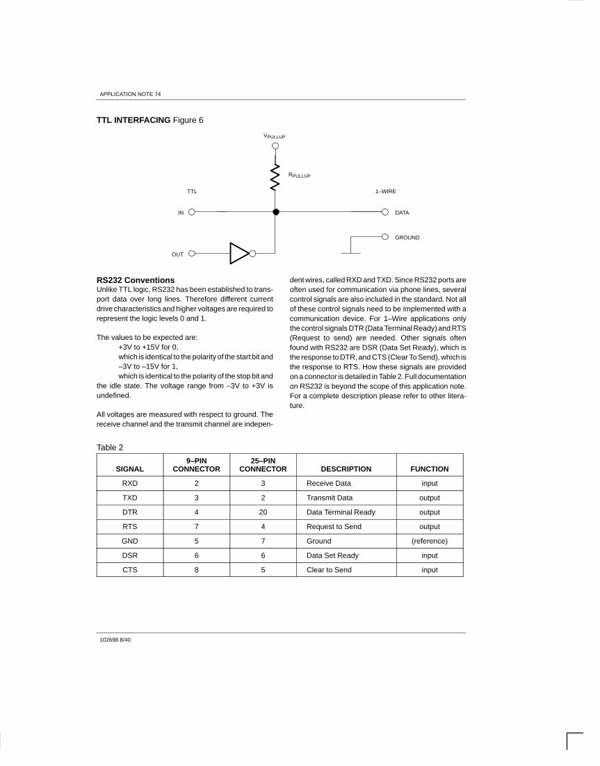
III. FUNDAMENTALSA. TTL InterfaceThis category includes all logic families and micropro-cessors that use positive logic with a maximum 0.8V fora logical 0 or LOW and a minimum of 2.2V for a logical 1or HIGH. These voltages combined with a currentsource capability of at least 1 mA and a sink capability ofmore than 4 mA interface to a broad class of digital elec-tronics.
Since the 1–Wire bus is an open drain system, an opendrain/collector driver is required to connect the outputport to the bus (Figure 6). This driver can be a generalpurpose NPN transistor with a resistor connectedbetween base and output port or an n–channel MOS-FET or any open drain/collector driver available in thelogic family as long as the pullup voltage is equal to thedriver voltage. Even a tri–state driver with its logic inputtied to ground can be used, connecting the output gateto the tri–state control input. Depending on the charac-teristics of the driver (inverting/non–inverting), it may berequired to complement the logic value of the outputgate to compensate for the driver’s signal inversion.
Reading from the 1–Wire bus can usually be accom-plished by directly connecting the 1–Wire bus to theinput port of the master. If the pullup–voltage of the1–wire bus is too low or if the capacity of the cable pro-duces slopes too slow for the logic family, it may berequired to employ a comparator as interface and toadjust the reference voltage to optimize noise marginsand timing characteristics. If the comparator inverts thesignal, this inversion needs to be compensated by thesoftware.
Generally it is recommended to test this type of interfacecarefully, starting with reset pulses generated by soft-ware and watching the slopes with an oscilloscope. Ifthe timing specifications of Figure 4 are met, and thepresence pulse is seen, one may proceed and test thesoftware to generate the Write–Zero and Write–Onetime slots. After this works properly, the next step isreading the ROM. This is done by performing a resetcycle first, followed by 2 Write–One time slots, 2 Write–Zero time slots, 2 Write–One time slots and 2 Write–Zero time slots (this is equivalent to sending 33H, leastsignificant bit first). After this, 64 Read Data time slotsneed to be generated.
Since all timing depends on the clock frequency of themicrocontroller, it is required to count the number ofclock cycles for the execution of each command withinthe loop. The level of an output pin of a microprocessorwill usually not change at the end of a command, but afew clock cycles earlier. The actual reading from anyinput pin also occurs some clock cycles before the endof the command. If the description of the microproces-sor does not give sufficient details on this, a test serieswith different clock frequencies may be required. Aslong as the microprocessor is executing time–sensitivecode, i.e., reading from the 1–Wire bus or writing to it,jumps or calls may occur only while the 1–Wire bus isidle. Interrupts from other sources than the 1–Wire busmust be disabled.
B. RS232 InterfaceThis section covers all interfaces that use a special con-troller to generate all timing and reference signalsrequired for serial communication. The typical controllerfor this type of interface is the UART 8250. It relieves themicroprocessor of the burden of time–critical softwareexecution. The microprocessor simply puts the charac-ter code to be transmitted into the transmit register of theUART and the UART will do the work. A character isreceived by the microprocessor just by reading theUART’s receive register. If the serial transmission is fin-ished or if there is data for the microprocessor, thiscondition is signalled by the UART through flags thatcan be polled or by interrupts.
To function properly, the UART requires configurationwith respect to baud rate, number of data bits per char-acter, parity and number of start and stop bits. Theseterms are common for serial communication, but fit theneeds of 1–Wire networks with their time slots and sep-arate synchronization if a bit rather than a character isframed by the start condition. For 1–Wire communica-tion the UART is set up for a high baud rate and eachcharacter delivered by the UART represents a bit on the1–Wire bus. The microprocessor must separate the bitsof a byte, least significant bit first, and write them asappropriate characters to the UART. To read data, themicroprocessor has to assemble the bits receivedthrough characters back into bytes. These functions arenot time–sensitive and can easily be programmed in ahigh level language.
APPLICATION NOTE 74
102698 8/40
TTL INTERFACING Figure 6
IN
OUT
VPULLUP
RPULLUP
DATA
GROUND
1–WIRETTL
RS232 ConventionsUnlike TTL logic, RS232 has been established to trans-port data over long lines. Therefore different currentdrive characteristics and higher voltages are required torepresent the logic levels 0 and 1.
The values to be expected are:+3V to +15V for 0, which is identical to the polarity of the start bit and–3V to –15V for 1, which is identical to the polarity of the stop bit and
the idle state. The voltage range from –3V to +3V isundefined.
All voltages are measured with respect to ground. Thereceive channel and the transmit channel are indepen-
dent wires, called RXD and TXD. Since RS232 ports areoften used for communication via phone lines, severalcontrol signals are also included in the standard. Not allof these control signals need to be implemented with acommunication device. For 1–Wire applications onlythe control signals DTR (Data Terminal Ready) and RTS(Request to send) are needed. Other signals oftenfound with RS232 are DSR (Data Set Ready), which isthe response to DTR, and CTS (Clear To Send), which isthe response to RTS. How these signals are providedon a connector is detailed in Table 2. Full documentationon RS232 is beyond the scope of this application note.For a complete description please refer to other litera-ture.
Table 2
SIGNAL9–PIN
CONNECTOR25–PIN
CONNECTOR DESCRIPTION FUNCTION
RXD 2 3 Receive Data input
TXD 3 2 Transmit Data output
DTR 4 20 Data Terminal Ready output
RTS 7 4 Request to Send output
GND 5 7 Ground (reference)
DSR 6 6 Data Set Ready input
CTS 8 5 Clear to Send input

APPLICATION NOTE 74
102698 9/40
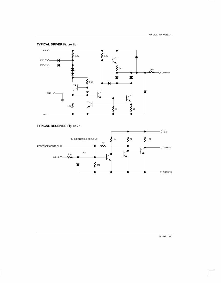
Hardware Simplified ModelThe standard hardware of a RS232 interface is shown inFigure 7a. The UART is hooked to the system bus likean 8–bit memory device. The three address inputs A0 toA2 make the UART appear as a block of 8 read/writememory locations. On the other side there are the serialcommunication signals and the control signals men-tioned above. Since the UART is a 5V device, specialdrivers and receivers for handling higher voltages arerequired. Circuit diagrams of bipolar integrated drivers(1488) and receivers (1489) are shown on Figures 7band 7c. CMOS drivers and receivers are also availableas standard products.
By design, the output current of an RS232 driver is lim-ited to ±10 mA typically. Since the voltage definitions for1 and 0 on the RS232 channel are reversed with respectto the conventions of positive logic, RS232 drivers andreceivers are actually inverting devices. The inversionin the transmit channel is compensated through aninversion in the receive channel. Thus a 1 written to thetransmit register will appear as a 1 at the serial output,as –15V at TXD, as a 1 at the serial input of the receiverand finally be read as a 1 in the receive register of thereceiving UART.
For energy efficiency with battery operated equipment,the RS232 drivers and receivers are often replaced bysimple 5V inverting drivers. This is definitely not com-patible with the RS232 standard, but may be sufficient tocontrol a modem or to transfer data through a shortcable. Interfaces like this are called 5V RS232 withinthis application note. They run on the same software asthe standard RS232, but are electrically almost thesame as the TTL interface.
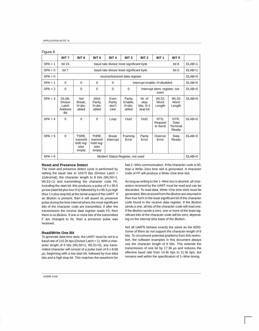
Programmer’s ModelTo write software for the 8250 UART one must know thebasic address where the registers of the UART arehardwired to. This address is generally an equipmentspecific variable, and therefore will be referenced by thename SPA (Serial Port Address) rather than by a physi-cal address. Of the 8 theoretically accessible addresseswithin the UART only 7 are really implemented, usingthe relative addresses 0 to 6. The names of these regis-ters are as follows:
address:SPA +0 Receive (read)/Transmit (write)
Data Register
+1 Interrupt Enable Register+2 Interrupt Identification Register
(read only)+3 Line Control Register+4 Modem Control Register+5 Line Status Register+6 Modem Status Register
The meaning of the UART’s control bits and their posi-tion within the control registers is detailed in Figure 8.For 1–Wire communication, the Interrupt IdentificationRegister and Modem Status Register are not used.
To define the speed or baud rate of a serial communica-tion, there is a 16 bit register, called Divisor Latch. Thisregister is accessed as two bytes using the sameaddresses as the Data Register (least significant byte)and the Interrupt Enable Register (most significantbyte). To access the Divisor Latch, the Divisor LatchAccess Bit DLAB must be set to 1. DLAB is the most sig-nificant bit of the Line Control Register. As long as DLABis set, the Data Register and the Interrupt Enable Regis-ter are not accessible. For the commonly used crystalfrequency of 1.8432 MHz, the divisor latch mustcontain a number between 2304 (900hex, 50 bps) and1 (115.2k bps).
1–Wire Communication through the UARTAs mentioned above, to write one bit to the 1–Wire bus,the UART is programmed to transmit one character.Since the receive and transmit channels of the UARTare operating independently, but using the same com-munication setup, reading from and writing to the1–Wire bus can occur at the same time. The start condi-tion generated at the UART’s serial output is fed to the1–Wire bus and is simultaneously returned to the serialinput, triggering the process of reading one character.The waveform is completely defined by the baud rate,the polarity of the start and stop bits and the bit pattern ofthe character. The serial output of the UART is high(~ 5V, idle) between characters, low (~0V) for the startbit and equal to the value of the data bit being trans-mitted. An idle (~5V) to low (~0V) transition at theUART’s serial input triggers the process of receiving acharacter. The first bit is understood as start bit; theremaining bits are shifted into the receive register in thesame polarity as they arrive at the serial input. Bitsreceived after the receive register is full, are ignored.

APPLICATION NOTE 74
102698 10/40
HARDWARE OVERALL CONCEPT Figure 7a
ADS
CS2
WR
RD
DCO
DSR
CTS
RI
OUT2
OUT1
RTS
DTR
BAUDOUT
16
17
15
9
33
32
34
31
39
38
37
36
11
10
30
24
23
29
RS–232CONNECTOR
20
4
8
6
2
3
7
1
DTR
RTS
DSR
CTS
TXD
RXD
GND
+5V
XIN
XOUT
RCLK
SOUT
SIN
INTR
CSOUT
DDIS
NC
A0–A2
CS0
CS1
D0–D7
MR
RD
WR
8250(UART)
20 40
12
13
21
18
35
22
19
25
14
GNDVSS
+5V(VCC)
5
APPLICATION NOTE 74
102698 11/40
TYPICAL DRIVER Figure 7b
GND
VCC
INPUT
INPUT
VEE
30070
707k
10k
3.6k
8.2k 6.2k
OUTPUT
TYPICAL RECEIVER Figure 7c
RESPONSE CONTROL
INPUT
VCC
OUTPUT
GROUND
10k
9k 5k 1.7k
3.8kRF
RF
RF IS EITHER 6.7 OR 1.6 kΩ
APPLICATION NOTE 74
102698 12/40
Figure 8
BIT 7 BIT 6 BIT 5 BIT 4 BIT 3 BIT 2 BIT 1 BIT 0
SPA + 1 bit 15 baud rate divisor most significant byte bit 8 DLAB=1
SPA + 0 bit 7 baud rate divisor least significant byte bit 0 DLAB=1
SPA + 0 receive/transmit data register DLAB=0
SPA + 1 0 0 0 0 Interrupt enable; 0=disabled DLAB=0
SPA + 2 0 0 0 0 0 Interrupt ident. register, notused
DLAB=0
SPA + 3 DLAB,DivisorLatch
AddressBit
SetBreak,0=dis-abled
StickParity,0=dis-abled
EvenParitydon’tcare
ParityEnable,0=dis-abled
Nr. ofstop
bits, 0=1stop bit
WLS1Word
Length
WLS0Word
Length
DLAB=0
SPA + 4 0 0 0 Loop Out2 Out1 RTS,Requestto Send
DTR,Data
TerminalReady
DLAB=0
SPA + 5 0 TSRE,transmitshift reg-
isterempty
THRE,transmithold reg-
isterempty
BreakInterrupt
FramingError
ParityError
OverrunError
DataReady
DLAB=0
SPA + 6 Modem Status Register, not used DLAB=0
Reset and Presence DetectThe reset and presence detect cycle is performed bysetting the baud rate to 10473 bps (Divisor Latch =11decimal), the character length to 8 bits (WLS0=1,WLS1=1) and transmitting the character code F0.Including the start bit, this produces a pulse of 5 x 95.5µs low (start bit plus four 0’s) followed by 5 x 95.5 µs high(four 1’s plus stop bit) at the serial output of the UART. Ifan iButton is present, then it will assert its presencepulse during the time interval where the most significantbits of the character code are transmitted. If after thetransmission the receive data register reads F0, thenthere is no iButton. If one or more bits of the transmittedF are changed to 0s, than a presence pulse wasreceived.
Read/Write One BitTo generate data time slots, the UART must be set to abaud rate of 115.2k bps (Divisor Latch = 1). With a char-acter length of 6 bits (WLS0=1, WLS1=0), any trans-mitted character will consist of a pulse train of 8 x 8.68µs, beginning with a low start bit, followed by true databits and a high stop bit. This matches the waveform for
fast 1–Wire communication. If the character code is 00,than a Write–Zero time slot is generated. A charactercode of FF will produce a Write–One time slot.
As long as writing to the 1–Wire bus is desired, all char-acters received by the UART must be read and can bediscarded. To read data, Write–One time slots must begenerated. Bits received from the iButton are returned intheir true form in the least significant bit of the charactercode found in the receive data register. If the iButtonsends a one, all bits of the character code will read one.If the iButton sends a zero, one or more of the least sig-nificant bits of the character code will be zero, depend-ing on the internal time base of the iButton.
Not all UARTs behave exactly the same as the 8250.Some of them do not support the character length of 6bits. To circumvent potential problems from this restric-tion, the software examples in this document alwaysuse the character length of 8 bits. This extends thetransmission of one bit by 17.36 µs and reduces theeffective baud rate from 14.4k bps to 11.5k bps, butremains well within the specification of 1–Wire timing.

APPLICATION NOTE 74
102698 13/40
IV. CIRCUITS FOR 5V INTERFACES (TTLAND RS232)A. TTL Read AllThis is the simplest interface for iButton applications. Itis suitable for reading all iButtons and writing NVRAMbased devices. The circuit diagram (Figure 9) conformsto the principle of Figure 6. The diodes D1 and D2 pro-tect transistor Q1 and the input of the microprocessor,respectively, against damage from electrostatic dis-charge (ESD). R1 is the 1–Wire pullup resistor. If themicroprocessor runs on 5V, the same supply candirectly be connected to R1. If only a higher supply volt-age than 5V is available, any monolithic or discrete posi-tive 5V regulator can be used to provide the pullup volt-age for the 1–Wire bus.
The characteristics of the components are not critical.The transistor 2N7000 has been chosen since it is avery common product and has a low threshold voltage.
If desired, a small signal bipolar transistor or any avail-able open–drain or open–collector inverting driver canbe used instead of Q1. If Q1 is an npn–transistor, aresistor bypassed by a small capacitor between the TX–input and the base terminal is required to limit the inputcurrent.
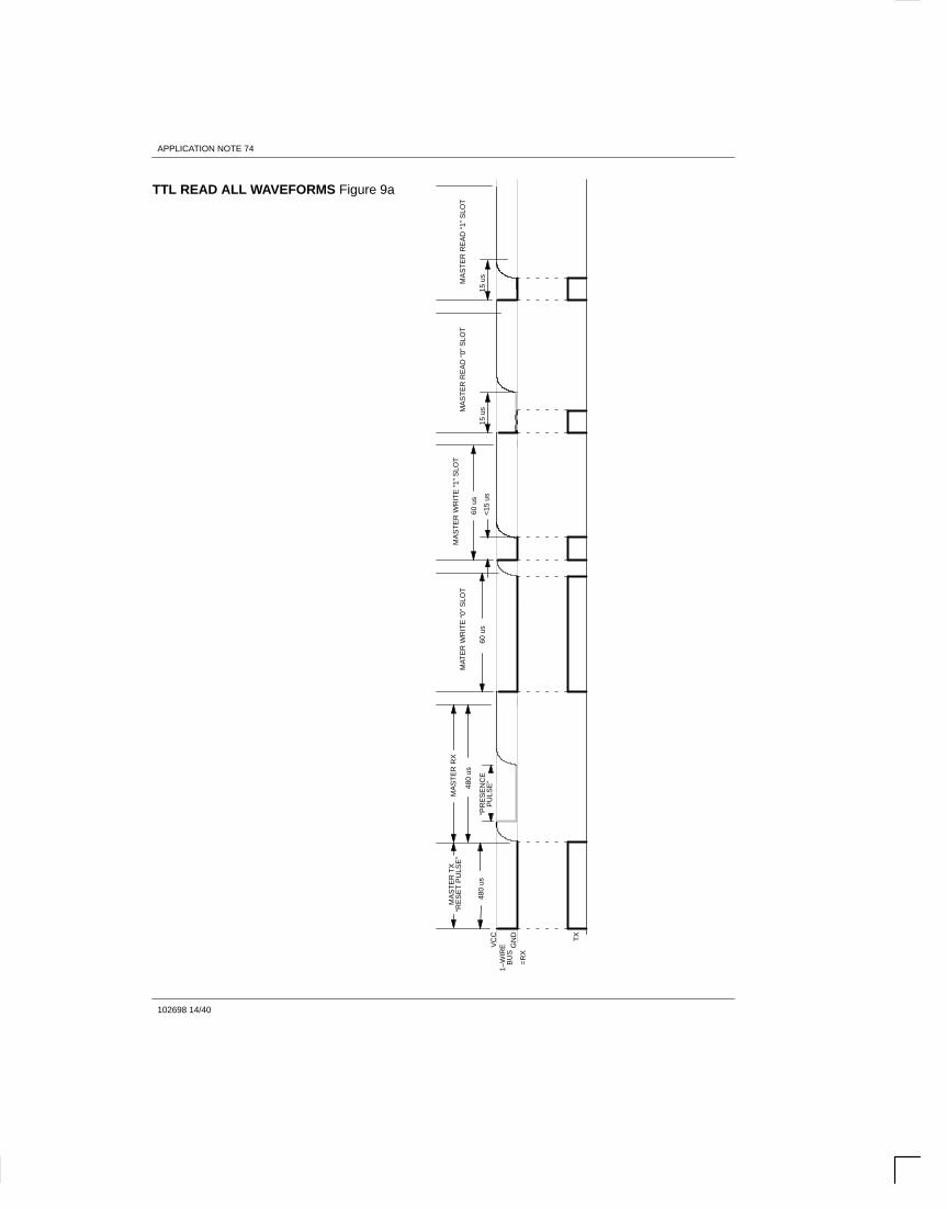
The logic level high at TX will produce a low on the1–Wire bus. To generate a Write–One or Read Datatime slot, a short high pulse (1 µs < t < 15 µs) must beapplied to the TX input. A Write–Zero Time Slot isformed by a 60 µs high pulse at TX. Data from iButtons isreceived in its true form. If idle, TX must be held at a logiclow level. The reference pulse train and other relevantwaveforms for this circuit are shown on Figure 9a. Thetiming for this type of interface is directly generated bythe microprocessor. A software example for this type ofinterface is found later in this document.
TTL READ ALL CIRCUIT Figure 9
D2D1
R14.7K
+5V
RXD
TXD
GND
1N524212V
1N52325.6V
MA
TE
R W
RIT
E “
0” S
LOT
MA
ST
ER
WR
ITE
“1”
SLO
TM
AS
TE
R R
EA
D “
0” S
LOT
MA
ST
ER
RE
AD
“1”
SLO
T
MA
ST
ER
TX
MA
ST
ER
RX
GN
D
VC
C1–
WIR
E
“RE
SE
T P
ULS
E”
“PR
ES
EN
CE
PU
LSE
”
BU
S
480
us
480
us
60 u
s60
us
<15
us
15 u
s15
us
TX
=R
X
APPLICATION NOTE 74
102698 14/40
TTL READ ALL WAVEFORMS Figure 9a
APPLICATION NOTE 74
102698 15/40
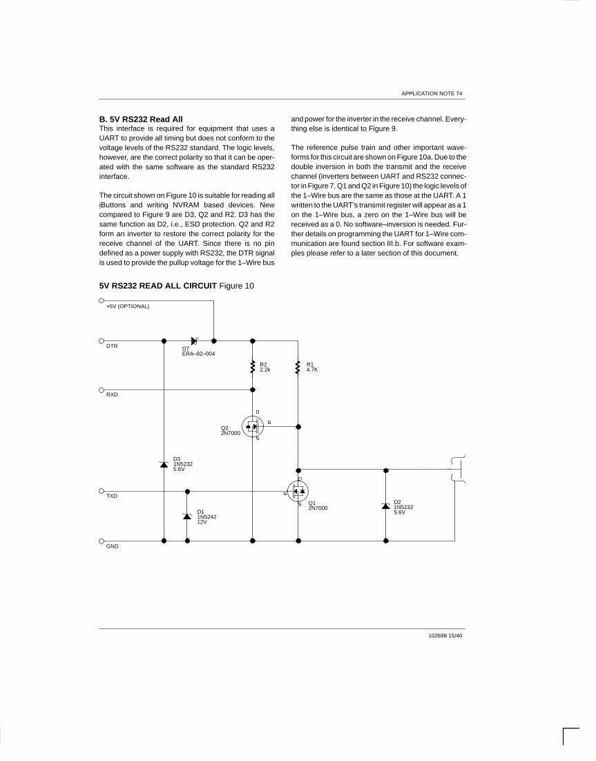
B. 5V RS232 Read AllThis interface is required for equipment that uses aUART to provide all timing but does not conform to thevoltage levels of the RS232 standard. The logic levels,however, are the correct polarity so that it can be oper-ated with the same software as the standard RS232interface.
The circuit shown on Figure 10 is suitable for reading alliButtons and writing NVRAM based devices. Newcompared to Figure 9 are D3, Q2 and R2. D3 has thesame function as D2, i.e., ESD protection. Q2 and R2form an inverter to restore the correct polarity for thereceive channel of the UART. Since there is no pindefined as a power supply with RS232, the DTR signalis used to provide the pullup voltage for the 1–Wire bus
and power for the inverter in the receive channel. Every-thing else is identical to Figure 9.
The reference pulse train and other important wave-forms for this circuit are shown on Figure 10a. Due to thedouble inversion in both the transmit and the receivechannel (inverters between UART and RS232 connec-tor in Figure 7, Q1 and Q2 in Figure 10) the logic levels ofthe 1–Wire bus are the same as those at the UART. A 1written to the UART’s transmit register will appear as a 1on the 1–Wire bus, a zero on the 1–Wire bus will bereceived as a 0. No software–inversion is needed. Fur-ther details on programming the UART for 1–Wire com-munication are found section III.b. For software exam-ples please refer to a later section of this document.
5V RS232 READ ALL CIRCUIT Figure 10
+5V (OPTIONAL)
DTR
RXD
TXD
GND
D7ERA–82–004
R22.2k
R14.7K
Q22N7000
D31N52325.6V
D11N524212V
Q12N7000
D21N52325.6V

TX
D
DT
R
RX
D
PC
–GN
D
ST
12
34
=1–
WIR
EG
ND
56
78
Sto
pS
T1
23
45
61
23
45
6S
top
Sto
pS
tart
12
34
56
Sto
pS
tart
12
34
56
Sto
pS
tart
(5V
)
0V
00
00
00
00
00
11
11
11
11
11
11
11
11
11
1
SE
ND
F0
HE
X10
473
BP
S8
DA
TA B
ITS
NO
PA
RIT
Y, 1
ST
OP
BIT
SE
ND
00
HE
X(6
BIT
S)
SE
ND
3F
HE
XS
EN
D 3
F H
EX
SE
ND
3F
HE
X
1152
00 B
PS
6 D
ATA
BIT
SN
O P
AR
ITY,
1 S
TO
P B
IT
MA
TE
R W
RIT
E “
0” S
LOT
MA
ST
ER
WR
ITE
“1”
SLO
TM
AS
TE
R R
EA
D “
0” S
LOT
MA
ST
ER
RE
AD
“1”
SLO
T
MA
ST
ER
TX
MA
ST
ER
RX
GN
D
VC
C1–
WIR
E
“RE
SE
T P
ULS
E”
“PR
ES
EN
CE
PU
LSE
”
BU
S
480
us
480
us
60 u
s60
us
<15
us
15 u
s15
us
11
11
APPLICATION NOTE 74
102698 16/40
5V RS232 READ ALL WAVEFORMS Figure 10a

APPLICATION NOTE 74
102698 17/40
C. TTL R/W All (Voltage Converter)The circuits described so far can read all iButtons andwrite NVRAM–based devices. For other technologies,however, voltage requirements other than 5V are nec-essary. One important group of iButtons, called Add–Only Memories, is based on EPROM technology andtherefore needs a programming pulse of 12V to copydata from the scratchpad to the EPROM cells. Anotherdevice, the Temperature iButton, will operate on 5V butrequires a low impedance pull–up to 5V while measur-ing the temperature. To fulfill the requirements of theseand future devices, the circuits described above need tobe upgraded. These two new functions require two
more signals and the 12V programming supply can beprovided by a DC–to–DC voltage converter.
The complete circuit of such a universal interface in aTTL–version is shown in Figure 11. It is a compatiblesuperset of Figure 9. The components Q1, R1, D1, D2and their functions are the same as before. Additionalrequirements include the control input PGMEN with thediode D4 for ESD protection, the diode D5, the cas-caded inverters R3, Q3, R4 and Q4 & R5, C1, thepull–up switch Q5 and the controlled voltage converterIC1 with its external components L1, D6 and C2.
TTL R/W ALL CIRCUIT Figure 11
b c
a
8
3
1
7
4
D
G
S
D
G
S
D
S
G
D
G
S
SHDN
+5V
PGMEN
RXD
TXD
GND
D11N5242
Q12N7000
D21N5242
Q42N7000Q3
2N7000
L1 D61N5818
D5ERA–82–004
R14.7K
R3R4100K
Q5BSS110
R547K
C210 uF
U1LT1109CN8–12
SW
GNDSHDN
VCC
D41N5242
C1150 pF
VOUT
(SEE TEXT)
12V
12V
100K
12V
APPLICATION NOTE 74
102698 18/40
PGMEN is the active low input to activate the pull–upswitch. If not connected, PGMEN will be held highthrough R3 to avoid unwanted activation of the pull–upswitch. The voltage converter can be controlled in threeways: a) hard–wired for continuous operation, b) acti-vated by an external signal, or c) permanently shutdown. Case a) is intended for applications which neverrequire a strong 5V pull–up. If there is no control signalavailable from the master and strong 5V pull–up as wellas EPROM programming is required, then a mechanicalswitch can be used to switch between case a) and c).Case b) offers the most flexibility. For EPROM program-ming SHDN needs to be high, for strong 5V pull–up itshould be low. If the voltage converter is shut down, L1and D6 together with a conducting Q5 provide therequired low–impedance path to 5V.
If the signal PGMEN becomes active (i.e., is low) thenthe voltage at the gate of Q4 rises from 0V to approxi-mately 5V, causing Q4 to conduct. This is equivalent tofeeding a low level from PGMEN to the gate of Q5. Thecapacitor C1 between gate and drain of Q4 slows downthe rise and fall of Q4’s gate–source voltage and there-fore determines the ramp rate of the programmingpulse. As soon as the gate voltage of Q5 changes fromthe quiescent state of 5 or 12V (depending on mode ofoperation) to 0V, the P–channel transistor becomesconducting and pulls the 1–Wire bus either to 12V (if thevoltage converter is on) or to 5V, bypassing R1.
From the strictly logical point of view, the double inver-sion (Q3, Q4) is unnecessary. The reasons for this cir-cuit are to convert from a TTL–level system to a 12Vsystem (5 volts on the gate of Q5 is not sufficient to turnthe transistor off if the voltage converter is running), toavoid high voltage feedback from the voltage converterthrough R5 to the TTL–level control input and to extendthe rise and fall time of the 12V programming pulse tothe required minimum of 5 µs. High voltage feedbackfrom the 1–Wire bus to the receive input of the micropro-cessor is avoided by the diode D5, which becomes con-ducting only when the voltage on the 1–Wire bus islower than 5V.
The monolithic voltage converter IC1 requires L1, C2and D6 for operation. It is activated by a low level at itsTTL–compatible input SHDN. The right choice of L1, D6and C2 is essential for reliable operation. D6 is aSchottky diode, recommended part number 1N5818,C2 is a low ESR tantalum capacitor of 10 µF. L1 must bea low ESR device between 20 to 100 µH, capable of
withstanding current peaks of approximately 0.5 A with-out magnetic saturation. To avoid EMI problems, L1should be a pot–core or toroid type; a rod core type is notrecommended. For further details on the voltage con-verter and its external components please refer to theappropriate data sheet and application notes. TheLT1109 is just one example of available parts. Othermanufacturer’s components or modules can be used aswell.
The duration of the programming pulse (pulse width ofPGMEN) or the strong pull–up is determined by soft-ware. Program examples are given later in this docu-ment.
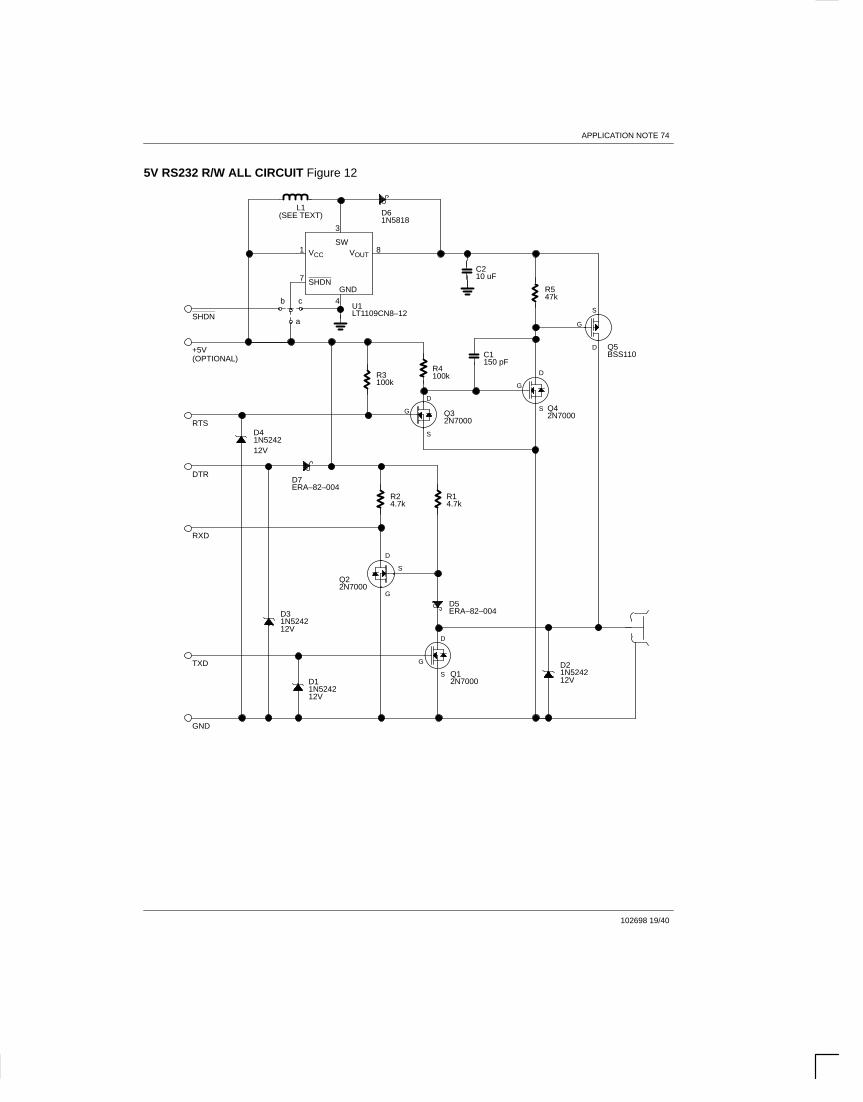
D. 5V RS232 R/W All (Voltage Converter)The universal upgrade of the interface of Figure 10 isshown in Figure 12. The components Q1, R1, D1, D2,Q2, R2, D3 and their functions are the same as before.Additional requirements include the control signal RTSwith the diode D4 for ESD protection, the diodes D5, D7,the cascaded inverters R3, Q3, R4 and Q4 & R5, C2, thepull–up switch Q5 and the controlled voltage converterIC1 with its external components L1, D6 and C2.
RTS is used to activate the pull–up switch Q5. DTR mayact as power supply, if it is able to source 5V at 25 mA.The strong pull–up is made possible by L1 and D6 if thevoltage converter is shut down. If idle (i.e., the bit con-trolling RTS in the Modem Control Register of the UARTis set to 1), RTS will be at 5V. To activate the pull–upswitch, the RTS bit in the UART (see Figure 8) must becleared to 0. This will cause a 0V level at the RTS pin ofthe RS232 connector. The DTR bit in the Modem Con-trol Register of the UART must be set to 1. If power issupplied from the outside, the status of DTR becomes adon’t care. In this case, D7 prevents driving the DTR linewith the external power supply.
For reliable operation of this circuit, DTR must reach ahigh level of 5V minimum. If this is not possible, an exter-nal 5V supply must be connected as shown in Figure 12.
The function of the other components of this circuit hasalready been explained in the section IV.C. RTS isequivalent to PGMEN in Figure 11. D5 now preventsfeedback from the 1–Wire bus to the internal power sup-ply during the programming pulse. The duration of theprogramming pulse (pulse width of RTS) cannot be con-trolled by the UART alone. Software to provide the cor-rect timing is found later in this document.
APPLICATION NOTE 74
102698 19/40
5V RS232 R/W ALL CIRCUIT Figure 12
D
G
S
D
G
S
D
G
S
D
G
S
S
D
G
3
4
81
7
SW
GNDSHDN
VCC VOUT
L1
U1LT1109CN8–12
D61N5818
C210 uF
R547k
R3100k
R4100k
C1150 pF
Q5BSS110
Q42N7000Q3
2N7000
Q12N7000
Q22N7000
R24.7k
R14.7k
D5ERA–82–004
D21N5242
D11N5242
D31N5242
D41N524212V
D7ERA–82–004
SHDN
+5V(OPTIONAL)
RTS
DTR
RXD
TXD
GND
(SEE TEXT)
12V
12V
12V
b c
a

DS9092TOUCHPROBE
DTR
GND
RXD
TXD
APPLICATION NOTE 74
102698 20/40
V. CIRCUITS FOR 12V RS232 INTERFACES(COM PORT)A. Read AllIf equipment has a true RS232 port using current limiteddrivers with voltage capabilities of at least ±8V, then asimple passive circuit is sufficient to interface to the1–Wire bus. Figure 13 shows all details; the waveformsare found on Figure 13a. This interface operates on thesame software as the circuit shown in Figure 10. Thewaveforms at RXD and TXD with respect to the comput-er’s ground are basically the same. The major differ-ence is that instead of 0V, a true negative voltage will befound, representing the idle state or a logic 1. Neglectingabsolute voltage levels, the waveform observed at RXDis essentially an inversion of the waveform that would beobserved on a 1–Wire data line for a 0V to 5V system.
The ground potential of the computer is different fromthe 1–Wire ground. This allows the iButton to experi-ence typical voltage levels (0V to 6V) on the 1–Wire dataline relative to the 1–Wire ground, while the serial portgenerates both positive and negative voltages relativeto the serial port ground. D1 clamps the data line to aconstant potential of nominally 3.9V. The time slots for1–Wire communication are generated by changing thepotential of the 1–Wire ground with respect to the1–Wire data line. The 1–Wire pullup resistor is in thepath from the 1–Wire ground to TXD, which provides thevoltage for the 1–Wire bus. D2 limits the voltage swingon the 1–Wire bus to a maximum value of 6.2 Volts.Since DTR is kept at 3.9V, D2 also limits the most nega-tive voltage occurring at RXD to –2.3V. D2 is conductingonly when the voltage at TXD is negative with respect tothe computer’s ground. D3 limits the voltage between1–Wire ground and 1–Wire data when the voltage atTXD is positive. D4 couples TXD with RXD when TXD ispositive and bypasses R1 to provide a low resistancepath to initiate a time slot on the 1–Wire bus. D4 is non-conducting when the voltage at TXD is negative withrespect to the computer’s ground. If an iButton pulls the1–Wire data line low (e. g. at a presence pulse or whensending out a zero data bit), it shorts DTR to RXD,resulting in a positive voltage at RXD. This positive volt-
age arrives as a zero in the UART’s receive data regis-ter.
Probing the 1–Wire bus at the data contact and the1–Wire ground with an oscilloscope, would show noth-ing unusual, except that the voltage swing is at theupper end of the tolerable range. Probing RXD and TXDwith another oscilloscope hooked up at the computer’sground, would also reveal quite normal waveforms. Theonly thing one might be concerned about is the poor neg-ative voltage of about –2.3V found at RXD. Probing allthree signals (1–Wire bus, TXD, RXD) with one oscillo-cope hooked up at the computer’s ground, would show anearly constant voltage of 3.9V at the 1–Wire bus.
The positive voltage of approximately +4.1V at RXD iswell within the RS232–specification, the negative volt-age is slightly out of specification. Since the total swingon the 1–Wire bus is limited to approximately 6V by thecharacteristics of iButtons, a more negative voltagecould be produced by replacing D1 by a zener diode of3.2V, for example. Unfortunately, this would increasethe permanent current load for DTR.
Fortunately, real RS232 receivers are more sensitive to aweak positive voltage than they are to a poor negativevoltage. Although it is not completely within the specifica-tion of RS232, this interface with the components speci-fied on Figure 13 has proven to be reliable with most desk-top personal computers. Small computers, especiallybattery powered models, might not have the required cur-rent capability to run this interface. In case of difficulties,one should use the 5V RS232 interface instead.
This interface is sold as COM Port Adapter DS9097. It isapplicable for reading all iButtons and writing to SRAM–based devices. Due to the high pullup voltage and thelow pullup resistor, this interface together with the rightsoftware also allows operation of the TemperatureiButton directly through the COM Port. Software to oper-ate this interface is explained later in this document.
12V RS232 READ ALL CIRCUIT Figure 13

TX
D
DT
R
RX
D
PC
–GN
D
ST
12
34
56
78
Sto
p
ST
12
34
56
12‘
34
56
Sto
pS
top
Sta
rt1
23
45
6S
top
Sta
rt1
23
45
6S
top
Sta
rt
=1–
WIR
EG
RO
UN
D
3.9V
TO
PC
–GR
OU
ND
0V A
S R
EF
ER
EN
CE
4.1V
3.9V
4.1V
4.1V
4.1V
3.9V
4.1V
–2.3
V–2
.3V
–2.3
V–2
.3V
–2.3
V–2
.3V
00
00
11
11
00
00
00
11
11
11
11
11
11
11
11
11
4.3V
4.3V
4.3V
4.3V
4.3V
–12V
–12V
–12V
–12V
–12V
SE
ND
F0
HE
X10
473
BP
S8
DA
TA B
ITS
NO
PA
RIT
Y, 1
ST
OP
BIT
SE
ND
00
HE
X(
6 B
ITS
)S
EN
D 3
F H
EX
SE
ND
3F
HE
XS
EN
D 3
F H
EX
1152
00 B
PS
6 D
ATA
BIT
SN
O P
AR
ITY,
1 S
TO
P B
IT
MA
TE
R W
RIT
E “
0” S
LOT
MA
ST
ER
WR
ITE
“1”
SLO
TM
AS
TE
R R
EA
D “
0” S
LOT
MA
ST
ER
RE
AD
“1”
SLO
T
MA
ST
ER
TX
MA
ST
ER
RX
GN
D
VC
C1–
WIR
E
“RE
SE
T P
ULS
E”
“PR
ES
EN
CE
PU
LSE
”
BU
S
480
us
480
us
60 u
s60
us
<15
us
15 u
s15
us
APPLICATION NOTE 74
102698 21/40
12V RS232 READ ALL WAVEFORMS Figure 13a
APPLICATION NOTE 74
102698 22/40
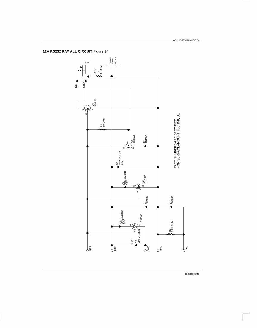
B. R/W AllThe simple adapter of Figure 13 can be upgraded forprogramming Add–Only Memories. Figure 14 showsthe details. R1 and the diodes D1 to D4 are the same inboth circuits. There is a new signal in use, called RTS.When doing normal 1–Wire communication, RTS isconstantly at a high positive voltage of nominally +12V.As long as the voltage at RTS remains positive, Q1 andQ2 are conducting. This allows D1 and D2 to provide thesame functions as in Figure 13. Since D1 and D2 areconducting, there is not enough voltage across D5 andD6 to draw any current. The gate–source voltage of Q3is determined by R2, R4, the voltage between DTR andRTS and the position of the contacts inside the connec-tor for the external DC supply. D7 prevents current flowfrom source to drain through the substrate diode of Q3when VDS is negative. If no external power supply isconnected, R2 and R4 form a voltage divider providing anegative VGS for Q3. With an external power supplyconnected, R2 will hold the gate of Q3 at the same levelas the source (VGS = 0V). None of these conditions willallow any current flow through Q3. With a positive volt-age at RTS, the p–channel transistor Q4 remains non–conducting, regardless if an external power supply isconnected or not. Thus the upgraded circuit behavesthe same as the simple COM–Port adapter.
To generate a programming pulse for EPROM baseddevices, RTS needs to be switched to a negative volt-age. This is done under software control by simply clear-ing the associated control bit in the UART and resettingthe bit as soon as the programming pulse needs to beended. Depending on whether an external supply isconnected or not, the behavior of this circuit is slightlydifferent.
If there is no external supply, Q4 has no function and thefollowing sequence occurs (Figure 14a): A negativevoltage at RTS will switch off Q1 and Q2, activating D5and D6 instead of D1 and D2. This increases the voltageat DTR from 3.9V to 6.8V and defines a limit of 12V forthe voltage on the 1–Wire bus. Simultaneously, the neg-ative voltage at RTS will make VGS of Q3 equal to thevoltage between DTR and RTS, which is a positivevalue. This will switch Q3 into a conducting state, feed-
ing the negative voltage from RTS through D7 to the1–Wire ground. As soon as the voltage on the 1–Wirebus reaches 12V, D6 will become active as voltage lim-iter. Thus the voltage on RTS is limited to approximately–5.4V. During the programming pulse, the voltage atRXD will be –5.2V instead of –2.3V. This has no impacton the logic of the UART, since a positive voltage isrequired to trigger the reception of a character.
The COM–Port powered mode of this circuit worksproperly if the RS232–drivers are able to provideenough current for programming. If more than one bit ofthe addressed memory byte need to be altered, thenmore current is needed during the programming pulse.Depending on the RS232 drivers, the available energymay not be sufficient for programming all bits of a byte.There are two possible solutions to this problem. Onepossibility uses an adaptive programming algorithm,where multiple passes are made for each byte. Forexample the software may program the first four bits ofevery byte on the first pass, and the remaining bits onthe second pass. The other possibility is to provide anauxiliary energy source, i.e., by connecting an external12V DC supply.
If the external supply is connected and operating, thecontacts inside the connector will open. This preventsany current flow through Q3. As the voltage at RTS goesnegative, Q1, Q2, D5, D6 will do the same as without theexternal supply. Instead of having no function, Q4 nowwill connect the negative end of the external voltagesource with the 1–Wire ground, providing the desiredlow–impedance programming voltage. Since RTS hasno other load than the gates of four transistors, there willbe the full voltage swing. The voltages at RXD and TXDare again determined by D5 and D6 and exhibit thesame waveforms as before.
This upgraded version of a COM–Port adapter isshipped with the iButton Starter Kit DS9092K and is alsoavailable as the DS9097E. It is applicable for readingand writing all iButtons. Due to the high pullup voltageand the low pullup resistor, this interface together withthe right software allows operation of the TemperatureiButton directly through the COM Port.
APPLICATION NOTE 74
102698 23/40
12V RS232 R/W ALL CIRCUIT Figure 14
RT
S
DT
R
GN
D
RX
D
TX
D
R1
1.5K
OH
M
D
G
S
D4
RB
400D
D
G
S
S
G
D
D S
G
D5
MM
BZ
5235
BQ
12N
7002
D1
MM
BZ
5228
B
6.8V
D3
RB
400D
D7
RB
400D
Q3
2N70
02
Q2
2N70
02
R2
1M O
HM
Q4
BS
S84
D6
MM
BZ
5242
BD
2M
MB
Z52
34B
R4
39 O
HM
DS
9092
PR
OB
E
NC
GN
D
3.9V
6.2V
12V
– +
+12
V•
PA
RT
NU
MB
ER
S A
RE
SP
EC
IFIE
DF
OR
SU
RFA
CE
–MO
UN
T T
EC
HN
IQU
E.
• • •
iBut
ton
APPLICATION NOTE 74
102698 24/40
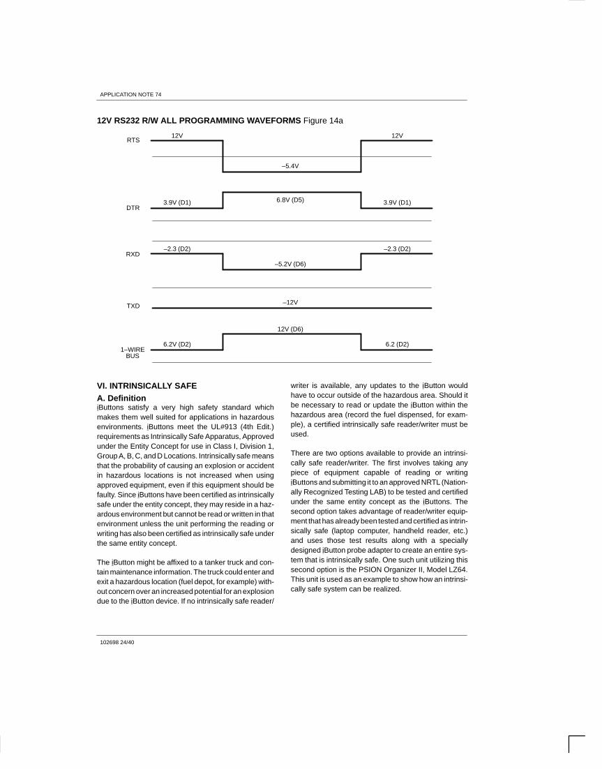
12V RS232 R/W ALL PROGRAMMING WAVEFORMS Figure 14a
–5.4V
6.8V (D5)
–5.2V (D6)
12V (D6)
12V 12V
3.9V (D1)
–2.3 (D2)
6.2 (D2)
3.9V (D1)
–2.3 (D2)
6.2V (D2)
–12V
RTS
DTR
RXD
TXD
1–WIREBUS
VI. INTRINSICALLY SAFEA. DefinitioniButtons satisfy a very high safety standard whichmakes them well suited for applications in hazardousenvironments. iButtons meet the UL#913 (4th Edit.)requirements as Intrinsically Safe Apparatus, Approvedunder the Entity Concept for use in Class I, Division 1,Group A, B, C, and D Locations. Intrinsically safe meansthat the probability of causing an explosion or accidentin hazardous locations is not increased when usingapproved equipment, even if this equipment should befaulty. Since iButtons have been certified as intrinsicallysafe under the entity concept, they may reside in a haz-ardous environment but cannot be read or written in thatenvironment unless the unit performing the reading orwriting has also been certified as intrinsically safe underthe same entity concept.
The iButton might be affixed to a tanker truck and con-tain maintenance information. The truck could enter andexit a hazardous location (fuel depot, for example) with-out concern over an increased potential for an explosiondue to the iButton device. If no intrinsically safe reader/
writer is available, any updates to the iButton wouldhave to occur outside of the hazardous area. Should itbe necessary to read or update the iButton within thehazardous area (record the fuel dispensed, for exam-ple), a certified intrinsically safe reader/writer must beused.
There are two options available to provide an intrinsi-cally safe reader/writer. The first involves taking anypiece of equipment capable of reading or writingiButtons and submitting it to an approved NRTL (Nation-ally Recognized Testing LAB) to be tested and certifiedunder the same entity concept as the iButtons. Thesecond option takes advantage of reader/writer equip-ment that has already been tested and certified as intrin-sically safe (laptop computer, handheld reader, etc.)and uses those test results along with a speciallydesigned iButton probe adapter to create an entire sys-tem that is intrinsically safe. One such unit utilizing thissecond option is the PSION Organizer II, Model LZ64.This unit is used as an example to show how an intrinsi-cally safe system can be realized.

APPLICATION NOTE 74
102698 25/40
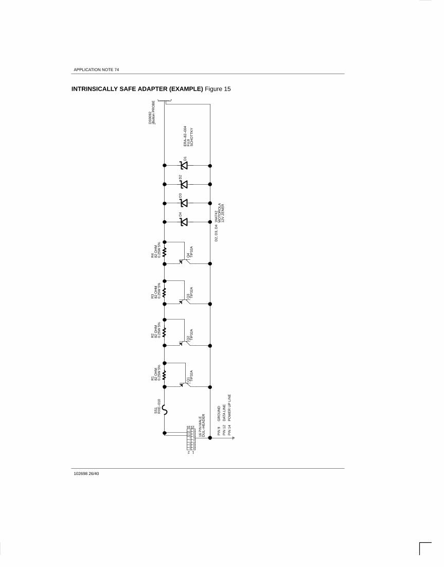
B. Example of an Intrinsically Safe SystemTo use the LZ64 as an intrinsically safe iButton Reader/Writer, an adapter is required. This adapter limits volt-ages and currents to safe values in the event a faultoccurs. In the case of a fault, due to its internal construc-tion, a maximum voltage of 17.22V at the 16–pin con-nector of the LZ64 may occur allowing a current of up to1.55A. The adapter discussed here limits these valuesat the iButton Probe to a maximum voltage of 15V and amaximum current of 10mA (Values required by theiButtons in order to be certified as intrinsically safe).These values together with the maximum inductance of18 µH and maximum capacitance of 0.2nF of an iButtonfulfill the requirements for a complete system that isintrinsically safe according to UL specifications.
Figure 15 shows the complete circuit of the adapter.Essential components are the four current shuntsQ1/R1 to Q4/R4, three Zener diodes D2 to D4 and oneself–resetting fuse SS1. The Schottky diode D1 isoptional. It protects iButtons by suppressing negativeundershoots on the 1–Wire bus.
If by fault the LZ64 presents up to 17.22V at its connec-tor and there is an open circuit at the iButton Probe, thenthe 12V Zener diodes D2 to D4 will limit the voltage atthe iButton Probe to a value well below 15V. The intrinsi-cally–safe regulations demand that this limitation willwork correctly even if two of the protecting devicesshould fail. Therefore three Zener diodes are providedinstead of one. If a Zener diode fails, it will either repre-sent a short or it will be non–conducting. In either case,the voltage at the iButton Probe is limited to a safe value.
If by fault the LZ64 presents up to 17.22V at its connec-tor and there is a short at the iButton Probe, then a cur-rent will flow through the resistors R1 to R4. The voltagedrop across these resistors acts to turn on their respec-tive transistors and causes base currents to flow. Thesebase currents multiplied by the current gain of the tran-sistors will direct most of the current to ground and limitthe current at the iButton Probe to less than 10mA. Q1will sink most of the current. Two of these Q/R stagesare required to limit the current available at the iButtonProbe under worst case conditions to less than 10 mA.The other two current shunts are redundant since againthe circuit must operate correctly with up to two faults.
The self–resetting fuse with a trip point below 100mAwill open in less than one second and thus prevent ther-mal damage to the transistors. It will also serve as anindicator to the operator that a fault or malfunction hasoccurred.
Although this adapter is designed for use with the LZ64,it can be used with similar intrinsically safe equipmentwith the same or lower faulted open–circuit voltage orshort–circuit current to form an iButton Reader/Writer.This adapter does not impede writing to EPROM basediButtons.
VII. COMMENTED SOFTWAREA. Software Architectural ModelThe software that manages data transfer to and fromiButtons is related to the ISO reference model of OpenSystem Interconnection (OSI). This model specifies alayered protocol having up to seven layers, denoted asPhysical, Link, Network, Transport, Session, Presenta-tion, and Application. The Application layer representsthe final application designed by the customer. A Ses-sion layer may or may not be needed, depending on theenvironment in which the iButtons are used.
According to the ISO model, the electrical and timingrequirements of iButton and the characteristics of the1–Wire bus comprise the Physical layer. Details havealready been given in section II of this document.
The Link layer defines the basic communication func-tions of iButtons, which are the hardware dependentfunctions of Reset, Presence Detect and bit transfer.Circuits for interfacing iButtons and general informationon the software to operate these interfaces havealready been presented in sections III, IV, and V. In thissection, the software itself, specifically the functionsTouchReset and TouchByte, are discussed in detail.
The Network layer provides the identification of iButtonsand the associated network capabilities based on theunique lasered identification number. Software for thislayer is built up using the low–level functions of the LinkLayer. Since this software is independent of any particu-lar interface, it is not within the scope of this document.
APPLICATION NOTE 74
102698 26/40
INTRINSICALLY SAFE ADAPTER (EXAMPLE) Figure 15
12
1516
16 P
IN M
ALE
DU
L–H
EA
DE
R
Q1
Q2
Q3
Q4
D4
D3
D2
DS
9092
iBut
ton
PR
OB
E
D1
ER
A–8
2–00
4F
UJI
SC
HO
TT
KY
PIN
9G
RO
UN
D
PIN
12
PIN
14
DA
TA L
INE
PO
WE
R U
P L
INE
D2,
D3,
D4
1N47
42M
OTO
RO
LA12
V Z
EN
ER
SS
1R
XE
–010
R2
82 O
HM
0.25
W 5
%
R1
82 O
HM
0.25
W 5
%
R3
82 O
HM
0.25
W 5
%
R4
82 O
HM
0.25
W 5
%
TIP
32A
TIP
32A
TIP
32A
TIP
32A
APPLICATION NOTE 74
102698 27/40
The Transport layer is responsible for the data transferbetween the non–ROM segments of iButtons and themaster, and the data transfer from the scratchpad to thefinal storage areas and special registers of the iButton.Due to their EPROM technology, Add–Only Memoriesrequire special attention for writing data. The Tempera-ture iButton may require special hardware together withappropriate software to do a temperature measure-ment. To comply these devices, the hardware specificfunction PulWidth has been provided on the Transportlayer. Details are given in this chapter. All other softwareof the transport layer is independent of the type of inter-face, and therefore is not discussed here.
The layers Link, Network, and Transport are the founda-tions of the Presentation layer. This layer provides aDOS–like file system supporting functions like Format,Directory, Type, Copy, Delete, Optimize, and integritycheck. Since the Presentation layer itself is based onsoftware of the lower layers, its software is independentof any particular interface. Full details of the Presenta-tion layer are given in the iButton TMEX Professional
Software Developer’s Kit DS0621–SDK. For softwareexamples beyond the hardware dependent functionsTouchReset, TouchByte and PulWidth, please refer tothe “Book of DS19xx iButton Standards” and the iButtonStarter Kit DS9092K.
A matrix that indicates which software of this sectionmatches with which hardware is given in Table 3. For the5V TTL type interface, assembly language code for the8051 has been provided. For the group of interfacesbased on the UART 8250, code examples in Pascal andC are included. This particular software has beenadapted to and verified with IBM–compatible PCsemploying a 8253 timer at 2.3863633 MHz and runningunder DOS. The timing is practically independent of theCPU clock rate. Under WINDOWS there is a lot moresoftware being executed around an application pro-gram. This overhead introduces a significant influencefrom the CPU clock rate to the desired timing with thefunction PulWidth. The functions TouchReset andTouchByte are timed by the UART only and thereforeare independent of the operating system.
SOFTWARE/HARDWARE MATRIX Table 3
LANGUAGE 8051 ASM PASCAL AND C
TIMING CPU CRYSTAL 8250 UART (1.8 MHz) and 8253 TIMER (2.4 MHz)
Electric Type 5V TTL 5V RS232, 12V RS232
SRAM R/WEPROM Read
TouchReset, TouchByte 1.8 or 11 MHz TouchReset and TouchByte Pascal or C–Lan-guage
EPROM Write 0.5 ms pulsewidth:PULWIDTH(1) at 1.8 MHzPULWIDTH(6) at 11 MHz
0.5 ms pulsewidth:PULWIDTH(1193)under DOS
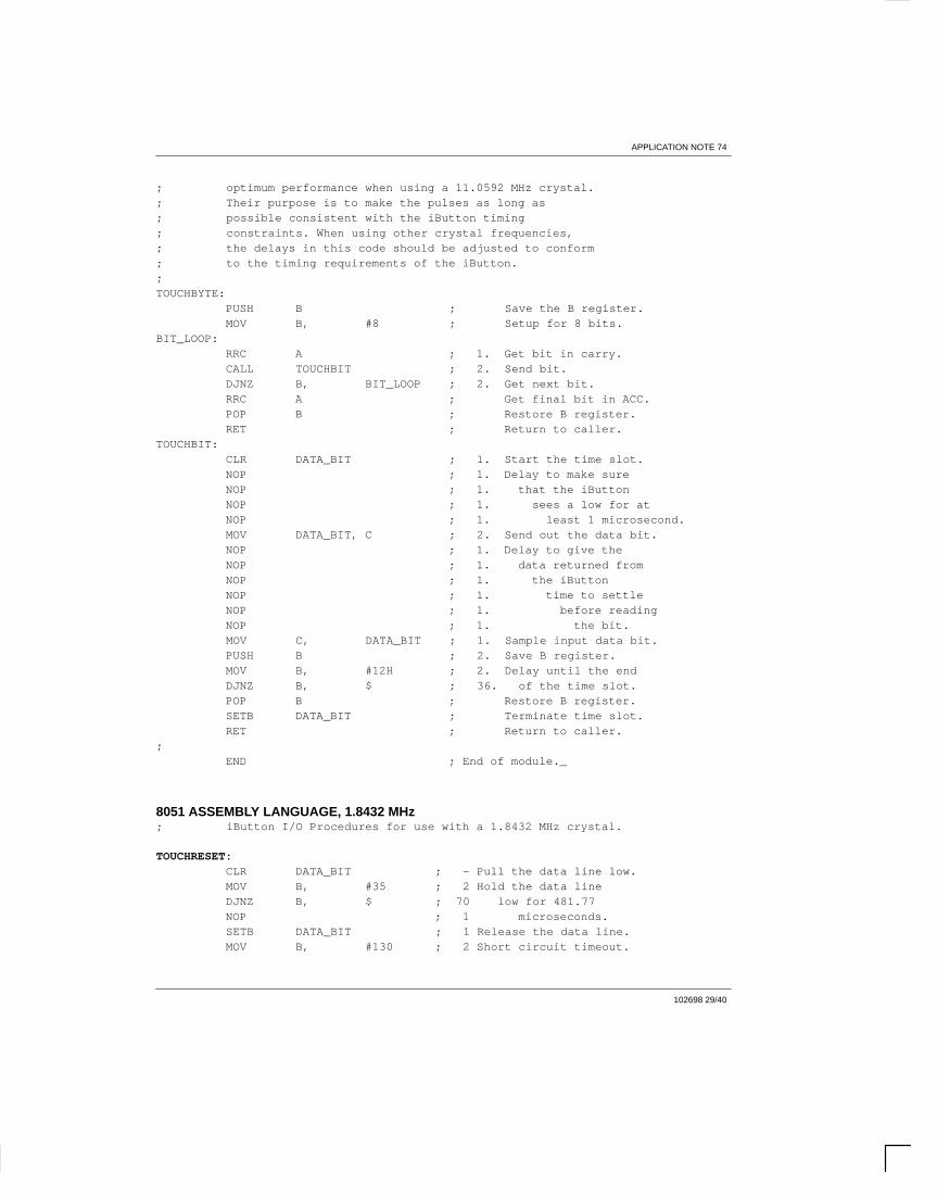
B. TTL–Interface R/W AllAs a representative for all microprocessor timed 1–Wireinterfaces the industry–standard 8051 microcontrollerhas been chosen. The following pages show two ver-sions of assembly language code to provide the func-tions TouchReset and TouchByte. The first example iswritten for an 11.0592 MHz crystal, the second one for1.8432 MHz. The higher frequency is very commonsince it supports all standard baud rates with the highestaccuracy. The lower frequency is the lowest that cancomply with the 1–Wire timing. The port to be used as1–Wire bus is defined in the parameter DATA_BIT.Parameter passing from the subroutines TouchResetand TouchByte is very simple: If an iButton is present on
the 1–Wire bus, TouchReset will return a set carry flag;otherwise carry is cleared. To send one byte to the1–Wire bus, the byte to be sent is loaded into the accu-mulator before calling TouchByte. If one intends to read,the accumulator is loaded with FFH. This generates cor-rect Read Data Time Slots and returns data from the1–Wire bus to the calling program through the accumu-lator. These conventions are valid for both versions ofTouchReset and TouchByte.
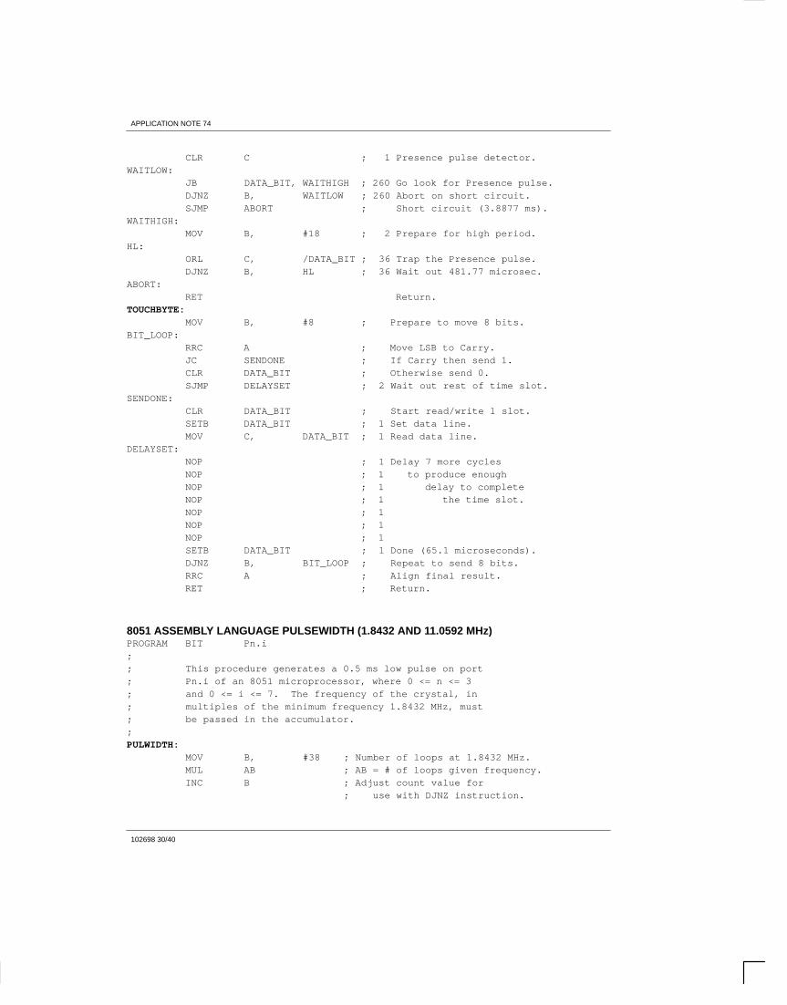
The procedure to generate a programming pulse is thesame for both clock frequencies. It generates a 0.5 msLOW pulse at the port named PROGRAM. If the clockfrequency is 1.8 MHz, then the accumulator needs to be
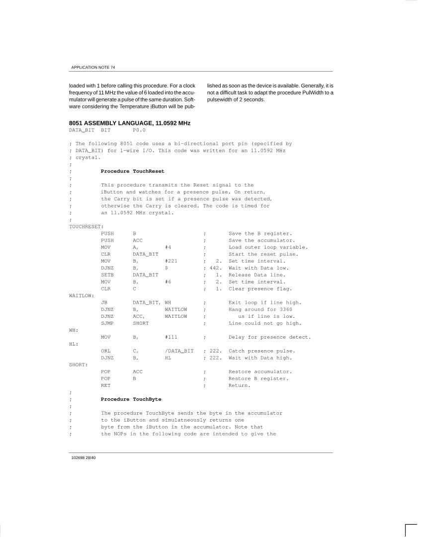
APPLICATION NOTE 74
102698 28/40
loaded with 1 before calling this procedure. For a clockfrequency of 11 MHz the value of 6 loaded into the accu-mulator will generate a pulse of the same duration. Soft-ware considering the Temperature iButton will be pub-
lished as soon as the device is available. Generally, it isnot a difficult task to adapt the procedure PulWidth to apulsewidth of 2 seconds.
8051 ASSEMBLY LANGUAGE, 11.0592 MHzDATA_BIT BIT P0.0
; The following 8051 code uses a bi–directional port pin (specified by; DATA_BIT) for 1–wire I/O. This code was written for an 11.0592 MHz; crystal.;; Procedure TouchReset;; This procedure transmits the Reset signal to the ; iButton and watches for a presence pulse. On return,; the Carry bit is set if a presence pulse was detected,; otherwise the Carry is cleared. The code is timed for; an 11.0592 MHz crystal.;TOUCHRESET: PUSH B ; Save the B register. PUSH ACC ; Save the accumulator. MOV A, #4 ; Load outer loop variable. CLR DATA_BIT ; Start the reset pulse. MOV B, #221 ; 2. Set time interval. DJNZ B, $ ; 442. Wait with Data low. SETB DATA_BIT ; 1. Release Data line. MOV B, #6 ; 2. Set time interval. CLR C ; 1. Clear presence flag.WAITLOW: JB DATA_BIT, WH ; Exit loop if line high. DJNZ B, WAITLOW ; Hang around for 3360 DJNZ ACC, WAITLOW ; us if line is low. SJMP SHORT ; Line could not go high.WH: MOV B, #111 ; Delay for presence detect.HL: ORL C, /DATA_BIT ; 222. Catch presence pulse. DJNZ B, HL ; 222. Wait with Data high.SHORT: POP ACC ; Restore accumulator. POP B ; Restore B register. RET ; Return.;; Procedure TouchByte;; The procedure TouchByte sends the byte in the accumulator; to the iButton and simulatneously returns one ; byte from the iButton in the accumulator. Note that; the NOPs in the following code are intended to give the
APPLICATION NOTE 74
102698 29/40
; optimum performance when using a 11.0592 MHz crystal.; Their purpose is to make the pulses as long as; possible consistent with the iButton timing; constraints. When using other crystal frequencies,; the delays in this code should be adjusted to conform; to the timing requirements of the iButton.;TOUCHBYTE: PUSH B ; Save the B register. MOV B, #8 ; Setup for 8 bits.BIT_LOOP: RRC A ; 1. Get bit in carry. CALL TOUCHBIT ; 2. Send bit. DJNZ B, BIT_LOOP ; 2. Get next bit. RRC A ; Get final bit in ACC. POP B ; Restore B register. RET ; Return to caller.TOUCHBIT: CLR DATA_BIT ; 1. Start the time slot. NOP ; 1. Delay to make sure NOP ; 1. that the iButton NOP ; 1. sees a low for at NOP ; 1. least 1 microsecond. MOV DATA_BIT, C ; 2. Send out the data bit. NOP ; 1. Delay to give the NOP ; 1. data returned from NOP ; 1. the iButton NOP ; 1. time to settle NOP ; 1. before reading NOP ; 1. the bit. MOV C, DATA_BIT ; 1. Sample input data bit. PUSH B ; 2. Save B register. MOV B, #12H ; 2. Delay until the end DJNZ B, $ ; 36. of the time slot. POP B ; Restore B register. SETB DATA_BIT ; Terminate time slot. RET ; Return to caller.; END ; End of module._
8051 ASSEMBLY LANGUAGE, 1.8432 MHz; iButton I/O Procedures for use with a 1.8432 MHz crystal.
TOUCHRESET: CLR DATA_BIT ; – Pull the data line low. MOV B, #35 ; 2 Hold the data line DJNZ B, $ ; 70 low for 481.77 NOP ; 1 microseconds. SETB DATA_BIT ; 1 Release the data line. MOV B, #130 ; 2 Short circuit timeout.
APPLICATION NOTE 74
102698 30/40
CLR C ; 1 Presence pulse detector.WAITLOW: JB DATA_BIT, WAITHIGH ; 260 Go look for Presence pulse. DJNZ B, WAITLOW ; 260 Abort on short circuit. SJMP ABORT ; Short circuit (3.8877 ms).WAITHIGH: MOV B, #18 ; 2 Prepare for high period.HL: ORL C, /DATA_BIT ; 36 Trap the Presence pulse. DJNZ B, HL ; 36 Wait out 481.77 microsec.ABORT: RET Return.TOUCHBYTE: MOV B, #8 ; Prepare to move 8 bits.BIT_LOOP: RRC A ; Move LSB to Carry. JC SENDONE ; If Carry then send 1. CLR DATA_BIT ; Otherwise send 0. SJMP DELAYSET ; 2 Wait out rest of time slot.SENDONE: CLR DATA_BIT ; Start read/write 1 slot. SETB DATA_BIT ; 1 Set data line. MOV C, DATA_BIT ; 1 Read data line.DELAYSET: NOP ; 1 Delay 7 more cycles NOP ; 1 to produce enough NOP ; 1 delay to complete NOP ; 1 the time slot. NOP ; 1 NOP ; 1 NOP ; 1 SETB DATA_BIT ; 1 Done (65.1 microseconds). DJNZ B, BIT_LOOP ; Repeat to send 8 bits. RRC A ; Align final result. RET ; Return.
8051 ASSEMBLY LANGUAGE PULSEWIDTH (1.8432 AND 11.0592 MHz)PROGRAM BIT Pn.i;; This procedure generates a 0.5 ms low pulse on port; Pn.i of an 8051 microprocessor, where 0 <= n <= 3; and 0 <= i <= 7. The frequency of the crystal, in; multiples of the minimum frequency 1.8432 MHz, must; be passed in the accumulator.;PULWIDTH: MOV B, #38 ; Number of loops at 1.8432 MHz. MUL AB ; AB = # of loops given frequency. INC B ; Adjust count value for ; use with DJNZ instruction.
APPLICATION NOTE 74
102698 31/40
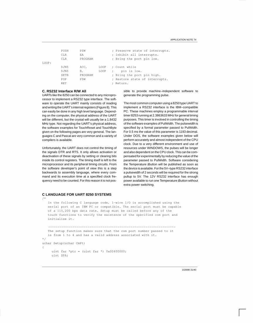
PUSH PSW ; Preserve state of interrupts. CLR EA ; Inhibit all interrupts. CLR PROGRAM ; Bring the port pin low.LOOP: DJNZ ACC, LOOP ; Count while DJNZ B, LOOP ; pin is low. SETB PROGRAM ; Bring the port pin high. POP PSW ; Restore state of interrupts. RET ; Return.
C. RS232 Interface R/W AllUARTs like the 8250 can be connected to any micropro-cessor to implement a RS232 type interface. The soft-ware to operate the UART mainly consists of readingand writing the UART’s internal registers (Figure 8). Thiscan easily be done in any high level language. Depend-ing on the computer, the physical address of the UARTwill be different, but the crystal will usually be a 1.8432MHz type. Not regarding the UART’s physical address,the software examples for TouchReset and TouchBytegiven on the following pages are very general. The lan-guages C and Pascal are very common and a variety ofcompilers is available.
Unfortunately, the UART does not control the timing ofthe signals DTR and RTS. It only allows activation ordeactivation of these signals by setting or clearing bitsinside its control registers. The timing itself is left to themicroprocessor and its peripheral timing circuits. Fromthe software developer’s point of view this is a stepbackwards to assembly language, where every com-mand and its execution time at a specified clock fre-quency need to be counted. For this reason it is not pos-
sible to provide machine–independent software togenerate the programming pulse.
The most common computer using a 8250 type UART toimplement a RS232 interface is the IBM–compatiblePC. These machines employ a programmable intervaltimer 8253 running at 2.3863633 MHz for general timingpurposes. This timer is involved in controlling the timingof the software examples of PulWidth. The pulsewidth isspecified by a formal parameter passed to PulWidth.For 0.5 ms the value of this parameter is 1193 decimal.Under DOS, the software examples given below willperform accurately and almost independent of the CPUclock. Due to a very different environment and use ofresources under WINDOWS, the pulses will be longerand also dependent on the CPU clock. This can be com-pensated for experimentally by reducing the value of theparameter passed to PulWidth. Software consideringthe Temperature iButton will be published as soon asthe device is available. For the 5V–type RS232 interfacea pulsewidth of 2 seconds will be required for the strongpullup to 5V. The 12V RS232 interface has enoughpower available to run one Temperature iButton withoutextra power switching.
C LANGUAGE FOR UART 8250 SYSTEMS/* In the following C language code, 1–wire I/O is accomplished using the serial port of an IBM PC or compatible. The serial port must be capable of a 115,200 bps data rate. Setup must be called before any of the touch functions to verify the existence of the specified com port and initialize it.
–––––––––––––––––––––––––––––––––––––––––––––––––––––––––––––––––––– The setup function makes sure that the com port number passed to it is from 1 to 4 and has a valid address associated with it.*/uchar Setup(uchar CmPt) uint far *ptr = (uint far *) 0x00400000; uint SPA;
APPLICATION NOTE 74
102698 32/40
/* check to see if it is a valid com port number and address */ SPA = *(ptr+CmPt–1); /* get the address */ if (CmPt < 1 || CmPt > 4 || !SPA ) return FL;
/* serial port initialization */ outportb(SPA+3,0x83); /* set DLAB */ outportb(SPA ,0x01); /* bit rate is 115200 */ outportb(SPA+1,0x00); outportb(SPA+3,0x03); /* 8 dta, 1 stp, no par */ outportb(SPA+1,0x00); /* no interrupts */ outportb(SPA+4,0x03); /* RTS and DTR on */
return TR;
/*–––––––––––––––––––––––––––––––––––––––––––––––––––––––––––––––––––––––– * Do a reset on the 1 wire port and return 0 no presence detect * 1 presence pulse no alarm * 2 alarm followed by presence * 3 short circuit to ground * 4 no com port found * * The global variable ’com_port’ must be set to the com port that the * DS9097 COM Port Adapter is attached to before calling this routine. * */uchar TouchReset( void ) uint SPA,F,X,Y,tmp,trst=0; uint far *ptr = (uint far *) 0x00400000; ulong far *sysclk = (ulong far *) 0x0040006c; ulong M;
/* get the serial port address */ SPA = *(ptr+com_port–1);
/* return if there is no address */ if (!SPA) return 4;
/* serial port initialization */ outportb(SPA+3,0x83); /* set DLAB */ outportb(SPA ,0x01); /* bit rate is 115200 */ outportb(SPA+1,0x00); outportb(SPA+3,0x03); /* 8 dta, 1 stp, no par */ outportb(SPA+1,0x00); /* no interrupts */ outportb(SPA+4,0x03); /* RTS and DTR on */
/* Initialize the time limit */ M = *sysclk +1;
APPLICATION NOTE 74
102698 33/40
/* loop to clear the buffers */ do tmp = inportb(SPA+5) & 0x60; while (tmp != 0x60);
/* flush input */ while (inportb(SPA+5) & 0x1) X = inportb(SPA);
outportb(SPA+3,0x83); /* set DLAB */ outportb(SPA+1,0x00); /* baud rate is 10473 */ outportb(SPA ,0x0B); outportb(SPA+3,0x03); /* 8 dta, 1 stp, no par */ outportb(SPA ,0xF0); /* send the reset pulse */
/* wait until character back or timeout */ do Y = inportb(SPA+5); F = Y & 0x1; while ( !F && (*sysclk <= M) );
if (F) X = inportb(SPA); else return 3;
if (X != 0xF0) /* if more bits back than sent then there */ /* is a device if framing error or break */ trst = TR; if ( (Y & 0x18) != 0 ) trst = 2;
/* loop to clear the buffers */ do tmp = inportb(SPA+5) & 0x60; while (tmp != 0x60);
/* wait until character back or timeout */ do Y = inportb(SPA+5); F = Y & 0x1; while ( !F && (*sysclk <= M) );
if (F) X = inportb(SPA); else return 3;
outportb(SPA+3,0x83); /* set DLAB */ outportb(SPA ,0x01); /* bit rate is 115200 */ outportb(SPA+3,0x03); /* 8 dta, 1 stp, no par */
return trst;

APPLICATION NOTE 74
102698 34/40
/*–––––––––––––––––––––––––––––––––––––––––––––––––––––––––––––––––––––––– * This is the 1–Wire routine ’TouchByte’, sometimes called ’DataByte’. * It transmits 8 bits onto the 1–Wire data line and receives 8 bits * concurrently. The global variable ’com_port’ must be set to the * com port that the serial brick is attached to before calling this * routine. This com port must also be set to 115200 baud, 8 dta, 1 stp, * and no parity. This routine returns the uchar 8 bit value received. * If it times out waiting for a character then 0xFF is returned. */uchar TouchByte(uchar outch) uchar inch=0,sendbit,Mask=1; uint SPA; uint far *ptr = (uint far *) 0x00400000; ulong far *sysclk = (ulong far *) 0x0040006c; ulong M;
/* get the serial port address */ SPA = *(ptr+com_port–1);
/* Initialize the time limit */ M = *sysclk +2;
/* wait to TBE and TSRE */ do while ( (inportb(SPA+5) & 0x60) != 0x60 );
/* flush input */ while ( (inportb(SPA+5) & 0x1) ) inportb(SPA);
/* get first bit ready to go out */ sendbit = (outch & 0x1) ? 0xFF : 0x00;
/* loop to send and receive 8 bits */ do outportb(SPA,sendbit); /* send out the bit */
/* get next bit ready to go out */ Mask <<= 1; sendbit = (outch & Mask) ? 0xFF : 0x00;
/* shift input char over ready for next bit */ inch >>= 1;
/* loop to look for the incoming bit */ for (;;) /* return if out of time */ if ( *sysclk > M ) return 0xFF;

APPLICATION NOTE 74
102698 35/40
if ( inportb(SPA+5) & 0x01 ) inch |= ((inportb(SPA) & 0x01) ? 0x80 : 0x00); break;
while (Mask);
return inch; /* return the input char */
C LANGUAGE PULSEWIDTH FOR SYSTEMS USING 8253 AND 8250// standard include header file#include <dos.h>
// function prototypevoid PulWidth(unsigned int);
// global variableint SPA;
//–––––––––––––––––––––––––––––––––––––––––––––––––––––––––––––––––––––––––// This procedure creates a fixed pulse width for programming that is// approximately independent of system clock speed. X is in units of// 0.419 microseconds for values greater than about 1000.//void PulWidth(unsigned int X) unsigned int N,M;
disable(); // turn off interrupts outportb(SPA+4,(inportb(SPA+4) & 0xFD)); // apply program pulse to rts outportb(0x43,0); // freeze value in timer M = inportb(0x40); // read value in timer M |= (inportb(0x40) << 8); do outport(0x43,0); // freese value in timer N = inportb(0x40); // read value in timer N |= (inportb(0x40) << 8); while (X > (M – N));
outportb(SPA+4,(inportb(SPA+4) | 0x02)); // remove program Voltage enable(); // turn interrupts on
APPLICATION NOTE 74
102698 36/40
PASCAL LANGUAGE FOR UART 8250 SYSTEMS In the following pascal code 1–wire I/O is accomplished using the serial port of an IBM PC or compatible. The serial port must be capable of a 115,200 bps data rate.Const SPA : Word = 0; Currently active serial port address
Function TouchReset(N: Byte): Boolean; This function transmits the one–wire protocol reset sequence to the device connected to COM port number N. This sequence consists of a low pulse lasting a mimimum of 480 us followed by a high dead time lasting a mimimum of 480 us. The function returns True if a presence detect pulse occurs during the dead time, otherwise it returns False.Const Init : Array[1..4] of Boolean = (True, True, True, True);
Var S : Array[1..4] of Word Absolute $40:0; T : LongInt Absolute $40:$6C; M : LongInt; F : Boolean; X, Y : Byte;
Begin SPA := 0; TouchReset := False; Assume failure If (N > 0) and (N < 5) and (S[N] > 0) then Begin Legal port # SPA := S[N]; Save active serial port address If Init[N] then Begin Serial port requires initialization Port[SPA +3] := $83; Set the DLAB Port[SPA] := 1; Bit rate is Port[SPA +1] := 0; 115200 bps Port[SPA +3] := 3; 8 dta, 1 stp, no par Port[SPA +1] := 0; No interrupts Port[SPA +4] := 3; RTS and DTR on Init[N] := False; Initialization completed End; M := T +1; Initialize the time limit Repeat until Port[SPA +5] and $60 = $60; Await TBE & TSRE While Odd(Port[SPA +5]) do X := Port[SPA]; Flush input Port[SPA +3] := $83; Set DLAB port[SPA+1] := 0; Baud rate is 10473 Port[SPA] := 11; Port[SPA +3] := 3; 8 data, 1 stop, no parity Port[SPA] := $F0; Send the reset pulse Repeat Wait until character back or timeout Y := Port[SPA +5]; F := Odd(Y);

APPLICATION NOTE 74
102698 37/40
until F or (T > M); If F then X := Port[SPA] else X := $F0; If (X <> $F0) Then Begin If more bits back than sent TouchReset := True; then there is a device If ((Y and $18) <> 0) Then Begin Framing error or break Repeat until Port[SPA +5] and $60 = $60; TBE & TSRE Repeat F := Odd(Port[SPA +5]) until F or (T > M); If F then X := Port[SPA]; End; End; Port[SPA +3] := $83; Set the DLAB Port[SPA] := 1; Bit rate is 115200 bps Port[SPA +3] := 3; 8 dta, 1 stp, no par End;End;
Function TouchByte(X: Byte): Byte; This function transmits the byte X to the device attached to the currently active serial port SPA, and returns a byte from the device as its value.Var T : LongInt Absolute $40:$6C; M : LongInt; I, J : Byte;Begin If SPA = 0 then TouchByte := X else Begin M := T +1; Initialize the time limit Repeat until Port[SPA +5] and $60 = $60; Await TBE & TSRE While Odd(Port[SPA +5]) do I := Port[SPA]; Flush input I := 0; J := 0; Initialize output & input bit counters Repeat If Odd(Port[SPA +5]) then Begin Inc(J); If Odd(Port[SPA]) then X := X or $80; End else If (I<=J) and (Port[SPA+5] and $20 = $20) then Begin If Odd(X) then Port[SPA] := $FF else Port[SPA] := 0; X := X shr 1; Inc(I); End; Until (J = 8) or (T > M); While (J < 8) do Begin X := X shr 1 or $80; Inc(J) End; TouchByte := X; End;End;
APPLICATION NOTE 74
102698 38/40
PASCAL LANGUAGE PULSEWIDTH FOR SYSTEMS USING 8253 AND 8250Procedure PulWidth(X : Word); This procedure creates a fixed pulse width for programming that is approximately independent of system clock speed. When used in an IBM PC or compatible computer operating under MS– DOS, X is in units of 0.419 microseconds for values of X greater than about 1000. The procedure can be used with any processor having an 8250 UART I/O mapped to base port address SPA and an 8253 timer mapped to base port address $40, operating with an input clock of 2.386363 MHz and with its count limit set to the maximum value.Var M, N : Word;Begin Inline($FA); Turn off interrupts Port[SPA +4] := Port[SPA +4] and $FD; Apply Program Pulse on RTS Port[$43] := 0; Freeze value in timer M := Port[$40] shl 8 or Port[$40]; Read value in timer Repeat Loop to consume real time Port[$43] := 0; Freeze value in timer again N := Port[$40] shl 8 or Port[$40]; Read new value in timer Until M – N >= X; See if ”X” usec have elapsed Port[SPA +4] := Port[SPA +4] or 2; Remove Program Voltage Inline($FB); Turn interrupts onEnd;
VIII. SUMMARYThis application note explains the hardware of differenttypes of 1–Wire interfaces and software examplesadapted to this hardware. Depending on the types ofiButtons required for a project and the type of computerto be used, the most economic interface is easily found.The hardware examples shown are basically two differ-ent types: 5V general interface and 12V RS232 inter-face. Within the 5V group a common printed circuitboard could be used for all four circuits. The variationscan be achieved by different population of components(Table 4). The same principle is used for the 12V RS232interface. The population determines if it is a Read all ora Read/Write all type of interface (Table 5).
There are other possible circuit implementations tocreate a 1–Wire interface. The circuits described in thisapplication note cover many different configurations.For a custom application, one of the described optionscan be adapted to meet individual needs. The circuitscan be used for reading and writing SRAM basediButtons, for individually programming EPROM basediButtons and for temperature measurement with theDS1920 Temperature iButton. For programming largequantities of EPROM based iButtons with the same data(gang programming) commercial programmers areavailable from several independent companies. A list ofvendors is available from Dallas Semiconductor onrequest.
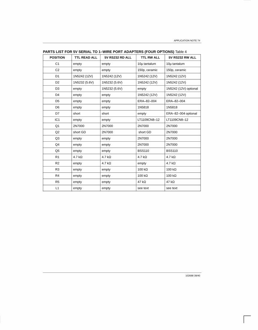
APPLICATION NOTE 74
102698 39/40
PARTS LIST FOR 5V SERIAL TO 1–WIRE PORT ADAPTERS (FOUR OPTIONS) Table 4
POSITION TTL READ ALL 5V RS232 RD ALL TTL RW ALL 5V RS232 RW ALL
C1 empty empty 10µ tantalum 10µ tantalum
C2 empty empty 150p, ceramic 150p, ceramic
D1 1N5242 (12V) 1N5242 (12V) 1N5242 (12V) 1N5242 (12V)
D2 1N5232 (5.6V) 1N5232 (5.6V) 1N5242 (12V) 1N5242 (12V)
D3 empty 1N5232 (5.6V) empty 1N5242 (12V) optional
D4 empty empty 1N5242 (12V) 1N5242 (12V)
D5 empty empty ERA–82–004 ERA–82–004
D6 empty empty 1N5818 1N5818
D7 short short empty ERA–82–004 optional
IC1 empty empty LT1109CN8–12 LT1109CN8–12
Q1 2N7000 2N7000 2N7000 2N7000
Q2 short GD 2N7000 short GD 2N7000
Q3 empty empty 2N7000 2N7000
Q4 empty empty 2N7000 2N7000
Q5 empty empty BSS110 BSS110
R1 4.7 kΩ 4.7 kΩ 4.7 kΩ 4.7 kΩ
R2 empty 4.7 kΩ empty 4.7 kΩ
R3 empty empty 100 kΩ 100 kΩ
R4 empty empty 100 kΩ 100 kΩ
R5 empty empty 47 kΩ 47 kΩ
L1 empty empty see text see text

APPLICATION NOTE 74
102698 40/40
PARTS LIST FOR 12V COM PORT TO 1–WIRE ADAPTERS (TWO OPTIONS) Table 5
POSITION READ ALL RW ALL
D1 empty 1N5228 (3.9V)
D2 empty 1N5234 (6.2V)
D3 ERA–82–004 ERA–82–004
D4 ERA–82–004 ERA–82–004
D5 1N5228 (3.9V) 1N5235 (6.8V)
D6 1N5234 (6.2V) 1N5242 (12V)
D7 empty ERA–82–004
Q1 empty 2N7000
Q2 empty 2N7000
Q3 empty 2N7000
Q4 empty BSS110
R1 1.5 kΩ 1.5 kΩ
R2 empty 1000 kΩ
R3 empty empty
R4 empty 39 Ω