atomic layer deposition of ferroelectric and threshold ... layer deposition of ferroelectric and...
TRANSCRIPT

Atomic Layer Deposition of Ferroelectric and Threshold Switching Materials for Next
Generation Nonvolatile MemoryKarl Littau, Stephen L. Weeks, Ashish Pal, Vijay Narasimhan, Greg Nowling, Michael Bowes,
Sergey V. Barabash, Dipankar Pramanik, and Tony Chiang

Who We Are:
Trusted Partner For Materials Innovation
World-class
interdisciplinary team
Serving large markets
where new materials are keyUnique high-throughput
experimentation platform
Top memory semiconductor
manufacturers are customers
State-of-the art development
facility and characterization
Fast
FactsFounded:
2004
Intermolecular:
HQ in San Jose, CA, USA
50,000 sq. ft. High Throughput Materials Experimentation Facility
IPO:
2011 (NASDAQ:IMI)
Unique high-throughput
experimentation platform
State-of-the art development
facility and characterizationWorld-class
interdisciplinary team
Serving large markets
where new materials are key

Materials Are at the Core of Innovation in the 21st Century
• Weight
• Space
• Flexibility
• Temperature
• Energy Efficiency
• Smart Buildings
• Lightweight
• Energy Efficiency
• Performance
• Power
• Cost
• Scaling
• Heat Management
• Lightweight
• Energy Efficiency

Risk management
of new materials
The Materials Innovation Problem
Many options, one
experiment at a time
Limited R&D infrastructure
for experimentation
Materials
innovation
is complex, costly
and slow
Long learning
cycle times
Empirical approach
needed
Manufacturing environment
is adverse to change

Discovery and Innovation Process
Mapping Materials Space
• Search application specific novel materials• Composition, mechanical, electrical, optical characterization
Deep Understanding of Options
• Characterization with application specific tests
• Develop and provide empirical models
Insertion into Manufacturing
• Application specific multi-layers
• Early process scale-up and validation
Results
Best candidates
for exploration
Best candidates
for applications
Manufacturing compatibility

2-ALD, 1-PVD
Integrated Cluster Platform with ALD and PVD
Platform Highlights
Intermolecular designed and built an advanced R&D
platform for thin film deposition, enabling rapid exploration
of complex materials
• Cluster platform to enable in-situ processing
• A-30 ALD (Atomic Layer Deposition) systems enable
full-wafer or quadrant-isolated depositions
• P-30 PVD (Physical Vapor Deposition) systems enable
gradient or site-isolated depositions
Surface
Treatment/Anneal
PVD-MeOx
ALD-MeOx ALD-Me, MeN
PVD-Me, MeN
Example Cluster Configurations
Combinatorial
Wafer with ALD
quadrants and
PVD spots

PVD Site-Isolated Deposition
Each site is an independent experiment
• Each layer can be deposited by 1 to 4 sputter sources
• Multiple layers can be deposited at one site
• Aperture: defines area where material is deposited; there is no intermixing of areas
• Shutters for Aperture and Target: prevents cross-contamination between layers & targets
• Recipe: includes target cleaning & conditioning before each deposition Example for a Ternary Material
P-30 PVD
Aperture for
Site Isolation
A
B
C

A-30 Quadrant-based ALD Chamber
Full WaferLid Plate
Showerhead Backing Plate
Quadrant Showerhead
Removable Pedestal Heater
(RT-600C)
Conductance Ring
Lid Adapter Ring
Heated Chamber Body
Quadrant-IsolatedThickness Variation
• Full wafer processing
• Independently controlled ALD in 4 quadrants of a single substrate
• Non-contact gas isolation
• Separate precursor & reactant delivery lines
• Low vapor solid, liquid, and or DLI precursors
• Axi-symmetric, segmented flow
Quadrant-IsolatedComposition Variation

Combi ALD: Model Design Implementation
G. Nowling, et al., “Non-contact, Site-addressable ALD for Rapid Development of Advanced Thin Film Stacks”, ALD 2016 Ireland (2017)

FE Materials

FE Materials: Applications
1T Capacitor-less DRAM FTJ-based 3D NVM Negative Capacitance FET for Logic
Barrier height is modulated by a change
in polarization, inducing a current switch
Fujii et. al., Toshiba, 2016 Symposium on VLSI Technology
Digest of Technical Papers
Voltage pulse to the gate affects polarity of
FE material which determines whether drain
current, ID, is on (“1” state) or off (“0” state)
J. Muller et al., VLSI Technology 2012
Ferroelectric layer in series with gate
dielectric enables negative capacitance
resulting in higher subthreshold slope for low
power operation
Ref. Salahuddin et. al

TE
FE Materials: Workflow
SiO2
Metal
SiO2
Metal
FELayer
Bottom
Electrode
Anneal
Final Device
SiO2
Metal
FELayer
Shadow Mask
Workflow
Step
Polarization
Response
TE
• PVD top and bottom electrodes (optionally ALD).
• 2 Component dielectric (All ALD).
• Unit films: ZrO2, HfO2
• Materials characterization.
• Dielectric and ferroelectric polarization response.

FE HfO2/ZrO2 Nanolaminates
• Synchrotron XRR study confirms no intermixing over larger length scale
• 3Å interfacial roughness between HfO2/ZrO2
• Maintained after annealing
• Less than the lattice parameters for tetragonal and orthorhombic HfO2/ZrO2
Improved FE Response Beyond HfZrO2 By Modulating Layer ThicknessHRTEM: Distinct Layers
Maintained To 1nm Layer
Thickness
Interfacial
Roughness
High Q-space XRR (SLAC)
HfO2
ZrO2
0 1 2 3 40
10
20
30
40
50
2P
r (C
/cm
2)
Layer Thickness (nm)
HfZrO2
Solid Solution
Device Results
(After Field Cycling) Comparison To Solid Solution
• Modulation of layer thickness
can enable nanolaminate
ferroelectric performance
enhancement over HfZrO2
Annealed
As Deposited
In conjunction with Advanced Light Source at Stanford Linear Accelerator Center. Lead Scientist Apurva Mehta, Trevor Petach, Ryan Davis, Fang Ren

IMI Results: Undoped FE HfO2
5nm
PVD TiN
Si-SiO2
TiN
Si-SiO2
TiN
Si-SiO2
HfO2
TiN
Si-SiO2
HfO2
TiN
TiN
Si-SiO2
HfO2
TiN
TiN
Starting waferPVD TiN
5nm
ALD 7nm
HfO2
650°C Spike
Anneal
TiN
Si-SiO2
Crystalline HfO2
TiN100nm
PVD TiN
30 mins
H2O2 etch
Process Flow
Lower O3
Dose
Lower monoclinic
phase
Higher tetragonal
phase
X-Ray Diffraction Dielectric Constant
Higher dielectric
constant
A. Pal, et al., “Enhancing Ferroelectricity in Dopant-Free Hafnium Oxide”, Applied Physics Letters 110, 022903 (2017)

IMI Results: Undoped FE HfO2
Lower O3 Dose
Lower monoclinic phase
Higher remnant polarization
Remnant PolarizationLeakage & Vacancy
Suppression of monoclinic phase & vacancy
concentration might be connected
Higher leakage current
A. Pal, et al., “Enhancing Ferroelectricity in Dopant-Free Hafnium Oxide”, Applied Physics Letters 110, 022903 (2017)

IMI Results: Undoped FE HfO2
In situ XRD annealing study at SLAC reveals initial nucleation into tetragonal/orthorhombic phase
followed by phase inversion to monoclinic phase during slow heating
Likely a crystallite size/surface energy effect
10°C/s
50°C/s
700°C spike anneal
After annealingAt onset of crystallization
Q(Å-1)
χ(°)
-111
M
111
M
TiN
011
t
Q(Å-1)
χ(°)-1
11
M
111
M
TiN
011
t
Narasimhan et al., Unpublished Results

NVM Selectors

NVM Selectors: Sneak Current Elimination
Sneak current paths
Top Electrode
State Change
Layer
Bottom
Electrode
Top Electrode
State Change
Layer
Bottom
Electrode
Selector ElementEg: TMO, OTS,
MSM, MIEC Diodes
Memory ElementEg: ReRAM,
PCRAM, CBRAM
Metal 1
Generic Two Terminal
Memory Cell
Challenges with Sneak Current Paths for 3D Resistive Memory
Selector devices are critical to eliminating sneak current paths
Selectors needed to address performance, density and reliability requirements
* Ref: Chen, et al. Journal of Electroceramics (2017): 1-18.
J.J. Huang, et al, IEEE Int. Electron Devices Meet. (2011),
p. 31.7.1–31.7.4
Ni/TiO2/Ni/HfO2/Pt

Survey of NVM Selector Current Options
Choice of selector materials & devices in 3D implementation requires concurrent evaluation for
performance, reliability, cost and ease of integration4
Type MIEC IMT Tunnel barrier FAST OTS Binary OTS
Material Cu-based NbO x TaO /TiO /TaO Unknown AsTeGeSiN SiTe
Source IBM, 2012 POSTECH, 2015 POSTECH, 2014 Crossbar, 2014 SAIT, 2012 POSTECH, 2016
On. J [MA/cm2] 0.08 (0.9 V) 4 >10 (2 V) 3 10 10
Off. J [kA/cm2] 0.004 23 10 0.001 2 0.01
Selectivity 104 >102 102 >106 >103 106
SS [mV/dec] 100 <10 200 <5 <50 <1
Delay Time [ns] 50 ? 20 30 20 10
Transition [ns] 15 <50 <20 5 5 2
Process T. [°C] ? RT 300 300 ? RT
MIEC: Mixed Ionic Electronic Conduction
IMT: Insulator Metal Transition
FAST: Field Assisted Superlinear Threshold selector
OTS: Ovonic Threshold Switch
Ref: Chen, et al. Journal of Electroceramics (2017): 1-18.
Ref: Y. Koo, K. Baek, H. Hwang, In 2016 Symp. VLSI Technol. (2016)
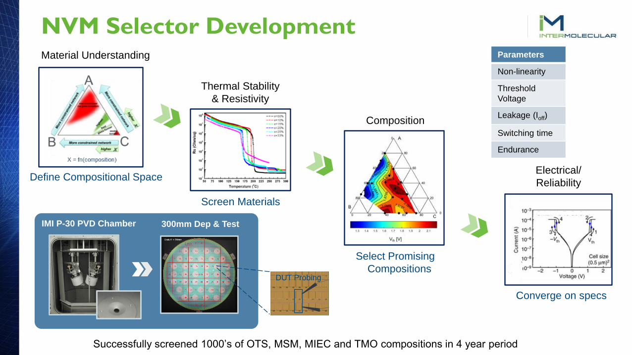
Thermal Stability
& Resistivity
Electrical/
Reliability
Composition
Successfully screened 1000’s of OTS, MSM, MIEC and TMO compositions in 4 year period
Define Compositional Space
Converge on specs
Material Understanding
Screen Materials
Select Promising
Compositions
Parameters
Non-linearity
Threshold
Voltage
Leakage (Ioff)
Switching time
Endurance
Aperture for
site-isolation
IMI P-30 PVD Chamber 300mm Dep & Test
DUT Probing
NVM Selector Development
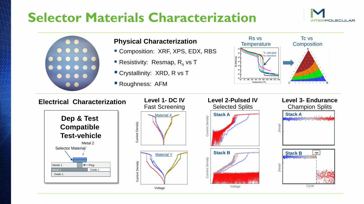
Selector Materials Characterization
Dep & Test
Compatible
Test-vehicle
Metal 1
Nitride 1
Oxide 2
Oxide 1
Plug
Selector Material
Metal 2 Curr
ent
Density
Material X
Curr
ent
Density
Voltage
Material Y
Level 1- DC IV Fast Screening
Physical Characterization
Composition: XRF, XPS, EDX, RBS
Resistivity: Resmap, Rs vs T
Crystallinity: XRD, R vs T
Roughness: AFM
Rs vs Temperature
Tc vs Composition
Level 3- Endurance Champion Splits
Level 2-Pulsed IV Selected Splits
Stack A
Stack B
Voltage
Curr
ent
Density
Curr
ent
Density Stack A
Stack B
Cycle
Jre
ad
Jre
ad
Electrical Characterization

NVM Selector: 3D XPoint
22 Source: http://www.anandtech.com/show/11454/techinsights-publishes-preliminary-analysis-of-3d-xpoint-memory
Size and density most similar to planar NAND
Critical litho for each layer may be cost
disadvantaged vs. 3D NAND type flow with
increasing layer counts

3D Vertical NVM – Conformal Selectors:
Need a conformal selector or self regulating cell (perhaps difficult to realize)
23
Y. Deng, et al, IEEE Int. Electron Devices Meet. (2013), p. 25.7.1–25.7.4.

ALD Chalcogenides (ChG)
Key challenges
Chalcogenides are used in advanced NVM applications
3D Vertical NVM architecture requires highly conformal
deposition processes (e.g. ALD)
Layered binaries require uniform composition and
interface control
ALD chalcogenide chemistry is complex and not well
understood (i.e. not as simple as reactions with O3 or
NH3)
Elemental ALD is desirable to adjust stoichiometry of
base system as memory/selector behavior is
composition dependent
Simplest chemistry is desired which also achieves
performance requirements (e.g. stoichiometry, step
coverage, thermal stability, electrical performance)
A-30 300mm ALD chamber with
in-situ spectroscopic ellipsometry
In-situ ALD Te growth monitoring on SiO2
Time

ALD Chalcogenide Selector Screening
Electrical
Electrical Response
Feedback to Refine
Material Selection
Screen ligands/Develop ALD Unit Processes
Select Promising Compositions
(Leverage PVD Data/Modelling)
Parameter
Non-linearity
Threshold
Voltage
Leakage (Ioff)
Switching time
Endurance
Test ALD Stacks and
Nanolaminates
Thermal Stability
& Resistivity
Process Development and
Materials Characterization
IMI A-30 ALD Chamber
In-situ SE
L(Se,Te) + R (Se,Te) + RL ….etc.
74

ALD Chalcogenide (ChG) Approach
~40:1 AR
R. Gordon, 2014
ALD GeTe31nm x 84nm via
Univ Helsinki,
& IBM, 2011
Example ALD ChG rxn pathways from
literature to form binaries:
(R3Si)2Te(g) + GeCl2(g)
GeTe(s) + 2R3SiCl(g)
ALD GeS
ALD GeTe
(R3Si)2Te(g) + reactant screening
ALD Te
Surface oxide
Example elemental ALD ChG under
investigation at Intermolecular:

ALD Chalcogenide Selector Initial Results
27
80° Tilt
200 nm
Voltage (V)
Vth+Vth-
First fire/
forming
event
Cycle 1
Cycle 2
Cycle 3
• ALD Chalcogenide Selector; elemental ALD to adjust composition of compound
• Conventional TiN Electrodes
• Pulse-mode electrical test (pulse width = 100 ns) shows clear, repeatable selector operation on 350 nm CD devices with forming event visible during first cycle
• Selector threshold voltage between 1.4-1.6V
Top
Mid
Bottom
• Elemental ALD Chalcogenide• Deposition rate ~1 Å/cycle
• 250nm, 24:1 AR trench structures
Cu
rre
nt (A
)
Noise Floor
100ns Pulse IV
ALD Chalcogenide Selector Initial Results
28
80° Tilt
200 nm
Voltage (V)
Vth+Vth-
• ALD Chalcogenide Selector; elemental ALD to adjust composition of compound
• Conventional TiN Electrodes
• Pulse-mode electrical test (pulse width = 100 ns) shows clear, repeatable selector operation on 350 nm CD devices with forming event visible during first cycle
• Selector threshold voltage between 1.4-1.6V
Top
Mid
Bottom
• Elemental ALD Chalcogenide• Deposition rate ~1 Å/cycle
• 250nm, 24:1 AR trench structures
Lo
g C
urr
en
t (A
)
Noise Floor
350 nm device size,100ns Pulse IV,similar composition

Summary
Thin film HfO2 based ferroelectric materials can enable advanced NVM and logic devices
FE performance can be enhanced through stack design, composition tuning, and
structure control
3D NVM architectures will require series connected non-linear selector elements
A conformal selector with layer by layer compositional control can open up potential
integration schemes and provide additional materials engineering control
Initial feasibility using ALD Chalcogenide selectors with good conformality and similar
electrical performance to PVD demonstrated
29

30

Zr Rich Ferroelectric “Antiferroelectric Like”Transition
• Bottom electrode choice can enable ferroelectric response in more Zr rich solid solutions after “wake-up”
Bottom Electrode can be used to tune FEAFE transition composition after field cycling
Hf0.22Zr0.78O2
PVD TiN
ALD TiN
Hf0.22Zr0.78O2
PVD TiN
ALD Ir
Before Wake-up After Wake-upPole Figure at 2θ=30° t/o (111)
• Bottom electrode
imparts some amount
of texture
• Minimal impact on
AFE vs FE response
before wakeup
S. Weeks, et al., “Engineering of Ferroelectric HFO2/ZrO2 Nanolaminates”, ACS Applied Materials & Interfaces (2017, submitted)
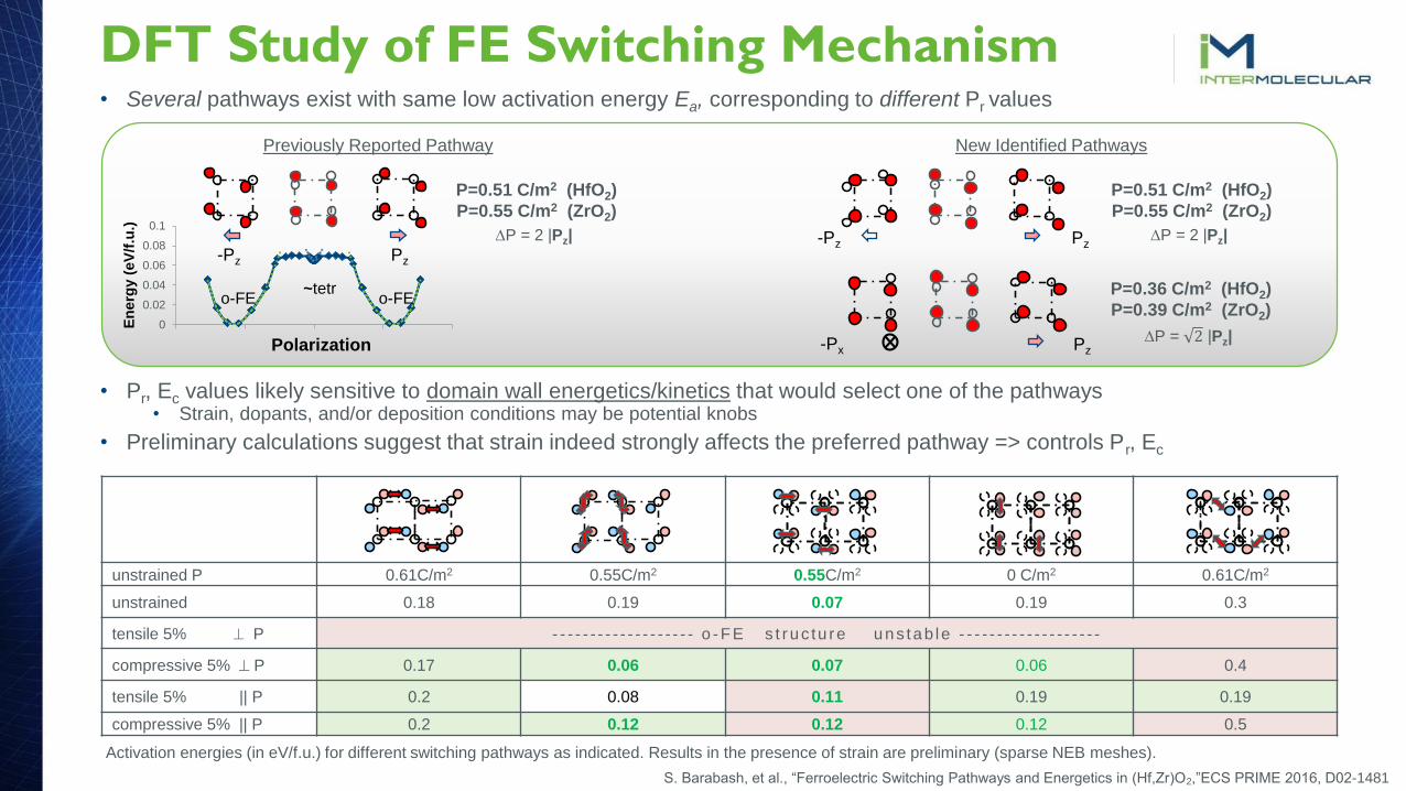
• Several pathways exist with same low activation energy Ea, corresponding to different Pr values
• Pr, Ec values likely sensitive to domain wall energetics/kinetics that would select one of the pathways• Strain, dopants, and/or deposition conditions may be potential knobs
• Preliminary calculations suggest that strain indeed strongly affects the preferred pathway => controls Pr, Ec
DFT Study of FE Switching Mechanism
Previously Reported Pathway
P=0.51 C/m2 (HfO2)
P=0.55 C/m2 (ZrO2)
P = 2 |Pz|
0
0.02
0.04
0.06
0.08
0.1
o-FEo-FE~tetr
Pz-Pz
Polarization
En
erg
y (
eV
/f.u
.)
P=0.36 C/m2 (HfO2)
P=0.39 C/m2 (ZrO2)
P = 2 |Pz|Pz-Px
New Identified Pathways
Pz-Pz
P=0.51 C/m2 (HfO2)
P=0.55 C/m2 (ZrO2)
P = 2 |Pz|
unstrained P 0.61C/m2 0.55C/m2 0.55C/m2 0 C/m2 0.61C/m2
unstrained 0.18 0.19 0.07 0.19 0.3
tensile 5% P - - - - - - - - - - - - - - - - - - - o - FE s t r uc tu re uns tab le - - - - - - - - - - - - - - - - - - -
compressive 5% P 0.17 0.06 0.07 0.06 0.4
tensile 5% || P 0.2 0.08 0.11 0.19 0.19
compressive 5% || P 0.2 0.12 0.12 0.12 0.5
Activation energies (in eV/f.u.) for different switching pathways as indicated. Results in the presence of strain are preliminary (sparse NEB meshes).
S. Barabash, et al., “Ferroelectric Switching Pathways and Energetics in (Hf,Zr)O2,”ECS PRIME 2016, D02-1481

33
Selector Examples
D. Kau et al, IEDM09S. H. Jo et al, TED15A. Padilla et al, TED15
Memory selector elements based on different material systems and physical mechanisms
MIEC ChalcogenidesFAST