chapter 8 : transistor biasing and thermal...
TRANSCRIPT

Basic Electronics (GTU) 8-1 Transistor Biasing & Thermal Stability
Chapter 8 : Transistor Biasing and Thermal Stability
Section 8.5 :
Ex. 8.5.2 : The fixed bias circuit of Fig. P. 8.5.2 uses a silicon transistor. The component values are
RC = 500 and RB = 100 k. dc of the transistor is 100 at 30C and increases to 120 at
a temperature of 80C. Determine the percent change in the Q point values over this
temperature range. Assume that VBE and ICBO remain constant. .Page No. 8-10.
Fig. P. 8.5.2
Soln. :
Steps to be followed :
Step 1 : Obtain the Q point at 30C.
Step 2 : Obtain the Q point at 80C.
Step 3 : Calculate the percent change in Q point values.
Step 1 : To obtain the Q point at 30C :
Obtaining Q point values means to calculate VCEQ and ICQ. Let us use dc = 100.
Applying KVL to the base circuit of Fig. P. 8.5.2 we get,
VCC – IB RB – VBE = 0
IB = VCC – VBE
RB
= 12 – 0.7
100 103 = 113 A ...(1)
Now neglecting ICEO we can write,
ICQ = dc IB = 100 113 10– 6
= 11.3 mA ...(2)
Apply KVL to the collector circuit of Fig. P. 8.5.2 to get,
VCC – VCEQ – ICQ RC = 0
VCEQ = VCC – ICQ RC = 12 – (11.3 10– 3
500) = 6.35 V ...(3)
Thus the Q point co-ordinates at 30C are :
Q point at 30C = (VCEQ, ICQ) = (6.35 V, 11.3 mA)

Basic Electronics (GTU) 8-2 Transistor Biasing & Thermal Stability
Step 2 : To obtain the Q point at 80C :
Let us use dc = 120. Now from Equation (1), IB = 113 A.
Therefore the new value of ICQ is given by,
ICQ (80C) = dc IB = 120 113 10– 6
ICQ (80C) = 13.56 mA ...(4)
Applying KVL to collector circuit we get,
VCEQ (80C) = VCC – ICQRC = 12 – (13.56 10– 3
500)
VCEQ (80C) = 5.22 V ....(5)
Thus the Q point values at 80C are :
Q point at 80C = (VCEQ, ICQ) = (5.22 V, 13.56 mA)
Step 3 : To calculate percent change in Q point values :
Percent change in ICQ = ICQ (80C) – ICQ (30C)
ICQ (30C) 100%
= 13.56 – 11.3
11.3 100%
Percent change in IC = 20% (increase) ...Ans.
Percent change in VCEQ = VCEQ (80C) – VCEQ (30C)
VCEQ (30C) 100% =
5.22 – 6.35
6.35 100%
Percent change in VCEQ = – 17.79% (decrease) ...Ans.
Ex. 8.5.3 : Derive the expression for the stability factor “S” of a fixed bias circuit. Comment on the
result. .Page No. 8-10.
Soln. :
We have defined the stability factor “S” as follows :
S = IC
ICO
constant VBE and dc
S gives us the change in IC due to change in the reverse saturation current ICBO. As ICBO changes
by ICBO, the base current IB will change by IB and the collector current IC changes by IC.
For a CE configuration we know that,
IC = dc IB + ICEO = dc IB + (1 + dc) ICBO
Therefore change in IC is given by,
IC = dc IB + (1 + dc) ICBO
Dividing both the sides by IC we get,
1 = dc
IB
IC
+ (1 + dc)
ICBO
IC

Basic Electronics (GTU) 8-3 Transistor Biasing & Thermal Stability
1 – dc
IB
IC
= (1 + dc)
ICBO
IC
ICBO
IC
= 1 – dc [ IB / IC ]
(1 + dc)
But, S = IC
ICBO
S = (1 + dc)
1 – dc [ IB / IC ] ...(8.5.5)
But for the fixed bias circuit,
IB = VCC – VBE
RB
In this equation VCC, VBE and RB all are fixed. Therefore IB cannot change. IB = 0.
Substituting this in Equation (8.5.5) we get,
S = (1 + dc) ...(8.5.6)
Comment on the expression for S :
Substitute dc = 49 in Equation (8.5.6). The value of S = 50. i.e. collector current change is 50
times as large as change in the reverse saturation current ICBO. Fixed bias circuit thus gives a very poor
stability of the Q point. It is the worst configuration as far as the stability of Q point is concerned.
Ex. 8.5.4 : Derive the expression for the stability factor S of a fixed bias circuit. Also derive the
relation between S and S for the same. .Page No. 8-10.
Soln. :
We have defined the stability factor S as
S = IC
VBE
constant ICO and dc
For a common emitter configuration, we have
IC = dc IB + (1 + dc) ICO ...(1)
We will substitute IB in terms of VBE into Equation (1).
For this, refer Fig. P. 8.5.4 and apply KVL to get,
VCC = IB RB + VBE ...(2)
IB = VCC – VBE
RB
...(3) Fig. P. 8.5.4 : Base loop
Substitute Equation (3) into Equation (1) to get,
IC = dc
VCC – VBE
RB
+ (1 + dc) ICBO
Note that ICO and ICBO are one and the same.
IC RB = dc VCC – dc VBE + (1 + dc) ICBO RB ...(4)

Basic Electronics (GTU) 8-4 Transistor Biasing & Thermal Stability
Differentiate this expression with respect to VBE to get,
RB IC
VBE
= 0 – dc + 0
RB S = – dc
S = – dc
RB
...(8.5.7)
This is the required expression. The negative sign indicates that IC decreases as temperature
increases due to reduction in VBE at increased temperature.
Relation between S and S :
We have already derived the expression for S as S = (1 + dc). In this expression substitute
dc = – S RB to get,
S = 1 – S RB
or S = (1 – S)
RB
This is the required relation.
Ex. 8.5.5 : Derive the expression for the stability factor S for a fixed bias circuit. .Page No. 8-10.
Soln. :
We have already defined the stability factor S as
S = IC
dc
ICO and VBE constant
For a common emitter configuration.
IC = dc IB + (1 + dc) ICBO
= dc IB + dc ICBO + ICBO
Differentiate both sides partially with respect to dc we get,
IC
dc
= IB + ICBO + 0
Neglecting ICBO we get,
S = IC
dc
= IB = IC
dc
S = IC
dc
…(8.5.8)
This is the required expression.
Note : Out of S, S and S the stability factor S is significantly higher than the remaining two.

Basic Electronics (GTU) 8-5 Transistor Biasing & Thermal Stability
Ex. 8.5.6 : Calculate the stability factor S for the fixed bias circuit shown in Fig. P. 8.5.6.
.Page No. 8-10.
Fig. P. 8.5.6
Soln. :
The stability factor S for the fixed bias circuit is given by : S = 1 + dc
Therefore we must find the value of dc.
But dc = IC
IB
So we have to obtain the values of IC and IB.
We know that,
IC = VCC – VCE
RC
= 12 – 6
1 k
= 6 mA
And IB = VCC – VBE
RB
= 12 – 0.7
100 k = 113 A
Therefore, dc = IC
IB
= 6 10
– 3
113 10– 6 = 53.09
Hence the stability factor S = 1 + 53.09 = 54.1 ...Ans.
Ex. 8.5.8 : For the device characteristics shown in Fig. P. 8.5.8(a) calculate VCC, RB and RC for the
fixed bias circuit of Fig. P. 8.5.8(b). .Page No. 8-12.
(a) (b)
Fig. P. 8.5.8

Basic Electronics (GTU) 8-6 Transistor Biasing & Thermal Stability
Step 1 : Find VCC and IC (max) :
From the dc load line of Fig. P. 8.5.8(a) we get,
VCC = 15 V and IC (max) = 10 mA
Step 2 : Calculate RB and RC :
RB = VCC – VBE
IBQ
= 15 – 0.7
50 A = 286 k …Ans.
RC = VCC
IC (max)
= 15
10 mA = 1.5 k …Ans.
Section 8.7 :
Ex. 8.7.3 : A Si transistor used in self bias has VCC = 20 V, RC = 2 k. The nominal operating point
is VCE = 10 V and IC = 4 mA. If = 50, Calculate R1, R2 and RE if stability factor S = 10 is
desired. If S 3 is required, what will be the price paid for achieving this stability ? Refer
Fig. P. 8.7.3(a). .Page No. 8-23.
Fig. P. 8.7.3(a)
Soln. :
Steps to be followed :
Step 1 : Calculate IB.
Step 2 : Apply KVL to the collector loop and calculate RE.
Step 3 : Using the expression for “S” calculate RB i.e. R1 || R2.
Step 4 : Calculate the values of R1 and R2.
Step 1 : Calculate IB :
IB = IC / dc = 4 10
– 3
50 = 80 A ...(1)
Step 2 : Apply KVL to the collector loop and calculate RE :
VCC = IC RC + VCE + IE RE = IC RC + VCE + (IC + IB) RE ...Ans.
RE = VCC – VCE – IC RC
(IC + IB) =
20 – 10 – (4 2)
(4.08 10– 3
) = 490.2

Basic Electronics (GTU) 8-7 Transistor Biasing & Thermal Stability
Step 3 : Calculate RB :
The expression for stability factor of “S” for self bias circuit is given by,
S = (1 + dc) 1 + (RB / RE)
(1 + dc) + (RB / RE) ...(2)
S = (1 + 50) [1 + (RB / 490)]
(1 + 50) + (RB / 490) = 10
51 + 51 RB
490 = 510 +
10 RB
490
41 RB
490 = 459
RB = 5.485 k …Ans.
But, RB = R1 || R2 = R1 R2
(R1 + R2)
R1 R2
(R1 + R2) = 5.485 k ...(3)
R2
(R1 + R2) =
5.485 103
R1
...(4) Fig. P. 8.7.3(b)
Step 4 : To calculate the values of R1 and R2 :
The Thevenin’s equivalent circuit is as shown in Fig. P. 8.7.3(b).
Apply KVL to the base loop to write,
VTH – IB RB – VBE – IE RE = 0
But IB = 80 A and IE = (1 + ) IB = 51 80 10– 6
= 4.08 mA
Substituting the values we get,
VTH – 80 10– 3
5.485 – 0.7 – 4.08 0.4902 = 0
VTH = 3.17 Volts
But VTH = R2
(R1 + R2) VCC
R2
R1 + R2
= 3.17
20 = 0.158
R2 VCC
R1 + R2
= 3.17
and RB = R1 R2
R1 + R2
= 5.485 103
Substituting the value of R2
R1 + R2
= 0.158 into expression for RB we get
R1 0.158 = 5.485 103
R1 = 34.7 k ...Ans.

Basic Electronics (GTU) 8-8 Transistor Biasing & Thermal Stability
R2
R2 + 34.7 = 0.158
R2 = 0.158 R2 + 5.4826
R2 = 5.4826 k
0.842 = 6.51 k ...Ans.
Effect of reducing S to 3 :
If S 3 then,
(1 + ) 1 + (RB / RE)
1 + + (RB / RE) 3
51 [1 + (RB / 490 )]
51 + (RB / 490) 3
For S = 3, 51 + 51 RB
490 = 153 +
3 RB
490
RB = 1.041 k for S = 3.
The effect is reduction in the input impedance. Thus the stabilization is improved at the cost of
reduced input impedance.
Ex. 8.7.4 : The silicon transistor shown in Fig. P. 8.7.4 has = 99, IBQ = 30 A, VBEQ = 0.7V. Find R2
and VCEQ. .Page No. 8-23.
Fig. P. 8.7.4
Soln. :
Step 1 : Calculate IC :
IC = IB = 99 30 10– 6
= 2.97 mA ...(1)
Step 2 : Calculate VCE :
Apply KVL to collector circuit to write :
VCC = IC RC + VCE + (IC + IB) RE
VCE = VCC – IC (RC + RE) – IB RE
= 15 – 2.97 (2 + 1) – 30 10– 6
1 103 = 6.06 V ...Ans.
Step 3 : Calculate the value of R2 :
Apply KVL to the base-emitter loop to write,
VR2 = VBE + IE RE = VBE + (1 + ) IB RE
VR2 = 0.7 + (100 30 10– 6
1 103) = 3.7 V

Basic Electronics (GTU) 8-9 Transistor Biasing & Thermal Stability
But, VR2 = R2
(R1 + R2) VCC ... Using approximate analysis
3.7 = 15 R2
R1 + R2
3.7 R1 + 3.7 R2 = 15 R2
R2 = 3.7 R1
11.3 = 3.27 k ...Ans.
Ex. 8.7.5 : Derive the expression for the stability factor S of the voltage divider bias circuit. Comment
on the result. .Page No. 8-23.
Soln. :
To derive the expression for S we are going to use the same equation which we had used to
obtain “S” for the collector to base bias which is,
S = 1 + dc
1 – dc [ ]IB/IC
…(1)
and substitute the value of IB
IC
for the self bias circuit to obtain the required expression for S.
To obtain the value of IB / IC :
Consider the Thevenin’s equivalent circuit which we have discussed in section 8.7.5. The same
circuit has been repeated in Fig. P. 8.7.5.
Apply KVL to the base circuit of Fig. P. 8.7.5 we can write,
VTH = IR RB + VBE + (IC + IB) RE …(2)
If we consider to be independent of, we can differentiate Equation (2) with respect to IC to obtain,
0 = RB IB
IC
+ 0 + RE + RE IB
IC
0 = IB
IC
(RB + RE) + RE
IB
IC
= – RE
(RB + RE) …(3)
IB
IC
= – RE
(RB + RE)
Substitute this in Equation (1) to obtain,
Fig. P. 8.7.5 : Thevenin’s equivalent circuit
for voltage divider bias circuit
S = 1 + dc
1 – dc
– RE
RB + RE
S = 1 + dc
1 + dc
RE
RB + RE
…(4)

Basic Electronics (GTU) 8-10 Transistor Biasing & Thermal Stability
S = (1 + dc) (RB + RE)
RB + RE + dc RE
= (1 + dc) (RB + RE)
RB + (1 + dc) RE
Divide numerator and denominator by RE to get,
S = (1 + dc) 1 + (RB/RE)
(1 + dc) + (RB/RE) …(5)
This is the desired result.
Comments on the result :
The value of S depends on the ratio (RB/RE). If RB/RE is small then the value of S = 1 and if the
ratio (RB/RE) then S (1 + dc). Thus the self bias circuit is more stable for smaller values
of the ratio (RB/RE).
If the ratio (RB/RE) is fixed then S increases with increase in the value of dc. Thus stability
decreases with increase in dc.
S is independent of dc for small values of dc.
Smaller values of RB give better stabilization.
Ex. 8.7.7 : The transistor shown in the circuit in the
Fig. P. 8.7.7 has hFE = 50 at 25 C and
hFE = 200 at 75 C. Reverse saturation
current ICO = 0.01 A at with 25 C a
temperature coefficient of 7%C and
VBE = 0.7 V at 25. Temperature
coefficient of VBE is – 2.5 mV/C.
Calculate : 1. Quiescent currents 2.
Quiescent collector current drift at 75C.
.Page No. 8-24.
Fig. P. 8.7.7 : Given circuit
Soln. :
Steps to be followed :
Step 1 : Calculate the values of IB and IC at 25C.
Step 2 : Calculate the changes in ICO, and VBE with temperature.
Step 3 : Calculate the values of S, S and S.
Step 4 : Obtain the value of IC = S ICBO + S VBE + S
Step 1 : Calculate IB and IC at 25 C :
By applying KVL around base loop, we get,
– 1 + IB RB + VBE + (IB + IC) RE = 0
IB = 1 – 0.7
RB + 1(1 + ) RE
= 1 – 0.7
1 k + 51 100 = 49 A …(1)
IC = IB = 50 49 A = 2.45 mA …(2)
Step 2 : Changes in hFE , ICO and VBE :
From the data, the changes in different parameters are as follows :

Basic Electronics (GTU) 8-11 Transistor Biasing & Thermal Stability
hFE () ICO VBE
25 C 50 0.01 A 0.7
75 C 200 0.32 A 0.575
Hence, = hFE2 – hFE1 = 200 – 50 = 150
ICO = ICO2 – ICO1 = 0.32 – 0.01 = 0.31 A
VBE = 0.575 – 0.7 = – 0.125 V
Step 3 : Calculate the values of S, S and S :
S = (1 + ) 1 + [RB / RE]
1 + + [RB / RE]
S = (1 + 50) 1 + [1 / 0.1]
1 + 50 + [1 / 0.1] = 9.2
S =
– / RE
1 + + [RB / RE] =
– 50 / 100
1 + 50 + [1 / 0.1] = – 8.196 10
– 3
S =
SIC
(1 + ) =
9.2 2.45 10– 3
50 (1 + 50) = 8.84 10
– 6
Step 4 : To calculate change in IC :
IC = S ICO + S VBE + S
= (9.2 0.31 10– 6
) – (8.196 10– 3
– 0.125)
+ (8.84 10– 6
150)
IC = 2.852 A + 1.0245 mA + 1.326 mA = 2.3533 mA ...Ans.
So new value of IC = 2.45 + 2.3533 = 4.8033 mA ...Ans.
Section 8.11 :
Ex. 8.11.3 : The reverse saturation current of germanium transistor in Fig. P. 8.11.3(a) is 2 A at room
temperature and increases by a factor of 2 for each temperature increase of 10C. The
bias VBB = 5V. Find the maximum allowable value of RB if the transistor is to remain cutoff
at a temperature of 75C. .Page No. 8-39.
(a) Given circuit (b) Input loop
Fig. P. 8.11.3

Basic Electronics (GTU) 8-12 Transistor Biasing & Thermal Stability
Soln. :
Step 1 : Value of ICBO at 75 C :
Let the room temperature be 25C.
at 25C : ICBO = 2 A
ICBO doubles for every 10C increase in temperature.
at 75C : ICBO = 64 A.
Step 2 : Calculate value of RB :
In order to keep the transistor off, it is necessary to keep VBE – 0.1 V.
Refer Fig. P. 8.11.3(b) and apply KVL to the input loop to get,
VBB + VBE = ICBO RB
VBE = – VBB + RB ICBO – 0.1
– 5 + (RB 128 10– 3
) – 0.1
RB 4.9
128 10– 6
RB 38.28 k or RBmax = 38.28 k ...Ans.
Ex. 8.11.4 : Fig. P. 8.11.4, a circuit using p-n-p germanium
transistor with dc = 150 and ICO = 2.5 mA.
The quiescent collector current is 500 mA Find :
(a) The value of resistor RB.
(b) The largest value of that can result in
a thermally stable circuit. Page No. 8-40.
Soln. :
Given : dc = 150, ICO = 2.5 mA, ICQ = 500 mA.
Step 1 : Calculate RB :
1. Calculate IB
IC = IB + (1+ ) ICO
500 = 150 IB + (151 2.5)
IB = 0.816 mA ...(1) Fig. P. 8.11.4
2. Apply KVL to the base emitter circuit to write,
VCC = IB RB + VEB + IE RE
20 = 0.816 10– 3
RB + 0.3 + (IC + IB) RE
RB = 20 – 0.3 – (500.816 10
– 3 5)
0.816 10– 3
= 21.073 k ...Ans.
3. Calculate VEC
VCC = (IC 10) + VEC + IE 5
VEC = VCC – 10 IC – 5 IE = 20 – (10 0.5) – (5 0.500816)
VEC = 12.49 V
Basic Electronics (GTU) 8-13 Transistor Biasing & Thermal Stability
VCE = – 12.49 V
As | VCE | > | VCC/2 | the circuit of Fig. P. 8.11.4 is not inherently stable.
Step 2 : Calculate the stability factor (S) :
S = (1 + ) 1 + (RB/RE)
1 + + (RB/RE)
S = (151)
1+ (21.073 10
3/5)
151 + (21.073 103/5)
= 145.8
Step 3 : Calculate :
Substitute “S” in the following equation :
[VCC – 2 IC (RE + RC)] (S) (0.07 ICO) < 1
[20 – 2 0.5 (5 + 10)] (145.8 0.07 2.5 10 – 3
) < 1
0.1275 < 1
< 7.84 C/W max = 7.84 C/W.
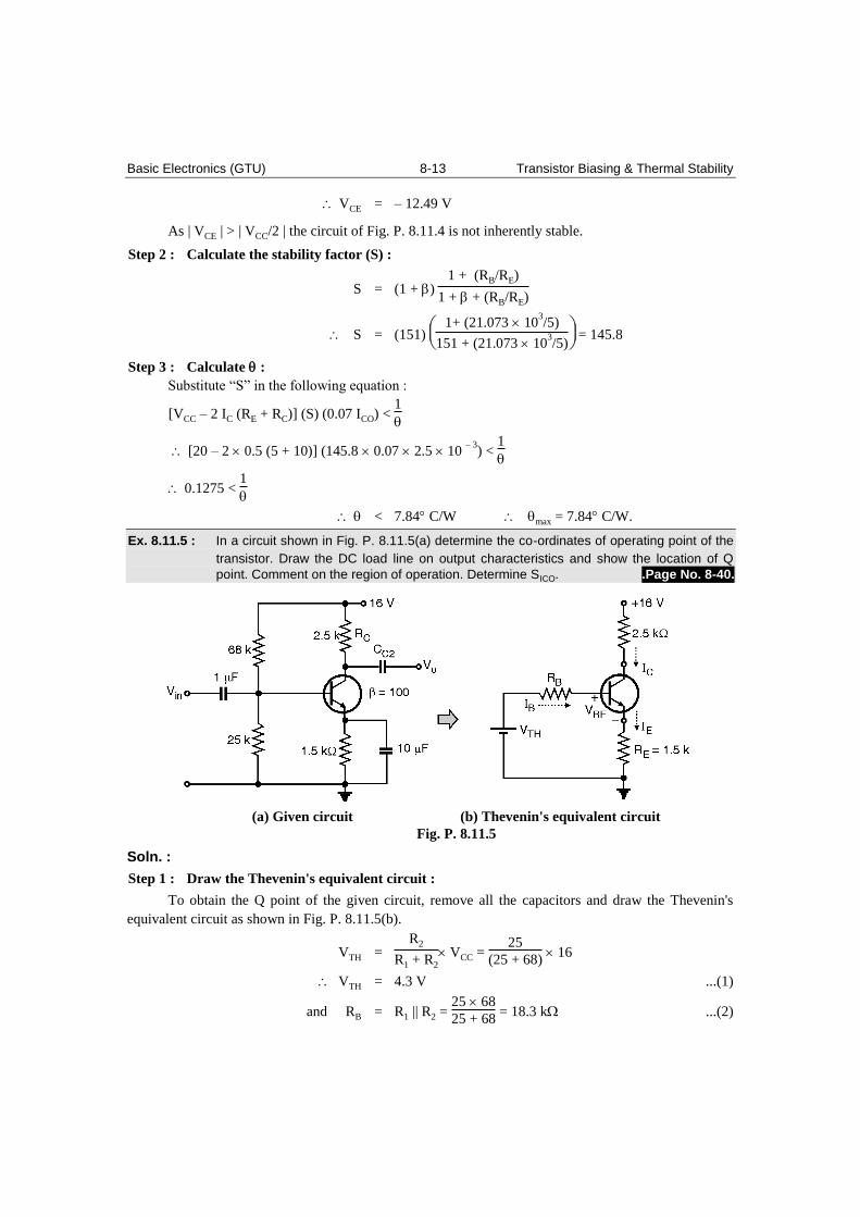
Ex. 8.11.5 : In a circuit shown in Fig. P. 8.11.5(a) determine the co-ordinates of operating point of the
transistor. Draw the DC load line on output characteristics and show the location of Q
point. Comment on the region of operation. Determine SICO. .Page No. 8-40.
(a) Given circuit (b) Thevenin's equivalent circuit
Fig. P. 8.11.5
Soln. :
Step 1 : Draw the Thevenin's equivalent circuit :
To obtain the Q point of the given circuit, remove all the capacitors and draw the Thevenin's
equivalent circuit as shown in Fig. P. 8.11.5(b).
VTH = R2
R1 + R2
VCC = 25
(25 + 68) 16
VTH = 4.3 V ...(1)
and RB = R1 || R2 = 25 68
25 + 68 = 18.3 k ...(2)

Basic Electronics (GTU) 8-14 Transistor Biasing & Thermal Stability
Step 2 : Calculate IB :
Apply KVL to the base loop of Fig. P. 8.11.5(b) to write,
VTH – IB RB – VBE – IE RE = 0
VTH – IB RB – VBE – (1 + ) IB RE = 0
IB = VTH – VBE
[RB + (1 + ) RE] =
4.3 – 0.7
[18.3 + (101 1.5)] 103
IB = 2.12 10– 5
A
Step 3 : Calculate ICQ :
ICQ = IB = 100 2.12 10– 5
= 2.12 mA
Step 4 : Calculate VCEQ :
VCEQ = VCC – IC RC – IE RE
But IE = (1 + ) IB = 101 2.12 10– 5
= 2.1412 10– 3
= 16 – (2.12 2.5) – (2.1412 1.5) = 7.4882 Volts.
Hence the Q-point is given by : (7.4882 V, 2.12 mA) ...Ans.
Step 5 : To draw the load line and locate Q point :
Fig. P. 8.11.5(c) : Load line and Q-point
The load line is as shown in Fig. P. 8.11.5(c). The two extreme points A and B are given by,
Point A : IC max = VCC / (RC + RE) = 16
(2.5 + 1.5) 103 = 4 mA.
Point B : Corresponds to VCE = VCC = 16 V.
Region of operation : Active Region
Step 6 : Calculate SICO :
SICO is S, and the expression for S of a voltage divider bias circuit is given by,
S = (1 + ) 1 + (RB / RE)
(1 + ) + (RB / RE)
S = (1 + 100) 1 + [18.3 / 1.5]
(1+ 100) + (18.3 / 1.5) = 11.78 ...Ans.

Basic Electronics (GTU) 8-15 Transistor Biasing & Thermal Stability
Ex. 8.11.6 : A p-n-p germanium transistor is used in the self biasing arrangement with
VCC = 5V, R1 = 27k, R2 = 3k, RE = 270 , RC = 2k and = 50.
Find VCEQ and ICQ. .Page No. 8-40.
Soln. :
Given : VCC = 5V, R1 = 27 , R2 = 3, RE = 270 , RC = 2 and = 50.
Step 1 : Draw the circuit :
The circuit is as shown in Fig. P. 8.11.6(a).
Step 2 : Draw Thevenin's equivalent circuit :
Thevenin's equivalent circuit is shown in Fig. P. 8.11.6(b), in which
VTH = R2
R1 + R2
VCC = 3
27 + 3 – 5 = 0.5 volts
RB = R1 || R2 = 27 3
27 + 3 = 2.7 k
(a) Given circuit (b) Thevenin's equivalent circuit
Fig. P. 8.11.6
Step 3 : Calculate IB, IC and VCE :
Apply KVL to the base loop of Fig. P. 8.11.6(c) to write,
VTH = IE RE + VEB + IB RB
But IE = (1 + ) IB
VTH – VEB = (1 + ) IB RE + IB RB
IB = VTH – VEB
RB + (1 + ) RE
= 0.5 – 0.3
2.7 k + (51 0.27 k) = 13 A
(c) Base loop (d) Collector loop Fig. P. 8.11.6

Basic Electronics (GTU) 8-16 Transistor Biasing & Thermal Stability
Collector current, IC = IB = 50 13 10– 6
= 0.63 mA ...Ans.
Apply KVL to the collector loop of Fig. P. 8.11.6(d) to get,
VCC = IE + RE + VEC + IC RC
VEC = VCC – IE RE – IC RC = 5 – (1+ ) IB RE – IC RC
= 5 – 51 13 10– 6
270 – 0.63 10– 3
2 103
VEC = 5 – 0.18 – 1.3 = 3.5 V
VCE = – VEC = – 3.5 V ...Ans.
Ex. 8.11.7 : For the biasing arrangement as shown in Fig. P. 8.11.7, assume that the reverse
saturation currents of diode and transistor are equal. Show that :
S = IC
ICO
= 1 and S = – dc
R1 .Page No. 8-40.
Soln. :
Assumptions :
1. The diode D is made of same material as that of the
transistor.
2. The reverse saturation current of the diode i.e. Io is
equal to the reverse saturation current of the transistor
i.e. ICO.
Io = ICO
To prove that S = 1 :
Looking at Fig. P. 8.11.7 we can write that, Fig. P. 8.11.7 : Given circuit
IB = I1 – Io ...(1)
The collector current IC is given as :
IC = dc IB + (1 + dc) ICO ...(2)
Substitute the value of IC from Equation (1) to get :
IC = dc (I1 – Io) + (1 + dc) ICO
IC = dc I1 – dc I0 + ICO + dc ICO ...(3)
But Io = ICO
IC = I1 dc + ICO ...(4)
S = IC
ICO
= 0 + 1
S = 1 Proved ...Ans.

Basic Electronics (GTU) 8-17 Transistor Biasing & Thermal Stability
To prove that S = – dc
R1
:
S is defined as : S = IC
VBE
ICO
and dc
costants
Consider the base circuit of Fig. P. 8.11.7 and apply KVL to write,
VCC = I1 R1 + VBE
I1 R1 = VCC – VBE
I1 = VCC – VBE
R1
...(5)
But from Equation (4),
IC = I1 dc + ICO
Substituting value of I1 we get,
IC = (VCC – VBE) dc
R1
+ ICO
= VCC
R1
– dc
R1
VBE + ICO
As dc and ICO are assumed to be constants,
S = IC
VBE
= 0 – dc
R1
+ 0
S = – dc
R1
...Proved. ...Ans.
Ex. 8.11.8 : For the circuit shown in Fig. P. 8.11.8(a).
Determine : 1. IC 2. VC 3. VE 4. VCE Assume dc = 100. .Page No. 8-41.
Fig. P. 8.11.8(a)

Basic Electronics (GTU) 8-18 Transistor Biasing & Thermal Stability
Soln. :
Step 1 : Draw the dc equivalent circuit :
For dc analysis all the capacitors offer infinite
impedance. Hence they are replaced by open circuit in
the dc equivalent circuit of Fig. P. 8.11.8(b).
The 470 k and 220 k resistances will appear in series
with each other in the dc equivalent circuit.
Step 2 : To obtain the base current IBQ and ICQ :
Applying the KVL to the base circuit of Fig. P. 8.11.8(b) we
can write,
VCC = (IC + IB) RC+ IBRB+ VBE + IERE ...(1)
IB (RB + RC) = VCC – VBE – IERE – ICRC ...(2)
Fig. P. 8.11.8(b) : Simplified circuit
for dc analysis
But, IC = dc IB and IE = ( 1 + dc ) IB
Substituting these values in Equation (2) we get,
IB ( RB+ RC ) = VCC – VBE – ( 1 + dc) IB RE – dc IB RC
IB [RB + RC + (1 + dc ) RE + dc RC] = VCC – VBE
IB = VCC – VBE
[RB + (1 + dc) RC + (1 + dc) RE ] ...(3)
Substituting the values we get,
IB = 30 – 0.7
[690 + ( 101 6.2) + ( 101 1.5) ] 103
IBQ = 19.96 A ≈ 20 µA ...(4)
Collector current ICQ = dc IBQ = 100 20 10– 6
ICQ = 2 mA ...Ans.
The emitter current IE = ( 1 + dc ) IB = 101 20 10– 6 = 2.02 mA ...(5)
Step 3 : To calculate VE , VCE and VC :
To calculate VE :
VE = IE RE = 2.02 1.5 VE = 3.03 Volts ...Ans.
To calculate VCE :
Apply KVL to the collector circuit of Fig. P. 8.11.8(b) to write,
VCC = ( IC + IB ) RC+ VCE + VE
VCE = VCC – VE – ( IC + IB ) RC

Basic Electronics (GTU) 8-19 Transistor Biasing & Thermal Stability
Substituting values we get,
VCE = 30 – 3.03 – ( 2.02 6.2 ) = 14.45 Volt ...Ans.
To calculate VC :
VC = VCE + VE
VC = 14.45 + 3.03 = 17.476 Volts ...Ans.
Ex. 8.11.9 : A CE amplifier employing NPN transistor has a load resistance RL connected between
collector and VCC supply of + 16 Volts. For biasing a resistor, R1 is connected between
VCC and base. Resistor R2 = 30 k is connected between base and ground. RE = 1 k.
Draw the circuit diagram. Calculate the value of R1 and RC and stability factor “S” if,
VBE = 0.2, IEQ = 2 mA, VCEQ = 6 Volt, = 0.985. .Page No. 8-41.
Soln. :
Step 1 : Calculate dc and ICQ :
The circuit diagram is as shown in Fig. P. 8.11.9.
Let us first calculate the value of dc.
dc =
(1 – ) =
0.985
1 – 0.985 = 65.67 ...(1)
and ICQ = IE = 0.985 2 = 1.97 mA ...(2)
Step 2 : To obtain the value of RC :
Apply KVL to the collector circuit of Fig. P. 8.11.9
to write,
VCC = ICQ RC+ VCEQ + IEQ RE
RC = VCC – VCEQ – IEQ RE
ICQ Fig. P. 8.11.9
Substituting the values we get,
RC = 16 – 6 – ( 2 1 )
1.97 10– 3 = 4.06 k ...Ans.
Step 3 : To obtain the value of R1 :
Apply KVL to the base circuit of Fig. P. 8.11.9 to write,
VCC = IR1 R1+ VBE + IEQ RE
R1 = VCC – VBE – ( IEQ RE)
IR1 ...(3)
But we do not know IR1.
IR1 = IR2 + IB = VB
R2 +
ICQ
dc
= (IEQ RE+ VBE)
R2 +
ICQ
dc

Basic Electronics (GTU) 8-20 Transistor Biasing & Thermal Stability
IR1 = (2 + 0.2)
30 103 + 1.97 10– 3
65.67 = 103.2 A
Substituting this value in Equation (3) we get,
R1 = 16 – 0.2 – (2 1)
103.2 10– 6 = 133.72 k ...Ans.
RB = R1|| R2 = R1R2
R1+ R2 =
133.72 30
163.72 = 24.50 k ...Ans.
Step 4 : To obtain the stability factor S :
S = 1 + dc
1 + dc
RE
RB+ RE
= 1 + 65.67
1 + 65.67
1
24.50 + 1
= 18.64 ...Ans.
Ex. 8.11.10 : In the self bias circuit shown in Fig. P. 8.11.10(a), R1 = RC = 500 , R2 = 5 k,
RE = 100 10 , hFE = 75, ICBO = 0.2 A and VCC = 20 V.
1. Find an expression for change in ICQ due to change in RE alone.
2. Calculate change in ICQ when RE changes from minimum to maximum value.
All other parameters are constant. .Page No. 8-41.
(a) Given circuit (b) The modified circuit of Fig P. 8.11.10(a)
Fig. P. 8.11.10
Soln. :
Step 1 : The simplified DC equivalent circuit is shown in Fig. P. 8.11.10(b).
Step 2 : Apply KVL around the base loop to obtain expression for VB :
VB = IB RB + VBE + (IB + IC) RE ...(1)
VB = IB (RB + RE) + VBE + IC RE
VB = IB (RB + RE) + VBE + IB RE
VB = IB [RB + (1 + ) RE] + VBE ...(2)

Basic Electronics (GTU) 8-21 Transistor Biasing & Thermal Stability
Step 3 : Get the expression for IC :
We know that, IC = IB + (1 + ) ICBO ...(3)
From Equation (2) we get
IB = VB – VBE
[ RB + (1 + ) RE ]
Now substitute this expression into Equation (3) to get,
IC = [VB – VBE ]
RB + (1 + ) RE
+ (1 + ) ICBO
For >> 1, (1 + )
IC = (VB – VBE)
RB + RE
+ ICBO
= (VB – VBE) + ICBO (RB + RE)
RB + RE
IC = [VB – VBE + ICBO (RB + RE)]
RB + RE
Step 4 : Obtain the stability factor SRE :
Differentiating both sides of the above equation with respect to RE with ICBO, VB and constants
we get stability factor SRE.
IC
RE
= SRE =
( ) RB + RE 2 [ ICBO RB – { VB + RB ICBO – VBE}] ...(4)
Substitute RE = 100 – 10 = 90 , = hFE = 75
RB = R1 || R2 = 500 || 5 k = 454.5
VB = R1
R1 + R2
VCC = 500
500 + 5 k 20V
VB = 1.82 V , ICBO = 0.2 A
Step 5 : Calculate the value of SRE :
Substituting the values into Equation (4) we get,
SRE = 75
[454.5 + (90 75)]2 [ 0.2 10
– 6 454.5 – 75 (1.82 + 454.2 0.2 10
– 6 – 0.7 ]
SRE = – 1.1659 10– 4
A/
This is the value of stability factor.
Step 6 : Obtain IC :
Change in collector current is given by,
IC = SRE RE = – 1.1659 10– 4
(110 – 90)
IC = – 2.3318 mA ...Ans.

Basic Electronics (GTU) 8-22 Transistor Biasing & Thermal Stability
Ex. 8.11.11 : The silicon transistor shown in Fig. P. 8.11.11
has ICBO = 0.5 A, VBE = 0.7 V and = 75 at
room temperature. Calculate the value of ICQ.
If ICBO doubles for every 10 C rise in
temperature and VBE has a temperature
coefficient of 2 mV/C. Calculate value of ICQ if
the temperature rises by 20C. Assume to
be constant. .Page No. 8-42.
Fig. P. 8.11.11
Soln. :
Step 1 : To calculate IB and IC at room temperature :
By applying KVL around the base loop we get,
– 6 + IB RB + VBE + (IB + IC) RE = 0
But IC = IB + (1 + ) ICO IB
– 6 + IB RB + VBE + IB RE + IB RE = 0
IB [RB + RE + RE] = 6 – VBE
IB = 6 – VBE
RB + (1 + ) RE
...(1)
= 6 – 0.7
50 k + 76 k = 42 A ...(2)
Our assumption is justified.
IC = ICQ = IB = 75 42 10– 6
IC = 3.15 mA. ...(3)
Step 2 : New values of VBE and ICBO at increased temperature :
ICBO2 = ICBO1 2
T2 – T1
10 = ICBO1 2
20/2
= 0.5 A 22 = 2 A ...(4)
VBE2 = VBE1 – 2 mV/C 20 C
= 0.7 V – 40 mV = 0.66 V ...(5)
Step 3 : New value of IB :
From Equation (1), we can get the new value of IB as,
IB = 6 – 0.66
50 k + 76 k
IB = 42.4 A ...(6)
Step 4 : New value of IC :
IC = IB + (1 + ) ICBO
= (75 42.4 A) + (76 2 A) = 3.332 mA ...Ans.
Basic Electronics (GTU) 8-23 Transistor Biasing & Thermal Stability
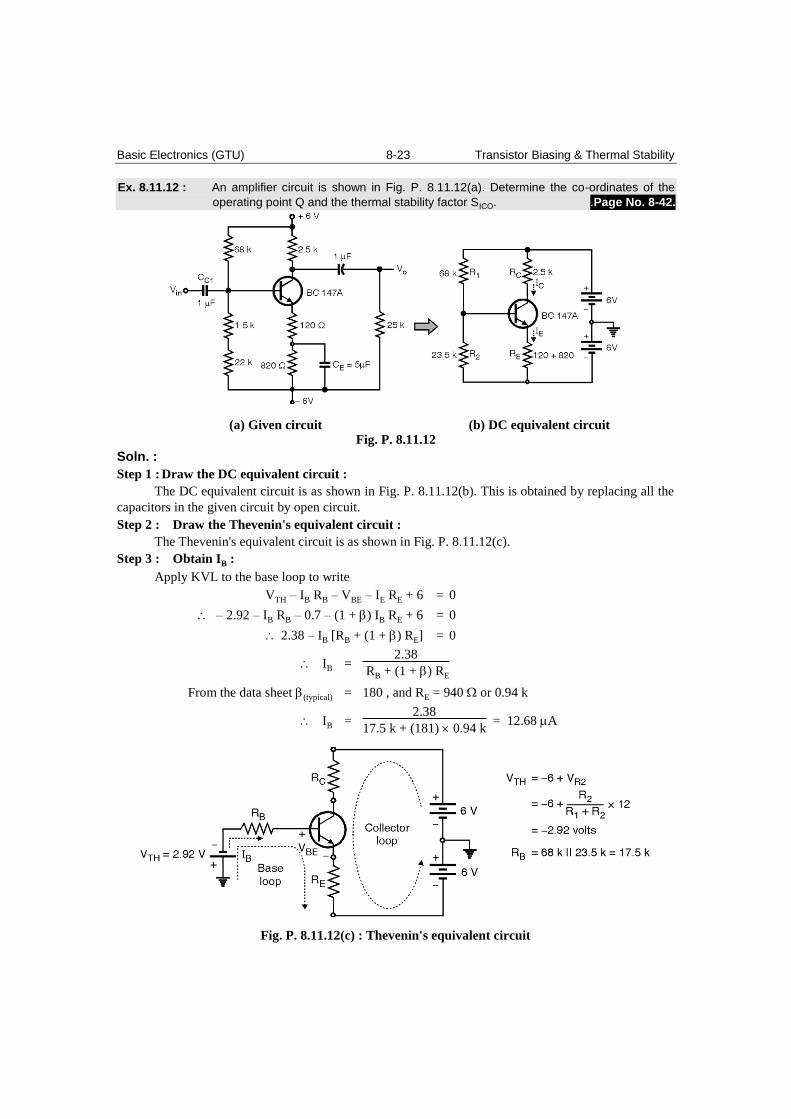
Ex. 8.11.12 : An amplifier circuit is shown in Fig. P. 8.11.12(a). Determine the co-ordinates of the
operating point Q and the thermal stability factor SICO. .Page No. 8-42.
(a) Given circuit (b) DC equivalent circuit Fig. P. 8.11.12
Soln. :
Step 1 : Draw the DC equivalent circuit :
The DC equivalent circuit is as shown in Fig. P. 8.11.12(b). This is obtained by replacing all the
capacitors in the given circuit by open circuit.
Step 2 : Draw the Thevenin's equivalent circuit :
The Thevenin's equivalent circuit is as shown in Fig. P. 8.11.12(c).
Step 3 : Obtain IB :
Apply KVL to the base loop to write
VTH – IB RB – VBE – IE RE + 6 = 0
– 2.92 – IB RB – 0.7 – (1 + ) IB RE + 6 = 0
2.38 – IB [RB + (1 + ) RE] = 0
IB = 2.38
RB + (1 + ) RE
From the data sheet (typical) = 180 , and RE = 940 or 0.94 k
IB = 2.38
17.5 k + (181) 0.94 k = 12.68 A
Fig. P. 8.11.12(c) : Thevenin's equivalent circuit

Basic Electronics (GTU) 8-24 Transistor Biasing & Thermal Stability
Step 4 : Calculate IC and VCE :
IC = IB = 180 12.68 10– 6
= 2.283 mA ...Ans.
IE = (1 + ) IB = 181 12.68 10– 6
= 2.2951 mA
Apply KVL to the collector loop to write
6 – IC RC – VCE – IE RE + 6 = 0
VCE = 12 – IC RC – IE RE = 12 – (2.283 2.5) – (2.2951 0.94)
VCE = 4.135 Volts ...Ans.
Step 5 : Calculate SICO :
For a voltage divider bias circuit SICO is given by,
SICO = IC
ICO
= (1 + ) 1 + (RB/ RE)
(1 + ) + (RB/ RE)
= (1 + 180) 1 + (17.5/0.94)
(1 + 180) + (17.5/0.94)
SICO = 17.79 ...Ans.
Ex. 8.11.13 : In the circuit of Fig. P. 8.11.13, transistor has = 100 and VBE (active) = 0.6 V. Calculate
the values of R1 and R3 such that collector current is of 1 mA and VCE = 2.5 V.
.Page No. 8-43.
Fig. P. 8.11.13 : Given circuit
Soln. :
1. To calculate value of R3 :
It is given that IC = 1 mA and VCE = 2.5 V.
Apply KVL to the collector circuit of Fig. P. 8.11.13 to get,
VCC = IC R3 + VCE + IE R4
Substitute IE = (IC + IB) and IB = IC /
VCC = IC R3 + 2.5 +
IC +
IC
R4
Substituting the other values, 5 = (1 10– 3
R3) + 2.5 +
1 mA +
1 mA
100 300
5 = (1 10– 3
R3) + 2.803
R3 = 2.197 k ...Ans.

Basic Electronics (GTU) 8-25 Transistor Biasing & Thermal Stability
2. To calculate the value of R1 :
R1 = VR1
I1
= 5 – VB
I2 + IB
But VB = IE R4 + VBE
But IE = 1.01 mA
VB = (1.01 0.3) + 0.6 = 0.903 volt
and IB = IC
=
1 mA
100 = 0.01 mA = 10A
As R2 = 10 k ...given
I2 = VB
R2
= 0.903
10 103 = 0.0903 10
– 3
I2 = 90.3 A
Substituting all these values we get,
R1 = 5 – 0.903
(90.3 + 10) 10– 6 = 40.8 k ...Ans.
Ex. 8.11.14 : The circuit shown in Fig. P. 8.11.14(a) uses a Si transistor with = 200 and it is designed
to make Vo = 0 and VCEQ = 3 V. (a) Determine RC and RE (b) Using the values obtained in
(a) find the change in Vo if is halved. .Page No. 8-43.
Fig. P. 8.11.14(a) : Given circuit
Soln. :
(a) Redraw the output circuit of the Fig. P. 8.11.14(a) :
Redraw only the output circuit of Fig. P. 8.11.14(a) as shown
in Fig P. 8.11.14(b). Now apply KVL to write,
6 – IC RC – VCEQ – IE RE + 6 = 0 ...(1)
But VCEQ = 3 V
12 – IC RC – 3 – IE RE = 0
9 – IC RC – IE RE = 0 ...(2)
Fig. P. 8.11.14(b)

Basic Electronics (GTU) 8-26 Transistor Biasing & Thermal Stability
Looking at Fig. P. 8.11.14(b) we can write that,
Vo = VCEQ + IE RE – 6 ...(3)
But Vo = 0 and VCEQ = 3 V
0 = 3 + IE RE – 6
IE RE = 3 V ...(4)
Substitute Equation (4) into Equation (2) to get,
9 – IC RC – 3 = 0
IC RC = 6 V ...(5)
We know that = 200 but we do not know the value of IB to calculate IC and IE.
1. To obtain the value of IB :
Redraw only the input side of the given circuit as shown in
Fig. P. 8.11.14(c).
Applying KVL we get,
0 – [(90 k || 90 k) IB] – 0.7 – IE RE + 6 = 0
Substitute IE RE = 3 V
And (90 || 90) = 45 k to get Fig. P. 8.11.14(c)
0 – (45 k IB) – 0.7 – 3 + 6 = 0
IB = 58.11 A ...(6)
2. To obtain the value of RE :
IE RE = 3 V
RE = 3
IE
= 3
(1 + ) IB
RE = 3
201 51.11 10– 6 = 292 ...Ans.
3. To obtain the value of RC :
IC RC = 6 V
RC = 6
IC
= 6
IB
= 6
200 51.11 10– 6 = 586.96 ...Ans.
(b) To obtain the change in Vo if = 100 :
The new values of IC and IE are as follows :
IC = 100 51.11 A = 5.11 mA
and IE = 101 51.11 A = 5.16 mA
From Equation (3) we have,
Vo = VCEQ + IE RE – 6 = 3 + (5.16 10– 3 292) – 6
Vo = – 1.4932 Volts
Hence change in Vo = – 1.4932 – 0 = – 1.4932 Volts ...Ans.