chapter2 msi logic circuit
DESCRIPTION
Logic circuit book chapter 2 onlyTRANSCRIPT

BKTP.HCM
2010dce
Chapter 2MSI LOGIC CIRCUITS
Faculty of Computer Science and EngineeringDepartment of Computer Engineering
©2010, CE Department

2010dce Outline
• Decoder• Encoder• Multiplexer• Demultiplexer• Magnitude Comparator• Code Converters• Tristate Register• Data Bus Operation
©2010, CE Department 2

2010dce
3©2010, CE Department
Decoder• Accept a set of inputs that represents a binary
number and activate only the output thatcorresponds to that input number
• May not utilize all of 2N possible input codes

2010dce
4©2010, CE Department
Decoder – Example• 3-line-to-8-line decoder– binary-to-octal decoder– 1-of-8 decoder

2010dce
5©2010, CE Department
Decoder – ENABLE inputs• Some decoders have one or more ENABLE
inputs to control the operation of the decoder• Example: 74138

2010dce
6©2010, CE Department
Decoder - Combination• Four 74ALS138s and an INVERTER can be
arranged to function as a 1-of-32 decoder

2010dce
7©2010, CE Department
BCD-to-Decimal Decoder (7442)• 4-to-10 decoder (1-of-10
decoder)– Activate one output that
corresponds to BCD input(0000 1001)
– Invalid inputs (1010 1111):none of outputs will beactivated

2010dce
8©2010, CE Department
BCD-to-Decimal Decoder/Driver• Open-collector outputs can operate at higher
current and voltage limits than a normal TTLoutputs
• Directly driving loads: LEDs, lamps, relays, dcmotors, ...
• Example: 7445 outputs can sink up to 80mA inLOW state

2010dce
9©2010, CE Department
Decoder Applications• Counter/Decoder combination used to provide
timing and sequencing operations

2010dce
10©2010, CE Department
7-Segment LED• Form the decimal characters 0 9, sometimes
the hex characters A F• Use light-emitting diodes (LEDs) for each
segment• Normal brightness: 10mA, 2.7V

2010dce
11©2010, CE Department
BCD-to-7-segment Decoder/Driver• 4-bit BCD input, each output is activated more
than one combination of inputs• Common-Anode, Common-Cathode LEDs

2010dce
12©2010, CE Department
Liquid-Crystal Displays• Control the reflection of available light
– Reflective LCD– Backlit LCD
• Very low power consumption, low-voltage (3 – 15V rms), low frequency (25 to 60Hz) ac signal,very little current
• Backplane is common to all segments• Ac voltage is applied between the segment and
the backplane to turn on this segment– Not reflect the incident light, they appear dark against
their background

2010dce Driving an LCD (1)
• In practice, produce the required ac voltage byapplying out-of-phase square waves to thesegment and the backplane
©2010, CE Department 13

2010dce Driving an LCD (2)
• Use CMOS 74HC4511BCD-to-7-segmentdecoder/driver
• 74HC4543: decoder/driverand XOR gate areavailable on a single chip
• CMOS device are used todrive LCD:– Less power than TTL– LOW-state is almost exactly
0V
©2010, CE Department 14

2010dce Encoder
• The opposite of decoding process• Encoder has a number of input lines, only one of
which is activated at a given time, and producesa N-bit output code
©2010, CE Department 15

2010dce Encoder - Example
• Octal-to-binary encoder (8-line-to-3-line encoder)– Accept 8 inputs lines and produce a 3-bit output code
©2010, CE Department 16

2010dce Priority Encoder
• When more than one input is activated at onetime, the output code will respond to the highest-numbered input (74148)– Example: A6, A2, A0 are activated output code is
110 (6)• 74147 Decimal-to-BCD Priority Encoder
©2010, CE Department 17

2010dce Switch Encoder
• Data input must bemanually entered intoa digital system– 12 D-FF: three 4-bit
FF registers– JK-FF: control the
transfer of data to theappropriate register
– T-FF: One-shot
©2010, CE Department 18

2010dce Multiplexers (MUX - Data Selectors)
• Accept several digital data inputs and select oneof them at any given time to pass on to the output
• The routing of the desired data input to the outputis controlled by SELECT inputs
©2010, CE Department 19

2010dce Basic Two-Input Multiplexer
• Boolean expression for the outputZ = I0S’ + I1S
− S = 0: Z = I0.1 + I1.0 = I0 (gate 2 enabled)− S = 1: Z = I0.0 + I1.1 = I1 (gate 1 enabled)
©2010, CE Department 20

2010dce
• Four-Input Multiplexer
Other Multiplexer (1)
©2010, CE Department 21

2010dce Other Multiplexer (2)
©2010, CE Department 22
• Eight-Input Multiplexer• 16-Input Multiplexer

2010dce Other Multiplexer (3)
• Quad Two-Input MUX (74157)
©2010, CE Department 23

2010dce Multiplexer Application (1)
• Data routing: routedata from one ofseveral sources toone destination– SELECT = 1: Counter1– SELECT = 0: Counter2
• Purpose: time-share thedecoder/drivers anddisplay circuits betweenseveral counters
©2010, CE Department 24

2010dce Multiplexer Application (2)
• Parallel-to-serialconversion– 3-bit (MOD-8) counter
is used to provide the select code bits S2S1S0
©2010, CE Department 25
X7X6X5X4X3X2X1X0 = 10110101

2010dce Multiplexer Application (3)
• Operation sequencing: in a control sequencer
©2010, CE Department 26

2010dce Multiplexer Application (4)
©2010, CE Department 27
• Logic-function generation: multiplexer can beused to implement logic functions directly from atruth table without the need for simplification– Select inputs: logic variables– Data inputs: connected to permanently HIGH or LOW
to satisfy the truth table

2010dce Demultiplexers (Data Distributors)
• Performs the reverse operations with multiplexer• Take single input and distribute it over several
outputs• Like a multiposition switch
©2010, CE Department 28

2010dce 1-Line-to-8-Line Demultiplexer
©2010, CE Department 29
I: Data input

2010dce 1-Line-to-8-Line Demultiplexer
• Compare to decoder– Decoder that have an ENABLE input can be used as a
demultiplexer decoder/demultiplexer• Binary code inputs serving as the SELECT inputs• ENABLE input serving as the data input I
©2010, CE Department 30

2010dce
• Clock Demultiplexer: Clock signal is routed tothe desired destination under control of theSELECT lines
Demultiplexer Application (1)
©2010, CE Department 31

2010dce Demultiplexer Application (2)
• Security Monitoring System: open/close statusof many access doors is to be monitored.– Each door controls state of a switch– To reduce the amount of wiring to the monitoring
panel use a multiplexer/demultiplexer combination– State of each switch is displayed on LEDs
©2010, CE Department 32

2010dce
©2010, CE Department 33
Security monitoring system

2010dce Demultiplexer Application (3)
• Synchronous Data Transmission System– Used to serially transmit M n-bit data words from a
transmitter to a remote receiver– LSB of each register is connected as a data input to
the M-input multiplexer• The data are said to be time-division-multiplexed
– Receiver: contains a 1-to-M demultiplexer
©2010, CE Department 34

2010dce
©2010, CE Department 35
Synchronous data transmission system

2010dce
©2010, CE Department 36
Waveforms during one complete transmission cycle

2010dce Magnitude Comparator
• Compare two input binary quantities andgenerate outputs to indicate which one has thegreater magnitude
• 74HC85– Data inputs: two unsigned 4-bit binary numbers– Outputs: 3 active-HIGH outputs (OA>B, OA<B, OA=B)
©2010, CE Department 37

2010dce Magnitude Comparator
©2010, CE Department 38

2010dce Magnitude Comparator
• Cascading Inputs– Provide a means for expanding the comparison
operation to more than 4 bits by cascading 2 or more4-bit comparators
©2010, CE Department 39

2010dce Magnitude Comparator - Application
©2010, CE Department 40
Magnitude comparator used in a digital thermostat

2010dce Code Converters
• Change data presented in one type of binarycode to another type of binary code– BCD-to-7-segment decoder/driver is a code converter– Some of the more common code conversion
• BCD to 7-segment• BCD to binary• Binary to BCD• Binary to Gray code• Gray code to binary• ASCII to EBCDIC• EBCDIC to ASCII
(EBCDIC is an alphanumeric code developed by IBM similar to ASCII)©2010, CE Department 41

2010dce BCD-to-Binary Converter
• Basic idea– Inputs to the converter are the two 4-bit code groups
of the decimal value• D0C0B0A0: represent the 100 or units digit• D1C1B1A1: represent the 101 or tens digit
– Outputs: b6b5b4b3b2b1b0 – 7 bits of the binaryequivalent of the same decimal value
©2010, CE Department 42

2010dce BCD-to-Binary Converter
• BCD-to-binary converter can be accomplishedwith either hardware of software– Hardware method: generally faster but require extra
circuit– Software method: no extra circuit but take more time
(step by step)– The method chosen in a particular application
depends on whether or not conversion time is animportant consideration
©2010, CE Department 43

2010dce BCD-to-Binary Converter
• Conversion Process– The bits have decimal weights which are 8, 4, 2, 1 but
differ by a factor of 10 from one code group to the next– Decimal weight of each bit can be converted to its
binary equivalent– Compute the binary sum of the binary equivalents of all bits
in the BCD representation that are 1s
©2010, CE Department 44

2010dce BCD-to-Binary Converter
• Example: Covert 01010010 (52BCD) to binary
©2010, CE Department 45

2010dce BCD-to-Binary Converter
• Circuit Implementation: use binary adder circuits– A0: directly to b0– B0, A1 contribute to b1, ...
©2010, CE Department 46

2010dce Data Busing
• Data bus: a common set of connecting lines forthe transfer of data
• Many different devices can have their outputsand inputs tied to the common data bus lines
• Devices tied to the data bus will often havetristate outputs or tied to the data bus throughtristate buffers
• Some of the devices that are commonlyconnected to a data bus:– Microprocessor, semiconductor memory chips, Digital-
to-analog/Analog-to-digital converters (DACs/ADCs)
©2010, CE Department 47

2010dce
©2010, CE Department 48
Three different devices are connected to data bus
Only one device at a time is enabled to avoid bus
contention

2010dce 74ALS173/HC173 Tristate Register
• Tristate Register allow outputs of devices to betied to a data bus
©2010, CE Department 49

2010dce
©2010, CE Department 50
Logic Diagram for the 74ALS173 tristate register

2010dce Data bus Operation
• Example: Register –register data transfer– Each register has its
pair of OE inputs and IEinputs tied together
– Data bus: DB0 – DB3
– 3 registers have theirinputs and outputsconnected together
– Only one register haveits output enabled, other2 registers outputsremain in Hi-Z state
©2010, CE Department 51

2010dce Data bus Operation
• Data Transfer Operation– The control unit will generate the signals that select
which register will put its data on the data bus andwhich one will take the data from the data bus
– Example:• t1: only register A have its output enabled
OEA = 0 OEB = OEC = 1• t2: only register C should have its inputs enabled
IEC = 0 IEA = IEB = 1
©2010, CE Department 52
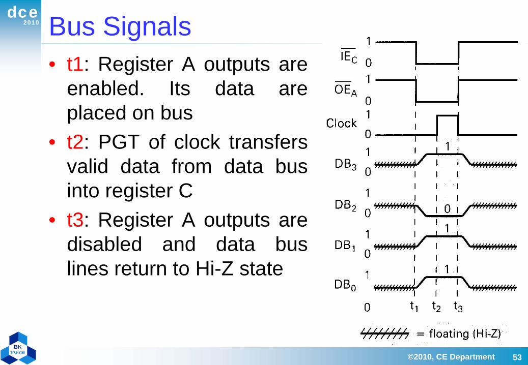
2010dce Bus Signals
• t1: Register A outputs areenabled. Its data areplaced on bus
• t2: PGT of clock transfersvalid data from data businto register C
• t3: Register A outputs aredisabled and data buslines return to Hi-Z state
©2010, CE Department 53

2010dce Simplified Bus Timing Diagram
• Use only a single timing waveform to representthe complete set of bus lines
©2010, CE Department 54

2010dce Expanding the Bus
• The number of lines on the data bus will dependon the size of the data word (unit of data) that isto be transferred over the bus– Example: 8-bit word size 8-line data bus
• Some devices will need to be connected to thebus through a bus driver
• Bus driver– Tristate outputs with a very low output impedance
rapidly charge and discharge the bus capacitance– Reduce transition time of signal
©2010, CE Department 55

2010dce Expanding the Bus
©2010, CE Department 56
74HC541 octal bus driver

2010dce Simplified Bus Representation (1)
• Use on block diagramand in some circuitschematics
• The connections to andfrom the data bus arerepresented by widearrows
• The numbers in brackets([ ]) indicate the numberof bits of register andnumber of lines of databus
©2010, CE Department 57

2010dce Simplified Bus Representation (2)
• Bundle method– A single line denotes the data bus– “/8” denotes an eight-line data bus
©2010, CE Department 58

2010dce Bidirectional Busing
• Some devices have both inputs and outputsconnected to the data bus– Inputs and outputs are connected together internal to
the chip• Reduce the number of IC pins• Reduce number of connections to the bus
– Input lines (I0/D0 to I3/D3) and output lines (O0 to O3)have been replaced by input/output lines (I/O0 to I/O3)
– I/O line will function as either an input or an outputdepending on the state of the enable inputs
Bidirectional data lines
©2010, CE Department 59

2010dce Bidirectional Busing
©2010, CE Department 60
Bidirectional register connected to data bus

2010dce
61
Reference• Chapter 9, Digital System – Principles and
Applications, Ronald J.Tocci, Neal S. Widmer