city university of hong kong department of physics...
TRANSCRIPT

CITY UNIVERSITY OF HONG KONG
DEPARTMENT OF
PHYSICS AND MATERIALS SCIENCE
BACHELOR OF ENGINEERING (HONS) IN MATERIALS ENGINEERING
2008-2009
DISSERTATION
Arrays of ZnO nanowires for photovoltaic devices
by
WANG Yunqi
March 2009

Arrays of ZnO nanowires for photovoltaic devices
By
WANG Yunqi
Submitted in partial fulfilment of the
requirements for the degree of
BACHELOR OF ENGINEERING (HONS)
IN
MATERIALS ENGINEERING
from
City University of Hong Kong
March 2009
Project Supervisor : Prof. Igor Bello

i
Acknowledgement
Despite a short period of seven months, the project has been the most invaluable and
constructive experience in my starting scientific career. The final year project provides me an
opportunity to carry out research work independently and systematically. From designing
experiments to analyzing results and drawing conclusions, I have gained precious research
experience and realized the importance of applying scientific knowledge into practice. Here, I
write to extend my heartfelt thanks to those who have assisted me to complete this
dissertation.
Firstly, I would like to express my sincere gratitude to my project supervisor, Prof. Igor Bello,
for his continuous support and encouragement throughout the entire work. Prof. Bello is not
only my mentor but also my friend. He was always there to meet and give invaluable advices,
to raise thoughtful questions, and to proofread and mark up my dissertation. Secondly, I
would like to thank my assessor, Dr. C H Shek, who talked and discussed with me on the
progress of the project and encountered problems. Also, I wish to thank the research student
Mr. Chen Zhenhua who assisted me in experiment designs and trained me in various
characterization techniques. He always shared his ideas and gave me constructive
suggestions.

ii
Table of Contents
Acknowledgement i
Table of Contents ii
List of Figures v
List of Tables viii
Abstract ix
Page
1 Introduction and Objectives 1
2 Literature Review 3
2.1 Nanotechnology 3
2.2 Nanowires 4
2.3 Synthesis of One-dimensional (1D) Semiconductor Nanomaterials 4
2.3.1 Vapor-Liquid-Solid (VLS) Mechanism 4
2.3.2 Solution-Liquid-Solid (SLS) Mechanism 5
2.3.3 Vapor-Solid (VS) Mechanism 5
2.3.4 Oxide-Assisted Growth (OAG) Mechanism 6
2.3.5 Other Growth Mechanisms 7
2.4 Synthesis of Heterostructures 7
2.4.1 Axial Nano-heterostructures 7
2.4.2 Radial Nano-heterostructures 8
2.4.3 Branched Nano-heterostructures 9
2.5 Zinc Oxide nanowires 9
2.5.1 General Properties of Zinc Oxide 9
2.5.2 Growth of Aligned ZnO Nanowires 10
2.5.3 Application of Zinc Oxide in Solar Cells 11
3 Experimental Procedures 13
3.1 Fabrication of ZnO Nanowire Arrays 13
3.1.1 Synthesis of ZnO Nanowire Arrays by a Solution Method 13
3.1.1.1 Cleaning the Substrates 13

iii
3.1.1.2 ZnO Seeding and Nanowire Growth 13
3.1.2 Synthesis of ZnO Nanowire Arrays by a Thermal Evaporation Method 14
3.1.2.1 Preparation of Aluminum Doped Zinc Oxide Buffer Layer 14
3.1.2.2 Growth of ZnO Nanowire Arrays on AZO/Si Substrates 14
3.2 Design and Fabrication of Photovoltaic Devices 15
3.2.1 Fabrication of Dye Sensitized Solar Cells (DSSCs) 15
3.2.1.1 Adsorption of Dye 15
3.2.1.2 Fabrication of Solar Cells 16
3.2.2 Fabrication of Hybrid Dye Sensitized Solar Cells 16
3.2.2.1 Coating Platinum Films on the Counter Electrodes 16
3.2.2.2 Deposition of Silver Pad on the Bottom Electrode 17
3.2.2.3 Attachment of Gold Nanoparticles to ZnO Nanowire Arrays 18
3.2.2.4 Adsorption of Dye and Construction of Hybrid Dye Sensitized
Solar Cells 18
4 Results and Discussions 19
4.1 Characterization of Synthesized ZnO Nanowire Arrays 19
4.1.1 Morphological and Topographic Features of the Prepared ZnO Nanowire
Arrays 19
4.1.2 The Structure of Synthesized Nanowires on Nanometer and Atomic Scales 20
4.1.3 Structural Analysis of ZnO Nanowires by X-ray Diffraction 21
4.1.4 Photoluminescence (PL) Induced in Prepared ZnO Nanowires 23
4.2 Characterization of ZnO Nanowire-based Solar Cells 24
4.2.1 Characterization of Conventional Dye Sensitized Solar Cells 24
4.2.1.1 The Effect of Dye Coating on the Light Absorption 24
4.2.1.2 Current density–Voltage (J-V) Characteristics of Dye Sensitized
Solar Cells 25
4.2.1.3 Effect of the Light Intensity on the Solar Cell Performance 28
4.2.2 Dye Free Schottky Barrier Solar Cells 29
4.2.2.1 Analysis of Distribution of Gold Nanoparticles 29
4.2.2.2 Analysis of Current Density–Voltage (J-V) Characteristics of Dye
Free Schottky Barrier Solar Cells 30
4.2.2.3 Performance of Dye Free Solar Cells with Schottky interfaces
under Different Light Intensities 32
4.2.3 Characterization of Hybrid Dye Sensitized Solar Cells 33

iv
4.2.3.1 Performance of Designed Hybrid Dye Sensitized Solar Cells 33
4.2.3.2 The Effect of the Characteristics of Gold Coatings on the
Hybrid Solar Cell Performance 35
5 Conclusions 36
6 References 37

v
List of Figures
Page
Fig.2-1 Growth of a silicon nanowire by VLS. (a) Initial condition with a
liquid droplet on a substrate. (b) Growing nanowire with a liquid
droplet at the top tip of a nanowire.
5
Fig. 2-2 A schematic diagram contrasting the OAG method and VLS growth
method of nanowires.
6
Fig. 2-3 Synthesis of nanowire heterostructures. (a) First reactant material leads
to 1D axial growth. (b) A change in the reactant leads to either (c) axial
heterostructure growth or (d) radial heterostructure growth. Alternating
reactants will produce (e) axial superlattices or (f) core-multi-shell
structures.
8
Fig. 2-4 Branched nano-heterostructures. The colors indicate regions with
distinct chemical composition and/or doping.
9
Fig. 2-5 Crystal structure of ZnO.
10
Fig. 2-6 Schematic diagram of a dye sensitized solar cell, based on ZnO
nanowire arrays.
11
Fig. 3-1 Schematic diagram of the furnace with a horizontal double-tube
configuration.
15
Fig. 3-2 Schematic diagram of the constructed solar cell. Light enters the
cell through the bottom electrode.
16
Fig. 3-3 Schematic diagram of the electrochemical deposition setup.
17
Fig. 3-4 Thermal evaporation system used in deposition of silver pads on the
base electrodes.
17
Fig. 3-5 Schematic diagram of the constructed hybrid solar cell. Light enters
the cell via the bottom transparent electrode.
18
Fig. 4-1 SEM micrographs of synthesized ZnO nanowires prepared on ITO
buffer layers at 90 o
C by a solution method: (a) Cross-sectional
19

vi
image; (b) Magnified image shows faceted nanowire structures
indicating the single crystalline nature of individual nanowire.
Fig. 4-2 SEM micrograph depicts synthesized ZnO nanowires prepared on
an AZO buffer layer at 700 oC by thermal evaporation.
19
Fig. 4-3 TEM micrograph of ZnO nanowires: (a) Conventional TEM bright
field image of a single ZnO nanowire with a hemispherical tip; (b)
high-resolution TEM (HRTEM) image of a typical ZnO nanowire
showing its c-axial growth direction. The inset shows the
corresponding selected area electron diffraction (SAED).
21
Fig. 4-4(a) XRD pattern of ZnO nanowire arrays synthesized by solution
method.
21
Fig. 4-4(b) XRD pattern of ZnO nanowire arrays synthesized on AZO film by a
thermal evaporation method.
22
Fig. 4-5(a) Room temperature PL spectrum collected from the ZnO nanowire
arrays prepared by a solution method.
23
Fig. 4-5(b) Room temperature PL spectrum acquired from the ZnO nanowire
arrays prepared by a thermal evaporation method.
23
Fig. 4-6 Band structure: the levels of defects in ZnO.
24
Fig. 4-7 UV-Vis absorption spectra of as-grown and dye-coated ZnO
nanowire arrays.
24
Fig. 4-8(a) TEM image of dye-coated ZnO nanowires. The inset shows a single
ZnO nanowire without coating dye.
25
Fig. 4-8(b) Schematic illustration of exciton dissociation at the ZnO/dye
interface and electron injection into the conduction band of ZnO.
25
Fig. 4-9 Schematic band diagram describing the charge transfer processes
involved in DSSC.
26
Fig. 4-10 (a) J-V curves for the solar cell in the dark and under simulated
AM1.5G illumination with intensity of 100 mW/cm². (b)
Corresponding schematic photovoltaic device structure.
27
vii
Fig. 4-11 (a) J-V characteristics of the solar cell with the contact treatment in
dark and under simulated AM1.5G illumination with intensity of
100 mW/cm². (b) Corresponding schematic photovoltaic device
structure.
28
Fig. 4-12 J-V characteristics of the contact treated solar cell under
illumination with intensities of 80, 100 and 120 mW/cm².
28
Fig. 4-13 (a) SEM image of ZnO nanowires loaded with Au nanoparticles; (b)
bright field TEM image of abstracted ZnO nanowires; (c) EDX
spectrum acquired from ZnO nanowires coated with Au
nanoparticles.
29
Fig. 4-14 J-V characteristics of the photovoltaic device with bare ZnO
nanowires and the device with Au-coated ZnO nanowires. The
characteristics were obtained under simulated AM1.5G illumination
with intensity of 100 mW/cm².
31
Fig. 4-15 UV-Vis absorption spectra collected from bare and Au coated ZnO
nanowires.
31
Fig. 4-16 Schematic band diagram describing the charge transfer processes
involved in the dye free Schottky barrier solar cell.
32
Fig. 4-17 Performance of dye free Schottky barrier solar cells under light
illumination with intensities of 40, 60 and 80 mW/cm².
32
Fig. 4-18 (a) Typical J-V characteristics of the hybrid solar cell referenced to
that based on bare ZnO nanowires measured under simulated
AM1.5G illumination with intensity of 100 mW/cm². (b) The
corresponding schematic of hybrid solar cell structure.
33
Fig. 4-19 Energy level diagram and mechanism of photocurrent generation in
the hybrid DSSC. C.B. and V.B. are the conduction and valence
bands of ZnO, respectively.
34
Fig. 4-20 J-V characteristics of the solar cells constructed with bare ZnO
nanowires, and ZnO nanowires coated thick Au layer and thin layer
35

viii
of Au nanoparticles under simulated AM1.5G illumination with
intensity of 100 mW/cm².
List of Tables
Page
Table 4-1 Performance of the contact treated solar cell under different
illumination intensities.
29
Table 4-2 Parameters of dye free solar cells illuminated with different light
intensities.
32

ix
Abstract
The photovoltaic cells, also called solar cells, are electronic devices operated on principle of
conversion of solar energy to electricity. These novel sources of energy becomes more
increasingly important because firstly traditional fossil recourses will be exhausted for
several decades, and secondly the conversion of solar energy to electricity do not produce
environmentally unfriendly emission and represent unlimited source of energy. Therefore this
work focuses on design, fabrication and study solar cells. The solar cells are based on zinc
oxide nanowires with different devices architectures.
Zinc oxide (ZnO) nanowire arrays were synthesized directly on electrically conducting and
optically transparent indium tin oxide (ITO) films using solution and thermal evaporation
methods. The ITO films were deposited on glass substrates. ZnO nanowires have been grown
on the ITO in hydrothermal environment at 90 °C. Alternatively ZnO nanowires have also
been grown on aluminum doped zinc oxide (AZO) buffer layers prepared on silicon (Si)
substrates by thermal evaporation at 700 °C using a double-tube furnace system.
Different characterization techniques were employed to investigate the properties of
fabricated ZnO nanowires, which demonstrated that the ZnO nanowires synthesized by
thermal evaporation method show higher degree of the vertical alignment on the substrates,
and they comprise lower crystal defect densities. However, the low temperature environment
of solution method which can induce less damage to the electrical property of the bottom
electrode is more favorable to synthesize ZnO nanowire arrays used for constructing dye
sensitized solar cells (DSSCs).
Conventional DSSCs were designed and fabricated with using N719 dyed ZnO nanowire
arrays and iodine based redox electrolyte. After coating platinum thin films on the counter
electrodes, silver contact pads were deposited. The pads were used to bond wire leading for
external electronic circuit to determine the device parameters and overall performance. The
fill factor (FF) and energy conversion efficiency (η) of the DSSCs were improved from 0.28
to 0.36 and from 0.48 to 0.69 %, respectively, due to reducing photoelectron recombination at
the contact interfaces. The performance investigation of the fabricated DSSCs under different
illumination intensities indicated raising the power conversion efficiency η from 0.34 to
0.85 % as the intensity increased from 80 to 120 mW/cm².

x
Gold (Au) nanoparticles coated ZnO nanowire arrays have been employed to fabricate dye
free Schottky barrier solar cells. The Au nanoparticles enhanced the optical absorption of
ZnO nanowires in the visible light region due to their surface plasmon resonance. Upon
illumination, the photoelectrons generated within the plasmon excited Au nanoparticles were
injected into the conduction band of ZnO, and the electron donors (such as I -) from the
electrolyte would compensate the loss of electrons in Au nanoparticle surfaces,
simultaneously. The fill factor FF of the fabricated dye free Schottky barrier solar cell
reached about 0.5.
Hybrid DSSCs have also been designed and fabricated using ZnO nanowires coated Au
nanoparticles and applied ruthenium dye (N719) and redox electrolyte. Compared with
DSSCs with bare ZnO nanowires, the open circuit voltage (VOC) was improved from 0.51 to
0.64 V due to blocking effect of the Schottky barrier formed at ZnO/Au interface. As a result,
electron density increased at ZnO conduction band. The reduction of the short circuit current
density (JSC) can probably be ascribed to the increased surface defects of ZnO nanowires after
coating Au nanoparticles, and poor electron injection efficiency implying unsuitable bindings
of ZnO and dye molecules. Controlling the characteristics of Au nanoparticles coatings is
proposed to be vital for fabrication of hybrid DSSCs with enhanced performance.

1
1 Introduction and Objectives
Dye sensitized solar cells (DSSCs) are considered as one of the most promising photovoltaic
device architectures. Their potentially high solar-to-electrical power conversion efficiency
and a low fabrication cost make them very attractive for producing electricity in large scales
[1-3]. In some aspects, they are superior to traditional silicon solid-state solar cells based on
the p-n junction diodes. Instead of acting as the source of photoelectrons and provide electric
field to separate electrical charges, the semiconductor in DSSCs provides the path for
electron transport and the photoelectrons are generated by a photosensitive dye. The
interfaces between the electrolyte, semiconductor and dye play an important role in charge
separation.
It was reported that the solar energy conversion efficiency of DSSCs can achieve 11% by
using a titanium dioxide (TiO2) nanoparticle film as the photoanode [4]. Ruthenium
complexes and porous TiO2 structures have been mostly used as sensitizers and
semiconductor materials in DSSCs, respectively [5]. Although TiO2 nanoparticle films have
sufficiently large surface area for dye adsorption, they limit the device efficiency by
enhancing electron recombination probability and slowing electron transport rate which
essentially depends on the process of electrons diffusion to the anode through particles.
Consequently, vertical single crystalline nanowires which can provide a direct path to anode
are anticipated to replace nanoparticle films for further increasing the electron diffusion rate.
Over recent years, it was shown that Zinc oxide (ZnO), because of its suitable electronic and
optical properties, is one of the materials that could be incorporated into construction of in
DSSCs to improve their performance. ZnO has comparable band gap (3.37 eV) to TiO2,
much higher room temperature mobility (ZnO: 115-155 cm2V
-1s
-1, TiO2: < 10
-5 cm
2V
-1s
-1), a
high binding energy (60 meV), high breakdown strength, cohesion, and exaction stability. It
is also one of the hardest materials in the family of II–VI semiconductors. Various ZnO
nanostructures, comprising arrays of nanorods and nanowires, can be prepared on optically
transparent and electrically conducting oxide substrates using various methods. The surfaces
of these ZnO nanowires can be functionalized. It was reported that the arrays of highly
ordered ZnO nanowires in DSSCs design could provide a more open structures for filling

2
with hole-transporting materials [6-8]. The conversion efficiencies of the ZnO nanowire
based DSSCs are about 1.5% up to now.
Obviously in further development of ZnO DSSCs, the principal goals are to increase their
energy conversion efficiency. Primarily, the higher conversion efficiency can be provided by
spectral absorbance over a broader light range covering the visible and near-IR regions.
Particularly, modifying dyes can not only assist to higher absorbance but also to increase of
the open-circuit voltage which is influenced by the metal oxide electronegativity and the dye
ionization potential. The development of conversion efficiency also focuses on increasing of
the electron diffusion length and improvement of electron transport.
In this project, the main objectives are to synthesize ZnO nanowire arrays directly on
electrically conducting electrodes and design of photovoltaic structures that will lead to
higher conversion efficiencies. In the fundamental technological step, different
characterization techniques were employed to investigate the morphology, crystal structures,
optical and electrical properties of fabricated ZnO nanowires. DSSCs were built based on
dense arrays of ZnO nanowires. The efficiency of ZnO nanowires based DSSCs was further
improved via charge transport in the DSSCs. The counter electrode was coated with platinum
to enhance the hole transport as well as improving the catalyst behaviors of redox reaction in
electrolyte. A silver pad used for leading out wires was also deposited on the bottom
electrode and thermally treated to reduce the contact barrier. A hybrid structure of DSSCs,
ZnO nanowires coated with gold (Au) nanoparticles, was designed and constructed to
improve the light absorbance in visible range. Without involving dye, a Schottky barrier solar
cell based on Au nanoparticles coated ZnO nanowirs was also characterized and its working
principle was investigated in this project.

3
2 Literature review
2.1 Nanotechnology
Nanotechnology refers to a field of applied science which deals with matters on an atomic
and molecule scale and involves developing devices within that size [9]. Nanostructures
which correspond to the structures having at least one physical dimension between 1 to 100
nm have been constantly gaining interests for their peculiar and fascinating properties [10].
Recently, there are various nanostructures being under research, like carbon nanotubes,
nanowires [11], nanobelts, nanopropellers, nanosprings, nanorings, nanobows, nanorods [12].
It has been reported that various techniques can be used to synthesize one dimensional
nanostructures, for example, chemical vapor deposition, physical vapor deposition (PVD),
laser ablation, hydrothermal [14].
The synthesized nanomaterials are extremely useful in both present and future semiconductor
industry. Recently, electronic devices are being made in smaller and smaller sizes and of
better performance. However, traditional top-down approaches, refer to assembling small
scale devices from large ones directly [15], like etching and lithographic, are facing the
problem of a near-exponential increase in cost associated with each new level improvement
for manufacture. On the contrary, bottom-up approaches, which correspond to arranging
nano-objects with well defined chemical or physical properties into more complex
components, have been applied to alternate the conventional top-down methods. It is much
like the way nature constructs complex biological systems using proteins and other
macromolecules [16].
Lieber suggested three key areas that enable bottom-up approaches for nanotechnology. First,
by rational design and predictable synthesis, chemical properties and the corresponding
physical properties of nanoscale building blocks need to be preciously controlled. Second, the
limits of functional devices based on these building blocks should be developed and explored
critically. Third, hierarchical assembly methods that can organize building blocks into the
architectures which enable high density of integration with predictable function should be
developed [16].

4
2.2 Nanowires
Since late 1990s, the field of semiconductor nanowires has been gaining interest among
science and engineering communities. High carrier mobility and large surface area are two
main priorities of nanowires. As a result, nanowires have various applications including high
performance field effect transistors (FETs), dye sensitized solar cells [17], chemical sensors
[18, 19] and ultrasensitive bio-sensors [20, 21]. Besides, nanowire-based on-chip photonic
devices, including light-emitting diodes [22], lasers [23–26], active waveguides [27, 28] and
integrated electro-optic modulators, have been explored as well for the optical cavity and
waveguide properties of semiconductor nanowires.
2.3 Synthesis of One-dimensional (1D) Semiconductor Nanomaterials
The rational design and synthesis of nanoscale materials are critical to work directed towards
understanding fundamental properties, creating nanostructured materials, and developing
nanotechnology [46]. Wagner and Ellis first investigated the catalyst-assisted chemical vapor
deposition (CVD) for growing single silicon crystal in 1964 [46]. Among the numerous
methods that have been developed to design and rationally synthesize nanowires with
predictable control over the key structural, chemical, and physical properties, the strategy that
involves exploiting a “catalyst” to confine growth in 1D has received increasing focus in the
past several years [16].
Classified by the different phases involved in the reaction, this strategy is cataloged into
vapor–liquid–solid (VLS) [13], solution–liquid–solid (SLS) [30], and vapor–solid (VS)
growth [36].
2.3.1 Vapor-Liquid-Solid (VLS) Mechanism
The VLS growth mechanism was first proposed by Wagner and Ellis to explain the
unidirectional silicon single crystal growth [29]. In VLS growth, a nanometer-scale catalyst
particle which can form a liquid solution with the nanowire material is involved. The size of
the initial nucleation event and the nanowire diameter are determined by the catalyst particle
size. The crystalline nanowire can be nucleated when the liquid solution, a nanoscale droplet,
becomes supersaturated. Then, by adding reactant selectively to this nanoscale droplet, the
nanowire can be grown [13]. The orientation of the nanowire is determined by the surface

5
lattice of the substrate on which an epitaxial relationship can be built [16]. Fig. 2-1 illustrates
the growth of a silicon crystal by VLS.
An important feature of this approach to nanowire growth is that phase diagrams can be used
to select catalyst, composition of catalyst and nanowire material, and temperature for
successful growth for different nanowire materials. Having this general idea, it is possible to
grow nanowire with all of the periodic table’s main group elemental, binary, and related alloy
semiconductors in a controlled fashion essentially. This general approach also enables control
of nanowire diameter and length [13].
2.3.2 Solution-Liquid-Solid (SLS) Mechanism
The Solution-Liquid-Solid mechanism is quite similar to VLS mechanism. The difference is
that the solution phase in the SLS reaction takes place of the vapor phase in the reaction of
VLS mechanism. This strategy has been reported to synthesize InP, InAs and GaAs
nanowires [30], and AlxGa1- x As nanowhiskers [31]. Buhro’s research group reported that
they found the diameter of a GaAs nanowire was smaller than the diameter of the catalyst
nanoparticle from which it grew [30]. This contrasts with the results of VLS growth which
shows the diameter of the nanowires being similar or greater than the initial diameters of the
catalyst nanoparticles [32-35]. They concluded the difference was due to the high reaction
temperature of VLS (≥500 oC), which increases the size of the catalyst nanoparticle prior to
nanowire growth. On the contrary, smaller nanowire diameters can be achieved by the
low-temperature (203 oC) SLS method [30].
2.3.3 Vapor-Solid (VS) Mechanism
Unlike VLS and SLS mechanism, there is no additional metal employed as the catalyst in
vapor-solid (VS) process. Vapors of a material for the nanowire growth are produced by
(b) (a)
Fig.2-1 Growth of a silicon nanowire by
VLS. (a) Initial condition with a liquid
droplet on a substrate. (b) Growing
nanowire with liquid droplet at the top tip of
a nanowire [46].

6
thermal evaporation at high temperature. As carried by the inert gas (e.g. N2, Ar) to the
downstream regions of lower temperature, the vapors begin to condense on the substrate
surface and crystallize. A competition in growth rate among different crystallographic
directions starts at the initial stage of crystallization. Once the condition of a favored
anisotropic one-dimensional growth occurs, the nanowire material atoms will strike on the
specific favorable advancing plane to invoke and continue the one-dimensional growth and
hence forming nanowires [36]. For the vapor-solid (VS) mechanism, the supersaturation ratio
of the condensing species in the gas is critical to the formation of one-dimensional
nanostructures. The supersaturation ratio of the condensing species must be below some
critical value for anisotropic growth, while, a medium supersaturation ratio results in bulk
crystals. For high supersaturation ratios, homogeneous nucleation in vapor phases leads to
powder formation [36].
2.3.4 Oxide-Assisted Growth (OAG) Mechanism
Oxide-assisted growth (OAG) method was developed by Lee’s group in 1998 [37]. This
method can produce large quantities of silicon nanowires without the need of a metal catalyst,
which hence yields high-purity nanowires that are free of metal impurities [37, 38-41].
The comparison between OAG method and VLS growth method are demonstrated in Fig.
2-2. The mechanism of the Si nanowires growth was explained by Lee’s group. First, the
deposited silicon sub-oxide cluster can be fixed on the substrate because of the strong bonds
between some of the reacted silicon atoms and substrate atoms. Non-bonded reactive silicon
atoms in the same cluster provide their dangling bonds directed outward from the surface as
nuclei to absorb additional reactive silicon oxide cluster and facilitate the formation of Si
nanowires. The growth of the silicon domain after nucleation may be crystallographically
Fig. 2-2 A schematic diagram
contrasting the OAG and VLS
growth methods of nanowires
[42].

7
dependent subsequently [42]. The mechanism of the one-dimensional growth is explained
that the oxygen atoms in the silicon sub-oxide clusters may be expelled by the silicon atoms
during the growth of Si nanowires and diffuse to the outer surface forming a chemically inert
silicon oxide layer which stops the nanowires from the diameter growth [43]. The defects of
the Si nanowires play a key role in controlling the growth rate in certain crystallographic
directions [42]. The quantity, diameter, and morphology of the nanowires are observed to be
affected by growth parameters [44].
2.3.5 Other Growth Mechanisms
Besides the strategies of synthesis of the one-dimensional (1D) semiconductor nanomaterials
discussed above, there are also other mechanisms to produce nanostructures with 1D
morphologies. Template-directed synthesis (TDS) mechanism makes use of carbon nanotubes
as template for nanowires to be reacting aligned. The orientation, diameter, and length of the
oriented nanowires are similar to the original aligned nanotubes [45]. Laser ablation is used
to produce pure single-walled carbon nanotubes and boron nitride nanotubes [47]. Nanowires
can also be synthesized by photolithographic and etching processes, which are fundamentally
top-down approaches [48].
2.4 Synthesis of Nano-heterostructures
CVD methods have been employed in synthesis of silicon and germanium core shell and
multishell nanowire homostructures and hereostructures. The ratio of surface-to-volume is
important factor of these nanostructures to control the material properties with novel
functions [49]. The ability to control the growth heterostructures will open up many exciting
opportunities in both nanoscience and nanotechnology for many years to come [13].
2.4.1 Axial Nano-heterostructures
Axial nano-heterostructures refer to the structures that have different materials with the same
diameter growing along the wire axis. Axial growth is achieved when reactant activation and
addition occurs at the catalyst site and not on the nanowire surface through epitaxial growth
[16]. The axial growth process was demonstrated by Lieber’s group. First, a length of
material (red) is prepared by reactant A (Fig. 2-3(a)). Then, a reactant B is used to produce a

8
length of the second material (blue) for a fixed interval (Fig. 2-3(c)). If reactants are changed
in a regime favoring axial growth repeatedly, a nanowire superlatttice can be formed (Fig.
2-3(e)) [13]. Axial heterostructures demonstrate that vapor decomposition/adsorption
continues exclusively at the surface of the catalyst nanocluster site, which leads to the
crystalline growth of new semiconductor along the axial direction [50].
2.4.2 Radial Nano-heterostructures
Radial nano-heterostructures are materials with morphologies which have core/shell and
core/multi-shell forms along the radial direction [50]. When the reactant vapor changed once
nanowire growth has been established, the radial heterostructures growth takes place. Unlike
axial nano-heterostructures, the deposition of the new vapor/reactant on the surface of the
semiconductor nanowire cannot be neglected, which leads to the growth of new material on
the original nanowire surface (Fig. 2-3(d)) [50]. Changing reactants in a radial-growth regime
will result in core-multi-shell radial structures (Fig. 2-3(f)) [13]. The growth and
characterization of different Si-Ge nanowire structures, like single-crystal germanium
nanowire cores with epitaxial shells of doped silicon, have been demonstrated by Lieber’s
group [13].
Fig. 2-3 Synthesis of nanowire heterostructures. (a) First reactant material leads to1D
axial growth. (b) A change in the reactant leads to either (c) axial heterostructure growth
or (d) radial heterostructure growth. Alternating reactants will produce (e) axial
superlattices or (f) core-multi-shell structures [49].
(a) (b)
(c)
(e)
(d)
(f)

9
2.4.3 Branched Nano-heterostructures
Branched nano-heterostructures can be formed by depositing metal catalyst nanoclusters on
the surfaces of initial nanowires. Then, reactants are introduced to facilitate nucleation and
directional growth of nanowire branches. If the trunk and branches have similar chemical
composition and amorphous overcoat (e.g. oxides) developed before branch growth, epitaxial
growth of the branches can occur [50]. The materials for the trunk and the side branches can
be different which results in the formation of 3D junction arrays (Fig. 2-4) [16]. Branched
nano-heterostructures were independently studied by Wang et al [51] in the case of Si and
GaN; and Dick et al [51] in the case of GaP using MOCVD and a sol–gel method to deposit
Au catalyst nanoclusters on the nanowire trunks.
2.5 Zinc Oxide Nanowires
2.5.1 General Properties of Zinc Oxide
For most common III-V and II-VI compound semiconductors, their band gap energy varies as
a function of the lattice constant. GaN, AIN, InN, GaAs, InAs and AlAs are III-V compound
semiconductors. Zinc Oxide (ZnO) is one of the group II-V compound semiconductors which
also include ZnS, ZnSe, CdSe, ZnTe and CdTe. Because ZnO has a direct wide band-gap
(3.37eV) and a large excitation binding energy (60 meV) at room temperature, it becomes
one of the most important semiconductor materials for applications in optoelectronics,
sensors and actuators [52, 53]. Among the known one-dimensional (1D) nanomaterials, ZnO
nanowires and other nanostructures are extensively studied due to their excellent intrinsic
properties [54, 55].
Fig. 2-4 branched nano-heterostructures.
The colors indicate regions with distinct
chemical composition and/or doping [16].

10
ZnO has three fundamentaly advantages for applications in the nanotechnology [56]. (i) It is
semiconductor with a direct wide band gap and a large excitation binding energy. It is an
important functional oxide which exhibit near UV emission and transparent conductivity at
room and higher temperatures. (ii) It is a piezoelectric material due to its non-central
symmetric crystal structure (Fig. 2-5). It shows the capacity to built electro-mechanical
couple sensors and transducers on nanoscales. The piezoelectric coefficient of a polar
nanobelt is about three-times that of the bulk. It can be applied in construction of nanoscale
electromechanical coupling devices [57] (iii) ZnO is biologically safe and biocompatible
material, which can be used in biomedical applications without any coating. With these
attributes, ZnO could be one of the most important nanomaterials in future research and
applications [56].
However, the difficulties in p-type doping of ZnO hamper the application of ZnO
nanomaterials in the field of photonic devices [58]. Several mechanisms leading to doping
difficulty are known: low solubility, compensation by low-energy native defects, deep
impurity level, and structural instability.
2.5.2 Growth of Aligned ZnO Nanowires
ZnO nanowires can be grown by various techniques, such as thermal evaporation, solution
method, molecular beam epitaxy (MBE), MOCVD and chemical beam epitaxy (CBE)
[49-54].
Both growths with and without assistance of catalysts are commonly used in synthesis of
ZnO nanowires. In the catalyst assisted process, a metal catalyst is employed. The saturation
and diffusion of the dissolved precursor in the liquid metal cluster can lead to nucleation and
growth of nanowires. VS is non-catalytic growth which can form small diameter nanowires
easier and provide higher purity without metal catalyst.
Fig. 2-5 Crystal structure of ZnO.

11
Different substrates for the growth of vertically aligned ZnO nanowire arrays have been
studied for various applications, such as Al2O3 and GaN. The technologically important
substrates SiC and GaN were reported to grow ZnO nanowires used for light emitting diodes,
laser devices and light detectors [66].
2.5.3 Application of Zinc Oxide in Solar Cells
Solar power can be converted directly into electrical power in photovoltaic (PV) cell,
commonly called solar cell [67]. Among excitonic solar cells, the dye sensitized cell (DSSC)
which is a relatively new class of low-cost solar cell is considered currently the most efficient
[68] and stable [69] photocell. DSSC is a photoelectrochemical system that a semiconductor
is constructed between a photo-sensitized anode and an electrolyte. The dense array of
oriented and crystalline ZnO nanowires which maintain very rapid carrier collection is used
as a dye scaffold. The working mechanism of DSSCs is explained. Under illustration, the dye
monolayer creates excitations that are rapidly split. The electrons injected into the
nanocrystalline film and holes leaving the opposite side of the device by means of redox
species in a liquid or solid-state electrolyte [65]. Better electron transport within the
nanowires photoanode is determined by its higher crystallinity and an internal electric field
that can assist carrier collection by separating injected electrons from the surrounding
electrolyte and sweeping them towards the collecting electrode [65].
In Yang’s paper [65], the ZnO nanowire arrays are grown on conducting F/SnO2 layer (FTO)
deposited on glass by chemical solution method. The substrate with dye coated ZnO
nanowires are then sandwiched and bonded with a platinum coated glass electrode. A
standard 30 μm spacer is used to separate the two electrodes. The internal space of the cells is
filled with a liquid electrolyte by a capillary action (see Fig. 2-6). I–V measurements under
white light illumination can be recorded by varying an external load resistance [65].
Fig. 2-6 Schematic diagram of a
dye-sensitized solar cell, based on
ZnO nanowire arrays [65].

12
The limitation of the DSSC is the poor absorption of low energy photons using available
dyes. JSC is the current density at short circuit. In principle, the maximum JSC of a DSSC is
determined by how well the absorption window of its dye overlaps the solar spectrum [65].
Depending on the exact dye used, the cells can achieve their current densities that are
between 55% and 75% of their theoretical maxima at full sunlight [70]. Although
considerable efforts have been used to develop dyes and dye mixtures which can absorb more
light at long wavelengths, little success has been showed [71, 72]. To raise the efficiency of
the nanowires based DSSCs further, higher dye loadings through an increase in surface area
should be achieved [65].

13
3 Experimental Procedures
3.1 Fabrication of ZnO Nanowire Arrays
3.1.1 Synthesis of ZnO Nanowire Arrays by a Solution Method
Zinc oxide nanowire arrays were fabricated by using a solution method. The route to form
ZnO colloids and nanocrystallites by hydrolyzing zinc acetate at ~ 90 °C in aqueous solution
was adapted to synthesize ZnO nanowires directly on a substrate [73].
3.1.1.1 Cleaning the Substrates
The indium tin oxide (ITO) coated glass substrates with a size of 2 cm × 2 cm were used for
growing ZnO nanostructures. The transparent ITO coated substrates were chosen because of
their high electrical conductivity and optical transparency. First of all, the substrates were
cleaned thoroughly to eliminate contaminants of mineral and organic origin. The substrates
were cleaned in acetone (CH3COCH3), ethanol (CH3CH2OH) and distilled water baths
assisted with ultrasonic agitations for 5 minutes in each bath. Then the substrates were dried
in a dry nitrogen flow.
3.1.1.2 ZnO Seeding and Nanowire Growth
Before seeding, ITO sides of the substrates were tested for electric conductivity to distinguish
the functional area coated by ITO from the glass surface. The sheet resistance of the ITO
films is 10 Ω/cm². The ITO side of the substrate surface was wetted with 3-5 droplets of
0.0088 M zinc acetate dehydrate dissolved in ethanol. After 10 s, the substrates were rinsed
using ethanol and dried in a dry nitrogen flow. The whole procedure was repeated five times
to coat a thin film of zinc acetate crystallites on each substrate. The coated ZnO nanocrystal
seed particles were 3–4 nm in diameter. After that, the substrates were annealed at 350 °C in
air for 20 minutes for ZnO layers to yield their favored crystallographic orientation.
The ZnO nanowire arrays were grown by dipping ZnO seeded substrates in aqueous solutions
containing 25 mM zinc nitrate hydrate, 25 mM hexamethylenetetramine and 5–7 mM
polyethylenimine (branched, low molecular weight, Aldrich) at 90 oC for 3 hours.

14
3.1.2 Synthesis of ZnO Nanowire Arrays by a Thermal Evaporation Method
The synthesis of ZnO nanowires was carried out in a horizontal tube furnace with two
thermal zones. The zinc oxide and graphite powder mixture is a source materials loaded
being placed in the high temperature zone of the furnace. At temperature ~ 950 oC, zinc oxide
is reduced to zinc via following carbon redox reactions
)()()()(
)()()()(
2 gCOvZngCOsZnO
gCOvZnsCsZnO
The reduced zinc is vaporized and is transported to the low-temperature zone. The zinc
vapors condense and oxidize on the aluminum-doped zinc oxide (AZO) substrate and form
nuclei for further growth of zinc oxide nanowires.
3.1.2.1 Preparation of Aluminum Doped Zinc Oxide Buffer Layer
Aluminum doped zinc oxide (AZO) buffer layers were prepared on Si substrates by a reactive
radio-frequency (RF) magnetron sputter deposition. The sputter disc target with a diameter of
3 inches was made by sintering ZnO and Al2O3 (~ 2 wt %) powders. During deposition, the
substrates were heated to 500 oC. Argon and oxygen with purity of 99.995% and 99.99%,
were fed into the reactor at mass flow rates of 50 and 1.0 sccm (sccm stands for cubic
centimeter per minute at STP), respectively. The total pressure in the reactor was maintained
at 6 mTorr. The magnetron plasma was induced at a radio-frequency power of 120 W.
3.1.2.2 Growth of ZnO Nanowire Arrays on AZO/Si Substrates
The ZnO nanowire arrays were grown in a double-tube system which enables a higher growth
rate due to better vapor confinement [74]. The dimension of the large quartz tube is 40 mm in
diameter and 70 cm in length and the values of the small quartz tube are 12 mm × 30 cm,
respectively. The mixture of ZnO (99.9%) and graphite in a molar ratio of 1:1 was placed at
the closed end of the small tube. Silicon substrates coated with AZO (1cm × 2cm) were
located 4 cm apart from the open end of the small tube. Fig. 3-1 illustrates the experimental
setup.

15
The furnace was evacuated to ~ 5 × 10² mbar by a rotary pump, and subsequently argon
with purity of 99.995% and oxygen with purity of 99.99% were leaked into it at flow rates of
30 and 1sccm, respectively. Feeding the gas mixture and continuous pumping maintained a
dynamic pressure of 200 mbar. Thereafter the furnace was heated to the preset temperature.
In the central zone the temperature increased from room temperature to 950 oC with a
ramping rate of ~ 46.3 oC/min (20 mins) while in the substrate zone, the temperature raised to
700 oC with a ramping rate of ~33.8
oC/min ( 20 mins). In both the temperature zones, these
temperatures were maintained during the growth process for one hour. Finally the furnace
was switched off and was naturally cooled down to room temperature.
3.2 Design and Fabrication of Photovoltaic Devices
3.2.1 Fabrication of Dye Sensitized Solar Cells (DSSCs)
3.2.1.1 Adsorption of Dye
First indium tin oxide (ITO) substrates (1cm × 3cm) with grown arrays of ZnO
nanostructures were cleaned thoroughly to eliminate surface organic contaminants. The
substrates were cleaned in acetone (CH3COCH3) and ethanol (CH3CH2OH) baths with
assistance of ultrasonic agitations for 3~4 minutes in each bath. Subsequently they were dried
in oven at 80 oC to remove residual solvent from their surfaces. The arrays of ZnO nanowires
were then dipped in 0.5 mM ethanolic dye solution for 12 hours and dried in oven at 80 oC for
Fig. 3-1 Schematic diagram of the furnace with a horizontal
double-tube configuration.

16
30 minutes. The dye used here was ruthenium based (Bu4N)2Ru(dcbpyH)2 (NCS)2 dye
commercially known as N719 dye.
3.2.1.2 Fabrication of Solar Cells
The substrate with dyed ZnO nanowire arrays was sandwiched with a transparent ITO
counter electrode. The two electrodes were separated by a 30 μm polypropylene spacer and
bonded with binder clips. The internal space of the cells was filled with liquid electrolyte by
capillary forces. The electrolyte was an ethanolic solution composed of 0.5 M LiI, 50 mM I2,
and 0.5 M 4-tertbutylpyridine. Curent-voltage (J–V) measurements were taken under white
light illumination (light intensity: 100mW/cm²; wavelength: 380-790 nm). The J-V curves
were recorded by varying an external load resistance. The designed DSSC mode is
demonstrated in Fig. 3-2.
3.2.2 Fabrication of Hybrid Dye Sensitized Solar Cells
3.2.2.1 Coating Platinum Films on the Counter Electrodes
A thin platinum film was deposited on the ITO substrate by electrochemical process. The 100
ml electrolyte was prepared by dissolving 0.5g H2PtCl6·6H2O, 5g (NH4)2HPO4 and 15g
Na2HPO4 in distilled water. In the electrolyte, H2PtCl6·6H2O is the effective solute to provide
platinum ions which obtain electrons and reduce to platinum at the cathode. (NH4)2HPO4 and
Na2HPO4 were used to adjust the pH value of the electrolyte to be 7-8. The graphite plate
(1cm × 4 cm) and ITO substrate (1 cm × 3 cm) serving as anode and cathode, respectively,
Fig. 3-2 Schematic diagram of the constructed solar cell. Light enters
the cell through the bottom electrode.
Glass
ITO (n+)
Aligned ZnO nanowires (n-type)
Pt
Dye (N719)
I
Glass
ITO (n+)
Aligned ZnO nanowires (n-type)
Pt
Dye (N719)
Glass
ITO (n+)
Aligned ZnO nanowires (n-type)
Pt
Dye (N719)
I
ITO Counter Electrode
Electrolyte
Aligned dye-coated ZnO
nanowires ITO (n+)

17
were submerged in the 100 ml electrolyte maintained at 80 oC as illustrated in Fig. 3-3. The
graphite plate and ITO substrate were connected to positive and negative terminals of the
power supply, respectively. The current density was preset to 0.030 A/cm² and for 2 minutes.
The thickness of the obtained platinum thin film was about 0.4 μm.
3.2.2.2 Deposition of Silver Pad on the Bottom Electrode
A potential barrier can be formed at the junction of metal and semiconductor, which can
inhibit photoelectrons transport. To reduce the resistance at the electrode/ITO substrate
interface, pads of silver (Ф = 4.52-4.74 eV) with a comparable work function to that of ITO
(Ф = 4.6-4.7 eV) was deposited at the edge of ITO substrates and used for wire bonding of
electrical leads. During silver deposition the ITO substrate was masked except for a narrow
slit (2-3 mm) determining the size of the pad. The silver pad was deposited by thermal
evaporation using a deposition system illustrated in Fig. 3-4. The silver film was deposited at
pressure of ~610 mbar. The deposited thickness of the silver film was about 100 nm. Finally,
the ITO substrate with deposited silver pad was annealed at 450 oC in furnace under N2
atmosphere for 30 minutes to provide an ohmic contact.
Fig. 3-3 Schematic diagram of the
electrochemical deposition setup.
Fig. 3-4 Thermal evaporation system
used in deposition of silver pads on
the base electrodes.

18
3.2.2.3 Attachment of Gold Nanoparticles to ZnO nanowire arrays
The sol-gel solution was prepared by dripping 2 ml of a 1% solution of trisodium citrate
dehydrate (Na3C6H5O7.2H2O) into 10 ml of 0.03 M chloroauric acid (HAuCl4). The pH value
of this sol-gel solution was maintained at around 8-9. The array of ZnO nanowires grown on
the ITO substrate were dipped into the solution. Then the solution with a substrate was heated
to 100 oC in an oven for 30 minutes to assist the reduction process of gold.
3.2.2.4 Adsorption of Dye and Construction of Hybrid Dye Sensitized Solar Cells
The methodology of dye adsorption and fabrication of the dye sensitized solar cells (DSSCs)
exploiting ZnO nanowires and gold nanoparticles hybrid structures is similar to that of the
DSSCs fabrication which has been described above. The difference is only introduction of Au
nanoparticles on ZnO surfaces of nanowires just before dye coating. Then the bottom
electrode was also provided with an Ag pad while the counter electrode was coated with a
thin platinum film. The structural diagram of the designed and fabricated hybrid DSSC is
presented in Fig. 3-5. Photocurrent density and photovoltage of the solar cell was measured
under white light illumination.
Fig. 3-5 Schematic diagram of
the constructed hybrid solar
cell. Light enters the cell via the
bottom transparent electrode.

19
4 Results and discussions
4.1 Characterization of Synthesized ZnO Nanowire Arrays
Morphology and structure of the prepared ZnO samples were analyzed with a Philips XL30
FEG scanning electron microscope (SEM) and a Philips CM20 transmission electron
microscope (TEM). High-resolution transmission electron microscopic (HRTEM) images
were obtained with a Philips CM200 FEG TEM operated at 200 kV. X-ray diffraction (XRD)
spectra were recorded with a Siemens D500 diffractometer. Photoluminescence (PL) spectra
were measured at room temperature with a Perkin Elmer luminescence spectrometer LS50B.
4.1.1 Morphological and Topographic Features of the Prepared ZnO Nanowire
Arrays
The surface structure of ZnO nanowire arrays were examined with Philips XL30 SEM. The
working pressure was below 6108.9 mbar and the electron beam voltages were 5 kV and
20 kV in our study.
Fig. 4-1 SEM micrographs of synthesized ZnO nanowires prepared on ITO buffer layers at
90 o
C by a solution method: (a) Cross-sectional image; (b) Magnified image shows faceted
nanowire structures indicating the single crystalline nature of individual nanowire.
(a) (b)
Fig. 4-2 SEM micrograph depicts
synthesized ZnO nanowires prepared
on an AZO buffer layer at 700 o
C by
thermal evaporation.

20
Figs. 4-1 (a) and (b) show the SEM images of ZnO nanowires fabricated by a solution
method. They were grown from the nanocrystal seeds (seeding by 0.0088 M zinc acetate) on
ITO substrates in hydrothermal environment at 90 °C for 3 hours. The cross-sectional image,
in Fig. 4-1(a), shows a dense array of ZnO nanowires. The nanowires are well aligned and
preferentially parallel to the surface normal of the substrate. However the degree of the
alignment is lower than that of nanowires being grown by a thermal evaporation technique as
illustrated in Fig. 4-2. The SEM image, in Fig. 4-1(b), taken at higher magnification reveals
faceted surfaces, termination of nanowires by flat hexagonal heads and faceted walls
implying single crystalline nature of each nanowire. The height and diameter of width of
nanowires prepared by the solution method are fairly uniformed, and are about 300 nm and 3
μm, respectively.
The morphology of the ZnO nanowire arrays fabricated by a thermal evaporation method in a
double-tube system at 700 oC for 1 hour is shown in Fig. 4-2, ZnO nanowires are uniform in
their size and grown vertically to the AZO substrate surface. The vertical alignment of
nanowires is presumed to be associated with the epitaxial growth emerging due to
crystallographic matching between the grown ZnO nanowires and AZO buffer layer beneath.
The average diameter and length of ZnO nanowires are about 400 nm and 9 μm, respectively.
The ZnO nanowires synthesized by the described thermal evaporation method have a larger
aspect ratio and higher degree of alignment than that of nanowire arrays prepared by the
solution method.
4.1.2 The Structure of Synthesized Nanowires on Nanometer and Atomic Scales
ZnO nanowires on nanometer and atomic scales were characterized with a Philips CM20 and
CM200 TEMs operating at 200 kV.
The TEM bright field image shown in Fig. 4-3(a) reveals that the synthesized high-purity
ZnO nanowires are straight with a smooth surface, uniform diameters (~ 40 nm) and
hemispherical tips. The high resolution TEM image, in Fig. 4-3(b), taken nearby the edge of
the ZnO nanowire illustrates single crystalline nature of an examined nanowire. In TEM view
field the ZnO nanowire comprises neither observable dislocations nor stacking faults. While,
other types of defects like vacancies and interstices are hard to be observed in HRTEM
images.

21
The lattice space between two adjust plans is 0.26 nm which corresponds to the d-space of
(0002) planes of wurtzite crystal structure, confirming the preferred growth direction of the
ZnO nanowire is along [0001]. The sharp diffraction spots in the selected area electron
diffraction (SAED) pattern inset in Fig. 4-3(b) also substantiates that the ZnO nanowire is
single crystalline with c-axis growth direction and (10 -1 0) side faces.
4.1.3 Structural Analysis of ZnO Nanowires by X-ray Diffraction
The chemical and crystallographic structures of ZnO nanowire arrays were analyzed with a
Philips X’Pert XRD (at anode parameters of 40kV/30mA). The step was set to be 0.05° (See
Fig. 4-4(a, b)).
Fig. 4-3. TEM micrograph of ZnO nanowires: (a) Conventional TEM bright field
image of a single ZnO nanowire with a hemispherical tip; (b) high-resolution TEM
(HRTEM) image of a typical ZnO nanowire showing its c-axial growth direction.
The inset shows the corresponding selected area electron diffraction (SAED).
Fig. 4-4(a) XRD pattern of ZnO
nanowire arrays synthesized by
solution method.
(a)
b
)
[0001]
0002 0-110
(b)

22
The XRD spectrum of the ZnO nanowires synthesized by a solution method is shown in Fig.
4-4(a). The peaks were diffracted from wurtizite crystal structure of ZnO nanowires with
lattice parameters of a = 0.325 nm and c = 0.521 nm. The (0002) diffraction peak with
full-width half-maximum (FWHM) of ~ 1.1o dominates in the spectrum. The sharp peak
demonstrates that the growth direction c-axis of the nanowires is aligned vertically to the
surface of the ITO substrate, which supports the SEM and TEM analyses. The low intensity
peaks at low 2 , namely (1010) and (10-11), correspond to the plane diffraction of nanowires
orientated at other angles. If the ZnO nanowires in the array are uniform and “perfectly”
aligned in the [0001] crystallographic direction, other prominent diffraction peaks cannot be
observed in the XRD spectrum.
Fig. 4-4(b) shows the XRD spectrum of ZnO nanowire arrays synthesized by a thermal
evaporation method on the AZO film which was deposited on a p-Si substrate. The intense
ZnO (0002) diffraction peak indicates the prepared ZnO nanowires are grown along c-axis
and aligned perpendicular to the substrate. Compared with Fig. 4-4(a), the diffraction
intensity of other peaks of ZnO crystallographic planes are almost negligible in Fig. 4-4(b).
Thus, the spectral analysis indicates that the vertical alignment of ZnO nanowires synthesized
by thermal evaporation method is considerably better than that of prepared by the solution
method, which is consistent with the above SEM observations. The red peak arising from
AZO buffer layer coincides with the black peak corresponding to ZnO nanowire arrays being
indexed to be the (0002) plane diffraction. This implies that AZO film is crystalline and
matches the lattice parameters of nanowires. The Si (400) peak originates from the bottom
single crystal Si substrate.
Fig. 2 XRD of ZnO nanowires
Fig. 4-4(b) XRD pattern of ZnO
nanowire arrays synthesized on
AZO film by a thermal evaporation
method.

23
4.1.4 Photoluminescence (PL) Induced in Prepared ZnO Nanowires
Photoluminescence (PL) spectra were measured at room temperature with a Perkin Elmer
luminescence spectrometer LS50B. An argon laser with a wavelength of 244 nm was used as
an excitation source.
In addition to the analysis of faceted structures of ZnO nanowires by SEM and study of their
crystalline natures by TEM and XRD, the properties of these materials can further be
examined by photoluminescence. The photoluminescence spectrum in Fig. 4-5(a) is collected
from the ZnO nanowire arrays prepared by a solution method. The spectrum is characteristic
with a relatively sharp peak at a wavelength of about 380 nm and an intense broad peak
centred at about 495 nm. On the other hand the spectrum in Fig. 4-5(b) acquired from the
ZnO nanowire arrays prepared by an evaporation method is dominated with a single sharp
peak at a wavelength of about 375 nm. The narrow peaks in both the spectra correspond to
the near band edge emission of the wide bandgap ZnO. The later broad peak in Figure 4-5(a)
is located in the visible spectral range and is identified as green band emission. It has been
suggested that the green band emissions are ascribed to the singly ionized oxygen vacancies
in ZnO structures arising from the recombination of photogenerated holes with the single
ionized charge states of the defects [75]. The levels of the defects in the band structure of
ZnO can be referred to Fig. 4-6. The intensity of the green luminescence indicates the defect
density in ZnO structure in a certain degree. Hence, the almost flat green band emission peak
in Fig. 4-5(b) indicates that the oxygen vacancies in the thermal evaporation synthesized ZnO
Fig. 4-5(a) Room temperature PL
spectrum collected from the ZnO
nanowire arrays prepared by a solution
method.
Fig. 4-5(b) Room temperature PL
spectrum acquired from the ZnO
nanowire arrays prepared by a thermal
evaporation method.

24
nanowires are fairly low. It can be seen that the optical properties of ZnO nanowires are
sensitive to the synthesis methods and conditions.
4.2 Characterization of ZnO Nanowire-based Solar Cells
4.2.1 Characterization of Conventional Dye Sensitized Solar Cells
This section characterizes and investigates the performance of constructed conventional dye
sensitized solar cells that are based on dyed ZnO nanowires and electrolyte.
4.2.1.1 The Effect of Dye Coating on the Light Absorption
Investigation of light absorption by ZnO nanostructures with and without the N719 dye
coating shows that the dye coating enhances the light absorption in the visible range of light.
The light absorption increases in the range of 400 to 700 nm by up to 100% when ZnO
Fig. 4-6 Band structure: the
levels of defects in ZnO [76].
Fig. 4-7 UV-Vis absorption spectra
of as-grown and dye-coated ZnO
nanowire arrays

25
nanowires are coated with N719 dye as illustrated in Fig. 4-7. Thus solar energy particularly
in this light region is more effectively absorbed and therefore higher power conversion
efficiency can be expected.
Dipping the ZnO nanowires in dye solution leads to anchoring dye molecules. The dye
molecules are distributed over the nanowire surface rather uniformly and form continuous
film as it is evident from TEM image in Fig. 4-8(a). It has been ascertained that the N719 dye
molecules are firmly grafted onto the metal oxide via two carboxylic groups as demonstrated
in Fig. 4-8(b). Upon photon absorption, excitons are generated within the excited dye
molecules and then diffused into dye/ZnO interface, where they are dissociated due to built-in
energy gradient. The oxidation potential of the excited dye (LUMO) is in-line with the
conduction band of ZnO, which facilitates the freed electrons into ZnO [77]. The carboxylate
mode of the ZnO/dye interface in DSSCs is important for effective electron injection. The
larger amount of dye loadings and more packed arrangement of dye molecules are desired for
the higher absorption of solar light, which can then lead to the higher power conversion
efficiency of DSSCs.
4.2.1.2 Current density–Voltage (J-V) Characteristics of Dye Sensitized Solar Cells
The working principle of DSSCs can be explained by the energy band diagram of the
ZnO/Dye/electrolyte interfaces as illustrated in Fig. 4-9. In the DSSCs, the dye molecules
Fig. 4-8(a) TEM image of dye-coated
ZnO nanowires. The inset shows a
single ZnO nanowire without coating
dye.
Fig. 4-8(b) Schematic illustration of
exciton dissociation at the ZnO/dye
interface and electron injection into the
conduction band of ZnO.

26
become excited and inject electrons to the ZnO nanowires after absorbing photon energy. The
electron transfer occurs due to favourable energy difference between the lowest unoccupied
molecular orbital (LUMO) of the dye and the conduction band of ZnO. The photo-generated
electrons are drifted through the ZnO nanowire and collected by the conducting ITO buffer
layer, which is the bottom electrode of the device. The highest occupied molecular orbital
(HOMO) of the dye is energetically lower than the redox potential. The energy difference
provides the driving force for holes to inject into the electrolyte. The involved redox process
can be demonstrated as follows
Anode: Dye + hv Dye*
Dye* Dye+ + e
- (ZnO)
2Dye+
+ 3I- 2Dye + I3
-
Cathode: I3- + 2e
- (counter electrode) 3I
-
Recombination of charge carriers is also minimized in these devices because only a single
type of carriers, electrons, can energetically be transported from the dye to the
semiconductor.
Current density-voltage (J-V) characteristics were measured in dark and under air mass 1.5
global (AM1.5G) illumination with a simulated intensity of a sun (100 mW/cm²). Fig. 4-10(a)
shows the current density-voltage (J-V) characteristics of the DSSC and the corresponding
photovoltaic device structure is shown in Fig. 4-10(b). The DSSC behaves like a diode in
dark. Upon illumination of the simulated sunlight through the bottom electrode, photocurrent
is induced in the device. The important fundamental parameters to evaluate the performance
of the DSSC are short circuit current density JSC, open circuit voltage VOC, fill factor FF, and
solar energy-electrical energy conversion efficiency η. The FF is a measure of quality of the
solar cell which is attributed to function of the ZnO/electrolyte interface. The lower
Fig. 4-9 Schematic band
diagram describing the charge
transfer processes involved in
DSSC.

27
recombination between the conduction band electrons of ZnO and the electrolyte implies the
larger FF, while the J-V curve takes more square-like shape. The fundamental current-voltage
and FF and η parameters are interrelated as follows
OCSCVJ
VJFF maxmax and
in
OCSC
P
FFVJ
where JSC is the short circuit current density obtained at the beginning of the sweep when the
voltage is zero; VOC is the open voltage which is the maximum voltage at zero current; Jmax
and Vmax are the current density and voltage at the point of current-voltage characteristic
where the power output is maximal; and Pin is the solar radiation intensity. From the J-V
curve, the short circuit current JSC, related to the charge injection and transport is found to be
3.45 mA/cm². The open voltage VOC, depending on the energy difference between the Fermi
level of ZnO and the Nernst potential of the redox couple in the electrolyte, is 0.48 V [77].
Accordingly, the fill factor FF and energy conversion efficiency η are calculated to be 0.28
and 0.48%, respectively.
Further improvement of the device performance was obtained by contact treatment. The
counter electrode was coated with a Pt thin film to accelerate holes injection and transport
them at the electrolyte/counter electrode interface. An Ag pad which is used for contacting
electric leads was also prepared to reduce the potential barrier between the ITO
semiconductor and metal contact interface as shown in Fig. 4-11(b). The corresponding J-V
Fig. 4-10 (a) J-V curves for the solar cell in the dark and under simulated
AM1.5G illumination with intensity of 100 mW/cm². (b) Corresponding
schematic photovoltaic device structure.
(b)
(a)

28
curve, in Fig. 4-11(a), indicates that short circuit current JSC is 3.77 mA/cm². This JSC value is
greater than that of the device without the contact treatment. This demonstrates that the
performance of the charge injection and transport is improved owing to lower electron-hole
recombination at the contact interface. However, the open voltage VOC being 0.51 V is almost
unaffected by the contact treatment. This is consistent with the observation that the open
voltage VOC is mainly influenced by the electronegativity of ZnO and the ionization potential
of dye [78-79]. As a result, both the determined fill factor FF and energy conversion
efficiency η increase to the values of 0.36 and 0.69%, respectively, by the described
modification.
4.2.1.3 Effect of the Light Intensity on the Solar Cell Performance
Fig. 4-11 (a) J-V characteristics of the solar cell with the contact treatment
in dark and under simulated AM1.5G illumination with intensity of 100
mW/cm². (b) Corresponding schematic photovoltaic device structure.
Fig. 4-12 J-V characteristics of the
contact treated solar cell under
illumination with intensities of 80,
100 and 120 mW/cm².
(b)
(a)
29
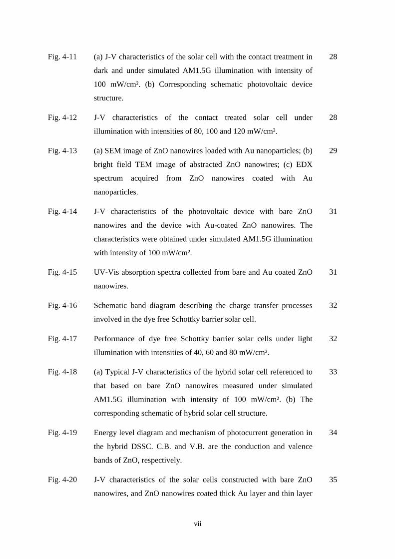
Table 4-1 Performance of the contact treated solar cell under different illumination
intensities.
Illumination intensities
(mW/cm²)
VOC (V) JSC
(mA/cm²)
FF η (%)
80 0.50 2.00 0.34 0.34
100 0.51 3.79 0.36 0.69
120 0.48 5.04 0.35 0.85
The performances of the DSSC with contact treatment under various light intensities were
investigated by adjusting the relative distance between the device and the illumination source.
Fig. 4-12 shows the J-V characteristics of the DSSC under different illumination intensities.
The parameters designated for the performance of the solar cell are listed in Table 4-1. The
short circuit current JSC exhibits an approximately linear relationship with illumination
intensity. On the other hand, the Voc and FF appear to be constant within the measured
intensity range of 80 - 120 mW/cm². The energy conversion efficiency of the DSSC increases
from 0.34 to 0.85% as the intensity increased from 80 to 120 mW/cm².
4.2.2 Dye Free Schottky Barrier Solar Cells
This section describes and evaluates the performance of Schottky barrier solar cells that are
based on ZnO nanowires coated with gold nanoparticles and an electrolyte.
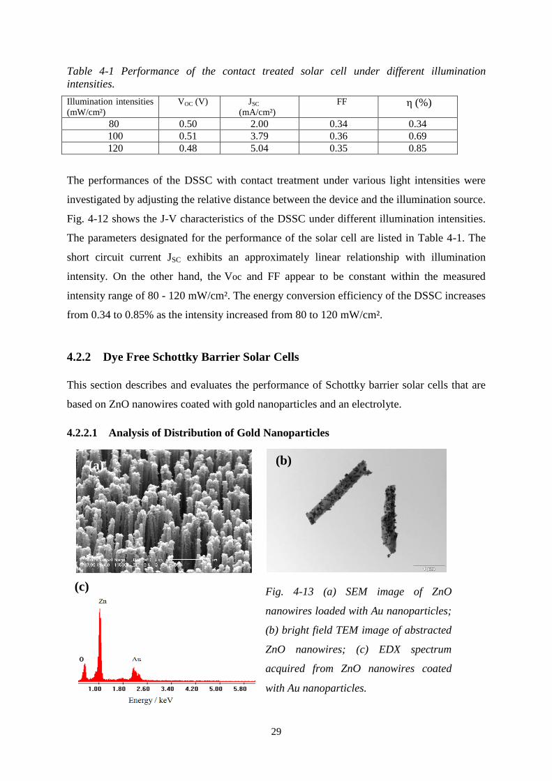
4.2.2.1 Analysis of Distribution of Gold Nanoparticles
Fig. 4-13 (a) SEM image of ZnO
nanowires loaded with Au nanoparticles;
(b) bright field TEM image of abstracted
ZnO nanowires; (c) EDX spectrum
acquired from ZnO nanowires coated
with Au nanoparticles.
(b)
(c)
(a)

30
The ZnO nanowire arrays were immersed in a mixed solution of Na3C6H5O7.2H2O (2ml, 1%)
and HAuCl4 (10ml, 0.03M). The gold ions (Au3
) reduced to neutral atoms by the citrate,
and the Au nanoparticles started to precipitate as the solution becoming supersaturated with
gold atoms. The precipitated Au nanoparticles were attached and distributed over the surfaces
of the immersed ZnO nanowires. The SEM image, in Fig. 4-13(a), shows precipitated and
anchored Au nanoparticles on the surfaces of ZnO nanowires. Obviously the surfaces of the
nanowires have become rough. However, the distribution of the Au nanoparticles over
individual nanowires is fairly uniform and the amount of Au nanoparticles occupying the
surface is conformed to the size of nanowire surface. The bright field TEM image in Fig.
4-13(b) illustrates this fact. The diameters of the precipitated Au nanoparticles on ZnO
nanowire surfaces are about 20-30 nm. The EDX compositional analysis of the nanowires in
different spots indicates chemical nature of the precipitated nanoparticles. A representative
EDX spectrum accumulated in TEM instrument in Fig. 4-13(c), comprises three peaks which
correspond to Au, Zn and O. The highly localized EDX analysis thus proves that
nanoparticles are gold, while the zinc-to-oxygen peak intensities with consideration of
corresponding atomic correction numbers give value of about one
1
/
/
0 O
znZn
O
Zn
ZI
ZI
n
n
which indicates nearly stoichiometric zinc monoxide (ZnO).
4.2.2.2 Analysis of Current Density–Voltage (J-V) Characteristics of Dye Free
Schottky Barrier Solar Cells
Current density-Voltage characteristics were measured for both Schottky barrier solar cells
based on bare ZnO nanowires and ZnO nanowires coated by gold. The device characteristics
were measured using a calibrated solar simulator under a light intensity of 100 mW/cm² (see
Fig. 4-14). The representative current density-voltage characteristic J-V measured on the light
illuminated device with Au nanoparticles shows typical values of short circuit current JSC and
open circuit voltage VOC to be 1.72 mA/cm² and 0.37 V, respectively. The fill factor FF and
energy conversion efficiency η were calculated to be 0.47 and 0.3 %, respectively. On the
other hand the J-V characteristic acquired from the device with pure ZnO nanowires almost
goes through the origin, demonstrating that practically no photocurrent is generated. This
dramatic difference is certainly associated with absence of Schottky Au/ZnO interface.

31
The mechanism of this phenomenon was investigated and explained. As confirmed in Fig.
4-15, the effect of the surface plasma resonance of Au nanoparticles can improve the optical
absorption of the ZnO nanowires in the visible light region [80]. Upon illumination, the
induced excitons in the plasma excited Au nanoparticles are dissociated and the free electrons
with equivalent energy level as that of the conduction state of the ZnO are injected into the
conduction band of the ZnO. Meanwhile, the Schottky barrier formed between the ZnO and
Au can inhibit back electron transfer from ZnO into the Au and the electrolyte. The forward
transferred electrons are transported through the ZnO nanowires and collected at the bottom
of ITO electrode. Then they are exported to an external load to complete the loop of electric
circuit. At the same time, the Au ions capture the electrons donated by the redox species
(
3/ II ) of the electrolyte to compensate their lost electrons. The triiodide (
3I ) then obtain
electrons at the counter electrode and regenerate oxidized iodide (I ). The electrons transfer
process of the redox couple should be fast and their redox potential should be sufficiently
Fig. 4-14 J-V characteristics of the
photovoltaic device with bare ZnO
nanowires and the device with Au-coated
ZnO nanowires. The characteristics
were obtained under simulated AM1.5G
illumination with intensity of 100
mW/cm².
Fig. 4-15 UV-Vis absorption
spectra collected from bare and
Au coated ZnO nanowires.
32
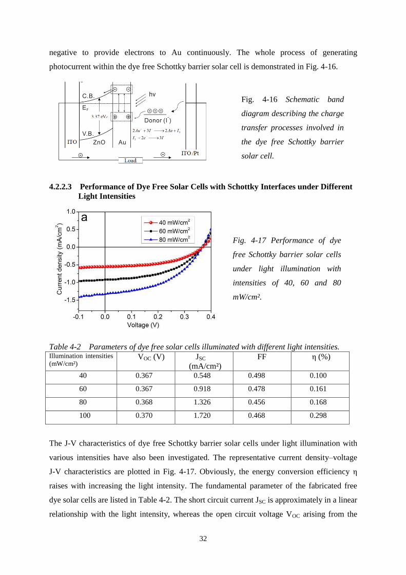
negative to provide electrons to Au continuously. The whole process of generating
photocurrent within the dye free Schottky barrier solar cell is demonstrated in Fig. 4-16.
4.2.2.3 Performance of Dye Free Solar Cells with Schottky Interfaces under Different
Light Intensities
Table 4-2 Parameters of dye free solar cells illuminated with different light intensities. Illumination intensities
(mW/cm²) VOC (V) JSC
(mA/cm²)
FF η (%)
40 0.367 0.548 0.498 0.100
60 0.367 0.918 0.478 0.161
80 0.368 1.326 0.456 0.168
100 0.370 1.720 0.468 0.298
The J-V characteristics of dye free Schottky barrier solar cells under light illumination with
various intensities have also been investigated. The representative current density–voltage
J-V characteristics are plotted in Fig. 4-17. Obviously, the energy conversion efficiency η
raises with increasing the light intensity. The fundamental parameter of the fabricated free
dye solar cells are listed in Table 4-2. The short circuit current JSC is approximately in a linear
relationship with the light intensity, whereas the open circuit voltage VOC arising from the
Fig. 4-16 Schematic band
diagram describing the charge
transfer processes involved in
the dye free Schottky barrier
solar cell.
Fig. 4-17 Performance of dye
free Schottky barrier solar cells
under light illumination with
intensities of 40, 60 and 80
mW/cm².

33
differences of the energy levels between ZnO/Au/electrolyte interfaces is maintained almost
constant. Similarly the fill factor FF is also nearly constant, since it is within the error of the
measurement accuracy of couple precent. If the value of the fill factor systematically reduces
with the increase in light intensity with small increments, then this behaviour is probably
caused by the enhanced recombination process of the electrons in the conduction band of
ZnO and triiodide in the electrolyte.
4.2.3 Characterization of Hybrid Dye Sensitized Solar Cells
This section is focused on measurement and analysis of fabricated hybrid dye sensitized solar
cells. These solar cells are based on ZnO nanowire arrays coated with Au nanoparticles and
subsequently by dye interfacing an electrolyte. The fabrication process is described above.
4.2.3.1 Performance of Designed Hybrid Dye Sensitized Solar Cells
In contrast to the discussed Schottky barrier solar cells, N719 dye was used in construction of
hybrid DSSCs. Gold nanoparticles were precipitated on the bare ZnO nanowires employing a
sol-gel method before applying the dye. The solar cell devices with the structure
schematically illustrated in Fig. 4-18(b) were analyzed to determine the device parameters,
current-voltage characteristic, and overall performance. A representative current
density–voltage (J-V) characteristic is shown in Fig. 4-18(a).
Fig. 4-18 (a) Typical J-V characteristics of the hybrid solar cell referenced to that based on
bare ZnO nanowires measured under simulated AM1.5G illumination with intensity of 100
mW/cm². (b) The corresponding schematic of hybrid solar cell structure.
(a)
(b)

34
The analysis of the J-V characteristics unambiguously indicates that the modification of the
ZnO surfaces does not improve the induced photocurrent. Compared with the J-V
characteristic of the conventionally designed DSSC, apparently, the fill factorr FF, which can
be roughly estimated form the area of the rectangle, becomes smaller for the devices
modified by Au nanoparticles. This is probably caused by the increased dissipation of power
across internal resistances. The short circuit current JSC of gold modified device is 3.08
mA/cm² which is the lower value than that of 3.8 mA/cm² measured for the DSSC based on
bare ZnO. The reduction of short circuit current density JSC may be associated with the
increased defect densities on the surfaces of ZnO nanowires produced during the Au
nanoparticles synthesis process. Although the open circuit voltage VOC is to 0.64 V, the
calculated fill factor FF and power conversion efficiency η are 0.29 and 0.58 %, respectively.
Drop of these parameters for gold modified structures is certainly caused by the lower current
densities which are evident from the J-V characteristics.
The mechanism of the photocurrent induced in the hybrid DSSCs is explained as follows.
Upon photon absorption, two simultaneous processes are involved in the process of
transferring the generated electrons from the excited dye into the conduction band of ZnO.
Firstly, the LUMO level of the dye is sufficiently negative implying that electrons can be
directly injected into the ZnO across the thin layer of Au nanoparticles by tunneling effect.
Secondly, the electrons transfer into the Au nanoparticles first, and they begin to accumulate
within Au nanoparticles. When the Fermi level of Au is raised in-line with the Fermi level of
ZnO, a quick shuttling of electrons from Au to ZnO takes place. The Schottky barrier formed
at the Au/ZnO junction can inhibit the back electron transfer event. The ZnO nanowires
provide direct paths for electrons to transport to the bottom of the ITO substrate and generate
an anodic photocurrent. Meanwhile, the generated holes in the oxidized dye are transported to
the counter electrode in the electrolyte. The whole processes are schematically illustrated by a
diagram in Fig. 4-19.
Fig. 4-19. Energy level diagram
and mechanism of photocurrent
generation in the hybrid DSSC.
C.B. and V.B. are the conduction
and valence bands of ZnO,
respectively.

35
The poor performance of the hybrid DSSCs is ascribed to the increased defects on the surface
of ZnO nanowires. The surface defects probably arising from the in-situ synthesis of Au
nanoparticles, which might act as electron recombination sites. This recombination process
then reduces the energy conversion efficiency. Annealing treatment the structure did not lead
to significant improvement in the device performance. Another possibility is the fact that Au
nanoparticles can affect the adsorption and arrangement of dye molecules over the surface of
ZnO nanowires. Aggregation and unfavourable binding of dye molecules on the ZnO surface
can result in an undesirable energy level of LOMO, which in return can induce low current
density as a consequence of the poor electron injection efficiency [77].
4.2.3.2 The Effect of the Characteristics of Gold Coatings on the Hybrid Solar Cell
Performance
The performance of the solar cell also depends on the characteristics of the thin layer of Au
nanoparticles. It was found that dense and thick layer can reduce the current density and the
fill factor FF as shown in Fig. 4-20. The reasons can originate in several effects. (i)
Aggregations of Au nanoparticles can partially block the incident light. (ii) Dense Au
nanoparticles cause high defect density on the ZnO surfaces and affect the crystallinity of
ZnO. (iii) Large density of Au nanoparticles can result in poor bindings between dye
molecules and ZnO surface. (iv) Thick Au coatings can reduce the tunnelling effect when
electrons transfer from excited dye to ZnO nanowires. Thus important implication from this
analysis is the requirement for well controlled processes associated with evolution and
characteristics of Au nanoparticles on ZnO surfaces to obtain optimal performance of hybrid
solar cells.
Fig. 4-20 J-V characteristics of the
solar cells constructed with bare ZnO
nanowires, and ZnO nanowires coated
thick Au layer and thin layer of Au
nanoparticles under simulated AM1.5G
illumination with intensity of 100
mW/cm²

36
5 Conclusions
This work presents design, fabrication, characterization and study of the produced solar cells
based on ZnO nanowires with different structural architectures. The synthesized ZnO
nanowires were aligned with the surface normal of the electrical conducting substrates. Each
nanowire is single crystalline. Although the ZnO nanowires fabricated by a thermal
evaporation method were observed to have better vertical alignment and less oxygen
vacancies, the low temperature synthesis environment and the transparent property of ITO
substrate used in the solution method are more favorable for growing ZnO nanowire arrays
used in fabrication of photovoltaic devices.
The performance of constructed conventional DSSCs has been improved after contact
interface treatment. The counter electrode was coated with platinum thin film by
electrochemical deposition to assist regeneration process of the oxidized iodide in the
electrolyte. The metal of silver with comparable work function to that of ITO was selected to
deposit on the bottom electrode to relieve contact barrier between the ITO substrate and the
electric wire leads. This way, the energy conversion efficiency η of the DSSCs improved and
was about 0.69%. It was also shown that the power conversion efficiency of the fabricated
DSSCs raised with increasing the illumination intensity.
It was found that the devices exploiting ZnO nanowires coated with Au nanoparticles can
generate photocurrent even without dye. The presence of Au nanoparticles enhanced optical
absorption in the visible range of light due to the surface plasmon resonance. The fill factor
of the designed dye free Schottky barrier solar cells achieved 0.5. After adsorption of
ruthenium dye (N719), the hybrid DSSC structures with Au nanoparticles and ZnO
nanowires showed different parameters. The open circuit voltage VOC was increased from 0.5
to 0.63 V when compared with bare ZnO nanowire based DSSCs. The reduction of short
circuit current density JSC was however reduced owning to the higher density of surface
defects on the ZnO nanowires. These defects acted as electrons recombination sites.
Therefore the overall device performance was not marginally improved. The thickness of the
Au nanoparticles coating also influenced the performance of the designed hybrid DSSCs,
which implied that further engineering and study of devices structure would be required.
37
6 References
[1] B. Regan and M. Gratzel, Nature 353(1991) 737.
[2] M. Gratzel, Nature 414 (2001) 338.
[3] M. Durr, A. Bamedi, A. Yasuda and G. Nelles, Appl. Phys. Lett. 84 (2003) 3397.
[4] M. Gratzel, Inorg. Chem. 44 (2005) 6841.
[5] H. Kohjiro, S. Hideki, T. Yasuhiro, I. Ashraful, Y. Masatoshi, S. Kazuhiro, and A. Hironori,
Langmuir, 17 (2001) 5992.
[6] T. Yoshida, K. Terada, D. Schlettwein, T. Oekermann, T. Sugiura, H. Minoura, Adv. Mater. 12
(2000) 1214.
[7] J. B. Baxter, E.S. Aydil, Appl. Phys. Lett. 86 (2005) 53114.
[8] E. Hosono, S. Fujihara, I. Honma, H. Zhou, Adv. Mater. 17 (2005) 2091.
[9] N. Taniguchi, Proc. Intl. Conf. Prod. London, Part II, British Society of Precision Engineering.
[10] C. C. Tang, S. S. Fan, P. Li, Y. M. Liu, H. Y. Dang, Mater. Lett. 51 (2001) 315.
[11] W. Lu and C. M. Lieber, J. Phys. D: Appl. Phys. 39 (2006) R387.
[12] Z. L. Wang, Appl. Phys. A 88 (2007) 7.
[13] C. M. Lieber, 2003 Mrs Bull. 28 (2003) 486.
[14] C. Zhou, J. Kong and H. Dai, Appl. Phys. Lett. 76 (2000) 1597.
[15] H, Namattsu, S. Horiguchi, M. Nagase, K. Kurihara, J. Vac. Sci. Technol. B 15(1997) 1688.
[16] C. M. Lieber and Z. Wang, Mrs Bulletin . 32 (2007) 99.
[17] M. Law, L. E. Greene, J. C. Johnson, R. Saykally and P.Yang, Nature Mater. 4 (2005) 455.
[18] H. T. Wang, B. S. Kang, F. Ren, L. C. Tien, P. W. Sadik, D. P. Norton, S. J. Pearton and J. Lin,
Appl. Phys. Lett. 86 (2005) 243503.
[19] M. Law, H .Kind, B. Messer, F. Kim and P.Yang, Angew. Chem. Int. Edn. Engl. 41 (2002) 2405.
[20] F. Patolsky, G. Zheng, O. Hayden, M. Lakadamyali, X. Zhuang and C. M. Lieber, Proceedings of
the National Academy of Science USA, 101 (2004) 14017.
[21] Y. Cui, Q. Q. Wei, H. K. Park and C. M. Lieber, Science 293 (2001) 1289.
[22] X. Duan, Y. Huang, Y. Cui, J. Wang and C. M. Lieber, Nature 409 (2001) 66.
[23] M. H. Huang, S. Mao, H. Feick, H. Q. Yan, Y. Y. Wu, H. Kind, E. Weber, R. Russo and P. Yang,
Science 292 (2001)1897.
[24] J. C. Johnson, H. J. Choi, K. P. Knutsen, R. D. Schaller, P.Yang and R. J. Saykally, Nature Mater.
1 (2002) 106.
[25] X. Duan, Y. Huang, R. Agarwal and C. M. Liber, Nature, 421 (2003) 241.
[26] S. Gradecak, F. Qian, Y. Li, H. G. Park and C. M. Lieber, Appl. Phys. Lett. 87 (2005) 173111.
[27] C. J. Barrelet, A. B. Greytak and C. M. Lieber, Nano Lett. 4 (2004) 1981.
[28] M. Law, D. J. Sirbuly, J. C. Johnson, J. Goldberger, R. J. Saykally and P.Yang, Science 305
(2004) 1269.

38
[29] R. S. Wanger and W. C. Ellis, Appl. Phys. Lett. 4 (1996) 89.
[30] H. Yu, Buhro, W.E. Adv. Mater. 15 (2003) 416.
[31] P. D. Markowitz, M. Zach, P. C. Gibbons, R. M. Penner, Buhro, W.E. J. Am. Chem. Soc. 123
(2001) 4502.
[32] M.S. Gudiksen, C. M. Liber, J. Am. Chem. Soc. 122 (2000) 8802.
[33] M. S. Gudiksen, J. Wang, C.M. Lieber, J. Phys. Chem. B 105 (2001) 4062.
[34] Y. Cui, L. J. Lauhon, M. S. Gudiksen, J. Wang, C. M. Lieber, Appl. Phys. Lett. 78 (2001) 2241.
[35] Y. Wu, P. Yang, J. Am, Chem. Soc. 123 (2001) 3165.
[36] Y. Hsu and S. Lu, J. Phys. Chem. B 109 (2005) 4398.
[37] Y. F. Zhang, Y. H. Tang, N. Wang, D. P. Yu, C. S. Lee, I. Bello, S. T. Lee, Appl. Phys. Lett. 72
(1998) 1835.
[38] N.W. Ng, Y. H. Tang, C. S. Lee, S. T. Lee, Phys. Rev. B 58 (1998) R16024.
[39] S. T. Lee, Y. F. Zhang, N. Wang, Y. H. Tang, I. Bello, C.S. Lee, Y. W. Chung, J. Mater.Res.14
(1999) 4503.
[40] S. T. Lee, N. Wang, C. S. Lee, Mater. Sci. Eng. A 16 (2000) 286.
[41] S.T. Lee, N. Wang, Y.F. Zhang, Y.H. Tang, MRS Bull. 24 (1999) 36.
[42] R.Q. Zhang, Y. Lifshitz, S.T. Lee, Adv. Mater. 15 (2003) 635.
[43] R.Q. Zhang, T.S. Chu, H.F. Cheung, N. Wang, S.T. Lee, Phys Rev. B 64 (2001) 113304.
[44] Y. F. Zhang, Y.H. Tang, H.Y. Peng, N. Wang, C.S. Lee, I. Bello, S.T. Lee, Appl.Phys.Lett. 75
(1999) 1842.
[45] Z. W. Pan, H.L. Lai, C. K. Frederick, Au, X. F. Duan, S.S. Xie, Adv.Mater.12 (2000) 1186.
[46] R. S. Wagner, W. C. Ellis, Appl. Phys Lett. 4 (1964) 1964.
[47] D. P. Yu, Q. L. Hang, Y. Ding, H.Z. Zhang, Z.G. Bai, Appl. Phys. Lett. 73 (1998) 3458.
[48] H. Namattsu, S. Horiguchi, M. Nagase, K. Kurihara, J. Vac. Sci. Technol. B 15 (1997) 1688.
[49] L. J. Lauhon, M. S. Gudiksen and C. M. Lieber, Phil. Trans. R. Soc. Lond. A 362 (2004) 1247.
[50] W. Lu, and C. M. Lieber, J. Phys. D: Appl. Phys. 39 (2006) R387.
[51] K. A. Dick, K. Deppert, M. W. Larsson, T. Martensson, W. Seifert, L. R. Wallenberg and L.
Samuelson, Nature Mater. 3 (2004) 380.
[52] D. C. Look, Mater. Sci. Eng. B 80 (2001) 383.
[53] H. Cao, et al., Phys. Rev. Lett. 84 (2000) 5584.
[54] M. H. Huang, et al., Science 292 (2001) 1897.
[55] Z. L. Wang, J.H. Song, Science 312 (2006) 242.
[56] Z. L. Wang, Appl. Phys. A 88 (2007) 7.
[57] M. H. Zhao, Z. L. Wang, S. X. Mao, Nano Lett. 4 (2004) 587
[58] J. A. Venables, Introduction to Surface and Thin Film Processes, Cambridge University Press,
Chembridge 2000, p.4.
[59] W. I. Park, D. H.Kim, S. W. Jung, and G.C. Yi, App. Phys. Lett. 80 (2002) 4232.
39
[60] B. Fuhrmann, H. S. Leipner, H. R. Hoche, L. Schubert, P. Werner, U. Gosele, Nano Lett. 5 (2005)
2524.
[61] S. K. Chan, Y. Cai, I. K. Sou, and N. Wang, J. Cryst. Growth, 278 (2005) 146.
[62] M. T. Bjork, B. J. Ohlsson, T. Sass, A. I. Persson, C. Thelander, M. H. Magnjusson, K. Depper,
L. R. Wallenberg, and L. Samuelson, Appl. Phys. Lett. 80 (2002) 1058.
[63] G. F. Zheng, W. Lu, S. Jin, C. M. lieber, Adv. Mater. 16 (2004) 1890.
[64] S. D. Hersee, X. Sun, and X. Wang, Nano Lett. 6 (2006) 1808.
[65] M. Law, L. E. Greene, A. Radenovic, T. Kuykendall, J. Liphardt, and P. Yang, J. Phys. Chem. B
110 (2006) 22653.
[66] W. Mai, P. Gao, C. Lao, Z. Wang, , A. K. Sood, D. L. Polla, M. B. Soprano, , Chem. Phy. Lett.
460 (2008) 253.
[67] Report of the basic energy science workshop on solar energy utilization, (2005) 18.
[68] M. K. Nazeeruddin, P. Péchy, T. Renouard, S. M. Zakeeruddin, R. Humphry-Baker, P. Comte, P.
Liska, L. Cevey, E. Costa, V. Shklover, L. Spiccia, G. B. Deacon, C.A. Bignozzi, and M. Grätzel,
J. Am. Chem. Soc. 123 (2001) 1613.
[69] P. Wang, et al. Nature Mater. 2 (2003) 402.
[70] A. J. Frank, N. Kopidakis, V Lagemaat, Chem. Rev. 248 (2004) 1165.
[71] T. Renouard, R. A. Fallahpour, Md. K. Nazeeruddin, R. Humphry-Baker, S. I. Gorelsky, A. B. P.
Lever, and M. Grätzel, Inorg. Chem. 41 (2002) 367.
[72] K. Hara, M. Kurashige, Y. Dan-Oh, et al. New J. Chem. 27 (2003) 783.
[73] L. E. Greene, M. Law, D. H. Tan, M. Montano, J. Goldberger, G. Somorjai, and P. Yang, Nano
let. 5 (2005) 1231.
[74] C. Geng, Y. Jiang, Y. Yao, X. Meng, J. A. Zapien, C. S. Lee, Y. Lifshitz, and S. T. Lee, Adv.
Fun. Mat. 14 (2004) 589.
[75] B. J. Jin, S. H. Bae, S. Y. Lee, and S. Im, Mater. Sci. Eng. B 71 (2007) 301.
[76] B. Lin, Z. Fu, and Y. Jia, Appl. Phys. Lett. 79 (2001) 943.
[77] V. Thavasi, V. Renugopalakrishnan, R. Jose, S. Ramakrishna, Mater. Sci. Eng. R 63 (2009) 81.
[78] S. E. Shaheen, C. J. Brabec, N. S. Sariciftci, F. Padinger, T. Fromherz, J. C. Hummelen, Appl.
Phys. Lett. 78 (2001) 841.
[79] C. J. Brabec, A. Cravino, D. Meissner, N. S. Sariciftci, T. Fromherz, M. T. Rispens, L. Sanchez,
J. C. Hummelen, Adv. Funct. Mater. 11 (2001) 374.
[80] X. Hu, D. J. Blackwood, J. Electroceram. 16 (2006) 593.