competitive and cost effective copper/low-k interconnect ... · competitive and cost effective...
TRANSCRIPT
Competitive and Cost Effective Copper/Low-kInterconnect (BEOL) for 28nm CMOS Technologies1R. Augur, 1C. Child, 2J.H. Ahn, 1aT.J. Tang, 3L. Clevenger, 1D. Kioussis, 6H. Masuda, 1aR. Srivastava, 4Y. Oda, 6H. Oguma,3R. Quon, 5B. Kim, 1aH. Sheng, 6S. Hirooka, 1R. Gupta, 3A. Thomas, 1aS.M. Singh, 1aQ. Fang, 7R. Schiwon, 5B. Hamieh, 3E. Wornyo, 3S. Allen, 7E. Kaltalioglu, 5G. Ribes, 1aG. Zhang, 1T. Fryxell, 6A. Ogino, 6E. Shimada, 4H. Aizawa, 4H. Minda, 7S.O. Kim, 6T. Oki, 6K. Fujii, 7M. Pallachalil, 4T. Takewaki. 3C.K. Hu, 3B. Sundlof, 1D. Permana, 1T. Bolom, 3B. Engel, 1C. Labelle, 3B. Sapp, 3T. Nogami, 3A. Simon, 3H. Shobha, 3S. Gates, 3E.T. Ryan, 3G. Bonilla, 3T. Daubenspeck, 3T. Shaw, 3G. Osborne, 3A. Grill, 3D. Edelstein, 3D. Restaino, 3S. Molis, 3T. Spooner, 5P. Ferreira, 3G. Biery, 5R. Sampson
1 GLOBALFOUNDRIES, 1a GLOBALFOUNDRIES Singapore, 2Samsung Electronics, 3IBM Microelectronics, 4Renesas Electronics, 5STMicroelectronics, 6Toshiba America, 7Infineon Technologies.
October 5, 2010
email: [email protected]
Contents
§Technology Definition.§Challenges of node-on-node scaling for BEOL
interconnect.§Process Optimization (ULK and Etch Profile).§Electrical Performance.§Yield Factors.§Reliability (EM and TDDB).§Summary.
2October 5, 2010 GLOBALFOUNDRIES, 28nm BEOL Integration
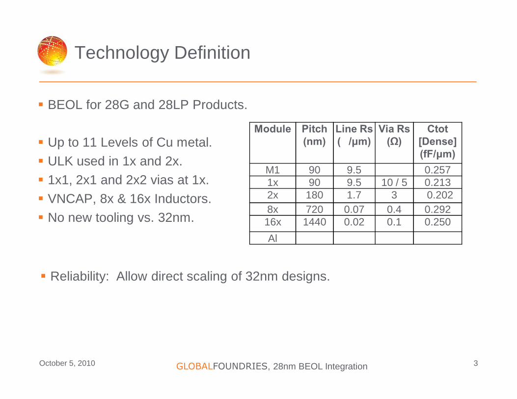
Technology Definition
§ BEOL for 28G and 28LP Products.
§ Up to 11 Levels of Cu metal.§ ULK used in 1x and 2x.§ 1x1, 2x1 and 2x2 vias at 1x.§ VNCAP, 8x & 16x Inductors.§ No new tooling vs. 32nm.
3October 5, 2010
Module Pitch (nm)
Line Rs(Ω/μm)
Via Rs(Ω)
Ctot [Dense] (fF/μm)
M1 90 9.5 0.2571x 90 9.5 10 / 5 0.2132x 180 1.7 3 0.2028x 720 0.07 0.4 0.29216x 1440 0.02 0.1 0.250Al
§ Reliability: Allow direct scaling of 32nm designs.
GLOBALFOUNDRIES, 28nm BEOL Integration
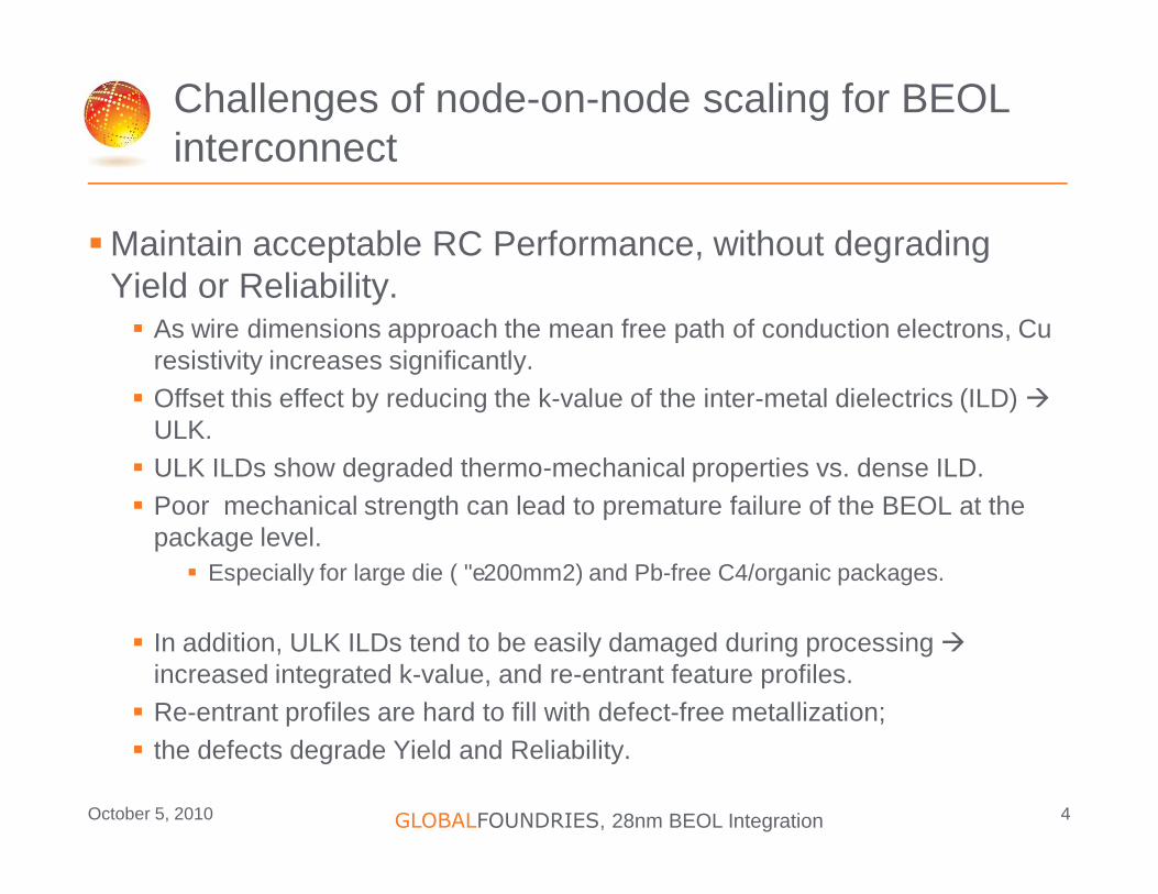
Challenges of node-on-node scaling for BEOL interconnect
§Maintain acceptable RC Performance, without degrading Yield or Reliability. § As wire dimensions approach the mean free path of conduction electrons, Cu
resistivity increases significantly.§ Offset this effect by reducing the k-value of the inter-metal dielectrics (ILD) à
ULK.§ ULK ILDs show degraded thermo-mechanical properties vs. dense ILD.§ Poor mechanical strength can lead to premature failure of the BEOL at the
package level. § Especially for large die ( ≥ 200mm2) and Pb-free C4/organic packages.
§ In addition, ULK ILDs tend to be easily damaged during processing àincreased integrated k-value, and re-entrant feature profiles.§ Re-entrant profiles are hard to fill with defect-free metallization;§ the defects degrade Yield and Reliability.
4October 5, 2010 GLOBALFOUNDRIES, 28nm BEOL Integration
Process Optimization
§Trench First Hard Mark (TFHM) Integration Approach selected for minimum pitch ULK module.§Properties of ULK optimized for mechanical strength,
adhesion, k-value and damage resistance.§Feature profile optimized to enable PVD-only liner/seed
deposition for defect-free metal fill.§Cu-alloy seed used to meet EM targets.§TFHM approach used to provide tighter control of via-top to
adjacent metal spacing, in order to address TDDB.
5October 5, 2010 GLOBALFOUNDRIES, 28nm BEOL Integration
Process Optimization (ULK)
6October 5, 2010
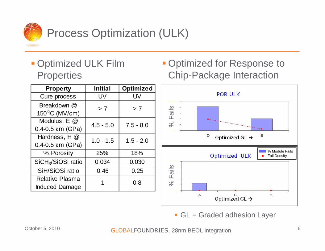
§Optimized ULK Film Properties
§Optimized for Response to Chip-Package Interaction
§ GL = Graded adhesion Layer
Property Initial OptimizedCure process UV UVBreakdown @
1500C (MV/cm)> 7 > 7
Modulus, E @ 0.4-0.5 μm (GPa) 4.5 - 5.0 7.5 - 8.0
Hardness, H @ 0.4-0.5 μm (GPa)
1.0 - 1.5 1.5 - 2.0
% Porosity 25% 18%SiCH3/SiOSi ratio 0.034 0.030SiH/SiOSi ratio 0.46 0.25Relative Plasma Induced Damage
1 0.8
o
GLOBALFOUNDRIES, 28nm BEOL Integration
% Module FailsFail Density
% F
ails
% F
ails
7October 5, 2010
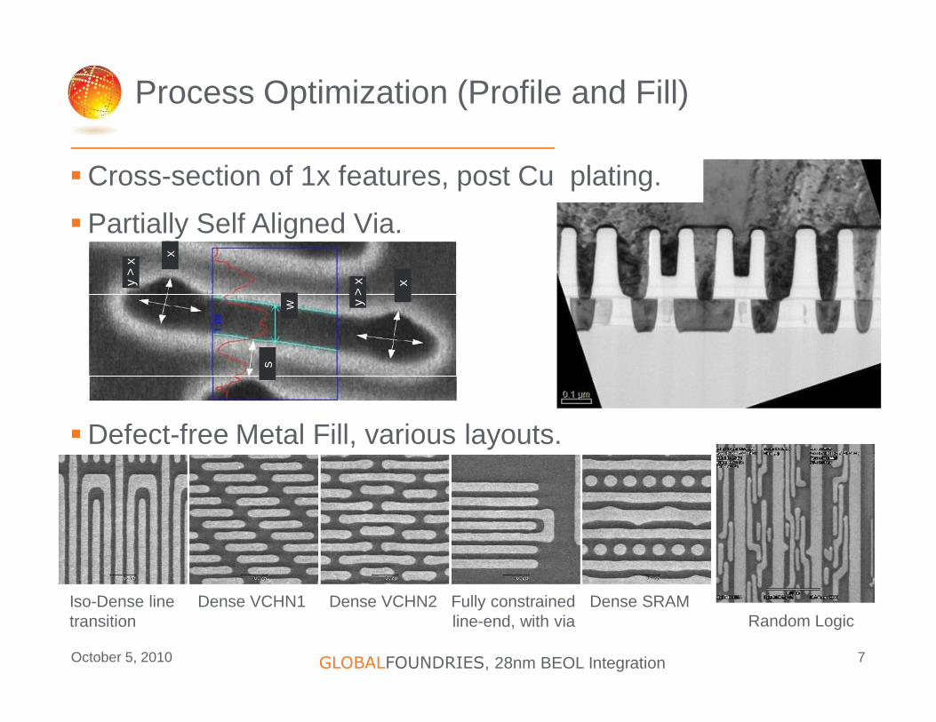
§Cross-section of 1x features, post Cu plating.
§Partially Self Aligned Via.
§Defect-free Metal Fill, various layouts.
Iso-Dense line Dense VCHN1 Dense VCHN2 Fully constrained Dense SRAMtransition line-end, with via
Process Optimization (Profile and Fill)
Random Logic
GLOBALFOUNDRIES, 28nm BEOL Integration
y >
x x
s
w y >
x x
Electrical Performance
8October 5, 2010
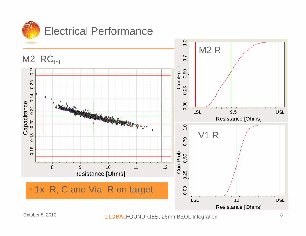
§ 1x R, C and Via_R on target.
GLOBALFOUNDRIES, 28nm BEOL Integration
8 9 10 11 12Resistance [Ohms]
Cap
acita
nce
0.16
0
.18
0.
20
0.2
2 0
.24
0.
26
0.2
8
M2 RCtot
M2 R
7E LSL 9.5 USLResistance [Ohms]
Cum
Pro
b0.
00
0.2
5
0.5
0
0.7
1.0
7E LSL 10 USLResistance [Ohms]
Cum
Pro
b0.
00
0.2
5
0.5
0
0.7
0
1.0
V1 R
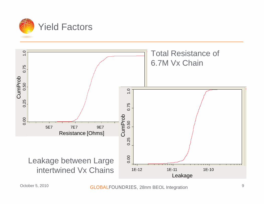
Yield Factors
9October 5, 2010 GLOBALFOUNDRIES, 28nm BEOL Integration
Total Resistance of 6.7M Vx Chain
Leakage between Large intertwined Vx Chains
5E7 7E7 9E7 1.1E8Resistance [Ohms]
Cum
Pro
b0.
00
0.25
0.5
0
0
.75
1.0
Cum
Pro
b0.
00
0.25
0.5
0
0
.75
1.0
1E-12 1E-11 1E-10Leakage

Reliability – Electro-Migration
10October 5, 2010
§Via and Line Depletion EM pass with margin.
GLOBALFOUNDRIES, 28nm BEOL Integration
0.5 1 5 10 50 100 500 1000Time to Fail (hrs.)
1
10
50
90
99
99.9
elitnecreP
10% dR/R,normalized to 25mA/um2 & 300C V1->M2 (narrow) , I=0.105mA, T=300 C 28nm Highlander Lot 25HI16
AAAAAAAAAAAAAAAAAAAAAAA
BBBBBBBBBBBBBBBBBBBBB 0VSEB4
A 0XSEC5Comment300C
10% dR/R
V1-M2 (45nm)
Lifetime
Per
cent
Fai
ls
0.5 1 5 10 50 100 500 1000Time to Fail (hrs.)
1
10
50
90
99
99.9
elitnecreP
10% dR/R,normalized to 25mA/um2 & 300C V2->M2 (narrow) , I=0.105mA, T=300 C 28nm Highlander Lot 25HI16
AAAAAAAAAAAAAAAAAAA
BBBBBBBBBBBBBBBBBBBBBB
B 0VSEB4A 0XSEC5
Comment300C10% dR/R
Lifetime
Per
cent
Fai
ls
V2-M2 (45nm)
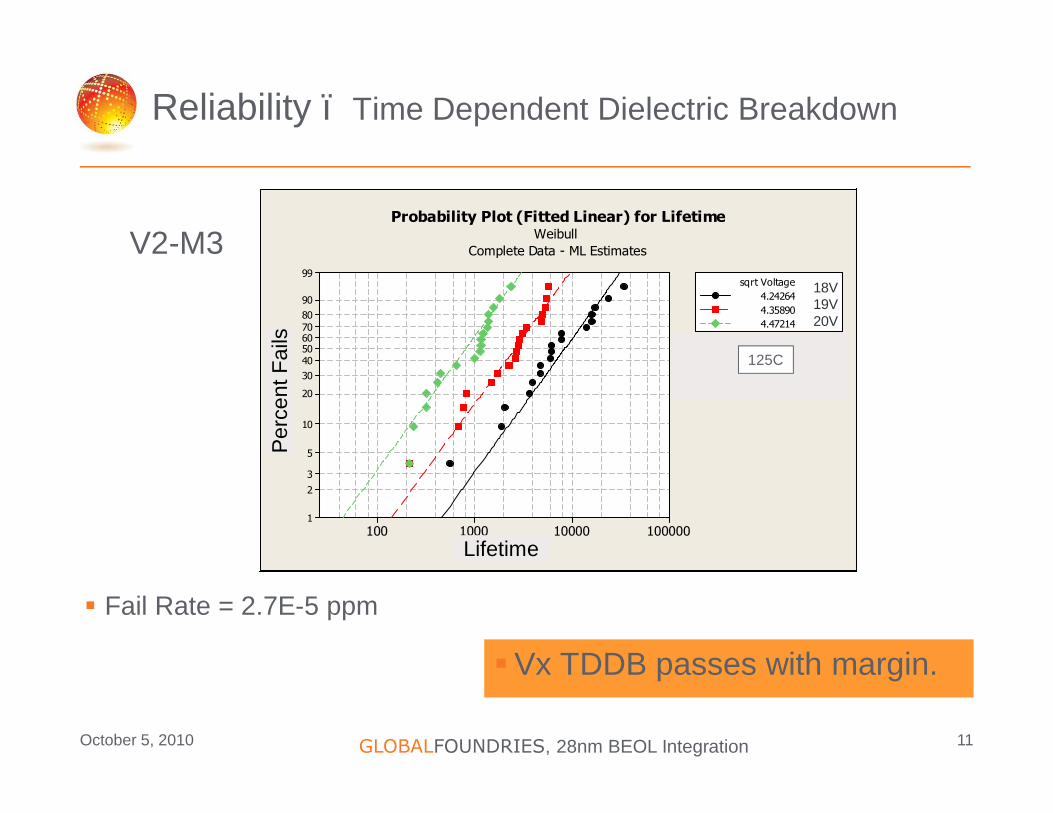
§ Fail Rate = 2.7E-5 ppm
Reliability – Time Dependent Dielectric Breakdown
11October 5, 2010
§Vx TDDB passes with margin.
GLOBALFOUNDRIES, 28nm BEOL Integration
V2-M3
100000100001000100
99
90807060504030
20
10
5
3
2
1
Lifetime
Perc
ent 1.44806 11056.5 1.359 18 0
1.44806 3366.1 0.917 18 01.44806 1057.0 1.521 18 0
Shape Scale A D* F CTable of S tatistics
4.242644.358904.47214
sqrt Voltage
Probability Plot (Fitted Linear) for Lifetime
Complete Data - ML EstimatesWeibull
18V19V20V
125C
Lifetime
Per
cent
Fai
ls

Summary
§A cost effective Interconnect technology was presented, for 28G and 28LP applications.§ 1x, 2x, 8x and 16x modules can be combined up to 11 total
copper wiring levels. §The technology uses conventional tools and processes for
metallization. §ULK inter-metal dielectric is used at minimum pitch (1x) and
2x levels. §Properties of the ULK were optimized for mechanical
strength, adhesion, k-value and damage resistance.§Full capacitance entitlement of the ULK was demonstrated.§Etch profile was optimized to enable defect-free metal fill. §High yields and robust reliability were achieved.
12October 5, 2010 GLOBALFOUNDRIES, 28nm BEOL Integration

Acknowledgements
Trademark Attribution
GLOBALFOUNDRIES, the GLOBALFOUNDRIES logo and combinations thereof are trademarks of GLOBALFOUNDRIES Inc. in the United States and/or other jurisdictions. Other names used in this presentation are for identification purposes only and may be trademarks of their respective owners.
©2009 GLOBALFOUNDRIES Inc. All rights reserved.
This work was performed at the IBM Microelectronics Div., Semiconductor Research & Development Centre, Hopewell Junction, NY 12533. The authors would like to thank W. Chu, I. Brooks, J. Benedict and their teams for technical assistance. The authors would also like to thank E. Kaste, R. Divakaruni, P. Gilbert, G. Patton and S. Venkatesan for their support.
13October 5, 2010 GLOBALFOUNDRIES, 28nm BEOL Integration