contract no. fa9550-07-c-0034 final report prepared for
TRANSCRIPT

Contract No. FA9550-07-C-0034
“High Critical Current in Metal Organic Derived YBCO Films”
Final Report
Prepared for:
Dr. Harold Weinstock Air Force Research Laboratory
Air Force Office of Scientific Research
Prepared by:
Dr. Xiaoping Li American Superconductor Corporation
64 Jackson Road Devens, MA 01434

Report Documentation Page Form ApprovedOMB No. 0704-0188
Public reporting burden for the collection of information is estimated to average 1 hour per response, including the time for reviewing instructions, searching existing data sources, gathering andmaintaining the data needed, and completing and reviewing the collection of information. Send comments regarding this burden estimate or any other aspect of this collection of information,including suggestions for reducing this burden, to Washington Headquarters Services, Directorate for Information Operations and Reports, 1215 Jefferson Davis Highway, Suite 1204, ArlingtonVA 22202-4302. Respondents should be aware that notwithstanding any other provision of law, no person shall be subject to a penalty for failing to comply with a collection of information if itdoes not display a currently valid OMB control number.
1. REPORT DATE 31 OCT 2010 2. REPORT TYPE
3. DATES COVERED 02-10-2007 to 11-01-2009
4. TITLE AND SUBTITLE High Critical Current in Metal Organic Derived YBCO Films
5a. CONTRACT NUMBER
5b. GRANT NUMBER
5c. PROGRAM ELEMENT NUMBER
6. AUTHOR(S) 5d. PROJECT NUMBER
5e. TASK NUMBER
5f. WORK UNIT NUMBER
7. PERFORMING ORGANIZATION NAME(S) AND ADDRESS(ES) American Superconductor Corporation,64 Jackson Road,Devens,MA,01434
8. PERFORMING ORGANIZATIONREPORT NUMBER
9. SPONSORING/MONITORING AGENCY NAME(S) AND ADDRESS(ES) 10. SPONSOR/MONITOR’S ACRONYM(S)
11. SPONSOR/MONITOR’S REPORT NUMBER(S)
12. DISTRIBUTION/AVAILABILITY STATEMENT Approved for public release; distribution unlimited
13. SUPPLEMENTARY NOTES
14. ABSTRACT
15. SUBJECT TERMS
16. SECURITY CLASSIFICATION OF: 17. LIMITATION OF ABSTRACT Same as
Report (SAR)
18. NUMBEROF PAGES
17
19a. NAME OFRESPONSIBLE PERSON
a. REPORT unclassified
b. ABSTRACT unclassified
c. THIS PAGE unclassified
Standard Form 298 (Rev. 8-98) Prescribed by ANSI Std Z39-18

American Superconductor Corporation Contract FA9550-07-C-0034 Final Report
2
EXECUTIVE SUMMARY:
The Phase II STTR Project focused on optimization of the Metal Organic Deposition (MOD) process for deposition thick, high critical current YBCO films for use in the Second Generation (2G) YBCO coated conductor wires. The project successfully extended the YBCO thickness to > 2 μm using a multi-coat process. A critical current of 560 A/cm-width (77K, self-field) was achieved in a 2μm thick, rare earth doped YBCO film. The thick film, multi-coat process coating, decomposition and reaction process was successfully transferred to American Superconductor’s wide-web (40 mm) manufacturing line. 2G wires with 1.4 μm thick, rare earth doped YBCO films were produced in lengths to 100 meters. In addition, a modified decomposition process was developed for Metal Organic based YBCO precursors that resulted in an increase in the maximum single-coat thickness to >1.2 μm. A critical current approaching 450 A/cm-width was achieved in short length 1.2 μm, single-coat YBCO film.

American Superconductor Corporation Contract FA9550-07-C-0034 Final Report
3
BACKGROUND
The Second Generation (2G) high temperature superconducting (HTS) YBCO wire is a versatile, potentially transformational, technology for a number of military and commercial applications. However, anticipated military applications such as energy dense electric propulsions systems (including motor and adjustable speed motor drives), directed energy weapons (including gyrotron magnet and power supply) and energy dense power supply systems (including generator and power conditioning electronic modules) and commercial applications such as motors, generators, transformers, fault current limiters, superconducting magnetic energy storage, and power transmission lines [ 1 ] require improvement in the performance of 2G wires before these applications are broadly realized. Three main regimes of operation for targeted applications for 2G wires include cables at 77 K; self-field, military products at 65 – 77 K, 2 – 3T; and commercial motors at 30 – 50 K, 1 – 3 T. Figure 1 shows the typical critical current of an AMSC 2G conductor (YBCO [0.8μm]/CeO2/YSZ/Y2O3/NiW - black lines) as a function of the applied magnetic field (Hperp) and temperature at the beginning of the STTR project. Targeted Ic performance for the three main regimes are indicted in the figure. Also shown in the figure (red dots) are the Ic values at 77 K and 65 K of a 2 μm thick YBCO-MOD film developed during Phase I program. It is seen that even with the 2 μm thick pure YBCO-MOD film that carries Ic of 510 A/cm-W @ 77 K, self-field, the weak in-field Ic performance of pure YBCO-MOD film would limit this type of wire to the cable application only. To achieve broad applications of HTS wires, enhanced in-field Ic with H//c is required. By the end of Phase I project, RE nano-dots were introduced into the AMSC’s 0.8 μm baseline process. As comparison, the Ic-B performance of 0.8 μm MOD films with and without RE-nanodots is also shown in Figure 1 in blue curves. The comparison clearly indicates the c-axis in-field Ic benefit of the RE-nanodots composition. Therefore, the RE-nanodots doping was incorporated in the Phase II thick film program to achieve further improvements in the critical current for broad-scale commercialization of 2G superconducting wire.
The obvious route to higher Ic is to increase the thickness, t, of the YBa2Cu3O7-x (YBCO) layer. However, in practice, significant reductions of Jc with increasing t are observed in YBCO films [2,3,4,5,6]. The decrease in Jc with increasing thickness can arise for a variety of reasons, including loss of texture in the growing film, increased porosity and secondary phase formation, changes in precursor composition or random nucleation of YBCO. Preventing the decrease in Jc requires the ability to control the YBCO nucleation and growth process, particularly in reel-to-reel manufacturing equipment. During Phase I, a “three-step” conversion process was developed to de-convolute the individual effect of precursor pre-conditioning, nucleation and growth to the microstructure evolution and Ic performance of thick YBCO films. A critical Ic of 492/cm-w was achieved through optimizing each of the three steps on short sample with triple-coat pure YBCO (without RE nanodots addition) films at a thickness of 2μm.
Phase II project focused on further optimization of the conversion process of thick YBCO film with nanodots addition, understanding the through thickness Jc degradation mechanism of thick MOD-YBCO films, and transferring the thick film conversion process into AMSC’s pilot manufacturing process.

American Superconductor Corporation Contract FA9550-07-C-0034 Final Report
4
Fig. 1. Critical current density (per unit width) of AMSC 2G wires and as function of applied field (H
perpendicular to wire face) and temperature (black curve: YBCO[0.8μm]/CeO2/YSZ/Y2O3/NiW; blue curve: RE-YBCO[0.8μm]/CeO2/YSZ/Y2O3/NiW). Operating temperature and magnetic fields of targeted applications are indicated. Red dots represent improvements in Ic achieved during the Phase I project with 2μm thick pure Y123-MOD film on RABiTS.
TECHNICAL APPROACH AND PROGRESS AGAINST PHASE II OBJECTIVES The overall objective of the Phase II Project was to demonstrate the practical
manufacturing of continuous lengths of 344 superconductor wire with a critical current exceeding 200 A (>500 A/cm-w) at 77K, self-field using a low-cost solution-based deposition process for the YBCO layer.
AMSC’s approach for the deposition of YBCO films is based on the ex situ conversion of a fluorine-based precursor deposited by a low-cost the MOD technique employing on a trifluoroacetate (TFA) based precursor [7, 8]. The route to higher Ic in MOD-based films is to increase the thickness (t) of the YBCO layer and maintain the Jc through film thickness. For ex-situ conversion of thick a MOD film, the challenge is three-fold: 1) coating and decomposition of defect free thick precursor film of sufficient thickness; 2) control of thick film epitaxial nucleation; 3) control of through thickness YBCO growth.
The Phase II project focused on (1) developing a robust multi-coat process and increasing the thickness of the single-coat process. (2) characterization and optimization of the nucleation and growth stages of both the single and multi-coat films and (3) transferring the thick film coating-decomposition-reaction process to a long length roll-to-roll manufacturing process.
The major accomplishments of the Phase II project include:
• A critical current of 560 A/cm-w was achieved in a 2 μm MOD film (660 A/cm-w was demonstrated in a 2 μm MOD film in a separately supported effort [9]).
• The maximum thickness of the single-coat MOD film was increased by 50% to 1.2 μm
0 1 2 3 4 5 6 7 810
100
1000
0.1
1.0
10.0 RE50, 27K RE50, 65K RE50, 77K
Y123: 27K Y123: 65K Y123: 77K
Jc (M
A/cm
2)I c (Α/c
m-W
)
μ0H (T)
Cables
Military
Commercial Motor/Generator

American Superconductor Corporation Contract FA9550-07-C-0034 Final Report
5
• The thick film multi-coat and single-coat coating/decomposition processes were successfully demonstrated in AMSC’s 2G roll-to-roll manufacturing line
• A thick film conversion process for a 1.4 μm film was successfully demonstrated in AMSC’s pilot roll-to-roll YBCO manufacturing furnace
• Multiple 100 meter lengths of 2G wire, with an Ic exceeding 300 A/cm-w, were fabricated in AMSC’s 2G pilot manufacturing line.
The maximum thickness film that could be processed during the Phase II project was limited to ~ 1.5 μm due to the length of the pilot-roll-to-roll conversion furnace. This it was not possible to reach the ultimate project goal of 500 A/cm-w in long lengths. However, the fundamental knowledge gained during the Phase II project was used in designing a new conversion furnace that will be capable of processing the thick films required for the higher Ic.
PHASE II RESULTS
Task 1. Process Development for 600A/cm-w YBCO Films In order to further increase Ic performance of thick MOD film, the Phase II effort focused
on process development of double and triple-coat MOD films with rare earth nanodot additions. Processing of the thick YBCO samples in Task 1 was carried out using a new short sample reaction furnace based on a design developed in the Phase I project. In the new furnace, the short sample is moved through the various temperature zones at a variable speed, thus simulating the temperature profiles and gas dynamics of AMSC’s reel-to-reel manufacturing furnace. The process developed in this system was readily transferable to the manufacturing equipment. Figure 2 shows the schematics of the moving, short sample reaction furnace used for processing MOD films with a thickness in the range of 0.8 μm to 2μm.
Fig 2. Schematic illustration of the moving furnace design developed for processing
short samples in the Phase II project.
A design of experiments approach was used to study the effect of key process parameters including the temperature, ramp rate, flow rate, pO2, pH2O and time in each of the 4 segments of the conversion process, illustrated in Figure 3, as a function of film thickness. S1 corresponds to the precursor annealing, S2 to YBCO nucleation, S3 to YBCO growth and S4 to the sample cool-down. Samples were quenching at various times throughout the process and analyzed by surface and cross-sectional microscopy, x-ray analysis and Ic measurements. The major conclusions from the experiments were that the performance of the film is strongly dependent on the initial temperature ramp and the overall growth rate of the YBCO.

American Superconductor Corporation Contract FA9550-07-C-0034 Final Report
6
Fig 3. Schematic illustration of the temperature-time profile developed for the thick
film processing in the moving, short sample furnace.
Figure 4 shows the effect of the ramp rate in S1 on the microstructure, texture and critical current (77K, self-field) of a 2 μm thick, triple-coat MOD film with an architecture of (from top to bottom) Y123-0.6μm/Y123-0.6μm/Y(Dy)123-0.8μm. With a fast ramp rate, excess fluoride remains when the film reaches the high temperature, leading to a low nucleation rate, excessive reaction between the precursor and CeO2 buffer surface and the formation of an undesirable YBCO texture (indicated by (103)/(013) XRD peaks in Figure. 4). In contrast, a slow ramp rate results in a low fluoride concentration, leading to the formation of random grains and strong (103)/(013) XRD peaks as seen in Figure 4 Since the total fluoride content of the film is dependent on the film thickness, the the S1 ramp rate is strongly dependent on the starting film thickness and composition. When the fluoride concentration is controlled correctly, the film is highly (00l) textured with a clean microstructure. These data are consistent with the key learning in Phase I, which showed that over processed precursor films lead to random YBCO nucleation.
Fig. 4 Optical micrographs (surface) and Ic performance for S1 ramp rates generating
low, optimized and high fluoride concentrations in the precursor (Y123-0.6μm/Y123-0.6μm/Y(Dy)123-0.8μm) film. X-ray data show effect of S1 ramp on the YBCO texture.

American Superconductor Corporation Contract FA9550-07-C-0034 Final Report
7
Figure 5 shows the Ic dependence of a 2 μm thick, triple-coat film (Y123-0.6μm/Y123-0.6μm/Y(Dy)123-0.8μm) on the pH2O during the S3. Since the pH2O has a direct influence on the film conversion rate, the data indicate that control of growth rate in S3 is critical to the YBCO quality.
Fig.5. Effect of pH2O during S3 on the critical current of triple-coat 2μm MOD film
with architecture Y123-0.6μm/Y123-0.6μm/Y(Dy)123-0.8μm (top to bottom).
Optimization of the key process variables for each of the segments was carried out for double-coat and triple-coat films in order to maximize overall Ic and the through thickness properties. Using the optimized process conditions, a critical current of 500 A/cm-w (77K, self-field) was obtained with a 1.4 μm, double-coat sample and a critical current of 560 A/cm-w (77K, self-field)was achieved in a 2 μm, triple-coat film.
Ion milling experiments were carried out to determine the through thickness Jc dependence of the multi-coat films. The experiments were carried out, at Florida State University, by progressively ion milling through the sample thickness and measuring the Ic after each milling step as illustrated in Figure 6.
Fig.6. Schematic illustration of the ion milling approach used to determine the
through thickness performance of the HTS films.
Figure 7 shows the improvement in through thickness Jc achieved through optimization of the process parameters during the Phase II program. In general, the measured Jc was constant in the first layer and then decreased in the upper layer (s) as shown in Figure 7 for a 1.4 μm, double coat film. The decrease in Jc is generally associated with location of the interface between the individual layers which is seen in the cross-section of a fully processed -cost film in Figure 8.
200
250
300
350
400
450
500
550 Y/Y/RE (2μm)
Ic (7
7K, s
f) (
A/c
m-W
)
S3: pH2O

American Superconductor Corporation Contract FA9550-07-C-0034 Final Report
8
(a) (b)
Fig. 7. Through thickness Jc measured on double-coat YBCO films using (a) initial process conditions derived from 0.8 μm thick films and (b) process parameters optimized for thick films.
(a) (b)
Fig. 8. (a) Z-contrast STEM image and (b) and elemental mapping of a fully converted double-coat MOD film with an architecture of Y123-0.6μm/Y(Dy)123-0.8μm (top to bottom).
In order to establish the fundamental cause for the lower Jc in the upper region of the films, quench studies were carried out as illustrated in Figure 9. The quenched samples were examined by Raman spectroscopy, cross-sectional SEM-TEM and x-ray analysis. The quench studies showed that a copper rich layer forms in the initial precursor film at the boundary between the individual layers as shown in Figure 10. During the subsequent reaction process, this copper rich region converts to a semi-continuous CuO layer that blocks the uniform growth of the YBCO growth front As a result, when the YBCO growth reaches the CuO layer (in S3), the uniform growth is disrupted, proceeds through openings in the CuO layer and then grows laterally over the surface of the CuO layer. As a result, when the upward YBCO growth resumes there is a loss of YBCO texture which is reflected in the reduced Jc. This process is seen in Figure 11 which shows the cross-sectional images of the YBCO growth across the interface boundary.

American Superconductor Corporation Contract FA9550-07-C-0034 Final Report
9
Fig.98. Schematic showing location of quenches used to study the growth of YBCO.
(a) (b)
Fig. 10. (a) Cross-section SEM and (b) elemental mapping of a triple-coat precursor film after decomposition showing the formation of a copper rich layer at the boundary between the individual precursor layers. Architecture of the film is Y123-0.6μm/ Y123-0.6μm/Y(Dy)123-0.8μm (top to bottom).
(a) (b)
Fig. 11. SEM cross-section of a double-layer film showing (a) YBCO growth passing through an opening in the Cu rich boundary layer followed by lateral growth in the top layer and (b) mis-oriented YBCO growth above the boundary layer.
American Superconductor Corporation Contract FA9550-07-C-0034 Final Report
10
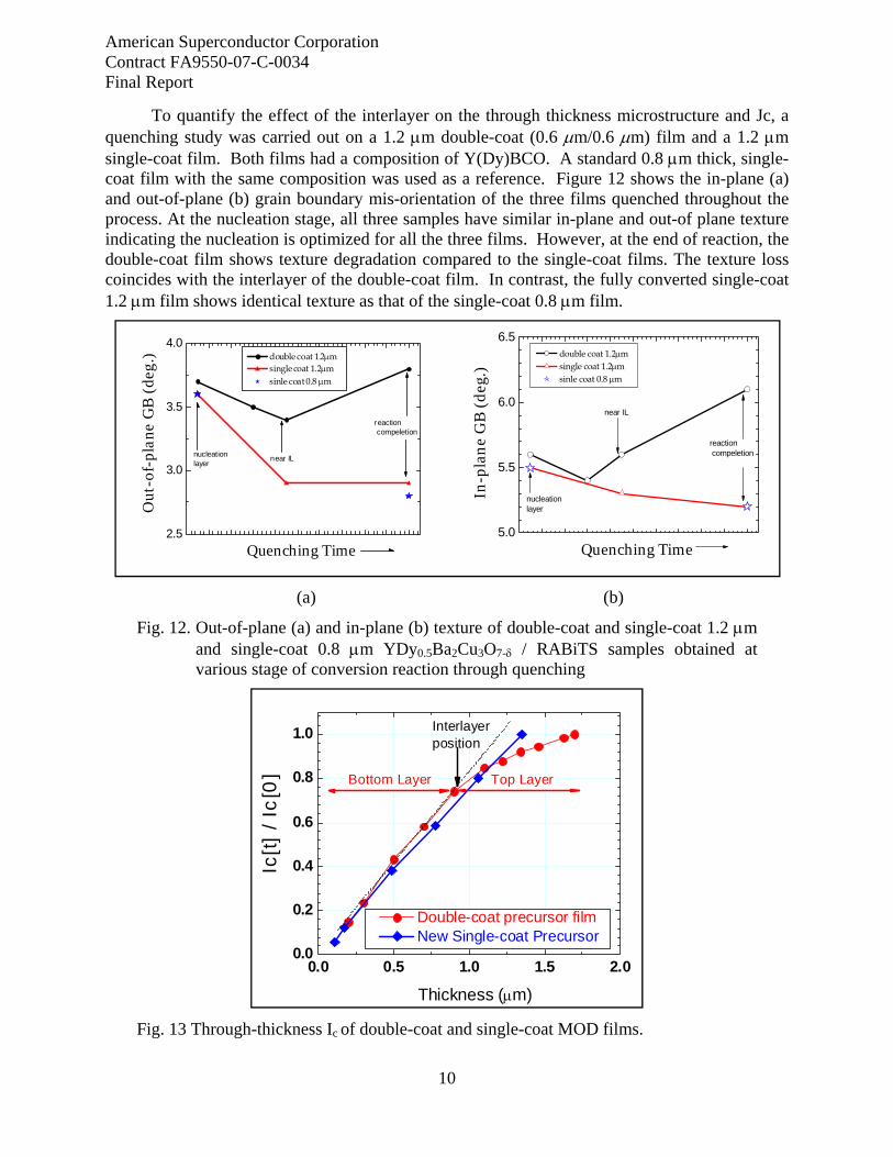
To quantify the effect of the interlayer on the through thickness microstructure and Jc, a quenching study was carried out on a 1.2 μm double-coat (0.6 μm/0.6 μm) film and a 1.2 μm single-coat film. Both films had a composition of Y(Dy)BCO. A standard 0.8 μm thick, single-coat film with the same composition was used as a reference. Figure 12 shows the in-plane (a) and out-of-plane (b) grain boundary mis-orientation of the three films quenched throughout the process. At the nucleation stage, all three samples have similar in-plane and out-of plane texture indicating the nucleation is optimized for all the three films. However, at the end of reaction, the double-coat film shows texture degradation compared to the single-coat films. The texture loss coincides with the interlayer of the double-coat film. In contrast, the fully converted single-coat 1.2 μm film shows identical texture as that of the single-coat 0.8 μm film.
(a) (b)
Fig. 12. Out-of-plane (a) and in-plane (b) texture of double-coat and single-coat 1.2 μm and single-coat 0.8 μm YDy0.5Ba2Cu3O7-δ / RABiTS samples obtained at various stage of conversion reaction through quenching
Fig. 13 Through-thickness Ic of double-coat and single-coat MOD films.
2.5
3.0
3.5
4.0 double coat 1.2μm single coat 1.2μm sinle coat 0.8 μm
Out
-of-
plan
e G
B (
deg.
)
Quenching Time
near IL
nucleationlayer
reaction compeletion
5.0
5.5
6.0
6.5 double coat 1.2μm single coat 1.2μm sinle coat 0.8 μm
near IL
In-p
lan
e G
B (
deg
.)
Quenching Time
nucleationlayer
reaction compeletion
0.0 0.5 1.0 1.5 2.00.0
0.2
0.4
0.6
0.8
1.0
Top Layer
Double-coat precursor film New Single-coat Precursor
Ic [t
] / I
c[0
]
Thickness (μm)
Interlayerposition
Bottom Layer

American Superconductor Corporation Contract FA9550-07-C-0034 Final Report
11
Through thickness Jc measurements, shown in Figure 13, confirmed a constant through thickness Jc in the single-coat film. This is consistent with the uniform through microstructure seen in the cross-sectional TEM image in Figure 14. In contrast, the multi-coat film shows a decrease in Jc above the interlayer boundary. This result clearly shows that the thick film reaction process developed during the Phase II program is capable of processing thick MOD films with constant through thickness Jc.
Fig. 14. Cross-sectional TEM micrograph of a fully processes 1.2 μm single-coat
Y(Dy(123) film. A uniform density of nanoparticles and stacking faults are seen throughout the film thickness.
Using the optimized reaction process for thick MOD film developed during the Phase II program, we achieved a critical current of 440 A/cm-w (77K, self-field) with a single-coat 1.2 μm film. As shown in Figure 15, the single-coat MOD films maintain a nearly constant Jc of ~ 3.5 MA/cm2 independent of thickness. This new thick film will be transferred to AMSC’s manufacturing line in the coming year.
Fig. 15. Ic vs. thickness for single coat Metal Organic-based YBCO precursors.
0.0 0.5 1.00
100
200
300
400
500
0
50
100
150
200
Ic (A
/cm
-w)
Y(Dy)BCO Thickness (μm)
Equ
ival
ent 3
44 S
uper
cond
ucto
r Ic
(A)

American Superconductor Corporation Contract FA9550-07-C-0034 Final Report
12
The Jc through thickness degradation in double coat and triple coat films is caused by the formation of a Cu-rich interlayer that blocks the continuous epitaxial through thickness YBCO growth. A separate effort to eliminate the Cu-rich interlayer in the multi-layer precursor film was initiated by collaborators at Oak Ridge and Argonne National Laboratories. This separate effort has achieved a critical current of 660 A/cm-w in a triple coat-film (2.0 μm) with the architecture of Y123-0.6μm/ Y123-0.6μm/Y(Dy)123-0.8μm (top to bottom) [9].
Task 2. Continuous Coating and Decomposition Development for Thick Film Precursors Multi-Coat Precursors
The Phase I program demonstrated the technical viability of preparing the thick YBCO films using a multi-step coating/decomposition process. However, the Phase I program was limited to preparing the multi-coat films in lengths of 1 – 2 meters, using the R&D coating and decomposition equipment. During Phase II program, the coating and decomposition process for the double coat, 1.4 μm thick YBCO films was transferred to AMSC’s pilot manufacturing line and successfully used for preparing multiple 100 meter lengths of 1.4 μm YBCO films on 40-mm wide RABiTS templates. The work during the Phase II project focused on adjusting the decomposition line speeds and process gas composition (O2 and H2O) for each of the individual layers to prevent the formation of cracks and blisters during either of the two decomposition steps and to prevent delamination of the layers.
Detailed examination of the double-coat films, coated in lengths up to ~100 meters showed no increase in defect density compared to the standard, single-coat films. In addition, there was no evidence of delamination between the two layers.
The 1.4 μm HTS films were prepared by initially slot die coating and decomposing an 0.8 μm thick Y(Dy)BCO layer and then coating and decomposing a 0.6 μm thick YBCO layer. This double coat, hybrid film architecture was used for long length processing throughout the Phase II program. The triple-coat (2.0 μm total thickness) films were prepared by coating and decomposition a third 0.6 μm thick YBCO layer.
Single-Coat Precursors
During Phase II program, experiments were carried out to optimize the process gas composition, flow dynamics and temperature profile of precursor decomposition process in the production equipment. These process modifications allowed the development of a modified decomposition process for the RE-doped YBCO precursor that that resulted in an increase in the maximum single-coat thickness to 1.2 μm – a 50% increase from the 0.8 μm baseline thickness. The single coat films have a uniform through thickness microstructure and composition as shown in Figure 16.
Y(Dy)BCO films of 1.4 μm were also prepared; however, these samples exhibited occasional defects during the decomposition stage. These 1.2 μm thick films were also used in the multi-coat process to prepare samples with total thickness of 2.0 μm.

American Superconductor Corporation Contract FA9550-07-C-0034 Final Report
13
Fig. 16. Single-coat Y(Dy)BCO precursor film after decomposition: (a) STEM (BF)
cross-section image and (b) elemental maps showing through thickness distribution. Thickness is equivalent to a fully processed 1.2 μm YBCO film.
Task 3. Continuous Reaction Development for Thick YBCO Films This task focused on transferring the reaction process developed for the short samples to
continuous lengths of 40 mm wide tape in AMSC’s pilot-scale roll-to-roll reaction furnace. The precursor used for the continuous processing consisted of the hybrid double-coat, 1.4 μm films comprised of a 0.8 μm thick bottom layer of rare earth doped (Y(Dy)BCO and a 0.6 μm top layer of YBCO.
The pilot HTS reaction equipment at AMSC, is shown in Fig. 17. The roll-to-roll furnace consists of multiple temperature zones that correspond to the S1 through S4 zones described in Task 1 for the moving short sample furnace and processing. The temperature ramp rates and process times are controlled by varying the temperature profile of the furnace and/or varying the speed that the strip is transported through the furnace. Process optimization was carried using a design of experiment approach out as a function of p[H2O], p[O2], temperature and line speed (ramp rate or residence time) in each of the individual furnace zones. Development of the thick film processing was carried out using tapes with lengths < 5 meters.
Fig. 17. Pilot scale reaction furnace used for the roll-to-roll processing the continuous
lengths of 40 mm wide strips with a 1.4 μm thick HTS layer
The reaction process for the hybrid 1.4 μm thick YBCO films on 40 mm wide production RABiTS templates was successfully transferred to AMSC’s pilot manufacturing line. Under optimized process conditions, critical currents of over 450A/cm-w (77K, self-field) were reproducibly obtained with multiple test runs. This is slightly below the maximum critical

American Superconductor Corporation Contract FA9550-07-C-0034 Final Report
14
current of 50A/cm-w obtained with the same thickness, double-coat films on short samples in the R&D equipment.
As expected, processing of thicker HTS layers required longer reaction time. During the Phase II program, it was established that the maximum thickness film that could be processed in the pilot roll-to-roll manufacturing furnace was ~1.5 μm. Additional increase in thickness requires increasing the length of the furnace in order to maintain the required ramp and reaction times. Although films up to 2 μm were successfully processed in short in the short length R&D equipment, it was not possible to transfer this process to the roll-to-roll reaction furnace. A new furnace was designed and ordered to accommodate the thicker films; however, it was not delivered before the completion of the Phase II project.
Task 4. Manufacture and Characterization of High Critical Current 344 Superconductor Wires
One hundred meter lengths of 2G wire with a 1.4 μm HTS layer were processed in AMSC’s roll-to-roll manufacturing line during the Phase II program. The precursor film consisted of the hybrid architecture consisting of an 0.8 μm Y(Dy)BCO layer on bottom and an 0.6 μm YBCO layer on top. The layers were deposited on a 40 mm wide RABiTS template using a slot die coating technique and decomposition process developed in Task 2. The HTS processing parameters were selected based on the results obtained in the Task 3. After reaction, the 40-mm web was coated on both sides with a silver layer then slit into eight 4-mm width tapes which were laminated between to two copper strips.
A number of 100 meter length strips, with the hybrid, 1.4 μm HTS layer, were processed during the Phase II project. Figure 18 shows the Ic measured (1 meter tap length) along the length of a typical 344 superconductor wire. The wire had an average Ic of 145 A (362 A/cm-w) with sections ranging over 170 A (425 A/cm-w). Although there was a periodic variation in Ic along the length, short lengths of the wire had very consistent Ic as shown for a 6 meter section in Fig. 19.
Fig. 18. Critical current along the length of a 94 meter long 344 superconductor wire
with a 1.4 μm thick HTS layer (Ic was measured at 1 meter tap length).

American Superconductor Corporation Contract FA9550-07-C-0034 Final Report
15
Fig. 19. Critical current along the length of a 6-meter long 344 superconductor wire
with a 1.4 μm thick YBCO layer (Ic was measured at 1 meter tap length).
Fig 20 shows the average Ic measured over the length of eight 344 superconductor wires cut from a single 40 mm strip. The variation in the average Ic between even and odd slits is due to a small Ic degradation due to the configuration of the slitting knives.
Fig. 20. Average Ic measured along the length of each of the eight 344 superconductor
wires cut from a single 40 mm strip (Ic was measured at 1 meter tap length).
344 superconductors prepared with the 1.4 μm HTS layer were used to fabricate a solenoid coil. The coil, shown in Fig. 21 was constructed from 12 pancake coils and used 420 meters of wire. The coil ID and OD were 5 cm and 12 cm respectively. The coil generated a 1T field at 73K and 1.5 T at ~65 K as shown in Fig. 22.
.
0
25
50
75
100
125
150
175
200
0
100
200
300
400
500
Wire
Crit
ical
Cur
rent
(A)
Position (meter)2 3 4 51
77K, self-field I c/w
idth
(A/c
m-w
idth
of i
nser
t)
344 superconductors with 1.4 μm Y(Dy)BCO

American Superconductor Corporation Contract FA9550-07-C-0034 Final Report
16
Fig. 21. 2G coil prepared with 420 m of 2G wire made with the 1.4 μm hybrid HTS layer.
Fig. 22. Magnetic field generated in the center of the 5-cm ID 2G coil as a function of
operating temperature.
SUMMARY During this Phase I and Phase II program, we successfully developed and optimized key
processing parameters for obtaining high critical currents in thick MOD-based YBCO films and successfully demonstrated the thick film process in AMSC’s roll-to-roll pilot manufacturing line. Multiple 100 meters lengths of 344 superconductor wires were manufacture using the thick film process developed in this project. The 344 wires achieved end-to-end critical currents exceeding 300 A/cm-w (77K, self-field). These were the first long length 2G wires to achieve this milestone.
The Phase II project was also successful in demonstrating a modified roll-to-roll decomposition procedure for the MOD-based YBCO films that resulted in a 50% increase in the single-coat thickness to 1.2 μm.

American Superconductor Corporation Contract FA9550-07-C-0034 Final Report
17
The fundamental understanding and key learning obtained during Phase I and Phase II programs has lead to significant improvements in the long length manufacturing of 2G wires at AMSC. 344 superconductor wires with an 0.8 μm thick Y(Dy)BCO films are now achieving critical currents exceeding 250 A/cm-w (77K, self-field). The knowledge gained from this project has also been used in designing the next generation of roll-to-roll equipment for processing the thick YBCO films.
REFERENCES
1. D. Larbalestier, A. Gurevich, D. M. Feldmann and A. Polyanskii, Nature 414, 368-377 (2001).
2 S. R. Foltyn, P. Tiwari, R. C. Dye, M. Q. Le and X. D. Wu, Applied Physics Letters 63, 1848-1850 (1993).
3 X. D. Wu, S. R. Foltyn, P. Arendt, J. Townsend, I. H. Campbell, P. Tiwari, Q. X. Jia, J. O. Willis, M. P. Maley, J. Y. Coulter and D. E. Peterson, IEEE Transactions on Applied Superconductivity 5, 2001-2006 (1995).
4 S. R. Foltyn, Q. X. Jia, P. N. Arendt, L. Kinder, Y. Fan and J. F. Smith, Applied Physics Letters 75, 3692-3694 (1999).
5 J. R. Groves, P. N. Arendt, S. R. Foltyn, Q. X. Jia, T. G. Holesinger, H. Kung, E. J. Peterson, R. F. DePaula, P. C. Dowden, L. Stan and L. A. Emmert, Journal of Materials Research Society, 16, 2175-2178 (2001).
6 B. W. Kang, A. Goyal, D. R. Lee, J. E. Mathis, E. D. Specht, P. M. Martin, D. M. Kroeger, M. Paranthaman and S. Sathyamurthy, Journal of Materials Research Society, 17, 1750-1757 (2002)
7 V. F. Solovyov, H. J. Wiesmann, L. J. Wu, M. Suenaga and R. Feenstra, IEEE Transactions on Applied Superconductivity, 9, 1467-1470 (1999).
8. J. A. Smith, M. J. Cima and N. Sonnenberg, IEEE Transactions on Applied Superconductivity, 9, 1531-1534 (1999).
9 M.W. Rupich, D. Miller, R. Feenstra and T.G. Holesinger, , Wire Development Group Presentation, 2009 DOE Peer Review, (Alexandria VA, Aug. 2009) http://www.htspeerreview.com/pdfs/presentations/day%201/joint/3-Joint-Wire-Development-Group.pdf