cse477 vlsi digital circuits fall 2002 lecture 20: adder ... · mirror adder features ......
TRANSCRIPT
CSE477 L20 Adder Design.1 Irwin&Vijay, PSU, 2002
CSE477VLSI Digital Circuits
Fall 2002
Lecture 20: Adder Design
Mary Jane Irwin ( www.cse.psu.edu/~mji ) www.cse.psu.edu/~cg477
[Adapted from Rabaey’s Digital Integrated Circuits, ©2002, J. Rabaey et al.]
CSE477 L20 Adder Design.2 Irwin&Vijay, PSU, 2002
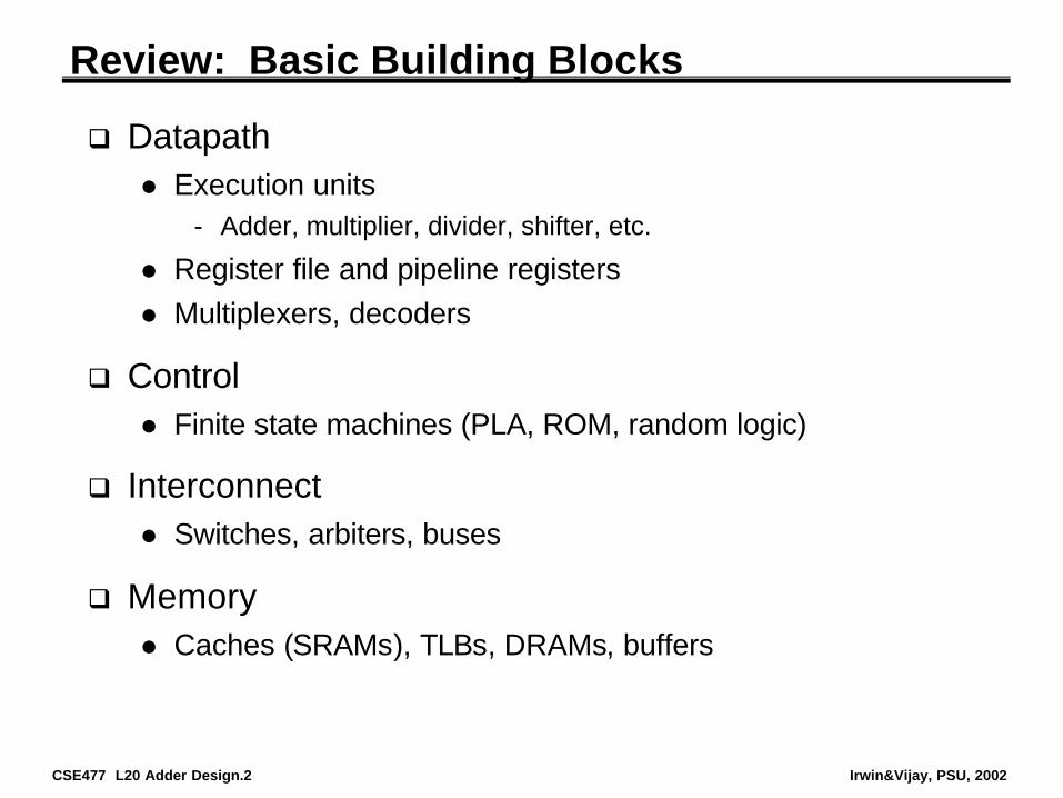
Review: Basic Building Blocks
q Datapathl Execution units
- Adder, multiplier, divider, shifter, etc.
l Register file and pipeline registersl Multiplexers, decoders
q Controll Finite state machines (PLA, ROM, random logic)
q Interconnectl Switches, arbiters, buses
q Memoryl Caches (SRAMs), TLBs, DRAMs, buffers

CSE477 L20 Adder Design.3 Irwin&Vijay, PSU, 2002
The 1-bit Binary Adder
1-bit Full Adder(FA)
A
BS
Cin
S = A ⊕ B ⊕ Cin
Cout = A&B | A&Cin | B&Cin (majority function)
q How can we use it to build a 64-bit adder?
q How can we modify it easily to build an adder/subtractor?
q How can we make it better (faster, lower power, smaller)?
generate
generate
propagate
propagate
propagate
propagate
kill
kill
carry status
11111
01011
01101
10001
01110
10010
10100
00000
SCoutCinBA
Cout
G = A&BP = A ⊕ BK = !A & !B
= P ⊕ Cin
= G | P&Cin
CSE477 L20 Adder Design.4 Irwin&Vijay, PSU, 2002
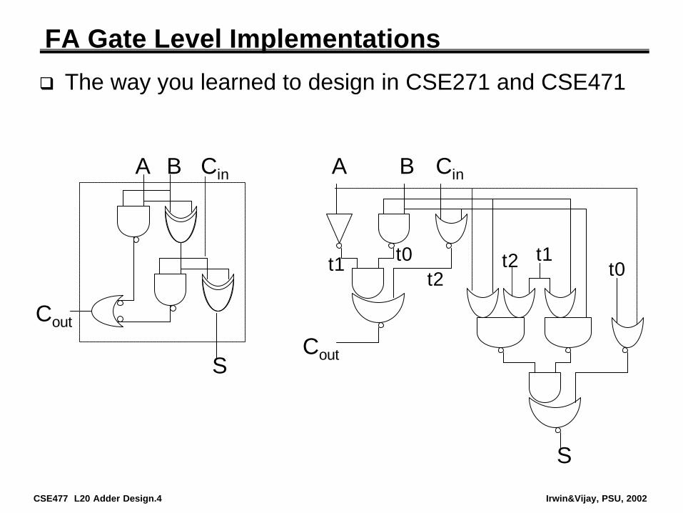
FA Gate Level Implementations
A B
S
Cout
Cin
t1 t0t2 t0
t1
A B
S
Cout
Cin
t2
q The way you learned to design in CSE271 and CSE471
CSE477 L20 Adder Design.5 Irwin&Vijay, PSU, 2002
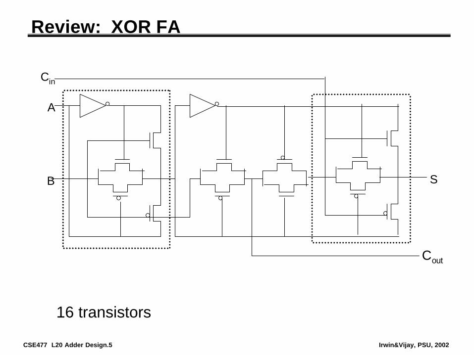
Review: XOR FA
Cout
S
Cin
A
B
16 transistors

CSE477 L20 Adder Design.6 Irwin&Vijay, PSU, 2002
Review: CPL FA
A
!A
B!B Cin!Cin
!S
S
Cout
!CoutA
!A
B
!B
!B
B Cin !Cin
Cin
!Cin
20+8 transistors, dual rail – beware of threshold drops
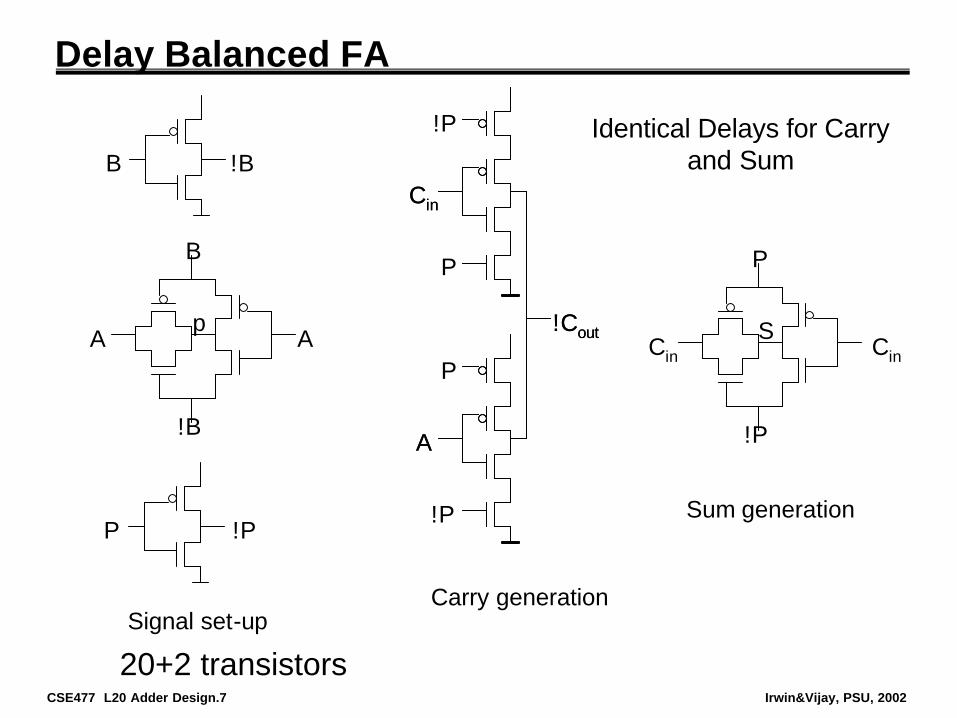
CSE477 L20 Adder Design.7 Irwin&Vijay, PSU, 2002
Delay Balanced FA
B !BIdentical Delays for Carry
and Sum
P !P
Signal set-up
B
A
!B
pA
Carry generation
Sum generation
Cin
!P
A
!Cout
!P
P
Cin
P
A
!Cout
P
!P
SCin Cin
20+2 transistors
CSE477 L20 Adder Design.8 Irwin&Vijay, PSU, 2002
Review: Mirror Adder
B
B B
B B
B
B
BA
A
A
A
A
A A
A
Cin
Cin
Cin
Cin
Cin!Cout !S
24+4 transistors
kill
generate
0-propagate
1-propagate
Cout = A&B | B&Cin | A&Cin SUM = A&B&Cin | COUT&(A | B | Cin)
4 4
4 4
4
8
888
8
2 2 23
3
3
6
6
6
444
4
2
Sizing: Each input in the carry circuit has a logical effort of 2 so the optimal fan-out for each is also 2. Since !Cout drives 2 internal and 2 inverter transistor gates (to form Cin for the nms bit adder) should oversize the carry circuit. PMOS/NMOS ratio of 2.

CSE477 L20 Adder Design.9 Irwin&Vijay, PSU, 2002
Mirror Adder Featuresq The NMOS and PMOS chains are completely
symmetrical with a maximum of two series transistors in the carry circuitry, guaranteeing identical rise and fall transitions if the NMOS and PMOS devices are properly sized.
q When laying out the cell, the most critical issue is the minimization of the capacitances at node !Cout (four diffusion capacitances, two internal gate capacitances, and two inverter gate capacitances). Shared diffusions can reduce the stack node capacitances.
q The transistors connected to Cin are placed closest to the output.
q Only the transistors in the carry stage have to be optimized for optimal speed. All transistors in the sum stage can be minimal size.
CSE477 L20 Adder Design.10 Irwin&Vijay, PSU, 2002
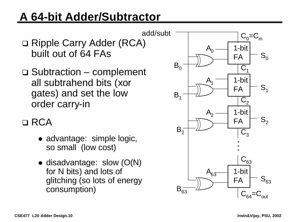
A 64-bit Adder/Subtractor
1-bit FA S0
C0=Cin
C1
1-bit FA S1
C2
1-bit FA S2
C3
C64=Cout
1-bit FA S63
C63
. . .
q Ripple Carry Adder (RCA) built out of 64 FAs
q Subtraction – complement all subtrahend bits (xorgates) and set the low order carry-in
q RCA
l advantage: simple logic, so small (low cost)
l disadvantage: slow (O(N) for N bits) and lots of glitching (so lots of energy consumption)
A0
B0
A1
B1
A2
B2
A63
B63
add/subt
CSE477 L20 Adder Design.11 Irwin&Vijay, PSU, 2002
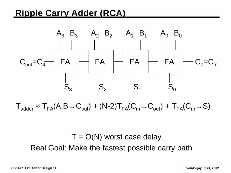
Ripple Carry Adder (RCA)
A0 B0
S0
C0=CinFA
A1 B1
S1
FA
A2 B2
S2
FA
A3 B3
S3
FACout=C4
T = O(N) worst case delay
Tadder ≈ TFA(A,B→Cout) + (N-2)TFA(Cin→Cout) + TFA(Cin→S)
Real Goal: Make the fastest possible carry path
CSE477 L20 Adder Design.12 Irwin&Vijay, PSU, 2002
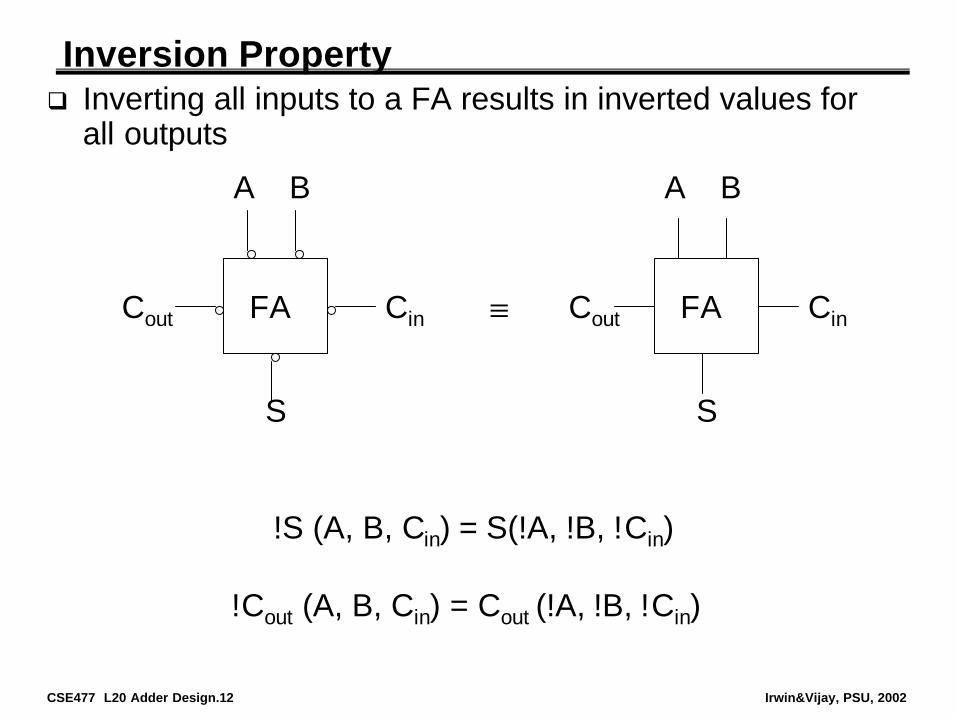
Inversion Property
A B
S
CinFA
!Cout (A, B, Cin) = Cout (!A, !B, !Cin)
Cout
A B
S
FACout Cin
!S (A, B, Cin) = S(!A, !B, !Cin)
≡
q Inverting all inputs to a FA results in inverted values for all outputs

CSE477 L20 Adder Design.13 Irwin&Vijay, PSU, 2002
Exploiting the Inversion Property
A0 B0
S0
C0=CinFA’
A1 B1
S1
FA’
A2 B2
S2
FA’
A3 B3
S3
FA’Cout=C4
Now need two “flavors” of FAs
regular cellinverted cell
q Minimizes the critical path (the carry chain) by eliminating inverters between the FAs (will need to increase the transistor sizing on the carry chain portion of the mirror adder).
CSE477 L20 Adder Design.14 Irwin&Vijay, PSU, 2002
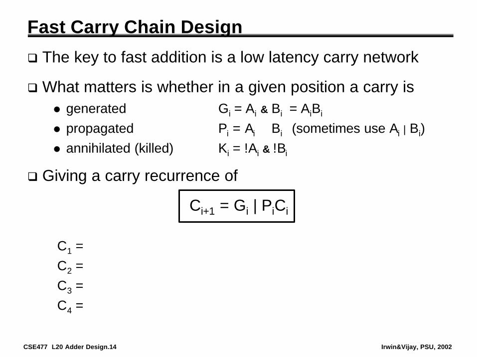
Fast Carry Chain Design
q The key to fast addition is a low latency carry network
q What matters is whether in a given position a carry isl generated Gi = Ai & Bi = AiBi
l propagated Pi = Ai ⊕ Bi (sometimes use Ai | Bi)l annihilated (killed) Ki = !Ai & !Bi
q Giving a carry recurrence of
Ci+1 = Gi | PiCi
C1 =C2 = C3 =C4 =
CSE477 L20 Adder Design.15 Irwin&Vijay, PSU, 2002
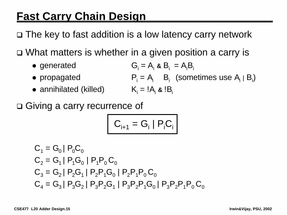
Fast Carry Chain Design
q The key to fast addition is a low latency carry network
q What matters is whether in a given position a carry isl generated Gi = Ai & Bi = AiBi
l propagated Pi = Ai ⊕ Bi (sometimes use Ai | Bi)l annihilated (killed) Ki = !Ai & !Bi
q Giving a carry recurrence of
Ci+1 = Gi | PiCi
C1 = G0 | P0C0
C2 = G1 | P1G0 | P1P0 C0
C3 = G2 | P2G1 | P2P1G0 | P2P1P0 C0
C4 = G3 | P3G2 | P3P2G1 | P3P2P1G0 | P3P2P1P0 C0

CSE477 L20 Adder Design.16 Irwin&Vijay, PSU, 2002
Manchester Carry Chain
q Switches controlled by Gi and Pi
q Total delay ofl time to form the switch control signals Gi and Pi
l setup time for the switchesl signal propagation delay through N switches in the worst case
Gi Pi
!Ci!Ci+1
clk

CSE477 L20 Adder Design.17 Irwin&Vijay, PSU, 2002
4-bit Sliced MCC Adder
G P
!C0
clk
G PG PG P
⊕⊕⊕⊕
& ⊕& ⊕& ⊕& ⊕
A0 B0A1 B1A2 B2A3 B3
S0S1S2S3
!C1!C2!C3
!C4
CSE477 L20 Adder Design.18 Irwin&Vijay, PSU, 2002
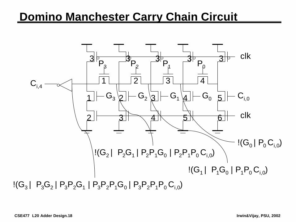
Domino Manchester Carry Chain Circuit
Ci,0G0
clk
clkP0P1P2P3
G1G2G3
Ci,41 2 3 4
5
6
3 3 3 3 3
1
2
2
3
3
4
4
5
!(G0 | P0 Ci,0)
!(G1 | P1G0 | P1P0 Ci,0)
!(G2 | P2G1 | P2P1G0 | P2P1P0 Ci,0)
!(G3 | P3G2 | P3P2G1 | P3P2P1G0 | P3P2P1P0 Ci,0)
CSE477 L20 Adder Design.19 Irwin&Vijay, PSU, 2002
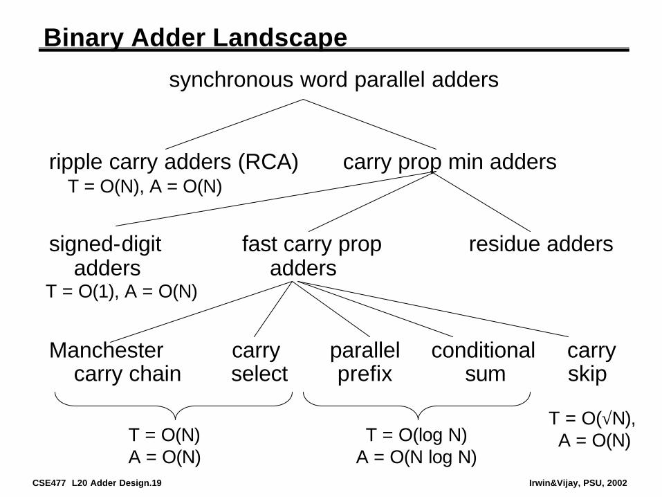
Binary Adder Landscape
synchronous word parallel adders
ripple carry adders (RCA) carry prop min adders
signed-digit fast carry prop residue adders adders adders
Manchester carry parallel conditional carry carry chain select prefix sum skip
T = O(N), A = O(N)
T = O(1), A = O(N)
T = O(log N)A = O(N log N)
T = O(√N), A = O(N)T = O(N)
A = O(N)

CSE477 L20 Adder Design.20 Irwin&Vijay, PSU, 2002
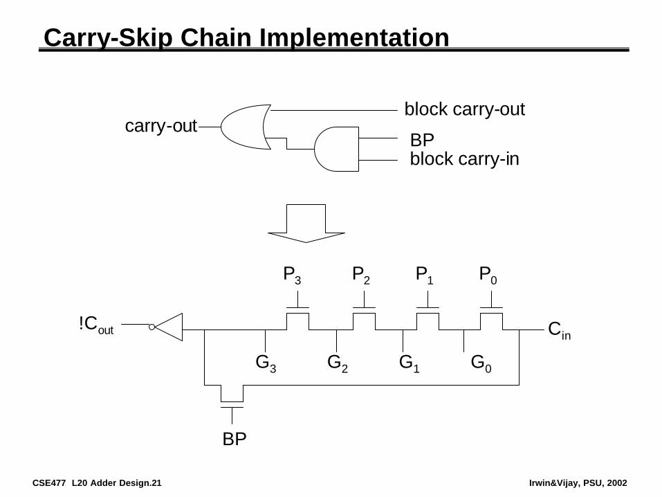
Carry-Skip (Carry-Bypass) Adder
If (P0 & P1 & P2 & P3 = 1) then Co,3 = Ci,0 otherwise the block itself kills or generates the carry internally
A0 B0
S0
Ci,0FA
A1 B1
S1
FA
A2 B2
S2
FA
A3 B3
S3
FACo,3
Co,3
BP = P0 P1 P2 P3 “Block Propagate”
CSE477 L20 Adder Design.21 Irwin&Vijay, PSU, 2002
Carry-Skip Chain Implementation
BPblock carry-in
block carry-outcarry-out
Cin
G0
P0P1P2P3
G1G2G3
!Cout
BP
CSE477 L20 Adder Design.22 Irwin&Vijay, PSU, 2002
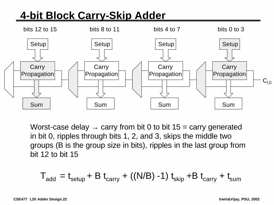
4-bit Block Carry-Skip Adder
Worst-case delay → carry from bit 0 to bit 15 = carry generated in bit 0, ripples through bits 1, 2, and 3, skips the middle two groups (B is the group size in bits), ripples in the last group from bit 12 to bit 15
Ci,0
Sum
CarryPropagation
Setup
Sum
CarryPropagation
Setup
Sum
CarryPropagation
Setup
Sum
CarryPropagation
Setup
bits 0 to 3bits 4 to 7bits 8 to 11bits 12 to 15
Tadd = tsetup + B tcarry + ((N/B) -1) tskip +B tcarry + tsum
CSE477 L20 Adder Design.23 Irwin&Vijay, PSU, 2002
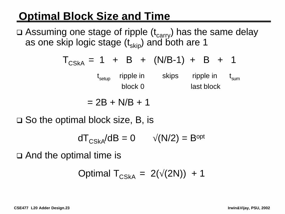
Optimal Block Size and Timeq Assuming one stage of ripple (tcarry) has the same delay
as one skip logic stage (tskip) and both are 1
TCSkA = 1 + B + (N/B-1) + B + 1
tsetup ripple in skips ripple in tsum
block 0 last block
= 2B + N/B + 1
q So the optimal block size, B, is
dTCSkA/dB = 0 ⇒ √(N/2) = Bopt
q And the optimal time is
Optimal TCSkA = 2(√(2N)) + 1
CSE477 L20 Adder Design.24 Irwin&Vijay, PSU, 2002
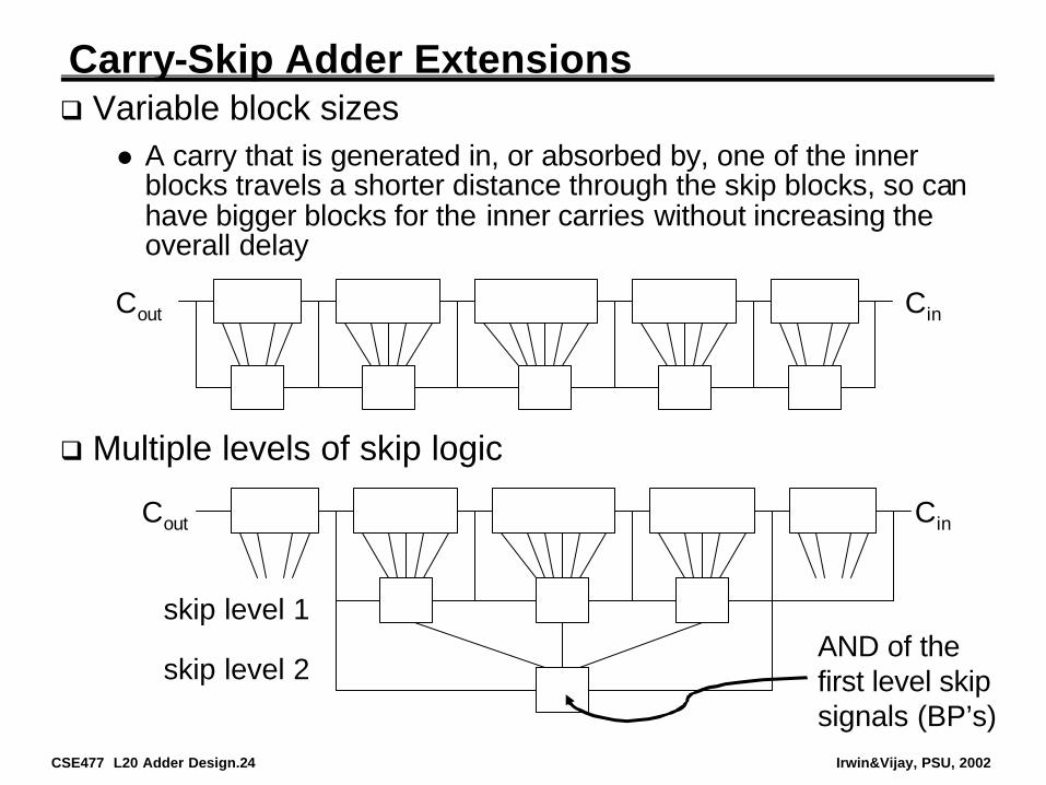
Carry-Skip Adder Extensionsq Variable block sizes
l A carry that is generated in, or absorbed by, one of the inner blocks travels a shorter distance through the skip blocks, so can have bigger blocks for the inner carries without increasing the overall delay
CinCout
q Multiple levels of skip logic
skip level 1
skip level 2
CinCout
AND of the first level skip signals (BP’s)
CSE477 L20 Adder Design.25 Irwin&Vijay, PSU, 2002
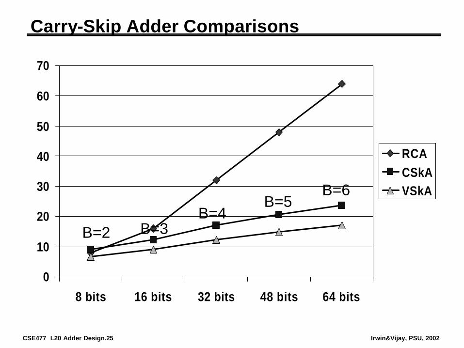
Carry-Skip Adder Comparisons
0
10
20
30
40
50
60
70
8 bits 16 bits 32 bits 48 bits 64 bits
RCACSkAVSkA
B=2 B=3B=4
B=5B=6

CSE477 L20 Adder Design.26 Irwin&Vijay, PSU, 2002
Carry Select Adder
4-b Setup
“0” carry propagation
“1” carry propagation 1
0
multiplexer CinCout
Sum generation
P’s G’s
C’s
q Precompute the carry out of each block for both carry_in = 0 and carry_in = 1 (can be done for all blocks in parallel) and then select the correct one
A’s B’s
S’s
CSE477 L20 Adder Design.27 Irwin&Vijay, PSU, 2002
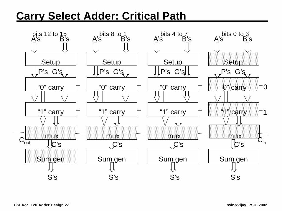
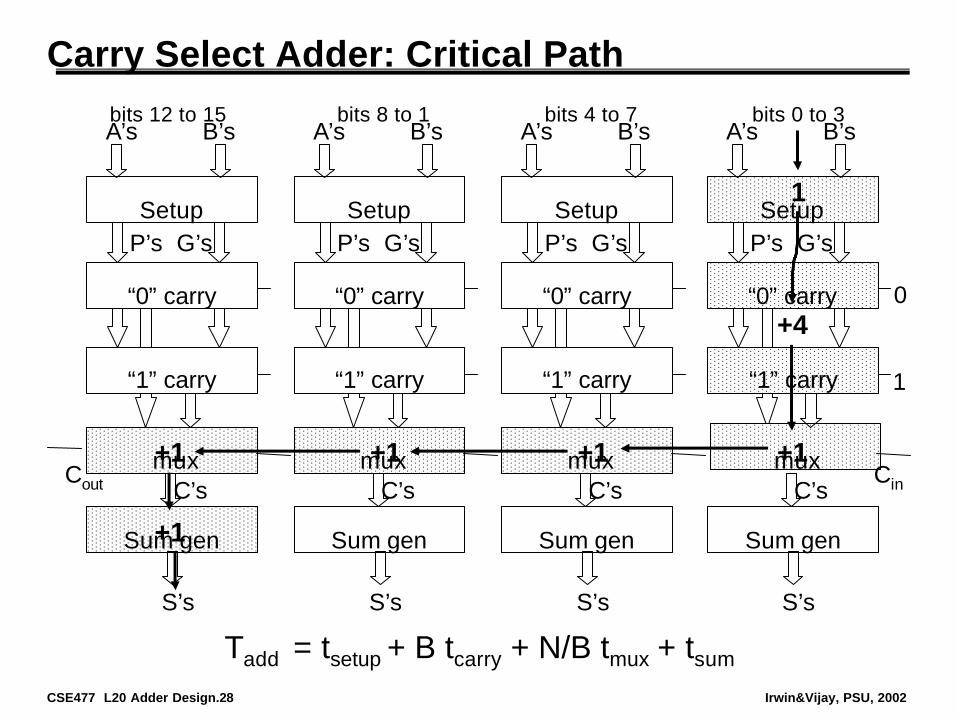
Carry Select Adder: Critical Path
Setup
“0” carry
“1” carry 1
0
mux Cin
Sum gen
P’s G’s
C’s
S’s
A’s B’s
Setup
“0” carry
“1” carry
mux
Sum gen
P’s G’s
C’s
S’s
A’s B’s
Setup
“0” carry
“1” carry
mux
Sum gen
P’s G’s
C’s
S’s
A’s B’s
Setup
“0” carry
“1” carry
muxCout
Sum gen
P’s G’s
C’s
S’s
A’s B’sbits 0 to 3bits 4 to 7bits 8 to 1bits 12 to 15
CSE477 L20 Adder Design.28 Irwin&Vijay, PSU, 2002
Carry Select Adder: Critical Path
Setup
“0” carry
“1” carry 1
0
mux Cin
Sum gen
P’s G’s
C’s
S’s
A’s B’s
Setup
“0” carry
“1” carry
mux
Sum gen
P’s G’s
C’s
S’s
A’s B’s
Setup
“0” carry
“1” carry
mux
Sum gen
P’s G’s
C’s
S’s
A’s B’s
Setup
“0” carry
“1” carry
muxCout
Sum gen
P’s G’s
C’s
S’s
A’s B’sbits 0 to 3bits 4 to 7bits 8 to 1bits 12 to 15
Tadd = tsetup + B tcarry + N/B tmux + tsum
1
+4
+1+1+1+1
+1

CSE477 L20 Adder Design.29 Irwin&Vijay, PSU, 2002
Square Root Carry Select Adder
Setup
“0” carry
“1” carry 1
0
mux Cin
Sum gen
P’sG’s
C’s
S’s
A’s B’sA’s B’s
S’s
Setup
“0” carry
“1” carry
mux
Sum gen
P’s G’s
C’s
A’s B’s
Setup
“0” carry
“1” carry
muxCout
Sum gen
P’s G’s
C’s
S’s
A’s B’sbits 0 to 1bits 2 to 4bits 5 to 8bits 9 to 13
Setup
mux
Sum gen
P’s G’s
C’s
S’s
“1” carry
“0” carry
Setup
“0” carry
“1” carry
mux
Sum gen
P’s G’s
C’s
A’s B’sbits 14 to 19
S’s
CSE477 L20 Adder Design.30 Irwin&Vijay, PSU, 2002
Square Root Carry Select Adder
Setup
“0” carry
“1” carry 1
0
mux Cin
Sum gen
P’sG’s
C’s
S’s
As B’sA’s Bs
1
0
S’s
Setup
“0” carry
“1” carry
mux
Sum gen
P’s G’s
C’s
A’s B’s
Setup
“0” carry
“1” carry 1
0
muxCout
Sum gen
P’s G’s
C’s
S’s
A’s B’sbits 0 to 1bits 2 to 4bits 5 to 8bits 9 to 13
Tadd = tsetup + 2 tcarry + vN tmux + tsum
Setup
1
0
mux
Sum gen
P’s G’s
C’s
S’s
“1” carry
“0” carry
Setup
“0” carry
“1” carry
mux
Sum gen
P’s G’s
C’s
A’s B’sbits 14 to 19
1
+2
+1+1+1+1+1
+1
+3+4+5+6
S’s
CSE477 L20 Adder Design.31 Irwin&Vijay, PSU, 2002
Parallel Prefix Adders (PPAs)q Define carry operator € on (G,P) signal pairs
l € is associative, i.e.,[(g’’’,p’’’) € (g’’,p’’)] € (g’,p’) = (g’’’,p’’’) € [(g’’,p’’) € (g’,p’)]
€
(G’’,P’’) (G’,P’)
(G,P)
whereG = G’’ ∨ P’’G’P = P’’P’
€
€ €
€
G’
!G
G’’
P’’

CSE477 L20 Adder Design.32 Irwin&Vijay, PSU, 2002
PPA General Structureq Given P and G terms for each bit position, computing all
the carries is equal to finding all the prefixes in parallel
(G0,P0) € (G1,P1) € (G2,P2) € … € (GN-2,PN-2) € (GN-1,PN-1)
q Since € is associative, we can group them in any order l but note that it is not commutative
q Measures to considerl number of € cellsl tree cell depth (time)l tree cell areal cell fan-in and fan-outl max wiring lengthl wiring congestionl delay path variation (glitching)
Pi, Gi logic (1 unit delay)
Si logic (1 unit delay)
Ci parallel prefix logic tree (1 unit delay per level)
CSE477 L20 Adder Design.33 Irwin&Vijay, PSU, 2002
Brent-Kung PPAP
aral
lel P
refix
Com
puta
tion
€
G0P0
G1P1
G2p2
G3P3
G4P4
G5P5
G6P6
G7P7
G8P8
G9p9
G10P10
G11p11
G12P12
G13p13
G14p14
G15p15
€€€€€€€
€ € € €
€
€
€
€
€
€
€ € € € € €
€ €
C1C2C3C4C5C6C7C8C9C10C11C12C13C14C15C16
Cin
€
T =
log 2N
T =
log 2N
-2
A =
2lo
g 2N
A = N/2
CSE477 L20 Adder Design.34 Irwin&Vijay, PSU, 2002
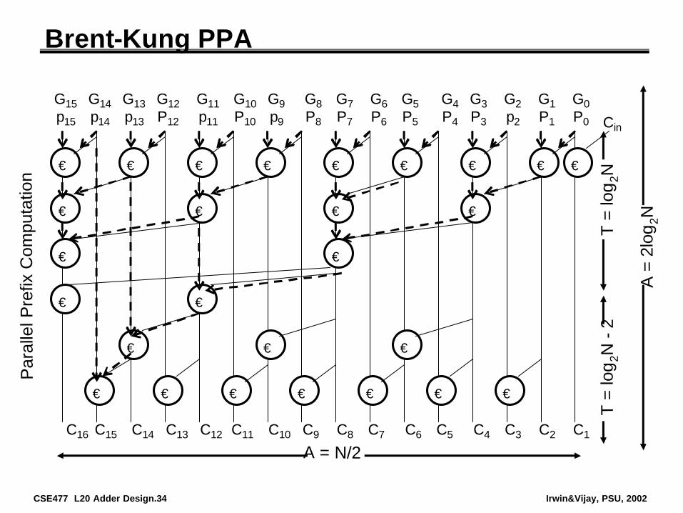
Brent-Kung PPAP
aral
lel P
refix
Com
puta
tion
€
G0P0
G1P1
G2p2
G3P3
G4P4
G5P5
G6P6
G7P7
G8P8
G9p9
G10P10
G11p11
G12P12
G13p13
G14p14
G15p15
€€€€€€€
€ € € €
€
€
€
€
€
€
€ € € € € €
€ €
C1C2C3C4C5C6C7C8C9C10C11C12C13C14C15C16
Cin
€
T =
log 2N
T =
log 2N
-2
A =
2lo
g 2N
A = N/2
CSE477 L20 Adder Design.35 Irwin&Vijay, PSU, 2002
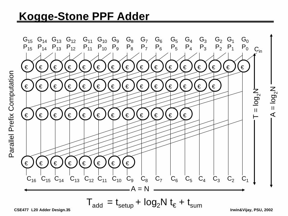
Kogge-Stone PPF AdderP
aral
lel P
refix
Com
puta
tion
€
G0P0
G1P1
G2P2
G3P3
G4P4
G5P5
G6P6
G7P7
G8P8
G9P9
G10P10
G11P11
G12P12
G13P13
G14P14
G15P15
€€€€€€€
€ € € €
€
€
€
€
C1C2C3C4C5C6C7C8C9C10C11C12C13C14C15C16
Cin
€
T =
log 2N
A =
log 2N
A = N
€€€€€€€
€ € € € € € € € € €
€ € € € € € € € € €
€ € € € € €
Tadd = tsetup + log2N t€ + tsum

CSE477 L20 Adder Design.36 Irwin&Vijay, PSU, 2002
More Adder Comparisons
0
10
20
30
40
50
60
70
8 bits 16 bits 32 bits 48 bits 64 bits
RCACSkAVSkAKS PPA
CSE477 L20 Adder Design.37 Irwin&Vijay, PSU, 2002
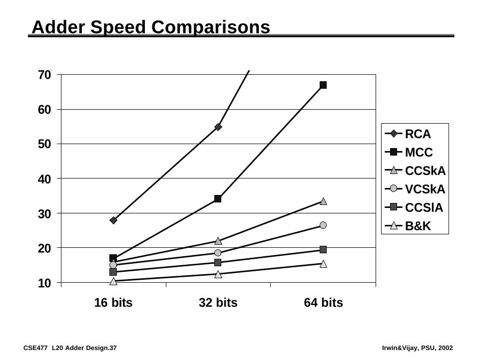
Adder Speed Comparisons
10
20
30
40
50
60
70
16 bits 32 bits 64 bits
RCAMCCCCSkAVCSkACCSlAB&K

CSE477 L20 Adder Design.38 Irwin&Vijay, PSU, 2002
Adder Average Power Comparisons
0
5
10
15
20
25
30
35
16 bits 32 bits 64 bits
RCAMCCCCSkAVCSkACCSlAB&K
CSE477 L20 Adder Design.39 Irwin&Vijay, PSU, 2002
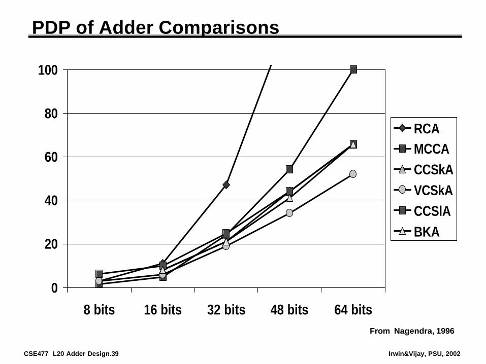
PDP of Adder Comparisons
0
20
40
60
80
100
8 bits 16 bits 32 bits 48 bits 64 bits
RCAMCCACCSkAVCSkACCSlABKA
From From NagendraNagendra, 1996, 1996

CSE477 L20 Adder Design.40 Irwin&Vijay, PSU, 2002
Next Lecture and Remindersq Next lecture
l Multiplier Design- Reading assignment – Rabaey, et al, 11.4
q Remindersl Project final reports due December 5th
l HW5 (last one!) due November 19th
l Final grading negotiations/correction (except for the final exam) must be concluded by December 10th
l Final exam scheduled- Monday, December 16th from 10:10 to noon in 118 and 121
Thomas