debugging serial bus systems with a mixed-signal...
TRANSCRIPT

Debugging Serial Bus Systems with a Mixed-Signal Oscilloscope
Application Note 1395
Who Should Read This Application Note?
This application note is for digital
designers in R&D working with both
analog and digital components,
including microcontroller and DSP
systems using serial buses. This
application note discusses the
challenges associated with and new
solutions for debugging serial bus
designs including a Controller Area
Network (CAN), Inter Integrated
Circuit (I2C), Serial Peripheral
Interface (SPI), or Universal Serial
Bus (USB).
Introduction to Serial Bus Protocols
For many years, parallel buses
have been the primary method for
communicating with peripheral
devices in microcontroller and
DSP-based designs. Microcon trollers
and DSPs are used in many types of
applications from consumer products,
such as a cell phone, to control of the
electrical system in a car, to many
different types of embedded systems
including industral applications.
In these types of applications, bus
speeds typically operate in the tens
of megahertz and below range.
Because these applications continue
to grow in complexity while trying to
maintain minimal costs, serial buses
are commonly used as the method
for communicating between devices
and peripherals. In addition to a lower
cost contribution, serial bus designs
use less power, and fewer pins and
therefore require less board space.
Serial buses allow for the
transmission of data over a serial
line with a minimal amount of
control lines and connections.
Today, there are a large number of
devices designed with serial protocol
interfaces by many manufacturers.
These buses are widely used for
interfacing microcontrollers and
DSPs to EEPROMs, analog to digital
converters, sensors, actuators,
and many other peripherals.
These systems are often used as
control buses and networks inside
TV equipment, cellular phones,
automobiles, and in many other
industrial applications.
The major advantage of using a
serial bus is the small number of
signals required. A disadvantage
of serial interfacing is the tradeoff
of speed for space in the design.
The microcontroller’s I/O port
can spend a significant amount of
time communicating with a serial
device. Another disadvantage of
using a serial bus in a mixed analog
and digital design is in debugging
problems in the system. The difficulty
lies in extracting information about
the protocol itself and in determining
the interactions between devices
from a long serial stream of data.
Table of Contents
Introduction to Serial Bus Protocols ................................................................... 1
Debugging Serial Bus Systems with a Mixed-Signal Oscilloscope (MSO) ... 2
Inter-Integrated Circuit (I2C) Introduction ........................................................... 4
Debugging an I2C Bus System with the MSO Trigger Features ..................... 5
Debugging an I2C Bus System with the MSO Hardware-accelerated
Decode Features ...................................................................................................... 8
Serial Peripheral Interface (SPI) Introduction .................................................... 9
Debugging an SPI Bus System with the MSO Triggering Features ............. 10
Controller Area Network (CAN) Introduction ................................................... 11
Debugging a CAN Bus System with the MSO Triggering Features ............. 13
Universal Serial Bus (USB) Introduction ........................................................... 15
Debugging a USB System with the MSO Triggering Features ..................... 16
Summary ................................................................................................................. 18
Warranty Information (Remove All Doubt) .........................................Back cover
Contact Agilent ........................................................................................Back cover

2
Debugging Serial Bus Systems with a Mixed-Signal Oscilloscope
There are different types of
measurement problems encountered
when debugging mixed analog and
digital serial bus designs. Designers
may need to debug the behavior of
the serial bus protocol itself or they
may be using an established serial
protocol connection to get an entire
design to communicate and work
together properly. In the former case,
the user would most likely use an
oscilloscope to debug the physical
layer of the protocol. Parametric
measurements such as rise and
fall time, setup and hold times, and
analyzing voltage levels could be
made on signals in the system, such
as the clock and data lines. For the
latter problem, the designer may want
to look at functional and integration
issues within the system, which may
require analyzing relative timing and
data content on the bus.
Debugging problems like these in
today’s serial bus designs can be
quite a challenge using traditional
methods. A common method for
debugging these systems has been
to use a logic analyzer combined
with an oscilloscope. However,
triggering on a serial bus transition
of interest can be difficult because
there is no time reference to all of
the data since it is read sequentially
bit-by-bit. In the past, debugging a
parallel bus with a logic analyzer was
fairly straightforward by setting up
a pattern or state trigger to find the
interaction of interest.
However, setting up a logic analyzer
to trigger on content within a long
serial data stream is another matter.
To trigger the logic analyzer on a
serial pattern within a protocol
requires the user to create a state
machine that looks for the desired
bit pattern or frame in the protocol.
Unfor tunately, most logic analyzer’s
state machines are usually only 16
levels deep, which does not meet the
necessary depth to look for a problem
in a long serial stream of data.
This solution also would require a
lengthy process of measurement
setups, which would probably
result in a significant amount of
user frustration. If the usered
needs to make parametric types
of measurements on the system,
correlating the logic analyzer with
an oscilloscope would be even
more time consuming. It would also
require deep memory records on both
instruments to view the long serial
streams of data. With demanding
schedules and project deadlines,
most designers would agree that
better techniques and tools are
necessary for debugging designs that
include serial bus technologies.
To meet and beat these challenges,
Agilent invented the mixed-signal
oscilloscope (MSO) in 1996 as an
effective method for debugging serial
bus interfaces with specially designed
triggering and decode capabilities for
serial protocols. These features solve
the difficult problem of triggering on
the specific protocol conditions with
a logic analyzer and oscilloscope.
The Agilent MSO automatically finds
the desired pattern in the long serial
stream without the chore of creating
a complicated state machine in a
logic analyzer. The MSO is a single
instrument with 16 digital timing
channels and two or four analog
scope channels with bandwidths
up to 1 GHz. In addition, the MSO
has very deep memory acquisition
records using Agilent MegaZoom III
technology. These triggering features
are easy to set up and can reduce the
time you currently spend in debugging
problems in embedded systems that
utilize serial bus communications.
The serial bus applications features
in the MSO can trigger and decode
serial buses with a synchronous
clock, such as the I2C and SPI
buses that have separate clock
and data lines. And those with an
asynchronous clock like RS232 and
other UART protocols. In addition, the
Agilent MSO is also able to establish
a trigger and decode serial buses that
have an embedded clock within the
data stream, such as CAN and USB.
These powerful triggering and decode
features make it easy to correlate the
sequential data and timing on long
streams of data.
With up to 8 Mbytes of MegaZoom
III deep memory, the Agilent MSO
can easily and quickly capture and
analyze long serial streams. With
one instrument, MegaZoom III deep
memory gives you the ability to
look at the fast digital signals and
correlate those with slow analog
signals on long serial data streams.
Also, the MSO’s sixteen digital
and two or four analog channels of
acquisition are automatically time
correlated. The dilemma of having
to trigger twice to get a long time
capture or to see detailed resolution
is solved with MegaZoom III deep
memory.

3
Debugging Serial Bus Systems with a Mixed-Signal Oscilloscope (continued)
Figure 1 shows an example of a
microcontroller-based design that is
used to control and monitor devices
around the home. The microcontroller
communicates with an RF transceiver,
an RS232 bridge, an EEPROM, a
keypad, and a display over the
SPI bus. The MSO is the perfect
debug tool for this design. With the
combination of analog and digital
channels, the user can correlate
activity on the serial bus with what
is taking place in other parts of the
system. This makes it easier to debug
the source of a serial bus problem,
such as a missing acknowledge,
handshake, or an unintended packet
loss. Additionally, the triggering and
decode features give the ability to
look at the problems in real time
instead of capturing the data and
then using post processing to view
the data record. This way the user
can be sure that the signals being
viewed are accurate representations
of the current timing relationships in
the system.
Many designs incorporate more
than one type of serial interface
for communication. For example,
a design may use an I2C bus to
communicate locally to an EEPROM
and then another device may use a
SPI bus to communicate with other
peripherals in the design. The entire
design may then connect to an
external network via USB or CAN.
Having one instrument to debug many
parts of a system can reduce debug
time, cost, and frustration.
Using an Agilent MSO with
MegaZoom III deep memory and
protocol-specific triggering and
decode solves the new challenge of
finding and viewing problems within
a long stream of serial data in today’s
embedded designs with serial buses.
This application note describes the
Agilent MSO serial protocol triggering
and decode features including
I2C, SPI, CAN and USB, and how
these features make debugging
microcontroller and DSP-based
designs easier and more efficient
than ever before.
RF M-BusRS232
RS485
Microcontroller
1 2 3
4 5 6
7 8 9
0 #0p Amp
Voltage
Supervisor
Voltage
Regulator
EEPROM
LCD Displaycontrol and surveillance
of all controllable systems
used in the household,
e.g.
Possible applications:
- heating system
- alarm system
- smoke detectors
- metering systems
(electricity and water
flow meters etc.)
Keypad
Figure 1. Example of a microcontroller-based design used to monitor and control devices in the home. The microcontroller
uses the SPI bus to communicate with an RF tranceiver, an RS232 bridge, an EEPRPOM, a keypad, and display.

4
Inter-Integrated Circuit (I2C) Introduction
Philips originally developed the I2C
(Inter-Integrated Circuit) bus for
communication between devices
inside of a TV set. Today, I2C is used
in a broad range of applications
for efficient inter-IC control and is
supported by most semiconductor
vendors. The I2C bus consists of a
simple bi-directional two-wire bus
with two signal lines, SCL (serial
clock) and SDA (serial data). All I2C
bus compatible devices have an
on-chip interface that allows them
to communicate directly with each
other. Most I2C devices operate at
speeds up to 400-Kbps, with some
going into the low megahertz range.
The protocol is well defined and
has a built in addressing scheme
so there is no need for chip select
or logic controls. This makes it an
inexpensive and simple solution to
link many devices of an embedded
design together. When it was first
introduced, the I2C bus protocol
used 7 bits for addressing. To
accommodate the higher demand
for more address space the bus now
allows for 10-bit addressing and
speeds up to 3.4 MHz yet remains
backward compatible. Because
of its low cost, it is widely used
in many products, including cell
phones, audio/video instruments,
medical equipment, and industrial
applications. In fact, there are
hundreds of I2C compatible devices
available today. Examples of simple
I2C compatible devices found
in embedded systems include
EEPROMs, thermal sensors, and real-
time clocks.
The I2C bus physically consists of
two active signals and a ground
connection. The signals SDA and
SCL are both bi-directional. Every
component connected to the bus
has its own unique address, whether
it is a CPU, an LCD driver, or an
EEPROM. Each of these chips can
act as a receiver and/or transmitter
depending on their function. In
addition, there may be one or more
bus masters. The device that initiates
data transfer on the bus is considered
the bus master and all the others are
bus slaves. Masters are generally
microcontrollers, microprocessors, or
DSPs. Figure 2 shows an example of
an embedded system with an I2C bus.
Figure 2. Example of an I2C bus system. The I2C bus consists of two active signals, SDA and SCL.
Every component on the bus has its own unique address.
MICRO
Controller
A
LCD
Driver
Static
RAM or
EEPROM
GATE
ARRAY ADC
MICRO
Controller
B
SDA
SCL

5
Debugging an I2C Bus System with the MSO Trigger Features
Using a conventional oscilloscope to
debug and correlate data and timing
in a long serial stream can be difficult
and time consuming. A typical
problem could be a microcontroller
requesting information from a device,
such as an LCD controller, and then
not receiving any information back
from the slave device. Debugging this
problem with a conventional scope
would require the user to digitize
a long data record using either an
edge or pattern trigger. The user
would then need to scroll through
the individual data frames one-by-one
to search for the particular problem.
Using this technique would be very
time consuming.
Using an MSO with I2C triggering
features and deep memory is a
perfect solution for debugging
problems with devices on an I2C bus.
The four analog channels along with
16 digital timing channels make it
possible to probe the two signals
of the bus along with other signals,
such as the data and address lines
of an EEPROM, to see where the
problems are really occurring in the
system. With these features it is easy
to trigger and set up the address
and data conditions to debug the
common I2C bus conditions, which
could include a problem in the system
behavior or on a specific I2C frame.
I2C Trigger Features
Setting up the I2C triggering features
is simple. All of these features are
accessed through the easy-to-use
interface of the MSO. After assigning
the data (SDA) and clock (SCL) to
Figure 3. Setting up I2C triggering on the mixed-signal oscilloscope.
The MSO quick help screen gives detailed instructions on how to use
the I2C triggering features.
specific scope channels, the user can
then select the I2C serial triggering
options, as shown in Figure 3. The
two lines of the bus can be probed by
either the digital timing channels or
the analog scope channels and are
automatically labeled on the screen.

6
Debugging an I2C Bus System with the MSO Trigger Features (continued)
Content Triggering: Read or Write Frame of a Specifi c Address and Data Value
In a typical I2C frame, there is a
start condition, a control byte that
configures the particular slave to
be read from or written to, a valid
acknowledge clock pulse, and then
other bytes of the transferred data.
The MSO can be easily configured to
trigger on the address and/or data
of the control byte or the secondary
byte.
This is a powerful triggering feature
that allows the user to look within
the I2C frame to trigger when a device
at a particular address is written to
or read from with a data value. For
example, in Figure 4 the MSO triggers
when a microcontroller writes the
data value 41 hex to a keypad at
address 50 hex on the I2C bus. This
feature can be very useful to find
errors in software routines that write
incorrect data to a device.
EEPROM Data Read Trigger
In the I2C protocol, EEPROMs have
a predetermined address on the bus
in the form of 1010xxx binary. The
EEPROM Data Read Trigger looks
for an address matching this pattern
on the SDA line, followed by a read
bit and then an acknowledge bit.
When the data matches the qualified
condition set by the user, the MSO
triggers on the acknowledge clock
edge after the data is sent.
The MSO can trigger on a “current
address read” cycle, a “random
read” cycle, or on any data byte
within a “sequential read” cycle. The
MSO trigger hardware looks for the
appropriate control byte first, followed
by any data byte that meets the
user-specified qualifications. These
qualifications include less than,
greater than equal, not equal, and
don’t care.
For example, suppose a
microcontroller stores calibration data
from a temperature sensor in memory
to use at a later time in a program.
But when the data is read back, it
is corrupt and causes the sensor
to perform incorrectly. This trigger
feature of the MSO would give the
user a quick and easy way to track
and debug data being read from an
EEPROM in the system.
Figure 4. I2C trigger on a Write Frame with Address and Data. This powerful triggering
feature allows the user to look within the 12C frame to trigger when a device at a
particular address is written to or read from with a data value.

7
Debugging an I2C Bus System with the MSO Trigger Features (continued)
I2C Bus Start and Stop Trigger
Using the I2C protocol, a start
condition must be issued before any
transaction on the bus occurs. The
start condition acts as a signal to all
connected devices that a message is
about to be transmitted on the bus.
As a result, all connected chips will
listen to the bus. After a message is
sent, a stop condition occurs. This
is the signal for all devices on the
bus that the bus is free again. The
chip accessed during the message
will then process the received
information.
It could be very difficult to find a start
or stop condition on the I2C bus using
edge triggering with a traditional
scope; there could be hundreds of
pulses to scroll through. Using the I2C
start condition triggering, as shown
in Figure 5, the MSO triggers when it
detects a start condition by looking
for a high to low transition of the SDA
(data) line while the SCL (clock) line
is high.
I2C Bus Re-Start Trigger
Within a single message there can be
multiple Start conditions in a frame.
The MSO with I2C triggering is able to
find a restart within a frame after the
start condition occurs.
I2C Bus Missing Acknowledge Trigger
After each byte transfer, an
acknowledge is sent. This occurs
when the SDA line is pulled high
and the SCL line is pulsed. If a
device never sends an acknowledge
command, it can cause the bus to
hang up and it could be difficult to
find the actual problem. Is it the
microcontroller not sending the
correct address information or is the
slave device not responding? Setting
up the MSO to trigger on a missing
acknowledge can help isolate a
problem such as this very quickly. It
will find a missing acknowledge event
anywhere in an address/control byte
or data byte of any size
12C frame.
10 Bit Write Trigger
Ten-bit addressing allows the use
of up to 1024 addresses to prevent
problems with the allocation of
slave addresses as the number of
I2C devices continues to expand. The
MSO triggers on a 10-bit write to an
address in a frame if all data in the
pattern matches.
The MSO trigger features, designed
specifically for the I2C protocol, make
debugging I2C buses easier than ever
before and allow the user to find
problems in real time whether they
are problems within the protocol
design itself or problems with devices
in a system.
Figure 5. Start of Frame trigger. The MSO triggers when it detects a start condition by
looking for a high to low transition of the SDA (data) line while the SCL (clock) line is
high.

8
Debugging an I2C Bus System with the MSO Hardware-accelerated Decode Features
Because the I2C serial protocol is
widely used today in mixed-signal
embedded designs for chip-to-chip
communication between EEPROMs,
DACs, ADCs, and other peripheral ICs
to microcontrollers, microprocessors
and DSPs, it transfers many bits of
data serially, it can be very difficult
to unravel what’s happening in an
embedded system with conventional
scope triggering. With the MSO’s
integrated analog and digital channel
triggering capabilities, we can
synchronize the oscilloscope’s display
on specific chirps and verify the
serial data transmissions by using
the hardware-accelerated decode
solution.
Hardware-accelerated Decode: Find and Debug Intermittent Serial Bus Errors and Signal Integrity Problems Faster
Other oscilloscope solutions with
serial bus triggering and protocol
decode typically use software post-
processing techniques to decode
serial packets/frames. Using these
software techniques, waveform- and
decode-update rates tend to be slow
(sometimes seconds per update),
especially when you use deep
memory, which is often required to
capture multiple packetized serial
signals.
Hardware-accelerated decode allows
for faster decode update rates, which
enhance the scope’s probability
of capturing infrequent serial
communication errors. The MSO
is a crucial debug tool for verifying
and debugging embedded designs
that include a combination of analog
signals, serial traffic, and higher-
speed digital control signals found
in today’s embedded designs. MSOs
provide an integrated way to capture,
decode and time-correlate multiple
analog, serial and digital signals of
various speeds as shown in Figure 6.
Color-coded, Hardware-accelerated Data Decode
Decoding I2C serial bus is simple with
just a click of a button to turn on
serial decode and a menu selection
for the type of serial mode being
used. With the color coded display of
the serial packets on screen, you can
easily correlate the packet decode
to the analog or digital signals the
MSO captured. The MSO also has
the ability to trigger on another signal
type in the embedded system while
decoding the I2C serial traffic. This
allows for a whole embedded system
debug solution approach to verifying
mixed-signal embedded designs.
Figure 6. On-screen serial decode of I2C data packet shown with
time-correlated analog and digital waveforms captured by an
MSO.

9
Serial Peripheral Interface (SPI) Introduction
The Serial Peripheral Interface,
SPI, is a serial bus standard
originally introduced by Motorola
with interfaces available on
many popular communication
processors and microcontrollers.
Like I2C, SPI provides good support
for communication with slow
peripheral devices that are accessed
intermittently, such as EEPROMs
and real-time clocks. However, SPI is
better suited than I2C for applications
that are thought of as data streams
because of its high bandwidth (in
the tens of megahertz), whereas I2C
devices read and write to addressed
locations in a slave device. An
example of a data stream application
is the data communication between
microprocessors, microcontrollers,
A/D converters, D/A converters, or
DSPs.
Devices on a SPI bus communicate
using a master/slave relationship,
in which the master, usually the
microcontroller, initiates the data
transfer. When the master generates
a clock and selects a slave device,
data can be transferred in either
or both directions at the same
time (called full-duplex mode).
The protocol helps the device to
determine if the data is a valid signal
or not, depending on bits set in the
frame.
The SPI bus consists of two data
lines and two control lines. The data
lines are MOSI (master data output/
slave data input) and MISO (master
data input/slave data output). The
control lines include SCLK (serial
clock), and SS (slave select). The
master may transmit data at a variety
of data rates. The serial clock control
line is driven by the master and
controls the flow of the data bits and
cycles once for each bit transmitted.
The slave select control line allows
slaves to be turned on and off with
hardware control. Unlike I2C, the SPI
protocol does not have a start of
frame; the chip select or slave select
(SS) going high or low (depending
on the device) frames the data.
Figure 7 shows a block diagram of a
web phone, which is an example of a
multi-slave system.
DAA1
DAA2
McBSP0
McBSP1
McBSP2
Dual
Channel
AIC
DSP
Data - SPI
Voice - SPI
Phone - SPI
FLASH DPRAM
EPLDEPLD
Loader
Power
Supply
Single
Channel
AIC
HS
DET
2/4
HYB
T1
T2
R1
R2
Figure 7. Web Phone Block Diagram; example of a multi-slave SPI bus, DSP-based system.

10
Debugging an SPI Bus System with the MSO Triggering Features
Because SPI does not have a formal
standard, there are many different
types of implementations. Common
debug problems in SPI systems
involve configuring the clock rate for
the controller as well as the phase
and polarity for how each peripheral
clocks data in and out. For example,
in the web phone device shown in
Figure 8, some devices may or may
not clock data in and out using the
same polarity and phase of the clock.
Because of this, there could be
difficulties configuring the devices on
the bus.
An MSO with SPI triggering features
and deep memory is a great tool
for debugging long serial streams,
where configuration errors may
cause problems in the system. In
the previous web phone design,
MegaZoom III deep memory allows
the user to correlate audio events,
in the 20 kHz range, with DSP digital
events, in the 10 MHz range, all in
the same acquisition. The user can
connect to the clock, data (either
MISO or MOSI) and chip select
framing (SS) signals in the target
system. As shown in Figure 8, the
two analog channels can monitor the
data and clock while the 16 digital
timing channels can monitor the chip
select lines attached to the peripheral
devices.
The MSO triggers on a serial data
pattern during a framing period. The
clock slope can be set to either a
falling or rising edge. The serial data
string can be specified to be from 4
to 32 bits long, and the individual bit
values in the frame can be assigned
to either a L, H, or X (don’t care)
condition. Making things even easier,
the CS, Clock and Data labels for the
source channels are automatically set
up on the screen.
The user must select a framing signal
for the MSO serial trigger hardware
to detect. This framing signal can
be a high chip select (SCS) or a low
chip select (˜CS). Also, the MSO
can generate its own framing signal
after a user- specified time of clock
inactivity. The MSO requires a setup
time of 50 ns from the framing signal
going true to the first active clock
edge. The data setup and hold times
are 10 ns and 5 ns, respectively. The
MSO will trigger on the Nth clock
edge (from 4 to 32) if the specified
data pattern is true.
This is a very elegant and easy-to-
use solution, especially compared
to previous methods using a logic
analyzer and an oscilloscope, which
don’t work well for debugging serial
bus systems. Using an MSO, the
user does not have to create a state
machine by hand to find the desired
pattern in a serial stream of data,
nor does the user have to correlate
measurements with an oscilloscope.
The MSO does the work to find the
pattern of interest, all in a few easy
steps. Debugging an SPI bus would
traditionally have been very difficult
to perform, but the Agilent MSO has
just the right features to save design
engineers time debugging problems in
order to spend more time designing.
Figure 8. Setting up and triggering on SPI signals. The MSO will trigger on the Nth clock
edge (from 4 to 32) if the specifi ed data pattern is true.

11
Controller Area Network (CAN) Introduction
The Controller Area Network (CAN) is
an ISO-defined serial communications
bus for real-time applications. It was
originally introduced by Bosch in
the 1980s to provide a cost-effective
communications bus for automotive
electronics. The CAN serial bus
operates at data rates of up to
1-Mb/s, has excellent error detection
capabilities, and is extremely reliable.
Because of these features, the CAN
serial communications bus continues
to be widely used throughout the
automotive industry and is gaining
acceptance in manufacturing,
aerospace, and in many other
industrial applications involving data
communication between systems and
sub-systems.
An example CAN bus system of an
automobile is shown in Figure 9. A
typical automobile system can have
several different CAN networks
operating at different speeds and
performing different tasks. For
example, there may be a high-speed
network for the power-train system
and separate networks for the climate
control, lights, and anti-lock brake
systems.
The CAN serial bus system has multi-
master capabilities, meaning that all
CAN nodes can transmit data, and
multiple CAN nodes can request data
from the bus at the same time.
Unlike a traditional network, CAN
does not send messages from one
point to another. In a CAN network,
there is no addressing of devices in
the usual sense because it is the
data, not the device, that is given an
identifier. A priority scheme called
Carrier Sense, Multiple Access with
Collision Detect (CSMA/CD) defines
which device is the controller of
the bus at a particular time. The
identifier with the lowest numerical
value has the highest priority and will
therefore gain control of the bus. Any
po tential bus conflicts are resolved
in hardware. A message is broadcast
to the network and any node that
has interest in the message can pick
up the data. Additionally, the CAN
bus is a two-wire bus with signals
called CAN_HI
and CAN_LOW
. With its
differential voltage design, the CAN
bus has good noise immunity and
fault tolerance characteristics.
Figure 9. Example CAN automobile system. (Diagram courtesy of Motorola Inc.)

12
Controller Area Network (CAN) Introduction (continued)
Low-cost CAN controllers,
microcontrollers with embedded CAN
controllers, and interface devices are
available as off-the-shelf parts from
many semiconductor manufacturers.
Figure 10 shows a typical CAN node
that includes a microcontroller with
a dedicated CAN controller using
an external address bus. Some
controllers are designed to interface
either as parallel devices on the
address bus or by using another serial
bus interface, such as SPI. The CAN
transceiver has both a transmit and
a receive side, so that it can write to
and read from the bus simultaneously.
An example of a CAN node is shown
in Figure 10. This could be a system
node for a power window, engine
monitoring, or suspension control in
an automobile.
Figure 10. Example CAN node.
System MCU
CANBus Line
_INT
_CS
ALE
_RD
_WR
_WAIT
AD7-0
RESET
PORT
SD0
SDI
SCLK
A7-0
_INT
_CS
PALE
_PRD/SRW
_PWR
_PRDY/SWAIT
AD7-0
_RESET
Rx0
Rx1
Tx0
Tx1
RxD
Vref
TxD
RS
CAN H
CAN L
Vcc GND
10 kΩ
10 kΩ
+5V

13
Debugging a CAN Bus System with the MSO Triggering Features
There are four different types of
communication on the CAN bus.
A message frame contains the
application data, a remote frame
requests data from the network,
an error frame reports errors to
each node, and an overload frame
delays transmission of a CAN
frame if the receiver circuitry of a
node is not ready. The MSO CAN
triggering modes provide the ability
to synchronize to any message frame,
remote transfer request frame, or
overload frame.
Since a frame of information is
usually a known place in the
operation of a CAN node, this allows
for a synchronous look at other
signals on that particular CAN node.
Shown in Figure 11 is the MSO Quick
Help description of the CAN standard
frame format. At the beginning of
the frame is the Start Of Frame (SOF)
bit. The MSO triggering capabilities
allow the user to synchronize the
scope acquisition to the start of a
CAN frame, permitting oscilloscope
user to look at other operations and
signals in their design that are time-
correlated to the CAN bus traffic.
These triggering features operate on
either the CAN 2.0B format with a
29-bit identifier or 2.0A with an 11-bit
identifier.
One example of how these features
can be useful is to debug automotive
applications in real time. For instance,
a message that causes the engine
to start could also cause noise from
the engine to be induced into the
electronic control system. This noise
would be synchronous to the Start
of Frame and could be difficult to
isolate. Using edge triggering to find
a problem like this would require the
user to scroll through many pulses in
a waveform and could be very difficult
to synchronize and correlate to the
data. But with the SOF triggering
capability, this activity is synchronous
to the trigger of the MSO. The user
can probe using the analog channels
to see the noisy components of the
signal. With MegaZoom III deep
memory, the user can then look
back in time in the frame so that the
problem can easily be isolated and
analyzed to find the cause of the
noise problem.
Figure 11. CAN trigger Quick Help description. The MSO
triggering capabilities allow the user to synchronize the
scope acquisition to the start of a CAN frame.

14
Debugging a CAN Bus System with the MSO Triggering Features (continued)
CAN Trigger Features
With an MSO, the user can probe
a CAN signal with any of the four
analog or 16 digital timing channels
or a combination of analog and digital
channels. When using only one of
the channels to synchronize to the
CAN frame, 17 other channels remain
to provide a broader view into the
design. These 17 channels, coupled
with Agilent Technologies MegaZoom
III deep memory, give an unparalleled
breadth and depth of insight into
complex embedded CAN node
designs and interactions.
Specify Baud Rate
To synchronize to the bus traffic
correctly, the user can specify the
Baud Rate of the system. The baud
rates allowed follow the CiA (CAN
in Automation) trade associations
recommended baud rates.
Trigger Signals Include CAN_H,
CAN_L, Rx, or Tx
The user can also specify the
CAN-based signal to monitor. It can
be either of the differential CAN
signals, CAN_H or CAN_L. These are
useful for monitoring the bus itself,
especially when they are the only
signals the user has access to. Using
an MSO, it can also be useful to
look at parametric information about
these signals, including noise spikes,
ringing, and timing measurements.
Because these are differential signals
designed for a noisy environment,
noise spikes may cause false triggers
to occur while looking at a CAN_H or
CAN_L signal. To counter this, use a
differential probe such as the Agilent
N2772A 20 MHz differential probe,
to look at the actual noise-immune
differential signal. A signal type
selection, titled ‘Differential’ in the
menu system, is available for this
case.
The user can also probe the Rx and
Tx on the digital side transceiver
signals. The Rx signal gives a view
of all of the traffic on the bus and is
included for ease of access. The Rx
signal should not be susceptible to
noise/level drift on the physical bus
line CAN_H and CAN_L. The Tx line
provides more information because
it has activity on it only when the
source node is sending a message
on the bus. Probing this line can help
isolate the traffic to a particular node.
Real-time triggering combined with
MegaZoom III deep memory, four
analog and 16 timing channels
makes the MSO a great tool for
debugging CAN systems. The MSO’s
CAN protocol trigger features help
the user to easily synchronize
to the data frames of interest,
making it easier to find problems in
automotive and industrial designs.
For communications within an
automotive electronic module, an SPI
interface is commonly used. Because
the MSO has the ability to trigger on
multiple types of serial buses, it is an
invaluable measurement instrument
for debugging CAN system in not only
automotive applications but also in
many industrial control systems.
Figure 12. The user can specify the CAB-based signal to monitor. Shown here is a CAN-L
signal.

15
Universal Serial Bus (USB) Introduction
The Universal Serial Bus (USB)
provides a high data rate and an
easy connection from a PC to a wide
variety of multimedia and networked
USB peripheral devices. The USB
port of a PC enables a user to add
peripherals to the system without
having to open the system chassis.
Additionally, USB allows users to run
numerous devices, such as printers,
scanners, digital cameras, and
speakers, from a single PC.
Peripherals such as hubs and hosts
operate at full speed (12-Mb/s) or
low speed (1.5-Mb/s). These speeds
are adequate for devices such as
mice or keyboards, but would be
very limiting and not usable for next-
generation imaging and video devices,
such as high-resolution printers
and scanners, video-conferencing
cameras, and read/write (R/W) DVD
drives. For these types of devices,
high-speed USB increases data
throughput by a factor of 40 over full
speed USB to 480-Mb/s. The USB
2.0 version incorporates low, full,
and high speeds and is a backward
compatible extension of USB 1.1
using the same cables, connectors,
and software interfaces.
USB also supports plug-and-play
capability for automatic device
detection and installation. USB has
become a standard in the PC industry;
virtually every new PC today has
one or more USB ports. Figure 13
shows a typical USB system with a
PC connected to many peripherals
through a hub.
USB High-SpeedHub
USB Full-SpeedHub
USB 2.0 Peripheral
480 Mb/s
480
Mb/
s
12 Mb/s
12 M
b/s
12 Mb/s
12 M
b/s
Figure 13. Example USB system.
16
Debugging a USB System with the MSO Triggering Features
Debugging the physical layer of a USB
device is dependent on the visibility
into the system. For instance, a USB
keyboard controller might consist of
a microcontroller, an EEPROM, and
other devices encapsulated into a
single package. In this case, the user
only has access to the USB interface
line to the keyboard and cannot probe
the internal devices in the controller
unit. If pressing the CAPS LOCK key
does not turn on the LED on the
keyboard, there could be a number
of potential sources of the problem.
These include but are not limited to a
problem in a software setup, a device
failure, or a protocol error. To view
dependencies and setup conditions
it is important for the test equipment
to isolate the USB packets in order
to find where problems in the system
may be occurring.
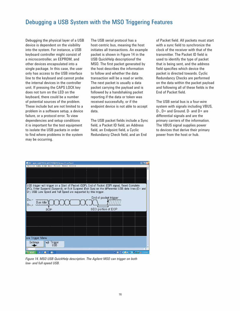
The USB serial protocol has a
host-centric bus, meaning the host
initiates all transactions. An example
packet is shown in Figure 14 in the
USB QuickHelp descriptionof the
MSO. The first packet generated by
the host describes the information
to follow and whether the data
transaction will be a read or write.
The next packet is usually a data
packet carrying the payload and is
followed by a handshaking packet
reporting if the data or token was
received successfully, or if the
endpoint device is not able to accept
data.
The USB packet fields include a Sync
field, a Packet ID field, an Address
field, an Endpoint field, a Cyclic
Redundancy Check field, and an End
of Packet field. All packets must start
with a sync field to synchronize the
clock of the receiver with that of the
transmitter. The Packet ID field is
used to identify the type of packet
that is being sent, and the address
field specifies which device the
packet is directed towards. Cyclic
Redundancy Checks are performed
on the data within the packet payload
and following all of these fields is the
End of Packet field.
The USB serial bus is a four-wire
system with signals including VBUS,
D-, D+ and Ground. D- and D+ are
differential signals and are the
primary carriers of the information.
The VBUS signal supplies power
to devices that derive their primary
power from the host or hub.
Figure 14. MSO USB QuickHelp description. The Agilent MSO can trigger on both
low- and full-speed USB.

17
Debugging a USB System with the MSO Triggering Features (continued)
USB Trigger Features
In the USB trigger mode, the Agilent
MSO can trigger on both low- and
full-speed USB. The user can probe
the differential lines, D+ and D-,
with any of the 2 analog lines or 16
digital timing lines using the following
trigger modes:
Start of Packet (SOP),
End of Packet (EOP)
The SOF packet consists of an
11-bit frame number. The Agilent
MSO triggers at the Sync bit at the
beginning of the packet.
The End of Packet is a field within
a USB packet and is signaled by
a Single Ended Zero (SE0) for a
specified number of bit times. The
Agilent MSO triggers at the end of
the SE0 portion of the End of Packet.
Enter Suspend, Exit Suspend
A USB device will enter suspend
when there is no activity on the
bus for greater than 3.0-ms. The
MSO triggers when the bus is idle
for greater than 3-ms. In the Exit
Suspend trigger mode, the MSO
triggers when exiting an idle state for
greater than 10 ms in order to see the
suspend/resume transition.
Reset Complete (RC)
In the Reset Complete trigger mode
the MSO will trigger when a Single
Ended Zero (SE0) is greater than
10 ms.
There are many instances where
the USB trigger modes are useful
for debugging the physical layer
of the USB protocol. With these
trigger modes, the user is able to
synchronize to USB packets being
communicated over a USB connection
between a host and a USB peripheral
device, making it easier to correlate
relationships within the protocol to
find problems in the system.
Figure 15. The Agilent MSO triggers at the sync bit at the beginning of the packet.
18
Summary
New technology trends bring
with them new design and debug
challenges. Agilent’s mixed-signal
oscilloscope (MSO) provides an
added dimension to solving problems
when debugging microcontroller and
DSP-based designs incorporating
serial buses. Agilent has solved the
problems associated with debugging
serial bus interfaces by providing
a unique solution that uses a MSO
with specially designed triggering
and decode capabilities to easily
debug protocols and the interactions
of devices on these buses. Having
one easy-to-use instrument to debug
many parts of a system can reduce
debug time, cost, and frustration
helping to get designs out the door
and into production faster. The
advantages of using an MSO include:
The powerful serial triggering
features allow for real time
triggering to correlate timing
relationships in microntroller
and/or DSP-based designs using
I2C, SPI, CAN, LIN, RS-232/UART
or USB serial protocols.
Serial protocol trigger features are
easy to use and set up; there is
no need to design a complicated
state machine in a logic analyzer to
debug serial protocols.
Agilent’s MSO has four analog
channels and 16 digital channels
to make parametric, timing, and
functional measurements all in one
instrument.
With up to 8 Megabytes of
MegaZoom III deep memory,
the MSO can easily and quickly
capture and analyze long serial
streams and correlate fast digital
signals with slow analog signals,
all in one acquisition.
•
•
•
•
Industry’s fastest waveform update
rate at 100,000 waveforms/sec
update rate max (with analog, digital,
and serial) combined with a fast,
high-definition 12.1” display with 256
levels of intensity, the Agilent MSO
reveals subtle waveform details that
most other oscilloscopes miss.
QuickHelp instructions (in 11
languages) give details on how to
use these powerful capabilities.
The unique 2+16- and 4+16-channel
mixed-signal oscilloscope (MSO)
models and the traditional 2- and
4-channel oscilloscope models
are optimized with just the right
capabilities to verify and debug
microcontroller and DSP-based
designs incorporating serial buses.
This combination of capabilities is
tailored to give the measurement
power needed to deliver higher
quality products to market faster.
•
•

19
Agilent Technologies Oscilloscopes
Multiple form factors from 20 MHz to > 90 GHz | Industry leading specs | Powerful applications

Remove all doubt
Our repair and calibration services
will get your equipment back to you,
performing like new, when prom-
ised. You will get full value out of
your Agilent equipment through-
out its lifetime. Your equipment
will be serviced by Agilent-trained
technicians using the latest factory
calibration procedures, automated
repair diagnostics and genuine parts.
You will always have the utmost
confi dence in your measurements.
For information regarding self
maintenance of this product, please
contact your Agilent offi ce.
Agilent offers a wide range of ad-
ditional expert test and measure-
ment services for your equipment,
including initial start-up assistance,
onsite education and training, as
well as design, system integration,
and project management.
For more information on repair and
calibration services, go to:
www.agilent.com/fi nd/removealldoubt
Agilent Email Updates
www.agilent.com/fi nd/emailupdates
Get the latest information on the
products and applications you select.
Agilent Direct
www.agilent.com/fi nd/agilentdirect
Quickly choose and use your test
equipment solutions with confi dence.
AgilentOpen
www.agilent.com/fi nd/open
Agilent Open simplifi es the process
of connecting and programming
test systems to help engineers
design, validate and manufacture
electronic products. Agilent offers
open connectivity for a broad range
of system-ready instruments, open
industry software, PC-standard I/O
and global support, which are
combined to more easily integrate
test system development.
www.lxistandard.org
LXI is the LAN-based successor to
GPIB, providing faster, more effi cient
connectivity. Agilent is a founding
member of the LXI consortium.
For more information on Agilent Technologies’ products, applications or services, please contact your local Agilent
offi ce. The complete list is available at:
www.agilent.com/fi nd/contactus
AmericasCanada (877) 894-4414 Latin America 305 269 7500United States (800) 829-4444
Asia Pacifi cAustralia 1 800 629 485China 800 810 0189Hong Kong 800 938 693India 1 800 112 929Japan 0120 (421) 345Korea 080 769 0800Malaysia 1 800 888 848Singapore 1 800 375 8100Taiwan 0800 047 866Thailand 1 800 226 008
Europe & Middle EastAustria 01 36027 71571Belgium 32 (0) 2 404 93 40 Denmark 45 70 13 15 15Finland 358 (0) 10 855 2100France 0825 010 700* *0.125 €/minute
Germany 07031 464 6333 Ireland 1890 924 204Israel 972-3-9288-504/544Italy 39 02 92 60 8484Netherlands 31 (0) 20 547 2111Spain 34 (91) 631 3300Sweden 0200-88 22 55Switzerland 0800 80 53 53United Kingdom 44 (0) 118 9276201Other European Countries: www.agilent.com/fi nd/contactusRevised: October 6, 2008
© Agilent Technologies, Inc. 2007, 2009Printed in USA, March 13, 20095988-5997EN
Product specifi cations and descriptions in this document subject to change without notice.
www.agilent.com