delft university of technology reducing switching
TRANSCRIPT

Delft University of Technology
Reducing Switching Artifacts in Chopper Amplifiers
Kusuda, Yoshinori
DOI10.4233/uuid:62585ae8-da35-459e-bf90-f53f7d0de32cPublication date2018Document VersionFinal published version
Citation (APA)Kusuda, Y. (2018). Reducing Switching Artifacts in Chopper Amplifiers.https://doi.org/10.4233/uuid:62585ae8-da35-459e-bf90-f53f7d0de32c
Important noteTo cite this publication, please use the final published version (if applicable).Please check the document version above.
CopyrightOther than for strictly personal use, it is not permitted to download, forward or distribute the text or part of it, without the consentof the author(s) and/or copyright holder(s), unless the work is under an open content license such as Creative Commons.
Takedown policyPlease contact us and provide details if you believe this document breaches copyrights.We will remove access to the work immediately and investigate your claim.
This work is downloaded from Delft University of Technology.For technical reasons the number of authors shown on this cover page is limited to a maximum of 10.
YoshinoriKusuda
ReducingSwitchingArtifacts
inChopperAmplifiers

Reducing Switching Artifacts in Chopper Amplifiers
Proefschrift
ter verkrijging van de graad van doctor aan de Technische Universiteit Delft,
op gezag van de Rector Magnificus prof. dr.ir. T.H.J.J. van der Hagen; voorzitter van het College voor Promoties,
in het openbaar te verdedigen op maandag 30 april 2018 om 15:00 uur
door
Yoshinori KUSUDA Elektrotechnisch ingenieur,
Master of Science van Tokyo Instituut van Technologie, Japan geboren te Kobe, Japan
Dit proefschrift is goedgekeurd door de promotor: Prof. dr. ir. K.A.A. Makinwa
Samenstelling promotiecommissie: Rector Magnicus, voorzitter Prof. dr. ir. K.A.A. Makinwa, Technische Universiteit Delft, promotor Onafhankelijke leden: Dr. Q. Fan Technische Universiteit Delft Prof. dr. ir. E. Cantatore Technische Universiteit Eindhoven Prof. dr. W.M.C. Sansen em.hgl Katholieke Universiteit Leuven Prof. dr. ir. A.J.P. Theuwissen Technische Universiteit Delft Prof. dr. ir. W.A. Serdijn Technische Universiteit Delft Prof. dr. ir. J.H. Huijsing em.hgl Technische Universiteit Delft
Printed by Ipskamp Printing, Enschede, the Netherlands
ISBN: 978-94-028-0997-8
Copyright © 2018 by Yoshinori Kusuda
All rights reserved. No part of this publication may be reproduced or distributed in any form of by any means, or stored in a database or retrieval system, without any prior permission of the copyright owner.

To my wife Kyoko and children Ryoko, Yukinori, and Kazunori

Contents
Chapter 1 Introduction.......................................................................................................... 1
1.1 Precision Data Acquisition Signal Chain ......................................................................... 2
1.2 CMOS Operational Amplifiers ........................................................................................ 3
1.2.1 Functionality ............................................................................................................. 3
1.2.2 Offset and Noise ....................................................................................................... 5
1.2.3 Summary ................................................................................................................... 6
1.3 Chopping Principle ........................................................................................................... 7
1.4 Traditional Applications of Chopper Op-Amps ............................................................... 8
1.4.1 Sensor Signal Conditioning ...................................................................................... 8
1.4.2 Current Sensing ....................................................................................................... 10
1.4.3 Summary ................................................................................................................. 11
1.5 Newer Applications of Chopper Op-Amps .................................................................... 12
1.5.1 Biomedical Sensing Front-End ............................................................................... 12
1.5.2 Reference and DAC Buffers ................................................................................... 13
1.5.3 Process Control Data Acquisition Signal Chain ..................................................... 14
1.6 Challenges ...................................................................................................................... 15
1.7 Organization of the Thesis ............................................................................................. 15
1.8 References ...................................................................................................................... 17
Chapter 2 Offset Cancellation Techniques ........................................................................ 21
2.1 Offset Trimming ............................................................................................................. 22
2.2 MOS Switches ................................................................................................................ 23
2.2.1 Realization and On-Resistance ............................................................................... 23
2.2.2 Charge Injection ...................................................................................................... 24
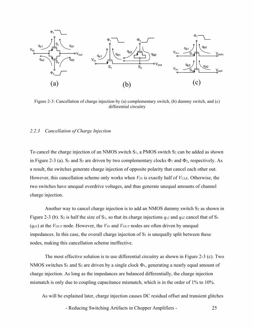
2.2.3 Cancellation of Charge Injection ............................................................................ 25
2.3 Auto-Zeroing .................................................................................................................. 27
2.3.1 Principle .................................................................................................................. 27
2.3.2 Residual Offset........................................................................................................ 27
2.3.3 Broadband Noise Folding ....................................................................................... 28
2.3.4 Ping-Pong Auto-Zeroing ......................................................................................... 30
2.4 Chopping ........................................................................................................................ 31

2.4.1 Up-Modulated Ripple ............................................................................................. 31
2.4.2 Glitches ................................................................................................................... 33
2.4.3 Input Bias Current and Residual Offset .................................................................. 34
2.4.4 Dynamic Switching Conductance ........................................................................... 38
2.4.5 Summary of the Errors ............................................................................................ 39
2.5 Comparison of the Techniques ....................................................................................... 42
2.6 References ...................................................................................................................... 43
Chapter 3 Methods of Reducing Chopper Switching Artifacts ....................................... 47
3.1 Residual Offset Reduction Techniques .......................................................................... 48
3.1.1 Filtering the Glitches ............................................................................................... 48
3.1.2 Dead-Timed Down-Modulation .............................................................................. 50
3.1.3 Nested Chopping ..................................................................................................... 50
3.2 Ripple Reduction Techniques ........................................................................................ 52
3.2.1 Multi-Path Chopper Offset Stabilization ................................................................ 52
3.2.2 Switched Capacitor Notch Filter ............................................................................. 54
3.2.3 High-Pass Filtering ................................................................................................. 56
3.2.4 Initial Offset Trimming ........................................................................................... 58
3.2.5 Combination with Auto-Zeroing ............................................................................. 58
3.2.6 AC-Coupled Ripple Reduction Loop ...................................................................... 62
3.2.7 Digitally Assisted Ripple Reduction Loop ............................................................. 64
3.3 Comparison of the Techniques ....................................................................................... 66
3.4 References ...................................................................................................................... 69
Chapter 4 Chopper Op-Amp with Auto-Correction Feedback ....................................... 71
4.1 Motivation ...................................................................................................................... 72
4.2 Op-Amp and Ripple Reduction Architecture ................................................................. 73
4.2.1 Basic Three Stage Chopper Op-Amp ..................................................................... 73
4.2.2 Auto-Correction Feedback ...................................................................................... 74
4.2.3 Switched Capacitor Notch Filter (SC-NF) .............................................................. 75
4.2.4 High Frequency Path (HFP) and Overall Op-Amp ................................................. 77
4.3 Residual Error Analysis ................................................................................................. 79
4.3.1 ACFB Loop Gain .................................................................................................... 80
4.3.2 Residual Ripple ....................................................................................................... 82
4.3.3 Residual Offset........................................................................................................ 82
4.3.4 Summary ................................................................................................................. 83
4.4 Circuit Implementation .................................................................................................. 86
4.4.1 Input and Nulling Transconductors ........................................................................ 86
4.4.2 Second, Output, and Feedforward Transconductors ............................................... 87
4.4.3 Clock Generator ...................................................................................................... 88
4.4.4 Noise Analysis ........................................................................................................ 91
4.5 Measurement Results ..................................................................................................... 92
4.6 Conclusions .................................................................................................................... 98
4.7 References .................................................................................................................... 100
Chapter 5 Chopper Op-Amp with Adaptive Clock Boosting Technique ..................... 103
5.1 Motivation .................................................................................................................... 104
5.2 Op-Amp Architecture ................................................................................................... 105
5.2.1 Conventional Three Stage Chopper Op-Amp and Frequency Compensation ...... 105
5.2.2 Frequency Compensation Using a Current Attenuator and a Dummy Differential
_______Output ................................................................................................................... 107
5.2.3 Overall Op-Amp Employing Auto-Correction Feedback ..................................... 109
5.2.4 ACFB Loop Gain Including Active Integrator ..................................................... 110
5.2.5 High Frequency Path (HFP) .................................................................................. 112
5.3 Transconductor Circuits ............................................................................................... 113
5.3.1 Input and Nulling Transconductors with the Current Attenuator ......................... 113
5.3.2 Noise Analysis and Optimization ......................................................................... 114
5.3.3 Residual Offset and CMRR Analysis ................................................................... 116
5.3.4 Second and Output Transconductors .................................................................... 117
5.4 Input Chopper ............................................................................................................... 118
5.4.1 Conventional CMOS Switches ............................................................................. 118
5.4.2 Input Chopper Employing Adaptive Clock Boosting Technique ......................... 119
5.4.3 Adaptive Clock Booster Circuit ............................................................................ 121
5.4.4 Common-Mode Buffer.......................................................................................... 123
5.5 Measurement Results ................................................................................................... 124
5.6 Conclusion .................................................................................................................... 130
5.7 References .................................................................................................................... 132
Chapter 6 Auto-Zero and Chopper Op-Amp with Clock Interleaving and Input Bias
_____________Current Trimming Techniques .................................................................... 135
6.1 Motivation .................................................................................................................... 136
6.2 Input Transconductor Architecture .............................................................................. 137
6.2.1 Previous High Voltage Input Transconductors ..................................................... 138
6.2.2 Capacitively-Coupled Auto-Zero and Chopper Input Transconductor ................ 139
6.2.3 Six Input Channels and Clock Interleaving .......................................................... 140
6.3 Input Bias Current Trimming ....................................................................................... 145
6.3.1 Input Switching Circuit Employing a Charge Mismatch Compensation Circuit . 146
6.3.2 Common-Mode Tracking Regulator ..................................................................... 147
6.4 Overall Op-Amp Implementation ................................................................................ 149
6.4.1 Overall Op-Amp Architecture .............................................................................. 149
6.4.2 One Channel Input Transconductor ...................................................................... 151
6.4.3 Second and Output Transconductors .................................................................... 153
6.4.4 Clock Generator and Level Shifter ....................................................................... 155
6.5 Measurement Results ................................................................................................... 156
6.6 Conclusion .................................................................................................................... 163
6.7 References .................................................................................................................... 164
Chapter 7 Conclusion ........................................................................................................ 167
7.1 Evolution over the Three Projects ................................................................................ 168
7.2 Benchmark ................................................................................................................... 174
7.3 Future Work ................................................................................................................. 176
7.4 Original Contributions.................................................................................................. 178
7.5 References .................................................................................................................... 179
Summary .................................................................................................................................... 181
Samenvatting ............................................................................................................................. 187
List of publications .................................................................................................................... 193
About the author ....................................................................................................................... 195
Acknowledgements ................................................................................................................... 197

- Reducing Switching Artifacts in Chopper Amplifiers - 1
Chapter 1
Introduction
This thesis describes the theory, design, and implementation of chopper amplifiers in CMOS
integrated circuits (ICs). As the name implies, such amplifiers employ chopping to achieve low
offset and low 1/f noise. Chopping is a circuit technique that involves up-modulating amplifier
offset and low frequency noise to higher frequencies, and which therefore can achieve microvolt-
level offset with very low temperature drift. On the other hand, it causes switching artifacts such
as AC ripple and glitches at the amplifier’s output, which usually need to be attenuated by low-
pass filtering, thus decreasing the usable signal bandwidth. As a result, the use of chopper
amplifiers has mainly been limited to low frequency applications. This thesis explores advanced
circuit techniques to reduce such switching artifacts without decreasing the usable signal
bandwidth, thus enabling the use of chopper amplifiers in a broader range of applications.
This chapter introduces the main objectives of this work. After a review of the key
requirements of amplifiers in signal chains, the offset and low frequency noise behavior of a
basic CMOS amplifier are described. Next, the chopping technique is presented, followed by a
description of its traditional use in low frequency applications. Some newer applications are then
described, which also require low offset and 1/f noise, but in which signal frequencies are too
high for switching artifacts to be reduced by low-pass filtering. Lastly, the challenges associated
with reducing switching artifacts in such applications are discussed.
- Reducing Switching Artifacts in Chopper Amplifiers - 2
1.1 Precision Data Acquisition Signal Chain
In today’s digital signal processing era, analog signals from the real world are ubiquitously
acquired and converted into digital signals for use in factories, test equipment, and healthcare
systems. The new Internet of Things (IoT) era will lead to the acquisition of even more analog
signals in vehicles, buildings, and even homes [1,2]. As a result, manufacturers will need to
develop a wide variety of data acquisition signal chains in less time and at lower cost. Those with
a resolution of 16 bits or higher are classified as precision data acquisition signal chains typically
intended for physical signals, such as light, sound, temperature, pressure, magnetic field, and
force. Such signals have relatively low frequency spectra ranging from DC to a few kilohertz or
at most up to a few hundred kilohertz.
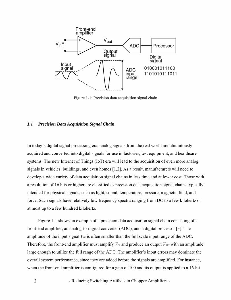
Figure 1-1 shows an example of a precision data acquisition signal chain consisting of a
front-end amplifier, an analog-to-digital converter (ADC), and a digital processor [3]. The
amplitude of the input signal Vin is often smaller than the full scale input range of the ADC.
Therefore, the front-end amplifier must amplify Vin and produce an output Vout with an amplitude
large enough to utilize the full range of the ADC. The amplifier’s input errors may dominate the
overall system performance, since they are added before the signals are amplified. For instance,
when the front-end amplifier is configured for a gain of 100 and its output is applied to a 16-bit
Figure 1-1: Precision data acquisition signal chain
- Reducing Switching Artifacts in Chopper Amplifiers - 3
ADC with a 5V full scale input, an input error of only 0.76V corresponds to one LSB error in
the resulting digital output. The offset and noise of the front-end amplifier must therefore be
lower than this in order to maintain true 16-bit performance.
Other common requirements of a front-end amplifier are a wide input range and high
common-mode rejection ratio (CMRR). This is because in certain applications, the input signals
may be associated with common-mode noise and disturbances. Some applications, e.g. bridge
readout, require the amplification of millivolt-level differential signals, while rejecting a few
volts of common-mode noise. Additionally, the amplifier’s input bias current should be low
enough for applications where the input signal sources have high impedances. On top of all these
requirements, cost and power efficiency are also important nowadays, especially since ADCs and
digital processors have become cheaper and more power efficient thanks to the steady scaling of
CMOS technology. In summary, front-end amplifiers are key elements of precision data
acquisition signal chains, and can dominate their overall performance and cost.
1.2 CMOS Operational Amplifiers
1.2.1 Functionality
A front-end amplifier can be integrated on a single chip with an ADC, or can be realized off-chip
with the help of a monolithic instrumentation amplifier (IA) or an operational amplifier (op-
amp). While the first two options often result in a more compact subsystem and/or optimized
performance, monolithic op-amp based implementations offer design flexibility. By modifying
their feedback networks, such op-amps can realize different closed-loop transfer functions and
accept various types of input signals, such as single-ended or differential, voltages or currents
etc. [4]. This thesis presents original op-amp designs implemented as monolithic ICs. However,
most of the theory and techniques presented are also applicable to IAs and other integrated
amplifiers.
- Reducing Switching Artifacts in Chopper Amplifiers - 4
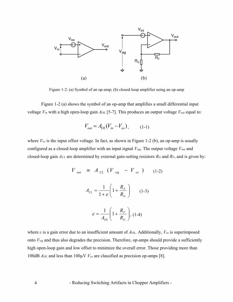
Figure 1-2 (a) shows the symbol of an op-amp that amplifies a small differential input
voltage Vin with a high open-loop gain AOL [5-7]. This produces an output voltage Vout equal to:
)( osinOLout VVAV , (1-1)
where Vos is the input offset voltage. In fact, as shown in Figure 1-2 (b), an op-amp is usually
configured as a closed-loop amplifier with an input signal Vsig. The output voltage Vout and
closed-loop gain ACL are determined by external gain-setting resistors RG and RF, and is given by:
)( ossigCLout VVAV (1-2)
G
FCL R
RA 1
1
1
(1-3)
G
F
OL R
R
A1
1 , (1-4)
where ε is a gain error due to an insufficient amount of AOL. Additionally, Vos is superimposed
onto Vsig and thus also degrades the precision. Therefore, op-amps should provide a sufficiently
high open-loop gain and low offset to minimize the overall error. Those providing more than
100dB AOL and less than 100µV Vos are classified as precision op-amps [8].
Figure 1-2: (a) Symbol of an op-amp; (b) closed-loop amplifier using an op-amp
- Reducing Switching Artifacts in Chopper Amplifiers - 5
1.2.2 Offset and Noise
Offset is a deterministic DC error and is usually the result of the systematic and random device
mismatch that occurs during IC fabrication. The amount of device mismatch depends on device
size and process technology. Since individual op-amps will then have unique offsets, only the
standard deviation and maximum value of this offset can be specified for a given design. Typical
CMOS op-amps have maximum offsets in the order of a few millivolts to tens of millivolts [9].
Offset can change with temperature and the input common-mode voltage; these changes are
expressed by offset drift and CMRR specifications.
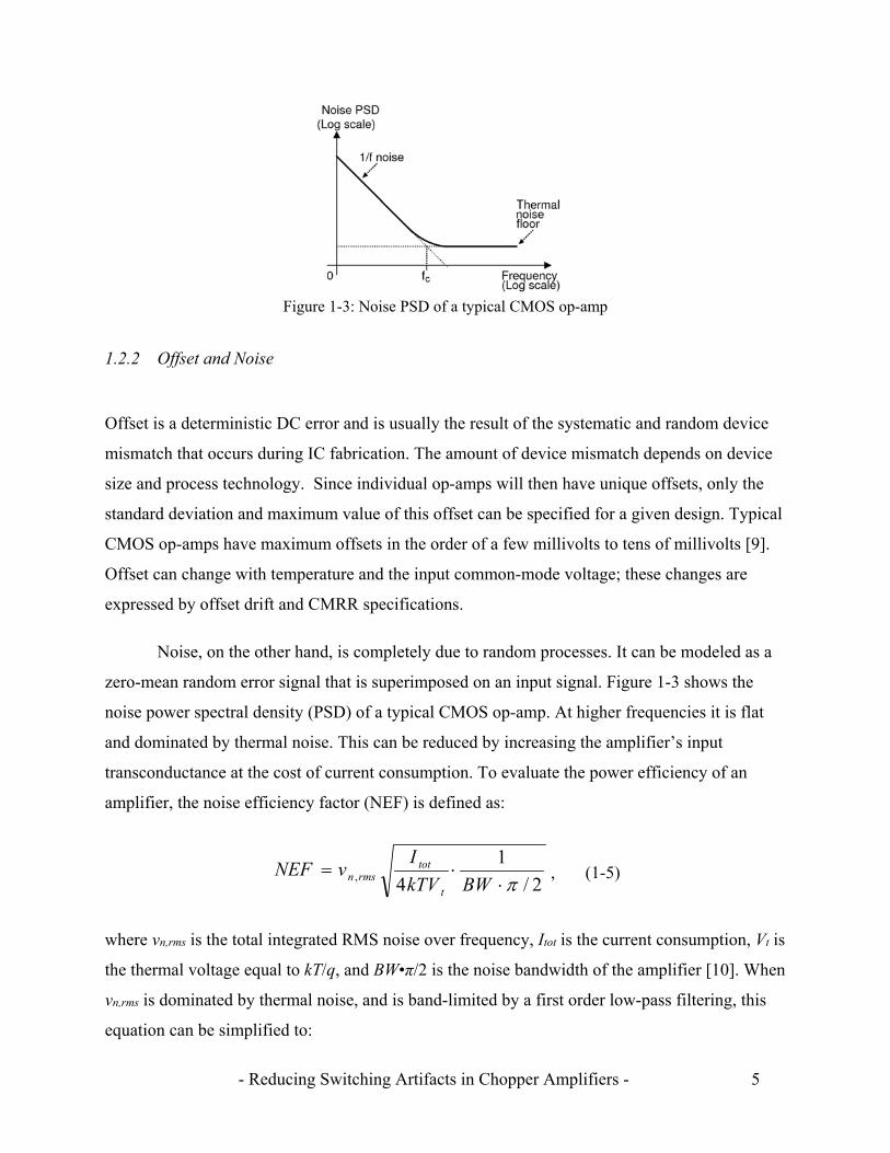
Noise, on the other hand, is completely due to random processes. It can be modeled as a
zero-mean random error signal that is superimposed on an input signal. Figure 1-3 shows the
noise power spectral density (PSD) of a typical CMOS op-amp. At higher frequencies it is flat
and dominated by thermal noise. This can be reduced by increasing the amplifier’s input
transconductance at the cost of current consumption. To evaluate the power efficiency of an
amplifier, the noise efficiency factor (NEF) is defined as:
2/
1
4,
BWkTV
IvNEF
t
totrmsn , (1-5)
where vn,rms is the total integrated RMS noise over frequency, Itot is the current consumption, Vt is
the thermal voltage equal to kT/q, and BW•π/2 is the noise bandwidth of the amplifier [10]. When
vn,rms is dominated by thermal noise, and is band-limited by a first order low-pass filtering, this
equation can be simplified to:
Figure 1-3: Noise PSD of a typical CMOS op-amp
- Reducing Switching Artifacts in Chopper Amplifiers - 6
t
totn kTV
IeNEF
4 , (1-6)
where en is the input noise PSD. A differential pair realized by two bipolar transistors with no 1/f
noise has an NEF of unity. On the other hand, a CMOS op-amp usually has a higher NEF due to
various factors: the presence of more than one dominant noise source in its input stage; the
current consumption of the subsequent gain stages; and the fact that for the same current the
thermal noise of a MOS transistor is higher than that of a bipolar transistor. At lower frequencies,
the noise PSD is dominated by 1/f noise, which increases as the frequency decreases [5]. The
amount of 1/f noise and hence the corner frequency fc depend on the device size and the process
technology. Typical CMOS op-amps have corner frequencies in the range of a few kilohertz to
tens of kilohertz.
1.2.3 Summary
CMOS op-amps suffer from considerable offset and 1/f noise which dominates their overall error
in low frequency applications. Although such errors can be reduced by increasing device sizes,
this will increase chip area and hence production cost. Offset can also be reduced by post-
production trimming. However, this will usually not compensate well for offset drift over
temperature. For these reasons, most precision op-amps have been realized in bipolar processes
which offer lower offset and 1/f noise than CMOS processes. On the other hand, CMOS op-amps
have a number of advantages, and thus are gaining popularity. First, most precision ADCs and
digital processors are realized in CMOS processes, and so can be co-integrated with CMOS op-
amps. Second, CMOS wafers are cheaper than bipolar or JFET ones. Third, digital logic and
analog switches can be easily implemented in CMOS processes, enabling the use of various
dynamic error correction techniques. Specifically, dynamic offset cancellation techniques such as
auto-zeroing and chopping, can reduce offset and offset drift to levels significantly lower than
those of trimmed bipolar op-amps [11]. Thus, chopper and auto-zero op-amps in CMOS
processes have successfully served applications requiring microvolt-level offset, very low
temperature drift, and/or low 1/f noise [11].
- Reducing Switching Artifacts in Chopper Amplifiers - 7
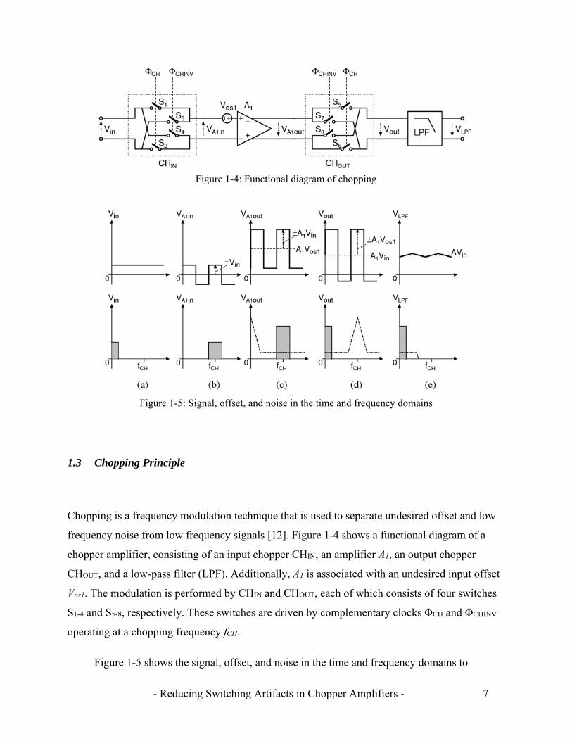
1.3 Chopping Principle
Chopping is a frequency modulation technique that is used to separate undesired offset and low
frequency noise from low frequency signals [12]. Figure 1-4 shows a functional diagram of a
chopper amplifier, consisting of an input chopper CHIN, an amplifier A1, an output chopper
CHOUT, and a low-pass filter (LPF). Additionally, A1 is associated with an undesired input offset
Vos1. The modulation is performed by CHIN and CHOUT, each of which consists of four switches
S1-4 and S5-8, respectively. These switches are driven by complementary clocks ΦCH and ΦCHINV
operating at a chopping frequency fCH.
Figure 1-5 shows the signal, offset, and noise in the time and frequency domains to
Figure 1-4: Functional diagram of chopping
Figure 1-5: Signal, offset, and noise in the time and frequency domains

- Reducing Switching Artifacts in Chopper Amplifiers - 8
illustrate how they are modulated. A low frequency input signal Vin, shown in Figure 1-5 (a), is
first up-modulated to fCH by CHIN (Figure 1-5 (b)). Next, A1 amplifies the up-modulated signal
along with the offset and noise (Figure 1-5 (c)). This up-modulated signal and the thermal noise
around fCH are then down-modulated back to baseband by CHOUT. Meanwhile, CHOUT up-
modulates the offset and the low frequency noise to fCH, and thus produces switching artifacts
(Figure 1-5 (d)). The LPF attenuates the switching artifacts, so that in the low frequency signal
only the thermal noise floor interferes (Figure 1-5 (e)). However, the cutoff frequency of the LPF
needs to be set lower than fCH, which limits the usable signal bandwidth.
1.4 Traditional Applications of Chopper Op-Amps
As explained in the previous section, chopping up-modulates low frequency errors and produces
switching artifacts. Thus, this technique has traditionally been used in low frequency
applications, where offset and 1/f noise must be low, but in which high frequency noise can be
attenuated by low-pass filters. This section reviews traditional applications of chopper op-amps
along with the required performance.
1.4.1 Sensor Signal Conditioning
Sensors convert physical signals, such as light, sound, temperature, pressure, magnetic field,
force, into electrical signals [13]. These electrical signals can be in the form of voltages, currents,
resistances, or other quantities that are often quite small. Therefore, a front-end amplifier is
required to produce a voltage output with an amplitude that is compatible with the full scale
input of the ADC. Figure 1-6 shows a circuit diagram consisting of an op-amp and two gain
setting resistors RF, to amplify a bridge sensor signal [13]. The physical signal of interest is
converted into a resistance change ΔR in a resistive sensor RS. Consequently, the front-end
amplifier produces an output voltage Vout given by:
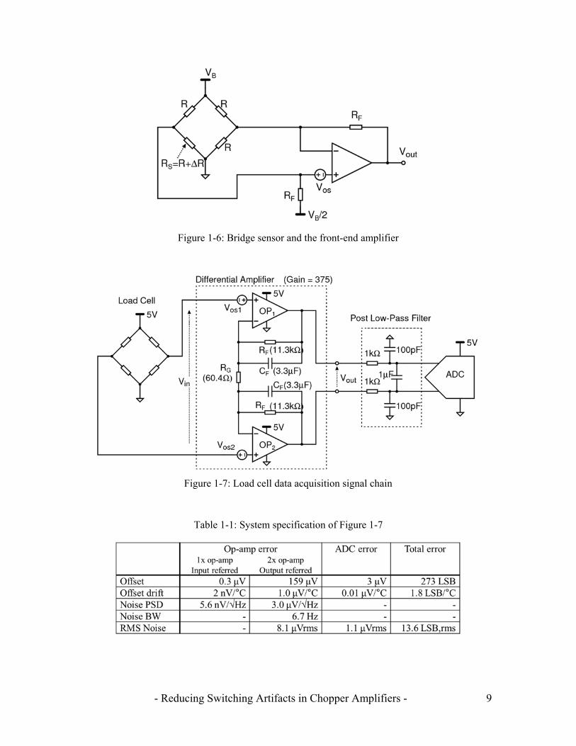
- Reducing Switching Artifacts in Chopper Amplifiers - 9
Figure 1-6: Bridge sensor and the front-end amplifier
Figure 1-7: Load cell data acquisition signal chain
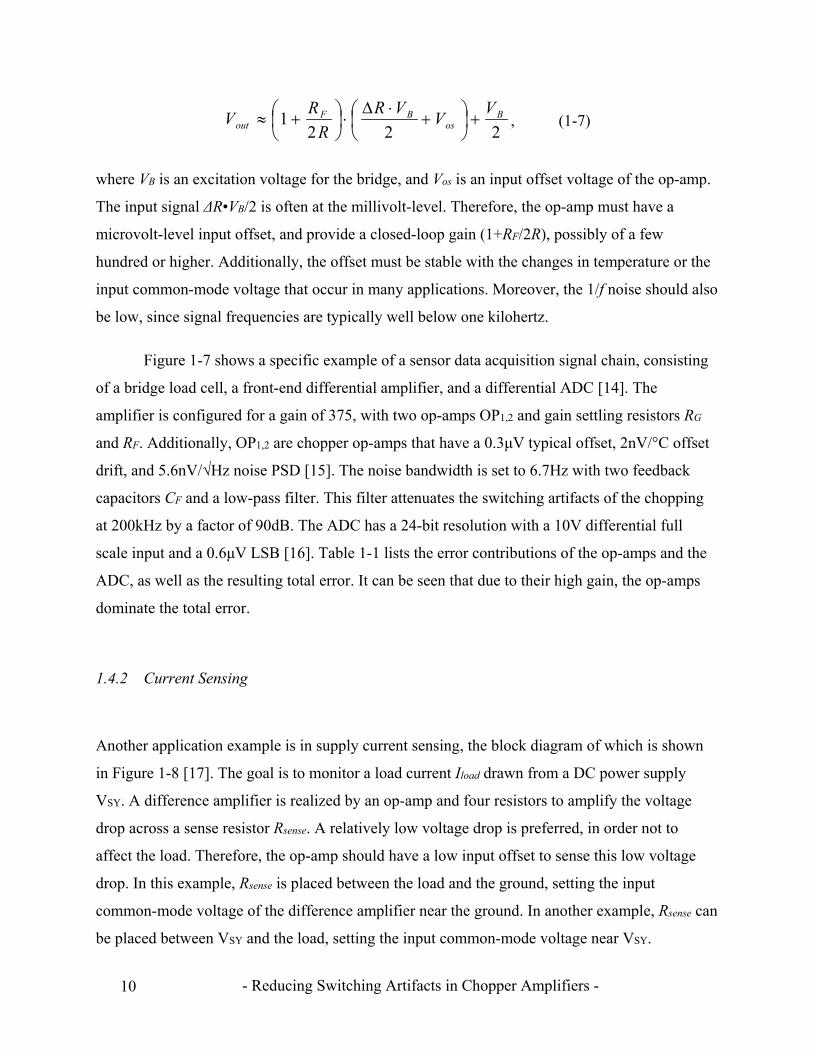
Table 1-1: System specification of Figure 1-7
- Reducing Switching Artifacts in Chopper Amplifiers - 10
2221 B
osBF
out
VV
VR
R
RV
, (1-7)
where VB is an excitation voltage for the bridge, and Vos is an input offset voltage of the op-amp.
The input signal ΔR•VB/2 is often at the millivolt-level. Therefore, the op-amp must have a
microvolt-level input offset, and provide a closed-loop gain (1+RF/2R), possibly of a few
hundred or higher. Additionally, the offset must be stable with the changes in temperature or the
input common-mode voltage that occur in many applications. Moreover, the 1/f noise should also
be low, since signal frequencies are typically well below one kilohertz.
Figure 1-7 shows a specific example of a sensor data acquisition signal chain, consisting
of a bridge load cell, a front-end differential amplifier, and a differential ADC [14]. The
amplifier is configured for a gain of 375, with two op-amps OP1,2 and gain settling resistors RG
and RF. Additionally, OP1,2 are chopper op-amps that have a 0.3μV typical offset, 2nV/°C offset
drift, and 5.6nV/√Hz noise PSD [15]. The noise bandwidth is set to 6.7Hz with two feedback
capacitors CF and a low-pass filter. This filter attenuates the switching artifacts of the chopping
at 200kHz by a factor of 90dB. The ADC has a 24-bit resolution with a 10V differential full
scale input and a 0.6μV LSB [16]. Table 1-1 lists the error contributions of the op-amps and the
ADC, as well as the resulting total error. It can be seen that due to their high gain, the op-amps
dominate the total error.
1.4.2 Current Sensing
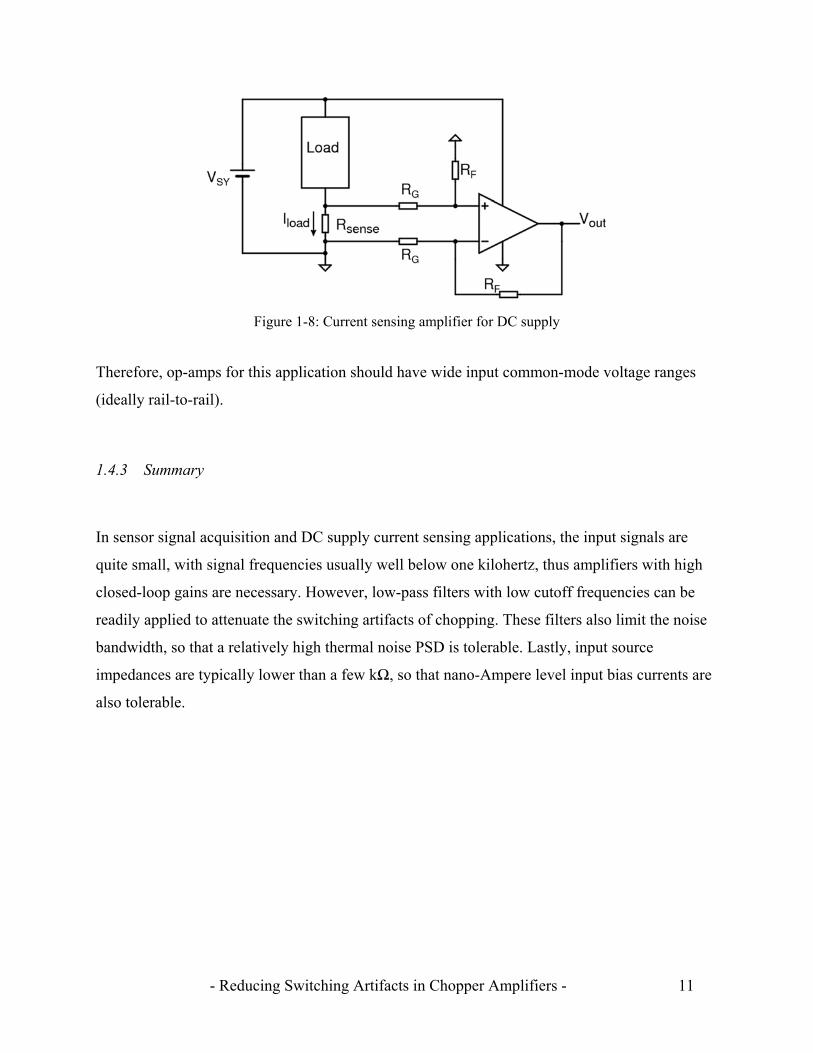
Another application example is in supply current sensing, the block diagram of which is shown
in Figure 1-8 [17]. The goal is to monitor a load current Iload drawn from a DC power supply
VSY. A difference amplifier is realized by an op-amp and four resistors to amplify the voltage
drop across a sense resistor Rsense. A relatively low voltage drop is preferred, in order not to
affect the load. Therefore, the op-amp should have a low input offset to sense this low voltage
drop. In this example, Rsense is placed between the load and the ground, setting the input
common-mode voltage of the difference amplifier near the ground. In another example, Rsense can
be placed between VSY and the load, setting the input common-mode voltage near VSY.
- Reducing Switching Artifacts in Chopper Amplifiers - 11
Therefore, op-amps for this application should have wide input common-mode voltage ranges
(ideally rail-to-rail).
1.4.3 Summary
In sensor signal acquisition and DC supply current sensing applications, the input signals are
quite small, with signal frequencies usually well below one kilohertz, thus amplifiers with high
closed-loop gains are necessary. However, low-pass filters with low cutoff frequencies can be
readily applied to attenuate the switching artifacts of chopping. These filters also limit the noise
bandwidth, so that a relatively high thermal noise PSD is tolerable. Lastly, input source
impedances are typically lower than a few kΩ, so that nano-Ampere level input bias currents are
also tolerable.
Figure 1-8: Current sensing amplifier for DC supply
- Reducing Switching Artifacts in Chopper Amplifiers - 12
1.5 Newer Applications of Chopper Op-Amps
As discussed in the previous section, chopper op-amps mainly serve applications where signal
frequencies and signal source impedances are relatively low. However, a broader range of
applications could be served, if the switching artifacts of chopping could be pushed to higher
frequencies and/or if their magnitudes could be reduced. This section introduces some new
applications that have previously been served by precision bipolar or JFET op-amps. It also
discusses the extra requirements that chopper op-amps will have to meet to serve these
applications, which form the main motivation for the work in this thesis.
1.5.1 Biomedical Sensing Front-End
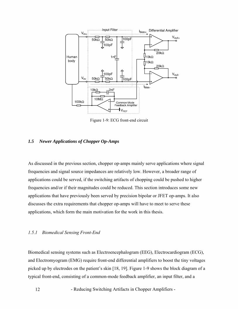
Biomedical sensing systems such as Electroencephalogram (EEG), Electrocardiogram (ECG),
and Electromyogram (EMG) require front-end differential amplifiers to boost the tiny voltages
picked up by electrodes on the patient’s skin [18, 19]. Figure 1-9 shows the block diagram of a
typical front-end, consisting of a common-mode feedback amplifier, an input filter, and a
Figure 1-9: ECG front-end circuit
- Reducing Switching Artifacts in Chopper Amplifiers - 13
differential amplifier. Since the bandwidth of these biomedical signals is about 200Hz, chopper
op-amps with low 1/f noise are preferred, and an external low-pass filter can be applied to
attenuate the switching artifacts at the chopping frequency. However, as will be explained later,
due to their input switching, chopper op-amps have input bias currents Ibias+ and Ibias–. In
conjunction with the 100kΩ input filter resistors required for patient isolation, this can cause
significant errors. For instance, a 1nA bias current mismatch will cause a 100µV differential
input offset. To avoid such large errors, the input bias currents should be at the 100pA level or
lower. Moreover, for portable and wearable applications, each op-amp should have a low power
consumption under 100 microwatts, and fit into a small package such as SC-70. Furthermore, a
wide supply voltage range including 1.8V is preferred in order to share the supply voltage with
other components such as ADCs and digital processors.
1.5.2 Reference and DAC Buffers
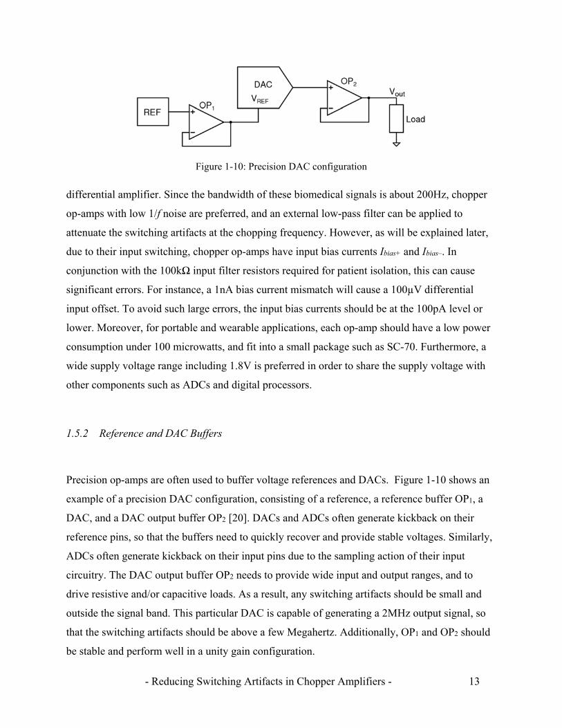
Precision op-amps are often used to buffer voltage references and DACs. Figure 1-10 shows an
example of a precision DAC configuration, consisting of a reference, a reference buffer OP1, a
DAC, and a DAC output buffer OP2 [20]. DACs and ADCs often generate kickback on their
reference pins, so that the buffers need to quickly recover and provide stable voltages. Similarly,
ADCs often generate kickback on their input pins due to the sampling action of their input
circuitry. The DAC output buffer OP2 needs to provide wide input and output ranges, and to
drive resistive and/or capacitive loads. As a result, any switching artifacts should be small and
outside the signal band. This particular DAC is capable of generating a 2MHz output signal, so
that the switching artifacts should be above a few Megahertz. Additionally, OP1 and OP2 should
be stable and perform well in a unity gain configuration.
Figure 1-10: Precision DAC configuration
- Reducing Switching Artifacts in Chopper Amplifiers - 14
1.5.3 Process Control Data Acquisition Signal Chain
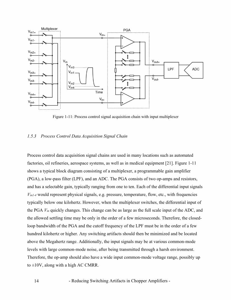
Process control data acquisition signal chains are used in many locations such as automated
factories, oil refineries, aerospace systems, as well as in medical equipment [21]. Figure 1-11
shows a typical block diagram consisting of a multiplexer, a programmable gain amplifier
(PGA), a low-pass filter (LPF), and an ADC. The PGA consists of two op-amps and resistors,
and has a selectable gain, typically ranging from one to ten. Each of the differential input signals
Vin1-4 would represent physical signals, e.g. pressure, temperature, flow, etc., with frequencies
typically below one kilohertz. However, when the multiplexer switches, the differential input of
the PGA Vin quickly changes. This change can be as large as the full scale input of the ADC, and
the allowed settling time may be only in the order of a few microseconds. Therefore, the closed-
loop bandwidth of the PGA and the cutoff frequency of the LPF must be in the order of a few
hundred kilohertz or higher. Any switching artifacts should then be minimized and be located
above the Megahertz range. Additionally, the input signals may be at various common-mode
levels with large common-mode noise, after being transmitted through a harsh environment.
Therefore, the op-amp should also have a wide input common-mode voltage range, possibly up
to ±10V, along with a high AC CMRR.
Figure 1-11: Process control signal acquisition chain with input multiplexer

- Reducing Switching Artifacts in Chopper Amplifiers - 15
1.6 Challenges
The previous sections discussed traditional applications of chopper op-amps, as well as some
newer ones. To justify their development costs, chopper op-amp designs should cover as many of
these applications as possible. This is especially true for a stand-alone op-amp IC or an op-amp
IP core intended for use in a variety of other ICs. Such a chopper op-amp should have small
switching artifacts located at higher frequencies, while achieving low offset and low 1/f noise.
Additionally, a low noise PSD, wide supply range, and wide common-mode voltage range will
allow the op-amp to be used in a broader range of applications.
The chopping frequency should be set high enough to extend the usable signal bandwidth
and to cover the newer applications. However, apart from the traditional op-amp design trade-
offs between noise PSD, current consumption, and die area, chopper op-amp design also
involves specific trade-offs between noise PSD, chopping frequency, and residual offset, caused
by the switching artifacts.
1.7 Organization of the Thesis
This thesis presents circuit techniques that reduce the switching artifacts in chopper amplifiers,
so as to achieve the levels of performance described in the previous section. Some of the
proposed techniques can push the noise spectra peak to higher frequencies and reduce their
magnitude, without significantly increasing the residual offset. Consequently, the proposed
chopper op-amps offer wider usable signal bandwidths as well as superb DC performance, and
therefore can be implemented in a broader range of applications.
Chapter 2 reviews three offset cancellation techniques—trimming, auto-zeroing, and
chopping—including their advantages and disadvantages. In the review of the chopping
technique, various switching artifacts are explained, including up-modulated ripple, output
glitches, residual offset and input bias current, and gain reduction due to dynamic switching
conductance. Next, Chapter 3 reviews some previous techniques that reduce some of these

- Reducing Switching Artifacts in Chopper Amplifiers - 16
switching artifacts.
Some original contributions are presented in Chapters 4, 5 and 6. Each chapter presents
an individual design project, along with the proposed techniques, the overall op-amp design, and
the measurement results. In Chapter 4, a local feedback technique, called auto-correction
feedback (ACFB) is proposed to reduce the up-modulated ripple. This technique is implemented
in a low power chopper op-amp design that draws 13µA from a 1.8 to 5.5V supply, to serve low
power applications.
Chapter 5 presents a chopper op-amp that achieves a 5.6nV/√Hz noise PSD and a 0.5µV
maximum offset, to serve applications requiring very small low frequency error. In order to
mitigate the trade-off between the noise PSD and the residual offset, an adaptive clock boosting
technique is employed in the input chopper. This minimizes its charge injection and keeps it
constant over the amplifier’s rail-to-rail input common-mode voltage range.
Chapter 6 presents a chopper op-amp, which operates from a 4.5-60V supply, and is
intended to serve industrial applications that require wide supply and input common-mode
voltage ranges as well as wide usable signal bandwidth. Two techniques are proposed to locate
switching artifacts at higher frequencies and to reduce their magnitude. First, this op-amp
employs six parallel input stages driven by 800kHz interleaved clocks, so as to locate the
majority of the switching energy at 4.8MHz. Second, the input chopper incorporates a charge
mismatch compensation circuit to reduce the maximum input bias current from 1.5nA to 150pA
at post-production trimming. The thesis ends with Chapter 7, in which its original contributions
are reviewed and the performance of the various designs is compared with the state-of-the-art.
- Reducing Switching Artifacts in Chopper Amplifiers - 17
1.8 References
[1] J. Bradley, J. Barbier, and D. Handler, “Embracing the Internet of Everything To Capture
Your Share of $14.4 Trillion”, Cisco Systems, 2013, Accessed on March 2018, [Online]
Available: <http://www.cisco.com/web/about/ac79/docs/innov/IoE_Economy.pdf>.
[2] B. Bateman, “IoT is driving an analog opportunity”, EE Times, May 2015, Accessed on
March 2018, [Online] Available: <http://www.electronics-eetimes.com/en/iot-is-driving-an-
analog-opportunity.html?cmp_id=7&news_id=222924930>.
[3] M. Pachchigar, “Low Power Precision Data Acquisition Signal Chain for Space Constrained
Applications”, Accessed on March 2018, [Online] Available:
<http://www.analog.com/media/en/technical-documentation/technical-articles/Low-Power-
Precision-Data-Acquisition-Signal-Chain-for-Space-Constrained-Applications.pdf>.
[4] Texas Instruments, “AN-31 Op Amp Circuit Collection”, May 2013, Accessed on March
2018, [Online] Available: <http://www.ti.com/lit/an/snla140b/snla140b.pdf>.
[5] B. Razavi, “Design of Analog CMOS Integrated Circuits”, McGraw Hill Companies, Inc.,
2001.
[6] W. Sansen, Analog Design Essentials, Springer, Dordrecht, the Netherlands, 2006.
[7] J. H. Huijsing, Operational Amplifier Theory and Design, 2nd Edition, Springer, 2011.
[8] Analog Devices, “MT-054 Tutorial, Precision Op Amps”, Accessed on March 2018, [Online]
Available: <http://www.analog.com/media/en/training-seminars/tutorials/MT-054.pdf>.
[9] Analog Devices, “MT-037 Tutorial, Op Amp Input Offset Voltage”, Accessed on March
2018, [Online] Available: <http://www.analog.com/media/en/training-seminars/tutorials/MT-
037.pdf>.
- Reducing Switching Artifacts in Chopper Amplifiers - 18
[10] M. S. J. Steyaert, W. M. C. Sansen, and C. Zhongyuan, “A Micropower Low-Noise
Monolithic Instrumentation Amplifier For Medical Purposes”, IEEE J. Solid-State Circuits, vol.
22, no. 6, pp. 1163-1168, Dec. 1987.
[11] Analog Devices, “MT-055 Tutorial, Chopper Stabilized (Auto-Zero) Precision Op Amps”,
Accessed on March 2018, [Online] Available: <http://www.analog.com/media/en/training-
seminars/tutorials/MT-055.pdf>.
[12] C. C. Enz and G. C. Temes, “Circuit Techniques for Reducing the Effect of Op-Amp
Imperfections: Autozeroing, Correlated Double Sampling, and Chopper Stabilization”, Proc. of
IEEE, vol. 84, no. 9, pp. 1320-1324, Sept. 1996.
[13] W. Kester, J. Bryant, and W. Jung, “Amplifiers for Signal Conditioning, Section 3”, 1999,
Accessed on March 2018, [Online] Available: <http://www.analog.com/media/en/training-
seminars/design-handbooks/sensor-signal-cond-sect3.PDF>.
[14] Analog Devices, “CN-0216: Precision Weigh Scale Design Using the AD7791 24-Bit
Sigma-Delta ADC with External ADA4528-1 Zero-Drift Amplifiers”, Sept. 2011, Accessed on
March 2018, [Online] Available: <http://www.analog.com/media/en/reference-design-
documentation/reference-designs/CN0216.pdf>.
[15] Analog Devices, “ADA4528 Datasheet”, Jan. 2011, Accessed on March 2018, [Online]
Available: <http://www.analog.com/media/en/technical-documentation/data-sheets/ADA4528-
1_4528-2.pdf>.
[16] Analog Devices, “AD7791 Datasheet”, Aug. 2003, Accessed on March 2018, [Online]
Available: <http://www.analog.com/media/en/technical-documentation/data-
sheets/AD7791.pdf>.
[17] N. Zhao, W. Liao, and H. Sino, “High-Side Current Sensing with Wide Dynamic Range:
Three Solutions”, Dec. 2010, Accessed on March 2018, [Online] Available:
<http://www.analog.com/library/analogDialogue/archives/44-12/high_side.html>.

- Reducing Switching Artifacts in Chopper Amplifiers - 19
[18] M. W. Hann, “Ultra Low Power, 18 bit Precision ECG Data Acquisition System”, June
2013, Accessed on March 2018, [Online] Available:
<http://www.ti.com/lit/ug/slau516/slau516.pdf>.
[19] R. F. Yazicioglu, P. Merken, R. Puers, and C. V. Hoof, “A 60 W 60 nV/√Hz Readout
Front-End for Portable Biopotential Acquisition Systems”, IEEE J. Solid-State Circuits, vol. 42,
no. 5, pp. 1100-1110, May 2007.
[20] Analog Devices, “CN-0181: Precision, 16-Bit, Voltage Level Setting with Less than 5 mW
Total Power Dissipation”, Mar. 2011, Accessed on March 2018, [Online] Available:
<http://www.analog.com/media/en/reference-design-documentation/reference-
designs/CN0181.pdf>.
[21] M. Pachchigar, “Complete Sensor-to-Bits Solution Simplifies Industrial Data-Acquisition
System Design”, Apr. 2013, Accessed on March 2018, [Online] Available:
<http://www.analog.com/library/analogdialogue/archives/47-04/sensor_to_bits.html>.
- Reducing Switching Artifacts in Chopper Amplifiers - 20
- Reducing Switching Artifacts in Chopper Amplifiers - 21
Chapter 2
Offset Cancellation Techniques
This chapter reviews offset cancellation techniques for amplifiers. First to be reviewed is offset
trimming, in which offset is measured and then corrected at post-production test. Since the
correction is performed only once, offset drift over time and temperature usually remains
uncorrected. Next, after an explanation of the properties of MOS switches, a review is presented
of dynamic offset cancellation techniques, such as auto-zeroing and chopping. Unlike offset
trimming, these techniques periodically correct offset, and thus reduce offset drift and 1/f noise.
However, as will be discussed, these techniques also have drawbacks, which include various
residual DC and AC errors.
- Reducing Switching Artifacts in Chopper Amplifiers - 22
2.1 Offset Trimming
Offset trimming involves measuring the offset and then subtracting the resulting value thereafter
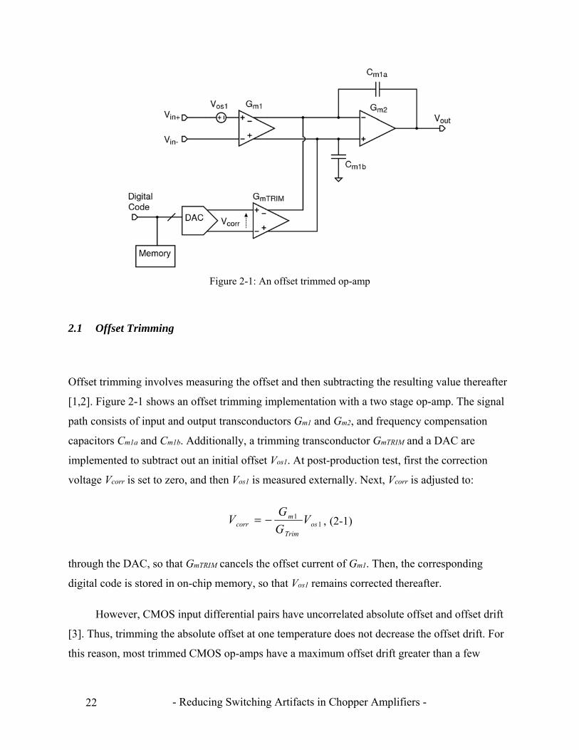
[1,2]. Figure 2-1 shows an offset trimming implementation with a two stage op-amp. The signal
path consists of input and output transconductors Gm1 and Gm2, and frequency compensation
capacitors Cm1a and Cm1b. Additionally, a trimming transconductor GmTRIM and a DAC are
implemented to subtract out an initial offset Vos1. At post-production test, first the correction
voltage Vcorr is set to zero, and then Vos1 is measured externally. Next, Vcorr is adjusted to:
11
osTrim
mcorr V
G
GV , (2-1)
through the DAC, so that GmTRIM cancels the offset current of Gm1. Then, the corresponding
digital code is stored in on-chip memory, so that Vos1 remains corrected thereafter.
However, CMOS input differential pairs have uncorrelated absolute offset and offset drift
[3]. Thus, trimming the absolute offset at one temperature does not decrease the offset drift. For
this reason, most trimmed CMOS op-amps have a maximum offset drift greater than a few
Figure 2-1: An offset trimmed op-amp

- Reducing Switching Artifacts in Chopper Amplifiers - 23
µV/°C [4]. In 2011, Bolatkale reported a MOS-input op-amp achieving a 0.33µV/°C maximum
offset drift by biasing the input stage at two different currents, while trimming at one temperature
[3]. However, the second gain stage uses complementary bipolar devices which are not available
in every CMOS process. In 2013, another MOS-input op-amp achieving a 0.8µV/°C maximum
offset drift was reported [5], where its offset is corrected at the ambient temperature by a first
DAC, and then its offset drift over temperature is corrected at a higher temperature by a second
DAC. However, this method requires offset measurements at two different temperatures for each
op-amp unit, and thus increases production cost. Bipolar input differential pairs have correlated
absolute offset and offset drift, and therefore can achieve lower offset drift. For instance, the one
reported in [6] achieves a 0.25µV/°C maximum offset drift. Nevertheless, as discussed in Section
1.4.1, this level of offset drift is still insufficient in some sensor applications, which require
offset drifts below 0.1 µV/°C. Additionally, bipolar op-amps are ruled out in some applications
due to their high input bias current (several nano-Amperes) and high manufacturing cost.
2.2 MOS Switches
2.2.1 Realization and On-Resistance
This section explains the properties of the MOS switches that are used in the dynamic offset
cancellation techniques. They can be realized by either NMOS or PMOS switches, or a
Figure 2-2: (a) An NMOS switch and (b) the on-conductance versus input voltage
- Reducing Switching Artifacts in Chopper Amplifiers - 24
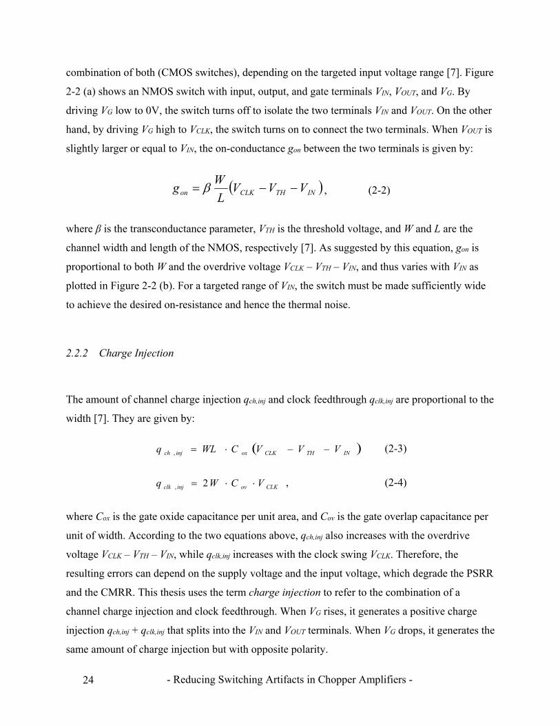
combination of both (CMOS switches), depending on the targeted input voltage range [7]. Figure
2-2 (a) shows an NMOS switch with input, output, and gate terminals VIN, VOUT, and VG. By
driving VG low to 0V, the switch turns off to isolate the two terminals VIN and VOUT. On the other
hand, by driving VG high to VCLK, the switch turns on to connect the two terminals. When VOUT is
slightly larger or equal to VIN, the on-conductance gon between the two terminals is given by:
INTHCLKon VVVL
Wg , (2-2)
where β is the transconductance parameter, VTH is the threshold voltage, and W and L are the
channel width and length of the NMOS, respectively [7]. As suggested by this equation, gon is
proportional to both W and the overdrive voltage VCLK – VTH – VIN, and thus varies with VIN as
plotted in Figure 2-2 (b). For a targeted range of VIN, the switch must be made sufficiently wide
to achieve the desired on-resistance and hence the thermal noise.
2.2.2 Charge Injection
The amount of channel charge injection qch,inj and clock feedthrough qclk,inj are proportional to the
width [7]. They are given by:
INTHCLKoxinjch VVVCWLq , (2-3)
CLKovinjclk VCWq 2, , (2-4)
where Cox is the gate oxide capacitance per unit area, and Cov is the gate overlap capacitance per
unit of width. According to the two equations above, qch,inj also increases with the overdrive
voltage VCLK – VTH – VIN, while qclk,inj increases with the clock swing VCLK. Therefore, the
resulting errors can depend on the supply voltage and the input voltage, which degrade the PSRR
and the CMRR. This thesis uses the term charge injection to refer to the combination of a
channel charge injection and clock feedthrough. When VG rises, it generates a positive charge
injection qch,inj + qclk,inj that splits into the VIN and VOUT terminals. When VG drops, it generates the
same amount of charge injection but with opposite polarity.
- Reducing Switching Artifacts in Chopper Amplifiers - 25
2.2.3 Cancellation of Charge Injection
To cancel the charge injection of an NMOS switch S1, a PMOS switch S2 can be added as shown
in Figure 2-3 (a). S1 and S2 are driven by two complementary clocks Φ1 and Φ2, respectively. As
a result, the switches generate charge injection of opposite polarity that cancel each other out.
However, this cancellation scheme only works when VIN is exactly half of VCLK. Otherwise, the
two switches have unequal overdrive voltages, and thus generate unequal amounts of channel
charge injection.
Another way to cancel charge injection is to add an NMOS dummy switch S2 as shown in
Figure 2-3 (b). S2 is half the size of S1, so that its charge injections qs2 and qd2 cancel that of S1
(qd1) at the VOUT node. However, the VIN and VOUT nodes are often driven by unequal
impedances. In this case, the overall charge injection of S1 is unequally split between these
nodes, making this cancellation scheme ineffective.
The most effective solution is to use differential circuitry as shown in Figure 2-3 (c). Two
NMOS switches S1 and S2 are driven by a single clock Φ1, generating a nearly equal amount of
charge injection. As long as the impedances are balanced differentially, the charge injection
mismatch is only due to coupling capacitance mismatch, which is in the order of 1% to 10%.
As will be explained later, charge injection causes DC residual offset and transient glitches
Figure 2-3: Cancellation of charge injection by (a) complementary switch, (b) dummy switch, and (c) differential circuitry

- Reducing Switching Artifacts in Chopper Amplifiers - 26
in either chopper or auto-zero amplifiers. The residual offset is proportional to the amount of
charge injection mismatch between differential switches. On the other hand, the magnitude of the
glitches mainly depends on the absolute amount of charge injection. Therefore, both the
mismatch and the absolute amount of charge injection should be minimized, while meeting the
targeted on-resistance, and hence the thermal noise PSD.
Figure 2-4: An auto-zero op-amp

- Reducing Switching Artifacts in Chopper Amplifiers - 27
2.3 Auto-Zeroing
Auto-zeroing is one of the two dynamic offset cancellation techniques available. Unlike offset
trimming, it periodically measures and corrects offset, and thus reduces the offset drift and 1/f
noise as well [7,8].
2.3.1 Principle
A block diagram of a two stage, auto-zeroed op-amp is shown in Figure 2-4. The signal path
consists of input and output transconductors Gm1 and Gm2. Additionally, it implements switches
S1-8, sampling capacitors CAZ1,2, and an auto-zeroing transconductor GmAZ, to measure, sample,
and cancel an input offset of Gm1 (Vos1). Switches S1-8 are driven by complementary clocks ΦAZ
and ΦAZINV, operating at the auto-zeroing frequency fAZ. The op-amp is in the auto-zero phase
when ΦAZ is high, and is in the amplification phase when ΦAZINV is high. In the auto-zero phase,
the differential inputs of Gm1 are shorted to a common-mode voltage VCM, and the outputs are
connected to the inputs of GmAZ to form a local auto-zeroing feedback loop. Assuming the loop
gain is infinite, the offset correction voltage Vcorr is adjusted to:
11
osmAZ
mcorr V
G
GV , (2-5)
so that GmAZ cancels Vos1. When ΦAZ drops, Vcorr is sampled by CAZ1,2. Next, when the
amplification phase begins, the differential inputs and outputs of Gm1 are connected to the signal
path, so that the op-amp can amplify the input signals. The resulting offset is zero in principle,
since Vos1 is still cancelled by GmAZ with the sampled Vcorr in the previous auto-zero phase.
2.3.2 Residual Offset
In the circuit of Figure 2-4, residual offset is the result of several imperfections [7]. First, the
- Reducing Switching Artifacts in Chopper Amplifiers - 28
auto-zeroing feedback has a finite loop gain AvAZ, resulting in an error voltage. Second, GmAZ also
has an input offset VosAZ. Third, sampling switches S7 and S8 generate charge injections q7 and q8,
when turning off. Their charge injection mismatch ΔqAZ8,7 = qAZ8 – qAZ7 then flows into CAZ1,2,
and produces another error voltage. As a result, the correction voltage Vcorr includes the
combined error voltage Vcorrerr equaling:
2,1
7,81
11
AZosAZos
mAZ
m
vAZcorrerr C
qVV
G
G
AV
. (2-6)
By multiplying this error by GmAZ/Gm1, the residual input offset Vos,res obtained is:
2,1
7,8
111,
1
AZm
mAZosAZ
m
mAZos
vAZresos C
q
G
GV
G
GV
AV
. (2-7)
To minimize this residual offset, the auto-zeroing loop gain AzAZ should be increased by using a
cascoded topology. Additionally, CAZ1,2 should be increased, and GmAZ should be reduced with
respect to Gm1. However, the tail current of GmAZ must cover the maximum offset current of Gm1.
Therefore, the transconductance should be reduced by employing long channel MOS devices or
resistor degeneration. For instance, with AvAZ = 80dB, a 10mV initial offset results in a 1µV
residual offset. Additionally, with CAZ1,2 = 10pF and GmAZ/Gm1 = 0.1, a 1fC charge injection
mismatch will produce a 10µV residual offset.
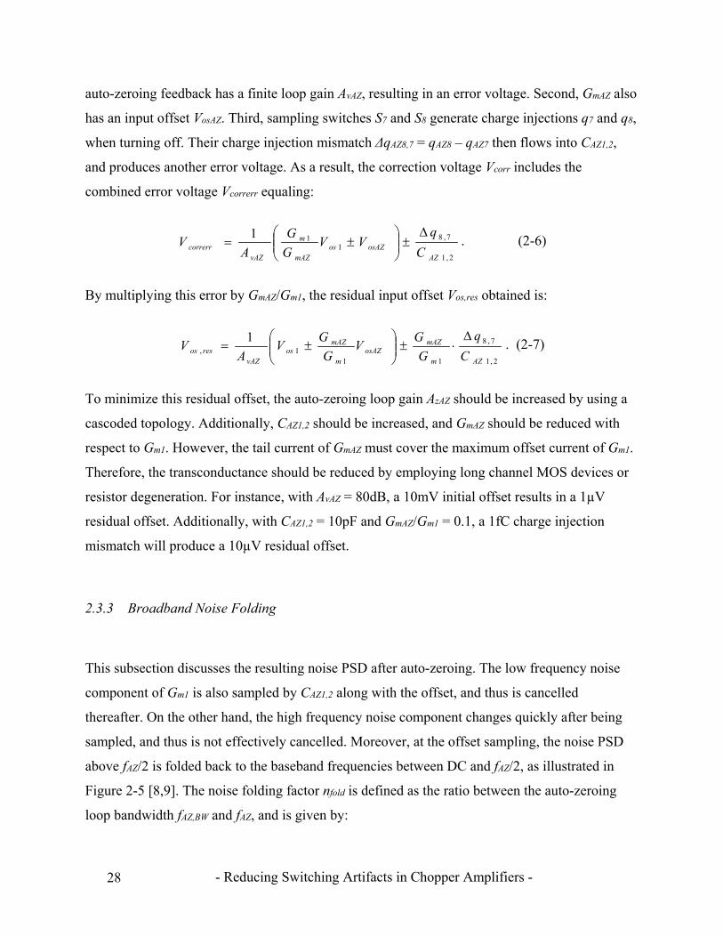
2.3.3 Broadband Noise Folding
This subsection discusses the resulting noise PSD after auto-zeroing. The low frequency noise
component of Gm1 is also sampled by CAZ1,2 along with the offset, and thus is cancelled
thereafter. On the other hand, the high frequency noise component changes quickly after being
sampled, and thus is not effectively cancelled. Moreover, at the offset sampling, the noise PSD
above fAZ/2 is folded back to the baseband frequencies between DC and fAZ/2, as illustrated in
Figure 2-5 [8,9]. The noise folding factor nfold is defined as the ratio between the auto-zeroing
loop bandwidth fAZ,BW and fAZ, and is given by:
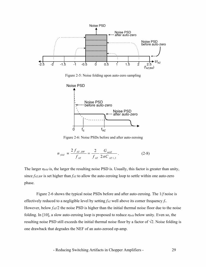
- Reducing Switching Artifacts in Chopper Amplifiers - 29
2,1
,
2
22
AZ
mAZ
AZAZ
BWAZfold C
G
ff
fn
. (2-8)
The larger nfold is, the larger the resulting noise PSD is. Usually, this factor is greater than unity,
since fAZ,BW is set higher than fAZ to allow the auto-zeroing loop to settle within one auto-zero
phase.
Figure 2-6 shows the typical noise PSDs before and after auto-zeroing. The 1/f noise is
effectively reduced to a negligible level by setting fAZ well above its corner frequency fc.
However, below fAZ/2 the noise PSD is higher than the initial thermal noise floor due to the noise
folding. In [10], a slow auto-zeroing loop is proposed to reduce nfold below unity. Even so, the
resulting noise PSD still exceeds the initial thermal noise floor by a factor of √2. Noise folding is
one drawback that degrades the NEF of an auto-zeroed op-amp.
Figure 2-5: Noise folding upon auto-zero sampling
Figure 2-6: Noise PSDs before and after auto-zeroing
- Reducing Switching Artifacts in Chopper Amplifiers - 30
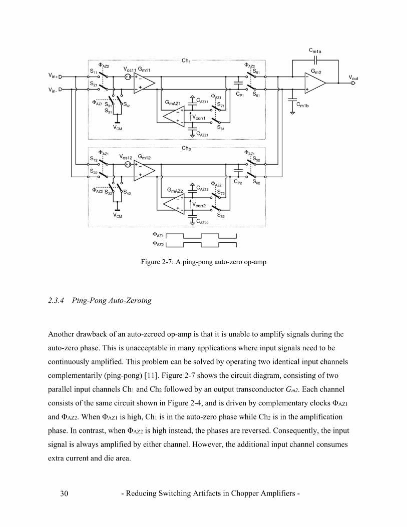
2.3.4 Ping-Pong Auto-Zeroing
Another drawback of an auto-zeroed op-amp is that it is unable to amplify signals during the
auto-zero phase. This is unacceptable in many applications where input signals need to be
continuously amplified. This problem can be solved by operating two identical input channels
complementarily (ping-pong) [11]. Figure 2-7 shows the circuit diagram, consisting of two
parallel input channels Ch1 and Ch2 followed by an output transconductor Gm2. Each channel
consists of the same circuit shown in Figure 2-4, and is driven by complementary clocks ΦAZ1
and ΦAZ2. When ΦAZ1 is high, Ch1 is in the auto-zero phase while Ch2 is in the amplification
phase. In contrast, when ΦAZ2 is high instead, the phases are reversed. Consequently, the input
signal is always amplified by either channel. However, the additional input channel consumes
extra current and die area.
Figure 2-7: A ping-pong auto-zero op-amp
- Reducing Switching Artifacts in Chopper Amplifiers - 31
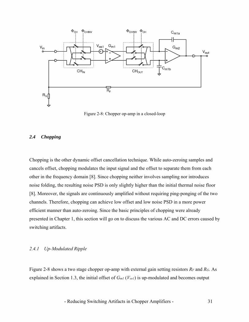
2.4 Chopping
Chopping is the other dynamic offset cancellation technique. While auto-zeroing samples and
cancels offset, chopping modulates the input signal and the offset to separate them from each
other in the frequency domain [8]. Since chopping neither involves sampling nor introduces
noise folding, the resulting noise PSD is only slightly higher than the initial thermal noise floor
[8]. Moreover, the signals are continuously amplified without requiring ping-ponging of the two
channels. Therefore, chopping can achieve low offset and low noise PSD in a more power
efficient manner than auto-zeroing. Since the basic principles of chopping were already
presented in Chapter 1, this section will go on to discuss the various AC and DC errors caused by
switching artifacts.
2.4.1 Up-Modulated Ripple
Figure 2-8 shows a two stage chopper op-amp with external gain setting resistors RF and RG. As
explained in Section 1.3, the initial offset of Gm1 (Vos1) is up-modulated and becomes output
Figure 2-8: Chopper op-amp in a closed-loop
- Reducing Switching Artifacts in Chopper Amplifiers - 32
ripple [12]. The amplitude of this ripple is affected by the closed-loop gain ACL and the closed-
loop bandwidth fCL given by:
G
FCL R
RA 1 (2-9)
bam
m
CLCL C
G
Af
,1
1
2
1
. (2-10)
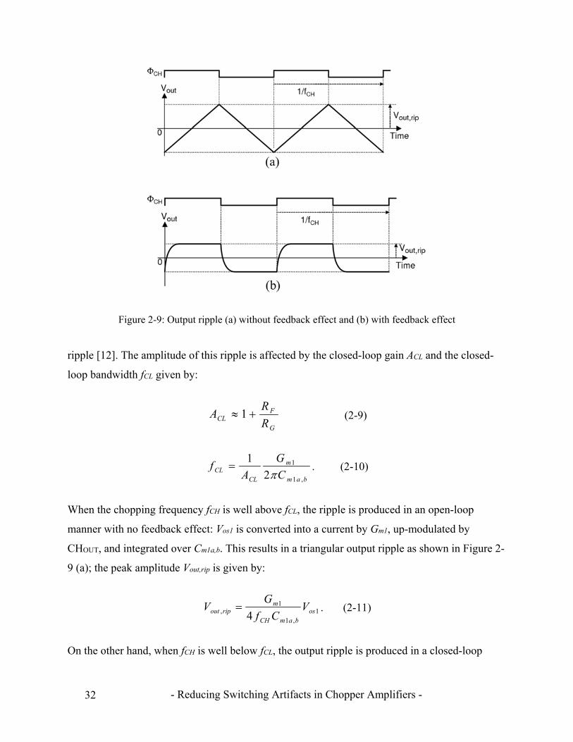
When the chopping frequency fCH is well above fCL, the ripple is produced in an open-loop
manner with no feedback effect: Vos1 is converted into a current by Gm1, up-modulated by
CHOUT, and integrated over Cm1a,b. This results in a triangular output ripple as shown in Figure 2-
9 (a); the peak amplitude Vout,rip is given by:
1,1
1, 4 os
bamCH
mripout V
Cf
GV . (2-11)
On the other hand, when fCH is well below fCL, the output ripple is produced in a closed-loop
Figure 2-9: Output ripple (a) without feedback effect and (b) with feedback effect

- Reducing Switching Artifacts in Chopper Amplifiers - 33
manner with the feedback effect. Thus, it settles to two constant voltages after every clock
transition, as shown in Figure 2-9 (b). The amplitude Vout,rip is then given by:
1, osCLripout VAV . (2-12)
For instance, with Gm1 = 100µS, Vos1 = 1mV, fCH = 100kHz, Cm1a,b = 10pF, and ACL = 100, Vout,rip
is 25mV according to (2-11). When ACL is reduced to 10 while the other parameters remain the
same, Vout,rip becomes 10mV according to (2-12). In either case, the amplitude of the ripple is
quite large, and therefore needs to be attenuated in most applications.
2.4.2 Glitches
The transient waveforms in a chopper amplifier have been drawn in Figure 2-9 (a) and (b), where
the effect of charge injection is neglected. In fact, as illustrated in Figure 2-10, charge injection
of the input switches causes output glitches [13,14]. First, ΦCH drops, injecting negative charge
on the differential input pins. Soon thereafter, ΦCHINV rises, injecting almost the same amount of
charges but with positive polarity. Ideally, these negative and positive charges cancel out
instantaneously at each input pin, if the transitions of the two clocks occur at the exact same
time. In practice, however, there must be some dead time between the two clocks, in order not to
short the differential input pins with the switches. This generates short pulses on both input pins,
resulting in an output glitch. Since this occurs in the order of a nanosecond, the op-amp is not
fast enough to suppress this glitch via its feedback loop. The glitch amplitude depends on the
Figure 2-10: Output glitch due to input charge injection
- Reducing Switching Artifacts in Chopper Amplifiers - 34
source impedances, the dead time, and the amount of charge injection. Similarly, after a half
chopping period, ΦCHINV drops and ΦCH rises, resulting in another glitch.
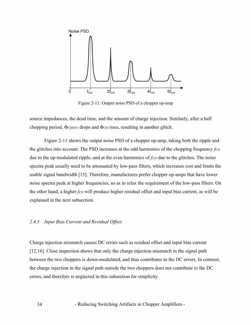
Figure 2-11 shows the output noise PSD of a chopper op-amp, taking both the ripple and
the glitches into account. The PSD increases at the odd harmonics of the chopping frequency fCH
due to the up-modulated ripple, and at the even harmonics of fCH due to the glitches. The noise
spectra peak usually need to be attenuated by low-pass filters, which increases cost and limits the
usable signal bandwidth [15]. Therefore, manufactures prefer chopper op-amps that have lower
noise spectra peak at higher frequencies, so as to relax the requirement of the low-pass filters. On
the other hand, a higher fCH will produce higher residual offset and input bias current, as will be
explained in the next subsection.
2.4.3 Input Bias Current and Residual Offset
Charge injection mismatch causes DC errors such as residual offset and input bias current
[12,16]. Close inspection shows that only the charge injection mismatch in the signal path
between the two choppers is down-modulated, and thus contributes to the DC errors. In contrast,
the charge injection in the signal path outside the two choppers does not contribute to the DC
errors, and therefore is neglected in this subsection for simplicity.
Figure 2-11: Output noise PSD of a chopper op-amp
- Reducing Switching Artifacts in Chopper Amplifiers - 35
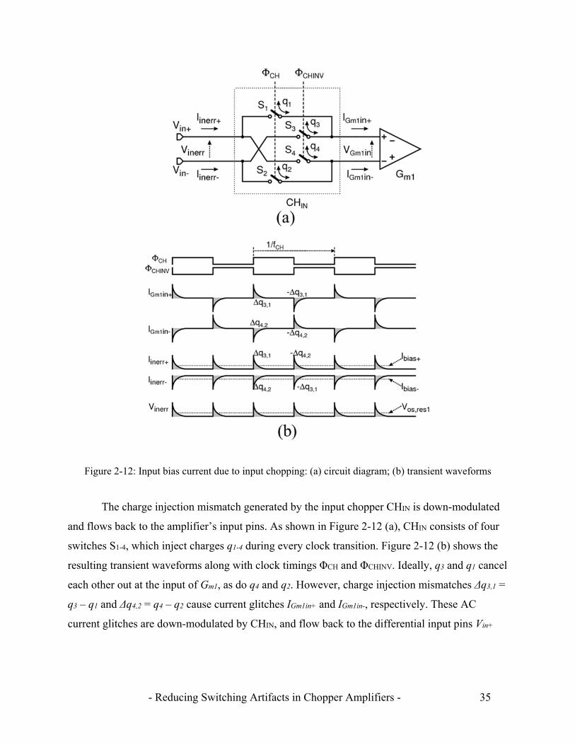
The charge injection mismatch generated by the input chopper CHIN is down-modulated
and flows back to the amplifier’s input pins. As shown in Figure 2-12 (a), CHIN consists of four
switches S1-4, which inject charges q1-4 during every clock transition. Figure 2-12 (b) shows the
resulting transient waveforms along with clock timings ΦCH and ΦCHINV. Ideally, q3 and q1 cancel
each other out at the input of Gm1, as do q4 and q2. However, charge injection mismatches Δq3,1 =
q3 – q1 and Δq4,2 = q4 – q2 cause current glitches IGm1in+ and IGm1in-, respectively. These AC
current glitches are down-modulated by CHIN, and flow back to the differential input pins Vin+
Figure 2-12: Input bias current due to input chopping: (a) circuit diagram; (b) transient waveforms
- Reducing Switching Artifacts in Chopper Amplifiers - 36
and Vin-. The resulting input error currents Iinerr+ and Iinerr- include the DC bias components Ibias+
and Ibias- given by:
2,41,3 qqfI CHbias (2-13)
2,41,3 qqfI CHbias . (2-14)
Moreover, in conjunction with the on-resistance of each switch Ron, these input bias currents
cause a residual input offset voltage Vos,res1 equal to:
onCHresos RqqfV 2,41,31, 2 . (2-15)
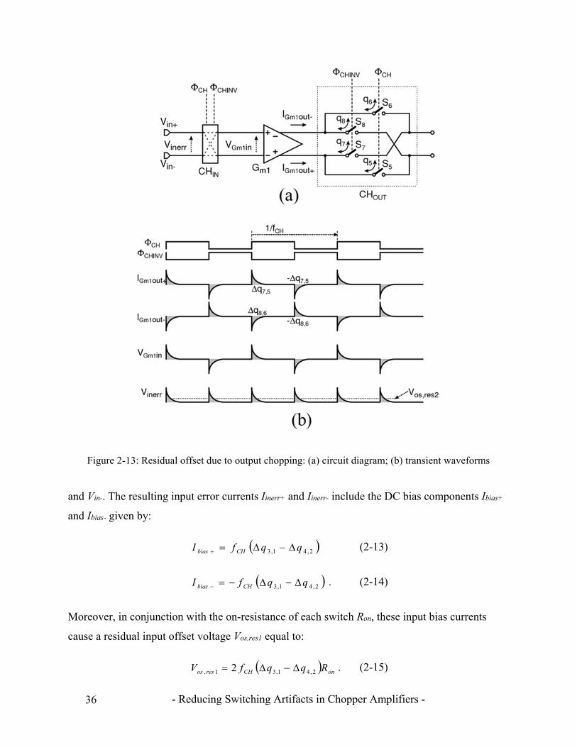
Figure 2-13: Residual offset due to output chopping: (a) circuit diagram; (b) transient waveforms

- Reducing Switching Artifacts in Chopper Amplifiers - 37
Additionally, source resistances driving the input pins should be added in series with Ron in the
equation above, which will further increase Vos,res1. For instance, with fCH = 100kHz and Ron =
1kΩ, a charge injection mismatch Δq3,1 – Δq4,2 = 10fF will result in Ibias+ = 1nA, Ibias– = –1nA,
and Vos,res1 = 2µV. Furthermore, when each input pin is driven by a 10kΩ source resistance,
Vos,res1 increases to 22µV.
The charge injection mismatch of the output chopper CHOUT also causes residual offset.
As shown in Figure 2-13 (a), CHOUT consists of four switches S5-8, which inject charges q5-8. The
charge injection mismatches Δq7,5 = q7 – q5 and Δq8,6 = q8 – q6 result in current glitches IGm1out+
and IGm1out-, respectively, as shown in Figure 2-13 (b). The input transconductor Gm1 absorbs
these current glitches, resulting in voltage glitches VGm1in at its input. The input chopper CHIN
then down-modulates VGm1in, so that the resulting input error voltage Vinerr includes a residual DC
offset Vos,res2 equal to:
1
8,76,52,
2
m
CHresos G
qqfV
. (2-16)
As indicated in the equations, these DC errors are proportional to the chopping frequency fCH.
Furthermore, they indicate that wider switches, which suffer from larger charge injection
mismatch, cause larger DC errors.
- Reducing Switching Artifacts in Chopper Amplifiers - 38
2.4.4 Dynamic Switching Conductance
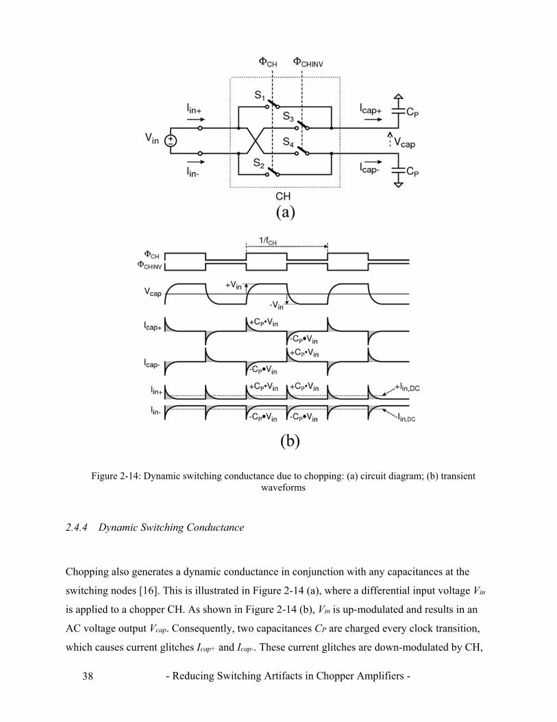
Chopping also generates a dynamic conductance in conjunction with any capacitances at the
switching nodes [16]. This is illustrated in Figure 2-14 (a), where a differential input voltage Vin
is applied to a chopper CH. As shown in Figure 2-14 (b), Vin is up-modulated and results in an
AC voltage output Vcap. Consequently, two capacitances CP are charged every clock transition,
which causes current glitches Icap+ and Icap-. These current glitches are down-modulated by CH,
Figure 2-14: Dynamic switching conductance due to chopping: (a) circuit diagram; (b) transient waveforms
- Reducing Switching Artifacts in Chopper Amplifiers - 39
and become input currents Iin+ and Iin-, including DC component Iin,DC. The dynamic switching
conductance Gswitch is defined as:
PCHin
inDCswitch Cf
V
IG 2, . (2-17)
Because of this effect, a chopper amplifier has a finite differential input conductance. However,
this is usually not a problem for an op-amp amplifying DC or low frequency signals, since the
differential input voltage is kept small by feedback. However, an instrumentation amplifier can
have a large differential input voltage, and so should have a sufficiently low differential input
conductance.
Additionally, the DC gain of the input transconductor Gm1 decreases due to the switching
conductance associated with the output chopper. This not only reduces the open-loop gain of the
op-amp, but it also increases the residual offset contributed by a subsequent gain stage. For
instance, with an 80dB gain of Gm1, a subsequent gain stage with an input offset of 10mV will
give rise to a 1µV residual input offset.
2.4.5 Summary of the Errors
As discussed earlier in this section, the switching artifacts due to chopping cause various DC and
AC errors. The up-modulated ripple and the glitches caused by charge injection show up as noise
spectra peak at the harmonics of the chopping frequency fCH. Moreover, down-modulated charge
injection mismatch causes DC errors such as residual offset and input bias currents.
Design parameters, such as the chopping frequency fCH and the size of the switches,
affect these AC and DC errors, and therefore should be properly chosen for a given design target.
To sufficiently reduce the 1/f noise, fCH should be set above its corner frequency. For applications
requiring a wider signal bandwidth, fCH should be further increased to relax the requirements of
the low-pass filters. However, this increases the residual offset and input bias current, and
decreases the effective DC gain of the input transconductor. Moreover, the variation of fCH over
temperature causes residual offset drift.

- Reducing Switching Artifacts in Chopper Amplifiers - 40
Figure 2-15: Maximum offset versus chopping frequency of previous chopper op-amps
Figure 2-16: Maximum input bias current versus chopping frequency of previous chopper op-amps
- Reducing Switching Artifacts in Chopper Amplifiers - 41
The input switches must be made sufficiently wide to reduce the on-resistance for a
targeted thermal noise PSD. However, this also increases their charge injection mismatch, and
thus increases the residual offset and input bias current. When the chopping clocks have a fixed
amplitude, the amount of charge injection changes with the input common-mode voltage.
Consequently, the residual offset and input bias current also change with the input common-
mode voltage, which degrades the CMRR and the common-mode input impedance. Moreover,
wider switches produce larger glitches and hence larger noise spectra peak.
In summary, chopper op-amp design involves trade-offs between the DC error, the
chopping frequency, and the noise PSD. Figure 2-15 shows the maximum offset versus the
chopping frequency of previous chopper op-amps that have less than 20nV/√Hz noise PSD [17-
27]. Note that the specifications derived from conferences or journals are marked by crosses,
while those derived from the datasheets of commercial products are marked by squares. It can be
seen that their offset tends to increase with chopping frequency, and is typically greater than
10µV for chopping frequencies above 100kHz. Figure 2-16 shows the maximum input bias
current versus the chopping frequency. Like offset, input bias current tends to increase with
chopping frequency, and is higher than 500pA for chopping frequencies above 200kHz.
- Reducing Switching Artifacts in Chopper Amplifiers - 42
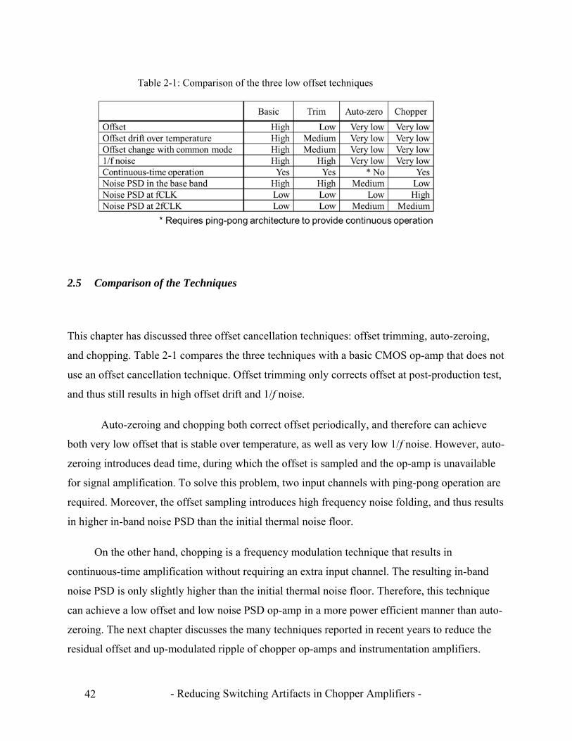
2.5 Comparison of the Techniques
This chapter has discussed three offset cancellation techniques: offset trimming, auto-zeroing,
and chopping. Table 2-1 compares the three techniques with a basic CMOS op-amp that does not
use an offset cancellation technique. Offset trimming only corrects offset at post-production test,
and thus still results in high offset drift and 1/f noise.
Auto-zeroing and chopping both correct offset periodically, and therefore can achieve
both very low offset that is stable over temperature, as well as very low 1/f noise. However, auto-
zeroing introduces dead time, during which the offset is sampled and the op-amp is unavailable
for signal amplification. To solve this problem, two input channels with ping-pong operation are
required. Moreover, the offset sampling introduces high frequency noise folding, and thus results
in higher in-band noise PSD than the initial thermal noise floor.
On the other hand, chopping is a frequency modulation technique that results in
continuous-time amplification without requiring an extra input channel. The resulting in-band
noise PSD is only slightly higher than the initial thermal noise floor. Therefore, this technique
can achieve a low offset and low noise PSD op-amp in a more power efficient manner than auto-
zeroing. The next chapter discusses the many techniques reported in recent years to reduce the
residual offset and up-modulated ripple of chopper op-amps and instrumentation amplifiers.
Table 2-1: Comparison of the three low offset techniques

- Reducing Switching Artifacts in Chopper Amplifiers - 43
2.6 References
[1] J. H. Atherton and H. T. Simmonds, “An Offset Reduction Technique for Use with CMOS
Integrated Comparators and Amplifiers”, IEEE J. Solid-State Circuits, vol. 27, no. 8, pp. 1168-
1175, Aug. 1992.
[2] Analog Devices, “MT-037 Tutorial, Op Amp Input Offset Voltage”, Accessed on March
2018, [Online] Available: <http://www.analog.com/media/en/training-seminars/tutorials/MT-
037.pdf>.
[3] M. Bolatkale, M. A. P. Pertijs, W. J. Kindt, J. H. Huijsing, and K. A. A. Makinwa, “A
Single-Temperature Trimming Technique for MOS-Input Operational Amplifiers Achieving
0.33 µV/°C Offset Drift”, IEEE J. Solid-State Circuits, vol. 46, no. 9, pp. 2099-2017, Sept. 2011.
[4] Analog Devices, “ADA4661-2 Datasheet”, July 2013, Accessed on March 2018, [Online]
Available: <http://www.analog.com/media/en/technical-documentation/data-sheets/ADA4661-
2.pdf>.
[5] Texas Instruments, “OPA192 Data Sheet”, Dec. 2013, Accessed on March 2018, [Online]
Available: <http://www.ti.com/lit/ds/symlink/opa192.pdf>.
[6] Analog Devices, “ADA4077 Datasheet”, Oct. 2012, Accessed on March 2018, [Online]
Available: <http://www.analog.com/media/en/technical-documentation/data-sheets/ADA4077-
1_4077-2_4077-4.pdf>.
[7] B. Razavi, Design of Analog CMOS Integrated Circuits, McGraw Hill, 2001.
[8] C. C. Enz and G. C. Temes, “Circuit Techniques for Reducing the Effect of Op-Amp
Imperfections: Autozeroing, Correlated Double Sampling, and Chopper Stabilization”, Proc. of
IEEE, vol. 84, no. 9, pp. 1320-1324, Sept. 1996.
[9] R. Wu, J. H. Huijsing, and K. A. A. Makinwa, Precision Instrumentation Amplifiers and
Read-Out Integrated Circuits, Springer, New York, 2013.
- Reducing Switching Artifacts in Chopper Amplifiers - 44
[10] M. Pertijs and W. J. Kindt, “A 140 dB-CMRR current-feedback instrumentation amplifier
employing ping-pong auto-zeroing and chopping”, IEEE J. Solid-State Circuits, vol. 45, no. 10,
pp. 2044-2056, Oct. 2010.
[11] I. E. Opris and G. T. A. Kavacs, “A Rail-to-Rail Ping-Pong Op-Amp”, IEEE J. Solid-State
Circuits, vol. 31, no. 9, pp. 1320-1324, Sept. 1996.
[12] J. F. Witte, K. A. A. Makinwa, and J. H. Huijsing, Dynamic Offset Compensated CMOS
Amplifiers, Springer, New York, 2010.
[13] J. Caldwell, “Intrinsic Noise Sources in Chopper Amplifiers”, Accessed on March 2018,
[Online] Available: <http://e2e.ti.com/cfs-file.ashx/__key/telligent-evolution-components-
attachments/00-14-01-00-00-70-21-03/Chopper-Noise.pdf>.
[14] STMicroelectronics, “Input bias current of a chopper amplifier”, Oct. 2014, Accessed on
March 2018, [Online] Available: <http://www.st.com/st-web-
ui/static/active/en/resource/technical/document/application_note/DM00133793.pdf>
[15] V. Wong and Y. Kusuda, “Zero-Drift Amplifiers: Now Easy to Use in High Precision
Circuits”, July 2015, Accessed on March 2018, [Online] Available:
<http://www.analog.com/library/analogdialogue/archives/49-07/Zero-Drift_Amplifiers.pdf>.
[16] Q. Fan, J. Huijsing, and K. Makinwa, “Input Characteristics of a Chopped Multi-Path
Current Feedback Instrumentation Amplifier”, in Proc, 4th Int. Workshop on Advances in Sensors
and Interfaces, IWASI, pp. 61-66, June 2011.
[17] A. T. K. Tang, “A 3V-Offset Operational Amplifier with 20nV/√Hz Input Noise PSD at
DC Employing both Chopping and Autozeroing”, IEEE ISSCC Dig. Tech. Papers, pp. 362-387,
Feb. 2002.
[18] M. Kejariwal, P. Ammisetti, and A. Thomsen, “A 250+dB open loop gain feedforward
compensated high precision operational amplifier”, Proc. of IEEE ESSCIRC, pp. 187-190, Sept.
2002.
- Reducing Switching Artifacts in Chopper Amplifiers - 45
[19] J. F. Witte, K. A. A. Makinwa, and J. H. Huijsing, “A CMOS Chopper Offset-Stabilized
Opamp”, IEEE J. Solid-State Circuits, vol. 42, no. 7, pp. 1529-1535, July 2007.
[20] Q. Fan, J. H. Huijsing, and K.A.A. Makinwa, “A 21 nV/√Hz Chopper-Stabilized Multi-Path
Current-Feedback Instrumentation Amplifier With 2 µV Offset”, IEEE J. Solid-State Circuits,
vol. 47, no. 2, pp. 464-475, Feb. 2012.
[21] Texas Instruments, “OPA378 Datasheet”, Mar. 2006, Accessed on March 2018, [Online]
Available: <http://www.ti.com/lit/gpn/opa378>.
[22] Texas Instruments, “LMP2021 Datasheet”, Sept. 2009, Accessed on March 2018, [Online]
Available: <http://www.ti.com/lit/ds/symlink/lmp2022.pdf>.
[23] Intersil Corporation, “ISL28134 Datasheet”, June 2011, Accessed on March 2018, [Online]
Available: <http://www.intersil.com/content/dam/Intersil/documents/isl2/isl28134.pdf>.
[24] Maxim Integrated, “MAX44250 Datasheet”, Oct. 2011, Accessed on March 2018, [Online]
Available: <http://datasheets.maximintegrated.com/en/ds/MAX44250-MAX44252.pdf>.
[25] Texas Instruments, “OPA2188 Data Sheet”, Aug. 2011, Accessed on March 2018, [Online]
Available: <http://www.ti.com/lit/ds/symlink/opa2188.pdf>.
[26] Maxim Integrated, “MAX44246 Data Sheet”, July 2012, Accessed on March 2018, [Online]
Available: <http://datasheets.maximintegrated.com/en/ds/MAX44241-MAX44246.pdf>.
[27] Analog Devices, “LTC2057HV Data Sheet”, Aug. 2013, Accessed on March 2018, [Online]
Available: <http://www.analog.com/media/en/technical-documentation/data-sheets/2057f.pdf>.

- Reducing Switching Artifacts in Chopper Amplifiers - 46

- Reducing Switching Artifacts in Chopper Amplifiers - 47
Chapter 3
Methods of Reducing Chopper Switching Artifacts
The previous chapter discussed the various DC and AC errors caused by switching artifacts in
chopper amplifiers. This chapter reviews the literature and presents various techniques to reduce
these errors.
- Reducing Switching Artifacts in Chopper Amplifiers - 48
3.1 Residual Offset Reduction Techniques
As explained in Section 2.4.3, the input and output choppers of a chopper amplifier cause voltage
and current glitches due to charge injection mismatch. These glitches can therefore be down-
modulated, producing residual offset and input bias current. This section discusses three known
techniques to reduce these DC errors. The first two techniques attenuate the glitches that would
otherwise be down-modulated to DC. The third technique employs a combination of fast and
slow chopping, in such a way that the slow chopping up-modulates the DC errors produced by
the fast chopping.
3.1.1 Filtering the Glitches
According to the explanation in Section 2.4.3, the charge injection mismatch of CHIN may cause
a residual input offset Vos,res1 in conjunction with the on-resistance of the switches. In fact, the
charge injection mismatch first causes voltage glitches at the input of input transconductor Gm1.
These glitches are then amplified by Gm1 and down-modulated by CHOUT to become residual
offset. Therefore, residual offset can be reduced by attenuating the glitches before they are down-
modulated.
In 1997, Menolfi proposed a band-pass filtering technique to attenuate the glitches [1,2].
A block diagram of the proposed instrumentation amplifier (IA) is shown in Figure 3-1 [2]. The
input signal Vin is up-modulated to a chopping frequency fCH and is amplified by a pre-amplifier
A1. Consequently, the output of A1 (VA1,out) contains glitches caused by an input chopper CHIN
along with the up-modulated signal. A band-pass filter (BPF) attenuates most of the energy in the
wideband glitches that would otherwise become residual offset. The center frequency fBPF of the
BPF is tuned at fCH, so that the up-modulated signal can pass through it. With fCH = fBPF = 6kHz,
the proposed IA achieved a 600nV offset (mean + 1σ), a 150dB CMRR, and an 8.5nV/√Hz noise
PSD. Although the BPF required a relatively relaxed quality factor of Q = 5, 0.5% matching was
required between fBPF and fCH [2]. To meet these requirements, the oscillator and the BPF employ
identical active integrators, which consume extra current and die area.
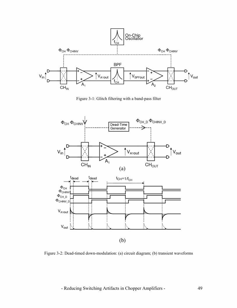
- Reducing Switching Artifacts in Chopper Amplifiers - 49
Figure 3-1: Glitch filtering with a band-pass filter
Figure 3-2: Dead-timed down-modulation: (a) circuit diagram; (b) transient waveforms
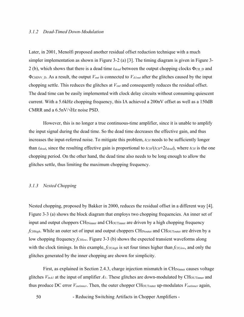
- Reducing Switching Artifacts in Chopper Amplifiers - 50
3.1.2 Dead-Timed Down-Modulation
Later, in 2001, Menolfi proposed another residual offset reduction technique with a much
simpler implementation as shown in Figure 3-2 (a) [3]. The timing diagram is given in Figure 3-
2 (b), which shows that there is a dead time tdead between the output chopping clocks ΦCH_D and
ΦCHINV_D. As a result, the output Vout is connected to VA1out after the glitches caused by the input
chopping settle. This reduces the glitches at Vout and consequently reduces the residual offset.
The dead time can be easily implemented with clock delay circuits without consuming quiescent
current. With a 5.6kHz chopping frequency, this IA achieved a 200nV offset as well as a 150dB
CMRR and a 6.5nV/√Hz noise PSD.
However, this is no longer a true continuous-time amplifier, since it is unable to amplify
the input signal during the dead time. So the dead time decreases the effective gain, and thus
increases the input-referred noise. To mitigate this problem, tCH needs to be sufficiently longer
than tdead, since the resulting effective gain is proportional to tCH/(tCH+2tdead), where tCH is the one
chopping period. On the other hand, the dead time also needs to be long enough to allow the
glitches settle, thus limiting the maximum chopping frequency.
3.1.3 Nested Chopping
Nested chopping, proposed by Bakker in 2000, reduces the residual offset in a different way [4].
Figure 3-3 (a) shows the block diagram that employs two chopping frequencies. An inner set of
input and output choppers CHINinner and CHOUTinner are driven by a high chopping frequency
fCHhigh. While an outer set of input and output choppers CHINouter and CHOUTouter are driven by a
low chopping frequency fCHlow. Figure 3-3 (b) shows the expected transient waveforms along
with the clock timings. In this example, fCH,high is set four times higher than fCH,low, and only the
glitches generated by the inner chopping are shown for simplicity.
First, as explained in Section 2.4.3, charge injection mismatch in CHINinner causes voltage
glitches VinA1 at the input of amplifier A1. These glitches are down-modulated by CHOUTinner and
thus produce DC error Voutinner. Then, the outer chopper CHOUTouter up-modulates Voutinner again,
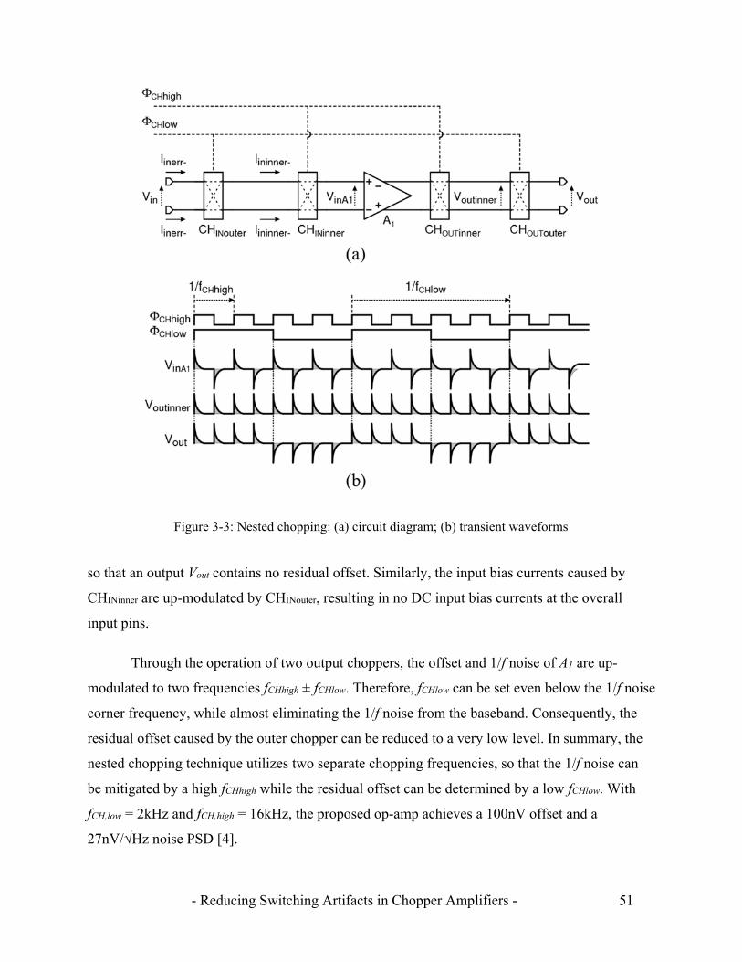
- Reducing Switching Artifacts in Chopper Amplifiers - 51
so that an output Vout contains no residual offset. Similarly, the input bias currents caused by
CHINinner are up-modulated by CHINouter, resulting in no DC input bias currents at the overall
input pins.
Through the operation of two output choppers, the offset and 1/f noise of A1 are up-
modulated to two frequencies fCHhigh ± fCHlow. Therefore, fCHlow can be set even below the 1/f noise
corner frequency, while almost eliminating the 1/f noise from the baseband. Consequently, the
residual offset caused by the outer chopper can be reduced to a very low level. In summary, the
nested chopping technique utilizes two separate chopping frequencies, so that the 1/f noise can
be mitigated by a high fCHhigh while the residual offset can be determined by a low fCHlow. With
fCH,low = 2kHz and fCH,high = 16kHz, the proposed op-amp achieves a 100nV offset and a
27nV/√Hz noise PSD [4].
Figure 3-3: Nested chopping: (a) circuit diagram; (b) transient waveforms
- Reducing Switching Artifacts in Chopper Amplifiers - 52
In 2005, van der Meer reported a Hall sensor read-out IC employing nested chopping,
where the output outer chopper is implemented in the ADC [5]. With fCH,low = 10Hz and fCH,high =
12.5kHz, it achieved a 20nV/√Hz noise PSD and less than 50nV offset.
However, the outer chopper creates spectral peaks at fCHlow and its harmonics, which
limits the usable signal bandwidth. Another drawback is that to achieve a targeted noise PSD,
wider switches must be used, since the switches used for low frequency chopping are in series
with those used for high frequency chopping. The two sets of switches cannot be merged because
a separate set of switches is needed to up-modulate the glitches generated by the inner choppers.
3.2 Ripple Reduction Techniques
This section discusses seven techniques to reduce up-modulated ripple. The first three involve
filtering, while the following four operate by reducing the initial offset that would otherwise
become up-modulated ripple.
3.2.1 Multi-Path Chopper Offset Stabilization
As suggested by Equation (2-11), the up-modulated ripple of a two-stage amplifier can be
attenuated by increasing the size of the frequency compensation capacitors. However, this
method increases the die size, and decreases the signal bandwidth of the op-amp. The ripple can
be attenuated in a more area-efficient manner by a higher order low-pass filter. Additionally, the
cutoff frequency of the low-pass filter can be set separately from the signal bandwidth by
employing a multi-path op-amp architecture. These ideas were proposed by Witte in 2006 [6],
the simplified op-amp block diagram of which is shown in Figure 3-4. This multi-path op-amp
consists of a low frequency path (LFP) and a high frequency path (HFP) in parallel. The LFP
further consists of the input transconductor Gm1 and the subsequent three transconductors Gm2-4,
whereas the HFP consists of the other input transconductor Gm5 and shares Gm4 with the LFP.
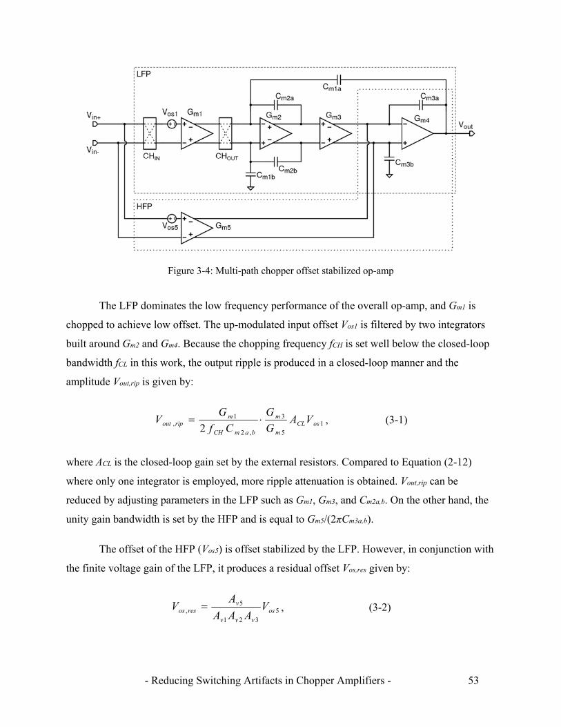
- Reducing Switching Artifacts in Chopper Amplifiers - 53
The LFP dominates the low frequency performance of the overall op-amp, and Gm1 is
chopped to achieve low offset. The up-modulated input offset Vos1 is filtered by two integrators
built around Gm2 and Gm4. Because the chopping frequency fCH is set well below the closed-loop
bandwidth fCL in this work, the output ripple is produced in a closed-loop manner and the
amplitude Vout,rip is given by:
15
3
,2
1, 2 osCL
m
m
bamCH
mripout VA
G
G
Cf
GV , (3-1)
where ACL is the closed-loop gain set by the external resistors. Compared to Equation (2-12)
where only one integrator is employed, more ripple attenuation is obtained. Vout,rip can be
reduced by adjusting parameters in the LFP such as Gm1, Gm3, and Cm2a,b. On the other hand, the
unity gain bandwidth is set by the HFP and is equal to Gm5/(2πCm3a,b).
The offset of the HFP (Vos5) is offset stabilized by the LFP. However, in conjunction with
the finite voltage gain of the LFP, it produces a residual offset Vos,res given by:
5321
5, os
vvv
vresos V
AAA
AV , (3-2)
Figure 3-4: Multi-path chopper offset stabilized op-amp
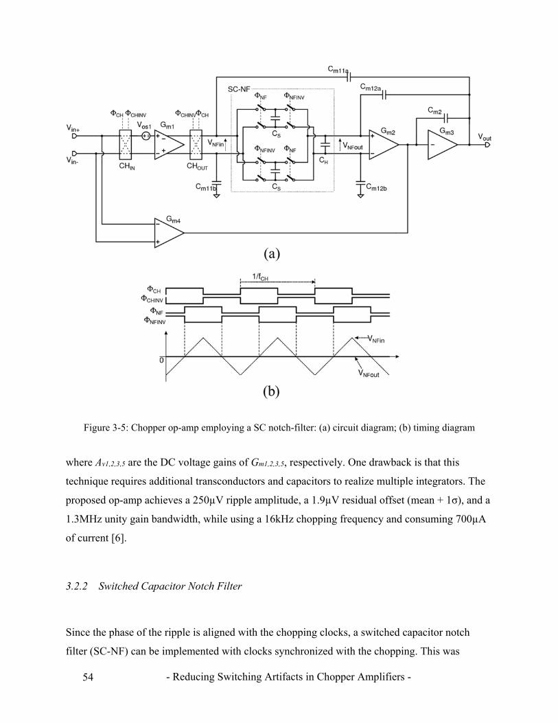
- Reducing Switching Artifacts in Chopper Amplifiers - 54
where Av1,2,3,5 are the DC voltage gains of Gm1,2,3,5, respectively. One drawback is that this
technique requires additional transconductors and capacitors to realize multiple integrators. The
proposed op-amp achieves a 250µV ripple amplitude, a 1.9µV residual offset (mean + 1σ), and a
1.3MHz unity gain bandwidth, while using a 16kHz chopping frequency and consuming 700µA
of current [6].
3.2.2 Switched Capacitor Notch Filter
Since the phase of the ripple is aligned with the chopping clocks, a switched capacitor notch
filter (SC-NF) can be implemented with clocks synchronized with the chopping. This was
Figure 3-5: Chopper op-amp employing a SC notch-filter: (a) circuit diagram; (b) timing diagram
- Reducing Switching Artifacts in Chopper Amplifiers - 55
proposed by Bakker in 1997 [7] and again by Burt in 2006 [8].
Figure 3-5 (a) shows a block diagram of the op-amp proposed in [8]. This again consists
of a LFP and a HFP, where the LFP includes a SC-NF following the chopped input
transconductor Gm1. Figure 3-5 (b) shows the timing diagram of the chopping (ΦCH and ΦCHINV)
and the SC-NF (ΦNF and ΦNFINV), as well as the input and output voltages of the SC-NF (VNFin
and VNFout). First, VNFin contains a triangular ripple due to the up-modulated output current of
Gm1. However, since ΦNF and ΦNFINV operate at the same frequency as ΦCH and ΦCHINV but with
a 90-degree phase difference, the SC-NF samples the triangular ripple whenever the amplitude
becomes zero, and thus results in the ripple free output voltage VNFout. This SC-NF adds a 90-
degree phase delay to the signal at the chopping frequency, so that the HFP is required to bypass
this phase delay and to stabilize the overall op-amp.
This filter does not consume quiescent current, and thus is more power efficient than
active filters. The proposed op-amp consumes 17µA of current and achieves an NEF of 8.7 [8].
However, there are some drawbacks. First, clock skew and sampling capacitor mismatch result in
residual ripple. Second, Gm1 must have a wide output range to tolerate the maximum ripple
amplitude, since the ripple still exists there. This problem becomes more severe in low noise
designs, where the ripple amplitude is proportional to Gm1, as suggested by Equation (2-11).
Third, due to the phase delay introduced by the SC-NF, the LFP requires a complicated
frequency compensation with split Miller capacitors Cm11a and Cm12a. Consequently, the ripple
can couple to the output through Cm11a. Fourth, the sampling action of the SC-NF generates kT/C
noise that contributes to the in-band noise PSD.
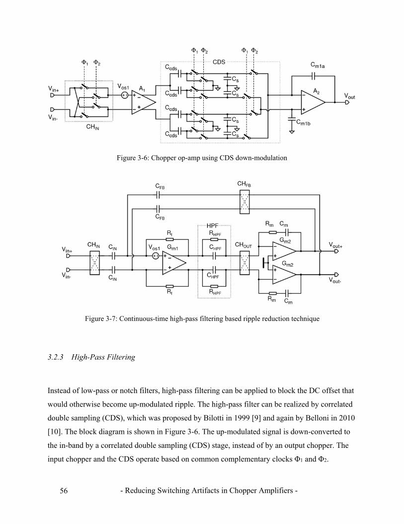
- Reducing Switching Artifacts in Chopper Amplifiers - 56
3.2.3 High-Pass Filtering
Instead of low-pass or notch filters, high-pass filtering can be applied to block the DC offset that
would otherwise become up-modulated ripple. The high-pass filter can be realized by correlated
double sampling (CDS), which was proposed by Bilotti in 1999 [9] and again by Belloni in 2010
[10]. The block diagram is shown in Figure 3-6. The up-modulated signal is down-converted to
the in-band by a correlated double sampling (CDS) stage, instead of by an output chopper. The
input chopper and the CDS operate based on common complementary clocks Φ1 and Φ2.
Figure 3-6: Chopper op-amp using CDS down-modulation
Figure 3-7: Continuous-time high-pass filtering based ripple reduction technique
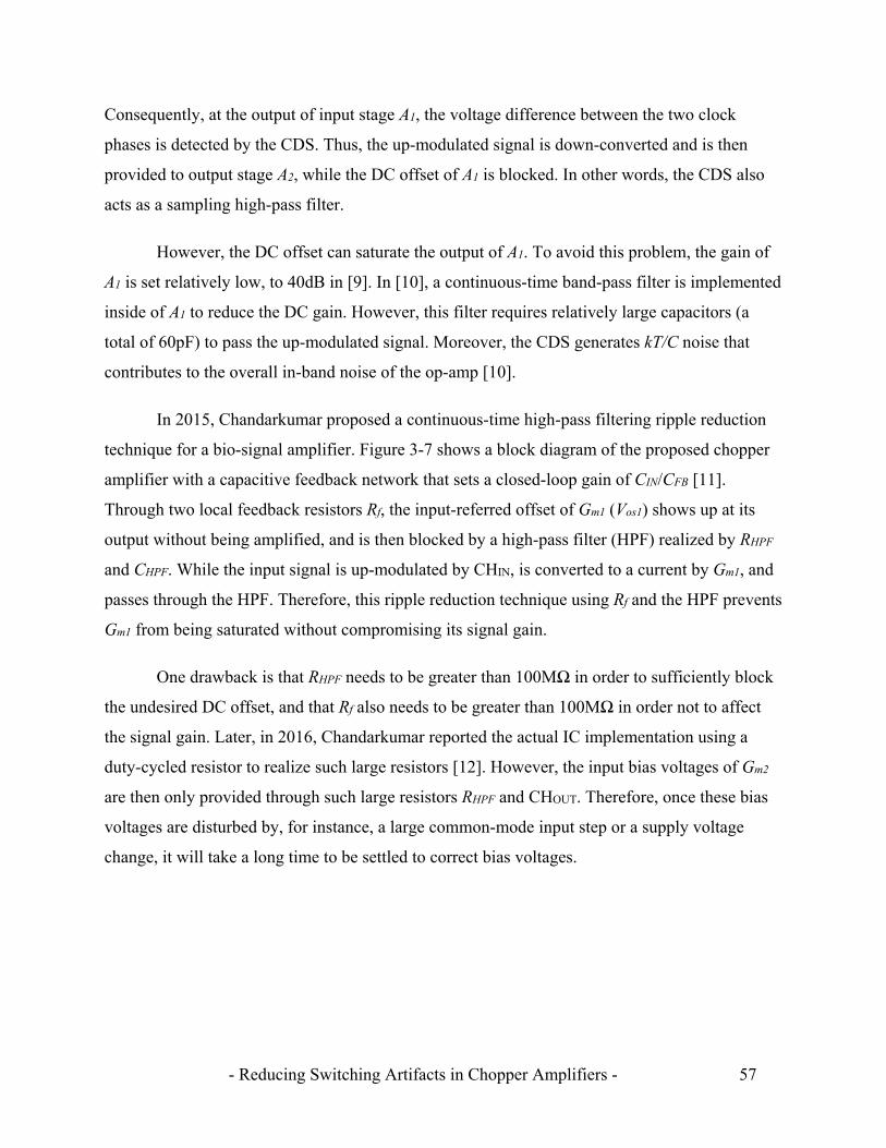
- Reducing Switching Artifacts in Chopper Amplifiers - 57
Consequently, at the output of input stage A1, the voltage difference between the two clock
phases is detected by the CDS. Thus, the up-modulated signal is down-converted and is then
provided to output stage A2, while the DC offset of A1 is blocked. In other words, the CDS also
acts as a sampling high-pass filter.
However, the DC offset can saturate the output of A1. To avoid this problem, the gain of
A1 is set relatively low, to 40dB in [9]. In [10], a continuous-time band-pass filter is implemented
inside of A1 to reduce the DC gain. However, this filter requires relatively large capacitors (a
total of 60pF) to pass the up-modulated signal. Moreover, the CDS generates kT/C noise that
contributes to the overall in-band noise of the op-amp [10].
In 2015, Chandarkumar proposed a continuous-time high-pass filtering ripple reduction
technique for a bio-signal amplifier. Figure 3-7 shows a block diagram of the proposed chopper
amplifier with a capacitive feedback network that sets a closed-loop gain of CIN/CFB [11].
Through two local feedback resistors Rf, the input-referred offset of Gm1 (Vos1) shows up at its
output without being amplified, and is then blocked by a high-pass filter (HPF) realized by RHPF
and CHPF. While the input signal is up-modulated by CHIN, is converted to a current by Gm1, and
passes through the HPF. Therefore, this ripple reduction technique using Rf and the HPF prevents
Gm1 from being saturated without compromising its signal gain.
One drawback is that RHPF needs to be greater than 100MΩ in order to sufficiently block
the undesired DC offset, and that Rf also needs to be greater than 100MΩ in order not to affect
the signal gain. Later, in 2016, Chandarkumar reported the actual IC implementation using a
duty-cycled resistor to realize such large resistors [12]. However, the input bias voltages of Gm2
are then only provided through such large resistors RHPF and CHOUT. Therefore, once these bias
voltages are disturbed by, for instance, a large common-mode input step or a supply voltage
change, it will take a long time to be settled to correct bias voltages.
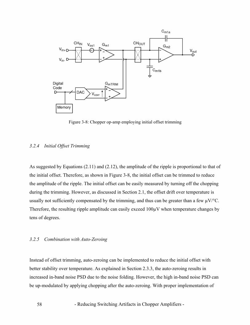
- Reducing Switching Artifacts in Chopper Amplifiers - 58
3.2.4 Initial Offset Trimming
As suggested by Equations (2.11) and (2.12), the amplitude of the ripple is proportional to that of
the initial offset. Therefore, as shown in Figure 3-8, the initial offset can be trimmed to reduce
the amplitude of the ripple. The initial offset can be easily measured by turning off the chopping
during the trimming. However, as discussed in Section 2.1, the offset drift over temperature is
usually not sufficiently compensated by the trimming, and thus can be greater than a few µV/°C.
Therefore, the resulting ripple amplitude can easily exceed 100µV when temperature changes by
tens of degrees.
3.2.5 Combination with Auto-Zeroing
Instead of offset trimming, auto-zeroing can be implemented to reduce the initial offset with
better stability over temperature. As explained in Section 2.3.3, the auto-zeroing results in
increased in-band noise PSD due to the noise folding. However, the high in-band noise PSD can
be up-modulated by applying chopping after the auto-zeroing. With proper implementation of
Figure 3-8: Chopper op-amp employing initial offset trimming
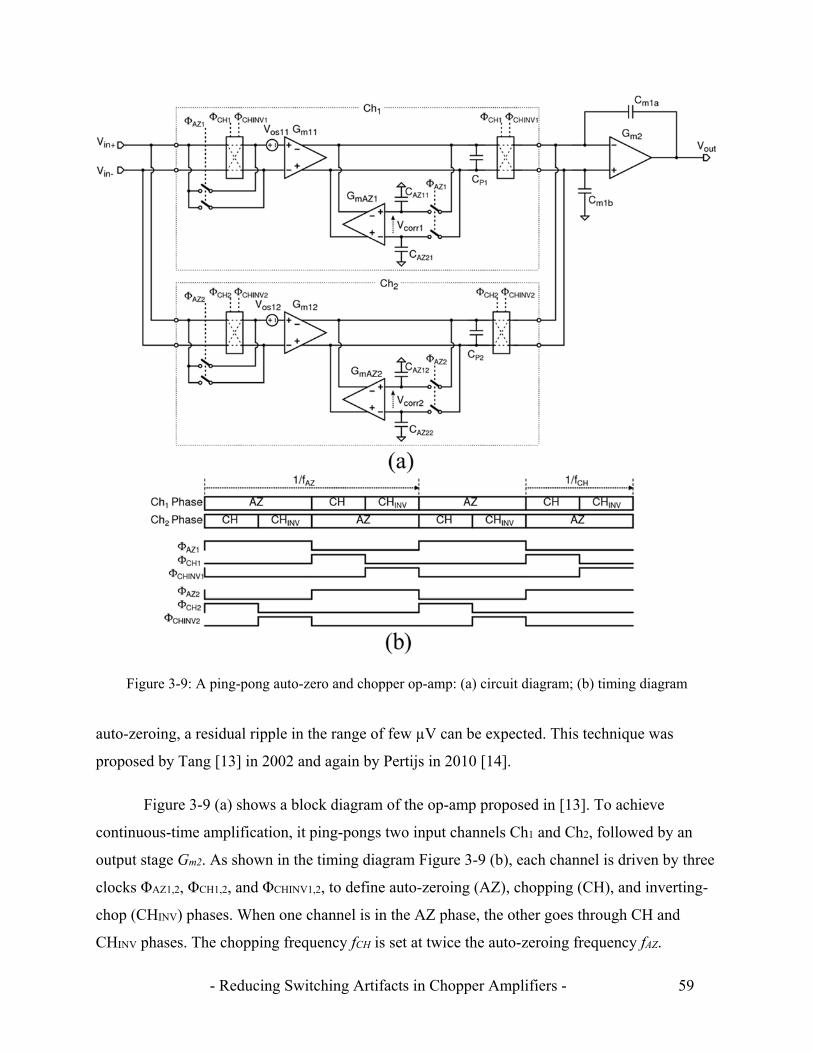
- Reducing Switching Artifacts in Chopper Amplifiers - 59
auto-zeroing, a residual ripple in the range of few µV can be expected. This technique was
proposed by Tang [13] in 2002 and again by Pertijs in 2010 [14].
Figure 3-9 (a) shows a block diagram of the op-amp proposed in [13]. To achieve
continuous-time amplification, it ping-pongs two input channels Ch1 and Ch2, followed by an
output stage Gm2. As shown in the timing diagram Figure 3-9 (b), each channel is driven by three
clocks ΦAZ1,2, ΦCH1,2, and ΦCHINV1,2, to define auto-zeroing (AZ), chopping (CH), and inverting-
chop (CHINV) phases. When one channel is in the AZ phase, the other goes through CH and
CHINV phases. The chopping frequency fCH is set at twice the auto-zeroing frequency fAZ.
Figure 3-9: A ping-pong auto-zero and chopper op-amp: (a) circuit diagram; (b) timing diagram
- Reducing Switching Artifacts in Chopper Amplifiers - 60
In Figure 3-10 (a), (b), and (c), noise PSDs are shown without auto-zeroing or chopping,
after the auto-zeroing, and after the auto-zeroing and the chopping, respectively. The auto-
zeroing almost eliminates 1/f noise, but introduces increased in-band noise PSD. This increased
noise PSD lies in between DC and fAZ, since the offset sampling occurs twice per auto-zeroing
period 1/fAZ. The chopping then up-modulates this high noise PSD up to fCH, to obtain an in-band
noise PSD that is only slightly higher than the initial thermal noise floor. Another way, proposed
in [14], is to set the auto-zeroing loop bandwidth lower than the auto-zeroing frequency fAZ. This
still results in a higher noise PSD at DC, but up to a lower frequency than fAZ. Therefore, the
chopping frequency can be set lower than fAZ without degrading the resulting in-band noise PSD.
The op-amp proposed in [13] achieves a 3µV offset and a 20nV/√Hz in-band noise PSD,
while consuming 800µA of current (NEF = 21.8). One drawback is the additional current
consumption and die area for one extra input channel. Additionally, the ping-pong operation
causes transient glitches, since parasitic capacitances CP1 and CP2 are charged to different
voltages due to the mismatch of the offset correction voltages Vcorr1 and Vcorr2. Moreover, Vcorr1
and Vcorr2 are usually higher than the initial offsets, since GmAZ1,2 is set smaller than Gm11,12 to
reduce the charge injection error as suggested by Equation (2-7).
Figure 3-10: Noise PSDs (a) without auto-zeroing or chopping, (b) after auto-zeroing, and (c) after auto-zeroing and chopping
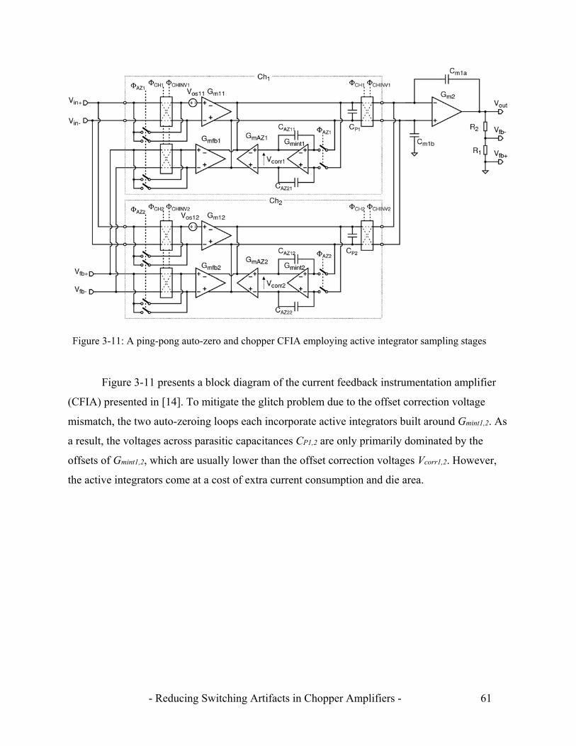
- Reducing Switching Artifacts in Chopper Amplifiers - 61
Figure 3-11 presents a block diagram of the current feedback instrumentation amplifier
(CFIA) presented in [14]. To mitigate the glitch problem due to the offset correction voltage
mismatch, the two auto-zeroing loops each incorporate active integrators built around Gmint1,2. As
a result, the voltages across parasitic capacitances CP1,2 are only primarily dominated by the
offsets of Gmint1,2, which are usually lower than the offset correction voltages Vcorr1,2. However,
the active integrators come at a cost of extra current consumption and die area.
Figure 3-11: A ping-pong auto-zero and chopper CFIA employing active integrator sampling stages
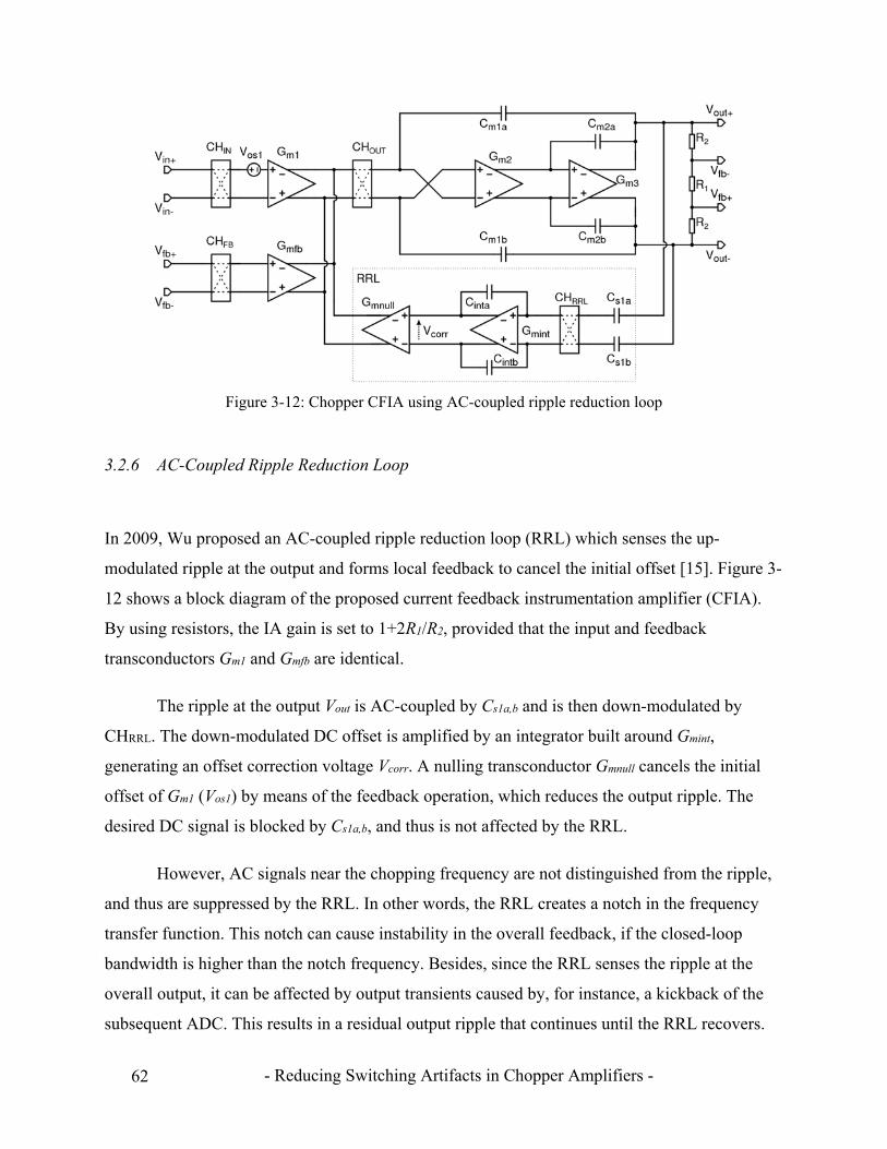
- Reducing Switching Artifacts in Chopper Amplifiers - 62
3.2.6 AC-Coupled Ripple Reduction Loop
In 2009, Wu proposed an AC-coupled ripple reduction loop (RRL) which senses the up-
modulated ripple at the output and forms local feedback to cancel the initial offset [15]. Figure 3-
12 shows a block diagram of the proposed current feedback instrumentation amplifier (CFIA).
By using resistors, the IA gain is set to 1+2R1/R2, provided that the input and feedback
transconductors Gm1 and Gmfb are identical.
The ripple at the output Vout is AC-coupled by Cs1a,b and is then down-modulated by
CHRRL. The down-modulated DC offset is amplified by an integrator built around Gmint,
generating an offset correction voltage Vcorr. A nulling transconductor Gmnull cancels the initial
offset of Gm1 (Vos1) by means of the feedback operation, which reduces the output ripple. The
desired DC signal is blocked by Cs1a,b, and thus is not affected by the RRL.
However, AC signals near the chopping frequency are not distinguished from the ripple,
and thus are suppressed by the RRL. In other words, the RRL creates a notch in the frequency
transfer function. This notch can cause instability in the overall feedback, if the closed-loop
bandwidth is higher than the notch frequency. Besides, since the RRL senses the ripple at the
overall output, it can be affected by output transients caused by, for instance, a kickback of the
subsequent ADC. This results in a residual output ripple that continues until the RRL recovers.
Figure 3-12: Chopper CFIA using AC-coupled ripple reduction loop
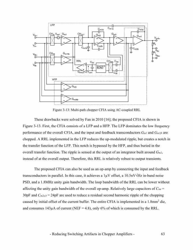
- Reducing Switching Artifacts in Chopper Amplifiers - 63
These drawbacks were solved by Fan in 2010 [16]; the proposed CFIA is shown in
Figure 3-13. First, the CFIA consists of a LFP and a HFP. The LFP dominates the low frequency
performance of the overall CFIA, and the input and feedback transconductors Gm1 and Gm1fb are
chopped. A RRL implemented in the LFP reduces the up-modulated ripple, but creates a notch in
the transfer function of the LFP. This notch is bypassed by the HFP, and thus buried in the
overall transfer function. The ripple is sensed at the output of an integrator built around Gm2,
instead of at the overall output. Therefore, this RRL is relatively robust to output transients.
The proposed CFIA can also be used as an op-amp by connecting the input and feedback
transconductors in parallel. In this case, it achieves a 1µV offset, a 10.5nV√Hz in-band noise
PSD, and a 1.8MHz unity gain bandwidth. The loop bandwidth of the RRL can be lower without
affecting the unity gain bandwidth of the overall op-amp. Relatively large capacitors of Cint =
30pF and Cm2a,b = 24pF are used to reduce a residual second harmonic ripple of the chopping
caused by initial offset of the current buffer. The entire CFIA is implemented in a 1.8mm2 die,
and consumes 143µA of current (NEF = 4.8), only 6% of which is consumed by the RRL.
Figure 3-13: Multi-path chopper CFIA using AC-coupled RRL
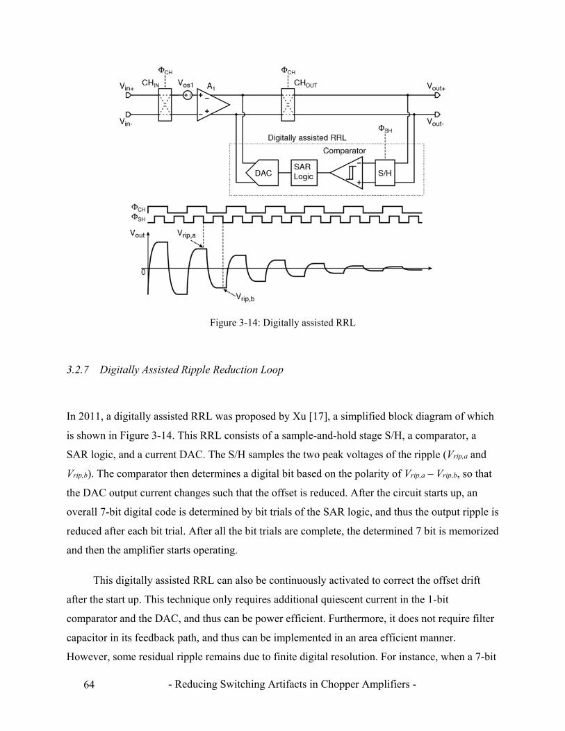
- Reducing Switching Artifacts in Chopper Amplifiers - 64
3.2.7 Digitally Assisted Ripple Reduction Loop
In 2011, a digitally assisted RRL was proposed by Xu [17], a simplified block diagram of which
is shown in Figure 3-14. This RRL consists of a sample-and-hold stage S/H, a comparator, a
SAR logic, and a current DAC. The S/H samples the two peak voltages of the ripple (Vrip,a and
Vrip,b). The comparator then determines a digital bit based on the polarity of Vrip,a – Vrip,b, so that
the DAC output current changes such that the offset is reduced. After the circuit starts up, an
overall 7-bit digital code is determined by bit trials of the SAR logic, and thus the output ripple is
reduced after each bit trial. After all the bit trials are complete, the determined 7 bit is memorized
and then the amplifier starts operating.
This digitally assisted RRL can also be continuously activated to correct the offset drift
after the start up. This technique only requires additional quiescent current in the 1-bit
comparator and the DAC, and thus can be power efficient. Furthermore, it does not require filter
capacitor in its feedback path, and thus can be implemented in an area efficient manner.
However, some residual ripple remains due to finite digital resolution. For instance, when a 7-bit
Figure 3-14: Digitally assisted RRL
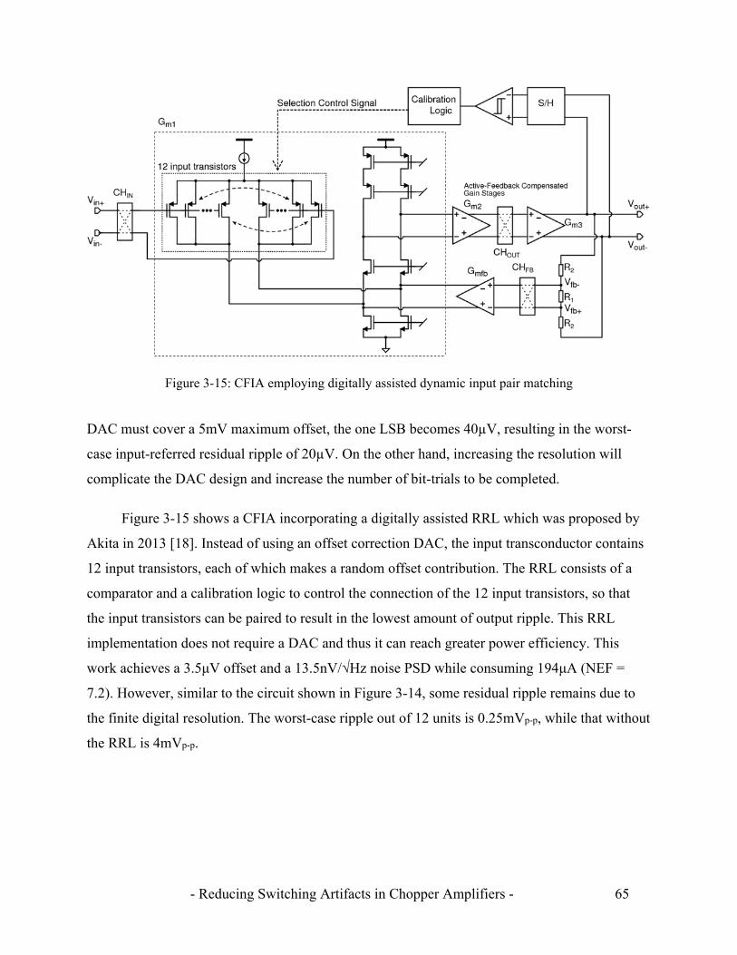
- Reducing Switching Artifacts in Chopper Amplifiers - 65
DAC must cover a 5mV maximum offset, the one LSB becomes 40µV, resulting in the worst-
case input-referred residual ripple of 20µV. On the other hand, increasing the resolution will
complicate the DAC design and increase the number of bit-trials to be completed.
Figure 3-15 shows a CFIA incorporating a digitally assisted RRL which was proposed by
Akita in 2013 [18]. Instead of using an offset correction DAC, the input transconductor contains
12 input transistors, each of which makes a random offset contribution. The RRL consists of a
comparator and a calibration logic to control the connection of the 12 input transistors, so that
the input transistors can be paired to result in the lowest amount of output ripple. This RRL
implementation does not require a DAC and thus it can reach greater power efficiency. This
work achieves a 3.5μV offset and a 13.5nV/√Hz noise PSD while consuming 194μA (NEF =
7.2). However, similar to the circuit shown in Figure 3-14, some residual ripple remains due to
the finite digital resolution. The worst-case ripple out of 12 units is 0.25mVp-p, while that without
the RRL is 4mVp-p.
Figure 3-15: CFIA employing digitally assisted dynamic input pair matching

- Reducing Switching Artifacts in Chopper Amplifiers - 66
3.3 Comparison of the Techniques
This chapter has reviewed various techniques to reduce DC errors such as residual offset and
input bias current. Menolfi proposed a band-pass filtering technique to attenuate the glitches that
would otherwise be down-modulated and turn into residual offset [2]. However, this technique
requires an additional oscillator and a band-pass filter with a matching center frequency. Later,
Menolfi also proposed a dead-timed down-modulation technique that attenuates the glitches
without consuming extra current [3]. However, to mitigate the effective gain reduction, one
chopping period needs to be sufficiently longer than the dead time, which limits the maximum
achievable chopping frequency. By using the nested chopping proposed by Bakker [4], the
residual offset and input bias current, caused by the inner fast chopping, are up-modulated by the
outer slow chopping. However, this generates a high noise spectrum at the slow chopping
frequency, which limits the usable signal bandwidth. Therefore, new circuit techniques should be
explored to reduce DC errors, while offering a high usable signal bandwidth.
This chapter has also reviewed the various ripple reduction techniques. Table 3-1
Table 3-1: Comparison of chopper op-amps employing ripple reduction technique
- Reducing Switching Artifacts in Chopper Amplifiers - 67
compares the performances of the chopper op-amps employing these ripple reduction techniques.
Since some techniques consume more extra current and die area than others, the figures-of-merit,
such as the NEF and GBW/Isy, should be compared in addition to the die area. One way to
reduce the ripple is to filter the up-modulated ripple by active integrators at the cost of extra
current [6]. Instead, a SC notch filter can filter the ripple without consuming extra current [7,8],
although the ripple remains at the output chopper, which limits the design of the input
transconductor. In [9,10], the output chopping is replaced by CDS that down-converts the up-
modulated signal while blocking the DC offset. However, the input amplifier needs to have a
relatively low gain [9] or have a band-pass characteristic [10], in order not to saturate its output
with the DC offset. In [11,12], local feedback resistors are placed around the input
transconductor, in order not to amplify its offset and not to saturate its output. However, these
feedback resistors need to be greater than 100MΩ in order not to affect the signal gain, which
will increase the time required to recover from some disturbances. In these three ripple reduction
techniques, the initial offset remains, which causes problems and/or complicates the design.
Therefore, the preferred approach is to reduce the initial offset that would otherwise turn
into the output ripple. One way to reduce an initial offset is simply with trimming, although the
offset (i.e. the ripple) will increase when temperature changes. Instead, the initial offset can be
auto-zeroed, and then the resulting high noise PSD in the in-band can be up-modulated by the
chopping [13,14]. However, to achieve continuous-time amplification, this requires an additional
input channel that consumes extra current and die area. Another technique is to use a ripple
reduction loop (RRL) that continuously detects the ripple and cancels the initial offset by the
feedback [15]. However, this creates a notch in the signal transfer function, which can cause
instability in the overall feedback loop. This notch can be buried by adding a HFP [16]. The RRL
can be digitally assisted with a comparator, a SAR logic, and a current DAC to cancel the offset
[17]. This technique can be more area efficient without requiring filter capacitor in its feedback
path, although higher digital resolution is required to reduce the residual ripple.
If auto-zeroing is used, then as indicated by Equation (2-7), the initial offset (i.e. the ripple)
can be reduced by a factor equal to the auto-zeroing loop gain, as long as the charge injection
related errors are negligible. Similarly, the ripple can be reduced by a factor equal to the gain of
the RRL. Therefore, these techniques can achieve microvolt-level ripple. This thesis also

- Reducing Switching Artifacts in Chopper Amplifiers - 68
proposes ripple reduction techniques that reduce the initial offset (i.e. the ripple) in a power and
area efficient manner. In the designs discussed in Chapter 4 and 5, ripple is detected and then
suppressed as in a RRL (Figure 3-13), but a switched-capacitor notch filter is employed in the
feedback path instead of a continuous-time filter. In Chapter 6, the initial offset is reduced by
auto-zeroing but in a more power efficient manner than the approach shown in Figure 3-9.
Provided the ripple is sufficiently reduced, the output glitches caused by charge injection can still
result in high noise spectra. Therefore, this thesis also explores new circuit techniques that
address both the ripple and the glitches.

- Reducing Switching Artifacts in Chopper Amplifiers - 69
3.4 References
[1] C. Menolfi and Q. Huang, “A Low-Noise CMOS Instrumentation Amplifier”, IEEE J. Solid-
State Circuits, vol. 32, no. 7, pp. 968-976, July 1997.
[2] C. Menolfi and Q. Huang, “A CMOS instrumentation amplifier with 600 nV offset, 8.5
nV/√Hz noise and 150 dB CMRR”, IEEE CICC Dig. Tech. Papers, pp. 369-372, Sept. 1998.
[3] C. Menolfi and Q. Huang, “A 200nV Offset 6.5nV/√Hz Noise PSD 5.6kHz Chopper
Instrumentation Amplifier in 1µm Digital CMOS”, IEEE ISSCC Dig. Tech. Papers, pp. 362-363,
Feb. 2001.
[4] A. Bakker, K. Thiele, and J. H. Huijsing, “A CMOS Nested-Chopper Instrumentation
Amplifier with 100-nV Offset”, IEEE J. Solid-State Circuits, vol. 35, no. 12, pp. 1877-1883,
Dec. 2000.
[5] J. C. van der Meer, F. R. Riedijk, E. van Kampen, K. A. A. Makinwa, and J. H. Huijsing, “A
fully integrated CMOS Hall sensor with a 3.65µT 3σ offset for compass applications”, IEEE
ISSCC Dig. Tech. Papers, pp. 246-247, Feb. 2005.
[6] J. F. Witte, K. A. A. Makinwa, and J. H. Huijsing, “A CMOS Chopper Offset-Stabilized
Opamp”, IEEE J. Solid-State Circuits, vol. 42, no. 7, pp. 1529-1535, July 2007.
[7] A. Bakker and J.H. Huijsing, “A CMOS Chopper Opamp with Integrated Low-Pass Filter”,
Proc. of IEEE ESSCIRC, pp. 200-203, Sept. 1997.
[8] R. Burt and J. Zhang, “A Micropower Chopper-Stabilized Operational Amplifier using a SC
Notch Filter with Synchronous Integration inside the Continuous-Time Signal Path”, IEEE J.
Solid-State Circuits, vol. 41, no. 12, pp. 2729-2736, Dec. 2006.
[9] A. Bilotti and G. Monreal, “Chopper-Stabilized Amplifiers with a Track-and-Hold Signal
Demodulator”, IEEE Transactions on Circuits and Systems, vol. 46, no. 4, pp. 490-495, Apr.
1999.
- Reducing Switching Artifacts in Chopper Amplifiers - 70
[10] M. Belloni, E. Bonizzoni, A. Fornasari, and F. Maloberti, “A Micropower Chopper-CDS
Operational Amplifier”, IEEE J. Solid-State Circuits, vol. 45, no. 12, pp. 2521-2529, Dec. 2010.
[11] H. Chandrakumar and D. Markovic, “A Simple Area-Efficient Ripple-Rejection Technique
for Chopped Biosignal Amplifiers”, IEEE Transactions on Circuits and Systems—II: Express
Briefs, vol. 62, no. 2, pp. 189-193, Feb. 2015.
[12] H. Chandrakumar and D. Markovic, “A 2µW 40mVpp Linear-Input-Range Chopper-
Stabilized Bio-Signal Amplifier with Boosted Input Impedance of 300MΩ and Electrode-Offset
Filtering”, IEEE ISSCC Dig. Tech. Papers, pp. 96-97, Feb. 2016.
[13] A. T. K. Tang, “A 3V-Offset Operational Amplifier with 20nV/√Hz Input Noise PSD at
DC Employing both Chopping and Autozeroing”, IEEE ISSCC Dig. Tech. Papers, pp. 362-387,
Feb. 2002.
[14] M. Pertijs and W. J. Kindt, “A 140 dB-CMRR current-feedback instrumentation amplifier
employing ping-pong auto-zeroing and chopping”, IEEE J. Solid-State Circuits, vol. 45, no. 10,
pp. 2044-2056, Oct. 2010.
[15] R. Wu, K. A. A. Makinwa, and J. H. Huijsing, “A Chopper Current-Feedback
Instrumentation Amplifier with a 1 mHz 1/f Noise Corner and an AC-Coupled Ripple Reduction
Loop”, IEEE J. Solid-State Circuits, vol. 44, no. 12, pp. 3232-3243, Dec. 2009.
[16] Q. Fan, J. H. Huijsing, and K.A.A. Makinwa, “A 21 nV/√Hz Chopper-Stabilized Multi-Path
Current-Feedback Instrumentation Amplifier With 2 µV Offset”, IEEE J. Solid-State Circuits,
vol. 47, no. 2, pp. 464-475, Feb. 2012.
[17] J. Xu, R. F. Yazicioglu, P. Harpe, K. A. A. Makinwa, and C. V. Hoof, “A 160µW 8-
Channel Active Electrode System for EEG Monitoring”, IEEE ISSCC Dig. Tech. Papers, pp.
300-301, Feb. 2011.
[18] I. Akita and M. Ishida, “A 0.06mm2 14nV/√Hz Chopper Instrumentation Amplifier with
Automatic Differential-Pair Matching”, IEEE ISSCC Dig. Tech. Papers, pp. 178-179, Feb. 2013.

- Reducing Switching Artifacts in Chopper Amplifiers - 71
Chapter 4
Chopper Op-Amp with Auto-Correction Feedback1
This chapter proposes a ripple reduction technique, called auto-correction feedback (ACFB). It
senses the up-modulated ripple in the internal circuit nodes, forms local feedback, and cancels
the initial offset to reduce the output ripple. The proposed ACFB has been implemented in a
stand-alone chopper op-amp which occupies a 0.64mm2 die area in a 0.35m CMOS process
augmented by 5V CMOS transistors. The op-amp only draws 13A from a 1.8V to 5.5V supply,
and operates over a rail-to-rail input common-mode voltage range and a –40°C to 125°C
temperature range. It achieves a 10V maximum offset, a 50pA maximum input bias current, a
95nV/√Hz in-band noise PSD, and a 120kHz unity gain bandwidth. With the use of the ACFB,
the worst-case ripple spectrum is reduced from 4.8mVrms to 42Vrms at the 50kHz chopping
frequency.
First, Section 4.1 describes the motivation for designing a low offset, low power op-amp
for portable applications. Next, Section 4.2 presents the overall chopper op-amp architecture
employing the ACFB, followed by a residual error analysis in Section 4.3. Section 4.4 then
presents transistor-level circuit implementation including the transconductors and the clock
generator. Lastly, Section 4.5 discusses the measurement results, and the chapter ends with a
conclusion in Section 4.6.
______________________
1This chapter is derived from a journal publication of the author: Y. Kusuda, “Auto Correction Feedback for Ripple
Suppression in a Chopper Amplifier”, IEEE J. Solid-State Circuits, vol. 45, no. 8, pp. 1436-1445, Aug. 2010.
- Reducing Switching Artifacts in Chopper Amplifiers - 72
4.1 Motivation
As described in Section 1.5.1, biomedical sensing applications such as EEG, ECG, and EMG,
require precision op-amps that can achieve both low 1/f noise and low input bias current below
100pA [1-3]. Additionally, to serve portable and wearable applications, such op-amps should
also have a current consumption lower than 20µA, a die size smaller than 0.7mm2, and a supply
voltage range including 1.8V. The bandwidth of these biomedical signals is about 200Hz, which
allows the use of an external low-pass filter to reduce ripple, although the op-amp should still
have a relatively small output ripple. For instance, to achieve microvolt-level ripple after 40dB
filter attenuation, the op-amp must have an output ripple amplitude in the order of 100
microvolts. This is much smaller than the ripple associated with the native offset of a CMOS
differential pair, and thus can only be achieved with the aid of an on-chip ripple reduction
technique.
Previous ripple reduction techniques were reviewed in Section 3.2 [4-15]. However, the
techniques in [4,10-12] consume extra current, while those in [5-9] require higher chopping
frequency thus resulting in higher input bias current. The RRL technique in [14] senses and
reduces the ripple by feedback in a power efficient way without requiring higher chopping
frequency. The digitally assisted RRL in [15] can be implemented in a more area efficient
manner without requiring large filter capacitor in its feedback path, although higher digital
resolution is required to reduce the residual ripple.
In order to serve the portable biomedical applications described above, another ripple
reduction technique, called auto-correction feedback (ACFB), is proposed in this chapter. Similar
to the RRL, the ACFB senses and reduces the ripple by feedback with a power efficient manner
as well as an area efficient manner. Moreover, it has a design flexibility to select a relatively low
chopping frequency, thus achieving a relatively low input bias current. On the other hand, the
ripple reduction capability of the ACFB is limited by its relatively small loop gain, although the
remaining output ripple can be attenuated by an external low-pass filter in applications such as
ECG readout which only require low signal bandwidth. Furthermore, it causes a noise PSD peak
around the chopping frequency.
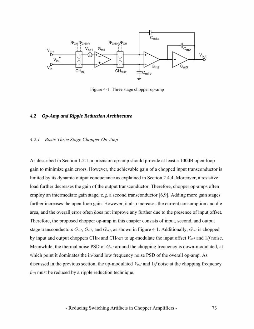
- Reducing Switching Artifacts in Chopper Amplifiers - 73
4.2 Op-Amp and Ripple Reduction Architecture
4.2.1 Basic Three Stage Chopper Op-Amp
As described in Section 1.2.1, a precision op-amp should provide at least a 100dB open-loop
gain to minimize gain errors. However, the achievable gain of a chopped input transconductor is
limited by its dynamic output conductance as explained in Section 2.4.4. Moreover, a resistive
load further decreases the gain of the output transconductor. Therefore, chopper op-amps often
employ an intermediate gain stage, e.g. a second transconductor [6,9]. Adding more gain stages
further increases the open-loop gain. However, it also increases the current consumption and die
area, and the overall error often does not improve any further due to the presence of input offset.
Therefore, the proposed chopper op-amp in this chapter consists of input, second, and output
stage transconductors Gm1, Gm2, and Gm3, as shown in Figure 4-1. Additionally, Gm1 is chopped
by input and output choppers CHIN and CHOUT to up-modulate the input offset Vos1 and 1/f noise.
Meanwhile, the thermal noise PSD of Gm1 around the chopping frequency is down-modulated, at
which point it dominates the in-band low frequency noise PSD of the overall op-amp. As
discussed in the previous section, the up-modulated Vos1 and 1/f noise at the chopping frequency
fCH must be reduced by a ripple reduction technique.
Figure 4-1: Three stage chopper op-amp

- Reducing Switching Artifacts in Chopper Amplifiers - 74
4.2.2 Auto-Correction Feedback
As discussed in Section 2.4.1, the amplitude of the up-modulated ripple can be decreased by
reducing the initial offset Vos1. Figure 4-2 shows a proposed ripple reduction technique, called
auto-correction feedback (ACFB), which is implemented in the three stage chopper op-amp
shown in Figure 4-1. The ACFB consists of a sensing transconductor Gmsense, a chopper CHACFB,
a switched capacitor notch filter SC-NF, and a nulling transconductor Gmnull. First, the up-
modulated ripple is sensed at the Vsense nodes by Gmsense, and is down-modulated by CHACFB,
which operates with the same clock timing as CHIN and CHOUT. The down-modulated DC offset
component passes the SC-NF and generates an offset correction voltage Vcorr, such that Gmnull
cancels Vos1.
In contrast to [14], the ACFB senses the ripple at the Vsense nodes which are at the output
of the output chopper. Clamp diodes D1-4 are added, to maintain the Vsense nodes stable, and
hence the ACFB even in the presence of external output transients. This technique can be applied
to chopper op-amps consisting of two or more gain stages without requiring an extra gain stage
in their main signal path. On the other hand, as will be analyzed in Section 4.3.1, the Vsense nodes
are also at the input of Gm2, which is a virtual ground, thus resulting in a small ripple amplitude
and hence small loop gain of the ACFB.
Figure 4-2: Three stage chopper op-amp employing auto-correction feedback (ACFB)
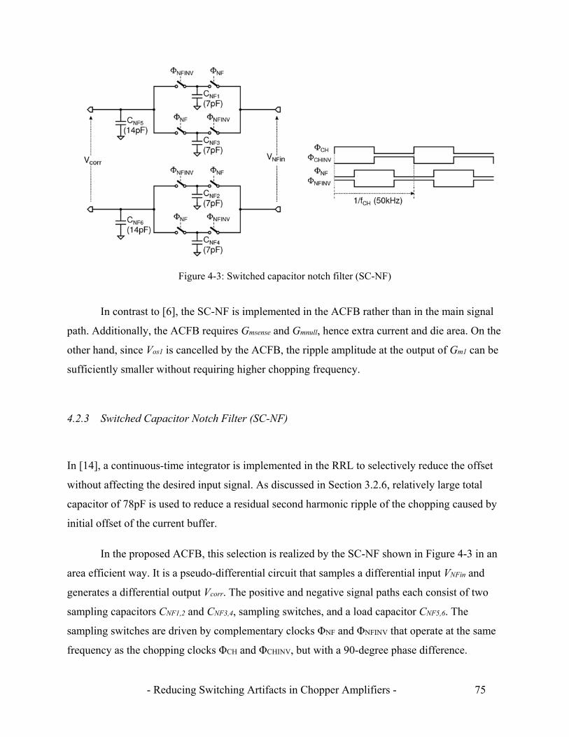
- Reducing Switching Artifacts in Chopper Amplifiers - 75
In contrast to [6], the SC-NF is implemented in the ACFB rather than in the main signal
path. Additionally, the ACFB requires Gmsense and Gmnull, hence extra current and die area. On the
other hand, since Vos1 is cancelled by the ACFB, the ripple amplitude at the output of Gm1 can be
sufficiently smaller without requiring higher chopping frequency.
4.2.3 Switched Capacitor Notch Filter (SC-NF)
In [14], a continuous-time integrator is implemented in the RRL to selectively reduce the offset
without affecting the desired input signal. As discussed in Section 3.2.6, relatively large total
capacitor of 78pF is used to reduce a residual second harmonic ripple of the chopping caused by
initial offset of the current buffer.
In the proposed ACFB, this selection is realized by the SC-NF shown in Figure 4-3 in an
area efficient way. It is a pseudo-differential circuit that samples a differential input VNFin and
generates a differential output Vcorr. The positive and negative signal paths each consist of two
sampling capacitors CNF1,2 and CNF3,4, sampling switches, and a load capacitor CNF5,6. The
sampling switches are driven by complementary clocks ΦNF and ΦNFINV that operate at the same
frequency as the chopping clocks ΦCH and ΦCHINV, but with a 90-degree phase difference.
Figure 4-3: Switched capacitor notch filter (SC-NF)
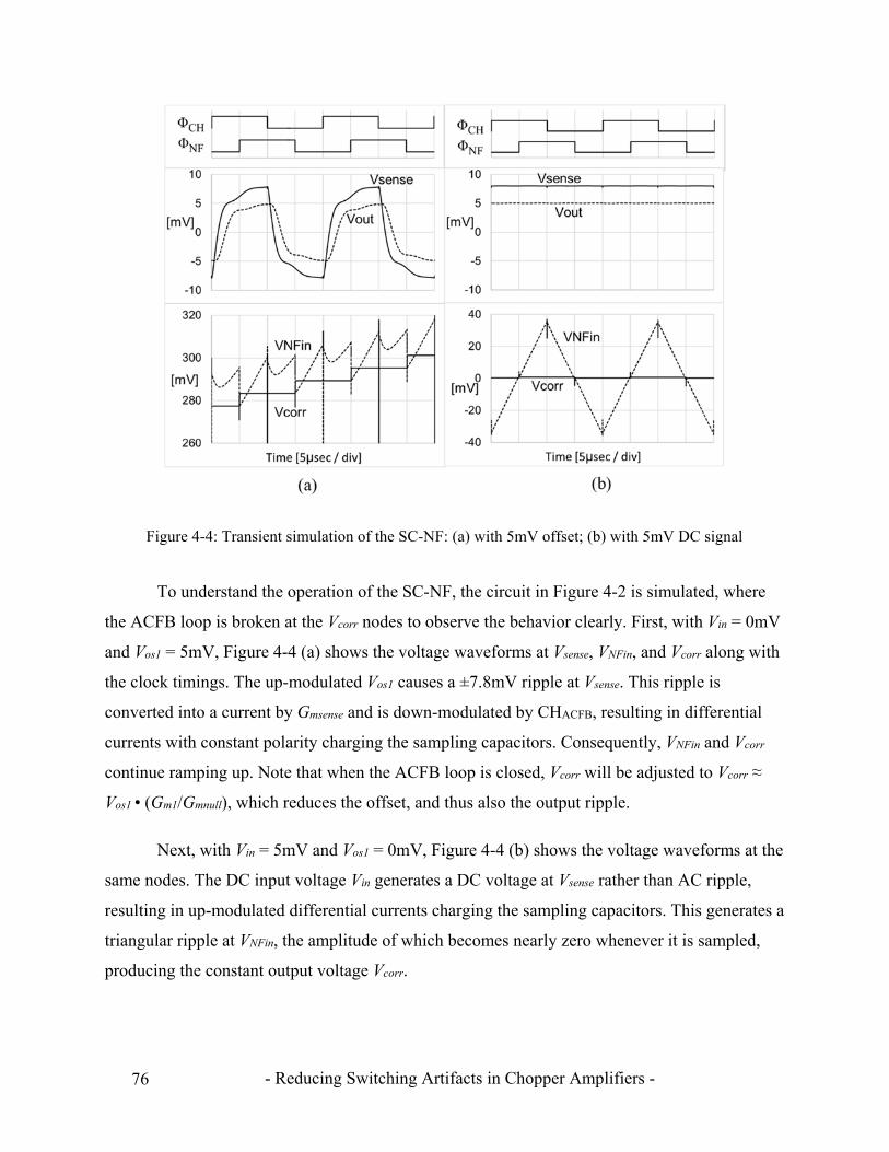
- Reducing Switching Artifacts in Chopper Amplifiers - 76
To understand the operation of the SC-NF, the circuit in Figure 4-2 is simulated, where
the ACFB loop is broken at the Vcorr nodes to observe the behavior clearly. First, with Vin = 0mV
and Vos1 = 5mV, Figure 4-4 (a) shows the voltage waveforms at Vsense, VNFin, and Vcorr along with
the clock timings. The up-modulated Vos1 causes a ±7.8mV ripple at Vsense. This ripple is
converted into a current by Gmsense and is down-modulated by CHACFB, resulting in differential
currents with constant polarity charging the sampling capacitors. Consequently, VNFin and Vcorr
continue ramping up. Note that when the ACFB loop is closed, Vcorr will be adjusted to Vcorr ≈
Vos1 • (Gm1/Gmnull), which reduces the offset, and thus also the output ripple.
Next, with Vin = 5mV and Vos1 = 0mV, Figure 4-4 (b) shows the voltage waveforms at the
same nodes. The DC input voltage Vin generates a DC voltage at Vsense rather than AC ripple,
resulting in up-modulated differential currents charging the sampling capacitors. This generates a
triangular ripple at VNFin, the amplitude of which becomes nearly zero whenever it is sampled,
producing the constant output voltage Vcorr.
Figure 4-4: Transient simulation of the SC-NF: (a) with 5mV offset; (b) with 5mV DC signal
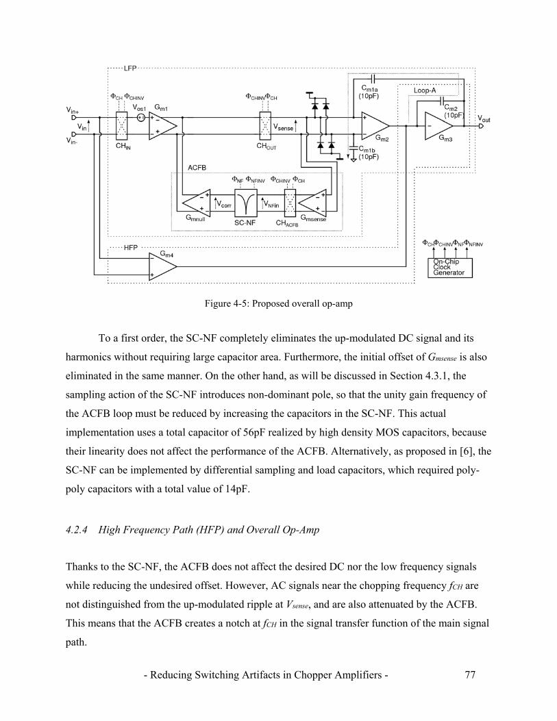
- Reducing Switching Artifacts in Chopper Amplifiers - 77
To a first order, the SC-NF completely eliminates the up-modulated DC signal and its
harmonics without requiring large capacitor area. Furthermore, the initial offset of Gmsense is also
eliminated in the same manner. On the other hand, as will be discussed in Section 4.3.1, the
sampling action of the SC-NF introduces non-dominant pole, so that the unity gain frequency of
the ACFB loop must be reduced by increasing the capacitors in the SC-NF. This actual
implementation uses a total capacitor of 56pF realized by high density MOS capacitors, because
their linearity does not affect the performance of the ACFB. Alternatively, as proposed in [6], the
SC-NF can be implemented by differential sampling and load capacitors, which required poly-
poly capacitors with a total value of 14pF.
4.2.4 High Frequency Path (HFP) and Overall Op-Amp
Thanks to the SC-NF, the ACFB does not affect the desired DC nor the low frequency signals
while reducing the undesired offset. However, AC signals near the chopping frequency fCH are
not distinguished from the up-modulated ripple at Vsense, and are also attenuated by the ACFB.
This means that the ACFB creates a notch at fCH in the signal transfer function of the main signal
path.
Figure 4-5: Proposed overall op-amp

- Reducing Switching Artifacts in Chopper Amplifiers - 78
The notch in the transfer function causes a significant phase shift, leading to instability.
As described in Sections 3.2.2 and 3.2.5, this notch can be bypassed by adding a high frequency
path (HFP) [4,6,14,16]. Figure 4-5 presents a block diagram of the proposed overall op-amp
consisting of a low frequency path (LFP) and the HFP. The LFP is the same circuit presented in
Figure 4-2 including the chopped input transconductor Gm1, the second and output stage
transconductors Gm2 and Gm3, and the ACFB. The HFP consists of a feedforward input
transconductor Gm4 and shares Gm3 with the LFP. The gain of the LFP dominates the overall op-
amp in lower frequencies, but significantly drops at the chopping frequency due to the notch.
The HFP then takes over the transfer function of the overall op-amp, and determines the unity
gain bandwidth fu given by:
2
4
2 m
mu C
Gf
. (4-1)
In order to avoid a pole-zero doublet, the gains of the LFP and HFP must be matched at the
transition frequency by satisfying:
2
4
,1
1
22 m
m
bam
m
C
G
C
G
. (4-2)
Figure 4-6 shows the simulated transfer functions of the LFP, HFP, and the overall op-amp,
which achieves a smooth –20dB/dec roll-off.
Figure 4-6: Simulated transfer functions of the LFP, HFP, and the overall op-amp
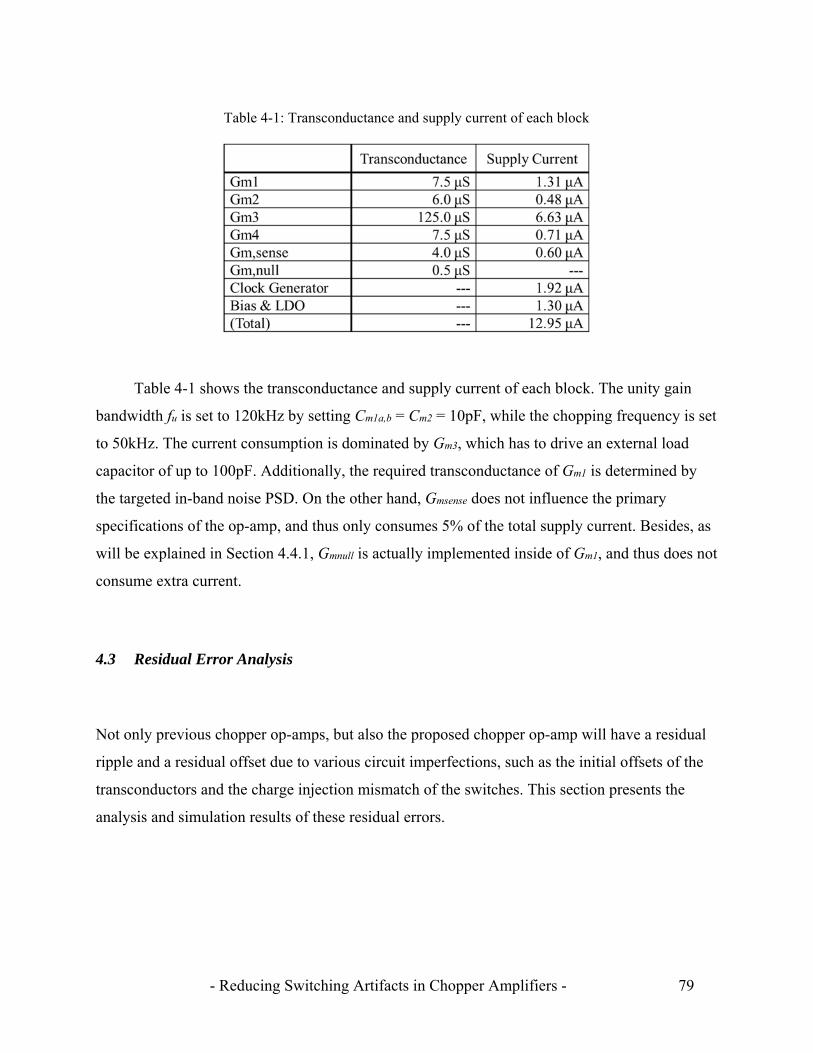
- Reducing Switching Artifacts in Chopper Amplifiers - 79
Table 4-1 shows the transconductance and supply current of each block. The unity gain
bandwidth fu is set to 120kHz by setting Cm1a,b = Cm2 = 10pF, while the chopping frequency is set
to 50kHz. The current consumption is dominated by Gm3, which has to drive an external load
capacitor of up to 100pF. Additionally, the required transconductance of Gm1 is determined by
the targeted in-band noise PSD. On the other hand, Gmsense does not influence the primary
specifications of the op-amp, and thus only consumes 5% of the total supply current. Besides, as
will be explained in Section 4.4.1, Gmnull is actually implemented inside of Gm1, and thus does not
consume extra current.
4.3 Residual Error Analysis
Not only previous chopper op-amps, but also the proposed chopper op-amp will have a residual
ripple and a residual offset due to various circuit imperfections, such as the initial offsets of the
transconductors and the charge injection mismatch of the switches. This section presents the
analysis and simulation results of these residual errors.
Table 4-1: Transconductance and supply current of each block

- Reducing Switching Artifacts in Chopper Amplifiers - 80
4.3.1 ACFB Loop Gain
Similar to the auto-zeroing loop discussed in Section 2.3.2, the ACFB has a finite loop gain
AvACFB which results in residual errors. By using the circuit shown in Figure 4-2, the loop is
broken at the Vcorr nodes, and its gain can be broken down into two parts, i.e. AvACFB ≡
AvACFB1•AvACFB2; AvACFB1 is the gain from the Vcorr to Vsense nodes through Gmnull and CHOUT;
AvACFB2 is the gain from Vsense to the output of the SC-NF through Gmsense and CHACFB.
First, Vcorr is converted into differential currents + Inull/2 and –Inull/2 by Gmnull, and is then
up-modulated by CHOUT. These up-modulated currents are converted into a voltage with an
impedance at the Vsense nodes. At the chopping frequency fCH, this impedance is dominated by the
capacitors Cm1a,b. By assuming that the input of Gm3 is a virtual ground, Kirchhoff’s voltage law
can be applied to a local loop including Cm2, Cm1a, Vsense, and Cm1b (Loop-A in Figure 4-2),
resulting in:
02
22
22 112
2
bmCH
null
senseamCH
null
mCH
sensem
Cfj
I
VCfj
I
Cfj
VG
. (4-3)
By applying Inull = Gmnull•Vcorr, the equation above can be re-formatted to:
2
2,1
2
21
21
1
m
mCH
bam
m
m
mnull
corr
sensevACFB
G
CfjC
C
G
G
V
VA
. (4-4)
By applying the parameters in Table 4-1, AvACFB1 has a 0.07 magnitude (-23dB) and a 32-degree
phase delay.
Next, Vsense is converted into differential currents by Gmsense and is down-modulated by
CHACFB. These down-modulated currents flow into the sampling capacitors CNF1-4, which forms
an integrator. The resulting voltage VNFin will then be sampled by the clocks ΦNF and ΦNFINV.
Since the signal of interests at VNFin is down-modulated, its phase is arbitrary relative to those of
ΦNF and ΦNFINV. Therefore, this sampling action will result in a sinc filter rather than a notch
filter. The resulting gain AvACFB2 is given by:

- Reducing Switching Artifacts in Chopper Amplifiers - 81
CH
CH
NFNFosense
osensemsensevACFB
f
ff
f
CCRjf
RGA
2
2sin
)2(21 6,5,412
, (4-5)
where Rosense is the impedance at the output of Gmsense, which is dominated by the dynamic
switching conductance of CHACFB and results in the DC gain (Gmsense·Rosense) of 64dB.
By combining AvACFB1 and AvACFB2, the overall loop gain AvACFB is 41dB at DC. This gain
first drops with a slope of –20dB/dec due to the dominant pole associated with CNF1-6. It then has
a notch, hence a significant phase shift, at 2fCH due to the sinc filter. Therefore, the unity gain
bandwidth of the ACFB fuACFB must be well below 2fCH to keep the loop stable. As shown in
Figure 4-3, the capacitors are set to CNF1-4 = 7pF and CNF5,6 = 14pF, so that fu,ACFB will be 1.5kHz
while fCH is 50kHz. This fu,ACFB is still high enough to effectively cancel the 1/f noise of Gm1, the
corner frequency of which is 200Hz. Based on Equations (4-4) and (4-5), the calculated AvACFB is
shown in Figure 4-7 along with the simulation result. This simulation was conducted by the
SpectreRF Periodic AC analysis (PAC), which includes the dynamic effects of the chopping and
the SC-NF [17]. The two plots are reasonably correlated, which validates the analysis in this
subsection.
Figure 4-7: Calculated and simulated loop gain of the ACFB
- Reducing Switching Artifacts in Chopper Amplifiers - 82
4.3.2 Residual Ripple
Similar to auto-zeroing, the ACFB suffers from a correction voltage error Vcorrerr due to the finite
loop gain AvACFB and the charge injection mismatch. Similar to Equation (2-6), Vcorrerr is
expressed as:
6,5,41,1
1
1
1
NFNF
NFnullosos
mnull
m
vACFBcorrerr CC
qVV
G
G
AV
, (4-6)
where Vos1 and Vosnull are the initial offsets of Gm1 and Gmnull, respectively, while ΔqNF is the
charge injection mismatch in the SC-NF. Additionally, a sampled noise charge (e.g. kTC noise)
is added along with ΔqNF. For convenience, Vcorrerr can be referred back to the input of Gm1
(VGm1err) by multiplying Gmnull/Gm1, resulting in:
6,5411111 1
1
NFNF
NF
m
mnullosnull
m
mnullos
vACFBerrGm CC
q
G
GV
G
GV
AV
. (4-7)
The initial offset Vos1 is reduced by a factor equal to the loop gain AvACFB, if the charge injection
error is sufficiently reduced by decreasing Gmnull relative to Gm1. This residual error voltage will
be up-modulated by CHOUT and become the output ripple, the amplitude of which can be
obtained by replacing Vos1 with VGm1err in Equations (2-11) and (2-12).
As suggested in Equation (4-4), the loop gain AvACFB decreases due to the presence of the
local feedback around Gm2 and Gm3. Moreover, unlike [14], charge injection mismatch and
sampled noise ΔqNF are added due to the sampling action in the SC-NF. Therefore, the ACFB
will result in a larger residual ripple amplitude and a larger noise PSD peak than the RRL in [14].
4.3.3 Residual Offset
The combined input offset voltage of Gm2 and Gm4 (Vos2 and Vos4) appears at the input of Gm2. In
conjunction with a finite voltage gain of Gm1 (Av1), it will cause a residual offset Vos,res:
- Reducing Switching Artifacts in Chopper Amplifiers - 83
4
2
42
1,
1os
m
mos
vresos V
G
GV
AV . (4-8)
Furthermore, since Gmsense is coupled to the input of Gm2, it converts this offset into a
current along with its own input offset Vos,sense. Similar to the case of the desired input DC signals
discussed in Section 4.2.3, this current is up-modulated by CHACFB and generates a triangular
ripple voltage, the amplitude VNF,rip of which is given by:
senseosos
m
mos
NFCH
msenseripNF VV
G
GV
Cf
GV ,4
2
42
41, 4
. (4-9)
Although this ripple will be filtered by the SC-NF, the ripple amplitude must be small enough
not to affect the operation of Gmsense and not to decrease the DC gain of the Gmsense, because
otherwise the residual output ripple would increase. By applying Vos2 = 7.0mV, Vos4 = 6.5mV,
Vos,sense = 11.0mV, CNF1-4 = 7pF, fCH = 50kHz, and the parameters in Table 4-1, VNF,rip will be
75mV. This amplitude can be reduced by decreasing Gmsense without degrading the primary op-
amp specifications such as the in-band noise or the gain bandwidth. Therefore, CNF1-4 and fCH can
be set relatively low, which will reduce the die size and input bias current. This design flexibility
is a key advantage compared to the SC-NF used in [6], where the ripple amplitude is determined
by the input transconductor in the main signal path.
4.3.4 Summary
Transient simulations were performed to evaluate the output ripple and residual offset. The
transistor-level schematic of Figure 4-5 is applied to unity gain feedback. Table 4-2 shows the
sensitivity to each initial error, where one row represents one simulation result. Input offset was
added to each transconductor, while coupling capacitance mismatch was added to each switch
network. Additionally, a sampling capacitor mismatch was added in the SC-NF. The magnitudes
of these initial errors were set to 4.5σ based on the process characterization data. Also, a 1%
clock skew was given between the chopping ΦCH and SC-NF ΦNF clocks, although the actual
skew was expected to be less.

- Reducing Switching Artifacts in Chopper Amplifiers - 84
Table 4-2: Simulated sensitivity to each initial error
Figure 4-8: Simulated ripple waveforms without and with ACFB
- Reducing Switching Artifacts in Chopper Amplifiers - 85
As suggested by Equations (4-7) and (4-8), the initial offset of Gm1 dominates the residual
ripple, while the initial offsets of Gm2 and Gm4 dominate the residual offset. Additionally, the
charge injection mismatch in CHOUT contributes to the residual offset, as explained in Section
2.4.3. On the other hand, the residual ripple and offset are not sensitive to the errors in the SC-
NF including the charge injection mismatch, the sampling capacitor mismatch, and the clock
skew, since these errors are suppressed by the ACFB.
The simulation was also performed with all the initial error sources, and the resulting
performance is shown in the bottom row in Table 4-2 while the transient waveform is shown in
Figure 4-8. The residual ripple and offset are 42.9Vrms and 7.8V, respectively. Additionally,
the circuit without the ACFB was also simulated for comparison, which resulted in a 5.9mVrms
residual ripple and a –43V residual offset. By taking the ratio of these two ripple amplitudes,
the ripple reduction factor achieved by the ACFB is specified as 42.7dB.
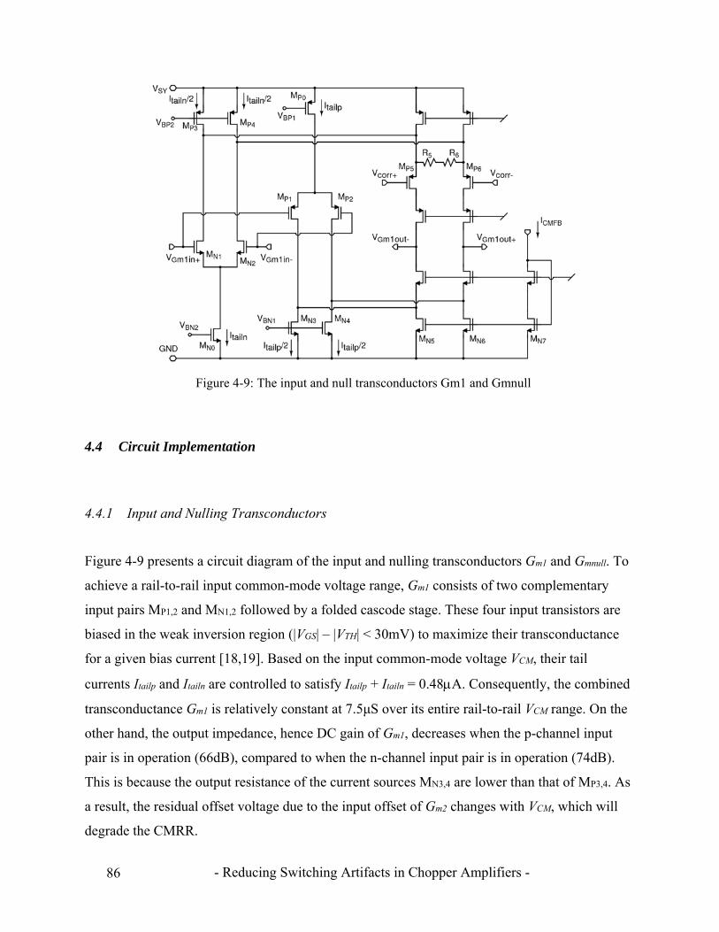
- Reducing Switching Artifacts in Chopper Amplifiers - 86
4.4 Circuit Implementation
4.4.1 Input and Nulling Transconductors
Figure 4-9 presents a circuit diagram of the input and nulling transconductors Gm1 and Gmnull. To
achieve a rail-to-rail input common-mode voltage range, Gm1 consists of two complementary
input pairs MP1,2 and MN1,2 followed by a folded cascode stage. These four input transistors are
biased in the weak inversion region (|VGS| – |VTH| < 30mV) to maximize their transconductance
for a given bias current [18,19]. Based on the input common-mode voltage VCM, their tail
currents Itailp and Itailn are controlled to satisfy Itailp + Itailn = 0.48A. Consequently, the combined
transconductance Gm1 is relatively constant at 7.5μS over its entire rail-to-rail VCM range. On the
other hand, the output impedance, hence DC gain of Gm1, decreases when the p-channel input
pair is in operation (66dB), compared to when the n-channel input pair is in operation (74dB).
This is because the output resistance of the current sources MN3,4 are lower than that of MP3,4. As
a result, the residual offset voltage due to the input offset of Gm2 changes with VCM, which will
degrade the CMRR.
Figure 4-9: The input and null transconductors Gm1 and Gmnull
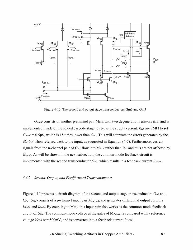
- Reducing Switching Artifacts in Chopper Amplifiers - 87
Gmnull consists of another p-channel pair MP5,6 with two degeneration resistors R5,6, and is
implemented inside of the folded cascode stage to re-use the supply current. R5,6 are 2M to set
Gmnull = 0.5μS, which is 15 times lower than Gm1. This will attenuate the errors generated by the
SC-NF when referred back to the input, as suggested in Equation (4-7). Furthermore, current
signals from the n-channel pair of Gm1 flow into MP5,6 rather than R1, and thus are not affected by
Gmnull. As will be shown in the next subsection, the common-mode feedback circuit is
implemented with the second transconductor Gm2, which results in a feedback current ICMFB.
4.4.2 Second, Output, and Feedforward Transconductors
Figure 4-10 presents a circuit diagram of the second and output stage transconductors Gm2 and
Gm3. Gm2 consists of a p-channel input pair MP21,22, and generates differential output currents
IGm2+ and IGm2-. By coupling to MP23, this input pair also works as the common-mode feedback
circuit of Gm1. The common-mode voltage at the gates of MP21,22 is compared with a reference
voltage VCMREF = 500mV, and is converted into a feedback current ICMFB.
Figure 4-10: The second and output stage transconductors Gm2 and Gm3
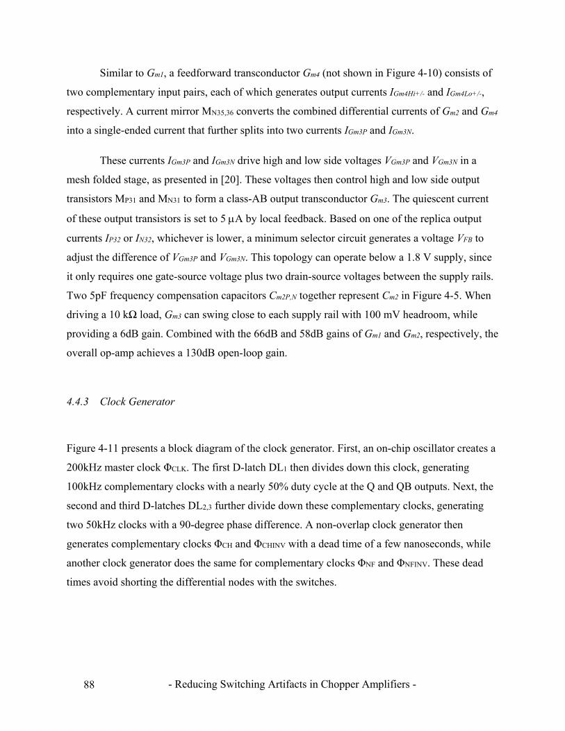
- Reducing Switching Artifacts in Chopper Amplifiers - 88
Similar to Gm1, a feedforward transconductor Gm4 (not shown in Figure 4-10) consists of
two complementary input pairs, each of which generates output currents IGm4Hi+/- and IGm4Lo+/-,
respectively. A current mirror MN35,36 converts the combined differential currents of Gm2 and Gm4
into a single-ended current that further splits into two currents IGm3P and IGm3N.
These currents IGm3P and IGm3N drive high and low side voltages VGm3P and VGm3N in a
mesh folded stage, as presented in [20]. These voltages then control high and low side output
transistors MP31 and MN31 to form a class-AB output transconductor Gm3. The quiescent current
of these output transistors is set to 5 A by local feedback. Based on one of the replica output
currents IP32 or IN32, whichever is lower, a minimum selector circuit generates a voltage VFB to
adjust the difference of VGm3P and VGm3N. This topology can operate below a 1.8 V supply, since
it only requires one gate-source voltage plus two drain-source voltages between the supply rails.
Two 5pF frequency compensation capacitors Cm2P,N together represent Cm2 in Figure 4-5. When
driving a 10 kΩ load, Gm3 can swing close to each supply rail with 100 mV headroom, while
providing a 6dB gain. Combined with the 66dB and 58dB gains of Gm1 and Gm2, respectively, the
overall op-amp achieves a 130dB open-loop gain.
4.4.3 Clock Generator
Figure 4-11 presents a block diagram of the clock generator. First, an on-chip oscillator creates a
200kHz master clock ΦCLK. The first D-latch DL1 then divides down this clock, generating
100kHz complementary clocks with a nearly 50% duty cycle at the Q and QB outputs. Next, the
second and third D-latches DL2,3 further divide down these complementary clocks, generating
two 50kHz clocks with a 90-degree phase difference. A non-overlap clock generator then
generates complementary clocks ΦCH and ΦCHINV with a dead time of a few nanoseconds, while
another clock generator does the same for complementary clocks ΦNF and ΦNFINV. These dead
times avoid shorting the differential nodes with the switches.
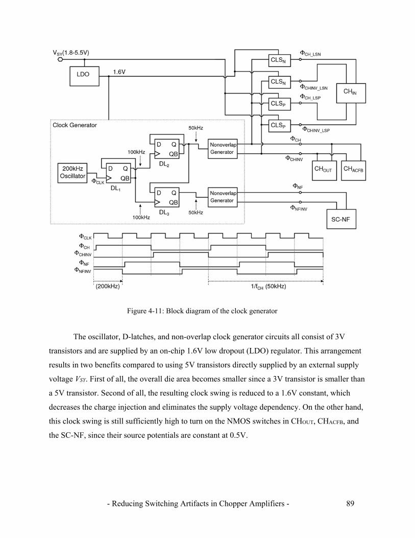
- Reducing Switching Artifacts in Chopper Amplifiers - 89
The oscillator, D-latches, and non-overlap clock generator circuits all consist of 3V
transistors and are supplied by an on-chip 1.6V low dropout (LDO) regulator. This arrangement
results in two benefits compared to using 5V transistors directly supplied by an external supply
voltage VSY. First of all, the overall die area becomes smaller since a 3V transistor is smaller than
a 5V transistor. Second of all, the resulting clock swing is reduced to a 1.6V constant, which
decreases the charge injection and eliminates the supply voltage dependency. On the other hand,
this clock swing is still sufficiently high to turn on the NMOS switches in CHOUT, CHACFB, and
the SC-NF, since their source potentials are constant at 0.5V.
Figure 4-11: Block diagram of the clock generator
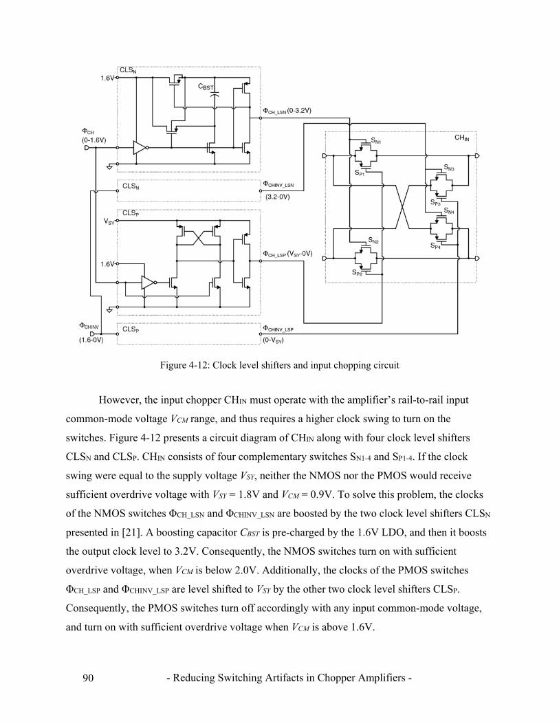
- Reducing Switching Artifacts in Chopper Amplifiers - 90
However, the input chopper CHIN must operate with the amplifier’s rail-to-rail input
common-mode voltage VCM range, and thus requires a higher clock swing to turn on the
switches. Figure 4-12 presents a circuit diagram of CHIN along with four clock level shifters
CLSN and CLSP. CHIN consists of four complementary switches SN1-4 and SP1-4. If the clock
swing were equal to the supply voltage VSY, neither the NMOS nor the PMOS would receive
sufficient overdrive voltage with VSY = 1.8V and VCM = 0.9V. To solve this problem, the clocks
of the NMOS switches ΦCH_LSN and ΦCHINV_LSN are boosted by the two clock level shifters CLSN
presented in [21]. A boosting capacitor CBST is pre-charged by the 1.6V LDO, and then it boosts
the output clock level to 3.2V. Consequently, the NMOS switches turn on with sufficient
overdrive voltage, when VCM is below 2.0V. Additionally, the clocks of the PMOS switches
ΦCH_LSP and ΦCHINV_LSP are level shifted to VSY by the other two clock level shifters CLSP.
Consequently, the PMOS switches turn off accordingly with any input common-mode voltage,
and turn on with sufficient overdrive voltage when VCM is above 1.6V.
Figure 4-12: Clock level shifters and input chopping circuit
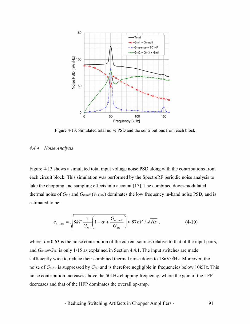
- Reducing Switching Artifacts in Chopper Amplifiers - 91
4.4.4 Noise Analysis
Figure 4-13 shows a simulated total input voltage noise PSD along with the contributions from
each circuit block. This simulation was performed by the SpectreRF periodic noise analysis to
take the chopping and sampling effects into account [17]. The combined down-modulated
thermal noise of Gm1 and Gmnull (en,Gm1) dominates the low frequency in-band noise PSD, and is
estimated to be:
HznVG
G
GkTe
m
nullm
mGmn /871
18
1
,
11,
, (4-10)
where 0.63 is the noise contribution of the current sources relative to that of the input pairs,
and Gmnull/Gm1 is only 1/15 as explained in Section 4.4.1. The input switches are made
sufficiently wide to reduce their combined thermal noise down to 18nV/√Hz. Moreover, the
noise of Gm2-4 is suppressed by Gm1 and is therefore negligible in frequencies below 10kHz. This
noise contribution increases above the 50kHz chopping frequency, where the gain of the LFP
decreases and that of the HFP dominates the overall op-amp.
Figure 4-13: Simulated total noise PSD and the contributions from each block

- Reducing Switching Artifacts in Chopper Amplifiers - 92
The noise of Gmsense and the SC-NF are up-modulated, thus resulting in a high noise PSD at
the 50kHz chopping frequency. The magnitude of this peak PSD is 125nV/√Hz, which is only
increased by a factor of 1.44 √2 compared to the 87nV/√Hz noise floor. Similar to the slow
auto-zeroing technique presented in [12], the peak PSD is reduced by setting the loop bandwidth
of the ACFB (fu,ACFB = 1.5kHz) much lower than the sampling frequency of the SC-NF. In this
case, the overall spectrum at 50kHz will be dominated by the up-modulated residual offset,
which is estimated in Table 4-2 but is not included in this noise simulation.
4.5 Measurement Results
The proposed op-amp has been fabricated in a 0.35μm CMOS process augmented by 5V CMOS
transistors. Figure 4-14 shows a die micrograph with the entire area, covering 0.64 mm2, only
8% of which is occupied by the ACFB including Gmsense, Gmnull, and the SC-NF. As described in
Section 4.4.3, the clock generator consists of 3V transistors and is supplied by the on-chip 1.6V
LDO. All the other circuits consist of 5V transistors and are directly supplied by the external
supply. The op-amp only draws 13μA from a 1.8V to 5.5 V supply voltage VSY, and has a rail-to-
rail input common-mode voltage VCM range and a –40°C to 125°C temperature range.
Figure 4-14: Die micrograph of the op-amp

- Reducing Switching Artifacts in Chopper Amplifiers - 93
Figure 4-15 shows the input offset voltages of 20 op-amp units over the rail-to-rail VCM
range with VSY = 1.8V. The offset increases in the range of VCM = 0 to 1.2V, where the gain of
Gm1 decreases with the p-channel input pair, as explained in Section 4.4.1. In this subsection, the
measurement data are obtained with VSY = 1.8V and VCM = 0.9V unless otherwise stated. Figure
4-16 (a) and (b) shows the histograms of the offset voltage and the temperature drift,
respectively. The ±6.4V maximum offset in the histogram is well correlated with the ±7.8V
simulated maximum offset shown in Table 4-2. Offset data are also obtained with VSY = 5.5V and
VCM at each supply rail, specifying a 120dB minimum DC PSRR and a 115dB minimum CMRR.
Figure 4-15: Offset voltages over the rail-to-rail VCM range
Figure 4-16: Histograms of (a) the offset voltage and (b) the temperature drift
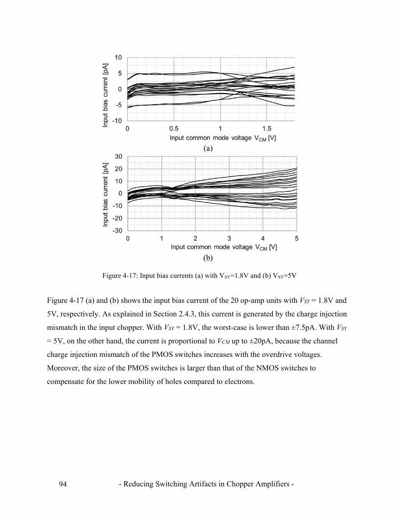
- Reducing Switching Artifacts in Chopper Amplifiers - 94
Figure 4-17 (a) and (b) shows the input bias current of the 20 op-amp units with VSY = 1.8V and
5V, respectively. As explained in Section 2.4.3, this current is generated by the charge injection
mismatch in the input chopper. With VSY = 1.8V, the worst-case is lower than ±7.5pA. With VSY
= 5V, on the other hand, the current is proportional to VCM up to ±20pA, because the channel
charge injection mismatch of the PMOS switches increases with the overdrive voltages.
Moreover, the size of the PMOS switches is larger than that of the NMOS switches to
compensate for the lower mobility of holes compared to electrons.
Figure 4-17: Input bias currents (a) with VSY=1.8V and (b) VSY=5V
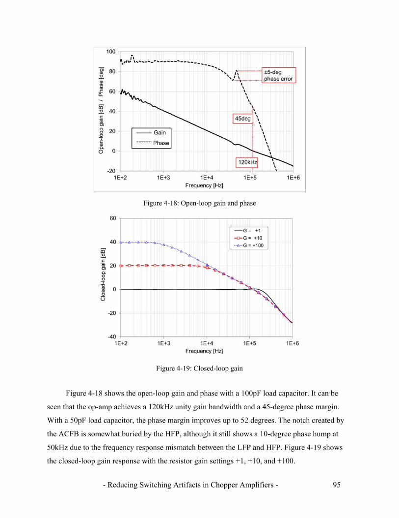
- Reducing Switching Artifacts in Chopper Amplifiers - 95
Figure 4-18 shows the open-loop gain and phase with a 100pF load capacitor. It can be
seen that the op-amp achieves a 120kHz unity gain bandwidth and a 45-degree phase margin.
With a 50pF load capacitor, the phase margin improves up to 52 degrees. The notch created by
the ACFB is somewhat buried by the HFP, although it still shows a 10-degree phase hump at
50kHz due to the frequency response mismatch between the LFP and HFP. Figure 4-19 shows
the closed-loop gain response with the resistor gain settings +1, +10, and +100.
Figure 4-18: Open-loop gain and phase
Figure 4-19: Closed-loop gain
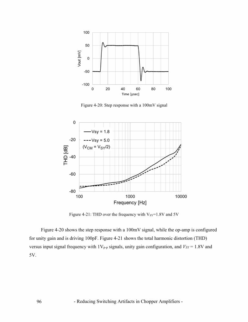
- Reducing Switching Artifacts in Chopper Amplifiers - 96
Figure 4-20 shows the step response with a 100mV signal, while the op-amp is configured
for unity gain and is driving 100pF. Figure 4-21 shows the total harmonic distortion (THD)
versus input signal frequency with 1Vp-p signals, unity gain configuration, and VSY = 1.8V and
5V.
Figure 4-20: Step response with a 100mV signal
Figure 4-21: THD over the frequency with VSY=1.8V and 5V
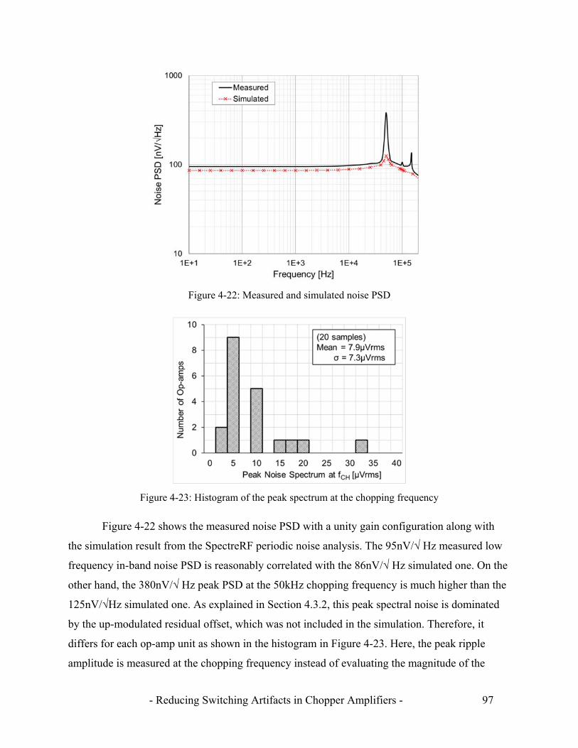
- Reducing Switching Artifacts in Chopper Amplifiers - 97
Figure 4-22 shows the measured noise PSD with a unity gain configuration along with
the simulation result from the SpectreRF periodic noise analysis. The 95nV/√ Hz measured low
frequency in-band noise PSD is reasonably correlated with the 86nV/√ Hz simulated one. On the
other hand, the 380nV/√ Hz peak PSD at the 50kHz chopping frequency is much higher than the
125nV/√Hz simulated one. As explained in Section 4.3.2, this peak spectral noise is dominated
by the up-modulated residual offset, which was not included in the simulation. Therefore, it
differs for each op-amp unit as shown in the histogram in Figure 4-23. Here, the peak ripple
amplitude is measured at the chopping frequency instead of evaluating the magnitude of the
Figure 4-22: Measured and simulated noise PSD
Figure 4-23: Histogram of the peak spectrum at the chopping frequency
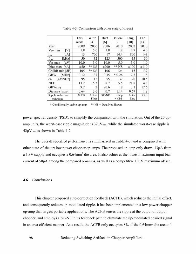
- Reducing Switching Artifacts in Chopper Amplifiers - 98
power spectral density (PSD), to simplify the comparison with the simulation. Out of the 20 op-
amp units, the worst-case ripple magnitude is 32μVrms, while the simulated worst-case ripple is
42μVrms as shown in Table 4-2.
The overall specified performance is summarized in Table 4-3, and is compared with
other state-of-the-art low power chopper op-amps. The proposed op-amp only draws 13μA from
a 1.8V supply and occupies a 0.64mm2 die area. It also achieves the lowest maximum input bias
current of 50pA among the compared op-amps, as well as a competitive 10μV maximum offset.
4.6 Conclusions
This chapter proposed auto-correction feedback (ACFB), which reduces the initial offset,
and consequently reduces up-modulated ripple. It has been implemented in a low power chopper
op-amp that targets portable applications. The ACFB senses the ripple at the output of output
chopper, and employs a SC-NF in its feedback path to eliminate the up-modulated desired signal
in an area efficient manner. As a result, the ACFB only occupies 8% of the 0.64mm2 die area of
Table 4-3: Comparison with other state-of-the-art
- Reducing Switching Artifacts in Chopper Amplifiers - 99
the overall op-amp. On the other hand, its maximum residual ripple of 32μVrms is relatively
large, due to the limited loop gain of the ACFB and to the presence of the charge injection
mismatch and sampled noise in the SC-NF. Although it can be attenuated by an external low-
pass filter for low frequency applications, it should be improved for applications which require
relatively wide signal bandwidth.
Compared to the implementation in [6], which uses a SC-NF in the main signal path, the
ACFB requires two extra transconductors to sense the ripple and to null the initial offset,
although they only consume 5% of the total current. On the other hand, the ACFB offers
flexibility in choosing a relatively low chopping frequency, which reduces the input bias current.
Moreover, the sampled noise in the SC-NF is up-modulated and thus does not contribute to the
resulting in-band noise PSD.

- Reducing Switching Artifacts in Chopper Amplifiers - 100
4.7 References
[1] M. W. Hann, “Ultra Low Power, 18 bit Precision ECG Data Acquisition System”, June 2013,
Accessed on March 2018, [Online] Available: <http://www.ti.com/lit/ug/slau516/slau516.pdf>.
[2] R. F. Yazicioglu, P. Merken, R. Puers, and C. V. Hoof, “A 60 W 60 nV/√Hz Readout Front-
End for Portable Biopotential Acquisition Systems”, IEEE J. Solid-State Circuits, vol. 42, no. 5,
pp. 1100-1110, May 2007.
[3] R. F. Yazicioglu, P. Merken, R. Puers, and C. V. Hoof, “A 200 W Eight-Channel EEG
Acquisition ASIC for Ambulatory EEG Systems”, IEEE J. Solid-State Circuits, vol. 43, no. 12,
pp. 3025-3038, Dec. 2008.
[4] J. F. Witte, K. A. A. Makinwa, and J. H. Huijsing, “A CMOS Chopper Offset-Stabilized
Opamp”, IEEE J. Solid-State Circuits, vol. 42, no. 7, pp. 1529-1535, July 2007.
[5] A. Bakker and J.H. Huijsing, “A CMOS Chopper Opamp with Integrated Low-Pass Filter”,
Proc. of IEEE ESSCIRC, pp. 200-203, Sept. 1997.
[6] R. Burt and J. Zhang, “A Micropower Chopper-Stabilized Operational Amplifier using a SC
Notch Filter with Synchronous Integration inside the Continuous-Time Signal Path”, IEEE J.
Solid-State Circuits, vol. 41, no. 12, pp. 2729-2736, Dec. 2006.
[7] Texas Instruments, “OPA333 Datasheet”, Mar. 2006, Accessed on March 2018, [Online]
Available: <http://www.ti.com/lit/gpn/opa333>.
[8] A. Bilotti and G. Monreal, “Chopper-Stabilized Amplifiers with a Track-and-Hold Signal
Demodulator”, IEEE Transactions on Circuits and Systems, vol. 46, no. 4, pp. 490-495, Apr.
1999.
[9] M. Belloni, E. Bonizzoni, A. Fornasari, and F. Maloberti, “A Micropower Chopper-CDS
Operational Amplifier”, IEEE J. Solid-State Circuits, vol. 45, no. 12, pp. 2521-2529, Dec. 2010.
- Reducing Switching Artifacts in Chopper Amplifiers - 101
[10] A. T. K. Tang, “A 3V-Offset Operational Amplifier with 20nV/√Hz Input Noise PSD at
DC Employing both Chopping and Autozeroing”, IEEE ISSCC Dig. Tech. Papers, pp. 362-387,
Feb. 2002.
[11] Analog Devices, “AD8628 Datasheet”, 2002, Accessed on March 2018, [Online] Available:
<http://www.analog.com/media/en/technical-documentation/data-
sheets/AD8628_8629_8630.pdf>.
[12] M. Pertijs and W. J. Kindt, “A 140 dB-CMRR current-feedback instrumentation amplifier
employing ping-pong auto-zeroing and chopping”, IEEE J. Solid-State Circuits, vol. 45, no. 10,
pp.2044-2056, Oct. 2010.
[13] R. Wu, K. A. A. Makinwa, and J. H. Huijsing, “A Chopper Current-Feedback
Instrumentation Amplifier with a 1 mHz 1/f Noise Corner and an AC-Coupled Ripple Reduction
Loop”, IEEE J. Solid-State Circuits, vol. 44, no. 12, pp. 3232-3243, Dec. 2009.
[14] Q. Fan, J. H. Huijsing, and K.A.A. Makinwa, “A 21 nV/√Hz Chopper-Stabilized Multi-Path
Current-Feedback Instrumentation Amplifier With 2 µV Offset”, IEEE J. Solid-State Circuits,
vol. 47, no. 2, pp. 464-475, Feb. 2012.
[15] J. Xu, R. F. Yazicioglu, P. Harpe, K. A. A. Makinwa, and C. V. Hoof, “A 160µW 8-
Channel Active Electrode System for EEG Monitoring”, IEEE ISSCC Dig. Tech. Papers, pp.
300-301, Feb. 2011.
[16] R. G. H. Eschauzier, L. P. T. Kerklaan, and J. H. Huijsing, “A 100-MHz 100-dB
Operational Amplifier with Multipath Nested Miller Compensation Structure”, IEEE J. Solid-
State Circuits, vol. 27, no. 12, pp. 1709-1717, Dec. 1992.
[17] K. Kundert, “Simulating Switched-Capacitor Filters with SpectreRF”, July 2006, Accessed
on March 2018, [Online] Available: <http://www.designers-guide.org/Analysis/sc-filters.pdf>.
[18] E. Vittoz and J. Fellrath, “CMOS Analog Integrated Circuits Based on Weak Inversion
Operation”, IEEE J. Solid-State Circuits, vol. 12, no. 3, pp. 224-231, June 1977.
- Reducing Switching Artifacts in Chopper Amplifiers - 102
[19] W. Sansen, “Minimum Power in Analog Amplifying Blocks”, IEEE Solid-State Circuits
Magazine, pp. 83-89, Fall 2015.
[20] K-J. Langen and J. H. Huijsing, “Compact Low-Voltage Power-Efficient Operational
Amplifier Cells for VLSI”, IEEE J. Solid-State Circuits, vol. 33, no. 10, pp. 1482-1496, Oct.
1998.
[21] G. Palmisano and G. Palumbo, “Clock Boosters for 1.2-V SC Circuits”, IEEE International
Symposium on Circuits and Systems Tech. Papers, pp. 2012-2015, June 1997.
- Reducing Switching Artifacts in Chopper Amplifiers - 103
Chapter 5
Chopper Op-Amp with Adaptive Clock Boosting
Technique2
This chapter presents a 5.6nV/√Hz chopper op-amp realized in a 0.35m CMOS process
augmented by 5V CMOS transistors. Additionally, circuit techniques are proposed to relax the
design trade-offs between noise PSD, power consumption, die area, and residual offset, as
discussed in Chapter 2. Consequently, the op-amp also achieves a 0.5V maximum offset and a
15nV/°C maximum offset drift over the amplifier’s entire rail-to-rail input common-mode
voltage range, while drawing 1.4mA from a 2.1-5.5V supply and occupying a die area of
1.26mm2.
After describing the motivation for the design in Section 5.1, the overall op-amp
configuration is presented in Section 5.2. Frequency compensation is realized in a power and
area efficient manner by using a current attenuator and a dummy differential output. In addition,
the up-modulated ripple is suppressed by the auto-correction feedback (ACFB) technique
presented in Chapter 4. In Section 5.3, the circuit design of the transconductors is presented as
well as the noise analysis. Section 5.4 discusses the input chopper and the trade-off between
noise PSD and residual offset. It then proposes an adaptive clock boosting technique to drive the
NMOS input switches over the amplifier’s rail-to-rail common-mode voltage range with a
constant overdrive voltage. This minimizes their charge injection and eliminates its common-
mode voltage dependency, to achieve low noise, low offset, and high CMRR. The measurement
results are discussed in Section 5.5, and the chapter ends with a conclusion in Section 5.6.
______________________
2 This chapter is derived from a journal publication of the author: Y. Kusuda, “A 5.6 nV/√Hz Chopper Operational
Amplifier Achieving a 0.5 V Maximum Offset Over Rail-to-Rail Input Range with Adaptive Clock Boosting
Technique”, IEEE J. Solid-State Circuits, vol. 51, no. 9, pp. 2119-2128, Sept. 2016.
- Reducing Switching Artifacts in Chopper Amplifiers - 104
5.1 Motivation
As described in Section 1.4.1, precision op-amps are often configured for closed-loop gains
higher than hundred in sensor signal conditioning application [1]. In this case, low offset and low
in-band noise are required to minimize the total output error. Buffers for precision references or
precision DAC outputs described in Section 1.5.2 are another application [2], in which an op-
amp with a wide (ideally rail-to-rail) input common-mode range is required. To cover both these
applications, such an op-amp should also provide microvolt-level input offset and low in-band
noise over a wide supply voltage, input common-mode voltage, and temperature range. While
chopping can be applied to reduce the offset and 1/f noise, the resulting up-modulated ripple
must be reduced to achieve a wide usable signal bandwidth, especially in buffer applications.
Lowering the in-band noise PSD of a chopper op-amp often compromises other
specifications. First, the input transconductance must be increased. Consequently, the frequency
compensation capacitors, the transconductances of the subsequent stages, or both, need to be
increased to maintain stability. This further increases supply current, die area, or both. Second, as
explained in Section 2.4.3, the input chopping switches must be made sufficiently wide to reduce
their on-resistance and hence their thermal noise, but which will increase residual offset [3,4].
Moreover, when conventional CMOS switches are used, both their charge injection and on-
resistance vary with both the supply and the input common-mode voltages. This degrades the
worst-case residual offset voltage as well as the CMRR and the PSRR, especially when rail-to-
rail input common-mode voltage range is required at low supply voltages.
Most previous chopper op-amps have more than 10nV/√Hz input noise PSDs [5-11],
while achieving maximum offsets ranging from 10V down to 1V. A 6nV/√Hz conditionally
stable chopper op-amp with a 10V maximum offset was reported in [12,13], in which a multi-
pole feedforward compensation technique is used. Later, in [14], a 6.2nV/√Hz chopper op-amp
with a 5.5V maximum offset was realized, with a minimum supply voltage of 2.7V but whose
input common-mode voltage range does not include the positive supply rail.
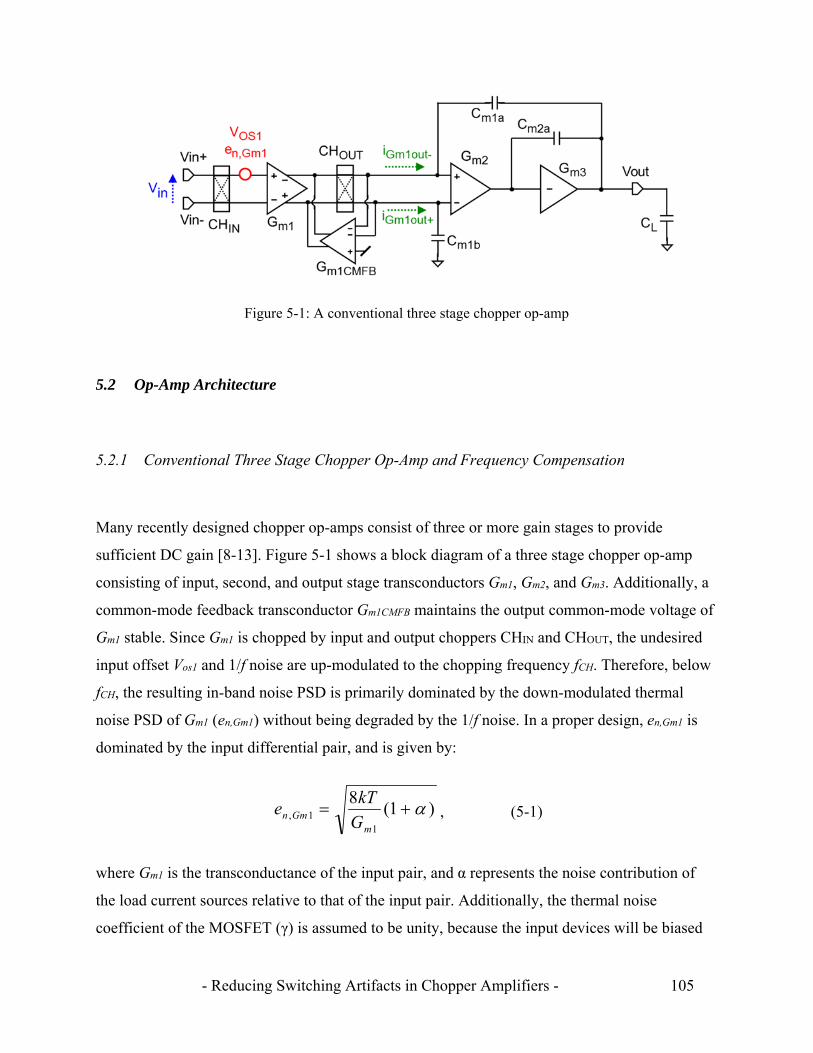
- Reducing Switching Artifacts in Chopper Amplifiers - 105
5.2 Op-Amp Architecture
5.2.1 Conventional Three Stage Chopper Op-Amp and Frequency Compensation
Many recently designed chopper op-amps consist of three or more gain stages to provide
sufficient DC gain [8-13]. Figure 5-1 shows a block diagram of a three stage chopper op-amp
consisting of input, second, and output stage transconductors Gm1, Gm2, and Gm3. Additionally, a
common-mode feedback transconductor Gm1CMFB maintains the output common-mode voltage of
Gm1 stable. Since Gm1 is chopped by input and output choppers CHIN and CHOUT, the undesired
input offset Vos1 and 1/f noise are up-modulated to the chopping frequency fCH. Therefore, below
fCH, the resulting in-band noise PSD is primarily dominated by the down-modulated thermal
noise PSD of Gm1 (en,Gm1) without being degraded by the 1/f noise. In a proper design, en,Gm1 is
dominated by the input differential pair, and is given by:
)1(8
11,
mGmn G
kTe , (5-1)
where Gm1 is the transconductance of the input pair, and α represents the noise contribution of
the load current sources relative to that of the input pair. Additionally, the thermal noise
coefficient of the MOSFET (γ) is assumed to be unity, because the input devices will be biased
Figure 5-1: A conventional three stage chopper op-amp
- Reducing Switching Artifacts in Chopper Amplifiers - 106
in the weak inversion region (|VGS| – |VTH| < 30mV) to maximize their transconductance for a
given bias current [8-11].
In the time domain, the differential output currents of Gm1 (iGm1out+ and iGm1out-) will
include both a signal component vin(t) and a noise component en,Gm1(t):
)(2
)(2
)( 1,11
1 teG
tvG
ti Gmnm
inm
outGm (5-2)
)(2
)(2
)( 1,11
1 teG
tvG
ti Gmnm
inm
outGm (5-3)
Note that the common-mode noise at the output of Gm1 is cancelled by Gm1CMFB, so that en,Gm1
complementarily contributes to iGm1out+ and iGm1out-. Although Gm1CMFB itself generates common-
mode noise at the output of Gm1, this noise will be rejected by Gm2 with its high CMRR.
Nested Miller frequency compensation is realized by capacitors Cm1a, Cm1b, and Cm2a,
while CL is an external load capacitor. According to [15], the unity gain bandwidth fu, second
pole fp2, and third pole fp3 of the op-amp are given by:
bam
mu C
Gf
,1
1
2
(5-4)
am
mp C
Gf
2
22 2
(5-5)
L
mp C
Gf
23
3 . (5-6)
These pole frequencies should satisfy fp3 ≥ 2 fp2 ≥ 4 fu, to obtain a 60-degree phase margin, and to
maintain the stability. However, to reduce the thermal noise in Equation (5-1), Gm1 must be
significantly increased due to the square root relation, resulting in a much higher fu.
Consequently, Gm2 and Gm3 must be increased as well to maintain the stability, which further
increases the overall current consumption. Alternatively, Cm1a,b can be increased to reduce fu at
the cost of die area.
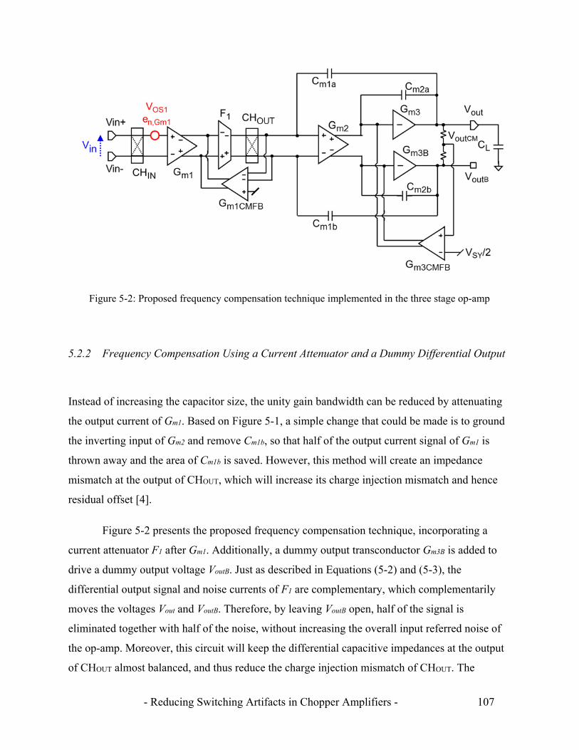
- Reducing Switching Artifacts in Chopper Amplifiers - 107
5.2.2 Frequency Compensation Using a Current Attenuator and a Dummy Differential Output
Instead of increasing the capacitor size, the unity gain bandwidth can be reduced by attenuating
the output current of Gm1. Based on Figure 5-1, a simple change that could be made is to ground
the inverting input of Gm2 and remove Cm1b, so that half of the output current signal of Gm1 is
thrown away and the area of Cm1b is saved. However, this method will create an impedance
mismatch at the output of CHOUT, which will increase its charge injection mismatch and hence
residual offset [4].
Figure 5-2 presents the proposed frequency compensation technique, incorporating a
current attenuator F1 after Gm1. Additionally, a dummy output transconductor Gm3B is added to
drive a dummy output voltage VoutB. Just as described in Equations (5-2) and (5-3), the
differential output signal and noise currents of F1 are complementary, which complementarily
moves the voltages Vout and VoutB. Therefore, by leaving VoutB open, half of the signal is
eliminated together with half of the noise, without increasing the overall input referred noise of
the op-amp. Moreover, this circuit will keep the differential capacitive impedances at the output
of CHOUT almost balanced, and thus reduce the charge injection mismatch of CHOUT. The
Figure 5-2: Proposed frequency compensation technique implemented in the three stage op-amp
- Reducing Switching Artifacts in Chopper Amplifiers - 108
reduced unity gain bandwidth fu' is given by:
2
1
2 ,1
11
bam
mu C
FGf
. (5-7)
However, the noise of F1 can significantly contribute to the overall input noise, if the
signal is attenuated too much. To avoid this scenario, the proposed design sets F1 = 0.25 and Gm1
= 3.2mS. It also targets fu' = 4MHz to reduce the required current consumption in Gm2 and Gm3.
According to Equation (5-7), this then requires Cm1a,b = 16pF, which would be eight times larger
with the conventional circuit shown in Figure 5-1. Based on Equations (5-4), (5-5) and (5-6), the
second and third poles are set to fp2 = 8MHz and fp3 = 16MHz when driving CL = 100pF. On the
other hand, the internal capacitor at VoutB is only 10pF, which sets the pole at this node fp3B =
40MHz. The difference between fp3 and fp3B creates a slight transient response mismatch between
Vout and VoutB. However, it will hardly affect the overall settling of the op-amp, since both of its
frequency poles are sufficiently higher than fu’.
This dummy differential output technique requires additional circuitry, including Gm3B, an
output common-mode feedback transconductor Gm3CMFB, and a capacitor Cm2b. Gm3CMFB
compares the output common-mode voltage VoutCM with VSY/2 and provides feedback currents to
the inputs of Gm3 and Gm3B. This common-mode feedback loop bandwidth can be lower than fu'
without compromising the bandwidth of the overall op-amp, as long as VoutCM is not affected by
any input signal. This can be achieved by designing F1 to have fully complementary output
currents without any common-mode components. Additionally, the transconductance of Gm3B is
made four times lower than that of Gm3, since it does not drive external loads. The comparison
for design parameters in Figure 5-1 and Figure 5-2 will be given in Section 5.3.2 after the
detailed noise analysis.
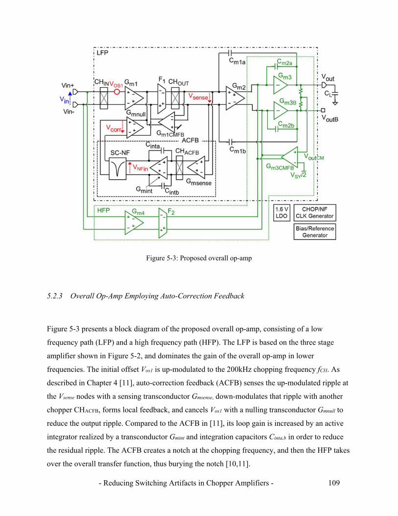
- Reducing Switching Artifacts in Chopper Amplifiers - 109
5.2.3 Overall Op-Amp Employing Auto-Correction Feedback
Figure 5-3 presents a block diagram of the proposed overall op-amp, consisting of a low
frequency path (LFP) and a high frequency path (HFP). The LFP is based on the three stage
amplifier shown in Figure 5-2, and dominates the gain of the overall op-amp in lower
frequencies. The initial offset Vos1 is up-modulated to the 200kHz chopping frequency fCH. As
described in Chapter 4 [11], auto-correction feedback (ACFB) senses the up-modulated ripple at
the Vsense nodes with a sensing transconductor Gmsense, down-modulates that ripple with another
chopper CHACFB, forms local feedback, and cancels Vos1 with a nulling transconductor Gmnull to
reduce the output ripple. Compared to the ACFB in [11], its loop gain is increased by an active
integrator realized by a transconductor Gmint and integration capacitors Cinta,b in order to reduce
the residual ripple. The ACFB creates a notch at the chopping frequency, and then the HFP takes
over the overall transfer function, thus burying the notch [10,11].
Figure 5-3: Proposed overall op-amp

- Reducing Switching Artifacts in Chopper Amplifiers - 110
5.2.4 ACFB Loop Gain Including Active Integrator
Figure 5-4 presents a circuit diagram of Gmsense, as well as the active integrator realized by Gmint
and Cinta,b. Gsense consists of a p-channel input pair MP51,52, while Gmint consists of a pseudo
differential transconductor realized by two common-source transistors MN61,62. The common-
mode feedback transconductor GmintCMFB consists of four source-coupled PMOS transistors MP61-
64, which compare the output common-mode voltage of Gmint (VNFin+ and VNFin-) with a 0.625V
reference, and then adjusts the bias currents of MN51 and MN52. MP61-64 are de-generated by
resistors to expand their differential input range, so that the common-mode voltage of VNFin+ and
VNFin- can be still detected even in the presence of ripple.
The differential output of Gmint (VNFin) drives a switched capacitor notch filter (SC-NF)
which consists of the same topology as the one shown in Figure 4-3, but CNF1-4 = 1pF and CNF5,6
= 2pF are used. The clock timings ΦNF and ΦNFINV operate at the same 200kHz frequency as the
chopping clocks ΦCH and ΦCHINV but with a 90-degree phase difference, so that the desired in-
band signals are up-modulated by CHACFB and then rejected by the SC-NF.
As analyzed in Section 4.3.1, the loop gain of the ACFB (AvACFB) can be broken into two
Figure 5-4: The ripple sensing transconductor Gmsense and the active integrator Gmint
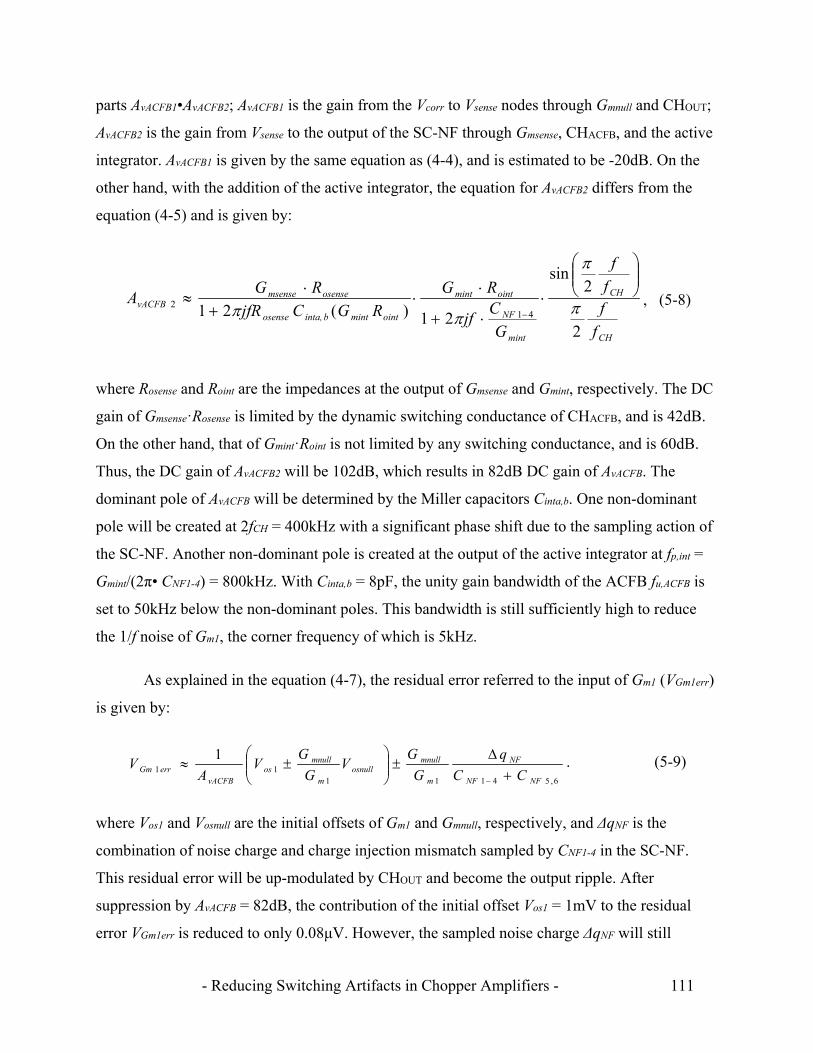
- Reducing Switching Artifacts in Chopper Amplifiers - 111
parts AvACFB1•AvACFB2; AvACFB1 is the gain from the Vcorr to Vsense nodes through Gmnull and CHOUT;
AvACFB2 is the gain from Vsense to the output of the SC-NF through Gmsense, CHACFB, and the active
integrator. AvACFB1 is given by the same equation as (4-4), and is estimated to be -20dB. On the
other hand, with the addition of the active integrator, the equation for AvACFB2 differs from the
equation (4-5) and is given by:
CH
CH
mint
NF
ointmint
ointmintbinta,osense
osensemsensevACFB
f
ff
f
G
Cjf
RG
RGCjfR
RGA
2
2sin
21)(21 412
, (5-8)
where Rosense and Roint are the impedances at the output of Gmsense and Gmint, respectively. The DC
gain of Gmsense·Rosense is limited by the dynamic switching conductance of CHACFB, and is 42dB.
On the other hand, that of Gmint·Roint is not limited by any switching conductance, and is 60dB.
Thus, the DC gain of AvACFB2 will be 102dB, which results in 82dB DC gain of AvACFB. The
dominant pole of AvACFB will be determined by the Miller capacitors Cinta,b. One non-dominant
pole will be created at 2fCH = 400kHz with a significant phase shift due to the sampling action of
the SC-NF. Another non-dominant pole is created at the output of the active integrator at fp,int =
Gmint/(2π• CNF1-4) = 800kHz. With Cinta,b = 8pF, the unity gain bandwidth of the ACFB fu,ACFB is
set to 50kHz below the non-dominant poles. This bandwidth is still sufficiently high to reduce
the 1/f noise of Gm1, the corner frequency of which is 5kHz.
As explained in the equation (4-7), the residual error referred to the input of Gm1 (VGm1err)
is given by:
6,5411111
1
NFNF
NF
m
mnullosnull
m
mnullos
vACFBerrGm CC
q
G
GV
G
GV
AV
. (5-9)
where Vos1 and Vosnull are the initial offsets of Gm1 and Gmnull, respectively, and ΔqNF is the
combination of noise charge and charge injection mismatch sampled by CNF1-4 in the SC-NF.
This residual error will be up-modulated by CHOUT and become the output ripple. After
suppression by AvACFB = 82dB, the contribution of the initial offset Vos1 = 1mV to the residual
error VGm1err is reduced to only 0.08μV. However, the sampled noise charge ΔqNF will still
- Reducing Switching Artifacts in Chopper Amplifiers - 112
dominate the noise PSD peak at the chopping frequency fCH, even though it will be attenuated by
Gmnull/Gm1 = 1/40. This sampled noise is particularly dominated by the thermal noise of Gmint
which is not band-limited by Cinta,b but only by CNF1-4. Moreover, CNF1-4 = 1pF is relatively low
to push fp,int to a higher frequency. In summary, while the newly added Gmint decreases the
residual ripple due to the initial offset of Gm1, it will add to the up-modulated sampled noise.
Overall, this op-amp achieves a 62nV/√Hz maximum noise PSD peak at fCH, which is an
improvement on the 820nV/√Hz achieved in Chapter 4.
5.2.5 High Frequency Path (HFP)
The HFP consists of a feedforward transconductor Gm4 and a current mirror F2. In addition,
output transconductors Gm3, Gm3B, and Gm3CMFB are shared by the LFP and HFP. The unity gain
bandwidth of the HFP fu" is given by:
4 2
2 ,
1
2 2m
um a b
G Ff
C . (5-10)
This must be matched to that of the LFP fu', otherwise a pole-zero doublet and hence phase error
would be introduced into the overall signal transfer function. To achieve this, Gm1 and Gm4
employ the same transconductor topology, and capacitors Cm1a,b and Cm2a,b are laid out
identically. Nevertheless, there will be up to ±2% bandwidth mismatch due to the random
variation in each transconductance and capacitance, which will result in a phase error of up to ±4
degrees. While F2 is unity, Gm4 is set four times smaller than Gm1 to reduce the amount of current
consumed. The noise PSD of Gm4 will be suppressed by the LFP in frequencies lower than fCH.
Since Gm2 and Gm4 are not chopped, their input offsets Vos2 and Vos4 cause a residual offset Vos_res
in conjunction with the finite voltage gain of Gm1 and F1 (Av1):
1
2
442
_v
m
mosos
resos AG
GVV
V
. (5-11)
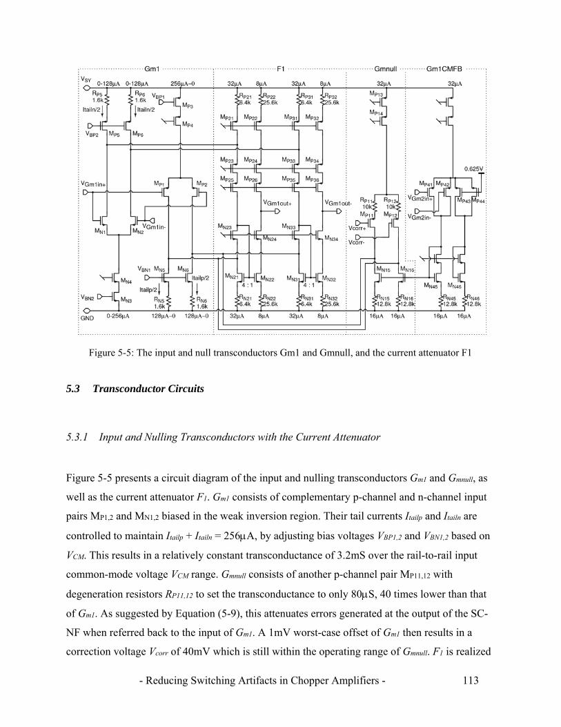
- Reducing Switching Artifacts in Chopper Amplifiers - 113
5.3 Transconductor Circuits
5.3.1 Input and Nulling Transconductors with the Current Attenuator
Figure 5-5 presents a circuit diagram of the input and nulling transconductors Gm1 and Gmnull, as
well as the current attenuator F1. Gm1 consists of complementary p-channel and n-channel input
pairs MP1,2 and MN1,2 biased in the weak inversion region. Their tail currents Itailp and Itailn are
controlled to maintain Itailp + Itailn = 256A, by adjusting bias voltages VBP1,2 and VBN1,2 based on
VCM. This results in a relatively constant transconductance of 3.2mS over the rail-to-rail input
common-mode voltage VCM range. Gmnull consists of another p-channel pair MP11,12 with
degeneration resistors RP11,12 to set the transconductance to only 80S, 40 times lower than that
of Gm1. As suggested by Equation (5-9), this attenuates errors generated at the output of the SC-
NF when referred back to the input of Gm1. A 1mV worst-case offset of Gm1 then results in a
correction voltage Vcorr of 40mV which is still within the operating range of Gmnull. F1 is realized
Figure 5-5: The input and null transconductors Gm1 and Gmnull, and the current attenuator F1
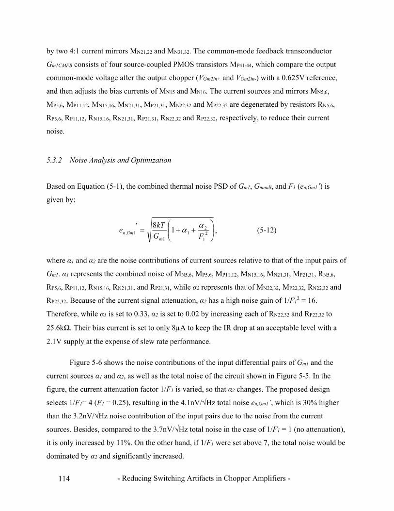
- Reducing Switching Artifacts in Chopper Amplifiers - 114
by two 4:1 current mirrors MN21,22 and MN31,32. The common-mode feedback transconductor
Gm1CMFB consists of four source-coupled PMOS transistors MP41-44, which compare the output
common-mode voltage after the output chopper (VGm2in+ and VGm2in-) with a 0.625V reference,
and then adjusts the bias currents of MN15 and MN16. The current sources and mirrors MN5,6,
MP5,6, MP11,12, MN15,16, MN21,31, MP21,31, MN22,32 and MP22,32 are degenerated by resistors RN5,6,
RP5,6, RP11,12, RN15,16, RN21,31, RP21,31, RN22,32 and RP22,32, respectively, to reduce their current
noise.
5.3.2 Noise Analysis and Optimization
Based on Equation (5-1), the combined thermal noise PSD of Gm1, Gmnull, and F1 (en,Gm1’) is
given by:
2
1
21
11, 1
8
FG
kTe
mGmn
, (5-12)
where α1 and α2 are the noise contributions of current sources relative to that of the input pairs of
Gm1. α1 represents the combined noise of MN5,6, MP5,6, MP11,12, MN15,16, MN21,31, MP21,31, RN5,6,
RP5,6, RP11,12, RN15,16, RN21,31, and RP21,31, while α2 represents that of MN22,32, MP22,32, RN22,32 and
RP22,32. Because of the current signal attenuation, α2 has a high noise gain of 1/F12 = 16.
Therefore, while α1 is set to 0.33, α2 is set to 0.02 by increasing each of RN22,32 and RP22,32 to
25.6kΩ. Their bias current is set to only 8A to keep the IR drop at an acceptable level with a
2.1V supply at the expense of slew rate performance.
Figure 5-6 shows the noise contributions of the input differential pairs of Gm1 and the
current sources α1 and α2, as well as the total noise of the circuit shown in Figure 5-5. In the
figure, the current attenuation factor 1/F1 is varied, so that α2 changes. The proposed design
selects 1/F1= 4 (F1 = 0.25), resulting in the 4.1nV/√Hz total noise en,Gm1’, which is 30% higher
than the 3.2nV/√Hz noise contribution of the input pairs due to the noise from the current
sources. Besides, compared to the 3.7nV/√Hz total noise in the case of 1/F1 = 1 (no attenuation),
it is only increased by 11%. On the other hand, if 1/F1 were set above 7, the total noise would be
dominated by α2 and significantly increased.

- Reducing Switching Artifacts in Chopper Amplifiers - 115
To evaluate the effectiveness of the proposed frequency compensation techniques, the
design parameters used in Figure 5-2 are listed in Table 5-1, and are compared with those in
Figure 5-1. Their noise PSDs are set to the same 4.1nV/√Hz (excluding the contribution from the
input chopper), so that the required transconductance of Gm1 is larger in Figure 5-2 to
compensate for the extra noise contribution of F1. Two design cases are considered in Figure 5-1
to maintain the stability of the overall op-amp: increasing the transconductances hence the
Figure 5-6: Noise contributions of the current sources versus current attenuation
Table 5-1: Design parameter comparison between Figures 5-1 and 5-2
- Reducing Switching Artifacts in Chopper Amplifiers - 116
currents of Gm2 and Gm3 while maintaining the same total capacitor value as Figure 5-2; or
increasing the capacitor size while maintaining the total current same as Figure 5-2. While one
case in Figure 5-1 consumes 2798µA of current, the case in Figure 5-2 only consumes 1040µA.
While the other case in Figure 5-1 requires 162pF of total capacitor, the case in Figure 5-2 only
requires 64pF. However, the slew rate of the proposed circuit in Figure 5-2 is 5.6 times less than
the case of increasing the capacitor size in Figure 5-1.
5.3.3 Residual Offset and CMRR Analysis
The degeneration resistors RN22,23 and RP22,23 also increase the output impedance of F1
with series feedback. As a result, the combined DC gain of Gm1 and F1 (Av1) is mainly limited by
the dynamic output conductance due to the output chopping [4], and thus is given by:
dB864 1
111
OUTFchop
mv Cf
FGA , (5-13)
where COUTF1 = 50fF is the combined drain capacitance of the cascode devices MN24, MN34, MP26,
and MP36. This gain is sufficiently high to reduce the offset contribution of Gm2 and Gm4. Based
on Equation (5-11), their worst-case offsets Vos2 = Vos4 = 2mV together will contribute to the
overall offset only by 0.14V. With the change in the input common-mode voltage, the gain Av1
and Vos2 will be mostly constant, but Vos4 will change due to the offset mismatch between the two
complementary input pairs. When Vos4 changes from –2mV to +2mV with the 2.1V input
common-mode voltage change, the residual offset changes from –0.1V to +0.1V,
corresponding to the 140dB CMRR.
As discussed in Section 5.2.2, F1 should not generate common-mode output current to
avoid affecting the output common-mode voltage VoutCM. This is achieved by setting the output
source and sink currents to an equal amount during a large signal response. The maximum output
source current is 8A, which is generated by the PMOS current sources MP22 and MP23. The gate
of the NMOS cascode devices MN24,34 is biased such that the maximum output sink current is
limited to the same 8A.

- Reducing Switching Artifacts in Chopper Amplifiers - 117
5.3.4 Second and Output Transconductors
The feedforward transconductor Gm4 and the current mirror F2 use the same topologies as Gm1
and F1, to improve the matching of the bandwidth between the LFP and HFP. Figure 5-7 presents
a circuit diagram of the second and output stage transconductors Gm2, Gm3, and Gm3B. Gm2
consists of a p-channel input pair MP21,22 and the output currents IGm2+ and IGm2- are combined
with those of F2 (IF2+ and IF2-). One of the combined currents IGm3+ then drives high and low side
voltages VGm3P and VGm3N in a mesh folded stage [16]. These voltages control high and low side
transistors MN31,P31 to form a class-AB output transconductor Gm3. The quiescent current is set to
256A by local feedback. Based on one of the replica output currents In32 or Ip32, whichever is
lower, a minimum selector circuit generates a voltage VFB to adjust the difference of VGm3P and
VGm3N. This topology can operate below a 2.1V supply, since it only requires one gate-source
voltage plus two drain-source voltages between the supply rails. Two 8pF frequency
compensation capacitors Cm2aP,N together represent Cm2a in Figure 5-3. The dummy output
transconductor Gm3B consists of the same topology as Gm3, but the size and bias currents of every
transistor are scaled to one-fourth of those in Gm3. When driving a 2kΩ load, Gm3 can swing
close to each supply rail with 100mV of headroom, while providing a 10dB gain. Combined with
the 86 and 40dB gains of Gm1 and Gm2, respectively, the overall op-amp achieves an open-loop
gain of 136dB.
Figure 5-7: The second and output stage transconductors Gm2, Gm3, and Gm3B
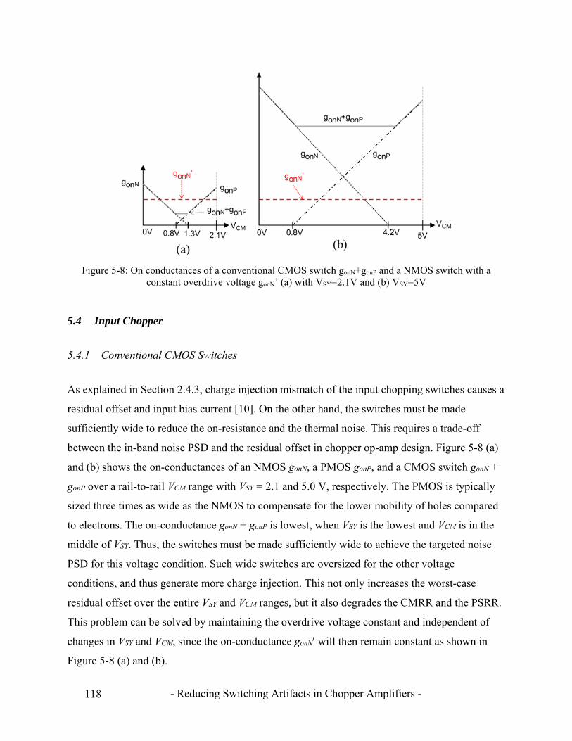
- Reducing Switching Artifacts in Chopper Amplifiers - 118
5.4 Input Chopper
5.4.1 Conventional CMOS Switches
As explained in Section 2.4.3, charge injection mismatch of the input chopping switches causes a
residual offset and input bias current [10]. On the other hand, the switches must be made
sufficiently wide to reduce the on-resistance and the thermal noise. This requires a trade-off
between the in-band noise PSD and the residual offset in chopper op-amp design. Figure 5-8 (a)
and (b) shows the on-conductances of an NMOS gonN, a PMOS gonP, and a CMOS switch gonN +
gonP over a rail-to-rail VCM range with VSY = 2.1 and 5.0 V, respectively. The PMOS is typically
sized three times as wide as the NMOS to compensate for the lower mobility of holes compared
to electrons. The on-conductance gonN + gonP is lowest, when VSY is the lowest and VCM is in the
middle of VSY. Thus, the switches must be made sufficiently wide to achieve the targeted noise
PSD for this voltage condition. Such wide switches are oversized for the other voltage
conditions, and thus generate more charge injection. This not only increases the worst-case
residual offset over the entire VSY and VCM ranges, but it also degrades the CMRR and the PSRR.
This problem can be solved by maintaining the overdrive voltage constant and independent of
changes in VSY and VCM, since the on-conductance gonN' will then remain constant as shown in
Figure 5-8 (a) and (b).
Figure 5-8: On conductances of a conventional CMOS switch gonN+gonP and a NMOS switch with a constant overdrive voltage gonN’ (a) with VSY=2.1V and (b) VSY=5V
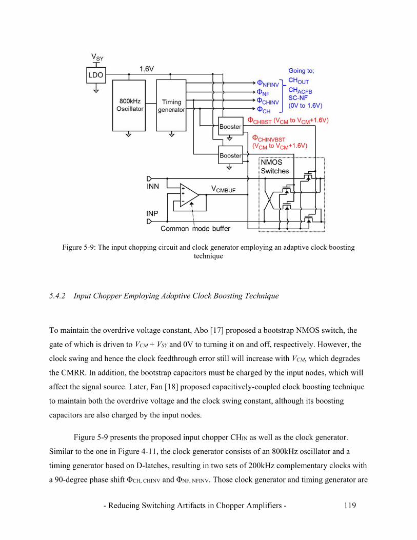
- Reducing Switching Artifacts in Chopper Amplifiers - 119
5.4.2 Input Chopper Employing Adaptive Clock Boosting Technique
To maintain the overdrive voltage constant, Abo [17] proposed a bootstrap NMOS switch, the
gate of which is driven to VCM + VSY and 0V to turning it on and off, respectively. However, the
clock swing and hence the clock feedthrough error still will increase with VCM, which degrades
the CMRR. In addition, the bootstrap capacitors must be charged by the input nodes, which will
affect the signal source. Later, Fan [18] proposed capacitively-coupled clock boosting technique
to maintain both the overdrive voltage and the clock swing constant, although its boosting
capacitors are also charged by the input nodes.
Figure 5-9 presents the proposed input chopper CHIN as well as the clock generator.
Similar to the one in Figure 4-11, the clock generator consists of an 800kHz oscillator and a
timing generator based on D-latches, resulting in two sets of 200kHz complementary clocks with
a 90-degree phase shift ΦCH, CHINV and ΦNF, NFINV. Those clock generator and timing generator are
Figure 5-9: The input chopping circuit and clock generator employing an adaptive clock boosting technique
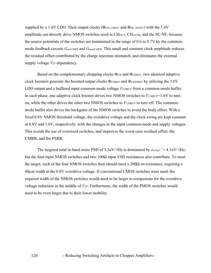
- Reducing Switching Artifacts in Chopper Amplifiers - 120
supplied by a 1.6V LDO. Their output clocks (ΦCH, CHINV and ΦNF, NFINV) with the 1.6V
amplitude can directly drive NMOS switches used in CHOUT, CHACFB, and the SC-NF, because
the source potentials of the switches are maintained in the range of 0.6 to 0.7V by the common-
mode feedback circuits Gm1CMFB and GmintCMFB. This small and constant clock amplitude reduces
the residual offset contributed by the charge injection mismatch, and eliminates the external
supply voltage VSY dependency.
Based on the complementary chopping clocks ΦCH and ΦCHINV, two identical adaptive
clock boosters generate the boosted output clocks ΦCHBST and ΦCHINBST by utilizing the 1.6V
LDO output and a buffered input common-mode voltage VCMBUF from a common-mode buffer.
In each phase, one adaptive clock booster drives two NMOS switches to VCMBUF+1.6V to turn
on, while the other drives the other two NMOS switches to VCMBUF to turn off. The common-
mode buffer also drives the backgates of the NMOS switches to avoid the body effect. With a
fixed 0.8V NMOS threshold voltage, the overdrive voltage and the clock swing are kept constant
at 0.8V and 1.6V, respectively, with the changes in the input common-mode and supply voltages.
This avoids the use of oversized switches, and improves the worst-case residual offset, the
CMRR, and the PSRR.
The targeted total in-band noise PSD of 5.2nV/√Hz is dominated by en,Gm1’ = 4.1nV/√Hz,
but the four input NMOS switches and two 100Ω input ESD resistances also contribute. To meet
the target, each of the four NMOS switches then should meet a 200Ω on-resistance, requiring a
48m width at the 0.8V overdrive voltage. If conventional CMOS switches were used, the
required width of the NMOS switches would need to be larger to compensate for the overdrive
voltage reduction in the middle of VSY. Furthermore, the width of the PMOS switches would
need to be even larger due to their lower mobility.
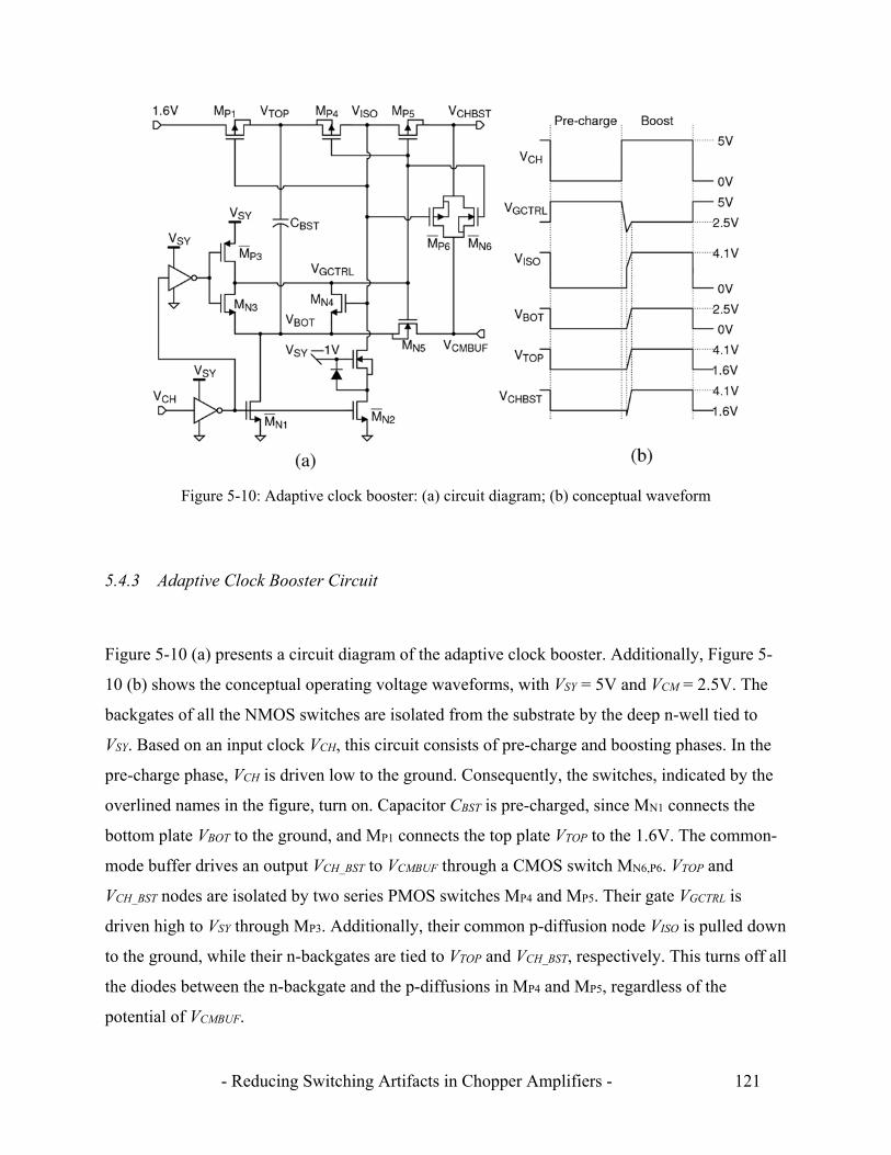
- Reducing Switching Artifacts in Chopper Amplifiers - 121
5.4.3 Adaptive Clock Booster Circuit
Figure 5-10 (a) presents a circuit diagram of the adaptive clock booster. Additionally, Figure 5-
10 (b) shows the conceptual operating voltage waveforms, with VSY = 5V and VCM = 2.5V. The
backgates of all the NMOS switches are isolated from the substrate by the deep n-well tied to
VSY. Based on an input clock VCH, this circuit consists of pre-charge and boosting phases. In the
pre-charge phase, VCH is driven low to the ground. Consequently, the switches, indicated by the
overlined names in the figure, turn on. Capacitor CBST is pre-charged, since MN1 connects the
bottom plate VBOT to the ground, and MP1 connects the top plate VTOP to the 1.6V. The common-
mode buffer drives an output VCH_BST to VCMBUF through a CMOS switch MN6,P6. VTOP and
VCH_BST nodes are isolated by two series PMOS switches MP4 and MP5. Their gate VGCTRL is
driven high to VSY through MP3. Additionally, their common p-diffusion node VISO is pulled down
to the ground, while their n-backgates are tied to VTOP and VCH_BST, respectively. This turns off all
the diodes between the n-backgate and the p-diffusions in MP4 and MP5, regardless of the
potential of VCMBUF.
Figure 5-10: Adaptive clock booster: (a) circuit diagram; (b) conceptual waveform
- Reducing Switching Artifacts in Chopper Amplifiers - 122
In the boosting phase, VCH is driven high to VSY. Consequently, the switches, indicated by
the names not overlined in the figure, turn on. First, VBOT and VISO become disconnected from the
ground. VGCTRL goes down toward VBOT due to the discharge through MN3. When VGCTRL reaches
below 0.8V, MP4 and MP5 turn on, connecting VTOP, VISO, and VCH_BST to the 1.6V together. VISO
then turns MP1 off to disconnect VTOP from the 1.6V. Additionally, VISO turns MN5 on, so that
VBOT climbs to VCMBUF, which is driven by the common-mode buffer. This boosts VTOP, VISO, and
VCH_BST up to VCMBUF+1.6V through the pre-charged capacitor CBST.
Note that when VSY and VCM are 5V, VCH_BST will be 6.6V in the boosting phase. However,
every single transistor has relative terminal voltages less than 5V, to ensure reliability. The gate-
source voltages of MP4 and MP5 are kept at –1.6V by VGCTRL = VCMBUF, and that of MN5 is kept at
1.6V by VISO = VCMBUF+1.6V. Additionally, the drain-source voltage of MN2 is kept less than 5V
by an NMOS cascode and a clamp diode.
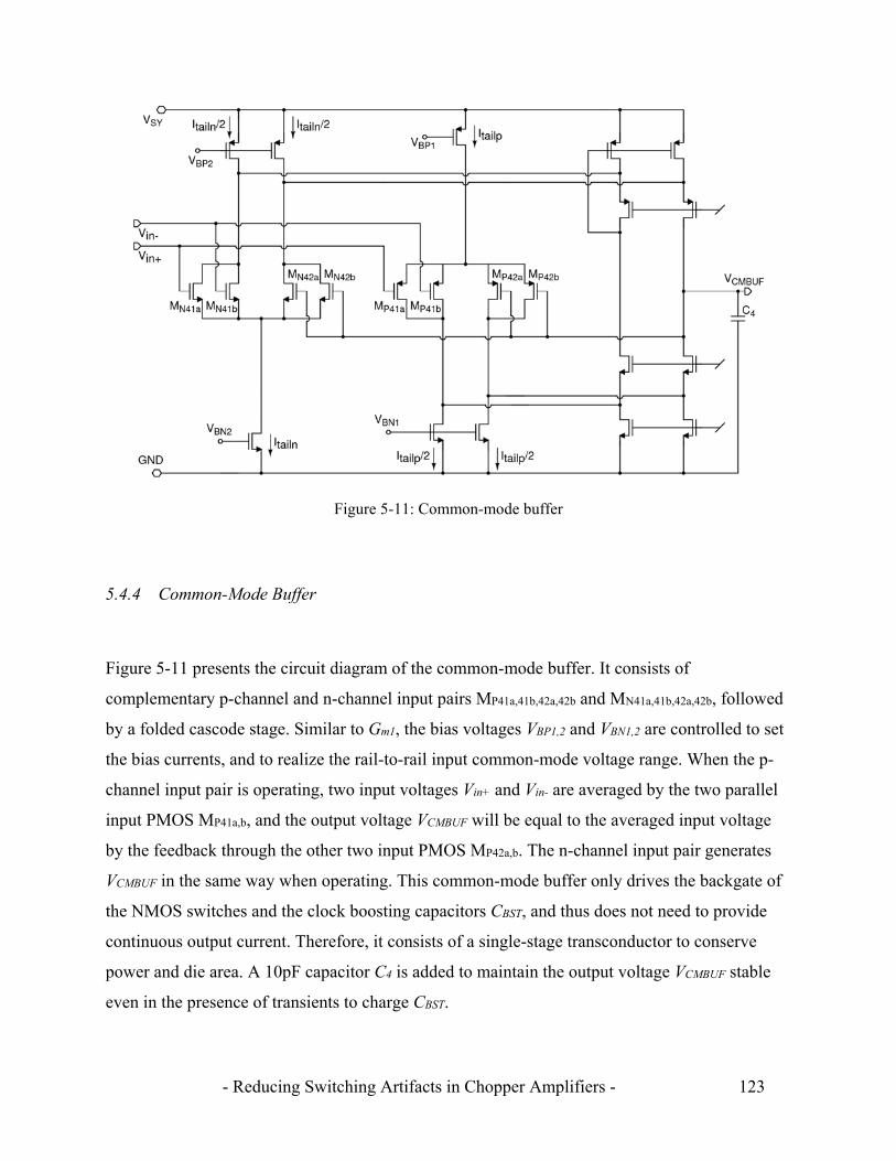
- Reducing Switching Artifacts in Chopper Amplifiers - 123
5.4.4 Common-Mode Buffer
Figure 5-11 presents the circuit diagram of the common-mode buffer. It consists of
complementary p-channel and n-channel input pairs MP41a,41b,42a,42b and MN41a,41b,42a,42b, followed
by a folded cascode stage. Similar to Gm1, the bias voltages VBP1,2 and VBN1,2 are controlled to set
the bias currents, and to realize the rail-to-rail input common-mode voltage range. When the p-
channel input pair is operating, two input voltages Vin+ and Vin- are averaged by the two parallel
input PMOS MP41a,b, and the output voltage VCMBUF will be equal to the averaged input voltage
by the feedback through the other two input PMOS MP42a,b. The n-channel input pair generates
VCMBUF in the same way when operating. This common-mode buffer only drives the backgate of
the NMOS switches and the clock boosting capacitors CBST, and thus does not need to provide
continuous output current. Therefore, it consists of a single-stage transconductor to conserve
power and die area. A 10pF capacitor C4 is added to maintain the output voltage VCMBUF stable
even in the presence of transients to charge CBST.
Figure 5-11: Common-mode buffer
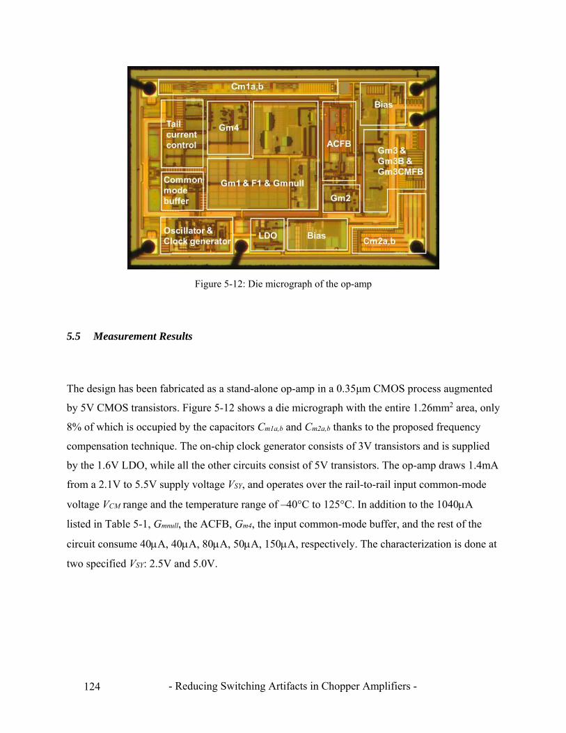
- Reducing Switching Artifacts in Chopper Amplifiers - 124
5.5 Measurement Results
The design has been fabricated as a stand-alone op-amp in a 0.35μm CMOS process augmented
by 5V CMOS transistors. Figure 5-12 shows a die micrograph with the entire 1.26mm2 area, only
8% of which is occupied by the capacitors Cm1a,b and Cm2a,b thanks to the proposed frequency
compensation technique. The on-chip clock generator consists of 3V transistors and is supplied
by the 1.6V LDO, while all the other circuits consist of 5V transistors. The op-amp draws 1.4mA
from a 2.1V to 5.5V supply voltage VSY, and operates over the rail-to-rail input common-mode
voltage VCM range and the temperature range of –40°C to 125°C. In addition to the 1040A
listed in Table 5-1, Gmnull, the ACFB, Gm4, the input common-mode buffer, and the rest of the
circuit consume 40A, 40A, 80A, 50A, 150A, respectively. The characterization is done at
two specified VSY: 2.5V and 5.0V.
Figure 5-12: Die micrograph of the op-amp
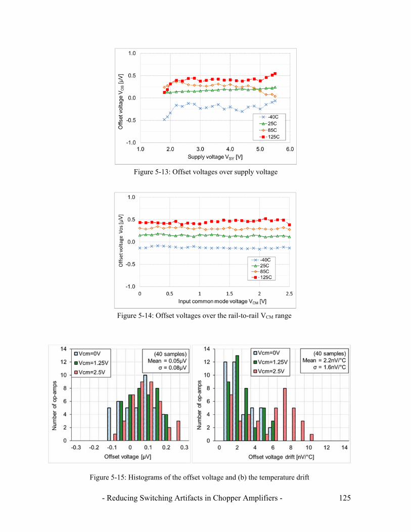
- Reducing Switching Artifacts in Chopper Amplifiers - 125
Figure 5-13: Offset voltages over supply voltage
Figure 5-14: Offset voltages over the rail-to-rail VCM range
Figure 5-15: Histograms of the offset voltage and (b) the temperature drift
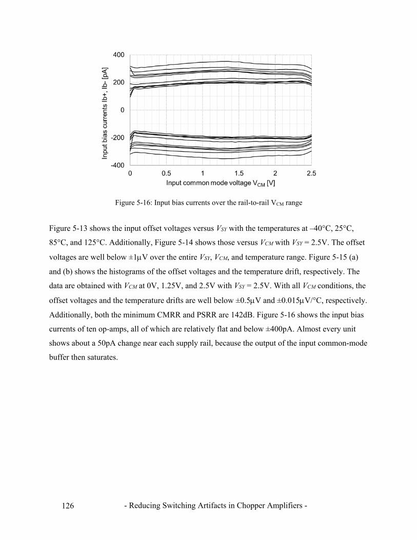
- Reducing Switching Artifacts in Chopper Amplifiers - 126
Figure 5-13 shows the input offset voltages versus VSY with the temperatures at –40°C, 25°C,
85°C, and 125°C. Additionally, Figure 5-14 shows those versus VCM with VSY = 2.5V. The offset
voltages are well below ±1V over the entire VSY, VCM, and temperature range. Figure 5-15 (a)
and (b) shows the histograms of the offset voltages and the temperature drift, respectively. The
data are obtained with VCM at 0V, 1.25V, and 2.5V with VSY = 2.5V. With all VCM conditions, the
offset voltages and the temperature drifts are well below ±0.5V and ±0.015V/°C, respectively.
Additionally, both the minimum CMRR and PSRR are 142dB. Figure 5-16 shows the input bias
currents of ten op-amps, all of which are relatively flat and below ±400pA. Almost every unit
shows about a 50pA change near each supply rail, because the output of the input common-mode
buffer then saturates.
Figure 5-16: Input bias currents over the rail-to-rail VCM range
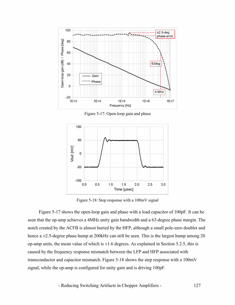
- Reducing Switching Artifacts in Chopper Amplifiers - 127
Figure 5-17 shows the open-loop gain and phase with a load capacitor of 100pF. It can be
seen that the op-amp achieves a 4MHz unity gain bandwidth and a 63-degree phase margin. The
notch created by the ACFB is almost buried by the HFP, although a small pole-zero doublet and
hence a ±2.5-degree phase hump at 200kHz can still be seen. This is the largest hump among 20
op-amp units, the mean value of which is ±1.6 degrees. As explained in Section 5.2.5, this is
caused by the frequency response mismatch between the LFP and HFP associated with
transconductor and capacitor mismatch. Figure 5-18 shows the step response with a 100mV
signal, while the op-amp is configured for unity gain and is driving 100pF.
Figure 5-17: Open-loop gain and phase
Figure 5-18: Step response with a 100mV signal

- Reducing Switching Artifacts in Chopper Amplifiers - 128
Figure 5-19 shows the total harmonic distortion (THD) versus input signal amplitude with
1kHz and 10kHz signals, unity gain configuration, and VSY=5V. The result indicates that the total
error is dominated by the distortion when the signal amplitude increases above 1Vrms. Figure 5-
20 also shows the THD over input signal frequency with a 1Vp-p signal amplitude and VCM = 1, 2,
3, and 4V. In the higher frequencies above 1kHz, the THD is worse with VCM = 4V by 20dB.
This is because, when the input common-mode voltage crosses over 3.8V, the operation of the
input stage Gm1 transitions between p-channel and n-channel pairs, each of which has unique
initial offset. After this transition occurs, the ACFB has to be settled to a different value of initial
offset, during which residual ripple is generated. This residual ripple occurs twice every input
signal period, which causes extra distortion.
Figure 5-19: THD versus signal amplitude
Figure 5-20 THD over the frequency with VCM = 1V, 2V, 3V, 4V
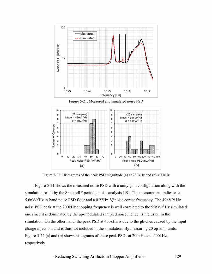
- Reducing Switching Artifacts in Chopper Amplifiers - 129
Figure 5-21 shows the measured noise PSD with a unity gain configuration along with the
simulation result by the SpectreRF periodic noise analysis [19]. The measurement indicates a
5.6nV/√Hz in-band noise PSD floor and a 0.22Hz 1/f noise corner frequency. The 49nV/√ Hz
noise PSD peak at the 200kHz chopping frequency is well correlated to the 55nV/√ Hz simulated
one since it is dominated by the up-modulated sampled noise, hence its inclusion in the
simulation. On the other hand, the peak PSD at 400kHz is due to the glitches caused by the input
charge injection, and is thus not included in the simulation. By measuring 20 op-amp units,
Figure 5-22 (a) and (b) shows histograms of these peak PSDs at 200kHz and 400kHz,
respectively.
Figure 5-21: Measured and simulated noise PSD
Figure 5-22: Histograms of the peak PSD magnitude (a) at 200kHz and (b) 400kHz

- Reducing Switching Artifacts in Chopper Amplifiers - 130
Lastly, the specified performance is summarized in Table 5-2, and is compared with the
other state-of-the-art chopper op-amps operating below a 5V supply. The listed numbers are
obtained at the specified supply voltage (VSY) of each op-amp. The proposed op-amp is specified
with the lowest supply voltage of 2.5V and offers a rail-to-rail input range. It also achieves the
lowest maximum offset voltage of 0.5V, the lowest noise PSD of 5.6nV/√Hz, and a high
minimum CMRR of 142dB.
5.6 Conclusion
A 5.6nV/√Hz chopper op-amp has been realized by employing frequency compensation
technique using the current attenuator and the dummy differential output. This technique relaxes
the trade-off between in-band noise PSD, current consumption, and capacitor size, so that the op-
amp only draws 1.4mA from a 2.1V to 5.5V supply and occupies a die area of 1.26mm2. It also
achieves a 4MHz unity gain bandwidth while driving a load capacitor of up to 100pF. Moreover,
ACFB is used to suppress the up-modulated ripple, and the resulting notch at the 200kHz
Table 5-2: Comparison with other state-of-the-art
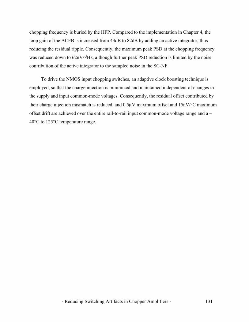
- Reducing Switching Artifacts in Chopper Amplifiers - 131
chopping frequency is buried by the HFP. Compared to the implementation in Chapter 4, the
loop gain of the ACFB is increased from 43dB to 82dB by adding an active integrator, thus
reducing the residual ripple. Consequently, the maximum peak PSD at the chopping frequency
was reduced down to 62nV/√Hz, although further peak PSD reduction is limited by the noise
contribution of the active integrator to the sampled noise in the SC-NF.
To drive the NMOS input chopping switches, an adaptive clock boosting technique is
employed, so that the charge injection is minimized and maintained independent of changes in
the supply and input common-mode voltages. Consequently, the residual offset contributed by
their charge injection mismatch is reduced, and 0.5V maximum offset and 15nV/°C maximum
offset drift are achieved over the entire rail-to-rail input common-mode voltage range and a –
40°C to 125°C temperature range.
- Reducing Switching Artifacts in Chopper Amplifiers - 132
5.7 References
[1] W. Kester, J. Bryant, and W. Jung, “Amplifiers for signal conditioning, Section 3”, 1999,
Accessed on March 2018, [Online] Available: <http://www.analog.com/media/en/training-
seminars/design-handbooks/sensor-signal-cond-sect3.PDF>.
[2] Analog Devices, “CN-0181: Precision, 16-Bit, Voltage Level Setting with Less than 5 mW
Total Power Dissipation”, Mar. 2011, Accessed on March 2018, [Online] Available:
<http://www.analog.com/media/en/reference-design-documentation/reference-
designs/CN0181.pdf>.
[3] C. C. Enz and G. C. Temes, “Circuit Techniques for Reducing the Effect of Op-Amp
Imperfections: Autozeroing, Correlated Double Sampling, and Chopper Stabilization”, Proc. of
IEEE, vol. 84, no. 9, pp. 1320-1324, Sept. 1996.
[4] J. F. Witte, K. A. A. Makinwa, and J. H. Huijsing, Dynamic Offset Compensated CMOS
Amplifiers. New York: Springer, 2010
[5] A. T. K. Tang, “A 3V-Offset Operational Amplifier with 20nV/√Hz Input Noise PSD at DC
Employing both Chopping and Autozeroing”, IEEE ISSCC Dig. Tech. Papers, pp. 362-387, Feb.
2002.
[6] Intersil Corporation, “ISL28134 Datasheet”, June 2011, Accessed on March 2018, [Online]
Available: <http://www.intersil.com/content/dam/Intersil/documents/isl2/isl28134.pdf>.
[7] Texas Instruments, “LMP2021 Datasheet”, Sept. 2009, Accessed on March 2018, [Online]
Available: <http://www.ti.com/lit/ds/symlink/lmp2022.pdf>.
[8] R. Burt and J. Zhang, “A Micropower Chopper-Stabilized Operational Amplifier using a SC
Notch Filter with Synchronous Integration inside the Continuous-Time Signal Path”, IEEE J.
Solid-State Circuits, vol. 41, no. 12, pp. 2729-2736, Dec. 2006.
[9] M. Belloni, E. Bonizzoni, A. Fornasari, and F. Maloberti, “A Micropower Chopper-CDS
Operational Amplifier”, IEEE J. Solid-State Circuits, vol. 45, no. 12, pp. 2521-2529, Dec. 2010.
- Reducing Switching Artifacts in Chopper Amplifiers - 133
[10] Q. Fan, J. H. Huijsing, and K.A.A. Makinwa, “A 21 nV/√Hz Chopper-Stabilized Multi-Path
Current-Feedback Instrumentation Amplifier With 2 µV Offset”, IEEE J. Solid-State Circuits,
vol. 47, no. 2, pp. 464-475, Feb. 2012.
[11] Y. Kusuda, “Auto Correction Feedback for Ripple Suppression in a Chopper Amplifier”,
IEEE J. Solid-State Circuits, vol. 45, no. 8, pp. 1436-1445, Aug. 2010.
[12] M. Kejariwal, P. Ammisetti, and A. Thomsen, “A 250+dB open loop gain feedforward
compensated high precision operational amplifier”, Proc. of IEEE ESSCIRC, pp. 187-190, Sept.
2002.
[13] Cirrus Logic, “CS3002 Datasheet”, Oct. 2004, Accessed on March 2018, [Online]
Available: <http://www.cirrus.com/cn/pubs/proDatasheet/CS3002_F10.pdf>.
[14] Maxim Integrated, “MAX44250 Datasheet”, Oct. 2011, Accessed on March 2018, [Online]
Available: <http://datasheets.maximintegrated.com/en/ds/MAX44250-MAX44252.pdf>.
[15] R. G. H. Eschauzier, L. P. T. Kerklaan, and J. H. Huijsing, “A 100-MHz 100-dB
Operational Amplifier with Multipath Nested Miller Compensation Structure”, IEEE J. Solid-
State Circuits, vol. 27, no. 12, pp. 1709-1717, Dec. 1992.
[16] K-J. Langen and J. H. Huijsing, “Compact Low-Voltage Power-Efficient Operational
Amplifier Cells for VLSI”, IEEE J. Solid-State Circuits, vol. 33, no. 10, pp. 1482-1496, Oct.
1998.
[17] A. M. Abo and P. R. Gray, “A 1.5-V, 10-bit, 14.3-MS/s CMOS pipeline analog-to-digital
converter”, IEEE J. Solid-State Circuits, vol. 34, no. 5, pp. 599-606, May 1999.
[18] Q. Fan, J. Huijsing, and K. Makinwa, “A Capacitively Coupled Chopper Instrumentation
Amplifier with a ±30V Common-Mode Range, 160dB CMRR and 5V Offset”, IEEE ISSCC
Dig. Tech. Papers, pp. 374-375, Feb. 2012.
[19] K. Kundert, “Simulating Switched-Capacitor Filters with SpectreRF”, July 2006, Accessed
on March 2018, [Online] Available: <http://www.designers-guide.org/Analysis/sc-filters.pdf>.
- Reducing Switching Artifacts in Chopper Amplifiers - 134

- Reducing Switching Artifacts in Chopper Amplifiers - 135
Chapter 6
Auto-Zero and Chopper Op-Amp with Clock Interleaving and
Input Bias Current Trimming Techniques3
This chapter presents an auto-zero and chopper operational amplifier that operates from a 4.5V
to 60V supply and is realized in a 0.18m CMOS process augmented by 5V CMOS and 60V
DMOS transistors [1]. It achieves a 0.02V/°C maximum offset voltage drift, a 145dB minimum
CMRR, a 5.8nV/√Hz noise PSD, and a 3.1MHz unity gain bandwidth, while consuming 840A
of current.
First, Section 6.1 describes the motivation for reducing the ripple and glitch errors for
wide bandwidth applications, as well as the associated technical challenges. In Section 6.2, a
capacitively-coupled auto-zeroed and chopped input transconductor is proposed consisting of six
parallel channels, each of which is driven by interleaved 800kHz clocks. While the auto-zeroing
reduces the initial offset and therefore the up-modulated ripple, the interleaving technique pushes
the majority of the glitch energy up to 4.8MHz. Section 6.3 proposes an on-chip charge
mismatch compensation circuit to reduce the maximum input bias current from 1.5nA to 150pA
at a post-production test. The overall op-amp design is described in Section 6.4, and the
measurement results are discussed in Section 6.5. The chapter ends with a conclusion in Section
6.6.
______________________
3 This chapter is derived from a journal publication of the author: Y. Kusuda, “A 60 V Auto-Zero and Chopper
Operational Amplifier With 800 kHz Interleaved Clocks and Input Bias Current Trimming”, IEEE J. Solid-State
Circuits, vol. 50, no. 12, pp. 2804-2813, Dec. 2015.
- Reducing Switching Artifacts in Chopper Amplifiers - 136
6.1 Motivation
As explained in Section 1.5.3, industrial applications require precision amplifiers with supply
operation above 30V, a wide input common-mode range, and a wide signal bandwidth [2-4].
Most precision amplifiers are realized using Bipolar or JFET processes, to achieve 1V/°C
maximum offset voltage drifts, 10nV/√Hz in-band noise PSDs, and 2MHz unity gain
bandwidths. Recently, op-amps with similar specifications have been reported using CMOS-
based processes with the addition of high voltage DMOS transistors [5-8]. They utilize auto-
zeroing and/or chopping techniques to reduce the high offset voltage drift and 1/f noise
associated with CMOS input transconductors [9]. Such op-amps can be manufactured at a lower
cost, and can achieve lower offset voltage drift and 1/f noise than Bipolar and JFET op-amps.
As explained in Section 2.4, chopping generates up-modulated ripple and glitches,
resulting in peak PSDs at the chopping frequency fCH and its harmonics. Such noise PSD peaks
usually need to be attenuated by low-pass filters, which limits the usable signal bandwidth well
below fCH. On the other hand, a higher chopping frequency will increase the charge injection per
unit of time, and thus degrade the DC specifications such as the offset drift and input bias current
[10]. The charge injection also increases when wider input switches are used for lower on-
resistance and hence, lower thermal noise. A 0.02V/°C maximum offset drift, a 600pA
maximum input bias current, and a 9nV/√Hz voltage noise PSD have been achieved [7],
although the 60kHz chopping frequency limits the usable signal bandwidth. In [5], a higher
chopping frequency of 333kHz is used, resulting in a somewhat worse DC performance: a
0.085V/°C maximum offset drift, an 850pA maximum input bias current, and an 8.8nV/√Hz
voltage noise PSD.
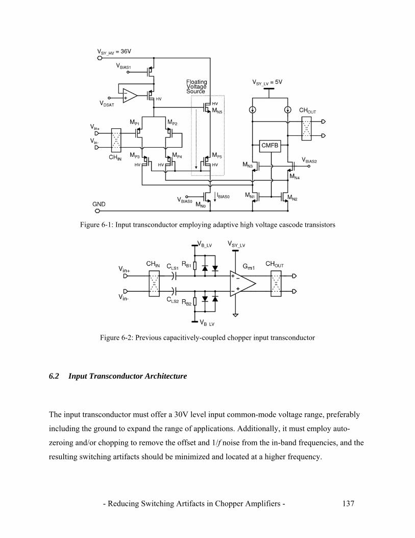
- Reducing Switching Artifacts in Chopper Amplifiers - 137
6.2 Input Transconductor Architecture
The input transconductor must offer a 30V level input common-mode voltage range, preferably
including the ground to expand the range of applications. Additionally, it must employ auto-
zeroing and/or chopping to remove the offset and 1/f noise from the in-band frequencies, and the
resulting switching artifacts should be minimized and located at a higher frequency.
Figure 6-1: Input transconductor employing adaptive high voltage cascode transistors
Figure 6-2: Previous capacitively-coupled chopper input transconductor
- Reducing Switching Artifacts in Chopper Amplifiers - 138
6.2.1 Previous High Voltage Input Transconductors
Figure 6-1 is a chopper input transconductor that offers a 30V level input common-mode voltage
VCM range [3]. The input pair MP1,2 consists of low voltage transistors that have lower offset and
noise than high voltage (HV) transistors for a given device size. The drain-source voltages are
kept lower than the breakdown voltages with adaptive HV cascode transistors MP3,4 and a
floating voltage source. However, this transconductor will probably not perform well with the
input voltages near the ground, since MP3,4 will decrease the voltage headroom of MP1,2.
Moreover, it will consume relatively high power due to a high supply voltage VSY_HV, which
might degrade the performance due to the heat generated near the input pair.
An alternative topology is shown in Figure 6-2, namely the capacitively-coupled chopper
input transconductor proposed by Fan [6,11,12]. Two level shift capacitors CLS1,2 block the DC
input common-mode voltage VCM, while the inputs of a transconductor Gm1 are biased at a fixed
low voltage VB_LV through bias resistors RB1,2. In this case, Gm1 can be supplied by a low supply
voltage VSY_LV and consist of low voltage transistors. DC differential input signals Vin are up-
modulated to the chopping frequency fCH, and then become AC-coupled to Gm1. On the other
hand, AC differential input signals near fCH are down-modulated to DC and then blocked by
CLS1,2, resulting in a notch at fCH. A HFP can be added to bypass the notch, although it still
creates a pole-zero doublet due to the mismatch between the two signal paths. Moreover, RB1,2
needs to be greater than 100MΩ to sufficiently reduce the thermal noise contribution, resulting in
slow settling after a large input common-mode voltage step. Therefore, this topology is less
preferred for applications, where the amplifier’s output must quickly settle with large step input
signals.
Various other approaches to realize a wide input common-mode voltage range are
introduced in [12].

- Reducing Switching Artifacts in Chopper Amplifiers - 139
6.2.2 Capacitively-Coupled Auto-Zero and Chopper Input Transconductor
Figure 6-3 (a) presents the proposed capacitively-coupled auto-zero and chopper input
transconductor, along with the timing diagram in Figure 6-3 (b). During a pre-charge PC phase,
two level shift capacitors CLS1,2 are charged by a non-inverting input voltage Vin+ and a 1.6V
common-mode buffer CM-buf. The input voltages of an input transconductor Gm1 are then biased
at 1.6V and left floating in the subsequent auto-zero AZ, chopping CH, and inverting-chop
CHINV phases. In the AZ phase, the charge injection mismatch sampled by CLS1,2 are cancelled
along with the input offset of Gm1, by forming local feedback with an auto-zeroed transconductor
GmAZ. At the end of the AZ phase, the resulting correction voltage Vcorr is sampled by two auto-
zero capacitors CAZ1,2. In the subsequent CH and CHINV phases, the differential inputs and
outputs of Gm1 are connected to the signal path, amplifying the input signal Vin, while being
chopped. The two CLS1,2 work as floating voltage sources after the PC phase, and thus transfer
the input signals to Gm1 without creating a notch. Moreover, the auto-zeroing reduces the offset
and consequently the ripple, while the residual error generated in Vcorr is up-modulated to the
chopping frequency, as will be discussed in Section 6.4.2 below.
Figure 6-3: Capacitively-coupled auto-zero and chopper input transconductor: (a) circuit diagram; (b) timing diagram
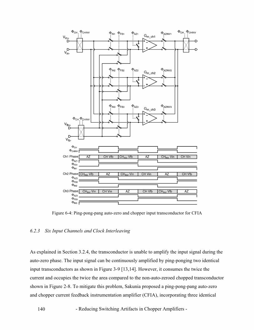
- Reducing Switching Artifacts in Chopper Amplifiers - 140
6.2.3 Six Input Channels and Clock Interleaving
As explained in Section 3.2.4, the transconductor is unable to amplify the input signal during the
auto-zero phase. The input signal can be continuously amplified by ping-ponging two identical
input transconductors as shown in Figure 3-9 [13,14]. However, it consumes the twice the
current and occupies the twice the area compared to the non-auto-zeroed chopped transconductor
shown in Figure 2-8. To mitigate this problem, Sakunia proposed a ping-pong-pang auto-zero
and chopper current feedback instrumentation amplifier (CFIA), incorporating three identical
Figure 6-4: Ping-pong-pang auto-zero and chopper input transconductor for CFIA

- Reducing Switching Artifacts in Chopper Amplifiers - 141
input transconductor channels as shown in Figure 6-4 [15]. The timing diagram shows that while
one channel is auto-zeroed, the other two work as input and feedback transconductors, one at a
time. In this case, the three transconductors together consume 1.5 times the amount of current of
a basic non-auto-zeroed CFIA with two transconductors.
Another remaining problem is that the various previous ripple reduction techniques only
reduce the up-modulated ripple without reducing the glitches caused by charge injection [13-19].
As explained in Chapters 2 and 3, while the ripple can be reduced by a factor equal to the auto-
zeroing loop gain, the glitches increase with the size of the switches and thus can result in the
higher noise PSD.
Figure 6-5 (a) presents the proposed input transconductor in its entirety, consisting of six
identical channels Ch1-6 in parallel. This transconductor reduces both the ripple and glitches, as
well as the extra current consumption for the auto-zeroing. Each channel consists of the
capacitively-coupled auto-zeroed and chopped transconductor shown in Figure 6-3, and operates
with identical and interleaved timing phases as shown in Figure 6-5 (b). Each channel goes
through the PC, AZ, CH, and CHINV phases. At any given time, one channel is in the PC phase,
while another channel is in the AZ phase, and the other four channels are in either the CH or
CHINV phases, thus amplifying the input signal in parallel. This reduces the required
transconductance of Gm1 and the width of the switches in each channel. Therefore, to achieve the
same in-band noise PSD, all six input transconductors only consume 1.5 more current than the
non-auto-zeroed chopped transconductor shown in Figure 2-8.
The current consumption can be further reduced by increasing the number of channels
operating in the CH or CHINV phases relative to the total number of channels, for instance having
a total of eight channels and assigning one channel to the PC, another channel to the AZ, and the
other six channels to the CH or CHINV phases. This, however, decreases the amount of settling
time available for the PC and AZ phases during the full operating period, and thus increases the
required bandwidth and therefore also the current consumption of CM-buf and GmAZ. Moreover,
the die size will also increase, due to the layout spacing required between each channel.
Therefore, the total channel count of six is used to optimize the overall current consumption and
the die size.

- Reducing Switching Artifacts in Chopper Amplifiers - 142
Figure 6-5: Proposed overall input transconductor consisting of six channels: (a) circuit diagram; (b) timing diagram
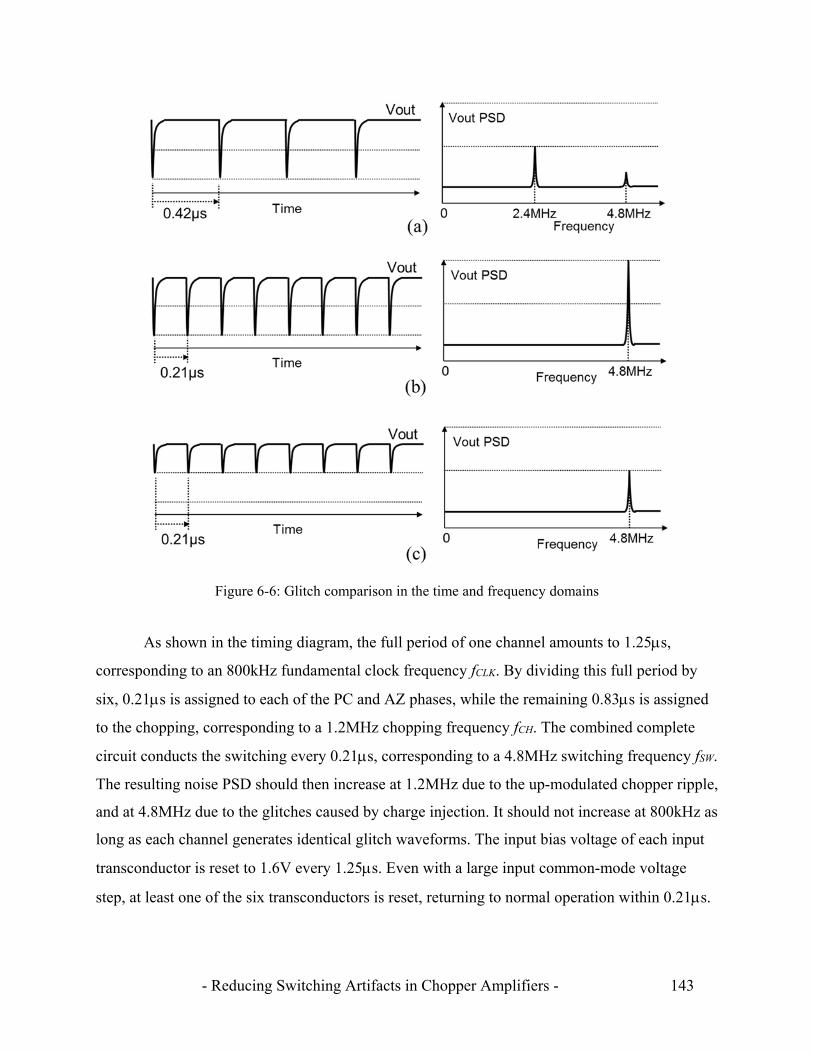
- Reducing Switching Artifacts in Chopper Amplifiers - 143
As shown in the timing diagram, the full period of one channel amounts to 1.25s,
corresponding to an 800kHz fundamental clock frequency fCLK. By dividing this full period by
six, 0.21s is assigned to each of the PC and AZ phases, while the remaining 0.83s is assigned
to the chopping, corresponding to a 1.2MHz chopping frequency fCH. The combined complete
circuit conducts the switching every 0.21s, corresponding to a 4.8MHz switching frequency fSW.
The resulting noise PSD should then increase at 1.2MHz due to the up-modulated chopper ripple,
and at 4.8MHz due to the glitches caused by charge injection. It should not increase at 800kHz as
long as each channel generates identical glitch waveforms. The input bias voltage of each input
transconductor is reset to 1.6V every 1.25s. Even with a large input common-mode voltage
step, at least one of the six transconductors is reset, returning to normal operation within 0.21s.
Figure 6-6: Glitch comparison in the time and frequency domains
- Reducing Switching Artifacts in Chopper Amplifiers - 144
The complete input transconductor proposed results in a smaller magnitude for the glitch
per individual switching, thanks to the reduced size of the switches. Figure 6-6 illustrates the
comparison of the expected output voltage waveform VOUT and noise PSD from three circuits:
the two channel circuit shown in Figure 3-9 with fCH = 1.2MHz (Figure 6-6 (a)), the same two
channel circuit but with fCH = 2.4MHz (Figure 6-6 (b)), and the six channel circuit shown in
Figure 6-5 with the interleaved fCH = 1.2MHz (Figure 6-6 (c)). For simplicity, the figure only
illustrates the glitches caused by charge injection, but not the up-modulated chopper ripple. First,
comparing Figure 6-6 (b) with Figure 6-6 (a) shows that the glitches occur more frequently and
that each one has the same magnitude. As a result, the peak PSD is pushed up to 4.8MHz, but its
magnitude increases, which will not relax the requirements of the low-pass filter. Moreover,
higher chopping frequency will increase the charge injection generated per unit of time, hence
the DC errors. Next, comparing Figure 6-6 (c) with Figure 6-6 (a) shows that the glitches occur
more frequently but that each one has a smaller magnitude, and thus the energy is spread out in
the time domain without increasing the charge injection generated per unit of time. As a result,
the peak PSD is pushed up to 4.8MHz without increasing the magnitude. This then relaxes the
requirements of the low-pass filter, and thus extends the usable signal bandwidth.
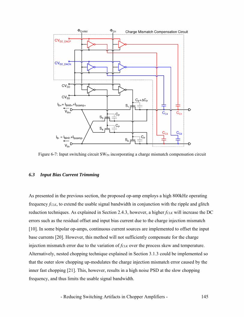
- Reducing Switching Artifacts in Chopper Amplifiers - 145
6.3 Input Bias Current Trimming
As presented in the previous section, the proposed op-amp employs a high 800kHz operating
frequency fCLK, to extend the usable signal bandwidth in conjunction with the ripple and glitch
reduction techniques. As explained in Section 2.4.3, however, a higher fCLK will increase the DC
errors such as the residual offset and input bias current due to the charge injection mismatch
[10]. In some bipolar op-amps, continuous current sources are implemented to offset the input
base currents [20]. However, this method will not sufficiently compensate for the charge
injection mismatch error due to the variation of fCLK over the process skew and temperature.
Alternatively, nested chopping technique explained in Section 3.1.3 could be implemented so
that the outer slow chopping up-modulates the charge injection mismatch error caused by the
inner fast chopping [21]. This, however, results in a high noise PSD at the slow chopping
frequency, and thus limits the usable signal bandwidth.
Figure 6-7: Input switching circuit SWIN incorporating a charge mismatch compensation circuit
- Reducing Switching Artifacts in Chopper Amplifiers - 146
6.3.1 Input Switching Circuit Employing a Charge Mismatch Compensation Circuit
Figure 6-7 presents the proposed input switching circuit SWIN, incorporating a charge mismatch
compensation circuit. The four NMOS switches S1-4 conduct the switching operation required for
the auto-zeroing and the chopping, and are driven by positive and negative clock supplies CVDD
and CVSS through inverters. Let us assume S1 is associated with a coupling capacitor CP+∆CP,
while each of the other three switches is associated with CP. As explained in Section 2.4.3, this
capacitance mismatch ∆CP causes a charge injection mismatch per clock period 1/fCLK,
generating initial input bias currents Ibinit+ and Ibinit– equal to:
)( SSDDPCLKbinitbinit CVCVCfII , (6-1)
)( SSDDPCLKbinitbinit CVCVCfII . (6-2)
To offset these error currents, the charge mismatch compensation circuit can inject charge
mismatches with opposite polarity through four metal-metal coupling capacitors CC1-4. An
adjustable positive supply CVDD_DACP drives CC1 and CC3, while another adjustable positive
supply CVDD_DACN drives CC2 and CC4. By adjusting these supply voltages, the resulting
compensation input bias currents Ibcomp+ and Ibcomp– can be controlled to allow:
)(2 __41 DACNDDDACPDDCCLKbcompbcomp CVCVCfII , (6-3)
)(2 __41 DACNDDDACPDDCCLKbcompbcomp CVCVCfII . (6-4)
CC1-4 = 2fF is only one-tenth of CP, which will not significantly increase the absolute amount of
charge injection nor, consequently, the magnitude of transient glitches. The resulting input bias
currents Ib+ and Ib– are given by:
bcompbinitb III , (6-5)
)( bcompbinitb III . (6-6)
Both Ib+ and Ib–will be pushed toward zero by adjusting Ibcomp = –Ibinit.
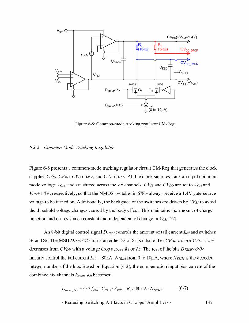
- Reducing Switching Artifacts in Chopper Amplifiers - 147
6.3.2 Common-Mode Tracking Regulator
Figure 6-8 presents a common-mode tracking regulator circuit CM-Reg that generates the clock
supplies CVSS, CVDD, CVDD_DACP, and CVDD_DACN. All the clock supplies track an input common-
mode voltage VCM, and are shared across the six channels. CVSS and CVDD are set to VCM and
VCM+1.4V, respectively, so that the NMOS switches in SWIN always receive a 1.4V gate-source
voltage to be turned on. Additionally, the backgates of the switches are driven by CVSS to avoid
the threshold voltage changes caused by the body effect. This maintains the amount of charge
injection and on-resistance constant and independent of change in VCM [22].
An 8-bit digital control signal DTRIM controls the amount of tail current Itail and switches
S5 and S6. The MSB DTRIM<7> turns on either S5 or S6, so that either CVDD_DACP or CVDD_DACN
decreases from CVDD with a voltage drop across R1 or R2. The rest of the bits DTRIM<6:0>
linearly control the tail current Itail = 80nA NTRIM from 0 to 10A, where NTRIM is the decoded
integer number of the bits. Based on Equation (6-3), the compensation input bias current of the
combined six channels Ibcomp_6ch becomes:
TRIMTRIMCCLKchbcomp NRSCfI nA 8026 2,1416_ , (6-7)
Figure 6-8: Common-mode tracking regulator CM-Reg
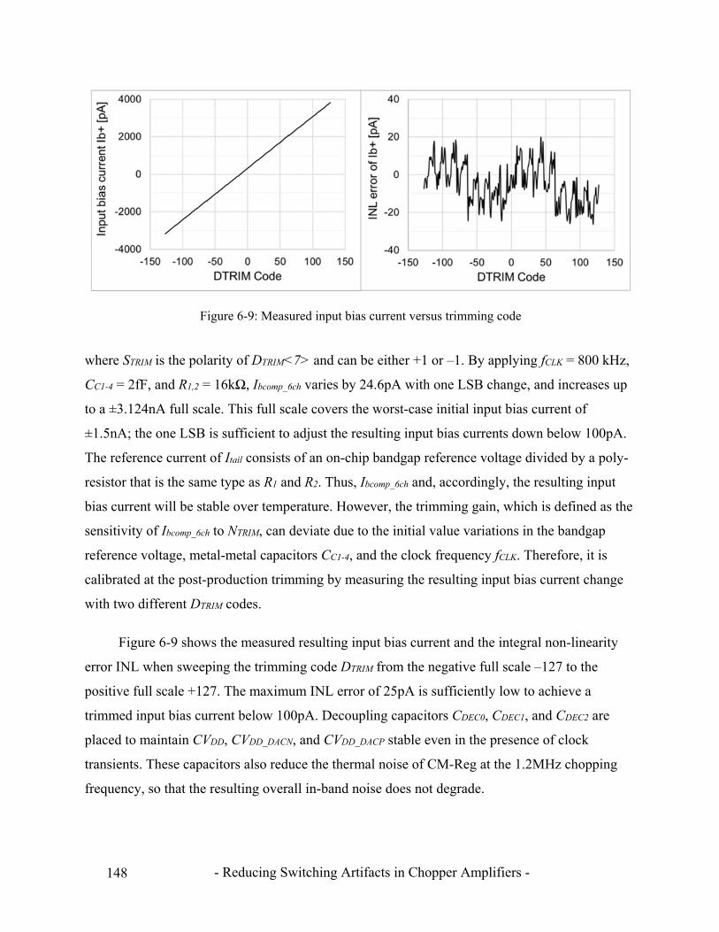
- Reducing Switching Artifacts in Chopper Amplifiers - 148
where STRIM is the polarity of DTRIM<7> and can be either +1 or –1. By applying fCLK = 800 kHz,
CC1-4 = 2fF, and R1,2 = 16kΩ, Ibcomp_6ch varies by 24.6pA with one LSB change, and increases up
to a ±3.124nA full scale. This full scale covers the worst-case initial input bias current of
±1.5nA; the one LSB is sufficient to adjust the resulting input bias currents down below 100pA.
The reference current of Itail consists of an on-chip bandgap reference voltage divided by a poly-
resistor that is the same type as R1 and R2. Thus, Ibcomp_6ch and, accordingly, the resulting input
bias current will be stable over temperature. However, the trimming gain, which is defined as the
sensitivity of Ibcomp_6ch to NTRIM, can deviate due to the initial value variations in the bandgap
reference voltage, metal-metal capacitors CC1-4, and the clock frequency fCLK. Therefore, it is
calibrated at the post-production trimming by measuring the resulting input bias current change
with two different DTRIM codes.
Figure 6-9 shows the measured resulting input bias current and the integral non-linearity
error INL when sweeping the trimming code DTRIM from the negative full scale –127 to the
positive full scale +127. The maximum INL error of 25pA is sufficiently low to achieve a
trimmed input bias current below 100pA. Decoupling capacitors CDEC0, CDEC1, and CDEC2 are
placed to maintain CVDD, CVDD_DACN, and CVDD_DACP stable even in the presence of clock
transients. These capacitors also reduce the thermal noise of CM-Reg at the 1.2MHz chopping
frequency, so that the resulting overall in-band noise does not degrade.
Figure 6-9: Measured input bias current versus trimming code
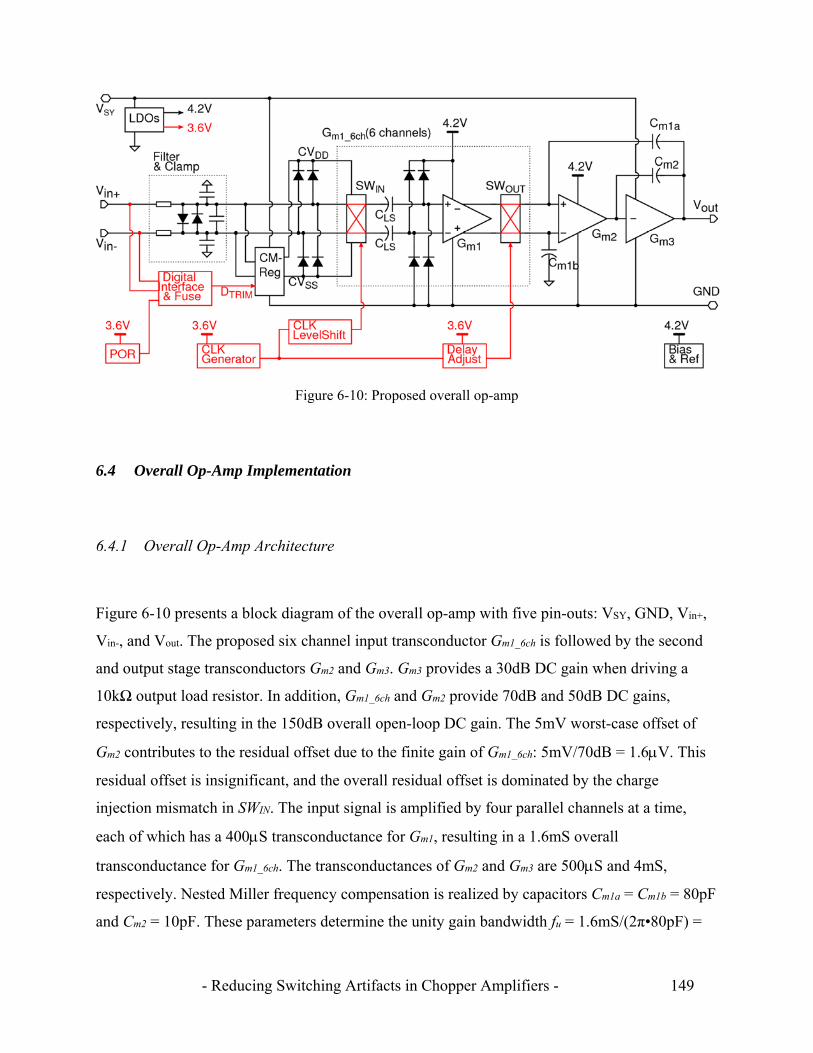
- Reducing Switching Artifacts in Chopper Amplifiers - 149
6.4 Overall Op-Amp Implementation
6.4.1 Overall Op-Amp Architecture
Figure 6-10 presents a block diagram of the overall op-amp with five pin-outs: VSY, GND, Vin+,
Vin-, and Vout. The proposed six channel input transconductor Gm1_6ch is followed by the second
and output stage transconductors Gm2 and Gm3. Gm3 provides a 30dB DC gain when driving a
10kΩ output load resistor. In addition, Gm1_6ch and Gm2 provide 70dB and 50dB DC gains,
respectively, resulting in the 150dB overall open-loop DC gain. The 5mV worst-case offset of
Gm2 contributes to the residual offset due to the finite gain of Gm1_6ch: 5mV/70dB = 1.6V. This
residual offset is insignificant, and the overall residual offset is dominated by the charge
injection mismatch in SWIN. The input signal is amplified by four parallel channels at a time,
each of which has a 400S transconductance for Gm1, resulting in a 1.6mS overall
transconductance for Gm1_6ch. The transconductances of Gm2 and Gm3 are 500S and 4mS,
respectively. Nested Miller frequency compensation is realized by capacitors Cm1a = Cm1b = 80pF
and Cm2 = 10pF. These parameters determine the unity gain bandwidth fu = 1.6mS/(2π•80pF) =
Figure 6-10: Proposed overall op-amp
- Reducing Switching Artifacts in Chopper Amplifiers - 150
3.2MHz and the second pole fp2 = 500S/(2π•10pF) = 8.0MHz. The third pole is created at the
output with an external load CL. This pole can be pushed to a higher frequency with the cascode
Miller compensation technique [19], the circuit of which will be discussed in Section 6.4.3
below.
During the production test, the initial input bias current Ibinit_6ch is measured externally,
and DTRIM code is provided through an input digital interface. The determined DTRIM code is
stored in an on-chip polyfuse memory array, which is read every power up cycle triggered by an
on-chip power-on reset circuit POR. Therefore, after the post-production trimming is complete,
the op-amp works as a stand-alone op-amp without relying on external digital resources.
The selected process is based on a 0.18m CMOS technology augmented by 5V CMOS
and 60V DMOS transistors. The 5V CMOS transistor can handle gate-source and drain-source
voltages up to 6V, and can be formed in an isolated backgate with a more than 60V breakdown
voltage to the substrate. The 60V DMOS transistor can handle gate-source voltages up to 6V and
drain-source voltages up to 60V, although it occupies a larger area and generates higher offset
and noise than the 5V CMOS transistor. Therefore, the key blocks in the signal chain, including
SWIN, Gm1, SWOUT, and Gm2, consist of the 5V CMOS transistors, while the 60V DMOS
transistors are used to isolate these blocks from high supply and input voltages. A CM-Reg
circuit maintains the supply voltage difference CVDD – CVSS to 1.4V to protect SWIN. Since CLS
level-shifts the input signals down to 1.6V, Gm1, SWOUT, and Gm2 are all supplied by a 4.2V
regulated voltage. Additionally, an input RC filter and clamping diodes are implemented to
protect SWIN and Gm1 from high voltage transient inputs.
Metal-metal fringing capacitors with a more than 60 V breakdown are used for the input
RC filter, CLS, Cm1a, Cm1b, and Cm2. The clocks are generated with a 3.6 V regulated supply, and a
clock level shifter is used before SWIN. A delay circuit is added before SWOUT, to align the clock
phases at SWIN and SWOUT. The overall op-amp consumes an 840A supply current: 320A for
Gm1_6ch, 180A for Gm2, 180A for Gm3, 50A for CM-Reg, 50A for the clock generator and
level shifter, and 60A for the rest including the POR, LDOs, and bias circuits.
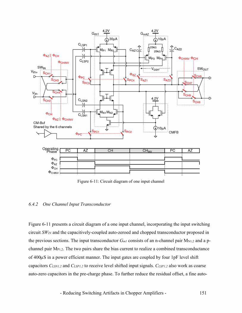
- Reducing Switching Artifacts in Chopper Amplifiers - 151
6.4.2 One Channel Input Transconductor
Figure 6-11 presents a circuit diagram of a one input channel, incorporating the input switching
circuit SWIN and the capacitively-coupled auto-zeroed and chopped transconductor proposed in
the previous sections. The input transconductor Gm1 consists of an n-channel pair MN1,2 and a p-
channel pair MP1,2. The two pairs share the bias current to realize a combined transconductance
of 400S in a power efficient manner. The input gates are coupled by four 1pF level shift
capacitors CLSN1,2 and CLSP1,2 to receive level shifted input signals. CLSP1,2 also work as coarse
auto-zero capacitors in the pre-charge phase. To further reduce the residual offset, a fine auto-
Figure 6-11: Circuit diagram of one input channel
- Reducing Switching Artifacts in Chopper Amplifiers - 152
zero is conducted by an auto-zeroed transconductor GmAZ with another p-channel pair MP3,4 and
two 1pF auto-zero capacitors CAZ1,2. A common-mode feedback circuit CMFB controls an
NMOS tail current source, to keep the output common-mode voltage at 1.8V in all operating
phases.
As discussed in Section 6.2.3, one channel goes through the pre-charge PC, the auto-zero
AZ, the chopping CH, and the inverting-chop CHINV phases. During the PC phase, a non-
inverting input voltage Vin+ charges the bottom plates of CLSN1,2 and CLSP1,2 through switches
SCH1 and SCH4. Meanwhile, the common-mode buffer CM-Buf charges the top plates of CLSN1,2
through switches SPC1,2. Additionally, switches SPC3,4 form feedback around Gm1 to charge the
top plates of CLSP1,2. At the end-of this phase, SPC1-4 turn off, and CLSN1,2 and CLSP1,2 become
floating voltage sources. At the same time, a 3mV maximum initial offset for Gm1 is sampled by
CLSP1,2, and thus auto-zeroed. Instead, a maximum charge injection mismatch ΔqPC1-4 = 0.1fC
flows into CLSN1,2 and CLSP1,2 and dominates the residual offset in this phase Vos,resPC = 0.1fC/1pF
= 100V. In the next AZ phase, GmAZ forms a fine auto-zero feedback through switches SAZ1,2 to
cancel Vos,resPC. It is degenerated with two 25kΩ resistors, so that the transconductance is only
25S, i.e. 16 times lower than that of Gm1. The resulting correction voltage Vcorr =
(Gm1/GmAZ)•Vos,resPC is sampled by CAZ1,2 along with the final residual error Vcorrerr. When the CH
phase starts, the differential inputs and outputs of Gm1 become connected to the signal path
through the input and output switches SCH1,2 and SCH5,6. Moving to the CHINV phase, SWIN and
SWOUT invert the polarity by closing SCH3,4 and SCH7,8, to up-modulate the final residual error
Vcorrerr to the 1.2MHz chopping frequency fCH.
Based on Equations (2-6) and (2-7), the magnitude of the up-modulated input error
voltage VGm1err is given by:
AZ
AZ
m
mAZresPCos
vAZcorrerr
m
mAZerrGm C
q
G
GV
AV
G
GV
1,
11
1, (6-8)
where AvAZ = 50dB is the loop gain of the fine auto-zero feedback, and ΔqAZ1,2= 0.05fC is the
maximum charge injection mismatch of SAZ1,2. Additionally, the sampled noise charge is added
along with ΔqAZ1,2. First, Vos,resPC = 100V is suppressed by AvAZ, only resulting in a 0.3µV error.
Second, ΔqAZ1,2 is attenuated by GmAZ/Gm1 = 1/16, resulting in a 3.1µV error. The combined
- Reducing Switching Artifacts in Chopper Amplifiers - 153
3.4µV error per channel is averaged out with the other three channels operating in parallel, and
thus further reduced to 1.7µV. It is insignificant, and thus is hidden by the 12.5nV/√Hz up-
modulated sampled noise PSD at fCH, as will be shown in the measurement result.
Thanks to the proposed dual coarse-fine auto-zero technique, GmAZ only has to correct the
100V maximum residual offset rather than the 3mV initial offset, resulting in two benefits.
First, the maximum correction voltage Vcorr is only 1.6mV, and thus does not cause a significant
glitch when switching the six channels as explained in Section 3.2.4. Second, the fine auto-zero
loop has the relaxed gain requirement, and thus can consist of a single transconductor stage
without requiring the active integrator used in [14].
A high DC CMRR should be expected since CLSN1,2 and CLSP1,2 block the DC common-
mode voltage. On the other hand, AC common-mode noise will be coupled to Gm1, and then
rejected by the CMFB with a 4MHz loop bandwidth.
6.4.3 Second and Output Transconductors
Figure 6-12 presents the second and output stage transconductors Gm2 and Gm3 together. Gm2
consists of a p-channel differential pair MP21,22 followed by a folded cascode stage. The p-
channel differential pair is supplied by the regulated 4.2V supply voltage, while the output
common-mode voltage of Gm1 is maintained at 1.8V. In the folded cascode stage, 60V NDMOS
transistors MN25,26 keep the potentials of four low side 5V NMOS transistors MN21-24 below 4V.
Similarly, a 60V PDMOS transistor MP27 keeps the potentials of four high side 5V PMOS
transistors MP23-26 within 4V of VSY.

- Reducing Switching Artifacts in Chopper Amplifiers - 154
The folded cascode stage drives the gates of low and high side transistors MN31 and MP31 to form
a class-AB output transconductor Gm3. Each of these gate voltages VGm3N and VGm3P is clamped
with three series diodes, and thus is kept within 4V of each supply rail even in the presence of
output transient or overcurrent events. Additionally, cascode DMOS transistors MN32 and MP32
keep the drain potentials of MN31 and MP31 within 3V of each supply rail. Two 5pF frequency
compensation capacitors Cm2N and Cm2P together represent Cm2 in Figure 6-10, and they are fed
back to the sources of MN23 and MP25, respectively. This cascode Miller frequency compensation,
as presented in [19], pushes the third pole, occurring at the output of Gm3, to a higher frequency,
and thus reduces the current consumption of Gm3 required to make the op-amp stable.
Figure 6-12: The second and output stage transconductors Gm2 and Gm3

- Reducing Switching Artifacts in Chopper Amplifiers - 155
6.4.4 Clock Generator and Level Shifter
Figure 6-13 presents the clock generator and level shifter, which provide the timing clocks to
SWIN, SWOUT, SPC1-4, and SAZ1,2 in Gm1_6chs. The clock generator consists of a 4.8MHz oscillator
and a clock divider to generate six interleaved 800kHz clocks ΦCLK1-6. As shown in the figure,
the clock generator is supplied by internally regulated 3.6V. The resulting 3.6V output clock
level is sufficiently high to turn on the NMOS switches in SWOUT, SPC1-4, and SAZ1,2, the source
potentials of which are maintained at either 1.6V or 1.8V. On the other hand, as shown in Figure
6-7, the clocks need to be level-shifted to CVDD and CVSS in order to turn the NMOS switches in
SWIN on and off, respectively. The clock level shifter consists of a 20µA tail current source, six
source-coupled input NMOS switches MN1-6, six NDMOS cascode transistors, and six 80kΩ load
resistors RL1-6 supplied by CVDD. Based on ΦCLK1-6, the 20µA current flows into either one of the
Figure 6-13: The clock generator and level shifter
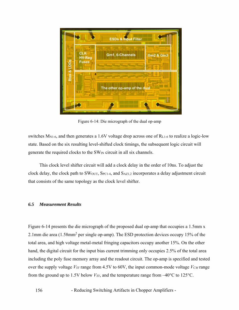
- Reducing Switching Artifacts in Chopper Amplifiers - 156
switches MN1-6, and then generates a 1.6V voltage drop across one of RL1-6 to realize a logic-low
state. Based on the six resulting level-shifted clock timings, the subsequent logic circuit will
generate the required clocks to the SWIN circuit in all six channels.
This clock level shifter circuit will add a clock delay in the order of 10ns. To adjust the
clock delay, the clock path to SWOUT, SPC1-4, and SAZ1,2 incorporates a delay adjustment circuit
that consists of the same topology as the clock level shifter.
6.5 Measurement Results
Figure 6-14 presents the die micrograph of the proposed dual op-amp that occupies a 1.5mm x
2.1mm die area (1.58mm2 per single op-amp). The ESD protection devices occupy 15% of the
total area, and high voltage metal-metal fringing capacitors occupy another 15%. On the other
hand, the digital circuit for the input bias current trimming only occupies 2.5% of the total area
including the poly fuse memory array and the readout circuit. The op-amp is specified and tested
over the supply voltage VSY range from 4.5V to 60V, the input common-mode voltage VCM range
from the ground up to 1.5V below VSY, and the temperature range from –40°C to 125°C.
Figure 6-14: Die micrograph of the dual op-amp
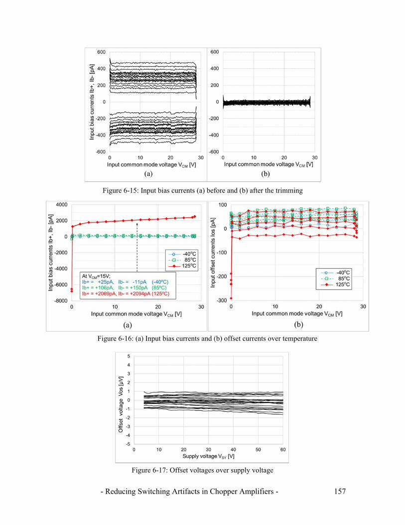
- Reducing Switching Artifacts in Chopper Amplifiers - 157
Figure 6-15: Input bias currents (a) before and (b) after the trimming
Figure 6-16: (a) Input bias currents and (b) offset currents over temperature
Figure 6-17: Offset voltages over supply voltage

- Reducing Switching Artifacts in Chopper Amplifiers - 158
Figure 6-15 (a) and (b) shows the input bias currents before and after the trimming,
respectively. The same 20 op-amp units are tested with a VSY of 30V and VCM range of 0V to
28.5V. Before the trimming, the input bias currents are distributed up to ±500pA, all of which
are almost constant thanks to the common-mode tracking regulator CM-Reg. These constant
input bias currents can be corrected with a single bias point trimming with VSY = 5.5V, VCM =
2.75V, and ambient temperature. After the trimming, the worst-case input bias current is reduced
to ±40pA in the middle of VCM. This increases up to ±90pA near the upper and lower limits of
the VCM range, because one of the clock supply voltages CVSS or CVDD saturates near the ground
or VSY. After adding the error band due to the part-part distribution and the test inaccuracy, the
maximum input bias current is specified at ±150pA which would be ±1.5nA without trimming.
Figure 6-16 (a) shows the input bias currents of one op-amp unit at three different temperatures:
–40°C, 85°C, and 125°C. At 125°C, the currents increase above +2nA due to the increased ESD
diode leakage. Note that each input pin is clamped against VSY and GND pins through two
diodes, and that the diode connected between input and GND generates more reverse leakage
current due to its structure. Moreover, the currents at 125°C quickly drops below –6nA near VCM
= 0V, because the common-mode tracking regulator CM-Reg saturates, which drives the source-
backgate diodes of the input chopper switches slightly into forward-bias condition. Figure 6-16
(b) shows the input offset currents of five op-amp units to evaluate residual charge injection
mismatch over temperature. At 125°C, the offset currents drop to –300pA near VCM = 0V due to
the increased ESD diode leakage current mismatches. The input offset currents are less than
±100pA in any other conditions, demonstrating the temperature stability of the proposed charge
mismatch compensation circuit. Figure 6-17 shows the offset voltages of the 20 op-amp units
over a VSY from 4.5V to 60V. Additionally, Figure 6-18 shows the offset voltages over a VCM
from 0V to 28.5V with VSY = 30V. Similar to the input bias currents, any given unit exhibits
relatively constant offset with the changes in VSY and VCM. As a result, the minimum DC CMRR
and PSRR are 145dB and 150dB, respectively. Figure 6-19 (a) and (b) shows the histograms of
the offset voltage and the temperature drift, the maximum values of which are well below ±5V
and 20nV/°C, respectively. Figure 6-20 shows the AC CMRR and PSRR versus the frequencies.
More rejection is obtained when stimulating the VSY pin (PSRR+), rather than the GND pin
(PSRR–), because of the use of on-chip LDOs.

- Reducing Switching Artifacts in Chopper Amplifiers - 159
Figure 6-18: Offset voltages over specified VCM
Figure 6-19: Histograms of (a) the offset voltage and (b) the temperature drift
Figure 6-20: CMRR and PSRR over the frequency
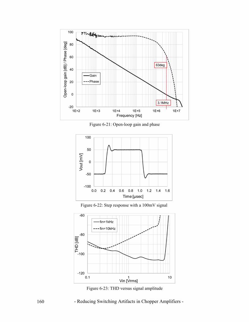
- Reducing Switching Artifacts in Chopper Amplifiers - 160
Figure 6-21: Open-loop gain and phase
Figure 6-22: Step response with a 100mV signal
Figure 6-23: THD versus signal amplitude
- Reducing Switching Artifacts in Chopper Amplifiers - 161
Next, the measured AC performance is shown, while the op-amp is configured for unity
gain with VSY = 30V and is driving 100pF unless otherwise stated. Figure 6-21 shows the open-
loop gain and phase. It can be seen that the op-amp achieves a 3.1MHz unity gain bandwidth fu
and a 63-degree phase margin PM. Testing twelve units with the three different VSY at 5V, 30V,
and 60V, the maximum variations in fu and PM are ±0.24MHz and ±1.0 degree, respectively. No
pole-zero doublet is observed below fu, since the op-amp consists of a single gain path. Figure 6-
22 shows the 100mV step response, where the output settles to a 0.1% error band with less than
0.4s. Figure 6-23 shows the THD versus signal amplitude Vin. With the signal frequency fin =
1kHz, it achieves a –106dB peak performance, and rises above –40dB when Vin increases beyond
10Vrms and approaches the supply rails. With fin = 10kHz, it achieves a –95dB peak, and rises
above –40 dB, when Vin increases beyond 7.5Vrms and reaches the slew rate limit.
Figure 6-24 shows the measured voltage noise PSD, along with the one simulated by the
SpectreRF periodic noise analysis [23]. The measurement indicates a 5.8nV/√Hz in-band noise
PSD and a 0.15Hz 1/f noise corner frequency. At higher frequencies, it has two humps at
1.2MHz and 6MHz, as well as two peak PSDs at 800kHz and 4.8MHz. The first PSD hump of
12.4nV/√Hz is the up-modulated sampled noise as explained in Section 6.4.2. The second PSD
hump of 23.0nV/√Hz is dominated by the thermal noise of Gm2 and Gm3, due to the gain
reduction of Gm1 at a higher frequency. These measured humps and the in-band noise PSD are
reasonably correlated with the simulation. On the other hand, the two peak PSDs are due to
glitches caused by the charge injection, and thus are not included in the simulation. The
magnitudes differ for each op-amp unit as shown in the histogram in Figure 6-25. Thanks to the
proposed interleaving technique, the majority of the glitch energy is located at 4.8MHz.
Consequently, 80% of the units have sufficiently low peak PSDs at 800kHz, which are hidden by
the noise floor. The remaining 20% of the units show that the peak PSDs are higher than the
noise floor, because of the mismatched glitch waveform among the six channels. With any
degree of mismatch, the glitch energy at 800kHz is only a fraction of that at 4.8MHz, so that its
maximum value is still 27.5 nV/√Hz among the 20 op-amp units.
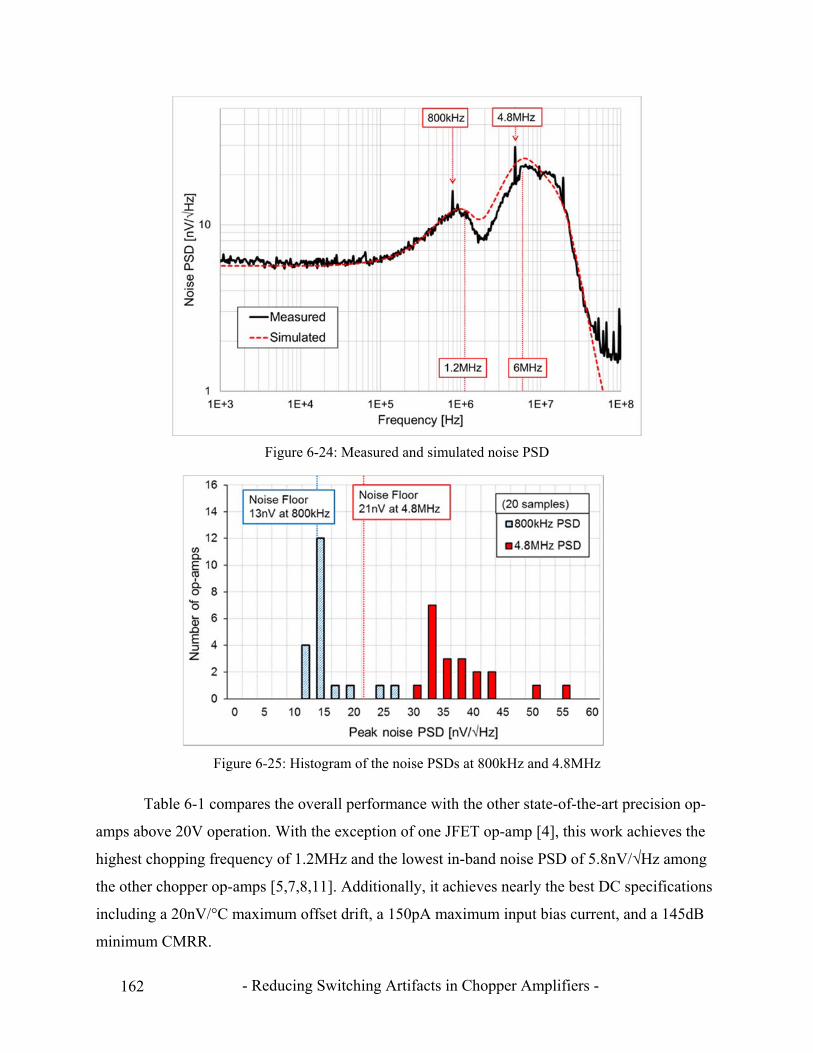
- Reducing Switching Artifacts in Chopper Amplifiers - 162
Table 6-1 compares the overall performance with the other state-of-the-art precision op-
amps above 20V operation. With the exception of one JFET op-amp [4], this work achieves the
highest chopping frequency of 1.2MHz and the lowest in-band noise PSD of 5.8nV/√Hz among
the other chopper op-amps [5,7,8,11]. Additionally, it achieves nearly the best DC specifications
including a 20nV/°C maximum offset drift, a 150pA maximum input bias current, and a 145dB
minimum CMRR.
Figure 6-24: Measured and simulated noise PSD
Figure 6-25: Histogram of the noise PSDs at 800kHz and 4.8MHz

- Reducing Switching Artifacts in Chopper Amplifiers - 163
6.6 Conclusion
An auto-zero and chopper op-amp operating in the 4.5V to 60V supply range has been realized
in the 0.18m CMOS process augmented by 5V CMOS and 60V DMOS transistors. The input
transconductor is capacitively-coupled and utilizes auto-zero and chopping techniques to achieve
low offset, low ripple, and a wide input common-mode voltage range. The auto-zeroing consists
of coarse and fine auto-zero phases to sufficiently reduce the residual ripple without requiring an
active integrator stage. Moreover, it employs six parallel input channels with 800kHz interleaved
clocks to mitigate the glitches caused by charge injection. This pushes the majority of the glitch
energy up to 4.8MHz, while leaving the residual energy at 800kHz due to channel-channel
mismatches. It relaxes requirements of the low-pass filter, and thus achieves a wider usable
signal bandwidth. Furthermore, the trade-off between the chopping frequency and the DC
performance is overcome by the post-production trimming with the on-chip charge mismatch
compensation circuit, reducing the maximum input bias current from 1.5nA to 150pA.
Table 6-1: Comparison with other state-of-the-art
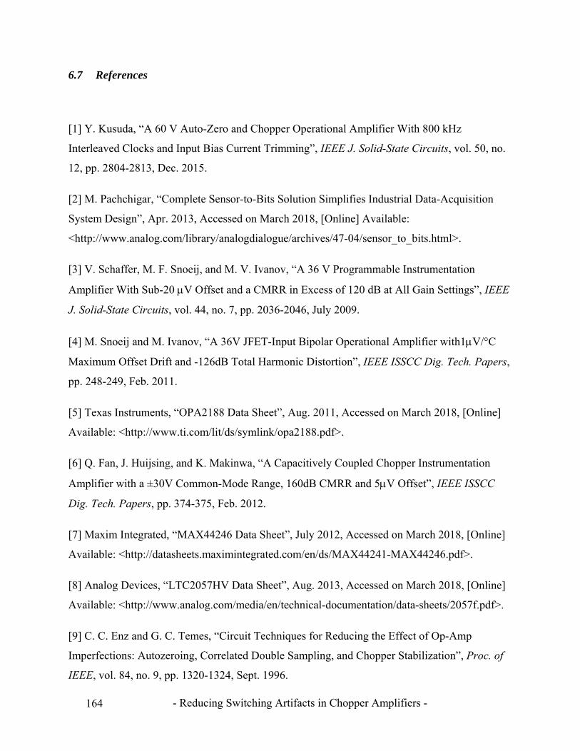
- Reducing Switching Artifacts in Chopper Amplifiers - 164
6.7 References
[1] Y. Kusuda, “A 60 V Auto-Zero and Chopper Operational Amplifier With 800 kHz
Interleaved Clocks and Input Bias Current Trimming”, IEEE J. Solid-State Circuits, vol. 50, no.
12, pp. 2804-2813, Dec. 2015.
[2] M. Pachchigar, “Complete Sensor-to-Bits Solution Simplifies Industrial Data-Acquisition
System Design”, Apr. 2013, Accessed on March 2018, [Online] Available:
<http://www.analog.com/library/analogdialogue/archives/47-04/sensor_to_bits.html>.
[3] V. Schaffer, M. F. Snoeij, and M. V. Ivanov, “A 36 V Programmable Instrumentation
Amplifier With Sub-20 V Offset and a CMRR in Excess of 120 dB at All Gain Settings”, IEEE
J. Solid-State Circuits, vol. 44, no. 7, pp. 2036-2046, July 2009.
[4] M. Snoeij and M. Ivanov, “A 36V JFET-Input Bipolar Operational Amplifier with1V/°C
Maximum Offset Drift and -126dB Total Harmonic Distortion”, IEEE ISSCC Dig. Tech. Papers,
pp. 248-249, Feb. 2011.
[5] Texas Instruments, “OPA2188 Data Sheet”, Aug. 2011, Accessed on March 2018, [Online]
Available: <http://www.ti.com/lit/ds/symlink/opa2188.pdf>.
[6] Q. Fan, J. Huijsing, and K. Makinwa, “A Capacitively Coupled Chopper Instrumentation
Amplifier with a ±30V Common-Mode Range, 160dB CMRR and 5V Offset”, IEEE ISSCC
Dig. Tech. Papers, pp. 374-375, Feb. 2012.
[7] Maxim Integrated, “MAX44246 Data Sheet”, July 2012, Accessed on March 2018, [Online]
Available: <http://datasheets.maximintegrated.com/en/ds/MAX44241-MAX44246.pdf>.
[8] Analog Devices, “LTC2057HV Data Sheet”, Aug. 2013, Accessed on March 2018, [Online]
Available: <http://www.analog.com/media/en/technical-documentation/data-sheets/2057f.pdf>.
[9] C. C. Enz and G. C. Temes, “Circuit Techniques for Reducing the Effect of Op-Amp
Imperfections: Autozeroing, Correlated Double Sampling, and Chopper Stabilization”, Proc. of
IEEE, vol. 84, no. 9, pp. 1320-1324, Sept. 1996.
- Reducing Switching Artifacts in Chopper Amplifiers - 165
[10] Q. Fan, J. Huijsing, and K. Makinwa, “Input Characteristics of a Chopped Multi-Path
Current Feedback Instrumentation Amplifier”, in Proc., 4th Int. Workshop on Advances in
Sensors and Interfaces, IWASI, pp. 61-66, June 2011.
[11] Q. Fan, J. Huijsing, and K. A. A. Makinwa, “A Multi-Path Chopper-Stabilized Capacitively
Coupled Operational Amplifier with 20V-Input-Common-Mode Range and 3V Offset”, IEEE
ISSCC Dig. Tech. Papers, pp. 176-177, Feb. 2013.
[12] Q. Fan, “Capacitively-Coupled Chopper Amplifiers”, Ph.D. Thesis, Delft University of
Technology, the Netherlands, 2013.
[13] A. T. K. Tang, “A 3V-Offset Operational Amplifier with 20nV/√Hz Input Noise PSD at
DC Employing both Chopping and Autozeroing”, IEEE ISSCC Dig. Tech. Papers, pp. 362-387,
Feb. 2002.
[14] M. Pertijs and W. J. Kindt, “A 140 dB-CMRR current-feedback instrumentation amplifier
employing ping-pong auto-zeroing and chopping”, IEEE J. Solid-State Circuits, vol. 45, no. 10,
pp.2044-2056, Oct. 2010.
[15] S. Sakunia, F. Witte, M. Pertijs, and K. A. A. Makinwa, “A Ping-Pong-Pang Current-
Feedback Instrumentation Amplifier with 0.04% Gain Error”, IEEE Symposium on VLSI
Circuits, pp. 60-61, June 2011.
[16] R. Burt and J. Zhang, “A Micropower Chopper-Stabilized Operational Amplifier using a SC
Notch Filter with Synchronous Integration inside the Continuous-Time Signal Path”, IEEE J.
Solid-State Circuits, vol. 41, no. 12, pp. 2729-2736, Dec. 2006.
[17] Y. Kusuda, “Auto Correction Feedback for Ripple Suppression in a Chopper Amplifier”,
IEEE J. Solid-State Circuits, vol. 45, no. 8, pp.1436-1445, Aug. 2010.
[18] M. Belloni, E. Bonizzoni, A. Fornasari, and F. Maloberti, “A Micropower Chopper-CDS
Operational Amplifier”, IEEE J. Solid-State Circuits, vol. 45, no. 12, pp. 2521-2529, Dec. 2010.

- Reducing Switching Artifacts in Chopper Amplifiers - 166
[19] Q. Fan, J. H. Huijsing, and K. A. A. Makinwa, “A 21 nV/√Hz Chopper-Stabilized Multi-
Path Current-Feedback Instrumentation Amplifier With 2 V Offset”, IEEE J. Solid-State
Circuits, vol. 47, no. 2, pp. 464-475, Feb. 2012.
[20] Analog Devices, “MT-038 Tutorial Op Amp Input Bias Current”, Accessed on March 2018,
[Online] Available: <http://www.analog.com/media/en/training-seminars/tutorials/MT-038.pdf>.
[21] A. Bakker, K. Thiele, and J. H. Huijsing, “A CMOS Nested-Chopper Instrumentation
Amplifier with 100-nV Offset”, IEEE J. Solid-State Circuits, vol. 35, no. 12, pp. 1877-1883,
Dec. 2000.
[22] Y. Kusuda, “A 5.6 nV/√Hz Chopper Operational Amplifier Achieving a 0.5 V Maximum
Offset Over Rail-to-Rail Input Range with Adaptive Clock Boosting Technique”, IEEE J. Solid-
State Circuits, vol. 51, no. 9, pp. 2119-2128, Sept. 2016.
[23] K. Kundert, “Simulating Switched-Capacitor Filters with SpectreRF”, July 2006, Accessed
on March 2018, [Online] Available: <http://www.designers-guide.org/Analysis/sc-filters.pdf>.
- Reducing Switching Artifacts in Chopper Amplifiers - 167
Chapter 7
Conclusion
This chapter summarizes the work accomplished in this thesis and draws some conclusions.
First, Section 7.1 compares the performances among the three proposed chopper op-amps, and
reviews their evolution. In particular, a comparison is presented of the DC errors and the noise
PSD peaks due to switching artifacts, so that the proposed switching artifact reduction techniques
can be evaluated. Next, Section 7.2 compares the achieved performances with the other state-of-
the-art designs. In Section 7.3, some suggestions for future work are presented. Lastly, Section
7.4 lists the original contributions of this work.
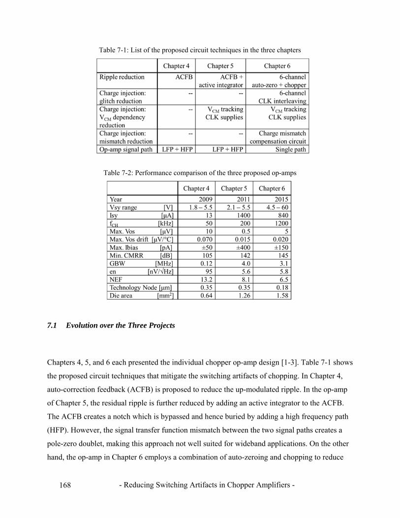
- Reducing Switching Artifacts in Chopper Amplifiers - 168
7.1 Evolution over the Three Projects
Chapters 4, 5, and 6 each presented the individual chopper op-amp design [1-3]. Table 7-1 shows
the proposed circuit techniques that mitigate the switching artifacts of chopping. In Chapter 4,
auto-correction feedback (ACFB) is proposed to reduce the up-modulated ripple. In the op-amp
of Chapter 5, the residual ripple is further reduced by adding an active integrator to the ACFB.
The ACFB creates a notch which is bypassed and hence buried by adding a high frequency path
(HFP). However, the signal transfer function mismatch between the two signal paths creates a
pole-zero doublet, making this approach not well suited for wideband applications. On the other
hand, the op-amp in Chapter 6 employs a combination of auto-zeroing and chopping to reduce
Table 7-1: List of the proposed circuit techniques in the three chapters
Table 7-2: Performance comparison of the three proposed op-amps
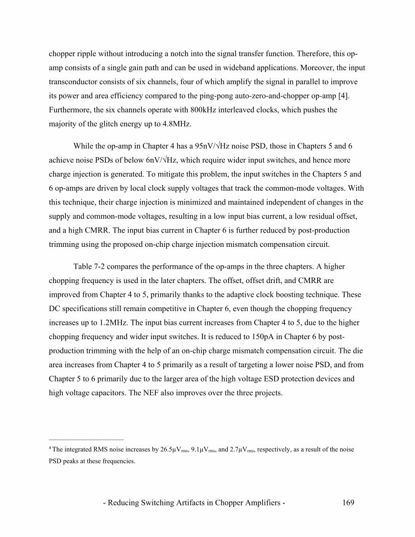
- Reducing Switching Artifacts in Chopper Amplifiers - 169
chopper ripple without introducing a notch into the signal transfer function. Therefore, this op-
amp consists of a single gain path and can be used in wideband applications. Moreover, the input
transconductor consists of six channels, four of which amplify the signal in parallel to improve
its power and area efficiency compared to the ping-pong auto-zero-and-chopper op-amp [4].
Furthermore, the six channels operate with 800kHz interleaved clocks, which pushes the
majority of the glitch energy up to 4.8MHz.
While the op-amp in Chapter 4 has a 95nV/√Hz noise PSD, those in Chapters 5 and 6
achieve noise PSDs of below 6nV/√Hz, which require wider input switches, and hence more
charge injection is generated. To mitigate this problem, the input switches in the Chapters 5 and
6 op-amps are driven by local clock supply voltages that track the common-mode voltages. With
this technique, their charge injection is minimized and maintained independent of changes in the
supply and common-mode voltages, resulting in a low input bias current, a low residual offset,
and a high CMRR. The input bias current in Chapter 6 is further reduced by post-production
trimming using the proposed on-chip charge injection mismatch compensation circuit.
Table 7-2 compares the performance of the op-amps in the three chapters. A higher
chopping frequency is used in the later chapters. The offset, offset drift, and CMRR are
improved from Chapter 4 to 5, primarily thanks to the adaptive clock boosting technique. These
DC specifications still remain competitive in Chapter 6, even though the chopping frequency
increases up to 1.2MHz. The input bias current increases from Chapter 4 to 5, due to the higher
chopping frequency and wider input switches. It is reduced to 150pA in Chapter 6 by post-
production trimming with the help of an on-chip charge mismatch compensation circuit. The die
area increases from Chapter 4 to 5 primarily as a result of targeting a lower noise PSD, and from
Chapter 5 to 6 primarily due to the larger area of the high voltage ESD protection devices and
high voltage capacitors. The NEF also improves over the three projects.
______________________ 4 The integrated RMS noise increases by 26.5µVrms, 9.1µVrms, and 2.7µVrms, respectively, as a result of the noise
PSD peaks at these frequencies.
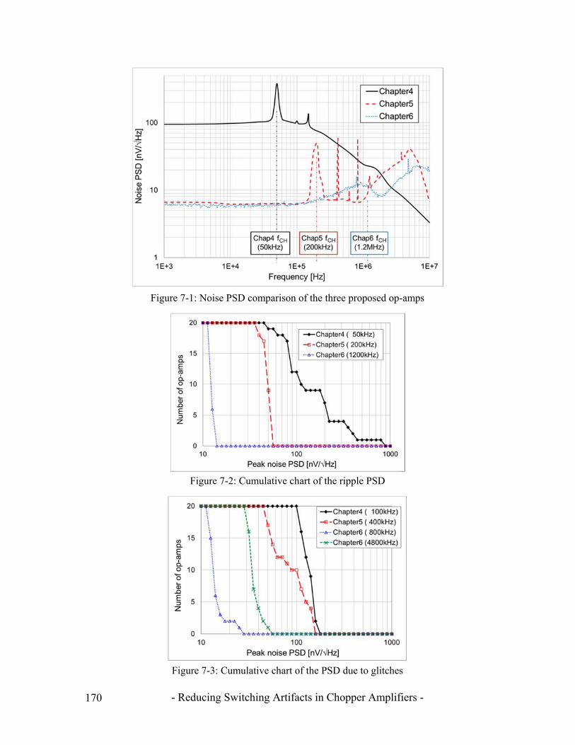
- Reducing Switching Artifacts in Chopper Amplifiers - 170
Figure 7-1: Noise PSD comparison of the three proposed op-amps
Figure 7-2: Cumulative chart of the ripple PSD
Figure 7-3: Cumulative chart of the PSD due to glitches
- Reducing Switching Artifacts in Chopper Amplifiers - 171
Figure 7-1 compares the noise PSDs of the three op-amps. All of them increase at the
chopping frequencies fCH = 50kHz, 200kHz, and 1.2MHz4 due to the up-modulated ripple.
Additionally, in Chapters 4 and 5, glitches due to charge injection cause noise PSD peaks at
2•fCH. On the other hand, in Chapter 6, the clock interleaving technique pushes the noise PSD
peak up to 4.8MHz, while leaving a residual peak PSD at 800kHz.
Figure 7-2 shows the cumulative chart of the ripple PSD magnitude at fCH by testing 20
op-amp units from each chapter. In Chapter 4, the PSD is widely distributed from 45nV/√Hz to
800nV/√Hz, since it is dominated by the initial offset in conjunction with the finite loop gain of
the ACFB. In Chapter 5, the loop gain of the ACFB is increased by the added active integrator,
which sufficiently reduces the initial offset. However, the thermal noise of the active integrator is
sampled in the SC-NF without being effectively band-limited, and is then up-modulated to
dominate the 50nV/√Hz noise PSD peak. In Chapter 6, the initial offset is sufficiently reduced by
the dual coarse-fine auto-zero technique with the single auto-zeroing transconductor stage,
resulting in a relatively low noise PSD peak in the range of 12nV/√Hz to 13nV/√Hz.
Similarly, Figure 7-3 shows the cumulative chart of the peak PSD magnitude due to
glitches. In Chapter 4, the PSD is contributed both by the thermal noise floor and the glitches,
and thus remains relatively constant in the range of 100nV/√Hz to 150nV/√Hz. In Chapter 5, on
the other hand, it has a lower thermal noise floor but higher glitch energy due to wider input
switches. Consequently, the peak PSD is widely distributed from 46nV/√Hz to 158nV/√Hz due
to various random glitch factors. In Chapter 6, the majority of the glitch energy is located at
4.8MHz, the magnitude of which is distributed from 29nV/√Hz to 54nV/√Hz. At 800kHz, 16
units out of 20 show a noise PSD below 13nV/√Hz without a peak, while the remaining 4 units
show the peak PSDs distributed up to 26nV/√Hz due to the mismatch of the glitches among the
six channels.
Based on the noise PSD in Figure 7-1, Figure 7-4 shows the integrated RMS noise over
frequency. Below fCH, the integrated noise increases linearly over frequency due to the constant
in-band noise floor. The integrated noise of the designs in Chapter 4 and 5 quickly increase
above fCH = 50kHz and 200kHz, respectively, due to relatively high peak PSDs. On the other
hand, the integrated noise of the design in Chapter 6 only increases slightly above fCH = 1.2MHz,
thanks to the proposed switching artifact reduction techniques. This provides significant

- Reducing Switching Artifacts in Chopper Amplifiers - 172
advantages, for instance reducing the integrated noise within a given signal bandwidth and/or
extending usable signal bandwidth with a given integrated noise target. For instance, for a
500kHz bandwidth, the integrated noise of the designs in Chapter 5 and 6 are 11.6μVrms and
5.4μVrms, respectively. From another perspective, to target 10μVrms input-referred noise, the
usable signal bandwidths of the designs in Chapter 5 and 6 are 400kHz and 1MHz, respectively.
Figure 7-5 shows the measured transient output waveforms of the op-amps configured for unity
gain. The design in Chapter 5 clearly shows 1.5mV peak glitches that can cause errors in
subsequent stages if not filtered. On the other hand, the glitches are invisible in the design in
Chapter 6.
Figure 7-4: Integrated RMS noise over the frequency
Figure 7-5: Transient output waveforms
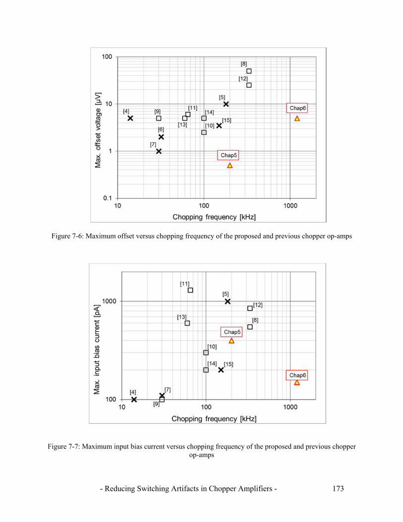
- Reducing Switching Artifacts in Chopper Amplifiers - 173
Figure 7-6: Maximum offset versus chopping frequency of the proposed and previous chopper op-amps
Figure 7-7: Maximum input bias current versus chopping frequency of the proposed and previous chopper op-amps

- Reducing Switching Artifacts in Chopper Amplifiers - 174
7.2 Benchmark
As explained in Section 2.4, chopper op-amp design involves trade-offs between the DC errors,
the chopping frequency, and the noise PSD. To compare these specifications among different
designs, Figure 7-6 plots the chopping frequency versus the maximum offsets, and Figure 7-7
plots the chopping frequency versus the maximum input bias currents. The plots [4-14] are the
specifications of previous state-of-the-art chopper op-amps that were reported before 2013, and
have less than 20nV/√Hz noise PSD. Note that the specifications derived from conferences or
journals are marked by crosses, while those derived from the datasheets of commercial products
are marked by squares. It can be seen that their offsets and input bias currents tend to increase
with chopping frequency, and are typically greater than 10µV and 500pA, respectively, for
chopping frequencies above 200kHz.
The work described in this thesis proposed design techniques that simultaneously achieve
low DC errors and a high chopping frequency. As plotted in Figure 7-6 and Figure 7-7, the work
in Chapter 5 (first reported in 2011) achieved a 0.5μV maximum offset and a 400pA maximum
input bias current with a 200kHz chopping frequency, and then the work in Chapter 6 (first
reported in 2015) achieved a 5μV maximum offset and a 150pA maximum input bias current
with a 1.2MHz chopping frequency.
In 2016, Ivanov reported another state-of-the-art chopper op-amp that employs a ripple
reduction loop, where a switched-capacitor notch filter is used in the same manner as the ACFB,
but its ripple sensing input is capacitively-coupled to the main signal path [15]. This work
achieved a 3.5μV maximum offset, a 200pA maximum input bias current, and a 6.5nV/√Hz
voltage noise PSD with a 150kHz chopping frequency, while drawing 1.625mA current from a
1.8-5.5V supply.
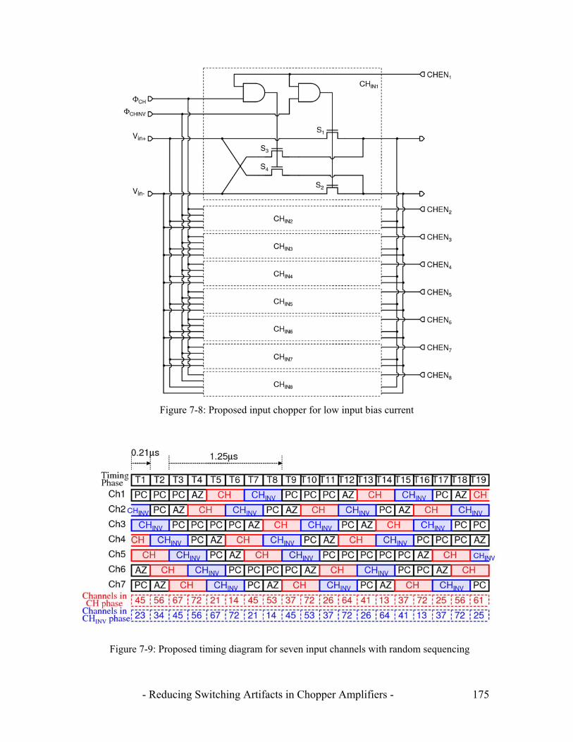
- Reducing Switching Artifacts in Chopper Amplifiers - 175
Figure 7-8: Proposed input chopper for low input bias current
Figure 7-9: Proposed timing diagram for seven input channels with random sequencing
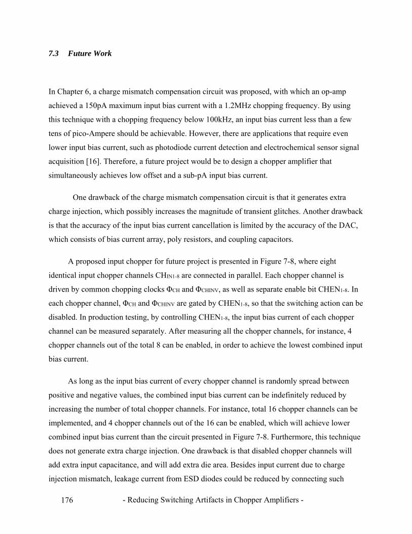
- Reducing Switching Artifacts in Chopper Amplifiers - 176
7.3 Future Work
In Chapter 6, a charge mismatch compensation circuit was proposed, with which an op-amp
achieved a 150pA maximum input bias current with a 1.2MHz chopping frequency. By using
this technique with a chopping frequency below 100kHz, an input bias current less than a few
tens of pico-Ampere should be achievable. However, there are applications that require even
lower input bias current, such as photodiode current detection and electrochemical sensor signal
acquisition [16]. Therefore, a future project would be to design a chopper amplifier that
simultaneously achieves low offset and a sub-pA input bias current.
One drawback of the charge mismatch compensation circuit is that it generates extra
charge injection, which possibly increases the magnitude of transient glitches. Another drawback
is that the accuracy of the input bias current cancellation is limited by the accuracy of the DAC,
which consists of bias current array, poly resistors, and coupling capacitors.
A proposed input chopper for future project is presented in Figure 7-8, where eight
identical input chopper channels CHIN1-8 are connected in parallel. Each chopper channel is
driven by common chopping clocks ΦCH and ΦCHINV, as well as separate enable bit CHEN1-8. In
each chopper channel, ΦCH and ΦCHINV are gated by CHEN1-8, so that the switching action can be
disabled. In production testing, by controlling CHEN1-8, the input bias current of each chopper
channel can be measured separately. After measuring all the chopper channels, for instance, 4
chopper channels out of the total 8 can be enabled, in order to achieve the lowest combined input
bias current.
As long as the input bias current of every chopper channel is randomly spread between
positive and negative values, the combined input bias current can be indefinitely reduced by
increasing the number of total chopper channels. For instance, total 16 chopper channels can be
implemented, and 4 chopper channels out of the 16 can be enabled, which will achieve lower
combined input bias current than the circuit presented in Figure 7-8. Furthermore, this technique
does not generate extra charge injection. One drawback is that disabled chopper channels will
add extra input capacitance, and will add extra die area. Besides input current due to charge
injection mismatch, leakage current from ESD diodes could be reduced by connecting such

- Reducing Switching Artifacts in Chopper Amplifiers - 177
diodes to the buffered input voltage, instead of supply voltages [17].
Another future project would be to further reduce the spectral peak associated with
transient glitches. In the design of Chapter 6, the majority of the glitch energy was pushed up to
4.8MHz, by driving six parallel input channels with 800kHz interleaved clocks. However, there
is still residual energy left at 800kHz, because, due to channel-channel mismatch, one input
channel would still generate a large transient glitch which would then occur every 1.25µs
(800kHz frequency).
A proposed technique for a future project would be to randomly sequence the phase of
every channel, rather than to sequence them with a fixed order. Figure 7-9 presents its proposed
timing diagram for seven input channels (Ch1-7), which contains one additional channel
compared to the circuit in Chapter 6. Similar to the timing diagram presented in Figure 6-5 (b),
each channel goes through pre-charge PC, auto-zero AZ, chopping CH, and inverting-chop
CHINV phases. With one additional channel, total two channels are in the PC phase in one timing
phase. Then, in the next timing phase, one channel out of the two is randomly selected to be
advanced to the AZ phase, while the other channel stays in the PC phase. For instance, in the
timing phase T1, Ch1 and Ch7 are in the PC phase. In the next timing phase T2, Ch7 is selected to
be advanced to the AZ phase, Ch1 stays in the PC phase, and Ch2 is advanced to the PC phase.
As in the Chapter 6 design, two channels are in the CH phase and other two channels are in
the CHINV phase at a time (total four channels are in the signal path), so that the overall amplifier
will achieve the same low frequency noise PSD and signal bandwidth specifications. On the
other hand, the combination of those four channels will be different after a period of 1.25µs, so
that a fixed-amplitude transient glitch will not repeat every 1.25µs. For instance, while Ch6 and
Ch7 are in the CH phase in T3, Ch3 and Ch7 are in the CH phase in T9 (1.25µs later).
Consequently, the residual spectral peak at 800kHz will be spread out in the frequency domain.
One drawback of this proposed technique is the additional current consumption and die area for
one extra input channel.

- Reducing Switching Artifacts in Chopper Amplifiers - 178
7.4 Original Contributions
The invention of the auto-correction feedback (ACFB) loop (Chapter 4)
Full analysis of the ACFB loop (Chapter 4)
The invention of a frequency compensation technique using a current attenuator and a
dummy differential output (Chapter 5)
The invention of an adaptive clock boosting technique in an input chopper (Chapter 5)
The realization of a capacitively-coupled auto-zeroed and chopped transconductor
(Chapter 6)
The realization of a multi-channel auto-zeroed and chopped transconductor with
interleaved clocks (Chapter 6)
The invention of input bias current trimming using an on-chip charge mismatch
compensation circuit (Chapter 6)
A comparison of the performance of different switching-artifact reduction techniques
(Chapter 7)
- Reducing Switching Artifacts in Chopper Amplifiers - 179
7.5 References
[1] Y. Kusuda, “Auto Correction Feedback for Ripple Suppression in a Chopper Amplifier”,
IEEE J. Solid-State Circuits, vol. 45, no. 8, pp. 1436-1445, Aug. 2010.
[2] Y. Kusuda, “A 5.9nV/√Hz Chopper Operational Amplifier with 0.78V Maximum Offset
and 28.3nV/C° Offset Drift”, IEEE ISSCC Dig. Tech. Papers, pp. 242-243, Feb. 2011.
[3] Y. Kusuda, “A 60 V Auto-Zero and Chopper Operational Amplifier With 800 kHz
Interleaved Clocks and Input Bias Current Trimming”, IEEE J. Solid-State Circuits, vol. 50, no.
12, pp. 2804-2813, Dec. 2015.
[4] A. T. K. Tang, “A 3V-Offset Operational Amplifier with 20nV/√Hz Input Noise PSD at DC
Employing both Chopping and Autozeroing”, IEEE ISSCC Dig. Tech. Papers, pp. 362-387, Feb.
2002.
[5] M. Kejariwal, P. Ammisetti, and A. Thomsen, “A 250+dB open loop gain feedforward
compensated high precision operational amplifier”, Proc. of IEEE ESSCIRC, pp. 187-190, Sept.
2002.
[6] J. F. Witte, K. A. A. Makinwa, and J. H. Huijsing, “A CMOS Chopper Offset-Stabilized
Opamp”, IEEE J. Solid-State Circuits, vol. 42, no. 7, pp. 1529-1535, July 2007.
[7] Q. Fan, J. H. Huijsing, and K.A.A. Makinwa, “A 21 nV/√Hz Chopper-Stabilized Multi-Path
Current-Feedback Instrumentation Amplifier With 2 µV Offset”, IEEE J. Solid-State Circuits,
vol. 47, no. 2, pp. 464-475, Feb. 2012.
[8] Texas Instruments, “OPA378 Datasheet”, Mar. 2006, Accessed on March 2018, [Online]
Available: <http://www.ti.com/lit/gpn/opa378>.
[9] Texas Instruments, “LMP2021 Datasheet”, Sept. 2009, Accessed on March 2018, [Online]
Available: <http://www.ti.com/lit/ds/symlink/lmp2022.pdf>.
- Reducing Switching Artifacts in Chopper Amplifiers - 180
[10] Intersil Corporation, “ISL28134 Datasheet”, June 2011, Accessed on March 2018, [Online]
Available: <http://www.intersil.com/content/dam/Intersil/documents/isl2/isl28134.pdf>.
[11] Maxim Integrated, “MAX44250 Datasheet”, Oct. 2011, Accessed on March 2018, [Online]
Available: <http://datasheets.maximintegrated.com/en/ds/MAX44250-MAX44252.pdf>.
[12] Texas Instruments, “OPA2188 Data Sheet”, Aug. 2011, Accessed on March 2018, [Online]
Available: <http://www.ti.com/lit/ds/symlink/opa2188.pdf>.
[13] Maxim Integrated, “MAX44246 Data Sheet”, July 2012, Accessed on March 2018, [Online]
Available: <http://datasheets.maximintegrated.com/en/ds/MAX44241-MAX44246.pdf>.
[14] Analog Devices, “LTC2057HV Data Sheet”, Aug. 2013, Accessed on March 2018, [Online]
Available: <http://www.analog.com/media/en/technical-documentation/data-sheets/2057f.pdf>.
[15] V. Ivanov and M. Shaik, “A 10MHz-Bandwidth 4s-Large-Signal-Settling 6.5nV/√Hz-
Noise 2V-Offset Chopper Operational Amplifier”, IEEE ISSCC Dig. Tech. Papers, pp. 88-89,
Feb. 2016.
[16] CH Instruments, Inc., “Model 600E Series Electrochemical Analyzer/Workstation”,
Accessed on March 2018, [Online] Available: <http://www.chinstruments.com/chi600.shtml>.
[17] M. Coln, G. Carreau, and Y. Kusuda, “Guarded Electrical Overstress Protection Circuit”,
United States Patent, US8837099 B2, Issued Sept. 2014.
- Reducing Switching Artifacts in Chopper Amplifiers - 181
Summary
This thesis describes the theory, design, and implementation of chopper operational amplifiers
(op-amps) in CMOS integrated circuits (ICs). The chopping technique periodically corrects DC
errors of such op-amps, so that low 1/f noise and stable, microvolt-level offset can be achieved.
However, chopping causes switching artifacts at the amplifier’s output, e.g. up-modulated ripple
and glitches, which are usually attenuated by low-pass filtering. Therefore, chopper op-amps
have mainly been limited to low frequency applications. In this thesis, advanced circuit
techniques are proposed to attenuate such switching artifacts without decreasing the usable signal
bandwidth, thus enabling the use of chopper op-amps in a broader range of applications. Three
chopper op-amps are designed, fabricated, and measured, so that the proposed techniques can be
evaluated and compared with those of the other state-of-the-art designs.
In Chapter 1, the advantages and disadvantages of CMOS chopper op-amps compared to
traditional bipolar op-amps are discussed. Without any offset cancellation techniques, CMOS op-
amps usually suffer from higher offset, temperature drift, and thermal and 1/f noise than bipolar
op-amps, given the same die size and current consumption. On the other hand, bipolar op-amps
are ruled out in many applications due to their manufacturing cost, high input bias current, and
difficulty of co-integration with CMOS ADCs and DACs. Additionally, digital logics and analog
switches can be easily implemented in CMOS process, which enables the use of dynamic offset
cancellation techniques such as auto-zeroing and chopping. These techniques can reduce
maximum offset and maximum offset drift of amplifiers to less than 10µV and 0.1µV/°C,
respectively, which can hardly be matched by bipolar op-amps.
In this chapter, traditional applications of chopper op-amps in sensor signal conditioning
and current sensing are reviewed. In such applications, signal frequencies are relatively low and
so switching artifacts can be attenuated by low-pass filtering. Signal source impedances are also
low, so that some input bias current can be tolerated. Next, newer applications of chopper op-
amps are reviewed, such as in DAC buffers and industrial process control, in which signal
frequencies are too high for the use of low-pass filtering to suppress switching artifacts. In
certain applications, e.g. biomedical sensing, source impedances can be quite high, and so input
- Reducing Switching Artifacts in Chopper Amplifiers - 182
bias currents must be less than 100pA.
In Chapter 2, in addition to the chopping technique, other offset cancellation techniques—
offset trimming and auto-zeroing—are reviewed. Trimming only corrects offset at post-
production test, and thus still results in high offset drift and 1/f noise. Like chopping, auto-
zeroing periodically corrects offset, and therefore effectively reduces offset drift and 1/f noise as
well. However, auto-zeroing introduces some dead time, during which the offset is sampled and
the op-amp is unavailable for signal amplification. To achieve continuous-time amplification, at
least two input channels are required. Moreover, sampling the offset causes high frequency noise
folding, and thus results in an in-band noise PSD that is higher than the initial thermal noise
floor. Chopping, on the other hand, is a frequency modulation technique which neither involves
sampling nor introduces noise folding, so that the resulting in-band noise PSD is only slightly
higher than the initial thermal noise floor. Therefore, chopping can achieve both low offset and
low in-band noise PSD in a more power efficient manner than auto-zeroing.
AC and DC errors caused by the switching artifacts in chopper amplifiers are then
reviewed, including up-modulated ripple, glitches caused by charge injection, residual offset, and
input bias current. Additionally, design trade-offs related to these errors are explained. AC
switching artifacts―ripple and glitches―can be pushed toward higher frequencies by increasing
the chopping frequency. However, this increases the amount of charge injection mismatch
generated per unit of time, thus increasing DC errors such as residual offset and input bias
current. These DC errors also increase when wider input switches are used for lower on-
resistance and hence, lower thermal noise. Due to these trade-offs, previous chopper op-amps
(with chopping frequencies above 200kHz and noise PSDs less than 20nV/√Hz) could only
achieve residual input offsets and input bias currents greater than 10µV and 500pA, respectively.
In Chapter 3, three known techniques to reduce the DC errors are reviewed. One technique
employs a band-pass filter (BPF) to attenuate the glitches caused by charge injection mismatch,
before they are down-modulated and turned into DC errors. However, this requires active
circuitry to realize the BPF and thus is not power efficient. Another technique is to use a down-
modulation clock with a dead-band, so that the amplifier’s output is frozen until the glitches
settle. However, the amplifier is unavailable during the dead-band, which decreases its effective
- Reducing Switching Artifacts in Chopper Amplifiers - 183
gain and increases its input referred noise PSD. Yet another technique, called nested chopping,
employs a combination of fast and slow chopping. In this case, while amplifier offset and 1/f
noise are up-modulated by the fast chopping, the resulting DC errors are up-modulated by the
slow chopping. However, it results in a high noise PSD at the slow chopping frequency, which
limits the usable signal bandwidth.
Additionally, known ripple reduction techniques are also reviewed. An active filter can
be used to attenuate up-modulated ripple at the cost of extra current. Alternatively, a passive
switched-capacitor notch filter (SC-NF) can be used, although the up-modulated ripple will still
be present at its input. A relatively high chopping frequency is then required to ensure that this
ripple does not saturate the output of the input transconductor. To avoid such ripple, the initial
offset at the output of an input transconductor can be blocked by a correlated double sampling
(CDS) or an RC high-pass filter. However, the gain of the input transconductor must be limited
to ensure that its output is not saturated by the initial offset. With these filtering techniques, the
up-modulated ripple and/or initial offset still remain, which restricts and/or complicates the
design.
Therefore, the preferred approach is to cancel the initial offset that would otherwise turn
into output ripple. One way of doing this is by trimming the initial offset, although this, and the
associated ripple, will then drift with temperature. Instead, the initial offset can be auto-zeroed,
and the resulting high in-band noise PSD can be up-modulated by chopping. However, to
achieve continuous-time amplification, this requires an additional input channel that consumes
extra current and die area. Another technique is to use a ripple reduction loop (RRL) that
continuously detects the ripple and uses this information to cancel the initial offset. The notch
created by the RRL can be buried by adding a high frequency path (HFP). Furthermore, instead
of using a continuous-time filter in its feedback path, the RRL can also be realized digitally with
a ripple-sensing comparator and a DAC in a more area efficient manner, although higher digital
resolution is required to reduce the residual ripple.
In Chapter 4, a ripple reduction technique called auto-correction feedback (ACFB) is
proposed, which also continuously detects the ripple and uses this information to cancel the
initial offset. In contrast to the RRL, ACFB senses the ripple at the output of the output chopper,
- Reducing Switching Artifacts in Chopper Amplifiers - 184
and employs a switched-capacitor notch-filter (SC-NF) in its feedback path to selectively reduce
the initial offset without affecting desired DC and low frequency signals. Since the SC-NF is not
used in the main signal path, its clock frequency can be set relatively low, which will reduce the
residual offset and input bias current. However, its ripple sensing point is also the input of the
subsequent transconductor stage, which decreases the loop gain of the ACFB, and hence its
ripple reduction capability. Like the RRL, the ACFB requires a high frequency path to bury the
notch and to maintain the stability.
The proposed ACFB has been implemented in a stand-alone chopper op-amp that targets
portable applications. This only draws 13µA from a 1.8V to 5.5V supply and occupies a
0.64mm2 die area. Compared to a previous ripple reduction technique that used a SC-NF in the
main signal path, ACFB requires sensing and nulling transconductors, although they only
consume 5% of the op-amp’s supply current. Furthermore, the use of ACFB allows the chopping
frequency to be set to a relatively low 50kHz, thus only resulting in a 50pA maximum input bias
current.
In Chapter 5, a chopper op-amp that achieves a 5.6nV/√Hz noise PSD is presented, as
well as circuit techniques to relax the design trade-offs between noise PSD and other
specifications. With the proposed frequency compensation technique, based on a current
attenuator and a dummy differential output, the overall op-amp only draws 1.4mA from a 2.1V
to 5.5V supply and occupies a die area of 1.26mm2. In contrast to the design in the previous
chapter, an active integrator is employed in the ACFB to boost its loop gain, thus suppressing its
own residual offset, and hence the residual ripple. On the other hand, the active integrator also
contributes to the sampled noise in the SC-NF, and hence to the up-modulated noise PSD at the
chopping frequency.
In general, residual offset tends to increase when targeting lower noise PSD, due to
increased charge injection mismatch from the wider input switches required for low thermal
noise. Moreover, when the input chopping clocks have a fixed amplitude, extra wide switches
are required to compensate for the lower overdrive voltages associated with mid-range input
common-mode voltages. To overcome this problem, an adaptive clock boosting technique is
proposed to drive NMOS input switches, so that charge injection mismatch is minimized and
- Reducing Switching Artifacts in Chopper Amplifiers - 185
independent of changes in the supply and input common-mode voltages. As a result, 0.5µV
maximum offset and 0.015µV/°C maximum offset drift are achieved over the op-amp’s entire
rail-to-rail input common-mode range and a –40°C to 125°C temperature range.
In Chapter 6, a chopper op-amp is realized primarily for industrial applications, where
wide supply and input common-mode voltage ranges are required as well as wide signal
bandwidth. To achieve a 4.5V to 60V supply range, the op-amp is realized in a 0.18µm CMOS
process augmented by 5V CMOS and 60V DMOS transistors. The capacitively-coupled input
transconductor is pre-charged, auto-zeroed, and then chopped to achieve low offset, low output
ripple, and wide input common-mode voltage range without creating a notch in the signal
transfer function. The initial offset of the input transconductor is suppressed by a dual coarse-
fine auto-zero technique without relying on extra gain stages in the auto-zero loop, thus avoiding
excess sampled noise. To achieve continuous-time amplification, the whole input transconductor
consists of six parallel channels, four of which amplify the input signal at a time. This reduces
the input transconductance and switch width required in each channel. Consequently, to achieve
the same in-band noise PSD, all six input transconductors only consume 1.5 more current than a
non-auto-zeroed input transconductor. Moreover, due to the smaller switches, smaller glitches
are produced per channel, thus pushing the PSD peak to 4.8MHz when each channel is driven by
interleaved 800kHz clocks. Furthermore, an on-chip charge mismatch compensation circuit is
employed to reduce the maximum input bias current from 1.5nA down to 150pA in post-
production trimming.
In Chapter 7, the performances of the realized three chopper op-amps are compared with
each other and with the other state-of-the-art. In later designs, the proposed techniques allow
higher chopping frequencies to be used, while DC errors either improve or remain competitive.
In the op-amps of Chapter 5 and 6, the input switches are driven by local clock supply voltages
that track their input common-mode voltage, thus reducing their charge injection mismatch and
hence residual offset. In the op-amp of Chapter 6, the charge injection mismatch is further
reduced by an on-chip charge mismatch compensation circuit in post-production trimming.
Consequently, the op-amps in Chapter 5 and 6 both achieve less residual offset and less input
bias current than other comparable designs, i.e. with less than 20nV/√Hz noise PSDs and
chopping frequencies greater than 200kHz. In the op-amp of Chapter 4, the maximum noise PSD

- Reducing Switching Artifacts in Chopper Amplifiers - 186
peak at the chopping frequency is 820nV/√Hz, which is dominated by the ACFB’s residual
offset due to its finite loop gain. In Chapter 5, an active integrator is employed in the ACFB to
boost its loop gain. However, the sampled noise in the SC-NF is increased by the active
integrator, which dominates the maximum noise PSD peak of 62nV/√Hz. In Chapter 6, the
residual offset in the auto-zero loop is suppressed by the dual coarse-fine auto-zero technique
without relying on additional gain stages, thus avoiding excess sampled noise and achieving the
maximum noise PSD peak of 13.5nV/√Hz. Moreover, in the Chapter 6 design, the noise PSD
peak due to glitches is pushed up to 4.8MHz by the clock interleaving technique.
- Reducing Switching Artifacts in Chopper Amplifiers - 187
Samenvatting
Dit proefschrift beschrijft de theorie, het ontwerp en de implementatie van chopper operationele
versterkers (op-amps) in CMOS geïntegreerde schakelingen (ICs). De chopping techniek
corrigeert periodiek DC fouten van zulke op-amps, zodat lage 1/f ruis en stabiele, microvolt-
niveau offset bereikt kan worden. Chopping veroorzaakt echter schakelartefacten op de uitgang
van de versterker, zoals omhoog-gemoduleerde rimpel en glitches, die meestal worden
onderdrukt door laagdoorlaatfilters. Daardoor is het gebruik van chopper op-amps vooral beperkt
tot laagfrequente toepassingen. In dit proefschrift worden geavanceerde circuittechnieken
voorgesteld om deze schakelartefacten te onderdrukken, zonder daarbij de bruikbare
signaalbandbreedte te verminderen. Hierdoor wordt het gebruik van chopper op-amps in een
breder scala van toepassingen mogelijk. Drie chopper op-amps zijn ontworpen, gefabriceerd en
gemeten, zodat de voorgestelde technieken geëvalueerd en vergeleken kunnen worden met
andere state-of-the-art ontwerpen.
In Hoofdstuk 1 worden de voor- en nadelen van CMOS chopper op-amps in vergelijking
met traditionele bipolaire op-amps besproken. Zonder enige offset wegwerk technieken, hebben
CMOS op-amps last van hogere offset, temperatuur verschuivingen en thermische en 1/f ruis dan
bipolaire op-amps, gegeven een vergelijkbare chip grootte en stroomverbruik. Aan de ander kant
zijn bipolaire op-amps in veel toepassingen uitgesloten vanwege de hoge productiekosten, hoge
ingangs-biasstroom en moeilijke integratie met CMOS ADCs en DACs. Daarnaast zijn digitale
logica en analoge schakelaars makkelijk implementeerbaar in CMOS processen, wat het gebruik
van dynamische offset compensatie technieken, zoals auto-zeroing en chopping, mogelijk maakt.
Deze technieken kunnen de maximale offset en maximale offset drift van versterkers reduceren
tot respectievelijk minder dan 10µV en 0.1µV/°C, welke moeilijk geëvenaard kunnen worden
door bipolaire op-amps.
In dit hoofdstuk worden de traditionele toepassingen van chopper op-amps in sensor
signaalconditionering en stroommetingen besproken. In dergelijke toepassingen zijn
signaalfrequenties relatief laag en kunnen schakelartefacten dus verminderd worden door
laagdoorlaat filtering. Signaalbronimpedanties zijn ook laag, waardoor wat ingangsstroom

- Reducing Switching Artifacts in Chopper Amplifiers - 188
getolereerd kan worden. Daarna worden nieuwe toepassingen van chopper op-amps besproken,
zoals DAC buffers en industriële procescontrole, waarin signaalfrequenties te hoog zijn voor het
gebruik van laagdoorlaatfilters om schakelartefacten te verminderen. In bepaalde toepassingen,
zoals biomedische detectie, kunnen bronimpedanties vrij hoog zijn en moet de ingangs-bias-
stroom dus lager zijn dan 100pA.
In Hoofdstuk 2 word naast de chopping techniek, de andere offset reductie technieken -
offset trimmen en auto-zeroing - besproken. Trimmen corrigeert offset alleen tijdens de na-
productietest en zal dus nog steeds resulteren in een hoge offset drift en 1/f ruis. Net als chopping
corrigeert auto-zeroing de offset periodiek en zorgt daardoor ook voor een effectief lagere offset
drift en 1/f ruis. Auto-zeroing introduceert echter wat dode tijd, gedurende welke de offset
bemonsterd wordt en de op-amp niet beschikbaar is voor versterking. Om tijd-continue
versterking te bereiken zijn tenminste twee ingangskanalen nodig. Daarnaast zorgt het
bemonsteren van de offset voor het terugvouwen van hoogfrequente ruis en dit resulteert in een
in-band ruis PSD die hoger is dan het initiële thermische ruis niveau. Aan de andere kant is
chopping een frequentiemodulatie techniek waarbij geen sprake is van bemonstering of het
terugvouwen van ruis. Hierdoor is de resulterende in-band ruis PSD slecht licht verhoogd ten
opzichte van het initiële thermische ruis niveau. Daarom kan chopping zowel lage offset als lage
in-band ruis PSD bereiken op een meer vermogens-efficiënte manier dan auto-zeroing.
AC en DC fouten veroorzaakt door de schakelartefacten in chopper versterkers worden
vervolgens besproken, inclusief omhoog-gemoduleerd rimpel, glitches veroorzaakt door
ladingsinjectie, overgebleven offset en ingangs-biasstroom. Daarnaast worden ontwerp-
compromissen gerelateerd aan deze fouten besproken. AC schakelartefacten – rimpel en glitches
– kunnen naar hogere frequenties gedrukt worden door een hogere chopfrequentie te gebruiken.
Echter verhoogt dit ook de hoeveelheid mismatch van de ladingsinjectie gegenereerd per
tijdseenheid, wat dus de DC fouten zoals overgebleven offset en ingangs-biasstroom verhoogd.
Deze DC fouten worden ook groter als bredere ingangsschakelaars gebruikt worden voor lagere
aan-weerstand en dus lagere thermische ruis. Door deze compromissen, konden eerder chopper
op-amps (met chopfrequenties boven 200kHz en ruis PSDs lager dan 20nV/√Hz) alleen
overgebleven ingangs-offset en ingangs-biasstroom bereiken respectievelijk groter dan 10µV en
500pA.

- Reducing Switching Artifacts in Chopper Amplifiers - 189
In Hoofdstuk 3 worden drie bekende technieken om DC fouten te verminderen
besproken. Een techniek gebruikt een banddoorlaatfilter (BPF) om glitches veroorzaakt door de
mismatch van ladingsinjectie te verminderen, voordat deze omlaag-gemoduleerd worden in DC
fouten. Dit vereist echter actieve circuits om de BPF te realiseren en is dus niet vermogens-
efficiënt. Een andere techniek is om een klok voor omlaag-modulatie te gebruiken met een dode-
tijd, zodat de uitgang van de versterker wordt vastgezet totdat de glitches tot rust zijn gekomen.
De versterker is echter niet beschikbaar gedurende de dode-tijd, wat de effectieve versterking
verlaagt en de ingangsruis PSD verhoogt. Een andere techniek, genaamd nested chopping,
gebruikt een combinatie van snel en langzaam choppen. In dit geval wordt de versterker zijn
offset en 1/f ruis omhoog gemoduleerd door snel te choppen, terwijl de resulterend DC fouten
omhoog gemoduleerd worden door langzaam te choppen. Dit resulteert echter in een hogere ruis
PSD bij de lage chopfrequentie, wat de bruikbare bandbreedte beperkt.
Daarnaast worden bekende rimpel reductie technieken besproken. Een actief filter kan
gebruikt worden om omhoog-gemoduleerde rimpel te onderdrukken, ten kosten van extra
stroom. Als alternatief kan een passief geschakelde-capaciteit bandstopfilter (SC-NF) worden
gebruikt, hoewel de omhoog-gemoduleerde rimpel nog steeds op de ingang aanwezig blijft. Een
relatief hoge chopfrequentie is dan noodzakelijk om te zorgen dat deze rimpel de uitgang van de
ingangstransconductor niet verzadigt. Om dit soort rimpel te voorkomen, kan de initiële offset op
de uitgang van de ingangstransconductor geblokkeerd worden door gecorreleerde dubbele
bemonstering (CDS) of een RC hoogdoorlaatfilter. De versterking van de ingangstransconductor
moet echter gelimiteerd zijn, om te zorgen dat de uitgang niet verzadigt wordt door de initiële
offset. Met deze filtertechnieken blijven omhoog-gemoduleerd rimpel en/of initiële offset nog
over, wat het ontwerp beperkt en/of compliceert.
Daarom wordt de voorkeur gegeven aan een benadering waarbij de initiële offset wordt
opgeheven, die anders tot uitgangs-rimpel zou leiden. Een manier om dit te doen is door de
initiële offset te trimmen, al zal deze en de bijbehorende rimpel dan verschuiven met
temperatuur. In plaats daarvan kan de initiële offset geauto-zeroed worden en kan de resulterende
hoge in-band ruis PSD omhoog-gemoduleerd worden door te choppen. Echter, om tijd-continue
versterking te verkrijgen, vereist dit een additioneel ingangskanaal die extra stroom en
oppervlakte consumeert. Een andere techniek is om een rimpel reductie lus (RRL) te gebruiken
- Reducing Switching Artifacts in Chopper Amplifiers - 190
die continu de rimpel detecteert en deze informatie gebruikt om de initiële offset op te heffen. De
bandstop gecreëerd door de RRL kan bedekt worden door een hoogfrequentpad (HFP) toe te
voegen. Daarnaast kan in plaats van het gebruik van een tijd-continu filter in het terugkoppelpad,
de RRL ook digitaal gerealiseerd worden met een rimpel-voel comparator en een DAC in een
oppervlak effectievere manier, al is een hoge digitale resolutie dan noodzakelijk om de
overgebleven rimpel te reduceren.
In Hoofdstuk 4 wordt een rimpel reductie techniek genaamd auto-correctie
terugkoppeling (ACFB) voorgesteld, die ook continu de rimpel detecteert en deze informatie
gebruikt om de initiële offset op te heffen. In tegenstelling tot de RRL detecteert ACFB de
rimpel op de uitgang van de uitgangschopper en gebruikt het een geschakelde-capaciteit
bandstopfilter in zijn terugkoppelpad om de initiële offset selectief te reduceren, zonder de
gewilde DC en laagfrequente signalen te beïnvloeden. Aangezien de SC-NF niet wordt gebruikt
in het hoofdsignaalpad, kan de klokfrequentie ervan relatief laag worden ingesteld, wat de
overgebleven offset en de ingangs-biasstroom verlaagt. Het rimpel uitleespunt is echter ook de
ingang van de volgende transconductietrap, wat de lusversterking van de ACFB verlaagt en
daarmee zijn vermogen om de rimpel te reduceren. Net als de RRL heeft de ACFB een
hoogfrequentpad nodig om de bandstop karakteristiek te verbergen en om stabiliteit te behouden.
De voorgestelde ACFB is geïmplementeerd in een opzichzelfstaande chopper op-amp
voor gebruik in mobiele applicaties. Het gebruikt slechts 13µA van een 1.8V tot 5.5V voeding en
neemt een oppervlak vaan 0.64mm2 in beslag. In vergelijk met een eerdere rimpel reductie
techniek die een SC-NF gebruikt in het hoofdsignaalpad, vraagt ACFB voel- en
opheftransconductors, alhoewel deze slechts 5% van de op-amps voedingsstroom gebruiken.
Verder staat het gebruik van ACFB toe dat de chopfrequentie op een relatief lage 50kHz word
ingesteld, wat resulteert in een maximale ingangs-biasstroom van slechts 50pA.
In Hoofdstuk 5 wordt een chopper op-amp gepresenteerd die een 5.6nV/√Hz ruis PSD
bereikt, als mede circuittechnieken om de ontwerpcompromissen tussen ruis PSD en ander
specificaties te verzachten. Met de voorgestelde frequentie-compensatietechniek, gebaseerd op
een stroomverzwakker en een dummy differentiëleuitgang, gebruikt de gehele op-amp slechts
1.4mA van een 2.1V tot 5.5V voeding en neemt slechts 1.26 mm2 in. In tegenstelling tot het

- Reducing Switching Artifacts in Chopper Amplifiers - 191
ontwerp uit het vorige hoofdstuk wordt een actieve integrator gebruikt in de ACFB, om de
lusversterking te verhogen, wat de eigen overgebleven offset onderdrukt en daarmee de
overgebleven rimpel. Aan de andere kant draagt de actieve integrator ook bij aan de gesampelde
ruis in de SC-NF en daardoor de omhoog-gemoduleerd ruis PSD op de chopfrequentie.
In het algemeen leidt een streven tot lagere ruis PSD tot hogere overgebleven offset, door
de toegenomen ladingsinjectie van de bredere ingangsschakelaar die nodig zijn voor lage
thermische ruis. Daarnaast, als de ingangs-chopklokken een vaste amplitude hebben, zijn er extra
brede schakelaars nodig om te compenseren voor de lagere overstuurspanning, in relatie tot het
midden van het ingangs-common-mode spanningsbereik. Om dit probleem te overkomen, wordt
een adaptieve klok boost techniek voorgesteld om de NMOS ingangsschakelaars aan te sturen,
zodat de mismatch van de ladingsinjectie geminimaliseerd wordt en onafhankelijk is van
veranderingen in de voedings- en ingangs-common-mode spanning. Dit resulteert in een
maximale offset en offset drift van respectievelijk 0.5µV en 0.015 µV/°C, over het gehele rail-to-
rail ingangs-common-mode bereik van de op-amp en over een temperatuurbereik van –40°C tot
125°C.
In Hoofdstuk 6 is een chopper op-amp gerealiseerd primair voor industriële toepassingen,
waar grote voedings- en ingangs-common-mode spanningsbereik vereist zijn alsmede een grote
signaalbandbreedte. Om een 4.5V tot 60V voedingsbereik te verkrijgen, is deze op-amp
gerealiseerd in een 0.18µm CMOS proces aangevuld met 5V CMOS en 60V DMOS transistoren.
De capacitief-gekoppelde ingangstransconductor is voor-geladen, geauto-zeroed en vervolgens
gechopped om lage offset, uitgangsrimpel en een groot ingangs-common-mode spanningsbereik
te verkrijgen zonder een bandstop in de signaaloverdracht te krijgen. De initiële offset van de
ingangstransconductor wordt onderdrukt door een dubbele grof-fijn auto-zero techniek zonder
gebruikt te maken van extra versterkingstrappen in de auto-zero lus, wat overmatig bemonsterde
ruis voorkomt. Om tijd-continue versterking te verkrijgen bestaat de ingangstransconductor uit
zes parallelle kanalen, waarvan vier per keer het ingangssignaal versterken. Dit reduceert de
benodigde ingangstransconductantie en breedte van de ingangsschakelaars per kanaal. Daardoor
consumeren de zes ingangstransconductors slechts 1.5 keer meer stroom dan een niet
geautozeroede ingangstransconductor, om dezelfde PSD van de in-band ruis te bereiken.
Bovendien produceren de kleinere schakelaars kleinere glitches per kanaal, wat de PSD piek naar
- Reducing Switching Artifacts in Chopper Amplifiers - 192
4.8MHz duwt wanneer ieder kanaal wordt aangestuurd door een 800kHz interleaved klok.
Daarnaast wordt een op-de-chip compensatie circuit gebruikt voor de mismatch van de
ladingsinjectie. Dit reduceert de maximale ingangs-biasstroom van 1.5nA naar 150pA in een na-
productie trim.
In Hoofdstuk 7 worden de prestaties van de drie gerealiseerde chopper op-amps
vergeleken met elkaar en met de rest van de state-of-the-art. In de latere ontwerpen staat de
voorgestelde techniek het gebruik van hogere chopfrequenties toe, terwijl DC fouten verbeterd
worden of hetzelfde blijven. In de op-amps van Hoofdstuk 5 en 6 worden de ingangsschakelaars
aangestuurd door een voedingsspanning die de ingangs-common-mode spanning volgt. Dit
vermindert de mismatch van de ladingsinjectie en verlaagt daarmee ook de overgebleven offset.
In de op-amp uit Hoofdstuk 6 wordt de mismatch van de ladingsinjectie verder gereduceerd door
het gebruikt van een op-de-chip compensatiecircuit voor de mismatch van de ladingsinjectie in
een na-productie trim. Daardoor behalen beide op-amps in Hoofdstuk 5 en 6 lagere overgebleven
offset en lagere ingangs-biasstroom dan andere vergelijkbare ontwerpen, met minder dan
20nV/√Hz ruis PSDs en een chopfrequentie hoger dan 200kHz. In de op-amp uit Hoofdstuk 4 is
de maximale ruis PSD piek 820nV/√Hz bij de chopfrequentie. Dit wordt gedomineerd door de
overgebleven offset veroorzaakt door de beperkte lusversterking van de ACFB. In Hoofdstuk 5
wordt een actieve integrator gebruikt in de ACFB om de lusversterking te verhogen. De
bemonsterde ruis in de SC-NF wordt echter verhoogd door de actieve integrator, wat de
maximale ruis PSD piek van 62nV/√Hz domineert. In Hoofdstuk 6 wordt de overgebleven offset
in de auto-zero lus onderdrukt door een dubbele grof-fijn auto-zero techniek, zonder gebruikt te
maken van extra versterkingstrappen, wat overmatig gesampelde ruis voorkomt en een maximale
ruis PSD piek van 13.5nV/√Hz oplevert. Daarnaast, in het ontwerp van Hoofdstuk 6, is de ruis
PSD piek als gevolg van de glitches omhoog geduwd naar 4.8MHz door een klok interleave
techniek.
- Reducing Switching Artifacts in Chopper Amplifiers - 193
List of publications
Conference Papers
Y. Kusuda, “Auto Correction Feedback for ripple suppression in a chopper amplifier”, IEEE
CICC Dig. Tech. Papers, pp. 573-576, Sept. 2009.
Y. Kusuda, “A 5.9nV/√Hz Chopper Operational Amplifier with 0.78V Maximum Offset and
28.3nV/C° Offset Drift”, IEEE ISSCC Dig. Tech. Papers, pp. 242-243, Feb. 2011.
Y. Kusuda, “A 60V Auto-zero and Chopper Operational Amplifier with 800kHz Interleaved
Clocks and Input Bias Current Trimming”, IEEE ISSCC Dig. Tech. Papers, pp. 88-89, Feb.
2015.
Journals
Y. Kusuda, “Auto Correction Feedback for Ripple Suppression in a Chopper Amplifier”, IEEE J.
Solid-State Circuits, vol. 45, no. 8, pp. 1436-1445, Aug. 2010.
Y. Kusuda, “A 60 V Auto-Zero and Chopper Operational Amplifier With 800 kHz Interleaved
Clocks and Input Bias Current Trimming”, IEEE J. Solid-State Circuits, vol. 50, no. 12, pp.
2804-2813, Dec. 2015.
Y. Kusuda, “A 5.6 nV/√Hz Chopper Operational Amplifier Achieving a 0.5 V Maximum
Offset Over Rail-to-Rail Input Range with Adaptive Clock Boosting Technique”, IEEE J. Solid-
State Circuits, vol. 51, no. 9, pp. 2119-2128, Sept. 2016.
Technical Articles
V. Wong and Y. Kusuda, “Zero-Drift Amplifiers: Now Easy to Use in High Precision Circuits”,
July 2015, Accessed on March 2018, [Online] Available:
<http://www.analog.com/library/analogdialogue/archives/49-07/Zero-Drift_Amplifiers.pdf>.
- Reducing Switching Artifacts in Chopper Amplifiers - 194
V. Wong and Y. Kusuda, “Zero-Drift Amplifiers: Now Easy to Use in High Precision Circuits”,
EDN NETWORK, Aug. 2015, Accessed on March 2018, [Online] Available:
<http://www.edn.com/design/analog/4440123/Zero-Drift-Amplifiers--Now-easy-to-use-in-high-
precision-circuits>.
Patents
Y. Kusuda and T. L. Botker, “Auto Correction Feedback Loop for Offset and Ripple Suppression
in a Chopper-Stabilized Amplifier”, United States Patent, US7764118 B2, Issued July 2010.
Y. Kusuda, “Low Power and Low Noise Switched Capacitor Integrator with Flexible Input
Common Mode Range”, United States Patent, US8125262 B2, Issued Feb. 2012.
G. Carreau, M. Coln, and Y. Kusuda, “Opportunistic Timing Control in Mixed-Signal System-
on-Chip Designs”, United States Patent, US8203357 B2, Issued June 2012.
Y. Kusuda, “Apparatus and Methods for Reducing Output Noise of a Single Channel”, United
States Patent, US8542066 B2, Issued Sept. 2013.
M. Coln, G. Carreau, and Y. Kusuda, “Correlated Double-Sampling Differencing within an
ADC”, United States Patent, US8754799 B2, Issued June 2014.
M. Coln, G. Carreau, and Y. Kusuda, “Guarded Electrical Overstress Protection Circuit”, United
States Patent, US8837099 B2, Issued Sept. 2014.
Y. Kusuda, G. Carreau, and M. Coln, “Apparatus and Methods for Reducing Common-Mode
Noise in an Imaging System”, United States Patent, US9123104 B2, Issued Sept. 2015.
Y. Kusuda, “Apparatus and Methods for Input Bias Current Reduction”, United States Patent,
US9246484 B2, Issued Jan. 2016.
Y. Kusuda, “Apparatus and Methods for Multi-Channel Autozero and Chopper Amplifiers”,
United States Patent, US9496833 B2, Issued Nov. 2016.

- Reducing Switching Artifacts in Chopper Amplifiers - 195
About the author
Yoshinori Kusuda received the B.S. degree in electrical and electronic engineering in 2002, and
M.S. degree in Physical Electronics in 2004, both from Tokyo Institute of Technology. Upon his
graduation in 2004, he joined the Japan Design Center of Analog Devices as an IC design
engineer. Since then, he has been with the same company, and is currently based in San Jose,
CA, U.S.A., working for the Linear and Precision Technology Group. He has been working for
precision CMOS analog designs, including stand-alone amplifiers and application specific
mixed-signal products. This has resulted in presentations and papers at IEEE conferences and
journals, as well as nine issued U.S. patents. Since August 2015, he has been registered as a
guest in the Electronic Instrumentation Laboratory of the TU Delft, pursuing his Ph.D. degree on
the subject of reducing switching artifacts in chopper amplifiers.

- Reducing Switching Artifacts in Chopper Amplifiers - 196

- Reducing Switching Artifacts in Chopper Amplifiers - 197
Acknowledgements
I am finally at this point writing the last few pages of the thesis. It was a wonderful and precious
opportunity for me to work on a series of chopper amplifier projects. Although there were many
tough challenges in the projects, I always enjoyed such challenges. The work described in this
thesis could not have been done without kind advices and dedicated support from many great
people in TU Delft and Analog Devices.
First, I would like to gratefully acknowledge my promoter, Professor Kofi Makinwa for
leading me to my PhD path. I first met him in his lecture at ISSCC 2007 about chopper amplifier,
when I was just about starting its research and design in Analog Devices. I was greatly impressed
with his deep knowledge as well as listener friendly lecture style. Even with my poor listening
skill at that time, I was able to learn from his every single slide and comment. Since then, I have
followed his research papers, and obtained his technical advices in conferences and through
emails. I learned a lot from him even before he became my promoter.
I was extremely excited when Kofi encouraged me to pursue my PhD under his
promotion, not only because this would give me the opportunity to receive an advanced degree,
but because I could learn from him more closely. His technical questions and suggestions were
always sharp, which motivated me and led me to the right direction. I would also acknowledge
his dedicated instructions on my thesis writing, while he must have had a lot of other work as a
professor and the department head. He often read my thesis over his weekend and provided
feedback. I learned from him not only about circuit design, but about how to present the work in
such a way that people understand and appreciate it. Such my experiences under him will be
tremendous benefit in my future career.
Second, I’d like to acknowledge Joyce Siemers, Karen van Busschbach, and other
secretaries in the Graduate School of TU Delft. Despite the geographic difference between the
Netherlands and California, the administrative procedure of my PhD project went smoothly

- Reducing Switching Artifacts in Chopper Amplifiers - 198
thanks to their kind support over the phone and email. I’d also acknowledge Sarah von Galambos
for reviewing and correcting my English writing, and Thije Rooijers for translating the summary
into Dutch.
Third, I’d like to acknowledge my managers in Analog Devices, who supervised and
supported my work. Tom Botker was my manager when I first started chopper amplifier design.
Despite the pressure from project schedule, he allowed me to spend extra time to try new ideas.
Patrick Fung was my great mentor as well as manager, and taught me how to be a good technical
leader in an engineering team. He trusted my design skill and provided me the opportunity to
work on a series of chopper amplifier projects. Art Kalb is my manager and Arie van Rhijn is
engineering director when I started writing my PhD thesis. They encouraged me to pursue PhD
degree and made it possible while I still work in Analog Devices.
Fourth, I’d like to acknowledge many other IC designers and technologists in Analog
Devices, who participated my design reviews and provided their technical insights. Their
feedback enhanced the technical quality of my design and raised the success rate of first silicon. I
also learned a lot from their design reviews and daily conversations with them.
Last but not least, I would like to gratefully acknowledge my project team members in
Analog Devices, who conducted mask layout, bench measurements, ATE testing, and reliability
testing. Over the three projects described in this thesis, I worked with approximately 20
engineers directly and probably with other 20 engineers or more indirectly. In every project, we
worked really hard to develop and evaluate such low offset and low noise amplifier. Without
their hard work, the circuit designs and techniques described in this thesis would not have been
proven.