department of information engineering357 operation amplifier the tail, large impedance gives high...
Post on 15-Jan-2016
220 views
TRANSCRIPT

1Department of Information Engineering
Operation amplifier
The tail,large impedancegives high CMRR
Mirror asactive load.High gain
Follower as buffer
amplifier
Push-pullclass B amp
2Department of Information Engineering
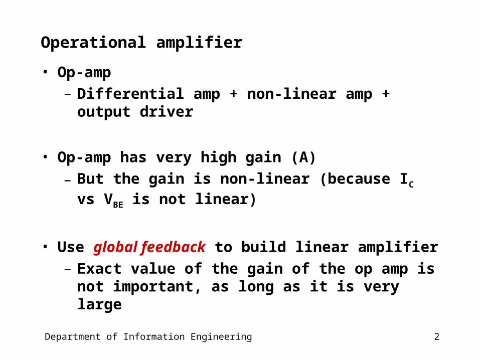
Operational amplifier
• Op-amp
– Differential amp + non-linear amp + output driver
• Op-amp has very high gain (A)
– But the gain is non-linear (because IC vs VBE is not linear)
• Use global feedback to build linear amplifier
– Exact value of the gain of the op amp is not important, as long as it is very large

3Department of Information Engineering
Feedback Op amp golden rules
Approximations:
1. Voltage difference between the two inputs is zero
2. Input draws no current
Why?
– VOUT = A VIN
– If VOUT is around 10V, A=10,000, then VIN ~ 1mV, voltage difference ~ 1mV (close to zero)
– FET draws virtually zero input current
VIN VOUT

4Department of Information Engineering
Gain of this amplifier?
V
1 2
2
1 1 2
2
1
( ) ( )
(assume opamp draws no input current)
( )
~ (assume A is very large)
OUT
OUT
IN OUT
IN
V A V V AV V V V
V V V V
R R
V AR
V AR R R
R
R

5Department of Information Engineering
An easier method
• Because A is so large that V ~ 0 (known as virtual earth)
V ~ 0
1 2
2
1
00 OUTIN
OUT
IN
VV
R R
V R
V R
6Department of Information Engineering
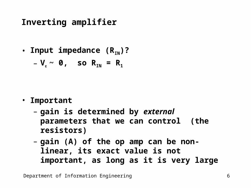
Inverting amplifier
• Input impedance (RIN)?
– V~ 0, so RIN = R1
• Important
– gain is determined by external parameters that we can control (the resistors)
– gain (A) of the op amp can be non-linear, its exact value is not important, as long as it is very large

7Department of Information Engineering
Negative feedback
• Feedback MUST be applied to the –ve terminal (–ve feedback), so that V~ 0 (IMPORTANT)
A) Works B) Doesn’t Work
8Department of Information Engineering
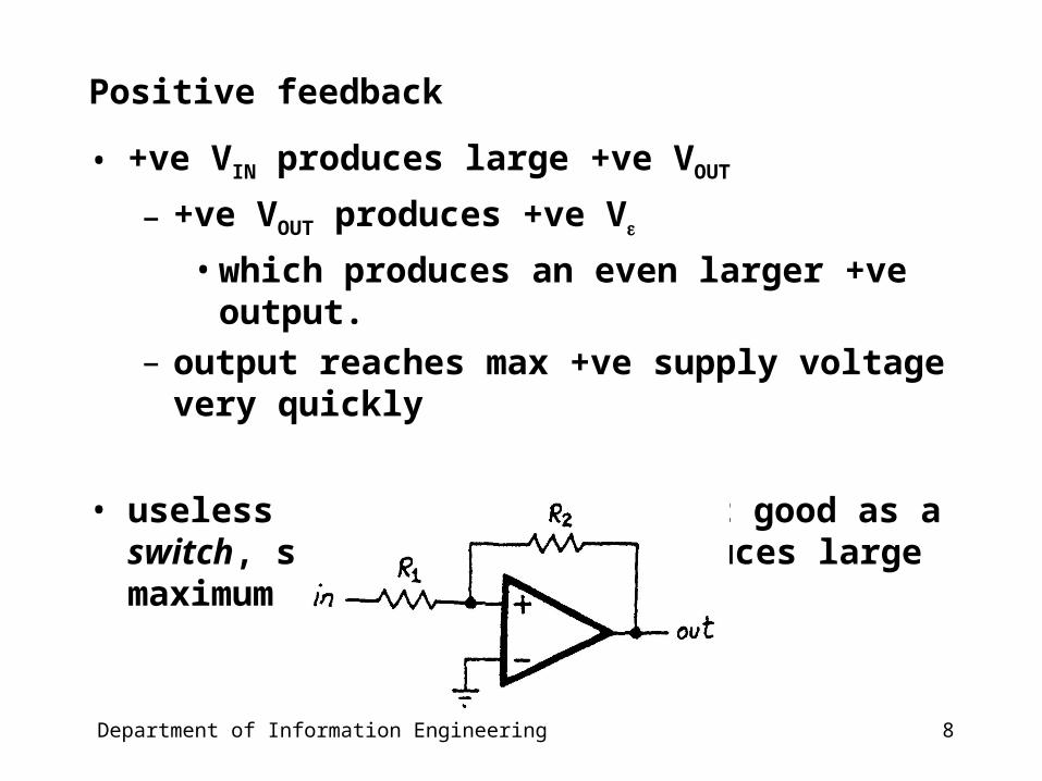
Positive feedback
• +ve VIN produces large +ve VOUT
– +ve VOUT produces +ve V
• which produces an even larger +ve output.
– output reaches max +ve supply voltage very quickly
• useless as an amplifier (but good as a switch, small +ve signal produces large maximum output)

9Department of Information Engineering
Non-inverting amplifier
• RIN?
– infinite !
• V-?
– V- ~ VIN (V ~ 0)
• Current through R1?
– I=VIN / R1
• Output voltage?
–
V-
IN1
2121OUT V
RRR
)RR(IV
V

10Department of Information Engineering
Voltage follower
• Left side circuit (work)
– If output is too large, then feedback to the –ve terminal will reduce output to a equilibrium level until V ~ 0
• Right side circuit (doesn’t work)
– If output is too large, then feedback to the +ve terminal will make the output even larger until saturation

11Department of Information Engineering
Power booster
• The output current of an op amp is usually small
• If you want larger output current, add an external push-pull follower made of discrete power transistors

12Department of Information Engineering
Power booster
• Normally push-pull follower has cross-over distortion
– Not this one !
• The gain of the amplifier depends on the external feedback circuit
• The forward gain of the internal circuit can be non-linear but must be large

13Department of Information Engineering
Power of feedback
• Can put in anything in the forward loop, still get good result

14Department of Information Engineering
Funny circuits
• What is the function of this circuit?

15Department of Information Engineering
Funny circuits
• Does this circuit work?

16Department of Information Engineering
Practical circuits
• Design an inverting amplifier with a gain of -100, to be driven by a source whose output impedance is 1M– What is the value of R? How about 100R?

17Department of Information Engineering
Practical circuits
• A better solution
18Department of Information Engineering
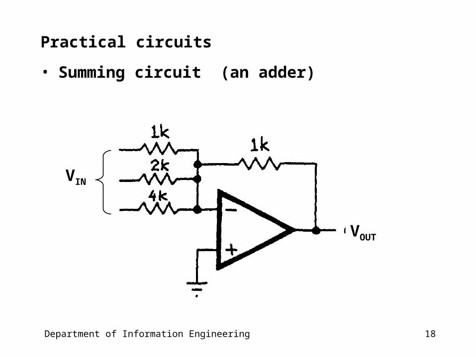
Practical circuits
• Summing circuit (an adder)
VIN
VOUT

19Department of Information Engineering
•
•
3213
32
21
1 IIII,k4
VI,
k2V
I,k1
VI
)4/V2/VV(
k1k4
V
k2V
k1V
k1IV
321
321OUT
V1
V2
V3
I
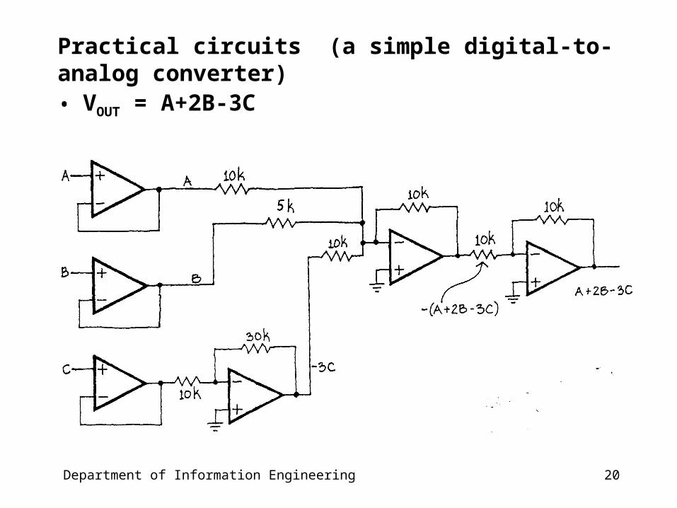
20Department of Information Engineering
Practical circuits (a simple digital-to-analog converter)
• VOUT = A+2B-3C
21Department of Information Engineering
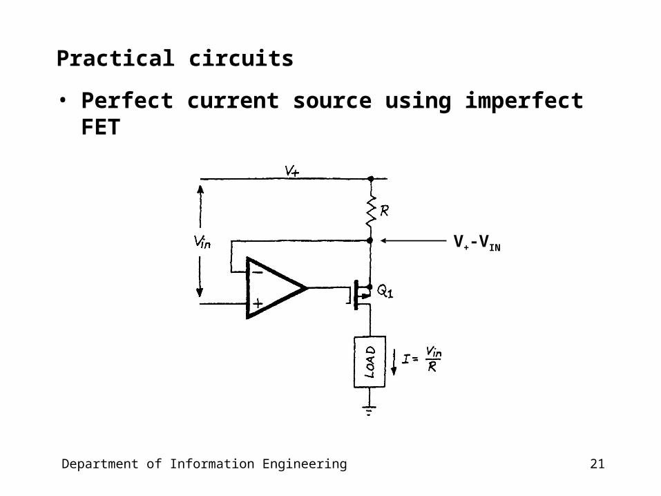
Practical circuits
• Perfect current source using imperfect FET
V+-VIN
22Department of Information Engineering
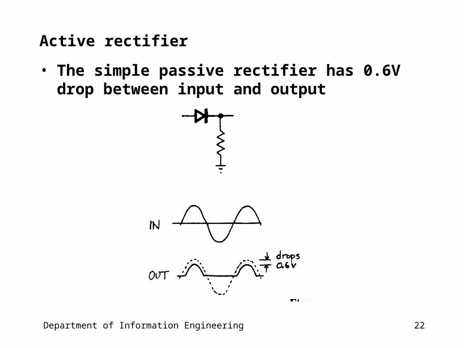
Active rectifier
• The simple passive rectifier has 0.6V drop between input and output
23Department of Information Engineering
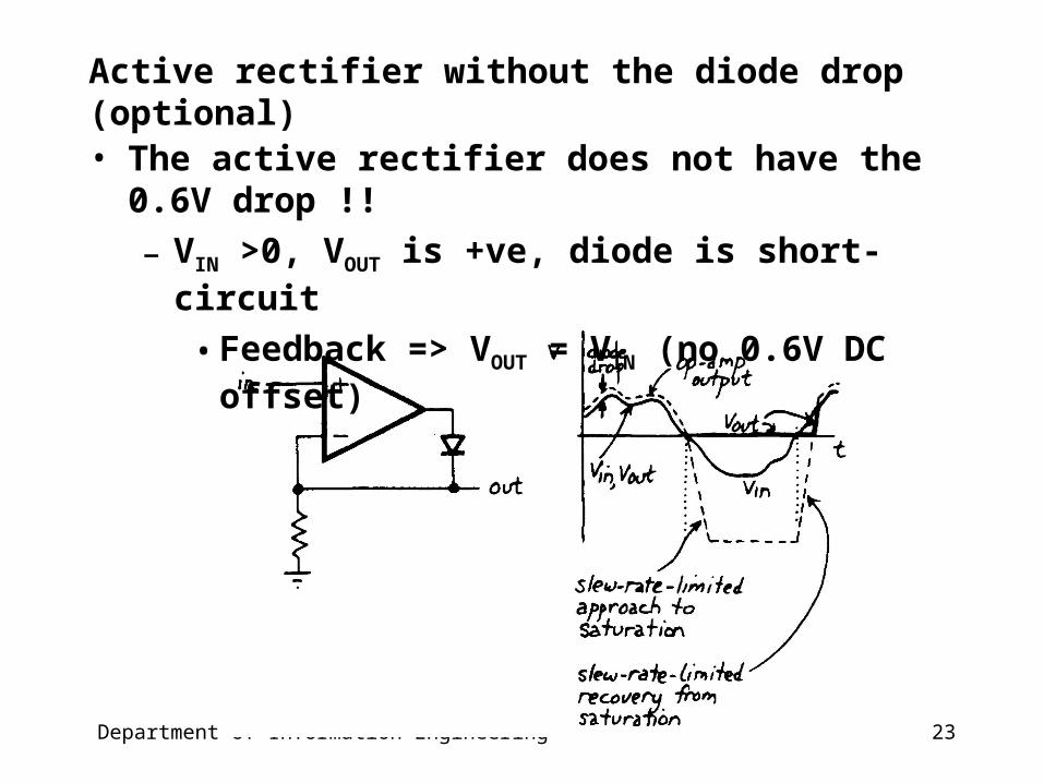
Active rectifier without the diode drop (optional)
• The active rectifier does not have the 0.6V drop !!
– VIN >0, VOUT is +ve, diode is short-circuit
• Feedback => VOUT = VIN (no 0.6V DC offset)

24Department of Information Engineering
Problem
• –ve input to V+, VOUT , diode is open circuit
• VOUT pushes to –ve extreme
• When input becomes +ve, takes a long time for the output to move from –ve to +ve (limited by the slew rate)

25Department of Information Engineering
Active rectifier (optional)
• This improved circuit prevents the rectifier from saturation

26Department of Information Engineering
Negative-impedance converter (NIC)
• An interesting two-terminals active device
– apply a +ve voltage, you see a current flowing OUT
– a negative impedance (!!)
– i.e. ZIN = - Z !!
– (leave the proof as exercise)

27Department of Information Engineering
Gyrator
• The following circuit is a gyrator
– (leave the proof as exercise)ZR
Z2
in
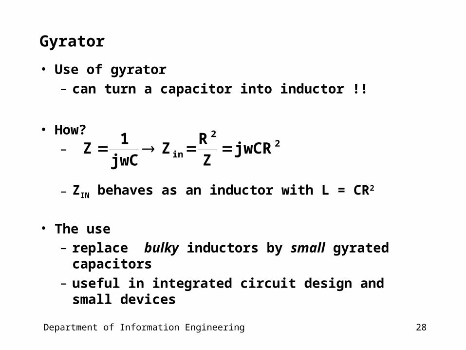
28Department of Information Engineering
Gyrator
• Use of gyrator
– can turn a capacitor into inductor !!
• How?
–
– ZIN behaves as an inductor with L = CR2
• The use– replace bulky inductors by small gyrated capacitors
– useful in integrated circuit design and small devices
22
in jwCRZ
RZ
jwC1
Z

29Department of Information Engineering
Positive feedback
• Apply feedback to the non-inverting (+ve) terminal
– small +ve input produces a larger +ve output
– output is feedback to the non-inverting input
– produces an even larger output
– quickly push the output to saturation
• Uses
– Comparators
– Oscillators

30Department of Information Engineering
Comparator – a simple switch
• Output = +15V if VIN < 0
• Output = -15V if VIN > 0
VIN -
+
VOUT
+15V
-15V

31Department of Information Engineering
• A poor comparator because
– if the input is noisy, the output makes several transitions (switching noise)

32Department of Information Engineering
311 op amp
• The output stage (emitter follower) is connected to external power supply
• User can choose the output voltage they like
33Department of Information Engineering
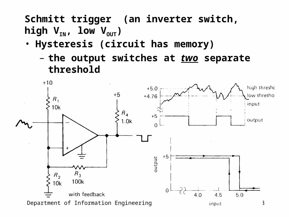
Schmitt trigger (an inverter switch, high VIN, low VOUT)
• Hysteresis (circuit has memory)
– the output switches at two separate threshold

34Department of Information Engineering
Analysis
• If VOUT = high (~5V)
– VOUT ~= 5V,
– Switching threshold V+ = 5V
• When VIN > 5V
– VOUT =0V
– Switching threshold V+=4.76V
• Now if VIN drops slightly below 5V
– VOUT won’t change state
– Eliminate noisy switching
10V 5V
10K
10K100K
1K
V+

35Department of Information Engineering
Analysis
• VIN > 5V, VOUT=0V, V+ =4.76V
• If VIN < 4.76V, VOUT=5V,
– V+ =5V (the new threshold)
10V
10K
10K100K
V+ 0V

36Department of Information Engineering
Positive feedback
• if phase shift = 180o in box ‘X’ at certain frequency, then the feedback becomes +ve (unstable) !!
• This high frequency has sustained itself even there is no input
– oscillation

37Department of Information Engineering
Nasty oscillators
• A follower driving a long cable (a common problem)
– phase shift through the op amp = 180o
– cable’s capacitance adds another 90o
– The internal capacitance at high frequency adds another 90o
• The follower oscillates !
(cable capacitance)

38Department of Information Engineering
Ways to break the oscillation
• Op amp oscillates at high frequency because of the additional phase shift introduced by its internal capacitor
• Solution
– Reduce the loop gain AB at high frequency
• At the frequency that may cause oscillation, make A ~ 0, so that the loop gain (AB) < 1
– Op am that does this is called frequency compensated op amp
• Disadvantage is that the max bandwidth is reduced

39Department of Information Engineering
• One oscillates, the other not
– 411 is frequency compensated, never oscillates
411 311
Never oscillates May oscillates
|A|
f
|A|
ffocc
40Department of Information Engineering
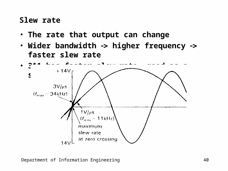
Slew rate
• The rate that output can change
• Wider bandwidth higher frequency faster slew rate
• 311 has faster slew rate, good as a switch

41Department of Information Engineering
• What is the use of these two resistors?