design example report - power · design example report ... no damage during line brown-out or...
TRANSCRIPT

Power Integrations 5245 Hellyer Avenue, San Jose, CA 95138 USA. Tel: +1 408 414 9200 Fax: +1 408 414 9201
www.power.com
Design Example Report
Title 12 W High Efficiency, High Power Factor, Isolated Flyback Power Supply Using InnoSwitchTM-CH INN2003K
Specification 90 VAC – 265 VAC Input; 30 V, 400 mA Output
Application Smart Lighting with Casambi CBM-001
Author Applications Engineering Department
Document Number DER-612
Date December 14, 2017
Revision 1.1
Summary and Features Accurate constant voltage regulation Fast transient load response High power factor Highly energy efficient Low standby power Low component count Integrated protection and reliability features
Output short-circuit Line and output OVP Line surge or line overvoltage Over temperature shutdown with hysteretic automatic power recovery
No damage during line brown-out or brown-in conditions Meets IEC 2.5 kV ring wave, 2 kV differential surge Meets EN55015 conducted EMI

DER-612 12 W High Efficiency Isolated Flyback using InnoSwitch-CH 14-Dec-17
Page 2 of 78
Power Integrations, Inc. Tel: +1 408 414 9200 Fax: +1 408 414 9201 www.power.com
PATENT INFORMATION The products and applications illustrated herein (including transformer construction and circuits external to the products) may be covered by one or more U.S. and foreign patents, or potentially by pending U.S. and foreign patent applications assigned to Power Integrations. A complete list of Power Integrations' patents may be found at www.powerint.com. Power Integrations grants its customers a license under certain patent rights as set forth at <http://www.powerint.com/ip.htm>. `

14-Dec-17 DER-612 12 W High Efficiency Isolated Flyback using InnoSwitch-CH
Page 3 of 78
Power Integrations Tel: +1 408 414 9200 Fax: +1 408 414 9201
www.power.com
Table of Contents 1 Introduction ....................................................................................................... 6 2 Power Supply Specification .................................................................................. 8 3 Schematic .......................................................................................................... 9 4 Circuit Description ............................................................................................ 10
4.1 Input EMI Filter and Rectifier ...................................................................... 10 4.2 Valley-Fill PFC Circuit ................................................................................. 10 4.3 InnoSwitch-CH Primary Side Control ............................................................ 11 4.4 InnoSwitch-CH Secondary Side Control ........................................................ 12
5 PCB Layout ...................................................................................................... 15 6 Bill of Materials ................................................................................................ 16
6.1 Miscellaneous Parts .................................................................................... 17 7 Flyback Transformer Specification (T1) .............................................................. 18
7.1 Electrical Diagram ...................................................................................... 18 7.2 Electrical Specifications .............................................................................. 18 7.3 Material List .............................................................................................. 18 7.4 Transformer Construction ........................................................................... 19 7.5 Winding Illustrations .................................................................................. 20
8 Transformer Spreadsheet .................................................................................. 26 9 Performance Data ............................................................................................ 29
9.1 System Efficiency ....................................................................................... 29 9.2 Output Voltage Regulation .......................................................................... 30 9.3 Power Factor ............................................................................................. 31 9.4 %ATHD .................................................................................................... 32 9.5 No-Load Input Power ................................................................................. 33 9.6 No-Load Output Voltage ............................................................................. 34
10 Test Data ..................................................................................................... 35 10.1 Test Data at Full Load ................................................................................ 35 10.2 Test Data at No-Load ................................................................................. 35
11 Load Regulation Performance ........................................................................ 36 11.1 Output Voltage Load Regulation .................................................................. 36 11.2 Efficiency vs. Load ..................................................................................... 37 11.3 Average Efficiency ..................................................................................... 38
11.3.1 Average Efficiency Measurement .......................................................... 38 11.4 Power Factor vs. Load ................................................................................ 39 11.5 %ATHD vs. Load ....................................................................................... 40
12 Thermal Performance .................................................................................... 41 12.1 Thermal Scan at 25 ºC Ambient .................................................................. 41
12.1.1 Thermal Scan at 90 VAC Full Load ........................................................ 42 12.1.2 Thermal Scan at 115 VAC Full Load ...................................................... 43 12.1.3 Thermal Scan at 230 VAC Full Load ...................................................... 44 12.1.4 Thermal Scan at 265 VAC Full Load ...................................................... 45
12.2 Thermal Test at 75 0C Ambient ................................................................... 46

DER-612 12 W High Efficiency Isolated Flyback using InnoSwitch-CH 14-Dec-17
Page 4 of 78
Power Integrations, Inc. Tel: +1 408 414 9200 Fax: +1 408 414 9201 www.power.com
12.3 Thermal Test Data at 75 ºC Ambient ........................................................... 47 12.4 Electrical Test Data at 75 ºC Ambient .......................................................... 47
13 Waveforms ................................................................................................... 48 13.1 Input Voltage and Input Current at Full Load ............................................... 48 13.2 Start-up Profile at Full Load ........................................................................ 49 13.3 Output Voltage Fall .................................................................................... 50 13.4 Power Cycling ........................................................................................... 51 13.5 Load Transient Response 3 Hz .................................................................... 52 13.6 Load Transient Response 100 Hz ................................................................ 53 13.7 InnoSwitch-CH Drain Voltage and Current Waveforms .................................. 54 13.8 InnoSwitch-CH Drain Voltage and Current at Full Start-up ............................. 56 13.9 InnoSwitch-CH Drain Voltage and Current During Output Short-Circuit ........... 57 13.10 Input Power at Short-Circuit .................................................................... 57 13.11 Output Ripple Voltage ............................................................................. 58
14 Conducted EMI ............................................................................................. 59 14.1 Test Set-up ............................................................................................... 59 14.2 Equipment and Load Used .......................................................................... 59 14.3 EMI Test Result ......................................................................................... 60
15 Line Surge .................................................................................................... 62 15.1 Differential Surge Test Results .................................................................... 62 15.2 Ring Wave Test Results .............................................................................. 63 15.3 Differential Surge (1 KV) ............................................................................ 64 15.4 Ring Wave Test (2.5 kV) ............................................................................ 64
16 Brown-in/Brown-out Test .............................................................................. 65 17 Appendix ...................................................................................................... 66
17.1 Application Example ................................................................................... 66 17.1.1 Smart RGBW Downlight with BLE Control .............................................. 66 17.1.2 BLE Interface Circuitry ......................................................................... 66
17.2 RGBW LED Load Engine ............................................................................. 70 17.3 How to Configure the Casambi CBM-001 Module .......................................... 73 17.4 Complete Assembly of the Application Example ............................................ 74 17.5 Bill of Materials – BLE Interface Circuitry ..................................................... 75 17.6 Bill of Materials – RGBW LED Engine ........................................................... 76
18 Revision History ............................................................................................ 77

14-Dec-17 DER-612 12 W High Efficiency Isolated Flyback using InnoSwitch-CH
Page 5 of 78
Power Integrations Tel: +1 408 414 9200 Fax: +1 408 414 9201
www.power.com
Important Note: Although this board is designed to satisfy safety isolation requirements, the engineering prototype has not been agency approved. Therefore, all testing should be performed using an isolation transformer to provide the AC input to the prototype board.

DER-612 12 W High Efficiency Isolated Flyback using InnoSwitch-CH 14-Dec-17
Page 6 of 78
Power Integrations, Inc. Tel: +1 408 414 9200 Fax: +1 408 414 9201 www.power.com
1 Introduction This engineering report describes a constant voltage (CV) output 12 W isolated flyback power supply with a valley-fill passive power factor correction circuit for smart lighting applications. The power supply is designed to provide a 30 V constant voltage output across 0 mA to 400 mA output current load and throughout the input voltage from 90 VAC to 265 VAC. The power supply IC controller device, InnoSwitch-CH combines primary, secondary and feedback circuits in a single surface-mounted off-line flyback switcher IC. It incorporates the primary FET, the primary side controller and a secondary-side synchronous rectification controller. The device also includes an innovative new technology, FluxLink™, which safely bridges the isolation barrier and eliminates the need for an optocoupler. The added valley-fill passive power factor correction circuit is a simple and low cost solution to meet power factor requirements for lighting applications. DER-612 using InnoSwitch-CH offers a highly efficient constant voltage supply with a fast transient load response. The design achieves high power factor (0.9) at low line. The key design goals were high efficiency, optimized power factor and low components count. The document contains the power supply specification, schematic, bill of materials, transformer documentation, printed circuit layout, design spreadsheet, sample actual application circuit in Appendix section, and performance data.
Figure 1 – Populated Circuit Board.

14-Dec-17 DER-612 12 W High Efficiency Isolated Flyback using InnoSwitch-CH
Page 7 of 78
Power Integrations Tel: +1 408 414 9200 Fax: +1 408 414 9201
www.power.com
Figure 2 – Populated Circuit Board, Top View.
Figure 3 – Populated Circuit Board, Bottom View.

DER-612 12 W High Efficiency Isolated Flyback using InnoSwitch-CH 14-Dec-17
Page 8 of 78
Power Integrations, Inc. Tel: +1 408 414 9200 Fax: +1 408 414 9201 www.power.com
2 Power Supply Specification The table below represents the minimum acceptable performance of the design. Actual performance is listed in the results section.
Description Symbol Min Typ Max Units Comment Input 115/60
230/50
Voltage VIN 90 265 Vac/Hz 2 Wire – no P.E.
Frequency fLINE
Output
Output Voltage VOUT 26.5 30 V
Output Current (Full Load) IOUT 400 mA
Output Power
Continuous Output Power POUT 12 W
Full Efficiency 84 % At 115 V / 60 Hz.
89 At 230 V / 50 Hz.
Average Efficiency 83 % DOE Level VI.
Environmental
Conducted EMI CISPR 15B / EN55015B
Safety Isolated
Ring Wave (100 kHz) Differential Mode Surge (L1-L2)
2.5
1.0
kV
kV
Power Factor 0.9 Measured at 115 V / 60 Hz.
Ambient Temperature TAMB 70 oC Free Air Convection, Sea Level.

14-Dec-17 DER-612 12 W High Efficiency Isolated Flyback using InnoSwitch-CH
Page 9 of 78
Power Integrations Tel: +1 408 414 9200 Fax: +1 408 414 9201
www.power.com
3 Schematic
Figure 4 – Schematic.
DER-612 12 W High Efficiency Isolated Flyback using InnoSwitch-CH 14-Dec-17
Page 10 of 78
Power Integrations, Inc. Tel: +1 408 414 9200 Fax: +1 408 414 9201 www.power.com
4 Circuit Description InnoSwitch-CH (INN2003K) incorporates the primary FET, the primary side controller and a secondary-side synchronous rectification controller. This IC also includes an innovative new technology, FluxLink™, which safely bridges the isolation barrier and eliminates the need for an optocoupler. InnoSwitch-CH is configured to drive a 12 W flyback power supply with added valley-fill passive PFC circuit providing a high power factor 30 V constant voltage supply throughout the input range of 90 VAV to 265 VAC.
4.1 Input EMI Filter and Rectifier The input fuse F1 provides safety protection from component failures. Varistor RV1 acts as a voltage clamp that limits the voltage spike on the primary during line transient voltage surge events. A 275 V rated part was selected, being slightly above the maximum specified operating input voltage (265 V). The AC input voltage is full wave rectified by BR1 to achieve good power factor and low THD. The bulk capacitor C2 and C3 provides input line ripple voltage filtering for a stable flyback DC supply voltage. Capacitor C1, L1, L2, C4 and C15 provide EMI filtering to suppress differential mode noise caused by the PFC and flyback switching action. Common mode noise is suppressed by Y-capacitor C13. These together with the InnoSwitch-CH frequency jitter and electronically quiet source pins ensure compliance with EN55015B.
4.2 Valley-Fill PFC Circuit Off-line flyback power supplies without PFC usually consist of an input bridge rectifier followed by a storage bulk capacitor. The input line current is drawn in high amplitude narrow pulses near the peaks of the voltage waveform introducing high input RMS current and high harmonic distortion. The valley-fill PFC is a simple low cost solution to improve power factor.

14-Dec-17 DER-612 12 W High Efficiency Isolated Flyback using InnoSwitch-CH
Page 11 of 78
Power Integrations Tel: +1 408 414 9200 Fax: +1 408 414 9201
www.power.com
Figure 5 – Valley-Fill PFC.
Capacitor C2 and C3 are charged through diode D3 while the input rectified AC voltage approaches VPEAK/2 increasing the input current conduction angle. Resistor R7 reduces peak current that will increase RMS current and harmonic distortion. When the input rectified AC voltage is greater than VPEAK/2 the flyback converter switches with its supply current drawn directly from the input DC bus supply. Capacitor C4 and C15 filter the switching voltage spikes that appear on the DC bus supply. Diode D1 and D2 block current from charging C2 and C3 when the input rectified voltage is less than half of the VPEAK. Capacitor C2 and C3 supply current through D1 and D2 while the input rectified voltage is below VPEAK/2. At this time C2 and C3 are basically in parallel.
4.3 InnoSwitch-CH Primary Side Control The isolated flyback power supply is controlled by InnoSwitch-CH (INN2003K). One side of the transformer (T1) primary is connected to the positive DC bus terminal while the other side is connected to the drain pin of the InnoSwitch-CH (U1) internal power MOSFET. A low cost RCD clamp formed by D4, R8, C5 and R1 limits the peak drain voltage spike due to the effects of transformer leakage inductance. During the initial power-up, the internal high-voltage current source charges the (BPP) pin capacitor (C7) initializing the switching via primary side control. The secondary side assumes the control after a handshake initiating a normal switching operation. During normal operation the primary side block is powered by the auxiliary winding of the transformer. The output of this is configured as a flyback winding, rectified and filtered by D5 and C6 and fed to the BPP pin via a current limiting resistor R2.

DER-612 12 W High Efficiency Isolated Flyback using InnoSwitch-CH 14-Dec-17
Page 12 of 78
Power Integrations, Inc. Tel: +1 408 414 9200 Fax: +1 408 414 9201 www.power.com
Output regulation is achieved using On/Off control, the number of enabled switching cycles are adjusted based on the output load. At high load most switching cycles are enabled, and at light load or no-load most cycled are disabled or skipped. Once a cycle is enabled, the power MOSFET remains on until the primary current ramps to the device current limit for the specific operating state. There are four operating states (current limits) arranged such that the frequency content of the primary current switching pattern remains out of the audible range until light load where the transformer flux density and therefore audible noise generation is at a very low level.
4.4 InnoSwitch-CH Secondary Side Control The transformer secondary is rectified by a low VF Schottky diode D7 and filtered by the output capacitor C10. R-C snubber R4 and C9 reduces voltage stress on D7 and radiated EMI. For high output voltage designs a low voltage secondary bias is needed to ensure that the VO pin rating is not exceeded. The FWD pin is connected to the secondary bias winding and the VO pin to the secondary bias supply. The secondary bias winding voltage is rectified by D6 and C8 and is set at 10 V. The secondary side of the IC is self-powered from either the secondary bias winding forward voltage or 10 V bias supply. During the on-time of the primary side MOSFET the forward voltage that appears across the secondary bias winding is used to charge the BPS capacitor (C11) via FWD pin resistor (R3) and an internal regulator. During CV operation, the 10 V secondary bias powers the secondary side control. The unit enters auto-restart when the VO pin voltage is lower than 3 V. The output voltage is sensed via resistor divider R5 and R6 during CV operation and is compared to a reference voltage of 1.265 V on the FB pin when at the regulated output voltage. Filter capacitor C12 is added across R6 to eliminate unwanted noise that might trigger the OVP or increase ripple voltage. Output current is sensed internally between the IS and GND pins with a threshold of 35 mV to minimize losses. Once the internal current sense threshold is exceeded, the device adjusts the number of enabled switching cycles to maintain a fixed output current. Diode D8 protects the IS pin from high inrush current during output short-circuit. It is necessary to use C8 at 680 F to be able to supply the wireless module for a certain period of time after the mains input is turned OFF. This enables the wireless module to handle the Power-OFF detection functionality. Zener diode VR1 and a resistor R12 are to ensure the auxiliary power supply will not drop significantly when the LED output is turned OFF via the wireless module since the feedback close-loop is tied to the main output. The value of VR1 must be carefully chosen so as not to conduct when the output

14-Dec-17 DER-612 12 W High Efficiency Isolated Flyback using InnoSwitch-CH
Page 13 of 78
Power Integrations Tel: +1 408 414 9200 Fax: +1 408 414 9201
www.power.com
is loaded; that is, VZ = (VOUT – V_AUX_NL) and the difference between V_AUX_FL and V_AUX_NL is greater than the tolerance of the Zener diode. Figure 6 illustrates the voltage levels of the secondary main output and auxiliary output in consideration. VOUT is the main output voltage while V_AUX_FL and V_AUX_NL are the auxiliary output when the main output is at full load and at no-load conditions, respectively. Take note that the secondary auxiliary supply still has to power the BLE module and the gate drivers even when the main output is at no-load condition (which happens when the LED load is turned OFF via the Casambi App). V_AUX_NL should be set at a level enough to supply the BLE module and should not cause the InnoSwitch-CH IC to reset due to low BPS pin voltage; V_AUX_NL ≥ 4.5 V should be good enough for this application.

DER-612 12 W High Efficiency Isolated Flyback using InnoSwitch-CH 14-Dec-17
Page 14 of 78
Power Integrations, Inc. Tel: +1 408 414 9200 Fax: +1 408 414 9201 www.power.com
VOUT
V_AUX_FL
V_AUX_NL
GND
Where: Vout – main output voltage
V_AUX_FL – secondary auxiliary voltage when the main output is at Full Load
V_AUX_NL – desired secondary auxiliary voltage when the main output is at No Load
Figure 6 – Secondary Output Voltage Levels.

14-Dec-17 DER-612 12 W High Efficiency Isolated Flyback using InnoSwitch-CH
Page 15 of 78
Power Integrations Tel: +1 408 414 9200 Fax: +1 408 414 9201
www.power.com
5 PCB Layout
Figure 7a – Top Side.
Figure 7b – Bottom Side.

DER-612 12 W High Efficiency Isolated Flyback using InnoSwitch-CH 14-Dec-17
Page 16 of 78
Power Integrations, Inc. Tel: +1 408 414 9200 Fax: +1 408 414 9201 www.power.com
6 Bill of Materials Item Qty Ref
Des Description Mfg Part Number Mfg
1 1 BR1 1000 V, 0.8 A, Bridge Rectifier, SMD, MBS-1, 4-SOIC B10S-G Comchip 2 1 C1 100 nF, 450 V, Film MEXXD31004JJ1 Duratech 3 1 C2 27 F, 200 V, Electrolytic, (10 x 16), EKXJ201ELL270MJ16S Nippon Chemi-Con 4 1 C3 27 F, 200 V, Electrolytic, (10 x 16), EKXJ201ELL270MJ16S Nippon Chemi-Con 5 1 C4 100 nF, 450 V, Film MEXXD31004JJ1 Duratech 6 1 C5 1 nF, 250 V, Ceramic, X7R, 0805 GRM21AR72E102KW01D Murata 7 1 C6 22 F, 16 V, Ceramic, X5R, 0805 C2012X5R1C226K TDK 8 1 C7 1 F,50 V, Ceramic, X7R, 0805 C2012X7R1H105M085AC TDK 9 1 C8 680 F, 16 V, Electrolytic, (10 x 12.5) KMG16WV680UF10X12.5 Sam Young 10 1 C9 100 pF, 500 V, Ceramic, NPO, 0805 501R15N101KV4T Johanson Dielectrics 11 1 C10 470 F, 35 V, Electrolytic, Low ESR, 23 m, (10 x 20) UHD35470MPD Nichicon 12 1 C11 2.2 F, 25 V, Ceramic, X7R, 0805 C2012X7R1E225M TDK 13 1 C12 100 pF 100V 10 % X7R 0805 08051C101JAT2A AVX 14 1 C13 2.2 nF, Ceramic, Y1 CD90ZU2GA222MYNKA TDK 15 1 C15 100 nF, 450 V, Film MEXXD31004JJ1 Duratech 16 1 D1 600 V, 1 A, Standard Recovery, SMA S1J-13-F Diodes, Inc. 17 1 D2 600 V, 1 A, Standard Recovery, SMA S1J-13-F Diodes, Inc. 18 1 D3 600 V, 1 A, Standard Recovery, SMA S1J-13-F Diodes, Inc. 19 1 D4 600 V, 1 A, Rectifier, Glass Passivated, POWERDI123 DFLR1600-7 Diodes, Inc. 20 1 D5 200 V, 1 A, Rectifier, Glass Passivated, POWERDI123 DFLR1200-7 Diodes, Inc. 21 1 D6 200 V, 1 A, Rectifier, Glass Passivated, POWERDI123 DFLR1200-7 Diodes, Inc. 22 1 D7 200 V, 3 A, DIODE SCHOTTKY 1 A 200 V, SMB SK3200B-LTP Micro Commercial 23 1 D8 30 V, 1.5 A, Schottky, Low Vf, DO-214AC SL13-E3/61T Vishay 24 1 F1 2 A, 250V, Slow, Long Time Lag, RST RST 2 Belfuse
25 1 J1 CONN, Male, Vertical, 5 Positions, Header, 0.079" (2.00 mm), TH, Tin 0894000510 Molex
26 1 L1 4.7 mH, 240 mA, 9 x 12.2 mm H RLB9012-472KL PM-R30472
Bourns Premier Magnetics
27 1 L2 4.7 mH, 240 mA, 9 x 12.2 mm H RLB9012-472KL PM-R30472
Bourns Premier Magnetics
28 1 R1 RES, 510 k, 5%, 1/8 W, Thick Film, 0805 ERJ-6GEYJ514V Panasonic 29 1 R2 RES, 6.8 k, 5%, 1/8 W, Thick Film, 0805 ERJ-6GEYJ682V Panasonic 30 1 R3 RES, 47.0 , 1%, 1/8 W, Thick Film, 0805 ERJ-6ENF47R0V Panasonic 31 1 R4 RES, 20 , 5%, 1/8 W, Thick Film, 0805 ERJ-6GEYJ200V Panasonic 32 1 R5 RES, 100 k, 1%, 1/8 W, Thick Film, 0805 ERJ-6ENF1003V Panasonic 33 1 R6 RES, 4.99 k, 1%, 1/8 W, Thick Film, 0805 ERJ-6ENF4991V Panasonic
34 1 R7 RES, 68 , 5%, 3 W, Wirewound, Axial, Flame Retardant Coating, Fusible AC03000006809JACCS Vishay
35 1 R8 RES, 30 , 5%, 1/4 W, Thick Film, 1206 ERJ-8GEYJ300V Panasonic 36 1 R9 RES, 7.5 k, 5%, 1/8 W, Thick Film, 0805 ERJ-6GEYJ752V Panasonic 37 1 R10 RES, 7.5 k, 5%, 1/8 W, Thick Film, 0805 ERJ-6GEYJ752V Panasonic 38 1 R12 RES, 825 , 1%, 1/8 W, Thick Film, 0805 ERJ-6ENF8250V Panasonic 39 1 RV1 275 VAC, 23 J, 7 mm, RADIAL V275LA4P Littlefuse
40 1 T1 Bobbin, RM6_S/I, Vertical, 8 pins w 2 pin clip. Transformer
CPV-RM6S/I-1S-8PD POL-INN026
Ferroxcube Premier Magnetics
41 1 U1 InnoSwitch-CH, Off-Line CV/CC Flyback Switcher, ReSOP-16B INN2003K Power Integrations
42 1 VR1 19 V, 5%, 500 mW, DO-35 1N5249B-T Diodes, Inc.
14-Dec-17 DER-612 12 W High Efficiency Isolated Flyback using InnoSwitch-CH
Page 17 of 78
Power Integrations Tel: +1 408 414 9200 Fax: +1 408 414 9201
www.power.com
6.1 Miscellaneous Parts Item Qty Ref Description Mfg Part
Number Mfg
1 4 FL1, FL2, FL3, FL4 Flying Lead, Hole size 50mils N/A N/A
2 1 TP1 Test Point, WHT, THRU-HOLE MOUNT 5012 Keystone 3 1 TP2 Test Point, BLK, THRU-HOLE MOUNT 5011 Keystone 4 1 TP3 Test Point, BLK, Miniature THRU-HOLE MOUNT 5001 Keystone 5 1 TP4 Test Point, RED, Miniature THRU-HOLE MOUNT 5000 Keystone

DER-612 12 W High Efficiency Isolated Flyback using InnoSwitch-CH 14-Dec-17
Page 18 of 78
Power Integrations, Inc. Tel: +1 408 414 9200 Fax: +1 408 414 9201 www.power.com
7 Flyback Transformer Specification (T1)
7.1 Electrical Diagram
Figure 8 – Transformer Electrical Diagram. Figure 9 – Transformer Mechanical Diagram.
7.2 Electrical Specifications Parameter Condition Spec.
Nominal Primary Inductance
Measured at 1 VPK-PK, 100 kHz switching frequency, between pin 3 and pin 4 with all other windings open. 630 H
Tolerance Tolerance of Primary Inductance. ±5%
7.3 Material List Item Description [1] Core: RM6 PC95. [2] Bobbin, RM6_S/I, Vertical, 8 pins w 2 pin clip: 25-00915-00. [3] Magnet Wire: #33 AWG. [4] TIW: #25 AWG. [5] TIW: #32 AWG. [6] Polyester Tape: 6.5 mm. [7] Mounting Clip: RM6 S/I.

14-Dec-17 DER-612 12 W High Efficiency Isolated Flyback using InnoSwitch-CH
Page 19 of 78
Power Integrations Tel: +1 408 414 9200 Fax: +1 408 414 9201
www.power.com
7.4 Transformer Construction
Winding Directions Bobbin is oriented on winder jig such that terminal pin 1-4 is in the left side. The winding direction is clockwise.
Winding 1
Use magnetic wire Item [3]. Prepare an enough length of magnetic wire for primary winding (56 turns). Start the winding 1 at pin 3 and wind 28 turns evenly. Set aside the remaining length of magnetic wire on the left side and reserve it for Winding 3. Do not cut the wire and temporally fix it on terminal pin 4 so it will not loosen up during Winding 2.
Insulation Apply 1 layer of polyester tape, Item [6] for insulation
Winding 2
Use triple insulated wire Item [4]. The terminals for Winding 2 are fly wires marked as (FL1) and (FL2). Start the Winding 2 at FL1 and wind 17 turns evenly in 2 layers. Finish the winding on FL2. Temporally use the bobbin terminals to fix the FL1 and FL2 so it will not loosen up.
Insulation Apply 1 layer of polyester tape, Item [6] for insulation.
Winding 3 Use the remaining magnetic wires from Winding 1 reserved for winding 3 on the left side. Start the winding on the left side as shown in the figure and 28 turns evenly. Finish the winding on pin 4.
Insulation Apply 1 layer of polyester tape, Item [6] for insulation
Winding 4 Use magnetic wire Item [3]. Start at pin 1 and wind 6 turns tightly. Finish the winding on pin 2.
Winding 5
Use triple insulated wire item [5]. The terminals for Winding 5 are fly wires marked as (FL3) and (FL4). Start Winding 5 at FL3 and wind 6 turns evenly beside Winding 4. Finish the winding on FL4. Temporally use the bobbin terminals to fix fly wire terminals (FL3) and (FL4) so it will not loosen up.
Insulation Apply 1 layer of polyester tape, Item [6] for insulation
TIW wire twisting Twist wire FL1/FL2 and FL3/FL4 to minimize the loop that may increase the EMI.
Core Grinding Grind the center leg of the ferrite core to meet the nominal inductance specification of 620 H.
Core Fixing Assemble the ferrite cores on the bobbin. Apply the mounting clips to fix the cores.
Pins Cut pin 6 -8. Cut Pin 5 horizontal Pin. Do not cut the mounting clip terminal pin located on the left side near the C13.
Finished Dip the finished transformer into 2:1 varnish thinner solution.

DER-612 12 W High Efficiency Isolated Flyback using InnoSwitch-CH 14-Dec-17
Page 20 of 78
Power Integrations, Inc. Tel: +1 408 414 9200 Fax: +1 408 414 9201 www.power.com
7.5 Winding Illustrations Winding Directions Bobbin is oriented on winder jig such that terminal pin 1-4 is in the left side. The winding direction is clockwise. Winding 1 Use magnetic wire item 3. Prepare an enough length of magnetic wire for primary winding (56 turns). Start the winding 1 at pin 3 and wind 28 turns evenly. Set aside the remaining length of magnetic wire on the left side and reserve it for Winding 3. Do not cut the wire and temporally fix it on terminal pin 4 so it will not loosen up during Winding 2.
Insulation Apply 1 layer of polyester tape, Item [6] for insulation.
Pin 1
Pin 3
Pin 4
Pin 3
Pin 4
1 layer tape
Magnetic wires for Winding 3

14-Dec-17 DER-612 12 W High Efficiency Isolated Flyback using InnoSwitch-CH
Page 21 of 78
Power Integrations Tel: +1 408 414 9200 Fax: +1 408 414 9201
www.power.com
Winding 2 Use triple insulated wire item [4]. The terminals for Winding 2 are fly wires marked as (FL1) and (FL2). Start the Winding 2 at FL1 and wind 17 turns evenly in 2 layers. Finish the winding on FL2. Temporally use the bobbin terminals to fix the FL1 and FL2 so it will not loosen up.
Insulation Apply 1 layer of polyester tape, Item [6] for insulation
FL1
FL1
FL2

DER-612 12 W High Efficiency Isolated Flyback using InnoSwitch-CH 14-Dec-17
Page 22 of 78
Power Integrations, Inc. Tel: +1 408 414 9200 Fax: +1 408 414 9201 www.power.com
Winding 3 Use the remaining magnetic wires from Winding 1 reserved for winding 3 on the left side. Start the winding on the left side as shown in the figure and 28 turns evenly. Finished the winding on pin 4.
Insulation Apply 1 layer of polyester tape, Item [6] for insulation.
Winding 3
Pin 4
1 layer tape

14-Dec-17 DER-612 12 W High Efficiency Isolated Flyback using InnoSwitch-CH
Page 23 of 78
Power Integrations Tel: +1 408 414 9200 Fax: +1 408 414 9201
www.power.com
Winding 4 Use magnetic wire Item (3). Start at pin 1 and wind 6 turns tightly. Finish the winding on pin 2.
Pin 2
Winding 4
Pin 1

DER-612 12 W High Efficiency Isolated Flyback using InnoSwitch-CH 14-Dec-17
Page 24 of 78
Power Integrations, Inc. Tel: +1 408 414 9200 Fax: +1 408 414 9201 www.power.com
Winding 5 Use triple insulated wire Item [5]. The terminals for Winding 5 are fly wires marked as (FL3) and (FL4). Start Winding 5 at FL3 and wind 6 turns evenly beside Winding 4. Finish the winding on FL4. Temporally use the bobbin terminals to fix fly wire terminals (FL3) and (FL4) so it will not loosen up.
Insulation Apply 1 layer of polyester tape, Item [6] for insulation.
FL3
Winding 4
FL4
Winding 4
Winding 5
FL3

14-Dec-17 DER-612 12 W High Efficiency Isolated Flyback using InnoSwitch-CH
Page 25 of 78
Power Integrations Tel: +1 408 414 9200 Fax: +1 408 414 9201
www.power.com
TIW Wire Twisting Twist wire FL1/FL2 and FL3/FL4 to minimize the loop that may increase the EMI. Core Grinding Grind the center leg of the ferrite core to meet the nominal inductance specification of 620 H. Core Fixing Assemble the ferrite cores on the bobbin. Apply the mounting clips to fix the cores. Pins Cut pin 6-8. Cut pin 5 horizontal pin. Finished Dip the finished transformer into 2:1 varnish thinner solution.
Winding 2- Twist FL1 an FL2
Do not Cut Mounting Clip terminal pin.
Winding 5- Twist FL4 an FL5
Cut Clip Pin
Cut pin 6 -8
Pin 5
Cut this Pin

DER-612 12 W High Efficiency Isolated Flyback using InnoSwitch-CH 14-Dec-17
Page 26 of 78
Power Integrations, Inc. Tel: +1 408 414 9200 Fax: +1 408 414 9201 www.power.com
8 Transformer Spreadsheet ACDC_InnoSwitch-CH_031816; Rev.2.2; Copyright Power Integrations 2016
INPUT INFO OUTPUT UNIT ACDC_InnoSwitch-CH_031816_Rev2-2; InnoSwitch-CH Continuous/Discontinuous Flyback Transformer Design Spreadsheet
ENTER APPLICATION VARIABLES VACMIN 90 90 V Minimum AC Input Voltage VACMAX 265 265 V Maximum AC Input Voltage fL 60 60 Hz AC Mains Frequency
VO 30.00 30.00 V Output Voltage (continuous power at the end of the cable)
IO 0.40 0.40 A Power Supply Output Current (corresponding to peak power)
Power 12 W Continuous Output Power, including cable drop compensation
N 0.80 0.80 Efficiency Estimate at output terminals. Use 0.8 if no better data available
Z 0.50 0.50
Z Factor. Ratio of secondary side losses to the total losses in the power supply. Use 0.5 if no better data available
tC 3.00 mSeconds Bridge Rectifier Conduction Time Estimate CIN 22.00 22.00 uFarad Input capacitance ENTER InnoSwitch-CH VARIABLES InnoSwitch-CH Auto INN20x3 Recommended InnoSwitch-CH Cable drop compensation 0% 0% Select Cable Drop Compensation option
Complete Part Number INN2003K Final part number including package
Chose Configuration INC Increased
Current Limit
Enter "RED" for reduced current limit (sealed adapters), "STD" for standard current limit or "INC" for increased current limit (peak or higher power applications)
ILIMITMIN 0.682 A Minimum Current Limit ILIMITTYP 0.750 A Typical Current Limit ILIMITMAX 0.818 A Maximum Current Limit fSmin 93000 Hz Minimum Device Switching Frequency
I^2fmin 47.25 A^2kHz Worst case I2F parameter across the temperature range
VOR 100 100 V Reflected Output Voltage (VOR <= 100 V Recommended)
VDS 5.00 V InnoSwitch on-state Drain to Source Voltage
KP 1.41 Ripple to Peak Current Ratio at Vmin, assuming ILIMITMIN, and I2FMIN (KP < 6)
KP_TRANSIENT 0.68 Worst case transient Ripple to Peak Current Ratio. Ensure KP_TRANSIENT > 0.25
ENTER BIAS WINDING VARIABLES VB 10.00 V Bias Winding Voltage VDB 0.70 V Bias Winding Diode Forward Voltage Drop NB 5.65 V Bias Winding Number of Turns
PIVB 64.92 V Bias winding peak reverse voltage at VACmax and assuming VB*1.2

14-Dec-17 DER-612 12 W High Efficiency Isolated Flyback using InnoSwitch-CH
Page 27 of 78
Power Integrations Tel: +1 408 414 9200 Fax: +1 408 414 9201
www.power.com
ENTER TRANSFORMER CORE/CONSTRUCTION VARIABLES Core Type RM6 RM6 Enter Transformer Core Core PC47RM6Z-12 Enter core part number, if necessary Bobbin BRM6-716SPFR Enter bobbin part number, if necessary AE 0.366 cm^2 Core Effective Cross Sectional Area LE 2.86 cm Core Effective Path Length AL 1837 nH/T^2 Ungapped Core Effective Inductance BW 6.35 mm Bobbin Physical Winding Width
M 0.00 mm Safety Margin Width (Half the Primary to Secondary Creepage Distance)
L 3 Number of Primary Layers NS 17 Number of Secondary Turns DC INPUT VOLTAGE PARAMETERS VMIN 94 V Minimum DC Input Voltage VMAX 375 V Maximum DC Input Voltage CURRENT WAVEFORM SHAPE PARAMETERS
DMAX 0.53 Duty Ratio at full load, minimum primary inductance and minimum input voltage
IAVG 0.15 A Average Primary Current IP 0.682 A Peak Primary Current assuming ILIMITMIN IR 0.682 A Primary Ripple Current assuming ILIMITMIN, and LPMIN IRMS 0.26 A Primary RMS Current, assuming ILIMITMIN, and LPMIN TRANSFORMER PRIMARY DESIGN PARAMETERS
LP 635 uHenry Typical Primary Inductance. +/- 10% to ensure a minimum primary inductance of 571 uH
LP_TOLERANCE 10.0 10.0 % Primary inductance tolerance NP 56 Primary Winding Number of Turns ALG 202 nH/T^2 Gapped Core Effective Inductance
BM 2962 Gauss Maximum Operating Flux Density, BM<3000 is recommended
BAC 1481 Gauss AC Flux Density for Core Loss Curves (0.5 X Peak to Peak)
Ur 1142 Relative Permeability of Ungapped Core LG 0.20 mm Gap Length (Lg > 0.1 mm) BWE 19.05 mm Effective Bobbin Width OD 0.34 mm Maximum Primary Wire Diameter including insulation
INS 0.06 mm Estimated Total Insulation Thickness (= 2 * film thickness)
DIA 0.28 mm Bare conductor diameter
AWG 30 AWG Primary Wire Gauge (Rounded to next smaller standard AWG value)
CM 102 Cmils Bare conductor effective area in circular mils CMA 388 Cmils/Amp Primary Winding Current Capacity (200 < CMA < 500) TRANSFORMER SECONDARY DESIGN PARAMETERS Lumped parameters ISP 2.25 A Peak Secondary Current, assuming ILIMITMIN ISRMS 0.82 A Secondary RMS Current IRIPPLE 0.71 A Output Capacitor RMS Ripple Current CMS 163 Cmils Secondary Bare Conductor minimum circular mils

DER-612 12 W High Efficiency Isolated Flyback using InnoSwitch-CH 14-Dec-17
Page 28 of 78
Power Integrations, Inc. Tel: +1 408 414 9200 Fax: +1 408 414 9201 www.power.com
VOLTAGE STRESS PARAMETERS VDRAIN 525 V Maximum Drain Voltage Estimate
PIVS 191 V
Output Rectifier Maximum Peak Inverse Voltage, assuming the primary has a Voltage spike 40% above VMAX and VO*1.05
TRANSFORMER SECONDARY DESIGN PARAMETERS 1st output VO1 30.00 V Main Output Voltage directly after output rectifier IO1 0.40 A Output DC Current PO1 12.00 W Output Power VD1 0.10 V Output Synchronous Rectification FET Forward Voltage Drop NS1 17.00 Turns Output Winding Number of Turns ISRMS1 0.82 A Output Winding RMS Current IRIPPLE1 0.71 A Output Capacitor RMS Ripple Current
PIVS1 191 V
Output Rectifier Maximum Peak Inverse Voltage, assuming the primary has a Voltage spike 40% above VMAX and VO*1.05
Recommended MOSFET Si7456 Recommended SR FET for this output
RDSON_HOT 0.042 Ohm RDSon at 100C VRATED 100 V Rated voltage of selected SR FET CMS1 163 Cmils Output Winding Bare Conductor minimum circular mils AWGS1 27 AWG Wire Gauge (Rounded up to next larger standard AWG value) DIAS1 0.36 mm Minimum Bare Conductor Diameter ODS1 0.37 mm Maximum Outside Diameter for Triple Insulated Wire

14-Dec-17 DER-612 12 W High Efficiency Isolated Flyback using InnoSwitch-CH
Page 29 of 78
Power Integrations Tel: +1 408 414 9200 Fax: +1 408 414 9201
www.power.com
9 Performance Data All measurements were performed at room temperature.
9.1 System Efficiency Set-up: Open frame unit Load: 400 mA CC load Ambient Temperature: 25 ºC Soak time: 60 seconds per input line
Figure 10 – Efficiency vs. Line.
80
81
82
83
84
85
86
87
88
89
90
91
80 100 120 140 160 180 200 220 240 260 280
Effi
cien
cy (
%)
Input Voltage (VAC)

DER-612 12 W High Efficiency Isolated Flyback using InnoSwitch-CH 14-Dec-17
Page 30 of 78
Power Integrations, Inc. Tel: +1 408 414 9200 Fax: +1 408 414 9201 www.power.com
9.2 Output Voltage Regulation Set-up: Open frame unit Load: 400 mA CC load Ambient Temperature: 25 ºC Soak time: 60 seconds per input line
Figure 11 – Output Voltage Regulation vs. Line.
-5%
-4%
-3%
-2%
-1%
0%
1%
2%
3%
4%
5%
29.0
29.3
29.5
29.8
30.0
30.3
30.5
30.8
31.0
31.3
31.5
80 100 120 140 160 180 200 220 240 260 280
Out
put
Vol
taga
e (V
)
Input Voltage (VAC)

14-Dec-17 DER-612 12 W High Efficiency Isolated Flyback using InnoSwitch-CH
Page 31 of 78
Power Integrations Tel: +1 408 414 9200 Fax: +1 408 414 9201
www.power.com
9.3 Power Factor Set-up: Open frame unit Load: 400 mA CC load Ambient Temperature: 25 ºC Soak time: 60 seconds per input line
Figure 12 – Power Factor vs. Line.
0.75
0.77
0.79
0.81
0.83
0.85
0.87
0.89
0.91
0.93
0.95
80 100 120 140 160 180 200 220 240 260 280
Pow
er F
acto
r
Input Voltage (VAC)
DER-612 12 W High Efficiency Isolated Flyback using InnoSwitch-CH 14-Dec-17
Page 32 of 78
Power Integrations, Inc. Tel: +1 408 414 9200 Fax: +1 408 414 9201 www.power.com
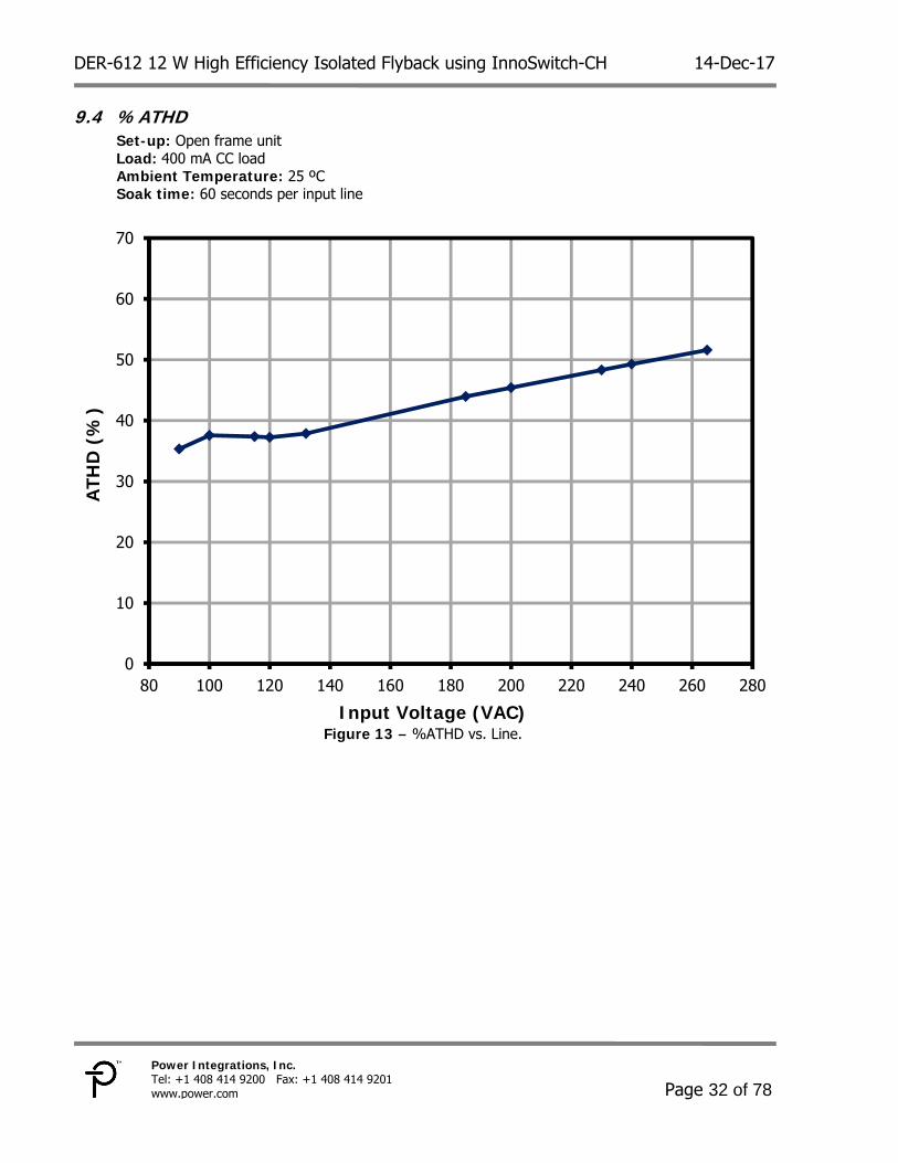
9.4 %ATHD Set-up: Open frame unit Load: 400 mA CC load Ambient Temperature: 25 ºC Soak time: 60 seconds per input line
Figure 13 – %ATHD vs. Line.
0
10
20
30
40
50
60
70
80 100 120 140 160 180 200 220 240 260 280
ATH
D (
%)
Input Voltage (VAC)

14-Dec-17 DER-612 12 W High Efficiency Isolated Flyback using InnoSwitch-CH
Page 33 of 78
Power Integrations Tel: +1 408 414 9200 Fax: +1 408 414 9201
www.power.com
9.5 No-Load Input Power Set-up: Open frame unit Load: No-load Ambient Temperature: 25 ºC Soak time: 60 seconds per line
Figure 14 – No Load Input Power vs. Line.
0
5
10
15
20
25
30
35
40
45
50
80 100 120 140 160 180 200 220 240 260 280
No-
Load
Inp
ut P
ower
(m
W)
Input Voltage (VAC)

DER-612 12 W High Efficiency Isolated Flyback using InnoSwitch-CH 14-Dec-17
Page 34 of 78
Power Integrations, Inc. Tel: +1 408 414 9200 Fax: +1 408 414 9201 www.power.com
9.6 No-Load Output Voltage
Figure 15 – No Load Voltage vs. Line.
0
5
10
15
20
25
30
35
40
45
50
55
80 100 120 140 160 180 200 220 240 260 280
No-
Load
Ou
tput
Vol
tage
(V
)
Input Voltage (VAC)

14-Dec-17 DER-612 12 W High Efficiency Isolated Flyback using InnoSwitch-CH
Page 35 of 78
Power Integrations Tel: +1 408 414 9200 Fax: +1 408 414 9201
www.power.com
10 Test Data
10.1 Test Data at Full Load
Input Input Measurement LED Load Measurement Efficiency
(%) VAC (VRMS)
Freq (Hz)
VIN (VRMS)
IIN (mARMS)
PIN (W) PF %ATHD VOUT
(VDC) IOUT
(mADC) POUT (W)
90 60 89.97 0.18 14.94 0.910 35.34 30.35 0.40 12.12 81.15 100 60 99.93 0.16 14.83 0.905 37.57 30.48 0.40 12.17 82.10 115 60 114.95 0.14 14.46 0.903 37.36 30.50 0.40 12.18 84.25 120 60 119.92 0.13 14.36 0.901 37.25 30.51 0.40 12.19 84.89 132 60 131.93 0.12 14.16 0.898 37.87 30.51 0.40 12.19 86.04 185 50 184.93 0.08 13.77 0.877 43.95 30.52 0.40 12.19 88.56 200 50 199.94 0.08 13.71 0.866 45.41 30.53 0.40 12.19 88.92 230 50 229.95 0.07 13.63 0.843 48.31 30.54 0.40 12.19 89.46 240 50 239.99 0.07 13.62 0.835 49.28 30.54 0.40 12.20 89.56 265 50 264.97 0.06 13.61 0.815 51.59 30.55 0.40 12.20 89.64
10.2 Test Data at No-Load
Input Input Measurement VOUT (VDC) VAC
(VRMS) Freq (Hz)
VIN (VRMS)
IIN (mARMS)
PIN (W)
90 60 90.01 1.88 28.90 30.62 100 60 99.95 1.80 29.50 30.62 115 60 114.97 1.62 29.50 30.63 120 60 119.94 1.54 29.10 30.63 132 60 131.95 1.41 27.70 30.63 185 50 184.93 1.05 27.50 30.63 200 50 199.94 1.05 27.70 30.63 230 50 229.96 0.94 27.90 30.63 240 50 240.00 0.96 29.00 30.62 265 50 264.97 0.91 30.00 30.63

DER-612 12 W High Efficiency Isolated Flyback using InnoSwitch-CH 14-Dec-17
Page 36 of 78
Power Integrations, Inc. Tel: +1 408 414 9200 Fax: +1 408 414 9201 www.power.com
11 Load Regulation Performance Set-up: Open frame unit Ambient Temperature: 25 ºC Soak time: 30 seconds per loading point
11.1 Output Voltage Load Regulation
Figure 16 – Output Voltage vs. Load.
-5%
-4%
-3%
-2%
-1%
0%
1%
2%
3%
4%
5%
29.0
29.3
29.5
29.8
30.0
30.3
30.5
30.8
31.0
31.3
31.5
31.8
32.0
0 10 20 30 40 50 60 70 80 90 100
Out
put
Vol
tage
(V
)
% Load
90 V 60 Hz115 V 60 Hz230 V 50 Hz265 V 50 Hz

14-Dec-17 DER-612 12 W High Efficiency Isolated Flyback using InnoSwitch-CH
Page 37 of 78
Power Integrations Tel: +1 408 414 9200 Fax: +1 408 414 9201
www.power.com
11.2 Efficiency vs. Load
Figure 17 – Efficiency vs Load.
76
78
80
82
84
86
88
90
92
20 30 40 50 60 70 80 90 100
Effi
cien
cy (
%)
% Load
90 V 60 Hz
115 V 60 Hz
230 V 50 Hz
265 V 50 Hz

DER-612 12 W High Efficiency Isolated Flyback using InnoSwitch-CH 14-Dec-17
Page 38 of 78
Power Integrations, Inc. Tel: +1 408 414 9200 Fax: +1 408 414 9201 www.power.com
11.3 Average Efficiency
11.3.1 Average Efficiency Measurement
% Load Efficiency (%)
115 V / 60 Hz 230V / 50 Hz 100 84.44 89.52 75 85.38 89.52 50 86.26 88.63 25 83.89 85.18
AVERAGE EFFICIENCY 84.99 88.21
DOE LEVEL VI Limit 82.96 %
Note: DOE Level VI Limit for Single-Voltage External AC-DC Power Supply, Basic-Voltage Efficiency Limit ≥ 0.071 × ln (POUT) - 0.0014 × POUT + 0.67

14-Dec-17 DER-612 12 W High Efficiency Isolated Flyback using InnoSwitch-CH
Page 39 of 78
Power Integrations Tel: +1 408 414 9200 Fax: +1 408 414 9201
www.power.com
11.4 Power Factor vs. Load
Figure 18 – Power Factor vs Load.
0.55
0.60
0.65
0.70
0.75
0.80
0.85
0.90
0.95
1.00
50 55 60 65 70 75 80 85 90 95 100
Pow
er F
acto
r (P
F)
% Load
90 V 60 Hz115 V 60 Hz230 V 50 Hz265 V 50 Hz
DER-612 12 W High Efficiency Isolated Flyback using InnoSwitch-CH 14-Dec-17
Page 40 of 78
Power Integrations, Inc. Tel: +1 408 414 9200 Fax: +1 408 414 9201 www.power.com
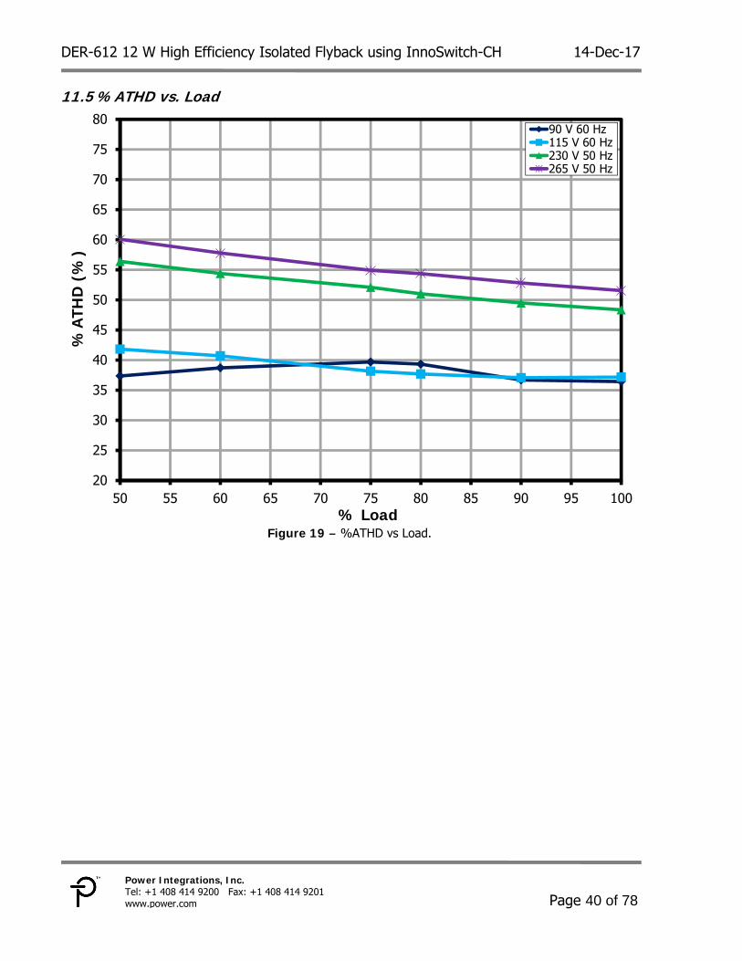
11.5 %ATHD vs. Load
Figure 19 – %ATHD vs Load.
20
25
30
35
40
45
50
55
60
65
70
75
80
50 55 60 65 70 75 80 85 90 95 100
%A
THD
(%
)
% Load
90 V 60 Hz115 V 60 Hz230 V 50 Hz265 V 50 Hz

14-Dec-17 DER-612 12 W High Efficiency Isolated Flyback using InnoSwitch-CH
Page 41 of 78
Power Integrations Tel: +1 408 414 9200 Fax: +1 408 414 9201
www.power.com
12 Thermal Performance
12.1 Thermal Scan at 25 ºC Ambient
Figure 20 – Test Set-up Picture - Open Frame
Unit in open frame was placed inside an acrylic enclosure to prevent airflow that might affect the thermal measurements. Temperature was measured using FLIR thermal camera.

DER-612 12 W High Efficiency Isolated Flyback using InnoSwitch-CH 14-Dec-17
Page 42 of 78
Power Integrations, Inc. Tel: +1 408 414 9200 Fax: +1 408 414 9201 www.power.com
12.1.1 Thermal Scan at 90 VAC Full Load
Figure 21 – 90 VAC 60 Hz, Full Load. InnoSwitch-CH (U1): 49.7 ºC.
Figure 22 – 90 VAC 60 Hz, Full Load. Output Diode (D7): 51.9 ºC.
Figure 23 – 90 VAC 60 Hz, Full Load. Power Transformer (T1): 46.7 ºC.
Figure 24 – 90 VAC 60 Hz, Full Load. Inductor (L2): 63.1 ºC.

14-Dec-17 DER-612 12 W High Efficiency Isolated Flyback using InnoSwitch-CH
Page 43 of 78
Power Integrations Tel: +1 408 414 9200 Fax: +1 408 414 9201
www.power.com
12.1.2 Thermal Scan at 115 VAC Full Load
Figure 25 – 115 VAC 60 Hz, Full Load. InnoSwitch-CH (U1): 47.5 ºC
Figure 26 – 115 VAC 60 Hz, Full Load. Output Diode (D7): 51.9 ºC.
Figure 27 – 115 VAC 60 Hz, Full Load. Power Transformer (T1): 48.3 ºC.
Figure 28 – 115 VAC 60 Hz, Full Load. Inductor (L2): 48 ºC.
DER-612 12 W High Efficiency Isolated Flyback using InnoSwitch-CH 14-Dec-17
Page 44 of 78
Power Integrations, Inc. Tel: +1 408 414 9200 Fax: +1 408 414 9201 www.power.com
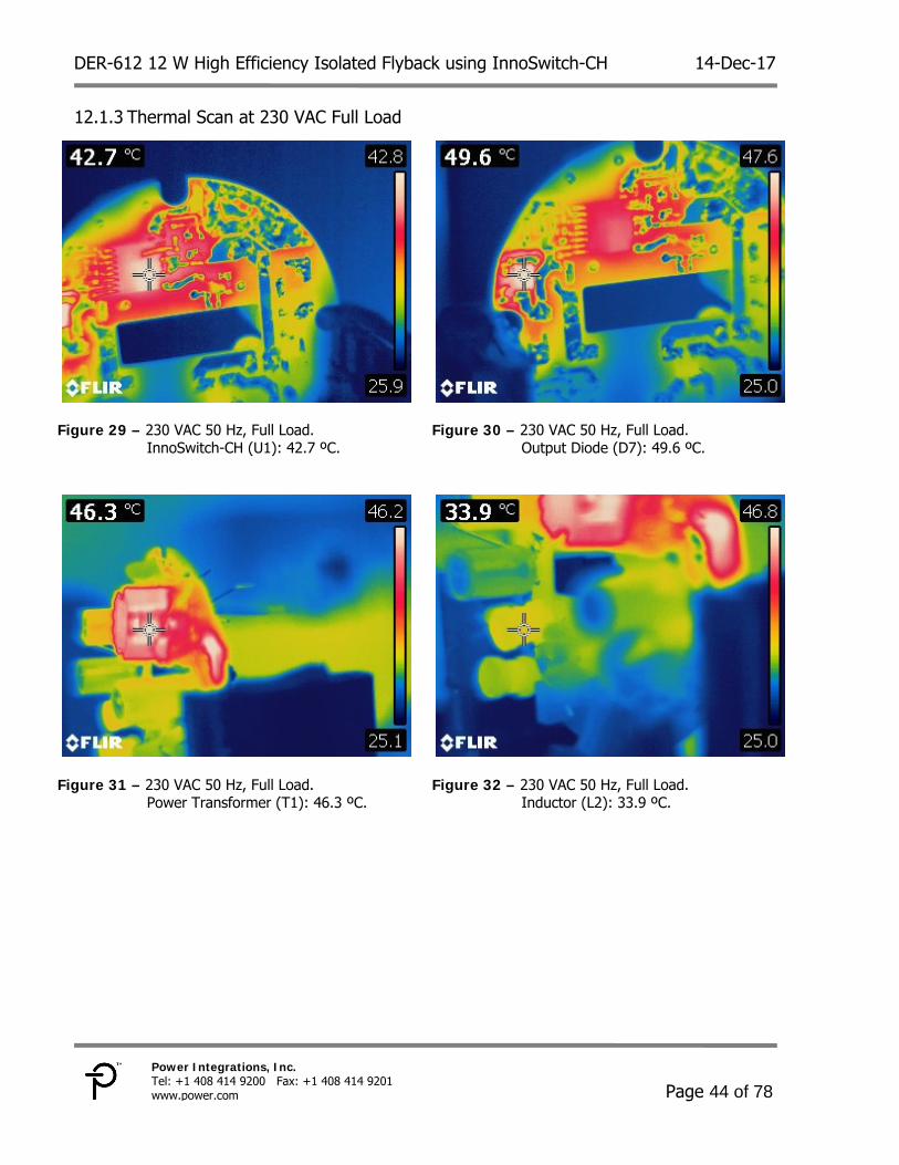
12.1.3 Thermal Scan at 230 VAC Full Load
Figure 29 – 230 VAC 50 Hz, Full Load. InnoSwitch-CH (U1): 42.7 ºC.
Figure 30 – 230 VAC 50 Hz, Full Load. Output Diode (D7): 49.6 ºC.
Figure 31 – 230 VAC 50 Hz, Full Load. Power Transformer (T1): 46.3 ºC.
Figure 32 – 230 VAC 50 Hz, Full Load. Inductor (L2): 33.9 ºC.

14-Dec-17 DER-612 12 W High Efficiency Isolated Flyback using InnoSwitch-CH
Page 45 of 78
Power Integrations Tel: +1 408 414 9200 Fax: +1 408 414 9201
www.power.com
12.1.4 Thermal Scan at 265 VAC Full Load
Figure 33 – 265 VAC 50 Hz, Full Load. InnoSwitch-CH (U1): 43.8 ºC.
Figure 34 – 265 VAC 50 Hz, Full Load. Output Diode (D7): 49.7 ºC.
Figure 35 – 265 VAC 50 Hz, Full Load. Power Transformer (T1): 48 ºC.
Figure 36 – 265 VAC 50 Hz, Full Load. Inductor (L2): 33.5 ºC.

DER-612 12 W High Efficiency Isolated Flyback using InnoSwitch-CH 14-Dec-17
Page 46 of 78
Power Integrations, Inc. Tel: +1 408 414 9200 Fax: +1 408 414 9201 www.power.com
12.2 Thermal Test at 75 0C Ambient
Set-up: Unit: DER-612 open frame Test Chamber: Tenney Ambient Temperature: 75 ºC (inside enclosure) Data Logger: Yokogawa Thermocouple: Type T
Figure 37 – Test Set-up Pictures. Unit is placed inside an enclosure to prevent the effect of airflow.

14-Dec-17 DER-612 12 W High Efficiency Isolated Flyback using InnoSwitch-CH
Page 47 of 78
Power Integrations Tel: +1 408 414 9200 Fax: +1 408 414 9201
www.power.com
12.3 Thermal Test Data at 75 ºC Ambient
12.4 Electrical Test Data at 75 ºC Ambient Input Input Measurement Load Measurement
Efficiency (%) VAC
(VRMS) Freq (Hz)
VIN (VRMS)
IIN (ARMS)
PIN (W) PF %ATHD VOUT
(VDC) IOUT
(ADC) POUT (W)
90 60 89.90 0.18 14.96 0.929 31.22 30.13 0.40 12.03 80.42 100 60 99.86 0.17 15.05 0.904 34.72 30.43 0.40 12.15 80.74 115 60 114.89 0.14 14.78 0.902 37.10 30.54 0.40 12.20 82.56 120 60 119.87 0.14 14.63 0.900 38.06 30.54 0.40 12.20 83.36 132 60 131.88 0.12 14.39 0.897 38.56 30.56 0.40 12.20 84.79 185 50 184.89 0.09 13.89 0.883 43.37 30.56 0.40 12.20 87.84 200 50 199.91 0.08 13.82 0.871 45.17 30.57 0.40 12.21 88.32 230 50 229.92 0.07 13.73 0.849 47.97 30.59 0.40 12.21 88.91 240 50 239.96 0.07 13.71 0.840 48.82 30.59 0.40 12.21 89.07 265 50 264.94 0.06 13.70 0.820 51.40 30.59 0.40 12.22 89.21
Item Description Thermal Data (ºC)
90 V 115 V 230 V 265 V 1 Ambient 75.7 76.3 75.3 75.4 2 U1 - InnoSwitch-CH 107 105.2 95 95.2 3 C3 - BulK Capacitor 89.4 90.5 82.8 81.9 4 T1 - Transformer 99.7 99.9 96.5 95.9 5 L1 - Differential Choke 120 105.8 84 82.8 6 R7 - Current Limiting Resistor 96.4 100.9 85.8 84.7 7 D7 - Output Diode 101.1 101.2 97.9 97.6 8 C10 - Output Capacitor 86.2 86.4 84.3 84.4 9 D3 - Charging Diode 93.2 93 82.8 82.1

DER-612 12 W High Efficiency Isolated Flyback using InnoSwitch-CH 14-Dec-17
Page 48 of 78
Power Integrations, Inc. Tel: +1 408 414 9200 Fax: +1 408 414 9201 www.power.com
13 Waveforms Waveforms were taken at room temperature (25 ºC)
13.1 Input Voltage and Input Current at Full Load
Figure 38 –90 VAC 60 Hz, Full Load.
Upper: IIN, 200 mA / div. Lower: VIN, 100 V / div., 10 ms / div.
Figure 39 – 115 VAC 60 Hz, Full Load. Upper: IIN, 100 mA / div. Lower: VIN, 100 V / div., 10 ms / div.
Figure 40 – 230 VAC 50 Hz, Full Load.
Upper: IIN, 50 mA / div. Lower: VIN, 100 V / div., 10 ms / div.
Figure 41 – 265 VAC 50 Hz, Full Load. Upper: IIN, 50 mA / div. Lower: VIN, 100 V / div., 10 ms / div.

14-Dec-17 DER-612 12 W High Efficiency Isolated Flyback using InnoSwitch-CH
Page 49 of 78
Power Integrations Tel: +1 408 414 9200 Fax: +1 408 414 9201
www.power.com
13.2 Start-up Profile at Full Load
Figure 42 – 90 VAC 60 Hz, Full Load Start-up.
Upper: VOUT, 5 V / div. Lower: VIN, 100 V / div., 50 ms / div.
Turn-on Time: 46 ms.
Figure 43 – 115 VAC 60 Hz, Full Load Start-up. Upper: VOUT, 5 V / div. Lower: VIN, 100 V / div., 50 ms / div.
Turn-on Time: 40 ms.
Figure 44 – 230 VAC 50 Hz, Full Load Start-up.
Upper: VOUT, 5 V / div. Lower: VIN, 100 V / div., 50 ms / div.
Turn-on Time: 26 ms.
Figure 45 – 265 VAC 50 Hz, Full Load Start-up. Upper: VOUT, 5 V / div. Lower: VIN, 100 V / div., 50 ms / div.
Turn-on Time: 25 ms

DER-612 12 W High Efficiency Isolated Flyback using InnoSwitch-CH 14-Dec-17
Page 50 of 78
Power Integrations, Inc. Tel: +1 408 414 9200 Fax: +1 408 414 9201 www.power.com
13.3 Output Voltage Fall
Figure 46 – 90 VAC 60 Hz, Full Load, Output Fall.
Upper: VOUT, 5 V / div. Lower: VIN, 100 V / div., 50 ms / div.
Figure 47 – 115 VAC 60 Hz, Full Load, Output Fall. Upper: VOUT, 5 V / div. Lower: VIN, 100 V / div., 50 ms / div.
Figure 48 – 230 VAC 50 Hz, Full Load, Output Fall.
Upper: VOUT, 5 V / div. Lower: VIN, 100 V / div., 50 ms / div. Hold-up Time: 53 ms.
Figure 49 – 265 VAC 50 Hz, Full Load, Output Fall. Upper: VOUT, 5 V / div. Lower: VIN, 100 V / div., 50 ms / div.
Hold-up Time: 74 ms.
14-Dec-17 DER-612 12 W High Efficiency Isolated Flyback using InnoSwitch-CH
Page 51 of 78
Power Integrations Tel: +1 408 414 9200 Fax: +1 408 414 9201
www.power.com
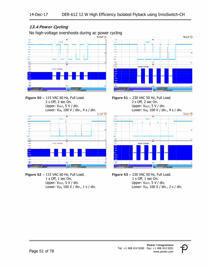
13.4 Power Cycling No high-voltage overshoots during ac power cycling
Figure 50 – 115 VAC 60 Hz, Full Load.
2 s Off, 2 sec On. Upper: VOUT, 5 V / div. Lower: VIN, 100 V / div., 4 s / div.
Figure 51 – 230 VAC 50 Hz, Full Load. 2 s Off, 2 sec On. Upper: VOUT, 5 V / div. Lower: VIN, 100 V / div., 4 s / div.
Figure 52 – 115 VAC 60 Hz, Full Load. 1 s Off, 1 sec On.
Upper: VOUT, 5 V / div. Lower: VIN, 100 V / div., 1 s / div.
Figure 53 – 230 VAC 50 Hz, Full Load. 1 s Off, 1 sec On.
Upper: VOUT, 5 V / div. Lower: VIN, 100 V / div., 2 s / div.

DER-612 12 W High Efficiency Isolated Flyback using InnoSwitch-CH 14-Dec-17
Page 52 of 78
Power Integrations, Inc. Tel: +1 408 414 9200 Fax: +1 408 414 9201 www.power.com
13.5 Load Transient Response 3 Hz
Figure 54 – 115 VAC 60 Hz. 0% to 100% Load Change. 3 Hz, 50% Duty Cycle. Slew Rate: 800 mA / S.
Upper: VOUT, 5 V / div., 100 ms / div. Lower: IOUT, 100 mA / div.
Figure 55 – 230 VAC 50 Hz. 0% to 100% Load Change. 3 Hz, 50% Duty Cycle. Slew Rate: 800 mA / S.
Upper: VOUT, 5 V / div., 100 ms / div. Lower: Iout, 100 mA / div.
Figure 56 – 115 VAC 60 Hz. 50% to 100% Load Change. 3 Hz, 50% Duty Cycle. Slew Rate: 800 mA / S.
Upper: VOUT, 5 V / div., 100 ms / div. Lower: IOUT, 100 mA / div.
Figure 57 – 230 VAC 50 Hz. 50% to 100% Load Change. 3 Hz, 50% Duty Cycle. Slew Rate: 800 mA / S.
Upper: VOUT, 5 V / div., 100 ms / div. Lower: IOUT, 100 mA / div.

14-Dec-17 DER-612 12 W High Efficiency Isolated Flyback using InnoSwitch-CH
Page 53 of 78
Power Integrations Tel: +1 408 414 9200 Fax: +1 408 414 9201
www.power.com
13.6 Load Transient Response 100 Hz
Figure 58 – 115 VAC 60 Hz. 0% to 100% Load Change. 100 Hz, 50% Duty Cycle. Slew Rate: 800 mA / S.
Upper: VOUT, 5 V / div., 4 ms / div. Lower: IOUT, 100 mA / div.
Figure 59 – 230 VAC 50 Hz. 0% to 100% Load Change. 100 Hz, 50% Duty Cycle. Slew Rate: 800 mA / S.
Upper: VOUT, 5 V / div., 4 ms / div. Lower: IOUT, 100 mA / div.
Figure 60 – 115 VAC 60 Hz. 50% to 100% Load Change. 100 Hz, 50% Duty Cycle. Slew Rate: 800 mA / S.
Upper: VOUT, 5 V / div., 4 ms / div. Lower: IOUT, 100 mA / div.
Figure 61 – 230 VAC 50 Hz, Full Load. 50% to 100% Load Change. 100 Hz, 50% Duty Cycle. Slew Rate: 800 mA / S.
Upper: VOUT, 5 V / div., 4 ms / div. Lower: IOUT, 100 mA / div.

DER-612 12 W High Efficiency Isolated Flyback using InnoSwitch-CH 14-Dec-17
Page 54 of 78
Power Integrations, Inc. Tel: +1 408 414 9200 Fax: +1 408 414 9201 www.power.com
13.7 InnoSwitch-CH Drain Voltage and Current Waveforms
Figure 62 – 90 VAC 60 Hz, Full Load Normal.
Upper: IDRAIN, 200 mA / div. Lower: VDRAIN, 50 V / div., 4 ms / div.
Figure 63 – 90 VAC 60 Hz, Full Load Normal. Upper: IDRAIN, 200 mA / div. Lower: VDRAIN, 50 V / div., 10 s / div.
Figure 64 – 115 VAC 60 Hz, Full Load Normal.
Upper: IDRAIN, 200 mA / div. Lower: VDRAIN, 50 V / div., 4 ms / div.
Figure 65 – 115 VAC 60 Hz, Full Load Normal. Upper: IDRAIN, 200 mA / div. Lower: VDRAIN, 50 V / div., 10 s / div.

14-Dec-17 DER-612 12 W High Efficiency Isolated Flyback using InnoSwitch-CH
Page 55 of 78
Power Integrations Tel: +1 408 414 9200 Fax: +1 408 414 9201
www.power.com
Figure 66 – 230 VAC 50 Hz, Full Load Normal.
Upper: IDRAIN, 200 mA / div. Lower: VDRAIN, 100 V / div., 4 ms / div.
Figure 67 – 230 VAC 50 Hz, Full Load Normal Upper: IDRAIN, 200 mA / div. Lower: VDRAIN, 100 V / div., 10 s / div.
Figure 68 – 265 VAC 50 Hz, Full Load Normal. Upper: IDRAIN, 200 mA / div. Lower: VDRAIN, 100 V / div., 4 ms / div.
Figure 69 – 265 VAC, Full Load Normal. Upper: IDRAIN, 200 mA / div. Lower: VDRAIN, 100 V / div., 10 s / div.
DER-612 12 W High Efficiency Isolated Flyback using InnoSwitch-CH 14-Dec-17
Page 56 of 78
Power Integrations, Inc. Tel: +1 408 414 9200 Fax: +1 408 414 9201 www.power.com
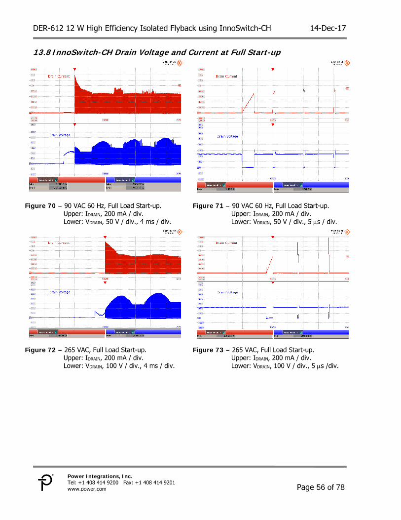
13.8 InnoSwitch-CH Drain Voltage and Current at Full Start-up
Figure 70 – 90 VAC 60 Hz, Full Load Start-up.
Upper: IDRAIN, 200 mA / div. Lower: VDRAIN, 50 V / div., 4 ms / div.
Figure 71 – 90 VAC 60 Hz, Full Load Start-up. Upper: IDRAIN, 200 mA / div. Lower: VDRAIN, 50 V / div., 5 s / div.
Figure 72 – 265 VAC, Full Load Start-up.
Upper: IDRAIN, 200 mA / div. Lower: VDRAIN, 100 V / div., 4 ms / div.
Figure 73 – 265 VAC, Full Load Start-up. Upper: IDRAIN, 200 mA / div. Lower: VDRAIN, 100 V / div., 5 s /div.
14-Dec-17 DER-612 12 W High Efficiency Isolated Flyback using InnoSwitch-CH
Page 57 of 78
Power Integrations Tel: +1 408 414 9200 Fax: +1 408 414 9201
www.power.com
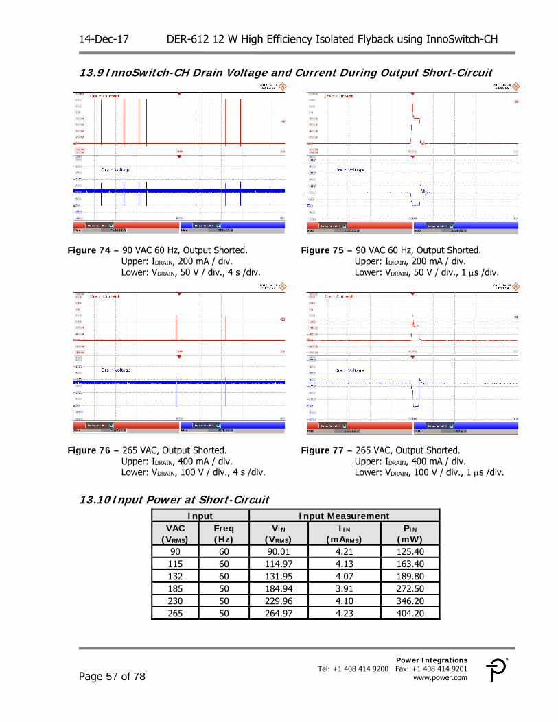
13.9 InnoSwitch-CH Drain Voltage and Current During Output Short-Circuit
Figure 74 – 90 VAC 60 Hz, Output Shorted.
Upper: IDRAIN, 200 mA / div. Lower: VDRAIN, 50 V / div., 4 s /div.
Figure 75 – 90 VAC 60 Hz, Output Shorted. Upper: IDRAIN, 200 mA / div. Lower: VDRAIN, 50 V / div., 1 s /div.
Figure 76 – 265 VAC, Output Shorted.
Upper: IDRAIN, 400 mA / div. Lower: VDRAIN, 100 V / div., 4 s /div.
Figure 77 – 265 VAC, Output Shorted. Upper: IDRAIN, 400 mA / div. Lower: VDRAIN, 100 V / div., 1 s /div.
13.10 Input Power at Short-Circuit Input Input Measurement
VAC (VRMS)
Freq (Hz)
VIN (VRMS)
IIN (mARMS)
PIN (mW)
90 60 90.01 4.21 125.40 115 60 114.97 4.13 163.40 132 60 131.95 4.07 189.80 185 50 184.94 3.91 272.50 230 50 229.96 4.10 346.20 265 50 264.97 4.23 404.20

DER-612 12 W High Efficiency Isolated Flyback using InnoSwitch-CH 14-Dec-17
Page 58 of 78
Power Integrations, Inc. Tel: +1 408 414 9200 Fax: +1 408 414 9201 www.power.com
13.11 Output Ripple Voltage
Figure 78 – 90 VAC 60 Hz, Full Load.
AC Coupling, 20 MHz Bandwidth. VOUT, 100 mV / div., 10 ms / div. Ripple Voltage: 648.2 mVP-P.
Figure 79 – 115 VAC 60 Hz, Full Load. AC Coupling, 20 MHz Bandwidth. VOUT, 20 mV / div., 10 ms / div. Ripple Voltage: 122.53 mVP-P.
Figure 80 – 230 VAC 50 Hz, Full Load.
AC Coupling, 20 MHz Bandwidth. VOUT, 20 mV / div., 10 ms / div. Ripple Voltage: 122.53 mVP-P.
Figure 81 – 265 VAC 50 Hz, Full Load. AC Coupling, 20 MHz Bandwidth. VOUT, 20 mV / div., 10 ms / div. Ripple Voltage: 132.8 mVP-P.

14-Dec-17 DER-612 12 W High Efficiency Isolated Flyback using InnoSwitch-CH
Page 59 of 78
Power Integrations Tel: +1 408 414 9200 Fax: +1 408 414 9201
www.power.com
14 Conducted EMI
14.1 Test Set-up Unit is placed on top of load metal chassis.
14.2 Equipment and Load Used 1. Rohde and Schwarz ENV216 two line V-network. 2. Rohde and Schwarz ESRP EMI test receiver. 3. Hioki 3322 power hitester. 4. Chroma measurement test fixture. 5. Full Load with input voltage set at 115 VAC 60 Hz and 230 VAC 60 Hz.
Figure 82 – Conducted EMI Test Set-up.
DER-612 12 W High Efficiency Isolated Flyback using InnoSwitch-CH 14-Dec-17
Page 60 of 78
Power Integrations, Inc. Tel: +1 408 414 9200 Fax: +1 408 414 9201 www.power.com
14.3 EMI Test Result
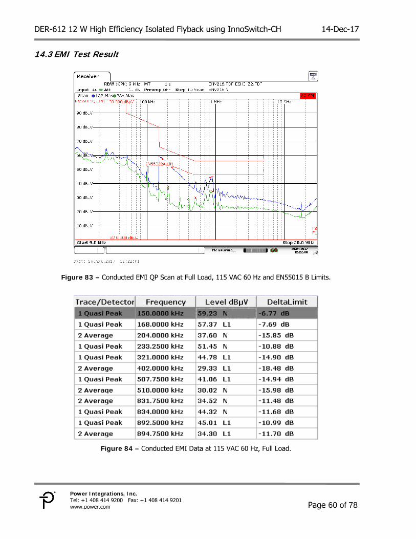
Figure 83 – Conducted EMI QP Scan at Full Load, 115 VAC 60 Hz and EN55015 B Limits.
Figure 84 – Conducted EMI Data at 115 VAC 60 Hz, Full Load.

14-Dec-17 DER-612 12 W High Efficiency Isolated Flyback using InnoSwitch-CH
Page 61 of 78
Power Integrations Tel: +1 408 414 9200 Fax: +1 408 414 9201
www.power.com
Figure 85 – Conducted EMI QP Scan at Full Load, 230 VAC 60 Hz and EN55015 B Limits.
Figure 86 – Conducted EMI Data at 230 VAC 60 Hz, Full Load.
DER-612 12 W High Efficiency Isolated Flyback using InnoSwitch-CH 14-Dec-17
Page 62 of 78
Power Integrations, Inc. Tel: +1 408 414 9200 Fax: +1 408 414 9201 www.power.com
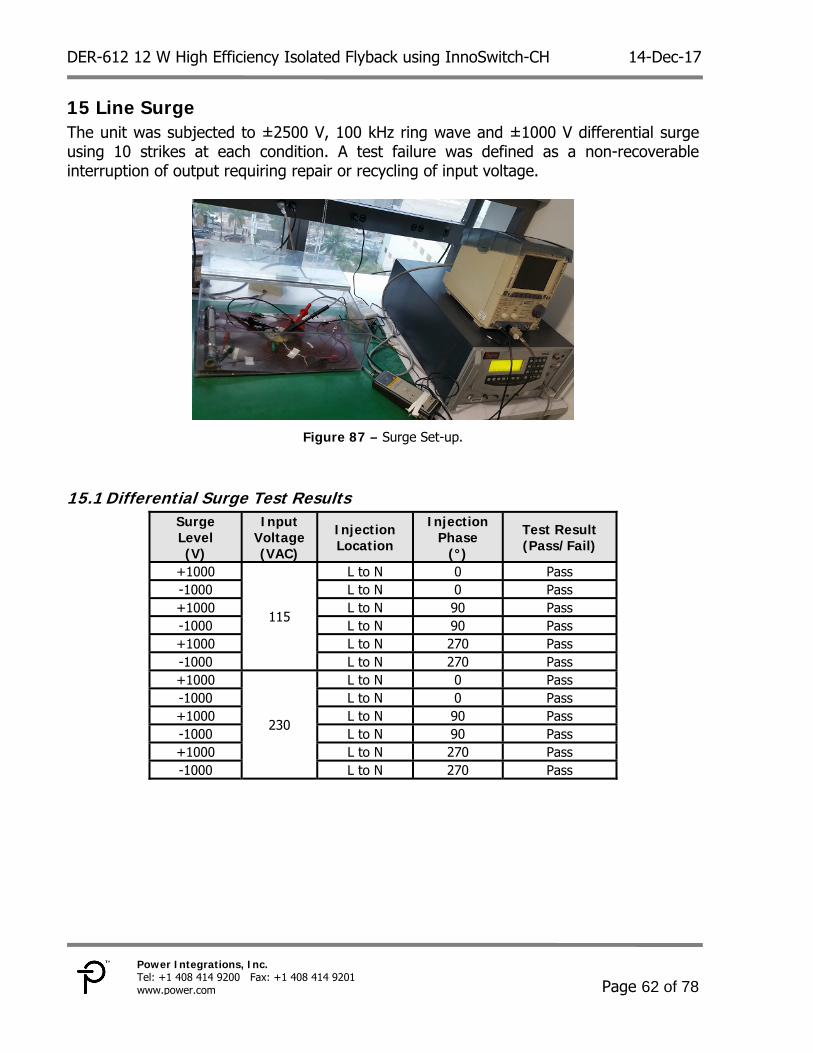
15 Line Surge The unit was subjected to ±2500 V, 100 kHz ring wave and ±1000 V differential surge using 10 strikes at each condition. A test failure was defined as a non-recoverable interruption of output requiring repair or recycling of input voltage.
Figure 87 – Surge Set-up.
15.1 Differential Surge Test Results Surge Level (V)
Input Voltage (VAC)
Injection Location
Injection Phase
(°)
Test Result (Pass/Fail)
+1000
115
L to N 0 Pass -1000 L to N 0 Pass +1000 L to N 90 Pass -1000 L to N 90 Pass +1000 L to N 270 Pass -1000 L to N 270 Pass +1000
230
L to N 0 Pass -1000 L to N 0 Pass +1000 L to N 90 Pass -1000 L to N 90 Pass +1000 L to N 270 Pass -1000 L to N 270 Pass
14-Dec-17 DER-612 12 W High Efficiency Isolated Flyback using InnoSwitch-CH
Page 63 of 78
Power Integrations Tel: +1 408 414 9200 Fax: +1 408 414 9201
www.power.com
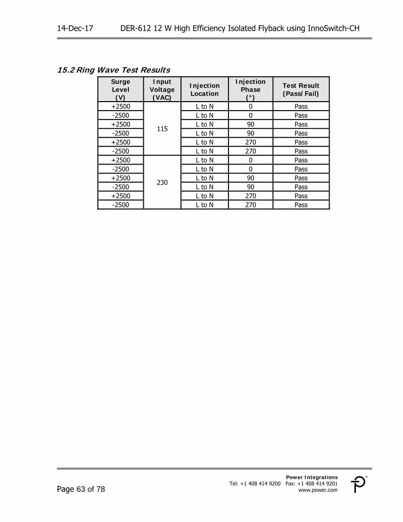
15.2 Ring Wave Test Results Surge Level (V)
Input Voltage (VAC)
Injection Location
Injection Phase
(°)
Test Result (Pass/Fail)
+2500
115
L to N 0 Pass -2500 L to N 0 Pass +2500 L to N 90 Pass -2500 L to N 90 Pass +2500 L to N 270 Pass -2500 L to N 270 Pass +2500
230
L to N 0 Pass -2500 L to N 0 Pass +2500 L to N 90 Pass -2500 L to N 90 Pass +2500 L to N 270 Pass -2500 L to N 270 Pass

DER-612 12 W High Efficiency Isolated Flyback using InnoSwitch-CH 14-Dec-17
Page 64 of 78
Power Integrations, Inc. Tel: +1 408 414 9200 Fax: +1 408 414 9201 www.power.com
15.3 Differential Surge (1 KV) The Drain voltage of InnoSwitch-CH was measured during 1 kV differential surge test.
Figure 88 – (-)1 kV Differential Surge.
VIN=230 V, 90º Phase Angle. Lower: VDRAIN, 200 V / div., 10 ms / div. Peak VDRAIN: 516.67 V.
Figure 89 – (+)1 kV Differential Surge. VIN = 230 V, 90º Phase Angle. Lower: VDRAIN, 200 V / div., 10 ms / div. Peak VDRAIN: 508.33 V.
15.4 Ring Wave Test (2.5 kV) The Drain voltage of InnoSwitch-CH was measured during 2.5 kV ring wave test.
Figure 90 – (+)2.5 kV Ring Wave.
VIN = 230 V, 90º Phase Angle. Lower: VDRAIN, 200 V / div., 10 ms / div. Peak VDRAIN: 483.33 V.
Figure 91 – (-)2.5 kV Ring Wave Surge. VIN = 230 V, 90º Phase Angle. Lower: VDRAIN, 200 V / div., 10 ms / div. Peak VDRAIN: 450 V.

14-Dec-17 DER-612 12 W High Efficiency Isolated Flyback using InnoSwitch-CH
Page 65 of 78
Power Integrations Tel: +1 408 414 9200 Fax: +1 408 414 9201
www.power.com
16 Brown-in/Brown-out Test No abnormal overheating or voltage overshoot / undershoot was observed during and after 0.5 V / s and 1 V / s brown-in and brown-out test.
Figure 92 – Brown-in Test at 0.5 V / s.
Ch1: VOUT, 5 V / div. Ch2: VIN, 100 V / div. Time Scale: 50 s / div.
Figure 93 – Brown-out Test at 0.5 V / s. Ch1: VOUT, 5 V / div. Ch2: VIN, 100 V / div. Time Scale: 50 s / div.
Figure 94 – Brown-in Test at 1 V / s.
Ch1: VOUT, 5 V / div. Ch2: VIN, 100 V / div. Time Scale: 50 s / div.
Figure 95 – Brown-out Test at 1 V / s. Ch1: VOUT, 5 V /div. Ch2: VIN, 100 V / div. Time Scale: 50 s / div.

DER-612 12 W High Efficiency Isolated Flyback using InnoSwitch-CH 14-Dec-17
Page 66 of 78
Power Integrations, Inc. Tel: +1 408 414 9200 Fax: +1 408 414 9201 www.power.com
17 Appendix
17.1 Application Example
17.1.1 Smart RGBW Downlight with BLE Control In this application, DER-612 is used to power a smart RGBW LED downlight controlled via Bluetooth Low Energy (BLE) module. The BLE module used is the Casambi CBM-001.
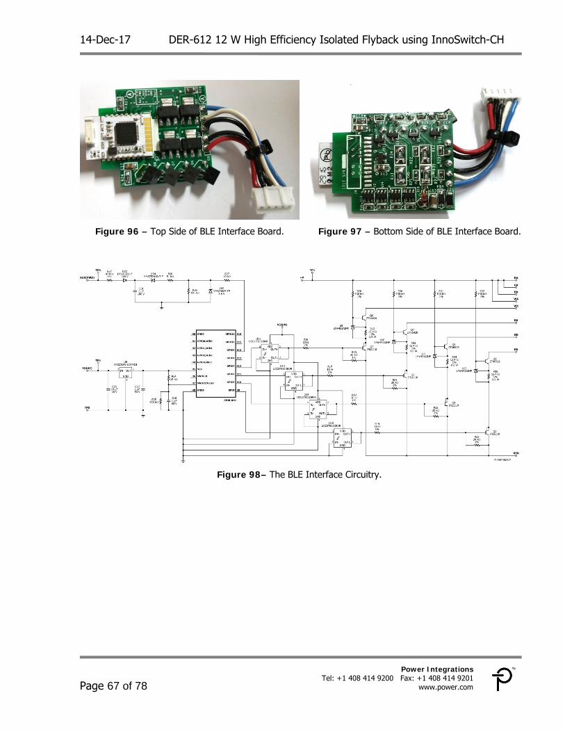
17.1.2 BLE Interface Circuitry The BLE Interface Circuitry consists of a 3.3 V linear regulator, the Zero Detect circuit, the Casambi CBM-001 Bluetooth Low Energy (BLE) module, the PWM-driven MOSFETs, and the constant current circuit for each string of the RGBW LED Load. Figure 96 shows the BLE Interface Circuitry. U6 is the 3.3 V linear regulator with input and output bypass capacitors C16 and C17, respectively. The output of the 3.3 V regulator is connected to the VCC pin of the Casambi CBM-001 module (U8). R24, R25, and C18 compose the Power-On Reset (POR) circuitry required for the BLE module. The BLE module also requires a means to detect when the input turns OFF (Zero Detect circuitry). The signal coming from the secondary auxiliary forward winding is rectified by D22 and filtered by C19, then clamped by VR5 for this purpose. C19 must be sized just enough to average the rectified signal and filter noise, as it has to discharge quickly when the input turns OFF. R37 forms an RC filter with C19 that helps minimize the unwanted noise from the forward winding signal. R26 and R27 are current limiters. When the input turns OFF, the C19 voltage will be equal to that of C8 of DER-612; to immediately cut the signal from the set Zero Detect pin of the BLE module (GPIO9, in this case), VR4 voltage is set just above the steady-state voltage of C8. R36 also helps for faster decay of the signal from the Zero Detect pin of the BLE module. Refer to Casambi CBM-001 datasheet for more details on POR and Zero Detect functionalities. U13, U14, U15, and U16 are gate drivers with PWM inputs coming from the BLE module, and PWM outputs driving the gates of Q2, Q3, Q4, and Q5 through gate resistors R16, R17, R18, and R19, respectively. There’s a constant current circuit for each of the LED string – Q6, U9, and R12 for White LED string; Q7, U10, and R33 for Blue LED string; Q8, U11, and R34 for Green LED string; and Q9, U12, and R35 for Red LED string. The voltages across R12, R33, R34, and R35 are maintained constant by the LMV431 regulators U9, U10, U11, and U12 when the MOSFETs are conducting; hence, the emitter current (as well as the collector current, and therefore, the LED maximum current) is also constant. The LED current for each string is thereby averaged through the set PWM duty; hence, the resulting output color, the brightness, and the color temperature could be set by varying the duty cycle for each of the RGBW LED string. R28, R30, R31, and R32 are base resistors for biasing the BJTs and the LMV431 regulators. The current gain of the BJTs and the desired maximum current for the LED strings should be considered when calculating the value of these base resistors.
14-Dec-17 DER-612 12 W High Efficiency Isolated Flyback using InnoSwitch-CH
Page 67 of 78
Power Integrations Tel: +1 408 414 9200 Fax: +1 408 414 9201
www.power.com
Figure 96 – Top Side of BLE Interface Board. Figure 97 – Bottom Side of BLE Interface Board.
Figure 98– The BLE Interface Circuitry.

DER-612 12 W High Efficiency Isolated Flyback using InnoSwitch-CH 14-Dec-17
Page 68 of 78
Power Integrations, Inc. Tel: +1 408 414 9200 Fax: +1 408 414 9201 www.power.com
Figure 99 – BLE Interface Board: Component Side.

14-Dec-17 DER-612 12 W High Efficiency Isolated Flyback using InnoSwitch-CH
Page 69 of 78
Power Integrations Tel: +1 408 414 9200 Fax: +1 408 414 9201
www.power.com
Figure 100 – BLE Interface Board: Second Layer.
Figure 101 – BLE Interface Board: Third Layer.

DER-612 12 W High Efficiency Isolated Flyback using InnoSwitch-CH 14-Dec-17
Page 70 of 78
Power Integrations, Inc. Tel: +1 408 414 9200 Fax: +1 408 414 9201 www.power.com
Figure 102 – BLE Interface Board: Solder Side.
17.2 RGBW LED Load Engine The RGBW LED Load circuitry is shown on Figure 101. It is composed of twelve single-package RGBW LEDs, arrange in a way so as to optimize the string voltage of each color; that is, the total voltage of each string must be as close as possible to each other. This is why the Red LED string is comprised of 12 LEDs plus a diode in series; the Green LED string is comprised of 8 LEDs plus diode in series; and the Blue and White LED strings are comprised of 9 LEDs. This optimization is done to minimize the power loss of the BJTs on the constant-current circuit. The arrangement of the LEDs on the PCB board should also be considered so as to achieve a distributed light output and make the blending of colors more effective.

14-Dec-17 DER-612 12 W High Efficiency Isolated Flyback using InnoSwitch-CH
Page 71 of 78
Power Integrations Tel: +1 408 414 9200 Fax: +1 408 414 9201
www.power.com
Figure 103 – RGBW LED Engine - Top Side. Figure 104 – RGBW LED Engine - Bottom Side.
Figure 105 – The RGBW LED Load Engine.

DER-612 12 W High Efficiency Isolated Flyback using InnoSwitch-CH 14-Dec-17
Page 72 of 78
Power Integrations, Inc. Tel: +1 408 414 9200 Fax: +1 408 414 9201 www.power.com
Figure 106 – RGBW LED Board: Component Side.
Figure 107 – RGBW LED Board: Solder Side.

14-Dec-17 DER-612 12 W High Efficiency Isolated Flyback using InnoSwitch-CH
Page 73 of 78
Power Integrations Tel: +1 408 414 9200 Fax: +1 408 414 9201
www.power.com
17.3 How to Configure the Casambi CBM-001 Module The CBM-001 module is pre-loaded with the Casambi firmware in the default configuration. To view and control the module, power it up (per the reference design) and download the Casambi App to an Android from Google Play or to an iOS device from Apple’s App store. When using the Casambi app on your mobile device in proximity to the module, the module will appear on the “Nearby devices” list inside the Casambi App. Follow the onscreen instructions to create a network and add your module to this network. The module will appear on the Luminaires tab within the Casambi app. You can interact with the module in at least 4 ways:
- A single tap on the module icon toggles all channels on or off - Dragging your finger across the module icon from left to right increases the
brightness level - A double tap on the module icon brings up a popup screen providing additional
information about the module - A long press on the module icon brings up a popup screen which allows adjustment of
individual channels. Additional information about using Casambi as well as technical information on the CBM-001 can be found on WWW.Casambi.com Casambi provides tools to modify the firmware if your design requires it. Modifying the firmware consists of two steps. The first step is using the Casambi web portal to create a downloadable file. This web portal is menu driven. The second step is to use Casambi’s Utility app to load the new firmware over the air into the module. These tools require a user ID and password issued by Casambi. An account can be requested by sending an email to [email protected]. Please provide your company name, address and website, your contact information and title and a brief description of your development project. You will then receive an invitation to log into Admin.Casambi.com. Inside Casambi’s admin website, there is a “Downloads” tab where the datasheet, technical guides, and user guides can be found. Please refer to the CBM-001 datasheet, the Technical Guide CBM Module Configuration tool, and the Technical Guide Utility app for information on how to modify the module firmware and then upload that configuration to the module. An iOS device is required to upload the module configuration into the module as the Casambi Utility App (separate from the Casambi App) only supports iOS devices. It requires iOS 8.2 or later.

DER-612 12 W High Efficiency Isolated Flyback using InnoSwitch-CH 14-Dec-17
Page 74 of 78
Power Integrations, Inc. Tel: +1 408 414 9200 Fax: +1 408 414 9201 www.power.com
17.4 Complete Assembly of the Application Example
Figure 108 – Completely Assembled Downlight.
Figure 109 – RGBW Light Engine Mounted on the Downlight Housing / Heat Sink.
Figure 110 – Main Driver and BLE Interface Boards Mounted on the Downlight Housing / Heat Sink.

14-Dec-17 DER-612 12 W High Efficiency Isolated Flyback using InnoSwitch-CH
Page 75 of 78
Power Integrations Tel: +1 408 414 9200 Fax: +1 408 414 9201
www.power.com
17.5 Bill of Materials – BLE Interface Circuitry Item Qty Ref Description Mfg Part Number Mfg
1 1 C16 10 F, ±10%, 16V, X7R, Ceramic Capacitor, -55°C ~ 125°C, 0805 CL21B106KOQNNNE Samsung
2 1 C17 1 F,50 V, Ceramic, X7R, 0805 C2012X7R1H105M085AC TDK 3 1 C18 1 F,50 V, Ceramic, X7R, 0805 C2012X7R1H105M085AC TDK 4 1 C19 1 F,100 V, Ceramic, X7R, 1206 HMK316B7105KL-T Taiyo Yuden 5 1 D22 200 V, 1 A, Rectifier, Glass Passivated, POWERDI123 DFLR1200-7 Diodes, Inc.
6 1 J4 12 positions, Horizontal, Female, Header, Connector, 0.050" (1.27mm), SMD, Gold Y02443-0112CNG1ZUT01 Yinghua
7 1 Q2 MOSFET, N-Channel, 100 V, 1.5 A (Tc), 2 W (Ta), 3.1 W (Tc), 540 m @ 900 mA @ 5 V, -55°C ~ 150°C (TJ), SOT-223
IRLL110TRPBF Vishay
8 1 Q3 MOSFET, N-Channel, 100 V, 1.5 A (Tc), 2 W (Ta), 3.1 W (Tc), 540 m @ 900 mA @ 5 V, -55°C ~ 150°C (TJ), SOT-223
IRLL110TRPBF Vishay
9 1 Q4 MOSFET, N-Channel, 100 V, 1.5 A (Tc), 2 W (Ta), 3.1 W (Tc), 540 m @ 900 mA @ 5 V, -55°C ~ 150°C (TJ), SOT-223
IRLL110TRPBF Vishay
10 1 Q5 MOSFET, N-Channel, 100V, 1.5A (Tc), 2W (Ta), 3.1W (Tc), 540 mOhm @ 900mA @ 5V, -55°C ~ 150°C (TJ),SOT-223
IRLL110TRPBF Vishay
11 1 Q6 NPN, Power BJT, 70 V, 1 A, TO-92 ZTX692B Zetex 12 1 Q7 NPN, Power BJT, 70 V, 1 A, TO-92 ZTX692B Zetex 13 1 Q8 NPN, Power BJT, 70 V, 1 A, TO-92 ZTX692B Zetex 14 1 Q9 NPN, Power BJT, 70 V, 1 A, TO-92 ZTX692B Zetex 15 1 R12 RES, 12.4 , ±1%, 0.5 W, ½ W, 1210 (3225 Metric) ERJ-14NF12R4U Panasonic 16 1 R16 RES, 10 , 1%, 1/16 W, Thick Film, 0603 ERJ-3EKF10R0V Panasonic 17 1 R17 RES, 10 , 1%, 1/16 W, Thick Film, 0603 ERJ-3EKF10R0V Panasonic 18 1 R18 RES, 10 , 1%, 1/16 W, Thick Film, 0603 ERJ-3EKF10R0V Panasonic 19 1 R19 RES, 10 , 1%, 1/16 W, Thick Film, 0603 ERJ-3EKF10R0V Panasonic 20 1 R20 RES, 20 k, 1%, 1/16 W, Thick Film, 0603 ERJ-3EKF2002V Panasonic 21 1 R21 RES, 20 k, 1%, 1/16 W, Thick Film, 0603 ERJ-3EKF2002V Panasonic 22 1 R22 RES, 20 k, 1%, 1/16 W, Thick Film, 0603 ERJ-3EKF2002V Panasonic 23 1 R23 RES, 20 k, 1%, 1/16 W, Thick Film, 0603 ERJ-3EKF2002V Panasonic 24 1 R24 RES, 10 k, 5%, 1/8 W, Thick Film, 0805 ERJ-6GEYJ103V Panasonic 25 1 R25 RES, 220 k, 5%, 1/8 W, Thick Film, 0805 ERJ-6GEYJ224V Panasonic 26 1 R26 RES, 51 k, 5%, 1/8 W, Thick Film, 0805 ERJ-6GEYJ513V Panasonic 27 1 R27 RES, 10 k, 5%, 1/8 W, Thick Film, 0805 ERJ-6GEYJ103V Panasonic 28 1 R28 RES, 130 k, 1%, 1/16 W, Thick Film, 0603 ERJ-3EKF1303V Panasonic 29 1 R30 RES, 130 k, 1%, 1/16 W, Thick Film, 0603 ERJ-3EKF1303V Panasonic 30 1 R31 RES, 130 k, 1%, 1/16 W, Thick Film, 0603 ERJ-3EKF1303V Panasonic 31 1 R32 RES, 130 k, 1%, 1/16 W, Thick Film, 0603 ERJ-3EKF1303V Panasonic 32 1 R33 RES, 12.4 ±1%, 0.5W, 1/2W, 1210 ERJ-14NF12R4U Panasonic 33 1 R34 RES, 12.4 , ±1%, 0.5W, 1/2W, 1210 ERJ-14NF12R4U Panasonic 34 1 R35 RES, 12.4 , ±1%, 0.5W, 1/2W, 1210 ERJ-14NF12R4U Panasonic 35 1 R36 RES, 100 k, 5%, 1/8 W, Thick Film, 0805 ERJ-6GEYJ104V Panasonic 36 1 R37 RES, 47.0 , 1%, 1/8 W, Thick Film, 0805 ERJ-6ENF47R0V Panasonic 37 1 U6 IC, REG, LDO, 3.3V, 0.3A, SOT23-3 P2210N-3.3TRG1 Diodes, Inc. 38 1 U8 RF TXRX MOD, BLUETOOTH, TRACE ANT CBM-001 Casambi 39 1 U9 1.24 V Shunt Regulator IC, 1%, -40 to 85 C, SOT23-3 LMV431AIMF National Semi 40 1 U10 1.24 V Shunt Regulator IC, 1%, -40 to 85 C, SOT23-3 LMV431AIMF National Semi 41 1 U11 1.24 V Shunt Regulator IC, 1%, -40 to 85 C, SOT23-3 LMV431AIMF National Semi 42 1 U12 1.24 V Shunt Regulator IC, 1%, -40 to 85 C, SOT23-3 LMV431AIMF National Semi 43 1 U13 IC, GATE DVR, LOW SIDE, 1CH, SOT23-6 UCC27511DBVR Texas Instruments 44 1 U14 IC, GATE DVR, LOW SIDE, 1CH, SOT23-6 UCC27511DBVR Texas Instruments 45 1 U15 IC, GATE DVR, LOW SIDE, 1CH, SOT23-6 UCC27511DBVR Texas Instruments

DER-612 12 W High Efficiency Isolated Flyback using InnoSwitch-CH 14-Dec-17
Page 76 of 78
Power Integrations, Inc. Tel: +1 408 414 9200 Fax: +1 408 414 9201 www.power.com
46 1 U16 IC, GATE DVR, LOW SIDE, 1CH, SOT23-6 UCC27511DBVR Texas Instruments 47 1 VR4 DIODE ZENER 11 V 500 MW SOD123 MMSZ5241B-7-F Diodes, Inc. 48 1 VR5 DIODE, ZENER, 3.6 V, ±5%, 500 mW, SOD123, 150°C MMSZ4685-TP Micro Commercial
17.6 Bill of Materials – RGBW LED Engine Item Qty Ref Description Mfg Part Number Mfg
1 1 D1 LED, Lighting, Color, XLamp® XM-L, Red, Green, Blue, White - Cool (RGBW), 625nm Red, 528nm Green, 458nm Blue, 6850K White, 2020 (5050 Metric)
XMLCTW-A0-0000-00C3ABB02 CREE
2 1 D2 LED, Lighting, Color, XLamp® XM-L, Red, Green, Blue, White - Cool (RGBW), 625nm Red, 528nm Green, 458nm Blue, 6850K White, 2020 (5050 Metric)
XMLCTW-A0-0000-00C3ABB02 CREE
3 1 D3 LED, Lighting, Color, XLamp® XM-L, Red, Green, Blue, White - Cool (RGBW), 625nm Red, 528nm Green, 458nm Blue, 6850K White, 2020 (5050 Metric)
XMLCTW-A0-0000-00C3ABB02 CREE
4 1 D4 LED, Lighting, Color, XLamp® XM-L, Red, Green, Blue, White - Cool (RGBW), 625nm Red, 528nm Green, 458nm Blue, 6850K White, 2020 (5050 Metric)
XMLCTW-A0-0000-00C3ABB02 CREE
5 1 D5 LED, Lighting, Color, XLamp® XM-L, Red, Green, Blue, White - Cool (RGBW), 625nm Red, 528nm Green, 458nm Blue, 6850K White, 2020 (5050 Metric)
XMLCTW-A0-0000-00C3ABB02 CREE
6 1 D6 LED, Lighting, Color, XLamp® XM-L, Red, Green, Blue, White - Cool (RGBW), 625nm Red, 528nm Green, 458nm Blue, 6850K White, 2020 (5050 Metric)
XMLCTW-A0-0000-00C3ABB02 CREE
7 1 D7 LED, Lighting, Color, XLamp® XM-L, Red, Green, Blue, White - Cool (RGBW), 625nm Red, 528nm Green, 458nm Blue, 6850K White, 2020 (5050 Metric)
XMLCTW-A0-0000-00C3ABB02 CREE
8 1 D8 LED, Lighting, Color, XLamp® XM-L, Red, Green, Blue, White - Cool (RGBW), 625nm Red, 528nm Green, 458nm Blue, 6850K White, 2020 (5050 Metric)
XMLCTW-A0-0000-00C3ABB02 CREE
9 1 D9 LED, Lighting, Color, XLamp® XM-L, Red, Green, Blue, White - Cool (RGBW), 625nm Red, 528nm Green, 458nm Blue, 6850K White, 2020 (5050 Metric)
XMLCTW-A0-0000-00C3ABB02 CREE
10 1 D10 LED, Lighting, Color, XLamp® XM-L, Red, Green, Blue, White - Cool (RGBW), 625nm Red, 528nm Green, 458nm Blue, 6850K White, 2020 (5050 Metric)
XMLCTW-A0-0000-00C3ABB02 CREE
11 1 D11 LED, Lighting, Color, XLamp® XM-L, Red, Green, Blue, White - Cool (RGBW), 625nm Red, 528nm Green, 458nm Blue, 6850K White, 2020 (5050 Metric)
XMLCTW-A0-0000-00C3ABB02 CREE
12 1 D12 LED, Lighting, Color, XLamp® XM-L, Red, Green, Blue, White - Cool (RGBW), 625nm Red, 528nm Green, 458nm Blue, 6850K White, 2020 (5050 Metric)
XMLCTW-A0-0000-00C3ABB02 CREE
13 1 D13 50 V, 1 A, DO-214AC GS1A-LTP Micro Commercial Co 14 1 D14 50 V, 1 A, DO-214AC GS1A-LTP Micro Commercial Co
15 1 J1 12 positions, Header, Connector, 0.050" (1.27mm), Through Hole, Gold GRPB121VWVN-RC Sullins

14-Dec-17 DER-612 12 W High Efficiency Isolated Flyback using InnoSwitch-CH
Page 77 of 78
Power Integrations Tel: +1 408 414 9200 Fax: +1 408 414 9201
www.power.com
18 Revision History Date Author Revision Description and Changes Reviewed
24-Jul-17 EDdL/MGM 1.0 Initial Release. Apps & Mktg 14-Dec-17 KM 1.1 Add Magnetics Supplier.

DER-612 12 W High Efficiency Isolated Flyback using InnoSwitch-CH 14-Dec-17
Page 78 of 78
Power Integrations, Inc. Tel: +1 408 414 9200 Fax: +1 408 414 9201 www.power.com
For the latest updates, visit our website: www.power.com Reference Designs are technical proposals concerning how to use Power Integrations’ gate drivers in particular applications and/or with certain power modules. These proposals are “as is” and are not subject to any qualification process. The suitability, implementation and qualification are the sole responsibility of the end user. The statements, technical information and recommendations contained herein are believed to be accurate as of the date hereof. All parameters, numbers, values and other technical data included in the technical information were calculated and determined to our best knowledge in accordance with the relevant technical norms (if any). They may base on assumptions or operational conditions that do not necessarily apply in general. We exclude any representation or warranty, express or implied, in relation to the accuracy or completeness of the statements, technical information and recommendations contained herein. No responsibility is accepted for the accuracy or sufficiency of any of the statements, technical information, recommendations or opinions communicated and any liability for any direct, indirect or consequential loss or damage suffered by any person arising therefrom is expressly disclaimed. Power Integrations reserves the right to make changes to its products at any time to improve reliability or manufacturability. Power Integrations does not assume any liability arising from the use of any device or circuit described herein. POWER INTEGRATIONS MAKES NO WARRANTY HEREIN AND SPECIFICALLY DISCLAIMS ALL WARRANTIES INCLUDING, WITHOUT LIMITATION, THE IMPLIED WARRANTIES OF MERCHANTABILITY, FITNESS FOR A PARTICULAR PURPOSE, AND NON-INFRINGEMENT OF THIRD PARTY RIGHTS. Patent Information The products and applications illustrated herein (including transformer construction and circuits’ external to the products) may be covered by one or more U.S. and foreign patents, or potentially by pending U.S. and foreign patent applications assigned to Power
Integrations. A complete list of Power Integrations’ patents may be found at www.power.com. Power Integrations grants its
customers a license under certain patent rights as set forth at http://www.power.com/ip.htm.
The PI Logo, TOPSwitch, TinySwitch, LinkSwitch, LYTSwitch, InnoSwtich, DPA-Switch, PeakSwitch, CAPZero, SENZero, LinkZero, HiperPFS, HiperTFS, HiperLCS, Qspeed, EcoSmart, Clampless, E-Shield, Filterfuse, FluxLink, StackFET, PI Expert and PI FACTS are trademarks of Power Integrations, Inc. Other trademarks are property of their respective companies. ©Copyright 2015 Power Integrations, Inc.
Power Integrations Worldwide Sales Support Locations
WORLD HEADQUARTERS 5245 Hellyer Avenue San Jose, CA 95138, USA. Main: +1-408-414-9200 Customer Service: Phone: +1-408-414-9665 Fax: +1-408-414-9765 e-mail: [email protected]
CHINA (SHANGHAI) Rm 2410, Charity Plaza, No. 88, North Caoxi Road, Shanghai, PRC 200030 Phone: +86-21-6354-6323 Fax: +86-21-6354-6325
e-mail: [email protected]
CHINA (SHENZHEN) 17/F, Hivac Building, No. 2, Keji Nan 8th Road, Nanshan District, Shenzhen, China, 518057 Phone: +86-755-8672-8689 Fax: +86-755-8672-8690 e-mail: [email protected]
GERMANY (AC-DC/LED Sales) Lindwurmstrasse 114 80337, Munich Germany Phone: +49-895-527-39110 Fax: +49-895-527-39200
e-mail: [email protected]
GERMANY (IGBT Driver Sales) HellwegForum 1 59469 Ense, Germany Tel: +49-2938-64-39990 Email: [email protected]
INDIA #1, 14th Main Road Vasanthanagar Bangalore-560052 India Phone: +91-80-4113-8020 Fax: +91-80-4113-8023 e-mail: [email protected]
ITALY Via Milanese 20, 3rd. Fl. 20099 Sesto San Giovanni (MI) Italy Phone: +39-024-550-8701 Fax: +39-028-928-6009 e-mail: [email protected]
JAPAN Kosei Dai-3 Building 2-12-11, Shin-Yokohama, Kohoku-ku, Yokohama-shi, Kanagawa 222-0033 Japan Phone: +81-45-471-1021 Fax: +81-45-471-3717 e-mail: [email protected]
KOREA RM 602, 6FL Korea City Air Terminal B/D, 159-6 Samsung-Dong, Kangnam-Gu, Seoul, 135-728 Korea Phone: +82-2-2016-6610 Fax: +82-2-2016-6630 e-mail: [email protected]
SINGAPORE 51 Newton Road, #19-01/05 Goldhill Plaza Singapore, 308900 Phone: +65-6358-2160 Fax: +65-6358-2015 e-mail: [email protected]
TAIWAN 5F, No. 318, Nei Hu Rd., Sec. 1 Nei Hu District Taipei 11493, Taiwan R.O.C. Phone: +886-2-2659-4570 Fax: +886-2-2659-4550 e-mail: [email protected]
UK Cambridge Semiconductor, a Power Integrations company Westbrook Centre, Block 5, 2nd Floor Milton Road Cambridge CB4 1YG Phone: +44 (0) 1223-446483 e-mail: [email protected]