design, manufacturing and characterization of printed
TRANSCRIPT
HAL Id: hal-01736336https://hal.archives-ouvertes.fr/hal-01736336
Submitted on 16 Mar 2018
HAL is a multi-disciplinary open accessarchive for the deposit and dissemination of sci-entific research documents, whether they are pub-lished or not. The documents may come fromteaching and research institutions in France orabroad, or from public or private research centers.
L’archive ouverte pluridisciplinaire HAL, estdestinée au dépôt et à la diffusion de documentsscientifiques de niveau recherche, publiés ou non,émanant des établissements d’enseignement et derecherche français ou étrangers, des laboratoirespublics ou privés.
Design, manufacturing and characterization of printedcircuit board embedded inductors for power applicationsRémy Caillaud, Cyril Buttay, Roberto Mrad, Johan Le Lesle, Florent Morel,
Nicolas Degrenne, Stefan Mollov, Christian Martin
To cite this version:Rémy Caillaud, Cyril Buttay, Roberto Mrad, Johan Le Lesle, Florent Morel, et al.. Design, manufac-turing and characterization of printed circuit board embedded inductors for power applications. 2018IEEE ICIT, Feb 2018, Lyon, France. 10.1109/ICIT.2018.8352262. hal-01736336
Design, manufacturing and characterization ofprinted circuit board embedded inductors for power
applicationsRémy CAILLAUD1,2, Cyril BUTTAY2, Roberto MRAD1, Johan LE LESLÉ1,3, Florent MOREL3, Nicolas
DEGRENNE1, Stefan MOLLOV1 and Christian MARTIN4
1Mitsubishi Electric R&D Centre Europe, 1 Allée de Beaulieu, 35 708 Rennes, France2Université de Lyon, INSA de Lyon, UMR CNRS 5005, F-69621, France
3Université de Lyon, Ecole Centrale de Lyon, UMR CNRS 5005, F-69134, France4Université de Lyon, Université Lyon 1, UMR CNRS 5005, F-69621, France
Abstract—The Printed-Circuit-Board (PCB) technology is at-tractive for power electronic systems as it offers a low manu-facturing cost for mass production. Power inductors are largeand complex to manufacture, because they usually are customcomponents which must be wound individually. Inductors basedon PCB technology can reduce the complexity and cost whileusing a wasted space (the thickness of said PCB).
In this paper, a procedure to design such inductors is sum-marized, with a focus on inductors intended to be implementedin converters in the 100-1000 W range. The main contributionof this paper is the description of the manufacturing process :the inductors use PCB to host their magnetic core while theirwinding is made by patterning the PCB copper layers and usingcopper vias. In addition, new experimental results are presented :the prototypes are electrically characterized, and the resultsare discussed to present the advantages and drawbacks of thistechnology, as well as the remaining open questions.
I. INTRODUCTION
Although it is a recent technology, embedding of powerelectronic components in Printed Circuit Board (PCB) hasattracted interest from the industry, with products alreadyavailable on the market [1]. This technology enables moreintegrated converters, with a single, consistent manufacturingprocess. PCBs present a low manufacturing cost for massproduction. While a large part of the research effort is fo-cused on embedding active devices, the passive componentsrepresent a large share (20 %) of a converter volume (on-parwith its cooling system and empty spaces) [2]. Improving theintegration level of passive components is therefore crucial tofurther reduce the converter volume.
Among the passive components, magnetic components areattractive candidates for embedding technologies because theyare generally custom components. Planar components (withwinding formed on a PCB and low-profile, E-shape magneticcores clamped around) partially address these issues but fullyPCB embedded structures can go further as described in [3],but so far, most of the research is focused on low-power (1-100 W) components [4], [5]. [6] shows that little improvementsare to be expected from the magnetic materials in the foresee-able future. Most of the gain should come from a better useof the existing materials. This can be done using embedded
solid cores as in [4]. Such technique is already implementedin low power commercial (e.g. NXE2 from Murata), but mustbe extended to higher power levels.
Because solid cores (ferrite, iron powder, etc.) are brittle,the embedding process has to be well controlled to avoidcracking the magnetic core, creating unwanted air-gap andchanging the electrical behavior of the magnetic components.In order to keep a simple process, more compliant materialsalso have been studied, such as organic pastes with a ferriteload [7], direct embedding of ferrite powder [8], or use ofthin-layers (tens of microns) of permalloys or amorphousmaterials [9]. These materials constitute an alternative buttheir performances tend to be lower than those of solid cores.With the aim to obtain the best performance in a reasonablevolume, this paper will focus on the embedding of large (outerdiameters of up to 50 mm) solid cores with or without air-gap.
In [10], we presented the method used to design inductorsembedded in PCB. This paper presents new results focusedon the manufacturing process of such inductors, as well as ontheir testing. We firstly introduce the inductor design procedurewhich leads to the choice of toroidal embedded inductors forour converter. We then present the manufacturing process usedfor the production of our PCB-embedded inductor prototypesfrom the magnetic core machining to obtain the requiredthickness to the last step of the PCB process. Lastly, prototypescharacterizations using impedance analyzer are presented andthen discussed.
II. MAGNETIC DESIGN
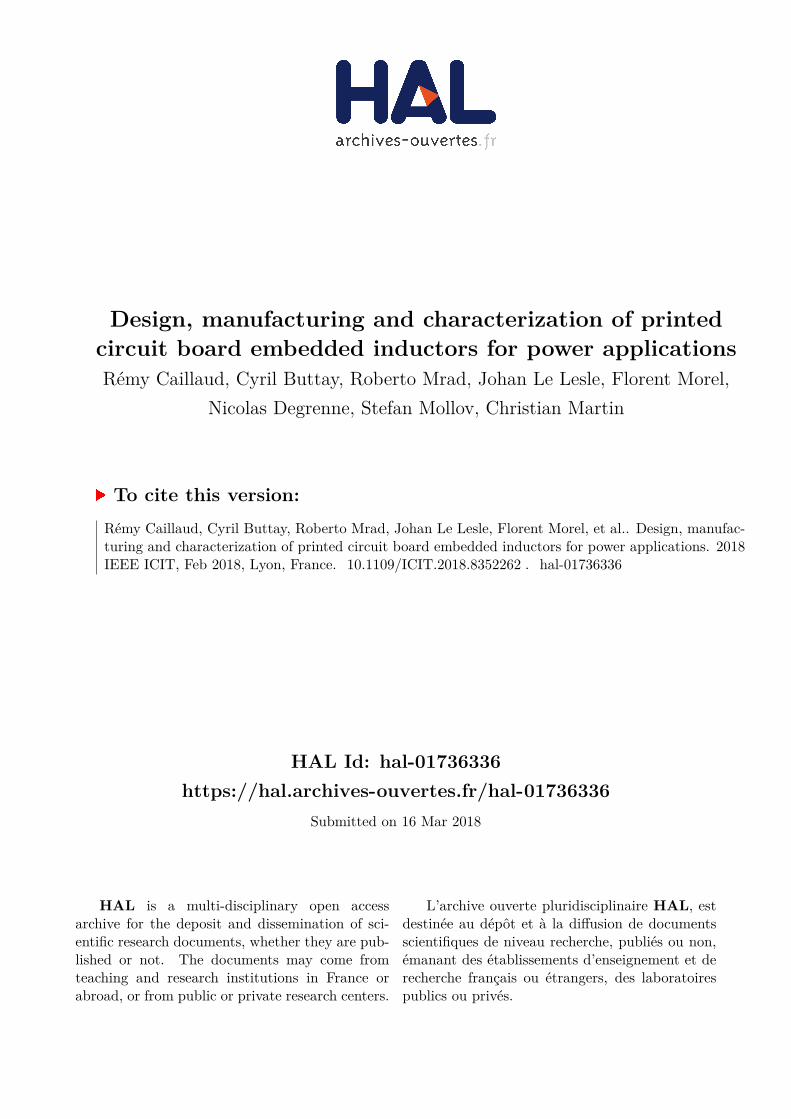
The inductor structure chosen for our converter is referredto as “toroidal embedded”. It uses PCB with a cavity to host atoroidal magnetic core. The winding is manufactured aroundthe magnetic core by patterning the PCB copper layers andplacing vias for the interconnections. The structure is presentedin Fig. 1.
An automated design procedure was set-up to compare thetoroidal embedded structure with more classical structuressuch as planar or wire-wound cores [10]. This design proce-dure allows to investigate many parameters such as magnetic
materials or core geometries, and automatically checks thatthe configuration meets the PCB design rules. For a chosenstructure, material and core size, a program calculates thenumber of turns required to achieve the desired inductancevalue. Then, this configuration is checked for saturation ofthe magnetic core. For ferrite materials, an air-gap is designedto prevent saturation, while for iron powder materials (whichhave a distributed air gap) the configuration which lead tosaturation are simply discarded.
For all acceptable configurations, the inductor losses arecalculated using the improved Generalized Steinmetz Equation(iGSE) for core losses and FEM simulation for copper losses(to account for skin and proximity effects). A 2D thermal FEMsimulation is then run to ensure the inductor remains belowa fixed temperature limit (100 C). All configurations whichresult in higher temperature are discarded. The best inductoris defined by the best trade-off between losses and boxvolume [10]. Finally, the program generates an script, whichis run in the PCB design software (Altium) to automaticallyproduce the Gerber files for the selected inductor.
It was found that the toroidal embedded structure presentsthe best trade-off between losses and box volume due to itsbetter cooling capability (its flat shape results in large surfacesfor heat exchange). This structure was chosen to be used forthe EMI differential mode (DM) filter inductor in a PowerFactor Corrector (PFC) application. The corresponding designparameters are listed in table I.
Table I: Prototypes parameters. Two inductors designs are considered: a “test”inductor, used for technology set-up, and a “filter” inductor, for the applicationdescribed in section II.
Properties Test inductor EMI Filter inductorCore thickness 3 mm 3 mmCopper thickness 105 µm 105 µmVia hole drilling diameter 0.6 mm 0.6 mmMagnetic material MPP200 Ferrite N87Outer Diameter 27.7 mm 50 mmInner Diameter 14.1 mm 30 mmNumber of turns 18 16Air-gap – 1.3 mmµr / µeff 200 96Expected Inductance 18.1 µH 7.95 µHRDC 156 mΩ 35 mΩIMax 5 A 21.2 A
Fig. 1: 3D view of the toroidal embedded structure. The PCB material is notrepresented.
(a)
(b)
(c)
(d)
(e)
(f)
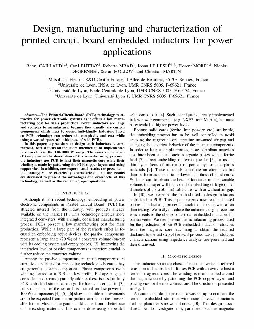
Fig. 2: Process flow for the fabrication of a PCB embedded inductor.
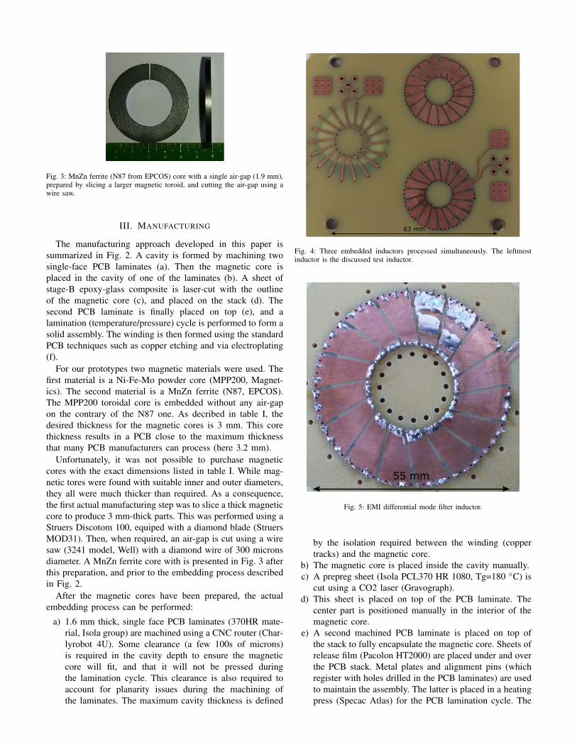
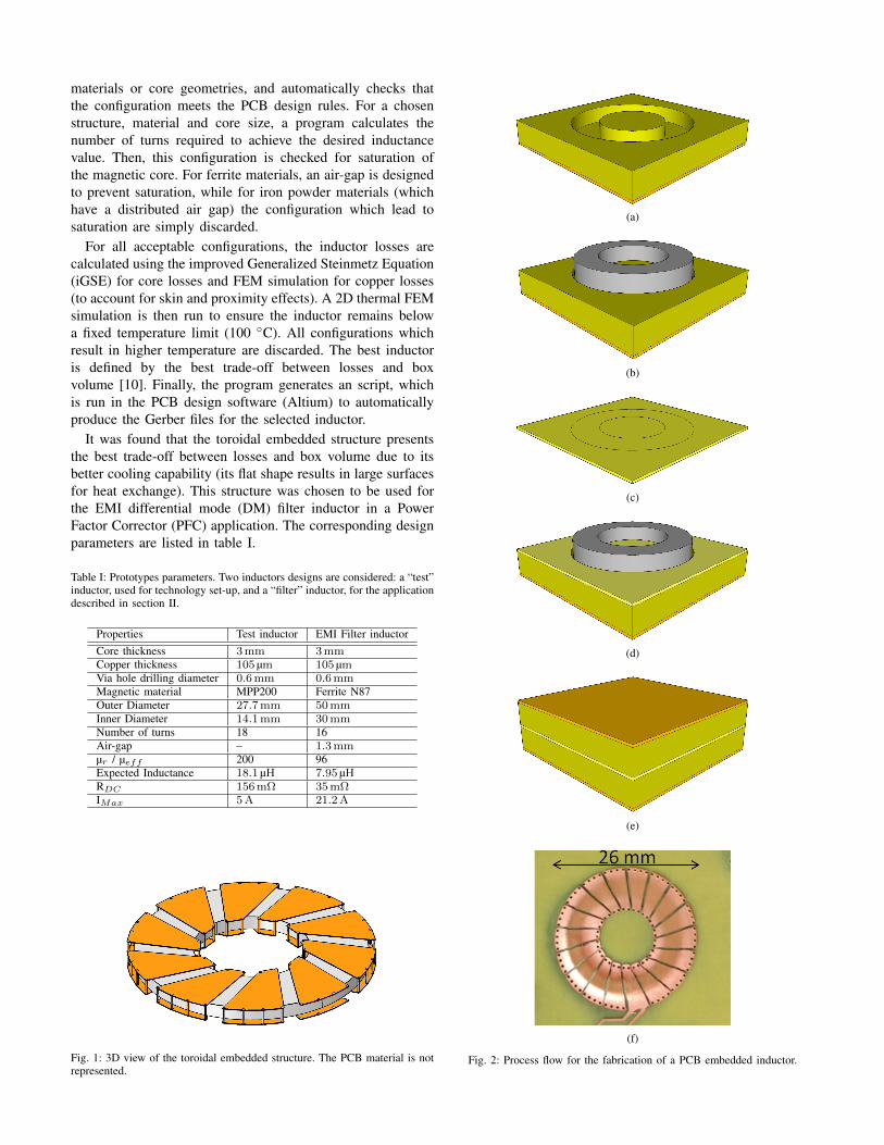
Fig. 3: MnZn ferrite (N87 from EPCOS) core with a single air-gap (1.9 mm),prepared by slicing a larger magnetic toroid, and cutting the air-gap using awire saw.
III. MANUFACTURING
The manufacturing approach developed in this paper issummarized in Fig. 2. A cavity is formed by machining twosingle-face PCB laminates (a). Then the magnetic core isplaced in the cavity of one of the laminates (b). A sheet ofstage-B epoxy-glass composite is laser-cut with the outlineof the magnetic core (c), and placed on the stack (d). Thesecond PCB laminate is finally placed on top (e), and alamination (temperature/pressure) cycle is performed to form asolid assembly. The winding is then formed using the standardPCB techniques such as copper etching and via electroplating(f).
For our prototypes two magnetic materials were used. Thefirst material is a Ni-Fe-Mo powder core (MPP200, Magnet-ics). The second material is a MnZn ferrite (N87, EPCOS).The MPP200 toroidal core is embedded without any air-gapon the contrary of the N87 one. As decribed in table I, thedesired thickness for the magnetic cores is 3 mm. This corethickness results in a PCB close to the maximum thicknessthat many PCB manufacturers can process (here 3.2 mm).
Unfortunately, it was not possible to purchase magneticcores with the exact dimensions listed in table I. While mag-netic tores were found with suitable inner and outer diameters,they all were much thicker than required. As a consequence,the first actual manufacturing step was to slice a thick magneticcore to produce 3 mm-thick parts. This was performed using aStruers Discotom 100, equiped with a diamond blade (StruersMOD31). Then, when required, an air-gap is cut using a wiresaw (3241 model, Well) with a diamond wire of 300 micronsdiameter. A MnZn ferrite core with is presented in Fig. 3 afterthis preparation, and prior to the embedding process describedin Fig. 2.
After the magnetic cores have been prepared, the actualembedding process can be performed:
a) 1.6 mm thick, single face PCB laminates (370HR mate-rial, Isola group) are machined using a CNC router (Char-lyrobot 4U). Some clearance (a few 100s of microns)is required in the cavity depth to ensure the magneticcore will fit, and that it will not be pressed duringthe lamination cycle. This clearance is also required toaccount for planarity issues during the machining ofthe laminates. The maximum cavity thickness is defined
63 mm
Fig. 4: Three embedded inductors processed simultaneously. The leftmostinductor is the discussed test inductor.
55 mm
Fig. 5: EMI differential mode filter inductor.
by the isolation required between the winding (coppertracks) and the magnetic core.
b) The magnetic core is placed inside the cavity manually.c) A prepreg sheet (Isola PCL370 HR 1080, Tg=180 C) is
cut using a CO2 laser (Gravograph).d) This sheet is placed on top of the PCB laminate. The
center part is positioned manually in the interior of themagnetic core.
e) A second machined PCB laminate is placed on top ofthe stack to fully encapsulate the magnetic core. Sheets ofrelease film (Pacolon HT2000) are placed under and overthe PCB stack. Metal plates and alignment pins (whichregister with holes drilled in the PCB laminates) are usedto maintain the assembly. The latter is placed in a heatingpress (Specac Atlas) for the PCB lamination cycle. The

Frequency (Hz)102 104 106 108
Nor
mal
ized
Indu
ctan
ce
-0.2
0
0.2
0.4
0.6
0.8
1
1.2
1.4Core (Wire Winding)Embedded Core (Wire Winding) No Copper on PCBEmbedded Core (PCB Winding)
Fig. 6: Electrical characterization of the test inductor in the following con-figurations: before embedding process (with wire winding), after embeddingprocess in a blank PCB (with wire winding, no copper on the PCB), and afterthe full embedding process (with PCB winding).
temperature is increased at a rate of 6 C/min, up to195 C and it is maintained at this level for 90 minutes.The laminating pressure is 10 bar at the beginning and isthen increased up to 20 bar once the temperature exceeds100 C. At the end of this cycle, the assembly forms aunique, solid part.
f) Via holes (used to form the winding) are drilled in thePCB laminate using a CNC drill (Bungard CCD/2/ATC).The holes are plated with copper, using regular PCBchemistry (Bungard, using a Compacta plating stationfrom the same manufacturer). Finally, the copper layersare selectively masked with a photosensitive dry film(Dupont Riston), according to the Gerber files generatedby the design program, and patterned using ferric chlo-ride.
Photographs of the various inductors produced using thisprocess are given in Fig. 2(f), 4 and 5.
IV. CHARACTERIZATION
The data presented here was acquired using an impedanceanalyzer (Keysight E4294A) with a 42941A probe. A SMAconnector is soldered on the PCB for easy and reliableconnection with the probe.
The electrical characterization of the test inductor is pre-sented in Fig. 6. Three configurations were investigated: asimple magnetic core with wire winding (to make sure thecore properties were not affected by the slicing process); themagnetic core embedded in a blank PCB (no copper), alsousing wire winding (to measure the effect of embedding); andthe magnetic core embedded in a PCB with printed winding(the final version). As a different number of turns was usedin the three cases, Fig. 6 presents the normalized inductancevalue as a function of the frequency. For the embedded testinductor using PCB winding, the low frequency inductancevalue is 17.6 µH corresponding to the expected inductance18.1 µH.
A micro-section of the test inductor, realized with a scan-ning electron microscope (Vega 3, Tescan), is presented inFig. 7. This micro-section shows the magnetic core inside thecavity, with ≈ 400 µm clearance between the core and the topof the cavity. No damage is noticeable on the core, except
Magnetic core
Cavity
Glass-epoxy compositeResin flow
Copper layer
Fig. 7: Micro-section of the test inductor. Core is maintained inside thecavity at the middle by the prepreg sheet resine. The vias winding are notshown. The barrel shape is an artefact caused by using the microscope at lowmagnification. The outer surfaces of the sample are actually flat.
Frequency (Hz)102 103 104 105 106 107
Impe
danc
e (Ω
)
1
10
100
1 0002 000
Res
ista
nce
(Ω)
1
10
100
1 0002 000
(a)
Frequency (Hz)102 103 104 105 106 107
Pha
se (
°)
0
20
40
60
80
100
Indu
ctan
ce (µ
H)
10
12
14
16
18
20
(b)
Fig. 8: Electrical characterization of Differential Mode inductor using N87ferrite with a single air-gap (a) Impedance and resistance (b) Phase andinductance.
some chipping on the edges (which might have been causedduring the preparation of the micro-section). Some of the resinflowed in the cavity during the lamination and maintains themagnetic core. The rest of the cavity remains empty.
The electrical characterization of the EMI DM Filter induc-tor is presented in Fig. 8 for the magnetic core embedded witha PCB winding (PCB copper tracks and vias). The impedanceand resistance are traced as a function of the frequency inFig. 8a. The phase and inductance are plotted as function of thefrequency in Fig. 8b. The impedance and resistance are traced
using a logarithmic scale to show their dramatic increase atrelatively low frequency (tens of kHz). For this inductor, theinductance value at low frequency is 16.7 µH.
V. DISCUSSION
As seen in the micro-section in Fig. 7, the embeddingprocess is well controlled, and offers sufficient clearance toavoid stress on the brittle magnetic core during the laminationprocess. Even with the reduction in thickness of the prepreglayers (due to resin creep), the cavity remains taller than themagnetic core. The small amount of resin which flows out ofthe prepreg layers is not sufficient to fill the cavity, but offerssatisfying bonding to prevent the magnetic core from moving.Therefore, it is not expected that the magnetic core behaviouris affected by the embedding process.
The inductance shows a good behavior (constant inductancevalue) for all samples in the low frequency range (up to a fewtens of kHz). For Ni-Fe-Mo powder core (test inductor), theinductance value in low frequency is 17.6 µH for a calculatedvalue of 18.1 µH . The little difference can be explained bya poor control of the magnetic core thickness (this was ourfirst prototype). Further magnetic cores were sliced with adedicated fixture, resulting in much better thickness control.For the MnZn core (EMI filter DM inductor), the inductancevalue in low frequency is 16.7 µH for a calculated by thedesign script and expected value of 7.95 µH. This is a muchlarger error which is due to the fringing effect around theair gap. In the design script, the section of the air-gap isconsidered identical to that of the magnetic core. But withan air-gap length of 1.3 mm for a core thickness of 3 mm,this assumption no longer holds true: the aspect ratio betweenthe air-gap length and the core thickness is not negligible,resulting in a much larger equivalent section of the air-gap.The design procedure has to be modified to take into accountthe influence of the fringing effect on the reluctance of theair-gap [11].
A second issue is the inductance behavior at higher fre-quency. Above a few tens of kHz, the inductance value de-creases and the serial resistance value increases strongly. Thisis not acceptable, as these inductors were designed to be usedin a converter with a switching frequency of 180 kHz. Thisbehavior is not due to the core machining or the embeddingprocess, since the non-embedded core or the embedded corewith classic wire winding does not show this behavior (Fig. 6).
A second possible cause is the capacitance between PCBwinding and the core, which is larger than with a wire-wound inductor. This capacitance is calculated using planecapacitor formula. The inter-winding capacitance is neglected,due to the low copper thickness compared to the copper tracklength and width. The capacitance calculated for the EMI filterDM inductor is 442 pH which results in a cut-off frequencyclose to 1.9 MHz, much higher than the frequency of theobserved inductance drop. In addition, the routing of the testinductor (Fig. 4) is similar to a classic wire winding, withthin copper stripes (instead of the larger tracks visible, forexample, in Fig. 4), which generate a much smaller parasiticcapacitance. And yet, the inductance also drops earlier for the
Air-Gap Position103 °C
38 °C
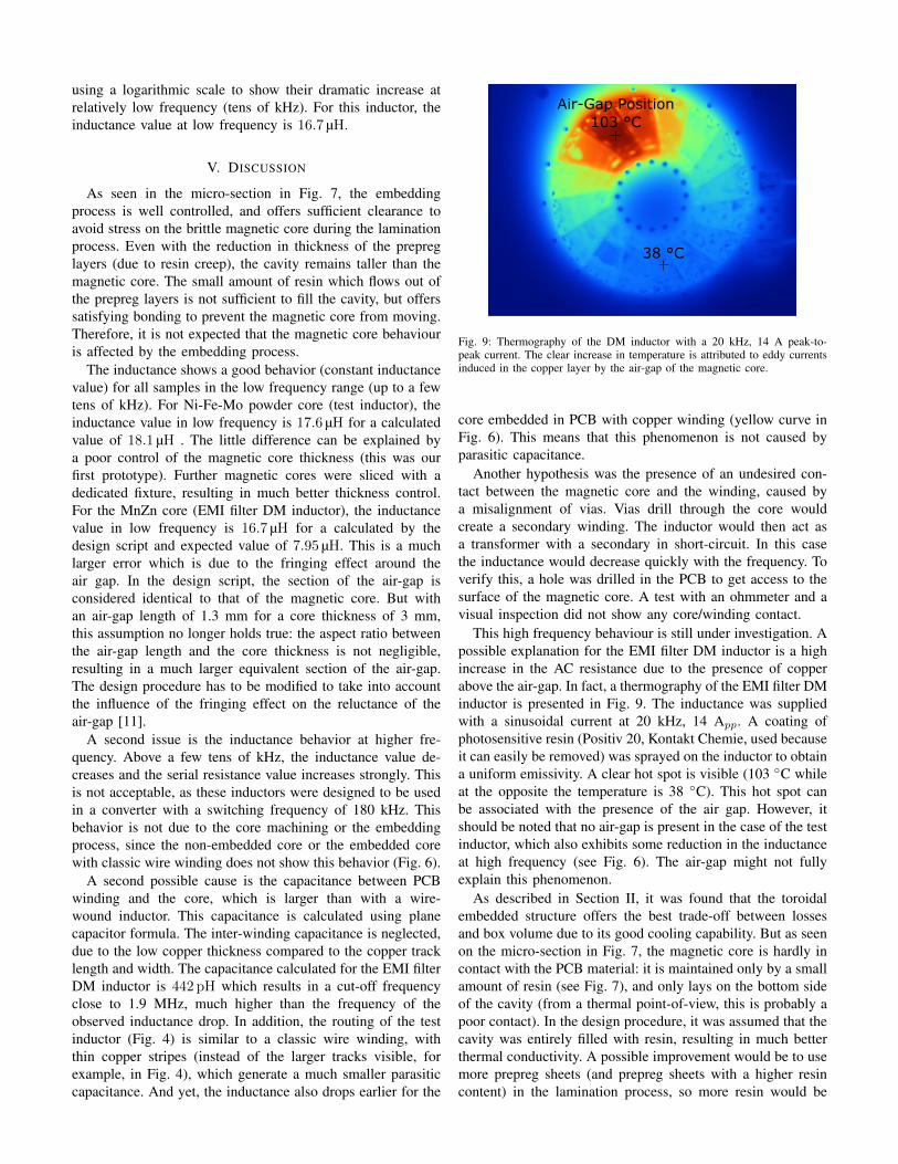
Fig. 9: Thermography of the DM inductor with a 20 kHz, 14 A peak-to-peak current. The clear increase in temperature is attributed to eddy currentsinduced in the copper layer by the air-gap of the magnetic core.
core embedded in PCB with copper winding (yellow curve inFig. 6). This means that this phenomenon is not caused byparasitic capacitance.
Another hypothesis was the presence of an undesired con-tact between the magnetic core and the winding, caused bya misalignment of vias. Vias drill through the core wouldcreate a secondary winding. The inductor would then act asa transformer with a secondary in short-circuit. In this casethe inductance would decrease quickly with the frequency. Toverify this, a hole was drilled in the PCB to get access to thesurface of the magnetic core. A test with an ohmmeter and avisual inspection did not show any core/winding contact.
This high frequency behaviour is still under investigation. Apossible explanation for the EMI filter DM inductor is a highincrease in the AC resistance due to the presence of copperabove the air-gap. In fact, a thermography of the EMI filter DMinductor is presented in Fig. 9. The inductance was suppliedwith a sinusoidal current at 20 kHz, 14 App. A coating ofphotosensitive resin (Positiv 20, Kontakt Chemie, used becauseit can easily be removed) was sprayed on the inductor to obtaina uniform emissivity. A clear hot spot is visible (103 C whileat the opposite the temperature is 38 C). This hot spot canbe associated with the presence of the air gap. However, itshould be noted that no air-gap is present in the case of the testinductor, which also exhibits some reduction in the inductanceat high frequency (see Fig. 6). The air-gap might not fullyexplain this phenomenon.
As described in Section II, it was found that the toroidalembedded structure offers the best trade-off between lossesand box volume due to its good cooling capability. But as seenon the micro-section in Fig. 7, the magnetic core is hardly incontact with the PCB material: it is maintained only by a smallamount of resin (see Fig. 7), and only lays on the bottom sideof the cavity (from a thermal point-of-view, this is probably apoor contact). In the design procedure, it was assumed that thecavity was entirely filled with resin, resulting in much betterthermal conductivity. A possible improvement would be to usemore prepreg sheets (and prepreg sheets with a higher resincontent) in the lamination process, so more resin would be

available to flow and fill the cavity. However, more prepreglayers would contract more during the lamination; special caremust then be given to prevent the cavity to shrink too much, asthis would result in a contact between the magnetic core andthe PCB laminates, and a non-uniform pressure distribution.
VI. CONCLUSION
The toroidal embedded structure is attractive for large powermagnetic components (inductors). Its manufacturing processrelies on standard PCB technology, and allows to manufactureseveral inductors in a single process. The custom inductorgeometry is automatically generated by the design program.
The lab-scale manufacturing process was detailed and usedto produce several prototypes. A cavity is machined in PCBlaminates to receive a magnetic core. As the cavity is slightlytaller than the magnetic core, no pressure is transferred tothe core during lamination. This prevents cracking this brittlematerial. However, this causes large parts of the cavity toremain empty, resulting in poor thermal exchange between thecore and its environment. This might prove to be an issue andmight require improvements of the manufacturing processes.
Demonstrators were made using Ni-Fe-Mo powder core andMnZn ferrite core. They show a good inductance behavior inthe low frequency. But the inductance value decreases abovea few tens of kHz. This phenomena can be explained onthe MnZn ferrite sample by the eddy currents induced in thecopper layers by the magnetic field fringing from the largeair-gap. However, for the Ni-Fe-Mo powder inductors, whichhave a distributed air gap, no explanation can currently beoffered and this is still under investigation.
The design and manufacturing processes will now be op-timized to take into account the fringing effect and the resinflow to improve thermal management. Future characterizationwill be performed in a calorimeter to accurately measure thelosses in the inductor.
REFERENCES
[1] A. Ostmann, L. Boettcher, D. Manessis, S. Karaszkiewicz, and K.-D.Lang, “Power modules with embedded components,” in MicroelectronicsPackaging Conference (EMPC) , 2013 European, Sep. 2013, pp. 1–4.
[2] J. Popovic-Gerber, “Passive Components Packaging,” in ECPE Tutorial"Power Electronics Packaging", 2015, pp. 1–79.
[3] M. Ali, E. Labouré, F. Costa, and B. Revol, “Design of a Hybrid Inte-grated EMC Filter for a DC-DC Power Converter,” IEEE Transactionson Power Electronics, vol. 27, no. 11, pp. 4380–4390, 2012.
[4] Q. Chen, Z. Gong, X. Yang, Z. Wang, and L. Zhang, “Design con-siderations for passive substrate with ferrite materials embedded inprinted circuit board (pcb),” in 2007 IEEE Power Electronics SpecialistsConference, June 2007, pp. 1043–1047.
[5] Y. Kondo, Y. Yazaki, M. Sonehara, T. Sato, T. Watanabe, Y. Seino,N. Matsushita, T. Fujii, K. Kobayashi, H. Shimizu et al., “Embeddedplanar power inductor technology for package-level DC power grid,” inElectronics Packaging and iMAPS All Asia Conference (ICEP-IACC),2015 International Conference on. IEEE, 2015, pp. 814–817.
[6] A. Alderman, L. Burgyan, B. Narveson, and E. Parker, “3-D EmbeddedPackaging Technology.” IEEE Power Electronics Magazine, pp. 30–39,2015.
[7] D. Bang and J. Park, “Ni-Zn ferrite screen printed power inductorsfor compact dc-dc power converter applications.” IEEE Transactionson Magnetics, vol. 45, no. 6, pp. 2762–2765, 2009.
[8] R. Caillaud, C. Buttay, J. Le Lesle, F. Morel, R. Mrad,N. Degrenne, S. Mollov, and C. Combettes, “High power PCB-embedded inductors based on ferrite powder.” [Online]. Available:https://hal.archives-ouvertes.fr/hal-01535727
[9] C. Marxgut, J. Muhlethaler, F. Krismer, and J. W. Kolar, “Multiobjectiveoptimization of ultraflat magnetic components with pcb-integrated core,”IEEE Transactions on Power Electronics, vol. 28, no. 7, pp. 3591–3602,2013.
[10] R. Caillaud, C. Buttay, R. Mrad, J. Le Lesle, F. Morel, N. Degrenne, andS. Mollov, “Comparison of planar and Toroidal PCB integrated inductorsfor a multi-cellular 3.3 kW PFC.” in IEEE International Workshop OnIntegrated Power Packaging (IWIPP), 2017.
[11] A. Balakrishnan, W. T. Joines, S. Member, T. G. Wilson, and L. Fellow,“Air-Gap Reluctance and Inductance Calculations for Magnetic CircuitsUsing a Schwarz - Christoffel Transformation,” IEEE Transactions onPower Electronic, vol. 12, no. 4, pp. 654–663, 1997.